Frameless OLED Pushbutton · 2020-01-09 · Frameless OLED Pushbutton E4 E Indicators Accessories...
6
Frameless OLED Pushbutton www.nkkswitches.com E4 E Indicators Accessories Supplement Tactiles Keylocks Rotaries Pushbuttons Illuminated PB Slides Programmable Rockers Touch Tilt Toggles DISTINCTIVE CHARACTERISTICS • High definition, contrast and resolution of 96RGB x 64 pixels in compact screen and minimal frame • Range of 65,536 colors in 16 bit mode • Operating life of 50,000 hours minimum • Maximum use of display lens with ultra-thin frame provides full screen capacity • Multiple units easily combine to form one screen, offering flexibility in size and layout • Smooth operation with short stroke of 0.07” lends to tactile feedback unparalleled to touch panels • Same outer dimensions of switch and footprint, enabling ease of replacement with current switches • Operated by commands and data supplied via serial communications (SPI) • Incorporates bitmap display function • Low energy consumption • Dust tight construction • Snap-in standoff for easy, secure mounting and alignment; aids in prevention of dislodging during wave soldering Actual Size Viewing area: 21.28mm x 18.7mm (horizontal x vertical) High reliability and long life of one million actuations minimum Highly reliable gold plated twin contacts Epoxy sealed straight PC terminals 10/03/19
Transcript of Frameless OLED Pushbutton · 2020-01-09 · Frameless OLED Pushbutton E4 E Indicators Accessories...
Frameless OLED Pushbutton
www.nkkswitches.comE4
E
Indi
cato
rsA
cces
sori
esSu
pple
men
tTa
ctile
sK
eylo
cks
Rota
ries
Push
butto
nsIll
umin
ated
PB
Slid
esPr
ogra
mm
able
Rock
ers
Touc
hTi
lt To
ggle
s
DISTINCTIVE CHARACTERISTICS
• High definition, contrast and resolution of 96RGB x 64 pixels in compact screen and minimal frame
• Range of 65,536 colors in 16 bit mode
• Operating life of 50,000 hours minimum
• Maximum use of display lens with ultra-thin frame provides full screen capacity
• Multiple units easily combine to form one screen, offering flexibility in size and layout
• Smooth operation with short stroke of 0.07” lends to tactile feedback unparalleled to touch panels
• Same outer dimensions of switch and footprint, enabling ease of replacement with current switches
• Operated by commands and data supplied via serial communications (SPI)
• Incorporates bitmap display function
• Low energy consumption
• Dust tight construction
• Snap-in standoff for easy, secure mounting and alignment;aids in prevention of dislodging during wave soldering
Actual Size
Viewing area: 21.28mm x 18.7mm (horizontal x vertical)
High reliability and long life of one million actuations minimum
Highly reliable gold plated twin contacts
Epoxy sealed straight PC terminals
10/03/19
Frameless OLED Pushbutton
www.nkkswitches.com E5
E
Indi
cato
rsA
cces
sori
esSu
pple
men
tTa
ctile
sK
eylo
cks
Rota
ries
Push
butto
nsIll
umin
ated
PB
Slid
esPr
ogra
mm
able
Togg
les
Rock
ers
Touc
hTi
lt
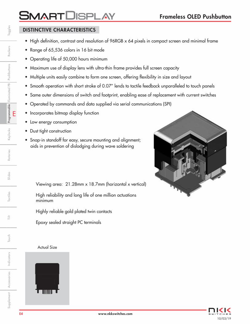
SWITCH SPECIFICATIONS
OLED SPECIFICATIONS
Absolute Maximum Ratings
Items Symbols Ratings
Supply Voltage for Logic/Interface VDD –0.3V to +4.0V
Supply Voltage for Drive VCC –0.0V to +19.0V
Input Voltage VI –0.3V to VDD +0.3V
Recommended Operating Conditions
Items Symbols Minimum Typical Maximum
Supply Voltage for Logic/Interface VDD 2.4V 2.8V 3.5V
Supply Voltage for Drive VCC 14.0V 15.0V 16.0V
Input High Level Voltage VIH 0.8 x VDD –– ––
Input Low Level Voltage VIL –– –– 0.2 x VDD
Characteristics of DisplayDisplay Device Color OLED display module
Display Mode Passive matrix
Viewing Area 21.28mm x 18.74mm (horizontal x vertical)
Pixel Format 96RGB x 64 pixels (horizontal x vertical)
Pixel Size 0.222mm x 0.293mm (horizontal x vertical)
Interface Serial (SPI) interface
Number of Colors 65,536 Colors (16bit: R 5bit/G 6bit/B 5bit) or 256 Colors (8bit: R 2bit/G 3bit/B 3bit)
Operating Temperature Range –20°C ~ +70°C (–4°F ~ +158°F)
Storage Temperature Range –30°C ~ +80°C (–22°F ~ +176°F)
Operating Life (Display) 50,000 hours @ 100cd/m2 (based on 40% pixels ON; Ta = 77°F)
Current Consumption (Temperature at 25°C, VDD = 2.8V, VCC = 15.0V)
Items Symbols Min Typical Max
All-Pixels-On Mode *Drive System Power Current I CC1 –– 11.0mA 13.2mA
All-Pixels-On Mode *Logic/IF System Power Current I DD1 –– 0.17mA 0.20mA
Sleep Mode **Drive System Power Current I CC2 –– –– 10μA
Sleep Mode **Logic/IF System Power Current I DD2 –– –– 10μA
* All pixels shall be turned on with the maximum level gray scale** All pixels shall be turned off (while chip is operating)
Circuit SPST normally open
Contact Position Leave actuator: 1 – 2 OFF Push actuator: 1 – 2 ON
Electrical Capacity (Resistive Load) 100mA @ 12V DC (resistive circuit)
Contact Resistance 200 milliohms maximum @ 20mV 10mA
Insulation Resistance 100 megohms minimum @ 100V DC
Dielectric Strength 125V AC for 1 minute minimum
Mechanical Endurance 1,000,000 operations minimum
Electrical Endurance 1,000,000 operations minimum
Operating Force 2.0 ± 0.5 Newtons
Total Travel 1.8mm (0.07”)
Optical Characteristics (Temperature at 25°C, Initial Value: 87 x 0F)
Items Min Typical Max Unit Remarks
Luminosity 80 105 130 cd/m2 White (All pixels on)
White Color Coordinate
(x) 0.26 0.30 0.34 ––(y) 0.31 0.36 0.41 ––
Red Color Coordinate
(x) 0.62 0.66 0.70 ––(y) 0.30 0.34 0.38 ––
Green Color Coordinate
(x) 0.24 0.29 0.33 ––(y) 0.59 0.63 0.67 ––
Blue Color Coordinate
(x) 0.10 0.15 0.19 ––(y) 0.10 0.17 0.23 ––
Contrast Ratio 100 –– –– ––
Part Number Switch Description OLED Pixel Format
ISF15ACP4SPST, Momentary ON
Gold ContactsStraight PC Terminals
Color OLEDDisplay Module65,536 Colors
96RGB x 64 PixelsHorizontal x Vertical
SWITCH PART NUMBER & DESCRIPTIONATTENTION
ELECTROSTATICSENSITIVE DEVICES

Frameless OLED Pushbutton
www.nkkswitches.comE6
E
Indi
cato
rsA
cces
sori
esSu
pple
men
tTa
ctile
sK
eylo
cks
Rota
ries
Push
butto
nsIll
umin
ated
PB
Slid
esPr
ogra
mm
able
Rock
ers
Touc
hTi
lt To
ggle
s
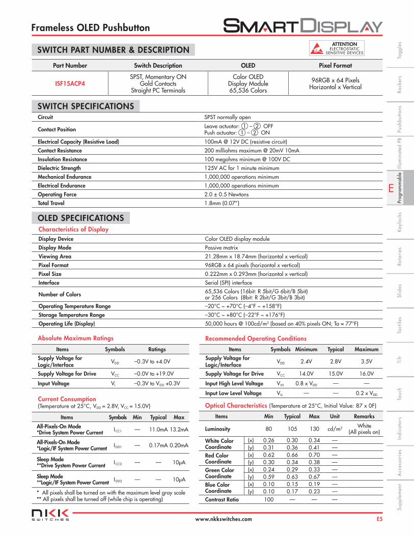
Terminal numbers are not on the switch.
BLOCK DIAGRAM & PIN CONFIGURATIONS
TYPICAL SWITCH DIMENSIONS
Pixel Detail Standoff Detail
Dimension AStandoff 1 = (2.7)
.106Standoff 2 = (2.3)
.091
Footprint
Driving BlockSEG/COM
Segment Driver
SR1, SG1, SB1......SR96,SG96,SB96
Color OLED Panel96RGB x 64
SW
Gray Scale
Common Driver
COM1....COM64
Display Timing
Oscillator
Generator
Decoder
Command Decoder
Graphic DisplayData RAM96 x 64 x 16 Bit
MCU Interface
OLED Driverwith Controller
SW 1
CCV 9
DDV 3
RES 5
SCK 7
4SS
8SDI
6D/C
GND 10
2
ISF15ACP4
(23.13).911
(21.28).838
(20.59).811
(18.74).738
Part No.This Side
(23.13).911
(18.0).709
(16.0).630
(7.62).300
(8.0).315
(7.05).278
(2.0).079
(1.0) Typ.039
(7.0).276
89
45
67
3
2
1
10
Standoff 1 Standoff 2
Standoff 2 Standoff 1
(0.3) Typ.012
(0.2).008
A
(1.25).049
(2.0) Dia.079
910
34
2
1
(18.0).709
(1.0) Typ.039
(7.0).276
(2.0).079
(7.05).278
(8.0).315
4x (1.3) Dia .051Landless
(7.62).300
(16.0).630
2x (0.9) Dia .035
8x (0.75) Dia .030
R G B R
R
(.263).0104
(.293).0115
(.044).0017
(.074).0029
(.222).0087
Pin No. Symbol Name Function
SW Terminal of Switch Normally openSW Terminal of Switch Normally openVDD Power Power source for logic circuitSS Slave Select Slave select for SPI. This line is active low.
RES Reset Reset signal input. When pin is low, initialization of chip is executed.
D/C Data/CommandData/Command Control. When pin is pulled low, data will be interpreted as Command; when pulled high, data will be interpreted as Data.
SCK Serial Clock Clock line for SPI that synchronizes command and dataSDI Serial Data In Data input line for SPIVCC Power Power source for drive circuit
GND Ground Connect to Ground
6
5
4321
987
10
(23.0).906
(3.4).134
(0.4).016
(3.3).130
(0.6).024
See StandoffDetail
Frameless OLED Pushbutton
www.nkkswitches.com E7
E
Indi
cato
rsA
cces
sori
esSu
pple
men
tTa
ctile
sK
eylo
cks
Rota
ries
Push
butto
nsIll
umin
ated
PB
Slid
esPr
ogra
mm
able
Togg
les
Rock
ers
Touc
hTi
lt
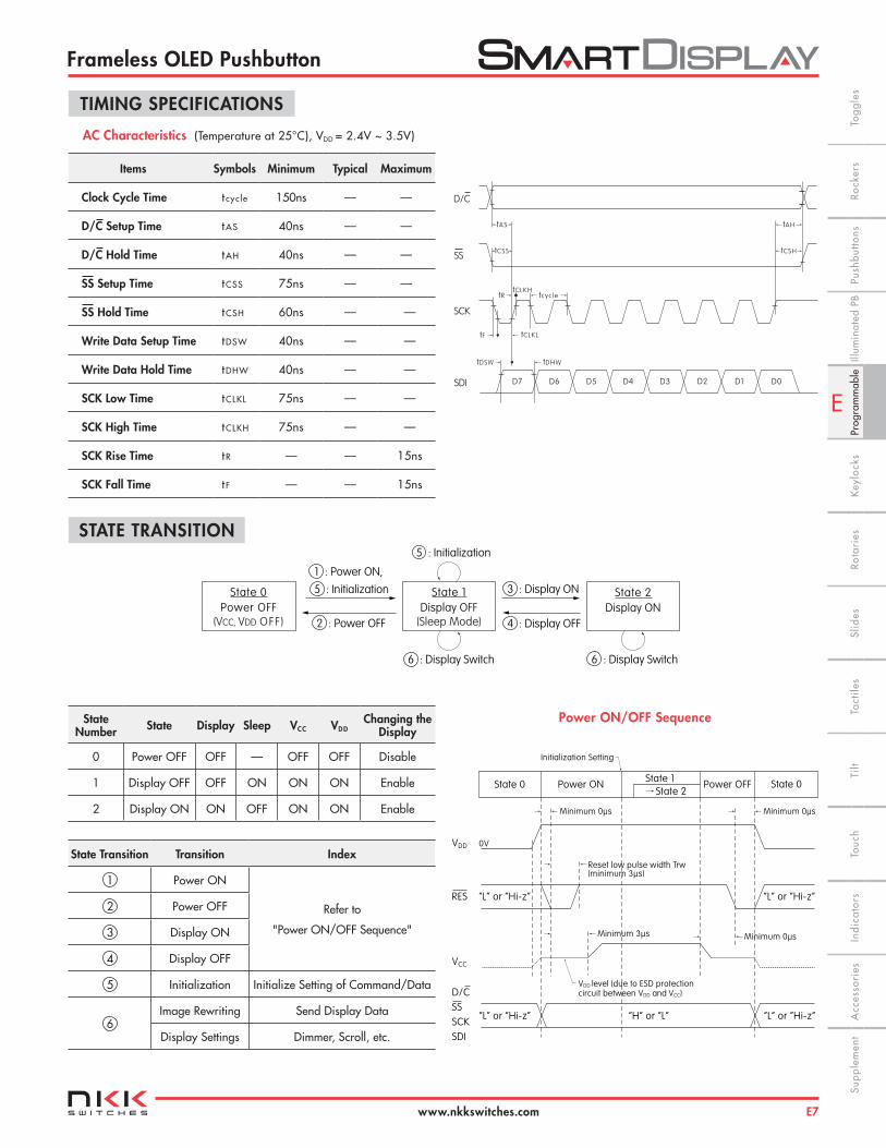
TIMING SPECIFICATIONS
State Transition Transition Index
1 Power ON
Refer to
"Power ON/OFF Sequence"
2 Power OFF
3 Display ON
4 Display OFF
5 Initialization Initialize Setting of Command/Data
6Image Rewriting Send Display Data
Display Settings Dimmer, Scroll, etc.
State Number State Display Sleep VCC VDD
Changing theDisplay
0 Power OFF OFF –– OFF OFF Disable
1 Display OFF OFF ON ON ON Enable
2 Display ON ON OFF ON ON Enable
STATE TRANSITION
D/C
SS
SDI
tAS
D7 D6 D5 D4 D3 D2 D1 D0
tCSS tCSH
tAH
tCLKHtcyc le
tCLKLtF
SCK
tDHWtDSW
tR
State 0Power OFF
(VCC, VDD OFF )
State 1Display OFF
(Sleep Mode)
State 2Display ON
1 : Power ON,
5 : Initialization
2 : Power OFF
3 : Display ON
4 : Display OFF
6 : Display Switch6 : Display Switch
5 : Initialization
State 0 Power ONState 1
State 2Power OFF State 0
VDD
RES
VCC
D/CSSSCKSDI
Reset low pulse width Trw(minimum 3µs)
“L” or “Hi-z”
0V
Minimum 0µs Minimum 0µs
“L” or “Hi-z”
Minimum 3µs Minimum 0µs
VDD level (due to ESD protection circuit between VDD and VCC)
“L” or “Hi-z”“H” or “L”“L” or “Hi-z”
Initialization Setting
Power ON/OFF Sequence
AC Characteristics (Temperature at 25°C), VDD = 2.4V ~ 3.5V)
Items Symbols Minimum Typical Maximum
Clock Cycle Time t cyc le 150ns –– ––
D/C Setup Time tAS 40ns –– ––
D/C Hold Time tAH 40ns –– ––
SS Setup Time tCSS 75ns –– ––
SS Hold Time tCSH 60ns –– ––
Write Data Setup Time tDSW 40ns –– ––
Write Data Hold Time tDHW 40ns –– ––
SCK Low Time tCLKL 75ns –– ––
SCK High Time tCLKH 75ns –– ––
SCK Rise Time t R –– –– 15ns
SCK Fall Time t F –– –– 15ns
OLED Pushbutton & Display
www.nkkswitches.comE14
E
Indi
cato
rsA
cces
sori
esSu
pple
men
tTa
ctile
sK
eylo
cks
Rota
ries
Push
butto
nsIll
umin
ated
PB
Slid
esPr
ogra
mm
able
Rock
ers
Touc
hTi
lt To
ggle
s
PRECAUTIONS FOR HANDLING & STORAGE OF OLED PUSHBUTTONS & DISPLAY
Handling
1. The IS Series OLED devices are electrostatic sensitive. To avoid damage to IC,do not touch terminals unless properly isolated from static electricity.
2. Signal input under conditions not recommended may cause damage to the OLED unit or deterioration of thedisplay. Follow directions regarding supply sequences of power and signal voltages.
3. If the OLED panel is broken, avoid touching the contents. Wash off any contact to the skin or clothing.
4. Limit operating force to switch keytop to 100.0N maximum, as excessive pressure may damage the OLED.
5. For OLED display, it is necessary for bracket legs to be Grounded.
6. Recommended soldering time and temperature limits for OLED switch or display:
Avoid temperatures exceeding 80°C at the OLED.Wave Soldering: see Profile A in Supplement section.Manual Soldering: see Profile A in Supplement section.
7. The IS series OLED devices are not process sealed.
8. Pixels acquire diminished brightness over time and use, and those most frequently habituated have greaterreduction of brightness than those less used. To minimize this difference, operate OLED unit so that all pixelsare used as consistently as possible.
9. For switch, clean cap surface with dry cloth. If further cleaning is needed, wipe with dampened cloth usingneutral cleanser and dry with clean cloth. Do not use organic solvent. For display, avoid contact with anyflux or detergent. If any liquids spill on display surface, immediately wipe with soft absorbent cloth.
10. Proper serial resistors and buffers for signals should be used to prevent noise problems.
Storage
1. Store in original container and away from direct sunlight.
2. Keep away from static electricity.
3. Avoid extreme temperatures, high humidity, gaseous substances, and all forms of chemical contamination.
ATTENTIONELECTROSTATIC
SENSITIVE DEVICES
Optional Accessories
www.nkkswitches.comE50
E
Indi
cato
rsA
cces
sori
esSu
pple
men
tTa
ctile
sK
eylo
cks
Rota
ries
Push
butto
nsIll
umin
ated
PB
Slid
esPr
ogra
mm
able
Rock
ers
Touc
hTi
lt To
ggle
s
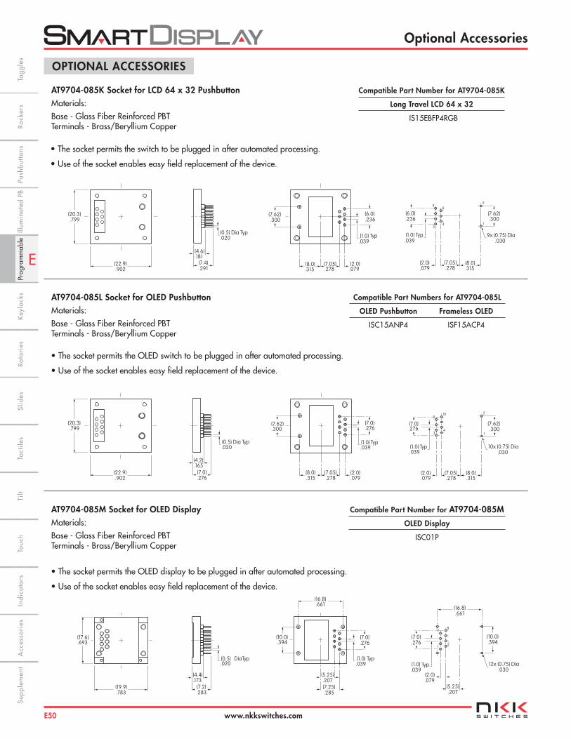
OPTIONAL ACCESSORIES
AT9704-085K Socket for LCD 64 x 32 PushbuttonMaterials: Base - Glass Fiber Reinforced PBTTerminals - Brass/Beryllium Copper
• The socket permits the switch to be plugged in after automated processing.
• Use of the socket enables easy field replacement of the device.
AT9704-085L Socket for OLED PushbuttonMaterials: Base - Glass Fiber Reinforced PBTTerminals - Brass/Beryllium Copper
AT9704-085M Socket for OLED DisplayMaterials: Base - Glass Fiber Reinforced PBTTerminals - Brass/Beryllium Copper
• The socket permits the OLED switch to be plugged in after automated processing.
• Use of the socket enables easy field replacement of the device.
• The socket permits the OLED display to be plugged in after automated processing.
• Use of the socket enables easy field replacement of the device.
(22.9).902
(20.3).799
(4.6).181
(0.5) Dia Typ.020
(7.4).291
(7.62).300
(8.0).315
(7.05).278
(2.0).079
(1.0) Typ.039
(6.0).236
(7.62).300
(8.0).315
(7.05).278
(2.0).079
(6.0).236
(1.0) Typ.039
9x (0.75) Dia .030
1
2
3
9
4
8
(22.9).902
(20.3).799
(7.62).300
(8.0).315
(7.05).278
(2.0).079
(7.0).276
(1.0) Typ.039
10x (0.75) Dia .030
1
2
3
9
4
10
(4.2).165
(7.0).276
(0.5) Dia Typ.020
(5.25).207
(2.0).079
(16.8).661
(10.0).394
(1.0) Typ.039
(7.0).276
12x (0.75) Dia .030
1
7
2
8
(4.4).173
(7.2).283
(0.5).020
DiaTyp
(19.9).783
(17.6).693
(16.8).661
(5.25).207(7.25).285
(10.0).394
(1.0) Typ.039
(7.0).276
(7.62).300
(8.0).315
(7.05).278
(2.0).079
(1.0) Typ.039
(7.0).276
Compatible Part Number for AT9704-085K
Long Travel LCD 64 x 32
IS15EBFP4RGB
Compatible Part Number for AT9704-085M
OLED Display
ISC01P
Compatible Part Numbers for AT9704-085L
OLED Pushbutton Frameless OLED
ISC15ANP4 ISF15ACP4