FR80 Family 32-BIT MICROCONTROLLER MB91F662€¦ · Requires two or more USB ports. 2 Software -...
143
FR80 Family 32-BIT MICROCONTROLLER MB91F662 bits pot black USB board User's Manual
Transcript of FR80 Family 32-BIT MICROCONTROLLER MB91F662€¦ · Requires two or more USB ports. 2 Software -...
FR80 Family 32-BIT MICROCONTROLLER
MB91F662
bits pot black
USB board
User's Manual

1
Disclaimer and Legal Notice
The contents of this document are subject to change without a prior notice, thus ask our
sales division about the latest one.
The descriptions of functions and application circuit examples in this document are provided
solely for the purpose of showing examples of standard operations and uses of the
semiconductor device, and FUJITSU MICROELECTRONICS does not warrant proper
operation of the device on any equipment in practical use. Therefore, if you make a design
based on the information in this document, you must assume responsibility for it; FUJITSU
MICROELECTRONICS assumes no liability for any damage or loss from use of the
information.
Any information in this document, including descriptions of functions and schematic circuit
diagrams, shall neither be construed as license of use or exercise of any intellectual
property right, patent right, copyright, and other right of FUJITSU MICROELECTRONICS or
any third party nor assured for use or exercise of any third-party's intellectual property right
or other right in use of the information. Therefore, FUJITSU MICROELECTRONICS
assumes no liability for any infringement of intellectual property right or other right of a third
party which would result from use of the information contained herein.
The products described in this document are designed, developed, and manufactured,
intended for general use such as ordinary industrial use, general office use, personal use,
and household use. That is, the products are not designed and manufactured intended for
use accompanying fatal risk or danger that, unless extremely high safety is secured, could
cause critical damage and could lead directly to death, personal injury, or severe physical
damage (i.e., nuclear reaction control in a nuclear facility, automatic aviation control,
aviation traffic control, mass transport system control, medical life support system control,
missile launch control in a weapon system), or for use requiring extremely high reliability
(i.e., submersible repeater and artificial satellite). Therefore, if you intend to use the
products for any of the purposes mentioned above, please be sure to have consultations
with our sales division about it. Otherwise, FUJITSU MICROELECTRONICS will not be
liable against any damage or loss from it.
Any semiconductor devices have an inherent chance of failure. You must protect against
injury, damage, or loss from such a failure of our semiconductor devices by incorporating
safety design measures such as redundancy, fire protection, and prevention of over-current
levels, and prevention of malfunctions.
Exportation/provision of the products described in this document may require necessary
procedures in accordance with the regulations of the Foreign Exchange and Foreign Trade

2
Control Law of Japan and US export control laws.
The company names and product names mentioned in this document are a trademark or
registered trademark of their respective owners.
Copyright(c) 2008 FUJITSU MICROELECTRONICS LIMITED all rights reserved

3
Revision History Revisions Date Description
Version 1.0 2008/09/25 First issue

4
Table of Contents
Disclaimer and Legal Notice.......................................................................................................... 1 Revision History............................................................................................................................. 3 Table of Contents........................................................................................................................... 4 1 Preparations......................................................................................................................... 11
1.1 Checking package contents ......................................................................................... 11 1.2 Other items required .................................................................................................... 12 1.3 Required software ........................................................................................................ 12 1.4 External appearance of the starter kit board and major components .......................... 14 1.5 Starter kit parts ............................................................................................................. 16 1.6 Power supply methods................................................................................................. 19
2 Setting up the PC................................................................................................................. 21 2.1 Installing the integrated development environment SOFTUNE (bits pot dedicated
version) .................................................................................................................................... 22 2.2 Installing the USB driver............................................................................................... 28
3 Launching SOFTUNE and using the monitor debugger...................................................... 35 3.1 Launching SOFTUNE .................................................................................................. 35 3.2 Setting and launching the monitor debugger ............................................................... 40 3.3 Using the monitor debugger......................................................................................... 47 3.4 Exiting monitor debug .................................................................................................. 54
4 What is a USB?.................................................................................................................... 55 4.1 What is a USB?............................................................................................................ 55 4.2 Features of the USB..................................................................................................... 55 4.3 Connection formats ...................................................................................................... 56 4.4 Plug .............................................................................................................................. 57 4.5 Transfer rate................................................................................................................. 58 4.6 Transfer rate detection ................................................................................................. 58 4.7 Transfer methods ......................................................................................................... 59 4.8 Configuration of a device ............................................................................................. 60 4.9 Enumeration................................................................................................................. 61 4.10 Device class ................................................................................................................. 64
5 Let's make a USB mouse .................................................................................................... 65 5.1 Overview of the USB sample program......................................................................... 65 5.2 Overview of USB communications flow ....................................................................... 68
5.2.1 Overview of USB communications flow................................................................ 68

5
5.2.2 Device request (PC -> Starter kit)......................................................................... 72 5.2.3 Descriptor (PC <- Starter kit) ................................................................................ 75
5.3 Sample program sequence.......................................................................................... 80 5.3.1 Main routine.......................................................................................................... 80 5.3.2 USB initialization process ..................................................................................... 82 5.3.3 USB interrupt processing...................................................................................... 83 5.3.4 EP0 data receive process..................................................................................... 85 5.3.5 Setup command receive process ......................................................................... 86 5.3.6 Switch operation detection process...................................................................... 88 5.3.7 HID data notification process................................................................................ 91
6 Humidity sensor ................................................................................................................... 92 6.1 What is humidity?......................................................................................................... 92 6.2 What is a humidity sensor? .......................................................................................... 92
7 Let's make a hygrometer ..................................................................................................... 95 7.1 Overview of the sample program ................................................................................. 95 7.2 Details on the humidity sensor ..................................................................................... 97
7.2.1 Wiring the humidity sensor ................................................................................... 97 7.2.2 Driving the humidity sensor .................................................................................. 98 7.2.3 Humidity sensor characteristics............................................................................ 99
7.3 Sample program operating details ............................................................................. 101 7.3.1 Main routine........................................................................................................ 101 7.3.2 A/D converter interrupt processing..................................................................... 103 7.3.3 Humidity calculation process.............................................................................. 104
8 What is an FRAM?............................................................................................................. 105 9 Let's make a counter.......................................................................................................... 108
9.1 Overview of the sample program ............................................................................... 108 9.2 Details on the FRAM MB85RS256 ............................................................................111 9.3 Explanation of the sample program ........................................................................... 114
9.3.1 Main routine........................................................................................................ 115 Appendix.................................................................................................................................... 118 1 Creating projects/sample programs as new projects......................................................... 118
1.1 Sample project configuration...................................................................................... 118 1.2 Explanation of the program........................................................................................ 119 1.3 SOFTUNE settings..................................................................................................... 122
2 Verifying COM ports........................................................................................................... 127 2.1 For Windows XP ........................................................................................................ 127

6
3 Installation and usage of the PC writer .............................................................................. 129 4 Monitor debugger............................................................................................................... 138
4.1 Explanation of the monitor debugger ......................................................................... 138 4.2 Resources used by monitor debugger ....................................................................... 139 4.3 Memory map with monitor debugger installed ........................................................... 140 4.4 Monitor debugger limitations ...................................................................................... 141 4.5 Stand-alone operation of the sample program........................................................... 142

7
Introduction
Thank you for purchasing bits pot black (hereafter, starter kit).
This starter kit is a USB microcontroller training kit equipped with Fujitsu's microcontroller
MB91F662 (certified USB*). This starter kit provides an easy-to-understand training system for
USB microcontrollers, and is intended for students who need to know "What is a USB?", "How is
it used?", and "What is it used for?"
The starter kit includes development tools for flash microcontrollers so that students with a
basic understanding of the C language can rewrite programs to make the microcontroller perform
various tasks. Sample programs for a hygrometer and FRAM, provide the student with ample
amusement while learning how to use these functions. We hope this text will serve as a primer
for future developers of systems based on the USB.
* USB certification
Product Name: MB91660series MB91F662 Host/Peripheral Silicon
Product Test ID: 40000619

8
Contact For inquiries about this starter kit, contact the following address.
Zip code: 105-8420 2-5-3 Nishi-Shinbashi, Minatoku, Tokyo
E-mail: [email protected]
bits pot URL: http://www.tsuzuki-densan.co.jp/bitspot/

9
Part and material suppliers This board was made possible through the cooperation of these suppliers.
We express our sincere appreciation for their help.
In addition, many individuals provided tremendous help in the planning and realization of this
board.
To all of you, we express our sincere appreciation for your help.
Murata Manufacturing Co., Ltd.
Provided free of charge: SMD Piezoelectric sounder: PKLCS1212E40A1
Monolithic Ceramic Capacitors: GCM Series
GCM188R11E104KA42D (0.1uF), GCM1552C1H180JZ0D (18pF) ,
GCM31CR71E475KA40L (4.7uF), GCM32ER71E106KA42L(10uF),
GCM155R11A473KA01D (47000pF), GCM1552C1H471JA0D (470pF),
GCM1552C1H470JA0D (47pF), GCM155R11E103KA01D (10000pF),
GCM155R11E223KA01D (22000pF)
INTERFACE Co., Ltd.
Provided free of charge: USB control firmware
KYOWA ELECTRONIC INSTRUMENTS CO., LTD.
Provided at a nominal cost: Strain gauge: KFG-5-350-C1-11L1M2R
@@@
TDK Corporation
Provided free of charge: Chip NTC Thermistor: NTCG164BH103J
Chip beads: MPZ2012S300AT
@@@
HOKURIKU ELECTRIC INDUSTRY CO., LTD.
Provided free of charge: Humidity sensor: HIS06

10
@@@
Fujitsu Microelectronics Limited
Provided free of charge: Microcontroller MB91F662
Sensor Conditioner IC MB42M131
FRAM MB85RS256
Power Voltage Monitoring IC with Watchdog Timer MB3793-30A
Integrated Development Environment SOFTUNE Workbench
Sample programs

11
1 Preparations 1.1 Checking package contents
Make sure your package contains all items listed in Table 1.1-1, Starter kit package contents.
Figure 1.1-1 shows a photo of the contents.
Table 1.1-1 Starter kit package contents
Name Qty. Specifications/Remarks
(1) Main board 1 FUJITSU 32-bit Microcontroller, MB91F662
(certified USB) and peripherals mounted
(2) USB A to Mini-B cable 1
Figure 1.1-1 Starter kit contents (photo)
(1) Main board
(2)
USB A⇔Mini-B cable
12
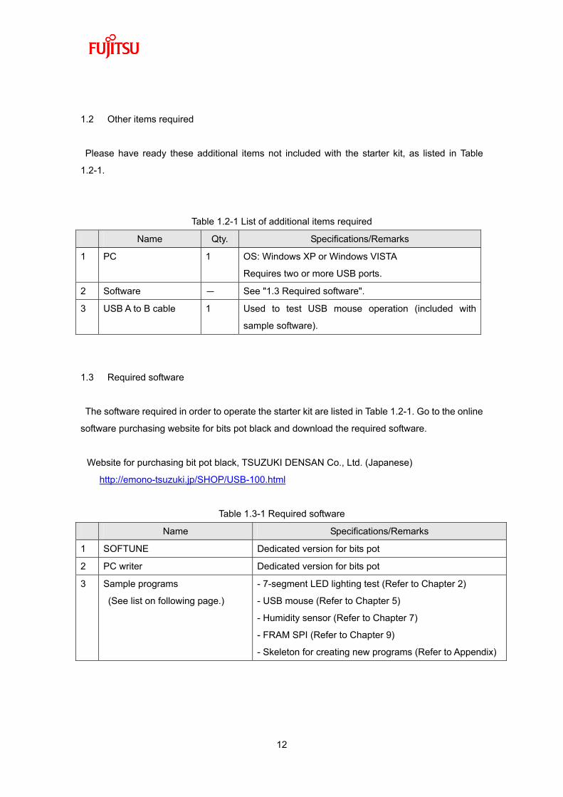
1.2 Other items required
Please have ready these additional items not included with the starter kit, as listed in Table
1.2-1.
Table 1.2-1 List of additional items required
Name Qty. Specifications/Remarks
1 PC 1 OS: Windows XP or Windows VISTA
Requires two or more USB ports.
2 Software - See "1.3 Required software".
3 USB A to B cable 1 Used to test USB mouse operation (included with
sample software).
1.3 Required software
The software required in order to operate the starter kit are listed in Table 1.2-1. Go to the online
software purchasing website for bits pot black and download the required software.
Website for purchasing bit pot black, TSUZUKI DENSAN Co., Ltd. (Japanese)
http://emono-tsuzuki.jp/SHOP/USB-100.html
Table 1.3-1 Required software
Name Specifications/Remarks
1 SOFTUNE Dedicated version for bits pot
2 PC writer Dedicated version for bits pot
3 Sample programs
(See list on following page.)
- 7-segment LED lighting test (Refer to Chapter 2)
- USB mouse (Refer to Chapter 5)
- Humidity sensor (Refer to Chapter 7)
- FRAM SPI (Refer to Chapter 9)
- Skeleton for creating new programs (Refer to Appendix)

13
The sample programs are organized as shown in the diagram below.
(The sample program provided by INTERFACE Co., Ltd., is beyond the scope of this manual.)
[bits_pot_black_e]
[sample_program]
sample_program_e.zip : Sample programs
[monitor]
moitor.mhx : Monitor programs
[manual]
users_manual_e.pdf : User's manual (Instruction manual)
schematic.pdf : Schematic diagrams
[software]
[SOFTUNE]
FR_ProPack_Rev600010-BV-ComExpansion.zip : Dedicated version of
SOFTUNE for bits pot
[PC_writer]
MB91F662_setup.exe : Dedicated PC writer for bits pot black

14
1.4 External appearance of the starter kit board and major components
Figure 1.4-1 shows the external appearance of the starter kit board, and Table 1.4-1 lists the
major components.
Figure 1.4-1 External appearance of the starter kit board
(2) FRAM
(1) Main MCU
(5) 7-segment LED
(14) 4 MHz
oscillator
(11) USB Mini-B connector
(9) Slider SW
(for analog input) (4) Terminal block
(3) Humidity sensor (12) USB
B connector
(6) Pushbutton SW (7) Pushbutton SW
(8) Pushbutton SW
(10) Slider SW
(13) USB
A connector

15
Table 1.4-1 Major components on the starter kit board
Component Description Reference
(1) Main MCU FUJITSU 32-bit Microcontroller
MB91F662 (certified USB)
―
(2) FRAM FUJITSU MB85RS256 Chapters 10, 11
(3) Humidity sensor Measures humidity. Chapter 9
(4) Terminal block Connects to plastic board (mounted with strain
gauge) to make an electronic scale.
Chapter 7
(5) 7-segment LED Displays the operating results of sample
programs.
Chapter 2, etc.
(6) Pushbutton SW Used to control the USB mouse operation. Chapter 5
(7) Pushbutton SW Used to control the USB mouse operation.
Used to reset the electronic scale.
Used to control the counter value and operation.
Chapter 5
Chapter 7
Chapters 10, 11
(8) Pushbutton SW Used during debug. Chapter 2
(9) Slider SW
(For analog input)
Used to control the USB mouse operation. Chapter 5
(10) Slider SW Controls mode selection of the main
microcontroller.
Chapter 2
Appendix
(11) USB Mini-B
connector
Connects the PC and main microcontroller with
the USB B to Mini-B cable. Used for debugging
serial communications.
Chapter 2
(12) USB B connector Used to control the USB mouse operation. Chapter 5
(13) USB A connector Used when operating the microcontroller as a
host. This usage is not described in this manual.
―
(14) 4 MHz oscillator Generates the main clock for the sample
programs.
―

16
1.5 Starter kit parts
Table 1.5-1 lists the parts in the starter kit.
Table 1.5-1 Starter kit parts
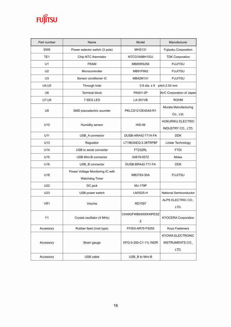
Part number Name Model Manufacturer
C1,C2,C4,C6,C9,
C10,C12,C13,
C18,C19,C37,
C36,C56,C58,
C60,C61
Monolithic ceramic capacitor 0.1uF GCM188R11E104KA42DMurata Manufacturing
Co., Ltd.
C3,C5 Monolithic ceramic capacitor 18pF GCM1552C1H180JZ0DMurata Manufacturing
Co., Ltd.
C7,C11,C54,C55 Monolithic ceramic capacitor 4.7uF GCM31CR71E475KA40LMurata Manufacturing
Co., Ltd.
C17,C32,C33 Monolithic ceramic capacitor 10uF GCM32ER71E106KA42LMurata Manufacturing
Co., Ltd.
C14,C15,C16 Monolithic ceramic capacitor 47000pF GCM155R11A473KA01DMurata Manufacturing
Co., Ltd.
C20,C21,C22,
C23,C24,C25,
C26,C27,R87,R88
Monolithic ceramic capacitor 470pF GCM1552C1H471JA0DMurata Manufacturing
Co., Ltd.
C28,C29 Monolithic ceramic capacitor 47pF GCM1552C1H470JA0DMurata Manufacturing
Co., Ltd.
C35 Monolithic ceramic capacitor 10000pF GCM155R11E103KA01DMurata Manufacturing
Co., Ltd.
C57 Monolithic ceramic capacitor 22000 pF GCM155R11E223KA01DMurata Manufacturing
Co., Ltd.
C59 Monolithic ceramic capacitor 150uF F911A157MNC Nichicon
D2,D3,D4,D5,D6,D7 LED SML-210LT ROHM
D10,D11 Diode 1SR154 ROHM
L1,L3,L4 Chip beads MPZ2012S300AT TDK Corporation
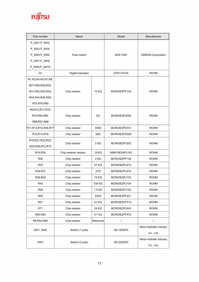
17
Part number Name Model Manufacturer
P_SW1,P_SW2,
P_SW3,P_SW4,
P_SW5,P_SW6,
P_SW7,P_SW8,
P_SW9,P_SW10
Push switch B3S-1000 OMRON Corporation
Q1 Digital transistor DTA114TUA ROHM
R1,R3,R4,R5,R7,R8,
R27,R28,R29,R30,
R31,R32,R33,R34,
R42,R44,R45,R49,
R70,R76,R89
Chip resistor 10 KΩ MCR03EZPF103 ROHM
R9,R10,R17,R78,
R79,R84,R85,
R86,R87,R88
Chip resistor 0Ω MCR03EZPJ000 ROHM
R11,R13,R15,R26,R77 Chip resistor 330Ω MCR03EZPD331 ROHM
R12,R14,R16 Chip resistor 20Ω MCR03EZPD200 ROHM
R18,R21,R22,R23,
R25,R39,R72,R75 Chip resistor 2 KΩ MCR03EZPJ202 ROHM
R19,R24 Chip network resistor 18 KΩ MNR18E0APJ182 ROHM
R20 Chip resistor 2 KΩ MCR03EZPF102 ROHM
R35 Chip resistor 47 KΩ MCR03EZPJ473 ROHM
R36,R37 Chip resistor 27Ω MCR03EZPJ270 ROHM
R38,R40 Chip resistor 15 KΩ MCR03EZPJ153 ROHM
R43 Chip resistor 100 KΩ MCR03EZPJ104 ROHM
R48 Chip resistor 1.5 KΩ MCR03EZPJ152 ROHM
R50 Chip resistor 220Ω MCR03EZPF221 ROHM
R51 Chip resistor 51 KΩ MCR03EZPF513 ROHM
R71 Chip resistor 24 KΩ MCR03EZPJ243 ROHM
R80,R83 Chip resistor 4.7 kΩ MCR03EZPF472 ROHM
R6,R52,R90 Chip resistor Reserved ― ―
SW1, SW2 Switch (1 pole) SS-12SDP2 Nihon Kaiheiki Industry
Co., Ltd.
SW3 Switch (2 pole) SS-22SDP2 Nihon Kaiheiki Industry
Co., Ltd.
18
Part number Name Model Manufacturer
SW6 Power selector switch (3 pole) MHS131 Fujisoku Corporation
TE1 Chip NTC thermistor NTCG164BH103J TDK Corporation
U1 FRAM MB85RS256 FUJITSU
U2 Microcontroller MB91F662 FUJITSU
U3 Sensor conditioner IC MB42M131 FUJITSU
U4,U5 Through hole 0.8 dia. x 9 pitch:2.54 mm
U6 Terminal block PA001-2P AVC Corporation of Japan
U7,U9 7-SEG LED LA-301VB ROHM
U8 SMD piezoelectric sounder PKLCS1212E40A0-R1 Murata Manufacturing
Co., Ltd.
U10 Humidity sensor HIS-06 HOKURIKU ELECTRIC
INDUSTRY CO., LTD.
U11 USB_A connector DUSB-ARA42-T11A-FA DDK
U13 Regulator LT1963AEQ-3.3#TRPBF Linear Technology
U14 USB to serial converter FT232RL FTDI
U15 USB Mini-B connector 54819-0572 Molex
U16 USB_B connector DUSB-BRA42-T11-FA DDK
U18 Power Voltage Monitoring IC with
Watchdog Timer MB3793-30A FUJITSU
U22 DC jack MJ-179P
U23 USB power switch LM3525-H National Semiconductor
VR1 Volume RD7097 ALPS ELECTRIC CO.,
LTD.
Y1 Crystal oscillator (4 MHz) CX49GFWB04000H0PESZ
Z KYOCERA Corporation
Accessory Rubber feed (rivet type) FF003-AR79 P3055 Koyo Fasteners
Accessory Strain gauge KFG-5-350-C1-11L1M2R
KYOWA ELECTRONIC
INSTRUMENTS CO.,
LTD.
Accessory USB cable USB_B to Mini-B

19
1.6 Power supply methods
There are three methods for supplying power to the board, each selected using SW6 as shown
below. The Power LED lights up red when power is supplied.
Power supply Silk printing on board Remarks
1 USB Mini-B
connector
USB Mini-B Draws bus power from the PC via the USB
A to Mini-B cable.
2 USB B connector USB FUNC Draws bus power from the PC via the USB
A to USB B cable.
3 External power
supply (5V)
External Draws power from an AC adapter. (AC
adapter not included with kit.)
< Typical AC adapter models>
Model No: GF12-US0520
I/P: 100-240V 50/60Hz 0.3A
O/P: DC 5V 2.0A

20
!! Caution !!
• Do not change the power supply selector switch while the microcontroller is operating.
• Never change the power supply selector to External when the external power supply (5V) is
not supplying power.
• Do not change the power supply selector switch to USB FUNC when the USB B connector
is disconnected.
• Do not change the power supply selector switch to USB Mini-B when the USB Mini-B
connector is disconnected.
1. via USB Mini-B connector
3. External power supply (5V)
2. via USB B connector
Power supply selector SW
Lights up when power is ON

21
2 Setting up the PC
Install the software required to operate this starter kit to your PC.
Be sure to download the required software before starting the installation process.
The setup procedures are as follows.
Setup procedures:
- Installation of the integrated development environment SOFTUNE (bits pot dedicated version)
(Refer to Section 2.1)
- Installation of USB drivers (Refer to Section 2.2)

22
2.1 Installing the integrated development environment SOFTUNE (bits pot dedicated version)
What is SOFTUNE?
SOFTUNE is the integrated development environment (IDE) for developing programs and
evaluating FUJITSU Microcontrollers. Developing programs for microcontrollers commonly used
in embedded devices is a repetitive cycle of coding the source, building the executable, checking
program operation (debug), and reflecting the debug results into the source code again. The
SOFTUNE IDE is a tool designed to support the development process by integrating these tasks
into a seamless systematic flow.
!! Caution !!
If the product version of SOFTUNE V6 is already installed on your PC, uninstall it and then
re-install the SOFTUNE version dedicated for bits pot.
The installation procedures for SOFTUNE (bits pot dedicated version) are described below.
Unpack the downloaded files "FR_ProPack_Rev600010-BV.zip(*)" to a folder on your PC.
After the files are unpacked, double-click on "setup.exe". The setup window welcome screen
appears. Follow the instructions in the window to begin the installation.
(*) bits_pot_black/software/SOFTUNE/FR_ProPack_Rev600010-BV-ComExpansion.zip
(This explanation is described using Windows XP screens.)
Click "OK".

23
Click "Next".
Click "Next".

24
If you agree with the usage license, click "Yes".
Click "Next".

25
Click "Next". Leave the destination folder at the default, "C:¥Softune6".
Confirm the components selected for installation. "Customize Bar" is not checked by default so
place a check in it.

26
Verify the details of the installation are acceptable.
If there are no problems, click "Next".
Wait for the installation to complete.

27
Click the "Finish" button to complete the installation of SOFTUNE.

28
2.2 Installing the USB driver
The starter kit is equipped with a USB-to-serial converter IC (made by FTDI) between the USB
Mini-B connector and microcontroller. This USB driver must be downloaded from the FTDI
website.
Download the driver software to a folder on your PC from the URL listed below beforehand.
FTDI (Future Technology Devices International Ltd.)
Virtual COM Port Drivers
http://www.ftdichip.com/Drivers/VCP.htm
The driver can be downloaded from here.
The version number as of September 2008 is "2.04.06".
29
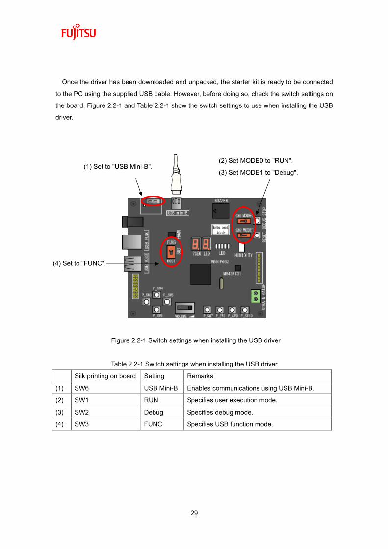
Once the driver has been downloaded and unpacked, the starter kit is ready to be connected
to the PC using the supplied USB cable. However, before doing so, check the switch settings on
the board. Figure 2.2-1 and Table 2.2-1 show the switch settings to use when installing the USB
driver.
Figure 2.2-1 Switch settings when installing the USB driver
Table 2.2-1 Switch settings when installing the USB driver
Silk printing on board Setting Remarks
(1) SW6 USB Mini-B Enables communications using USB Mini-B.
(2) SW1 RUN Specifies user execution mode.
(3) SW2 Debug Specifies debug mode.
(4) SW3 FUNC Specifies USB function mode.
(1) Set to "USB Mini-B". (2) Set MODE0 to "RUN".
(3) Set MODE1 to "Debug".
(4) Set to "FUNC".

30
After setting the switches on the board, connect the PC and board using the USB A to Mini-B
cable supplied with the starter kit.
When you connect the board to the PC, the PC will recognize the new hardware and display
messages prompting you to install the driver. Follow these steps to install the driver.
Do not connect the cable to
"USB FUNC" or "USB HOST".
To USB Mini-B connector

31
This procedure will explain how to install the driver software previously downloaded instead of
connecting to Windows Update.
Select "Install from a list or specific location (Advanced)", and click "Next".
Click "Browse" and specify the folder "CDM 2.04.06 WHQL Certified" downloaded earlier, then
click "Next".
32
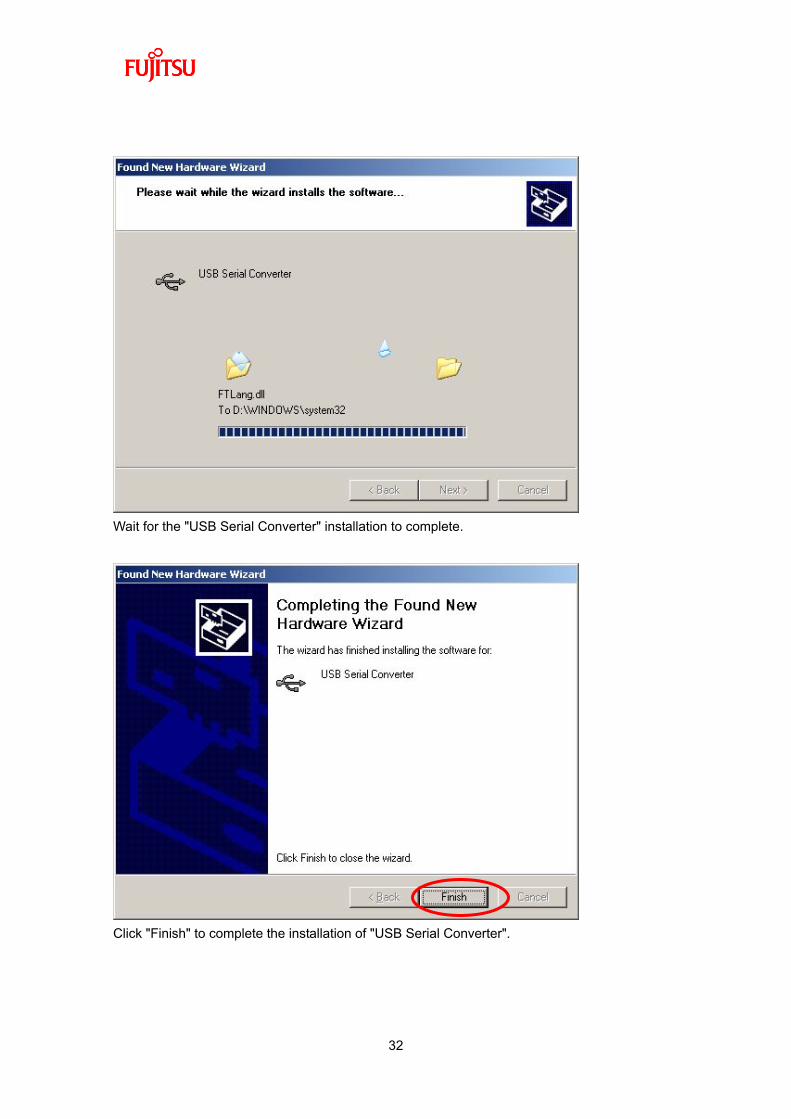
Wait for the "USB Serial Converter" installation to complete.
Click "Finish" to complete the installation of "USB Serial Converter".

33
Next, install the "USB Serial Port".
Select "Install from a list or specific location (Advanced)", and click "Next".
Click "Browse" and specify the folder "CDM 2.04.06 WHQL Certified" downloaded earlier, then
click "Next".

34
Wait for the "USB Serial Port" installation to complete.
Click "Finish" to complete the installation of "USB Serial Port".
This completes the installation of the USB driver.

35
3 Launching SOFTUNE and using the monitor debugger
3.1 Launching SOFTUNE
After installing SOFTUNE and the USB driver, launch SOFTUNE by clicking Windows [Start] -
[All Programs] - [SOFTUNE V6] - [FR Family SOFTUNE Workbench].
Figure 3.1-1 shows the screen layout when SOFTUNE starts up.
Figure 3.1-1 Screen layout at SOFTUNE startup
The SOFTUNE window is comprised of a menu bar, tool bar, project window, edit window,
output window, and status bar.
Project
window
Edit window
Output window
Status bar
Tool bar Menu bar

36
Menu bar Contains menu items for the SOFTUNE application.
Tool bar The tool bar has groups of buttons for frequently used
commands. You can move the tool bar anywhere on the screen
by clicking inside the group frame with the left mouse button and
dragging it.
Project window Displays a tree view of the name of the currently open project
and the files registered to the project.
Edit window This is the window used to display and edit source files.
Output window This window shows version information and error messages
generated by the compiler during the make and build process.
Status bar The status bar shows the current status of SOFTUNE.
!! HINT !!
You can move the position of the tool bars and resize windows freely to match your
preferences.
Project
window Edit window
Output window
Grab the edge of the tool bar to move it.

37
Unpack the downloaded sample programs.
Open "sample.wsp (*)". From the "File (F)" menu, click "Open (O)", select "Workspace/project
file", then select "sample.wsp" and click OK.
(*) bits_pot_black/sample_program/project/sample.wsp
!! HINT !!
You can also open a workspace file by dragging and dropping the "sample.wsp" file from
Explorer onto the SOFTUNE window.
When "sample.wsp" opens, a tree view showing the registered projects in the sample
programs appears in the project window. Table 3.1-1 shows the projects in the workspace.
Figure 3.1-2 Contents of "sample.wsp"
Table 3.1-1 List of projects in sample.wsp
Project name Description Reference
io_mb91660 CPU register definitions file ―
sample_LED 7-segment LED program Chapter 2 (this chapter)
sample_skeleton For creating new programs Appendix
sample_USB USB mouse Chapter 5
sample_humidity Hygrometer Chapter 9
sample_strain_gauge Electronic scale Chapter 7
sample_FRAM_SPI Counter using FRAM Chapter 11

38
In order to confirm everything has been setup properly, we will use the sample program
"sample_LED" to flash the letters "FJ" on the 7-segment LED on the starter kit board.
Make sure "sample_LED.abs – “sample_LED.prj”[Debug]” is set as the active project and
appears in bold type.
!! Caution !!
The active project is the target project for the compiler and debugging. To execute other
sample programs explained after this Chapter, make sure the project is set as the active
project.
To set a project as the active project, right-click on the project in the project window and click
"Set as Active Project". The active project appears in bold type.
Click the + next to "Source Files" and check the registered files. Double-click the file name to
view it in the edit window

39
Next, we will compile the program.
Click the "Build" button to compile, and verify there were no errors in the compilation results in
the output window.
If the compilation was successful, proceed to setup and launch the monitor debugger.
"Build" button

40
3.2 Setting and launching the monitor debugger
Explanation of the monitor debugger
The monitor debugger allows developers to debug the program loaded on a production
microcontroller with built-in FLASH memory. Installing a monitor program with the application
program provides access to debug functions. (Read also the monitor debugger explanation
given in the Appendix at the end of the manual.)
Click the + next to "Debug" to setup the monitor debugger. Right-click on "sample_LED.sup"
and select "Change settings" to launch the setup wizard for the debugger.
41
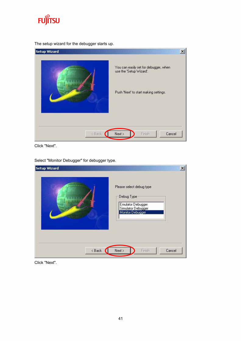
The setup wizard for the debugger starts up.
Click "Next".
Select "Monitor Debugger" for debugger type.
Click "Next".

42
Select "RS" as the Type and specify the COM port the board is connected to. Leave the baud
rate at "256000".
Click "Next".
Refer to Appendix 2 in this manual to
verify COM ports.

43
Click "Next".
Make sure the option "Auto load when starting debug." has a check in it, and that the batch file
for "Before" is set to "FshLdWrt.prc".
"FshLdWrt.prc" is a batch file for writing user programs to the FLASH memory on the board.
Check the settings and click "Finish" to complete the setup wizard.
44
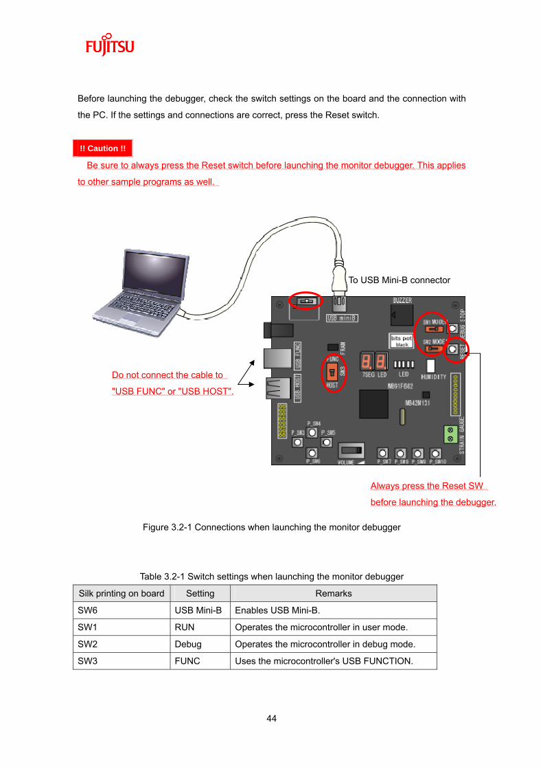
Before launching the debugger, check the switch settings on the board and the connection with
the PC. If the settings and connections are correct, press the Reset switch.
!! Caution !!
Be sure to always press the Reset switch before launching the monitor debugger. This applies
to other sample programs as well.
Figure 3.2-1 Connections when launching the monitor debugger
Table 3.2-1 Switch settings when launching the monitor debugger
Silk printing on board Setting Remarks
SW6 USB Mini-B Enables USB Mini-B.
SW1 RUN Operates the microcontroller in user mode.
SW2 Debug Operates the microcontroller in debug mode.
SW3 FUNC Uses the microcontroller's USB FUNCTION.
Do not connect the cable to
"USB FUNC" or "USB HOST".
To USB Mini-B connector
Always press the Reset SW
before launching the debugger.

45
From the SOFTUNE "Debug" menu, select "Start debug".
If the settings were made correctly, the batch file for "Before " in the setup wizard will run.
When the dialog bar is showing, the program is being downloaded to the FLASH memory on the
microcontroller. Do not disconnect the USB cable from the board or the PC during the download.

46
If the debugger does not launch
Check the following.
1. Board settings.
• Is the USB cable properly connected to the board and PC?
• Are the switches on the board set properly?
2. Setup wizard settings.
• Are the COM port and baud rate settings correct?
3. If both 1 and 2 are correct but the debugger still does not launch, the monitor program may
be corrupt. Refer to Appendix 3 to write the monitor program using the PC Writer, and then
launch the debugger.

47
3.3 Using the monitor debugger
The debugger will launch when the download to the FLASH memory on the microcontroller
completes. The debugger should be pointing to the starting address of the user program.

48
Run the program by clicking the "Run continuously" button in the upper left of the SOFTUNE
window.

49
Execution is successful if the letters "FJ" appear flashing on the 7-segment LED.

50
To stop program execution, press the "DEBUG STOP" button on the board. The flashing "FJ" will
stop when the DEBUG STOP button is depressed. Depending on the timing, the program may
stop with FJ still showing.
To resume program execution, click "Run Continuously" in the upper left of the SOFTUNE
window.
In addition to running continuously, SOFTUNE also allows "Step Execution" and "Run to Cursor".
The basic functions in SOFTUNE are listed below.
Program stops by pressing
DEBUG STOP

51
Function Description
(1) Run Continuously Executes program continuously from the current position in the
program counter (PC).
(2) Step In Executes the step and moves the PC to the address of the next
instruction and stops.
(3) Step Over Executes the step and moves the PC to the beginning of the next
instruction and stops.
(4) Step Out Executes to the end of the current function, returns to the caller
function, moves the PC to the address of the next instruction, and
stops.
(1),(2),(3),(4) (5),(6) (7)
(8),(9)
(10)

52
(5) Make Compiles/assembles only the source files that have changed. Then,
links all objects and libraries to generate the target program.
(6) Build Compiles/assembles all source files registered in the project, whether
they have changed or not, then links all objects and libraries to
generate the target file.
(7) Customize Bar This function allows you to register a shortcut to a batch file, or a
Workbench menu item, that can be used while the debugger is
running.
This starter kit comes with a batch file that "returns to the starting
address of the user program". You can register and use this function
by registering start.prc by referring to "(4) Customize Bar" under
"Appendix 1. Creating projects/sample programs as new projects".
(8) Run to Cursor
Executes the instructions up to the address where the cursor is,
moves the PC to the address of the cursor, and stops.
(9) Break Point Places an x mark where you wish to stop the program.
(10) Mix display Right-click on the program showing in the debug window and select
"Mixed display" from the popup menu. A check next to "Mixed display"
will show the source code in both C language and reverse assembler
code.
- Stop To stop a continuously running program, press the "DEBUG STOP"
button on the board.

53
(11) Memory window Shows the memory contents during debug. If the window is not
showing, click "View" - "Memory" to show it.
(12) Register window Shows the register contents during debug. If the window is not
showing, click "View" - "Register" to show it.
(13) Watch window Displays a tree view of the specified variable values. If the
window is not showing, click "View" - "Watch" to show it. There
are four types of watch windows available. The windows can be
shown or hidden by categorizing and registering variables to
each window.
(11) (12) (13)

54
3.4 Exiting monitor debug
To end debugging, always stop the program execution by pressing the DEBUG STOP button
on the board . Then, click "Debug" - "End Debug".
Refer to the monitor debugger limitations provided in the Appendix.

55
4 What is a USB?
4.1 What is a USB?
USB stands for Universal Serial Bus.
In 1993, engineers from Compaq, Intel, Microsoft, and NEC gathered and jointly developed a
peripherals interface for next-generation PCs. This led to their release of the first USB 1.0
specifications (standards) in 1996. USB 1.1 was released in 1998 and USB 2.0 was released in
2000. For many years, the RS-232C and printer ports served as the main interface for
connecting peripherals to a PC. The problem with these legacy interfaces was that they were
limited to low transfer rates, allowed only one device to be connected per port, and thus required
an increase in ports to connect more devices.
This lead to an extensive array of connectors occupying the rear panels of PCs, including
separate ports for the keyboard, mouse, and display. The USB was developed to consolidate
these interfaces into a single connector that would allow connection of various peripherals.
4.2 Features of the USB
The USB has these features.
1. Ease of use
USB supports Plug-and-play and Hot Swapping, and Bus Power, making it easy to expand
PC peripherals and communicate between embedded devices.
Plug-and-play refers to the mechanism for automatically recognizing a device and installing
the proper driver when it is plugged in to the PC.
Hot Swapping is a general reference to the ability of plugging or unplugging devices with the
PC power still on. That is, the PC power does not have to be turned off or rebooted during or
after the device is plugged or unplugged.
Bus Power refers to the standard for supplying from the PC via the cable. (The opposite of
this is referred to as "Self-powered".)
2. Single master system
USB follows the single master system for transferring data.
We will explain using the PC as an example. The peripherals to a PC are controlled by the PC
(host), and data is exchanged between the peripheral and the host. Peripherals cannot transfer
data directly to another host. Furthermore, a peripheral cannot request a data transfer to the host.
The peripheral must perform data transfers at the request of the host. Because there is only one

56
host in each of these examples, the system is called a single master system.
Today, printers and digital cameras are also equipped with USB, not just the PC.
These devices can transfer data between themselves without going through a host PC using a
hosting function called USB Mini-Host.
The MB91F662 installed on this board is equipped with the Mini-Host function.
3. Signal lines
USB cables are inexpensive to make, using only two signal lines and two power lines.
The two signal lines carry 3.3 V differential signals (D+ and D-). The two power lines are
labeled Vbus (5V), and GND. Connected devices can draw up to 500 mA of power, allowing
manufacturers to develop devices that do not require external power supplies.
(This board can supply power from the USB.)
Plug types are discussed in Section 4.4.
4.3 Connection formats
The three functions explained here form a USB system.
<Host>
PCs are equipped with the host function as shown in Figure 4.3-1.
The number of devices (or functions), including the hub, that can be connected to a single host
is 127. (The hub is treated as a function.)
<Hub>
The hub is used mainly to increase the number of ports. With PCs, some monitors and
keyboards are equipped with USB hubs.
<Function>
Functions are provided on the peripheral. In a PC, the keyboard and mouse are functions.
The host and function are connected in a so-called star topology, which means simply that
functions are directly connected to the host via a hub for communicating on a 1:1 basis.

57
Figure 4.3-1 USB Connection Example
4.4 Plug
Each end of the USB has a plug with a different shape. One end is called the A plug, the other
the B plug. A smaller connector is used on embedded devices and is called a Mini-A plug and
Mini-B plug, to distinguish from the standard plug size. The cable supplied with this board has an
A plug and a Mini-B plug.
The USB device on a host is always equipped with an A plug. The plugs are shaped differently
to prevent incorrect insertion.
Figure 4.4-1 USB connector shapes used on this board
Figure 4.4-2 Relation between connections and connectors
PC
(Host)
Keyboard
Mouse
Hub
Printer
Web camera
Digital camera
USB memory
Hub
A plug B plug Mini-B plug
Host A
A
A
B Function
B Function
B Hub A
A B Function
B Function

58
4.5 Transfer rate
USB transfer rates are standardized as shown below.
Table 4.5-1. USB Transfer rates
Low Speed Full Speed High Speed
USB 1.0/1.1 1.5 Mbps 12 Mbps -
USB 2.0 1.5 Mbps 12 Mbps 480 Mbps
The MB91F662 supports only Full Speed.
4.6 Transfer rate detection
The USB standard requires that USB devices allow for the automatic detection of their data
transfer rate when connected to the host by using a pull-up resistor.
- A Full Speed device pulls up the D+ signal line with a 1.5 kΩ (R2) resistor.
- A Full Speed device pulls up the D- signal line with a 1.5 kΩ (R2) resistor.
(Transfer rate types will be discussed later.)
After the USB device is connected, the host detects whether it is the D+ signal line or D- signal
line that is pulled up, and selects its data transfer rate accordingly.
Additionally, cable lengths are standardized to a maximum of 5 meters for Full Speed rates, and
a maximum of 3 meters for Low Speed rates.
Figure 4.6-1 Differences in connection based on transfer rates

59
4.7 Transfer methods
Several transfer methods are specified for the USB.
Table 4.7-1 below summarizes the USB transfer methods.
Table 4.7-1 USB transfer methods
Isochronous transfer Interrupt transfer Bulk transfer Control transfer
Typical
application
This is the most preferred transfer method for the USB. This transfer method has a guaranteed bandwidth and is used where real-time transfers are required, such as audio equipment, telephones, etc.
A feature of this method is that the delay time is guaranteed, thus requiring quick responses. Keyboards, game pads or consoles use this transfer method.
This method is used with devices that transfer large volumes of data, such as printers, scanner, digital cameras.
This method is used to send and receive configurations and messages from the USB device.
< Transfer rates>
12 Mbps
(Full Speed) Supported Supported Supported Supported
1.5 Mbps
(Low Speed) Not supported Supported Not supported Supported
< Data transfer volume per packet>
12 Mbps
(Full Speed) 1 to 1023 bytes 1 to 64 bytes 1 to 64 bytes 1 to 64 bytes
1.5 Mbps
(Low Speed) Not supported 1 to 8 bytes Not supported 1 to 8 bytes
< Transfer direction>
Host ->
Function Supported
Function ->
Host Supported
Retry request
for data errors None Yes

60
4.8 Configuration of a device
The host communicates by specifying addresses and endpoint numbers that it assigns to each
USB device.
When the USB device is connected, the host assigns a unique address to each function and
hub. At the beginning of the connection, the device is always assigned to address "0". Thereafter,
the host assigns an address from 1 to 127. Each function and hub has several buffers for
transferring data over the USB called endpoints. A full speed device can have up to 16 endpoints,
while a low speed device can have up to three. Each endpoint is defined with an endpoint
number, transfer direction, transfer method, and maximum packet size. Each definition uses a
specific endpoint. All USB devices must have endpoint 0 to support control transfers.
Figure 4.8-1 Addresses and endpoint numbers

61
4.9 Enumeration
Enumeration refers to the process that begins by the host recognizing the device connected to
the bus, specifying an address, and fixating the descriptor information received from the device.
The USB device uses the descriptor to inform the host of its attributes. There are several types of
descriptors that the host can request. In turn, the device returns information that describes itself
to the host. The USB device is ready to be used by the host when it has been assigned an
address and its configuration has been recognized. (Refer to Figure 6 below)
Figure 4.9-1 Enumeration

62
USB transmissions are managed by dividing time into frames that repeat every 1 ms, and
allocating small portions of this transmission time to each device within each frame. The host
starts a frame by sending the SOF packet every 1 ms. This is followed by a token packet sent
from the host, which informs the device of the transfer type, device address, and end point.
Devices may respond to the data and handshake packet only if they have been addressed.
The ACK packet is issued when the data transfer completes, while the NAK packet is issued
when no endpoints are available (requesting the host to resend). STALL is issued when the
endpoint cannot be used.
Figure 4.9-2 Frames

63
The packets shown in Figure 4.9-3 are combined to form a frame for transferring over the USB.
Each packet will be explained.
All packets begin with a SYNC field. This is an 8-bit field used to synchronize the input data and
local clock on the input circuit. The SYNC field is used only for synchronizing. The frame starting
packet contains an SOF (Start of Frame) field after the SYNC field.
SOF is a type of PID (Packet ID), but used only for the frame starting packet. The Frame
Number field is for counting the number of frames.
The CRC (Cyclic Redundancy Check) field is used to detect transmission errors.
An EOP (End of Packet) is sent at the end of each packet.
In the token packet, the PID is followed by a 7-bit address and 4-bit endpoint number, plus a
5-bit CRC for detecting transmission errors.
In the data packet, the PID is followed by a 16-bit CRC for detecting transmission errors.
The side that receives the data sends a handshake packet.
Figure 4.9-3 USB packet format

64
Table 4.9-1 shows the PID types (which indicates the status of the packet being sent) defined
for USB.
Table 4.9-1 PID types
PID type PID name PID[3:0] Description
OUT 0001b Notification from the host to the function that it is about to send
data.
IN 1001b Notification from the function to the host that it is about to send
data.
SOF 0101b Notifies the start of a frame.
Token
SETUP 1101b Notification for starting control transfer.
DATA0 0011b Data packet (even) Data
DATA1 1011b Data packet (odd)
ACK 0010b Notification that the data packet was successfully received.
NAK 1010b Notification that the data packet was not received successfully,
or is unable to communicate. Handshake
STALL 1110b Notification that the specified endpoint has an error, and that
action is required of the host.
Special* PRE 1100b Notification that the host is about to start Low Speed transfer.
* Not supported by the MB91F662.
4.10 Device class
In the USB standard, devices that have common functionality, and that are capable of using the
same driver are defined as a device class. Examples of device classes are printers, monitors,
hubs, memory devices (HAD and USB memory devices). Mice and keyboards are defined as an
HID (Human Interface Device) even though they don't have the same number of keys, because
they have the same functionality. This allows developers to develop new devices for a given
device class without developing a new device driver.

65
5 Let's make a USB mouse
This sample program will provide USB communications that a USB mouse uses (HID class) by
utilizing the USB function controller in the microcontroller (MB91F662) installed on the starter kit.
When the starter kit board is connected to the PC, the PC will recognize the board as a USB
mouse (HID class). Operating the pushbutton switches and slider switch on the board will
simulate the operation of a mouse.
5.1 Overview of the USB sample program
This sample program simulates a USB mouse (HID device) on the MB91F662. Figure 5.1-1
shows the operation and details of the sample program. When the starter kit board running the
sample program is connected to the PC, the PC recognizes the MB91F662 on the board as a
USB mouse (HID device). After the PC completes the connection and recognition process, the
pushbuttons on the board can be used to move the cursor or perform click operations on the
PC screen. The slider switch on the board can be used to scroll windows on the PC. The
program periodically scans the pushbuttons and slider switch to detect these status changes.
66
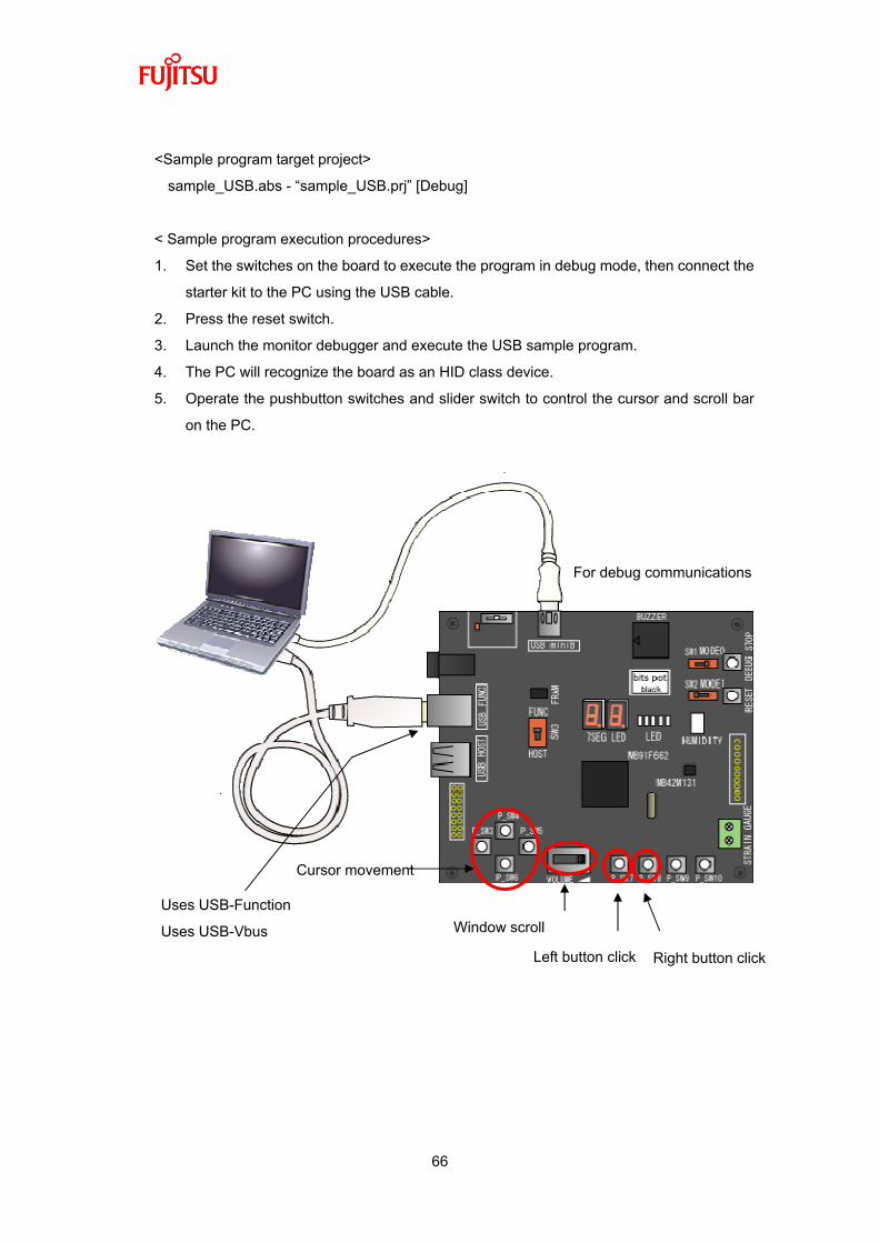
<Sample program target project>
sample_USB.abs - “sample_USB.prj” [Debug]
< Sample program execution procedures>
1. Set the switches on the board to execute the program in debug mode, then connect the
starter kit to the PC using the USB cable.
2. Press the reset switch.
3. Launch the monitor debugger and execute the USB sample program.
4. The PC will recognize the board as an HID class device.
5. Operate the pushbutton switches and slider switch to control the cursor and scroll bar
on the PC.
Left button click
Cursor movement
Window scroll
Right button click
For debug communications
Uses USB-Function
Uses USB-Vbus

67
Part name Silk printing on
board
Description
Pushbutton SW P_SW3 Moves PC cursor left
Pushbutton SW P_SW4 Moves PC cursor up
Pushbutton SW P_SW5 Moves PC cursor right
Pushbutton SW P_SW6 Moves PC cursor down
Pushbutton SW P_SW7 Left button click
Pushbutton SW P_SW8 Right button click
Slider SW VR1 Slide volume left to scroll up, slide to right to scroll down
USB port USB FUNC Uses USB-Function, USB-Vbus pins (PH3)
Figure 5.1-1 Operation and details of the USB sample program

68
5.2 Overview of USB communications flow
This section explains the USB communications flow performed by the sample program. Details
on the USB communications protocol have been omitted. Refer to the USB and HID class
specifications for details.
5.2.1 Overview of USB communications flow
This sample program provides communications with the PC (USB host) as shown in the
following flow diagrams. Figures 5.2.1-1 and 5.2.1-2 show the configuration process when
the USB is connected. Figure 5.2.1-3 shows an overview of the communications flow after
the USB connection is completed. The -> arrow indicates data is being sent from the PC to
the starter kit (USB Function), and the <- arrow indicates data is being sent from the starter
kit to the PC. The contents of the data will be explained in the next section.

69
Figure5.2.1-1 USB (mouse) communications flow (Configuration 1)
PC (USB host) Starter kit (USB Function)
[EP0]
Get Descriptor (Device) request
Device Descriptor response
Issue bus reset signal
Get Descriptor (Device) request
Device Descriptor response
USB connection (bus connection)
Set Address request
The USB sample program recognizes the USB connection using the V-bus connection terminal (PH3).
0 byte data response
The MB91F662 USB function controller responds to the SET_ADDRESS request automatically at the hardware level.

70
Figure5.2.1-2 USB (mouse) communications flow (Configuration 2)
Set Configuration request
Get Descriptor (Report) request
Report Descriptor response
Get Descriptor (Configuration) request
Configuration Descriptor response Interface Descriptor response HID Class Descriptor response Endpoint Descriptor response
Set Idle request
PC (USB host) Starter kit (USB Function)
[EP0]
The MB91F662 USB function controller responds to the
SET_CONFIGURATION request automatically at the
hardware level.
0 byte data response
0 byte data response

71
Figure5.2.1-3 USB (mouse) communications flow (After configuration)
Notification of Report data
Notification of Report data
:
:
:
:
PC (USB host) Starter kit (USB Function)
[EP1]
Configuration completed (recognizesboard as a USB mouse)
:
:
:
:
Notification of Report data
:
:
The PC (USB host) periodically issues interrupt (IN)
transfer requests. If the status of the USB device
has changed (mouse pointer information, etc.), the
USB device responds with Report data.

72
5.2.2 Device request (PC -> Starter kit)
In this sample program, the data received by the starter kit is called a device request. The
format of data in a device request is standardized. The device requests received by the
starter kit are shown below.
Table 5.2.2-1 Device request (GET_DESCRIPTOR (Device))
Byte Item Description Value
1 bmRequestType Type of request
(Transfer direction: Device -> host / type: standard/ receive:
device : 80h)
80h
1 bRequest Request (GET_DESCRIPTOR: 06h) 06h
00h 2 wValue Requested descriptor type and index value
(Descriptor type (device): 01h) 01h
00h 2 wIndex 0 or language ID
00h
XXh 2 wLength Number of bytes for requested descriptor (YYXXh)
YYh
Table 5.2.2-2 Device request (SET_ADDRESS)
Byte Item Description Value
1 BmRequestType Type of request
(Transfer direction: Host -> device/ type: standard/ receive:
device : 00h)
00h
1 Brequest Request (SET_ADDRESS: 05h) 05h
XXh 2 WValue Device address (address: YYXXh)
YYh
00h 2 WIndex 0
00h
00h 2 WLength 0
00h

73
Table 5.2.2-3 Device request (GET_DESCRIPTOR (Configuration))
Byte Item Description Value
1 BmRequestType Type of request
(Transfer direction: Device -> host / type: standard/ receive:
device : 80h)
80h
1 Brequest Request (GET_DESCRIPTOR: 06h) 06h
00h 2 WValue Requested descriptor type and index value
(Descriptor type (configuration): 02h) 02h
00h 2 Windex 0 or language ID
00h
XXh 2 WLength Number of bytes for requested descriptor (YYXXh)
YYh
Table 5.2.2-4 Device request (SET_CONFIGURATION)
Byte Item Description Value
1 BmRequestType Type of request
(Transfer direction: Host -> device/ type: standard/ receive:
device : 00h)
00h
1 Brequest Request (SET_CONFIGURATION: 09h) 09h
XXh 2 WValue Configuration value (: YYXXh)
YYh
00h 2 Windex 0
00h
00h 2 WLength 0
00h
74
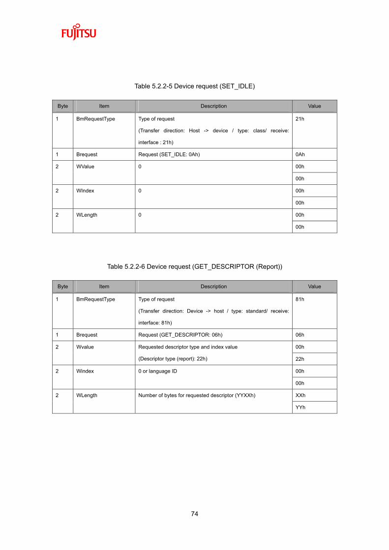
Table 5.2.2-5 Device request (SET_IDLE)
Byte Item Description Value
1 BmRequestType Type of request
(Transfer direction: Host -> device / type: class/ receive:
interface : 21h)
21h
1 Brequest Request (SET_IDLE: 0Ah) 0Ah
00h 2 WValue 0
00h
00h 2 WIndex 0
00h
00h 2 WLength 0
00h
Table 5.2.2-6 Device request (GET_DESCRIPTOR (Report))
Byte Item Description Value
1 BmRequestType Type of request
(Transfer direction: Device -> host / type: standard/ receive:
interface: 81h)
81h
1 Brequest Request (GET_DESCRIPTOR: 06h) 06h
00h 2 Wvalue Requested descriptor type and index value
(Descriptor type (report): 22h) 22h
00h 2 Windex 0 or language ID
00h
XXh 2 WLength Number of bytes for requested descriptor (YYXXh)
YYh
75
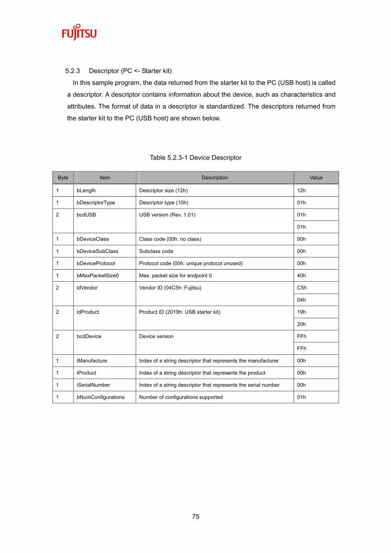
5.2.3 Descriptor (PC <- Starter kit)
In this sample program, the data returned from the starter kit to the PC (USB host) is called
a descriptor. A descriptor contains information about the device, such as characteristics and
attributes. The format of data in a descriptor is standardized. The descriptors returned from
the starter kit to the PC (USB host) are shown below.
Table 5.2.3-1 Device Descriptor
Byte Item Description Value
1 bLength Descriptor size (12h) 12h
1 bDescriptorType Descriptor type (10h) 01h
01h 2 bcdUSB USB version (Rev. 1.01)
01h
1 bDeviceClass Class code (00h: no class) 00h
1 bDeviceSubClass Subclass code 00h
1 bDeviceProtocol Protocol code (00h: unique protocol unused) 00h
1 bMaxPacketSize0 Max. packet size for endpoint 0 40h
C5h 2 idVendor Vendor ID (04C5h: Fujitsu)
04h
19h 2 idProduct Product ID (2019h: USB starter kit)
20h
FFh 2 bcdDevice Device version
FFh
1 iManufacture Index of a string descriptor that represents the manufacturer 00h
1 iProduct Index of a string descriptor that represents the product 00h
1 iSerialNumber Index of a string descriptor that represents the serial number 00h
1 bNumConfigurations Number of configurations supported 01h

76
Table 5.2.3-2 Configuration Descriptor
Byte Item Description Value
1 bLength Descriptor size (09h) 09h
1 bDescriptorType Descriptor type (configuration: 02h) 02h
22h 2 wTotalLength Descriptor size returned for this configuration
(Total size including configuration, interface, HID class, and
endpoint descriptor) 00h
1 bNumInterfaces Number of interfaces supported 01h
1 bConfigurationValue Parameter to pass to Set_Configuration, which is used to select
this descriptor
01h
1 iConfiguration Index of a string descriptor that represents this configuration 00h
1 bmAttributes Device power supply (08h: use bus power) 80h
1 bMaxPower Max. bus current consumption (32h: 100 mA) 32h
Table 5.2.3-3 Interface Descriptor
Byte Item Description Value
1 bLength Descriptor size (09h) 09h
1 bDescriptorType Descriptor type (interface: 04h) 04h
1 bInterfaceNumber 0-based index value used to identify the interface supported by this
configuration
00h
1 bAlternateSetting Value used to select an alternate setting for the interface 00h
1 bNumEndpoints Number of endpoints used by this interface 01h
1 bInterfaceClass Class code (03h: HID class) 03h
1 bInterfaceSubClass Subclass code (01h: supports boot protocol) 01h
1 bInterfaceProtocol Protocol code (02h: mouse) 02h
1 iInterface Index of a string descriptor that represents this interface 00h

77
Table 5.2.3-4 HID Class Descriptor
Byte Item Description Value
1 bLength Descriptor size (09h) 09h
1 bDescriptorType Descriptor type (HID descriptor: 21h) 21h
01h 2 bcdHID HID class version (Ver. 1.01 -> 01h01h)
01h
1 bCountryCode Country identification code (00h: no identification) 00h
1 bNumDescriptors Number of class descriptors 01h
1 bDescriptorType Class descriptor type (22h: HID report) 22h
34h 2 wDescriptorLength Remote descriptor size
00h
Table 5.2.3-5 Endpoint Descriptor
Byte Item Description Value
1 bLength Descriptor size (07h) 07h
1 bDescriptorType Descriptor type (endpoint: 05h) 05h
1 bEndpointAddress Endpoint address (81h: IN direction/EP1) 81h
1 bmAttributes Endpoint attribute (03h: interrupt transfer) 03h
04h 2 wMaxPacketSize Max. packet size for endpoint
00h
1 bInterval Polling interval for endpoint (64h: 100 ms) 64h

78
Table 5.2.3-6 Report Descriptor 1
Byte Item Description Value
05h 2 UsagePage Page usage (Generic Desktop Control)
01h
09h 2 Usage Item usage (Mouse)
02h
A1h 2 Collection Collection item tag (Application)
01h
09h 2 UsagePage Page usage (Pointer)
01h
A1h 2 Collection Collection item tag (Physical)
00h
05h 2 UsagePage Page usage (Button)
09h
19h 2 UsageMinimum Minimum number of items used (1)
01h
29h 2 UsageMaximum Maximum number of items used (3)
03h
15h 2 LogicalMinimum Minimum value the item can report (0)
00h
25h 2 LogicalMaximum Maximum value the item can report (1)
01h
75h 2 ReportSize Data field size to be reported (1 bit)
01h
95h 2 ReportCount Number of data fields to be reported (3)
03h
81h 2 Input Input item tag (Data, Variable, Absolute)
02h
75h 2 ReportSize Data field size to be reported (1 bit)
01h
95h 2 ReportCount Number of data fields to be reported (1)
01h

79
Table 5.2.3-7 Report Descriptor 2
Byte Item Description Value
81h 2 Input Input item tag (Data, Variable, Absolute)
01h
05h 2 UsagePage Page usage (Generic Desktop Control)
01h
09h 2 Usage Item usage (X direction)
30h
09h 2 Usage Item usage (Y direction)
31h
09h 2 Usage Item usage (Wheel)
38h
15h 2 LogicalMinimum Minimum value the item can report (-127)
81h
25h 2 LogicalMaximum Maximum value the item can report (127)
7Fh
75n 2 ReportSize Data field size to be reported (8 bit)
08h
95h 2 ReportCount Number of data fields to be reported (3)
03h
81h 2 Input Input item tag (Data, Variable, Relative)
06h
1 EndCollection EndCollection C0h
1 EndCollection EndCollection C0h
Table 5.2.3-8 HID Device Report Data
Byte Item Description Value
1 Button status Click status of right or left button 0 to 3
1 X axis travel Mouse movement in X axis (horizontal) -127 to 127
1 Y axis travel Mouse movement in Y axis (vertical) -127 to 127
1 Wheel Scroll wheel movement -127 to 127
80
5.3 Sample program sequence
This section describes the operation of the sample program.
5.3.1 Main routine
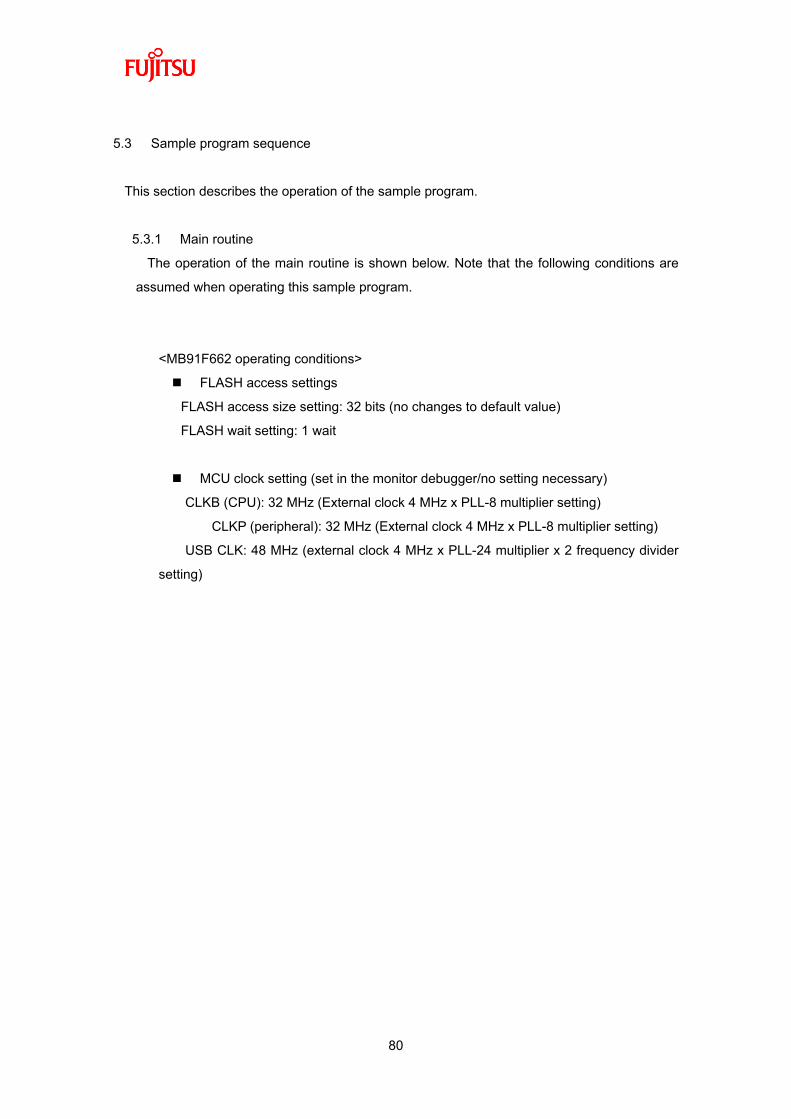
The operation of the main routine is shown below. Note that the following conditions are
assumed when operating this sample program.
<MB91F662 operating conditions>
FLASH access settings
FLASH access size setting: 32 bits (no changes to default value)
FLASH wait setting: 1 wait
MCU clock setting (set in the monitor debugger/no setting necessary)
CLKB (CPU): 32 MHz (External clock 4 MHz x PLL-8 multiplier setting)
CLKP (peripheral): 32 MHz (External clock 4 MHz x PLL-8 multiplier setting)
USB CLK: 48 MHz (external clock 4 MHz x PLL-24 multiplier x 2 frequency divider
setting)
81
Figure 5.3.1-1 Operating flow of the main routine (main.c, usb_mouse_ctrl.c)
*1 This sample program assumes a startup routine will be executed before the main routine. Note,
however, the details of the startup routine are omitted in this document.
*2 Details explained in Section 5.3.6.
Start *1
Flash wait setting (1 wait)
Initialize I/O port
- SW port: input
- Slider SW port: Use A/D (ch 15)
- USB port: use USB
Initialize A/D converter
(use ch0, conversion time: 32.625 us, interrupt
unused)
USB (Function) initialization process
SW operation detection process *2
Set USB clock
Enable interrupt

82
5.3.2 USB initialization process
The figure below shows the details of the USB initialization process.
Figure 5.3.2-1 Operating flow of the USB initialization process (usb_mouse_ctrl.c)
Start
Release bus reset (RST=0)
Clear EP0/EP1 receive buffer
V-BUS detected?
Set V-BUS detection pin (PH3)
USB operation enabled (USBEN=1)
Bus reset (RST=1)
USB register initial settings
- Bus power supply (PWC=0)
- EP0 setting (64 bytes)
- EP1 setting (INT-IN transfer/ 64 bytes)
Enable USB Function interrupt
End
Connect to HOST (HCONX = 0)
Yes
No

83
5.3.3 USB interrupt processing
The figure below shows the details of the USB interrupt processing. The USB function in
the MB91F662 processes status interrupts and interrupts EP1 to EP5. However, this sample
program uses only the status interrupt.
After connecting to the PC, the status interrupt routine in the USB function will process
responses to requests from the PC (USB host) to EP0.
Figure 5.3.3-1 Status interrupt 1 (usb_mouse_ctrl.c)
Yes
EP0 data received? No
Status interrupt processing
No
Setup command receive process
Yes
EP0 data receive process
No
Suspend interrupt?
Clear SUSP flag
Yes
① * If the power must be suspended, processing is performed to
move into standby mode in addition to clearing the SUSP flag.
SETUP interrupt received?

84
Figure 5.3.3-2 Status interrupt 2 (usb_mouse_ctrl.c)
①
No
Suspend interrupt?
Clear SOF flag
Yes
No
SOF interrupt?
Clear SOF flag
Yes
No
Bus reset interrupt?
Clear BRST flag
Yes
End
85
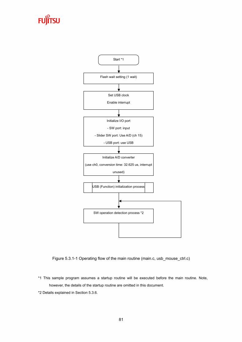
5.3.4 EP0 data receive process
The figure below shows the details for the EP0 data receive process.
Figure 5.3.4-1 EP0 data receive process (usb_mouse_ctrl.c)
EP0 data receive process
Get length of received data bytes
Get received data
(read from EP0DT register)
Clear DRQ0 flag
End

86
5.3.5 Setup command receive process
The figure below shows the details for the EP0 Setup command receive process. The
Setup command receive process also handles responses for the received Setup command.
Figure 5.4.5-1 Setup command receive process 1 (usb_mouse_ctrl.c)
Setup command receive process
Get received data byte length
Get receive data
(read from EP0DT register)
Clear SETP flag
Clear DRQ0 flag
No
SET IDLE received?
Clear DRQI flag
Yes
① ②

87
Figure 5.3.5-2 Setup command receive processing 2 (usb_mouse_ctrl.c)
①
No
Clear DRQI flag
Yes GET DESCRIPTOR (device)
received? Return Device Descriptor
(write to EP1DT register)
No
Clear DRQI flag
Yes GET DESCRIPTOR (config)
received? Return Configuration Descriptor
(write to EP1DT register)
No
Clear DRQI flag
Yes GET DESCRIPTOR (report)
received? Return Report Descriptor
(write to EP1DT register)
End
②

88
5.3.6 Switch operation detection process
The figures below show the details of the switch (pushbuttons and slider) operation
detection process. The device issues an HID data notification to the PC when it detects
switch operation. The sample program ignores simultaneous operation of multiple switches.
Figure 5.3.6-1 Switch operation detection process 1 (main.c)
Start
Get SW input status
SW4 (up) input?
Update mouse travel (X=5, Y=0)
SW6 (down) input?
Update mouse travel (X=-5, Y=0)
SW5 (right) input?
Update mouse travel (X=0, Y=-5)
SW3 (left) input?
Update mouse travel (X=0, Y=5)
①
Yes
Yes
Yes
Yes
No
No
No
No
Clear mouse travel (X=0, Y=0)

89
Figure 5.3.6-2 Switch operation detection process 2 (main.c)
No
①
Update click information (Bottom = 01h)
Yes
No
Yes
②
Update click information (Bottom = 02h) Update click information (Bottom = 00h)
SW9 (left click) input?
SW10 (left click) input?

90
Figure 5.3.6-3 Switch operation detection process 3 (main.c)
End
HID data notification process
②
No Update scroll data (wheel = 50)
Yes ad_data > ad_data_old?
No Update scroll data (wheel = -50)
Yes ad_data > ad_data_old?
Update scroll data (wheel = 0)
A/D conversion start (AD-ch15)
Yes
No
Get A/D conversion value
(ad_data=(A/D conversion value & 0x03E0) >> 23)
ad_data_old = ad_data
ad_data_old = ad_data
A/D conversion complete?

91
5.3.7 HID data notification process
The figure below shows the details of the HID data notification process.
Figure 5.3.7-1 HID data notification process (usb_mouse_ctrl.c)
Start
IN requested to EP1? DRQ=1?
End
No
No
Yes
Yes
Write HID data to be notified to PC (Host) in the
EP1DT register (button information, X/Y travel,
wheel movement)
Clear IN request flag to EP1 (DRQ=0)
HID data updates? No
Yes
Configuration completed?

92
6 Humidity sensor
6.1 What is humidity?
In the winter, our hands and skin tend to dry, and our throats easily become sore. Conversely, in areas where rain season occurs, the humidity tends to cause discomfort. And those who hang dry their laundry no doubt pay attention to the humidity level in weather reports.
Humidity represents the ratio of moisture in the air. The history of hygrometers used
to measure humidity is said to have started with the hair hygrometer, which utilizes the elasticity of hair. Today, in addition to hair hygrometers, inexpensive wet and dry bulb hygrometers are available and used in common households.
Humidity is often referred to in units of "relative humidity" (units: %RH), which is
defined as the ratio of water vapor pressure in air at a prescribed temperature, to the saturated vapor pressure at the same temperature, expressed as a percentage. Weather forecasts usually mention "percentage" alone, but the abbreviation for relative humidity is implied.
Other units used to refer to humidity include, wet-bulb temperature (units: °C), dew point temperature (units: °C), and water vapor content (units: ppmV for ratio by volume, and ppmW for volume by weight).
This text will express humidity in terms of relative humidity (%). 6.2 What is a humidity sensor?
The humidity sensor was developed as a replacement for the hygrometer. Humidity
sensors are used in air-conditioner temperature controls for offices and factories. Recent air conditioners for homes with dehumidifier and humidifier functions also make use of humidity sensors. Some microwave ovens use humidity sensors to control cooking temperature and time by detecting the amount of water vapor emitted from the heated food.
A humidity sensor uses the change in electrical properties caused by absorbing and
releasing moisture in the air. Because the sensor is constantly exposed to air, it is easily

93
affected by changes in its own materials caused by substances in the air, sometimes leading to performance loss. The material used in the sensor to detect humidity defines its type, such as high-molecular, metallic oxide, or electrolytic.
We will explain the most common type of humidity sensor, the high-molecular sensor.
The high-molecular film absorbs and releases moisture, thus creating a change in its permittivity which is used to measure the relative humidity in air.
One way of making this sensor is to place the high-molecular material between two electrodes, much like a capacitor. The permittivity change in the high-molecular film creates a measureable change in the capacitor's capacity. The electrodes are made of an extremely thin metal film that permits the passage of moisture as it is absorbed or released by the high-molecular film. A high-molecular humidity sensor can be of the capacity changing or resistance changing type. The explanation thus far is for a capacity changing type. The resistance changing type is made by affixing moisture sensitive material on a comb-like electrode and is simpler in construction than the capacity type. An added benefit of the resistance type is that it is not affected by the capacity of the wire leads, allowing wiring lengths to be as long as necessary.
Figure 8.2-1 Structure of a humidity sensor
Electrode
High-molecular
material
(moisture sensitive
material)
Electrode (comb-like)
Substrate Substrate
Capacity type Resistance type
High-molecular
material
(moisture sensitive
material)

94
The starter kit board has a humidity sensor device (HOKURIKU ELECTRIC
INDUSTRY CO., LTD) mounted to it. This is a resistance changing humidity sensor that uses a moisture sensitive polymer. This device must be driven by an alternating voltage as a constantly applied direct voltage can affect the device's properties.
In the next Chapter, we will explain the hygrometer program and power driving method as well as some cautionary notes.

95
7 Let's make a hygrometer
This sample program will create a hygrometer using the AD converter and base timer (PPG) in
the microcontroller (MB91F662) installed on the starter kit, and the humidity sensor also mounted
on the starter kit.
7.1 Overview of the sample program
This sample program measures humidity using the AD converter and base timer (PPG) in
the microcontroller (MB91F662), and the humidity sensor mounted on the starter kit. The
measured result is displayed on the 7-SEG LED on the starter kit. Figure 9.1-1 shows the
operation and details of the sample program.

96
<Sample program target project>
sample_humidity.abs - “sample_humidity.prj” [Debug]
< Sample program execution procedures>
1. Connect the starter kit to the PC with the USB cable.
2. Run the humidity sensor sample program.
3. The humidity is displayed in the 7-SEG LED.
Part name Silk printing on
board
Description
Humidity sensor HUMIDITY Detects humidity.
7-segment LED 7-SEG LED Displays humidity.
Figure 9.1-1 Operation and details of the humidity sensor sample program
Humidity
readout
You can view how the humidity
changes by touching the sensor.

97
7.2 Details on the humidity sensor
7.2.1 Wiring the humidity sensor
The humidity sensor on the starter kit board is wired as shown below.
Figure 9.2.1-1 Schematics of humidity sensor
PPG0
output port
PPG1
output port
A/D9
input port
Humidity sensor
Resistor 47 kΩ (Rs)
MB91F662
3.3V(Vin)

98
7.2.2 Driving the humidity sensor
The humidity sensor must be driven as follows.
Figure 9.2.2-1 Driving the humidity sensor
PPG0 output waveform
PPG1 output waveform
1kHz (Duty:50%)
A/D conversion
A/D conversion timing (PPG2)
Start A/D on lead edge of PPG2
+3.3V
0V
+3.3V
0V
1/2 to 2/3 of the timing when PPG0 is high

99
(1) Based on a setting in the MB91F662, PPG0 will output a pulse waveform at 1 kHz, 50%
duty. PPG1 will output the phase-inverted waveform of PPG0.
This will produce an alternating current of ±3.3 volts at the equivalent of 1 kHz between
the output pins of PPG0 and PPG1.
(2) The leading edge of PPG2 will trigger the A/D conversion.
The lead edge of PPG2 occurs when PPG0 is in its high phase, and allows reading of
the A/D input waveform when it is stable and near peak. This timing is about 1/2 to 2/3
the way along the pulse width of PPG0.
7.2.3 Humidity sensor characteristics
The voltage dividing characteristics of the humidity sensor on the starter kit are shown
below.
Figure 9.2.3-1 Voltage dividing characteristics of the humidity sensor 1
Voltage dividing characteristic V is calculated as V = Vin x Rs / (Rs + RH) where Vi is the input
voltage, RH is the impedance characteristic of the humidity sensor device, and Rs is the voltage
dividing resistance.
In the above formula, input voltage Vin = 3.3V, and dividing resistance Rs = 47 kΩ.
Voltage dividing characteristics data
Relative humidity (%RH)
Voltage dividing characteristics (V))

100
This sample program is designed for a fixed temperature of 22°C.
The voltage dividing characteristics at 22°C is given below.
Table 9.2.3-2 Humidity sensor voltage dividing characteristics table 2
* The figures in bold are the values used in this sample program.
Contact HOKURIKU ELECTRIC INDUSTRY CO., LTD., for the characteristics at temperatures
other than 22°C.
<Contact>
Sales support division, Head office, HOKURIKU ELECTRIC INDUSTRY CO., LTD.
E-mail: info-sales@hdk.co.jp
Relative
humidity
(%RH)
Voltage
dividing
characteristics
(V)
Relative
humidity
(%RH)
Voltage
dividing
characteristics
(V)
Relative
humidity
(%RH)
Voltage
dividing
characteristics
(V)
Relative
humidity
(%RH)
Voltage
dividing
characteristics
(V)
90 3.17 70 2.80 50 1.47 30 0.16
89 3.16 69 2.76 49 1.38 29 0.13
88 3.15 68 2.72 48 1.28 28 0.11
87 3.14 67 2.68 47 1.19 27 0.09
86 3.13 66 2.64 46 1.10 26 0.07
85 3.12 65 2.59 45 1.02 25 0.06
84 3.11 64 2.54 44 0.93 24 0.05
83 3.10 63 2.49 43 0.85 23 0.04
82 3.08 62 2.44 42 0.77 22 0.03
81 3.06 61 2.38 41 0.70 21 0.02
80 3.05 60 2.32 40 0.62 20 0.02
79 3.03 59 2.55 39 0.56 19
78 3.01 58 2.18 38 0.50 18
77 2.99 57 2.10 37 0.44 17
76 2.97 56 2.02 36 0.39 16
75 2.95 55 1.94 35 0.34 15
74 2.92 54 1.85 34 0.30 14
73 2.89 53 1.76 33 0.26 13
72 2.86 52 1.66 32 0.22 12
71 2.83 51 1.57 31 0.19 11
101
7.3 Sample program operating details
This section describes the operating details of the sample program.
7.3.1 Main routine
The operating conditions (setting conditions) for the peripheral functions of the MB91F662
used in this sample program are outlined below. The figure below shows the details of the
main routine.
<MB91F662 setting conditions>
FLASH access settings
FLASH access size setting: 32 bits (no changes to default value)
FLASH wait setting: 1 wait
MCU clock setting (set in the monitor debugger/no setting necessary)
CLKB (CPU): 32 MHz (External clock 4 MHz x PLL-8 multiplier setting)
CLKP (peripheral): 32 MHz (External clock 4 MHz x PLL-8 multiplier setting)

102
Figure 9.3-1 shows the flow of the main routine. This sample program measures time using the
interrupt of reload timer ch0. Processing for humidity calculation and LED display alternate every
two seconds so that changes can be observed in the LED display.
Figure 9.3.1-1 Operating flow of main routine
* This sample program assumes a startup routine will be executed before the main routine. Note, the
details of the startup routine are omitted in this document.
Start
Set Flash wait
- Initialize PPG ch0, ch1, ch2
(enable interrupt for PPG ch2)
- Initialize A/D converter
(enable interrupt, use FIFO)
- Initialize reload timer ch 0 (enable interrupt)
Calculate humidity
Enable interrupt
Enable operation of PPG ch0, ch1
2 sec elapsed?
Yes
No
7-SEG LED display process
Adjust PPG ch2 timing
Enable operation of PPG ch2

103
7.3.2 A/D converter interrupt processing
When 10 converted data values are written to the FIFO buffer, an A/D interrupt is
generated so that interrupt processing can take place. The interrupt processing routine
fetches 10 A/D conversions from the FIFO buffer, and averages them. This is treated as the
acquired value (value used to determine humidity) from the humidity sensor. The figure
below shows the details of the A/D converter interrupt processing routine.
Figure 9.3.2-1 A/D converter interrupt processing
A/D converter interrupt processing
- Stop A/D converter
- Clear interrupt causing bit
Get 10 A/D conversion results from FIFO
Calculate average (ad_average) from A/D
conversion results
Clear FIFO
End

104
7.3.3 Humidity calculation process
The figure below shows the details of the humidity calculation process. The voltage divisor
is obtained by multiplying the A/D conversion average by 0.00322 (= 3.3 volts / 210), because
the A/D converter has 10 bits of resolution. The humidity is found by looking up the voltage
divisor in Table 9.2.3-2, Humidity sensor voltage dividing characteristics table 2
Figure 9.3.3-1 Hygrometer calculation process
Humidity calculation process
End
Calculate voltage divisor.
( = ad_average x 0.00322)
Obtain humidity by looking up the voltage divisor in the
humidity sensor voltage division characteristics table.
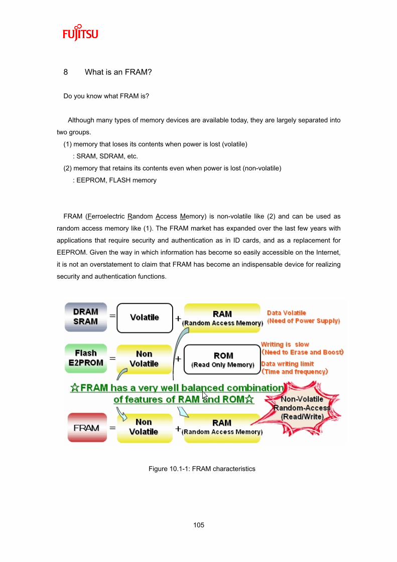
105
8 What is an FRAM?
Do you know what FRAM is?
Although many types of memory devices are available today, they are largely separated into
two groups.
(1) memory that loses its contents when power is lost (volatile)
: SRAM, SDRAM, etc.
(2) memory that retains its contents even when power is lost (non-volatile)
: EEPROM, FLASH memory
FRAM (Ferroelectric Random Access Memory) is non-volatile like (2) and can be used as
random access memory like (1). The FRAM market has expanded over the last few years with
applications that require security and authentication as in ID cards, and as a replacement for
EEPROM. Given the way in which information has become so easily accessible on the Internet,
it is not an overstatement to claim that FRAM has become an indispensable device for realizing
security and authentication functions.
Figure 10.1-1: FRAM characteristics

106
The characteristics of the FRAM are the very reason they are ideal for security-dependant
applications such as those in the figure below (train and bus passes, electronic money,
membership cards used to record profiles and preferences in addition to member information,
etc.). The following are typical examples.
- Unlike FLASH/EEPROM memory, FRAM does not require special command sequences such
as used for deleting data
(Data can be read and written just like RAM by specifying an address.
Data can be overwritten in units of bytes.)
- FRAM provides improved tamper-proofing of electronic key data for authentication
(Compared to FLASH and EEPROM, data on FRAM is difficult to read even when subject to
physical analysis)
- Authentication key data can be updated frequently and randomly.
- Requires less writing time after the FRAM power is switched from ON to OFF.
(The high-speed writing capability of the FRAM allows writing immediately after the power is
turned ON/OFF)
Figure 10.1-2. IC card applications such as electronic money

107
To learn more about FRAM,
Visit the Fujitsu website listed below.
http://jp.fujitsu.com/microelectronics/
The starter board is equipped with a stand-alone FRAM MB85RS256.
In the next Chapter, we will explain a program that accesses the FRAM using microcontroller
communications.

108
9 Let's make a counter
This sample program explains how to make a simple counter using FRAM. The counter
functionality is achieved by using the SPI communications function on the multifunction serial
interface (MFS), on the microcontroller (MB91F662) on this starter kit, to access the stand-alone
FRAM MB85RS256 (256 kbit).
9.1 Overview of the sample program
This sample program creates a counter using the FRAM and the functions of the serial
interface on the MB91F662. The FRAM is used to store counter data, while the pushbutton
switches are used to increment and clear the count, and toggle the 7-SEG LED display ON or
OFF.
Because the count is stored in FRAM, even if the power is turned off during operation by
disconnecting the USB cable, the counter will resume counting, when power is restored, exactly
from where it left off before losing power.
Figure 11.1-1 shows the operation and details of the sample program.

109
<Sample program target project>
sample_FRAM_SPI.abs - “sample_FRAM_SPI.prj” [Debug]
< Sample program execution procedures>
1. Connect the starter kit to the PC with the USB cable.
2. Run the FRAM sample program.
3. Pressing the pushbutton switch increments the count. (The count is retained even after
power is turned OFF.)
Increment data Toggles 7-SEG LED display
ON/OFF
For debug
Clear data
Counter readout

110
Part name Silk printing on
board
Description
FRAM FRAM Stores data.
Pushbutton SW P_SW7 Increments data by 1.
Pushbutton SW P_SW8 Clears data.
Pushbutton SW P_SW10 Toggles 7-SEG LED display ON/OFF.
LED Flashes while program is running.
7-segment LED 7-SEG LED Displays counter value.
Figure 11.1-1 Operation and details of the FRAM sample program

111
9.2 Details on the FRAM MB85RS256
The MB85RS256 is a stand-alone FRAM device with a 256-Kbit capacity that supports the SPI
interface. The features are listed below.
<Features>
- Bit configuration: 32,768 words x 8 bits
- Operating power supply voltage: 3.0 V to 3.6 V
- Operating frequency: 15 MHz (Max)
- Serial Peripheral Interface: SPI
- Operating temperature range: -20°C to 85°C
- Data retention: 10 years (+ 55°C)
- Read-write cycles: 1010 cycles/bit (min)
- Package: 8-pin plastic SOP (FPT-8P-M02)
<Connections>
Figure 11-2 shows a sample method of connection with the microcontroller (MCU).
Figure 11.2-1. FRAM connection with the microcontroller (MCU)
<OP-CODE>
The MB85RS256 accepts six commands specified in op-code. These commands are used to
access the FRAM. The commands are listed below.
Table 11.2-1 MB85RS256
Code name Description Op-code (Hex) (binary)
WREN Set Write Enable Latch 0x06 (0000110B)
WRDI Reset Write Enable Latch 0x04 (0000100B)
RDSR Read Status Register 0x05 (0000101B)
WRSR Write Status Register 0x01 (0000001B)
READ Read Memory Code 0x03 (0000011B)
WRITE Write Memory Code 0x02 (0000010B)
SCK
SI
SO
CS(GPIO)
HOLD(GPIO)
SCK
SI
SO
CS
HOLD
MCU
FRAM

112
The commands listed above are input to the FRAM synchronized with the clock (SCK) after
the trailing edge of the CS signal.
Reading is done by inputting the READ command followed by a 16-bit address. In response,
MB85RS256 outputs the 8-bit data synchronized with the clock. Thereafter, the address can be
incremented automatically to read 8 more bits of data repeatedly by inputting 8 clock pulses
before raising the CS signal.
Figure 11.2-2. Example of waveform when reading
CS
SCK
SI
SO
Clock (8 cycles)
Command 0x03 Address (16-bit)
Data (8-bit) Data (8-bit)
Address can be incremented automatically to
read another byte of data by inputting 8 cycles
of SCK before raising CS.

113
Writing is done by inputting the WRITE command followed by a 16-bit address, followed the
data to write in 8-bit units synchronized to the clock bit. Thereafter, the address can be
incremented automatically to continuously write 8 more bits of data by inputting data for every 8
clock pulses before raising the CS signal.
Before sending WRITE commands, writing must be enabled by issuing the WREN command.
Figure 11.2-3. Example of waveform when writing
CS
SCK
SI
SO
Clock (8 cycles)
Command 0x06 Address (16-bit)
Additional bytes of data can be written to the next
automatically incremented address by inputting 8 cycles of
SCK and 8 bits of data before raising CS.
Command 0x02 Data (8-bit)

114
9.3 Explanation of the sample program
This section explains the program for writing data to the FRAM using the SPI multifunction
serial interface on the MB91F662. Also refer to the actual sample program.
This sample program is only intended for a simple operation check and thus does not use the
multifunction serial interrupt function. The interrupt function including error processing should be
used when considering a system design.
This program was written based on the hardware connections shown in Figure 11.3-1.
Figure 11.3-1 Connections between the MB91F662 and MB85RS256
SCK9(P46):7pin
SIN9(P45):6pin
SOUT9(P44):5pin
P43:4pin
P47:8pin
P42:3pin
SCK
SI
SO
CS
HOLD
WP
MB91F662(MCU) FRAM MB85RS256

115
9.3.1 Main routine
The operation of the main routine is shown below. Note that the following conditions are
assumed when operating this sample program.
<MB91F662 setting conditions>
FLASH access settings
FLASH access size setting: 32 bits (no changes to default value)
FLASH wait setting: 1 wait
MCU clock setting (set in the monitor debugger/no setting necessary)
CLKB (CPU): 32 MHz (External clock 4 MHz x PLL-8 multiplier setting)
CLKP (peripheral): 32 MHz (External clock 4 MHz x PLL-8 multiplier setting)
Figures 11.3.1-1 to 11.3.1-3 show the flow of the sample program.
Figure 11.3.1-1 Counter operation flow (main.c Extint.c, sio.tx.c, fram_init.c)
Start
Initialize PORT (LED output)
Set Flash wait
Set CPU interrupt level
Enable interrupt
Initialize external interrupt
Initialize MFS (SPI mode)
Initialize FRAM (set control signals,
issue WRSR command)
Invert LED
Software loop
(wait for SW input)

116
Figure 11.3.1-2 Counter operation flow (Switch operation) (Extint.c, sio.tx.c)
Start interrupt routine
No
Yes
No
Yes
Read from FRAM address
0x0000
Set CPU interrupt level
(external interrupt level mask)
SW7 input?
Clear interrupt flag
LED_data < 99?
LED_data = LED_data +1
Issue WREN command to FRAM
Write LED_data to FRAM address
0x0000
LED_data = 0
Yes
SW8 input?
Clear interrupt flag
Issue WREN command to FRAM
Write 0x00 to FRAM address 0x0000
No
7-SEG LED output
Set CPU interrupt level
(enable external interrupt level)
End of interrupt routine
①
②

117
Figure 11.3.1-3 Counter operation flow (Extint.c, sio.tx.c)
①
No
Yes
No
Yes
SW10 input?
Clear interrupt flag
Lighting = 0 ?
Issue WREN command to FRAM
Write Lighting to FRAM address
0x0001
Lighting = 1
Lighting = 0
②

118
Appendix 1 Creating projects/sample programs as new projects
This Appendix will explain the settings to be made in order to create and debug new projects
and sample programs using the monitor debugger. The "Sample_skeleton" project file supplied
with the sample programs will be used for this explanation.
1.1 Sample project configuration
The "Sample_skeleton" folder is configured as shown below.
Figure 1 File organization in the sample project
Sample_skeleton
Debug
flash_erase_sec.bin
flash_write.bin
FshLdWrt.prc
main.c
Mon.h
sample_skeleton.dat
sample_skeleton.prj
start.prc
startup.asm
OPT*
sample_skeleton.sup
ABS
LST*
OBJ*
sample_skeleton.abs
sample_skeleton.mhx
sample_skeleton.bin
* Only files necessary for the explanation are shown here.
Files in the LST/OBJ/OPT folders have been omitted.

119
Launch SOFTUNE WORKBENCH, then from "File" - "Open Workspace" select sample.wsp in
the sample folder, or drag and drop the sample.wsp file onto the SOFTUNE workspace.
Clicking the + button next to "sample_skeleton.abs" will reveal the registered files as shown
below. Right-click on sample_skeleton.abs and select "Set as Active Project".
1.2 Explanation of the program
(1) startup.asm
This program contains code to set the stack pointer, define memory allocation, and initialize the
data area. (These parts of the code do not require changes and should be used as is.)

120
(2) main.c
The user program executes from the main () function.
Type your program from the line after the comment /* user program */.
Do not delete the code for internal FLASH memory access or the interrupt settings.
Set Flash wait
Set CPU interrupt servicing
level/ enable interrupt
User program goes here
Interrupt vector definitions for
monitor program

121
The monitor program is designed to allow communications with the PC at a peripheral clock
speed of 32 MHz.
Two header files are defined at the beginning of the program.
_fr.h defines the I/O registers for MB91F662.
(For details, refer to "ioregj.txt" in the sample program folder "IOH_MB91660_V01L02".)
mon.h is required to use the monitor program.
Interrupt vector definitions used by the monitor program are defined at the end of main.c. Do
not delete these definitions.
(3) FshLdWrt.prc / flash_write.bin / flash_erase_sec.bin
Files with the .prc extension are referred to as "procedure files (or batch files)".
These files can be invoked as "commands" while SOFTUNE is running.
FshLdWrt.prc is the command file for writing files created in SOFTUNE to the MB91F662
FLASH memory.
This file executes the flash_erase_sec.bin (FLASH sector erase command) and flash_write.bin
(FLASH write command) programs.
This file can be used without any modification for programs created using the
"sample_skeleton" project. (Note, the DATA_SIZE (*1) must be changed if the data size exceeds,
0x00004000.)
If you create a new workspace or project, the code indicated in italics (red) must be edited.
(All lines after the # are treated as comments.)
#-----------------------------------------------------------------------
set variable WRITE_SIZE = 0x00008000 # Data size to be written to FLASH
set variable DATA_SIZE = 0x00004000 #data size to initialize in FLASH (*1)
(Erases the sector that includes this range.)
set variable WRITE_ADR = 0x00080000 #Starting address in FLASH memory to write to
#Write data
set variable DATA_FILE = Debug¥ABS¥sample_skeleton.bin #Specify using relative path
(*2)
(- omitted -)
= load/debug Debug¥ABS¥sample_skeleton.abs #Specify using relative path (*2)
#-----------------------------------------------------------------------
(*1) Must be changed if the data size exceeds, 0x00004000.
(*2) Change to name of program you are creating.

122
(Project file name).abs will be generated after the make/build process.
The (project file name).bin file will be created from the mhx file using the converter program,
which in turn, will be created from the abs file. (This process will be described later)
This instruction in the FshLdWrt.prc file specifies the offset address of the user interrupt vector
area. Specify the same address as the starting address for the interrupt vector defined in main.c.
#-----------------------------------------------------
set register TBR = 0x00080000
#-----------------------------------------------------
1.3 SOFTUNE settings
This section explains the settings that must be made to use the monitor debugger on
SOFTUNE.
(1) Project settings
From the menu, select "Project" - "Project settings" to call up the project settings window. The
settings necessary for each tab will be explained.
(1)-1 "C/C++ compiler" tab
Select the "C/C++ compiler" tab and add the relative patch to the I/O register definition files in the
"Include path" category.

123
(1)-2 "Linker" tab
In the [Deployment/Link] category, press the "Section settings" button. The window shown in the
figure will appear. In "ROM/RAM area" select "_INROM01", and in section name specify "@INIT".
Then select "const" for the content type and press the "Set" button.
This area is where initial values for the variables with initial values (INIT area) will be located.

124
(1)-3 "Converter" tab
Place a check in the "Launch load module converter", and specify "Motorola S format (f2ms)"
as the conversion format. This setting will automatically generate an mhx file from the abs file
every time the make/build command is executed. (The mhx file is created inside the ABS folder.)
(2) Customize build settings
From the menu, select "Project" - "Customize build" to call up the window shown in the figure.

125
From the "Converter" folder in the tree view, select "After" and click the icon next to "New file".
Enter the name as shown below.
Title: M2BS (Any name may be specified)
Execution file name: C:¥Softune6¥Bin¥M2BS.EXE
Options: %X.mhx -o %X.bin -ran 0x00080000, 0x000FC000
Working directory: %x¥Debug¥ABS
After entering the above, click "OK" to save these settings.
These settings will convert the mhx file to a bin file. This file is written to the MB91F662 FLASH
memory using the FshLdWrt.prc file. (By registering this file in the customize build settings, the
bin file conversion is made each time the make/build command is executed.)
(3) Setup file
The setup file (extension sup) is located in the "Debug" folder of the SOFTUNE tree window. This
file must be configured before starting debugging.
Refer to Chapter 3, Section 3.2 for configuration instructions.

126
(4) Customize bar
After starting debugging on SOFTUNE, click "View" - "Customize bar" and specify "start.prc".
You can either type "start.prc" in the "Entry" box, or specify the file by clicking the button to the
right of the text box. Click "Add" to register the prc file to the corresponding number.
This will enable the customize bar icon for the registered number. Pressing the button will
execute the prc file.
Executing start.prc returns the PC to the starting address of the program.
(Note that this only returns the PC to the start address. It does not reset the devices.)

127
2 Verifying COM ports This Section will explain how to verify the COM ports allocated on your PC.
2.1 For Windows XP
Right-click "My Computer" and then select "Properties". In the "System properties" window,
select the "Hardware" tab and click the button "Device Manager".
In the device manager window, expand the "Ports (COM and LPT)" to see its contents.
Verify the number denoted by the ** in "USB Serial Port (COM**)".

128
In this example, the COM port is assigned
to "COM2".

129
3 Installation and usage of the PC writer
This starter kit is shipped with the monitor program written in the FLASH area of the
microcontroller. The monitor program must be running in order to connect to SOFTUNE, and to
use the continuous run and stop functions. If for some reason the monitor program fails to
operate correctly, the PC Writer must be used to rewrite it to the memory. We will use the PC
Writer to write the monitor program to the FLASH memory of the microcontroller.
The procedures for installing the PC writer are explained below.
Double-click "MB91F662_setup.exe" to launch the installer.
Click "Next".
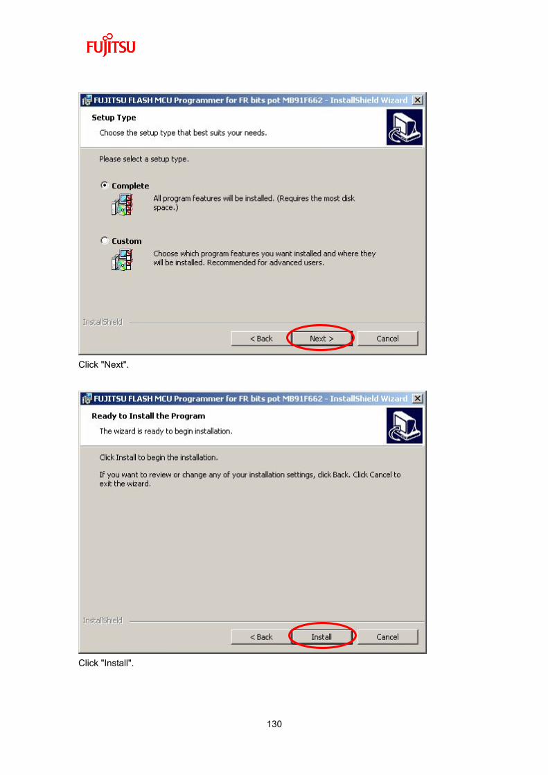
130
Click "Next".
Click "Install".

131
Wait for the installation to complete.
Click the "Finish" button to complete the installation of the PC writer.
After installing the PC writer, check the switch settings on the board before launching the
software.

132
(1) Set to "USB Mini-B".
(2) Set MODE0 to "PROG".
(3) MODE1 to "Debug".
(4) Set to "FUNC".
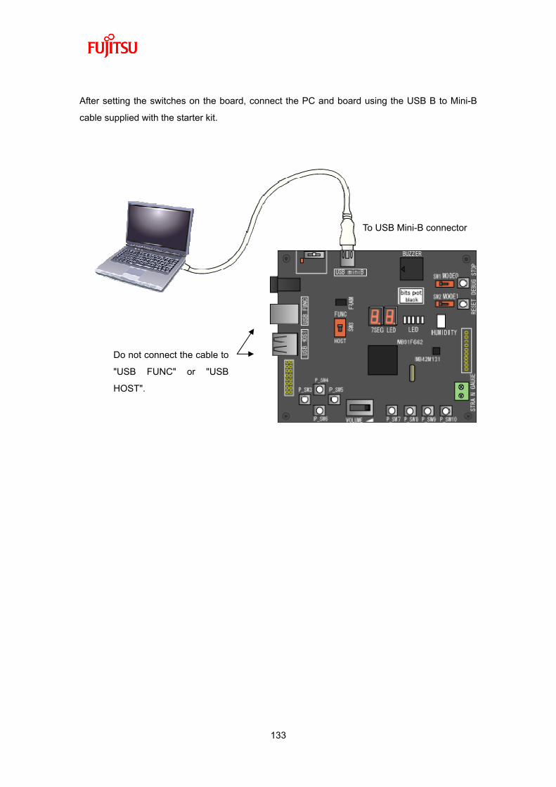
133
After setting the switches on the board, connect the PC and board using the USB B to Mini-B
cable supplied with the starter kit.
To USB Mini-B connector
Do not connect the cable to
"USB FUNC" or "USB
HOST".

134
After setting the switches on the board and connecting to the PC, launch PC Writer from the
Windows Start menu.
Click the "Set Environment" button and select the COM port being used. Refer to Appendix
12.1 to verify the COM port.
Select the COM port and click "OK" to close the Environment Settings window.
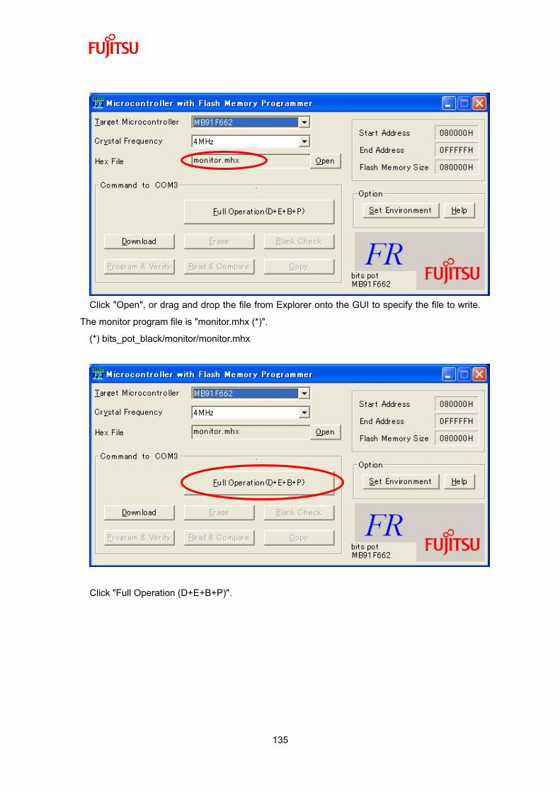
135
Click "Open", or drag and drop the file from Explorer onto the GUI to specify the file to write.
The monitor program file is "monitor.mhx (*)".
(*) bits_pot_black/monitor/monitor.mhx
Click "Full Operation (D+E+B+P)".

136
When the following window appears, press the reset button on the board, and then click OK on
the screen.
To USB Mini-B connector
Do not connect the cable to
"USB FUNC" or "USB
HOST".
After pressing the reset
button on the board, click
"OK" on the PC application.

137
Wait for the monitor program to finish writing to the microcontroller FLASH memory.
Writing to FLASH is complete when the message "Full Operation OK!" appears.
Click "OK" to close the window.

138
4 Monitor debugger
4.1 Explanation of the monitor debugger
Microcontrollers are usually made available as an evaluation device for program development
and test evaluation (debugging), and as a production device. The evaluation device connects to
the PC via an ICE (in-circuit emulator) that allows program development and debugging using
SOFTUNE on the PC. The ICE and evaluation device are equipped with debug-specific
functions.
On the other hand, the monitor debugger allows program development and debugging on the
production device. Monitor debugger is equipped with a minimum set of functions for debugging.
The user may use other additional functions for debugging as well. Although the monitor
debugger has limited functionality compared to debugging with an ICE, it is sufficient for program
development and debugging of small programs. The monitor debugger also allows program
development and debugging without the dedicated ICE hardware.

139
4.2 Resources used by monitor debugger
The resources used by the monitor debugger on this starter kit are listed in the following Table.
Resource Condition Remarks
RAM Approximately 8 Kbytes
0x3E000 to 0x3FFFF
FlashROM Approximately 8 Kbytes
0xFE000 to 0xFFFFF
Monitor vector table is placed at
0xFFC00 to 0xFFFFF
Multifunction
serial I/F
ch0
Wild register 0 to 16 ch Software break function
Reload timer ch2 Time measurement function
External interrupts:
ch30 (INT30) *
Forced break function I/O port
General-purpose I/O port: P63 Auto-boot function
INT9
(INTE command element)
Defines software break handler *1
(dbg_h)
INT12
(Step trace trap element)
Defines the step trace trap handler *2
(str_h)
Interrupt
External interrupt number for
forced break
Defines forced break handler *3 (abt_h)
Not necessary if not implementing the
force break function
* External interrupt: External interrupt channels 24 to 29, and 31 (INT24 to 29, 31) that share
the interrupt vector for ch30 (INT30) cannot be used as interrupts.

140
4.3 Memory map with monitor debugger installed
The figure below shows the memory map when the monitor debugger is installed on this starter
kit.
Built-in RAM
(48Kbyte)
Built ‒in ROM
(512Kbyte)
MB91F662

141
4.4 Monitor debugger limitations
The monitor debugger provided on this starter kit is functionally limited compared to an ICE as
listed below.
- "Program stop", "Reset" must be done by pressing the switch on the board.
(This cannot be controlled from SOFTUNE on the PC.)
- The operating clock for the CPU must not be changed as the monitor debugger program
performs data communications internally with the PC using asynchronous communications.
(This does not apply when checking the operation of a completed program.)
- The resources used by the monitor debugger cannot be used by the user.
(Refer to Appendix 4.2 for resources used by the monitor debugger.)
- Monitor debugger uses the following memory area. User programs cannot use this area.
RAM: 0x3E000 to 0x3FFFF, ROM: 0xFE000 to 0xFFFFF
(Refer to Appendix 4.3 for the memory map when the monitor debugger is installed.)
- Default interrupt vector area (TBR: 0xFFC00) is used by the monitor debugger. This area
cannot be overwritten when loading the monitor debugger. Therefore, the TBR is set to
0x80000 when monitor debugger launches.
- Only 16 break points (code breaks) are allowed.
- Monitor debugger uses user interrupts for the break function, communication functions, etc.
To use these interrupts in the user program, the interrupt vector addresses must be defined
outside of the monitor debugger.
Changing interrupt levels and enabling/disabling settings for interrupts in the user program
may disable certain monitor debugger functions.
- Do not press the Reset button on the board when launching the debugger.
- Do not press the Reset button on the board during continuous execution.

142
4.5 Stand-alone operation of the sample program
The starter kit can run sample programs without launching the debugger.
To run a program stand-alone, follow these procedures.
1. Make sure the program operates normally using monitor debugger.
2. Stop the monitor debugger
3. Change the microcontroller operation mode switch settings on the board from debug mode
to stand-alone mode. (See figure below)
4. Supply power to the board and press the Reset button to run the program.
(This example shows the connection for supplying USB bus power via the USB Mini-B cable.)
Figure Settings to run programs stand-alone
MODE0: RUN
MODE1: Stand-alone