FR-A700 PLC FUNCTION PROGRAMMING MANUALdownloadcentre.net/pdf_downloads/mitsubishi/A700 PLC...
183
INVERTER FR-A700 FR-A INVERTER PLC FUNCTION PROGRAMMING MANUAL PLC FUNCTION Chapter 1 CC-Link COMMUNICATION Chapter 2 SEQUENCE PROGRAMMING Chapter 3 ERROR CODE LIST Chapter 4 PLC FUNCTION PROGRAMMING MANUAL
Transcript of FR-A700 PLC FUNCTION PROGRAMMING MANUALdownloadcentre.net/pdf_downloads/mitsubishi/A700 PLC...
INVERTERFR-A700
HEAD OFFICE:MITSUBISHI DENKI BLDG MARUNOUCHI TOKYO 100-8310
FR-A
700INVERTER
PLC FU
NC
TION
PRO
GR
AM
MIN
G M
AN
UA
L
A
PLC FUNCTION Chapter 1
CC-Link COMMUNICATION Chapter 2
SEQUENCE PROGRAMMING Chapter 3
ERROR CODE LIST Chapter 4
PLC FUNCTIONPROGRAMMING MANUAL
IB(NA)-0600262EG-A(0509)MEE Printed in Japan Specifications subject to change without notice.

CO
NTE
NTS
I
CONTENTS
1. PLC FUNCTION 1
1.1 Function Block Diagram ...........................................................21.2 PLC Function Specifications....................................................31.3 System Configuration ...............................................................41.4 Wiring of the Inverter and Personal Computer Using
GX Developer for RS-485 Communication..............................51.5 Prior to Sequence Program Creation ......................................6
1.5.1 Precautions for sequence program creation ................................................. 61.5.2 Usable main GX Developer functions ........................................................... 61.5.3 Sequence program execution key................................................................. 71.5.4 Sequence program write ............................................................................... 81.5.5 Setting list of built-in PLC function parameter ............................................... 9
1.6 Device Map...............................................................................101.6.1 I/O device map ............................................................................................ 101.6.2 Internal relay (M) device map...................................................................... 121.6.3 Data register (D) device map ...................................................................... 121.6.4 Special relays.............................................................................................. 121.6.5 Special registers.......................................................................................... 14
1.7 Inverter Status Monitoring, Special Registers for Control ..201.7.1 Data that can be read at all times................................................................ 201.7.2 Data that are read by controlling (OFF to ON) the read command ............. 231.7.3 How to write data by controlling (OFF to ON) the write
command.................................................................................................... 251.7.4 Inverter operation status control.................................................................. 311.7.5 Inverter parameter access error (D9150) .................................................... 331.7.6 Inverter status (D9151)................................................................................ 33
1.8 Inverter Parameter Read/Write Method .................................341.8.1 Reading the inverter parameters................................................................. 341.8.2 Writing the inverter parameters ................................................................... 36
1.9 User Area Read/Write Method................................................381.9.1 User parameter read/write method.............................................................. 38
1.10 Analog I/O function .................................................................391.10.1 Analog input ................................................................................................ 391.10.2 Analog output .............................................................................................. 39
1.11 Paluse train input function .....................................................401.12 PID control ...............................................................................411.13 Inverter Operation Lock Mode Setting ..................................43

II
2. CC-Link COMMUNICATION 45
2.1 System Configuration.............................................................462.1.1 System configuration example.................................................................... 462.1.2 Function block diagram............................................................................... 47
2.2 CC-Link Parameters................................................................ 492.2.1 CC-Link Extended Setting (Pr. 544)............................................................ 49
2.3 CC-Link I/O Specifications ..................................................... 502.4 Buffer Memory......................................................................... 57
2.4.1 Remote output signals(Master module to inverter(FR-A7NC))....................................................... 57
2.4.2 Remote input signals Pr.544=100(Inverter(FR-A7NC) to master module)....................................................... 58
2.4.3 Remote registers Pr.544=100(Master module to inverter(FR-A7NC))....................................................... 59
2.4.4 Remote registers Pr.544=100 (Inverter(FR-A7NC) to master module)...................................................... 60
3. SEQUENCE PROGRAMMING 61
3.1 Overview ..................................................................................623.1.1 Outline of Operation Processings ............................................................... 62
3.2 RUN and STOP Operation Processings................................643.3 Program Makeup.....................................................................643.4 Programming Languages....................................................... 65
3.4.1 Relay symbolic language (Ladder mode) ................................................... 653.4.2 Logic symbolic language (List mode).......................................................... 67
3.5 Operation Processing Method of PLC Function ..................683.6 I/O Processing Method ...........................................................69
3.6.1 What is refresh system? ............................................................................. 693.6.2 Response delay in refresh system.............................................................. 70
3.7 Scan Time ................................................................................713.8 Numerical Values Usable in Sequence Program .................72
3.8.1 BIN (Binary Code)....................................................................................... 733.8.2 HEX (HEX Decimal).................................................................................... 74
3.9 Description of devices............................................................753.9.1 Device List .................................................................................................. 753.9.2 Inputs, Outputs X, Y.................................................................................... 763.9.3 Internal Relays M ........................................................................................ 793.9.4 Timers T...................................................................................................... 80

CO
NTE
NTS
III
3.9.5 100ms, 10ms and 100ms retentive timers .................................................. 803.9.6 Timer processing method and accuracy ..................................................... 81
3.10 Counters C ...............................................................................833.10.1 Count processing in refresh system............................................................ 843.10.2 Maximum counting speed of counter .......................................................... 85
3.11 Data Registers D......................................................................863.12 Special Relays, Special Registers .........................................873.13 Function List ............................................................................893.14 How to RUN/STOP the Built-in PLC Function from Outside (Re-
mote RUN/STOP) .....................................................................903.15 Watchdog Timer (Operation clog up monitor timer) ............923.16 Self-diagnostic Function ........................................................93
3.16.1 Error-time operation mode .......................................................................... 943.17 Keyword Registration .............................................................953.18 Setting of Output (Y) Status at Switching from STOP Status to
RUN Status...............................................................................963.19 Instruction Format...................................................................973.20 Bit Device Processing Method...............................................99
3.20.1 1-bit processing ........................................................................................... 993.20.2 Digit designation processing ....................................................................... 99
3.21 Handling of Numerical Value................................................1013.22 Operation Error......................................................................1023.23 Instructions List ....................................................................103
3.23.1 How to use the instruction list.................................................................... 1033.23.2 Sequence instruction................................................................................. 1053.23.3 Basic instructions ...................................................................................... 1073.23.4 Application instructions.............................................................................. 109
3.24 Description of the Instructions ............................................1103.25 Sequence Instructions..........................................................111
3.25.1 Contact Instructions : Operation start, series connection, parallel connection ... LD, LDI, AND, ANI, OR, ORI..................................................................................................... 111
3.25.2 Contact Instructions : Ladder block series connection, parallel connection ... ANB, ORB ................................................................................................. 113
3.25.3 Connection Instructions : Ladder block series connection, parallel connection ... ANB, ORB........... 117
3.25.4 Connection Instructions : Operation result, push, read, pop ... MPS, MRD, MPP............................. 120
3.25.5 Output Instructions : Bit device, timer, counter ... OUT............................. 123
IV
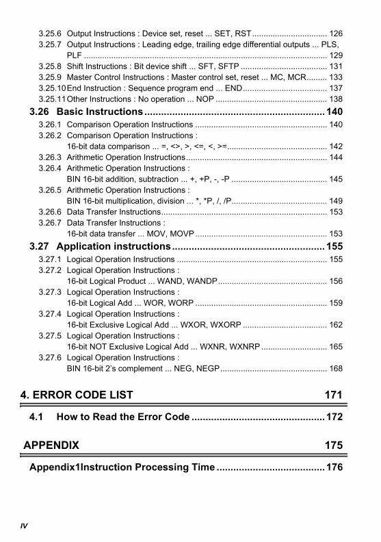
3.25.6 Output Instructions : Device set, reset ... SET, RST................................. 1263.25.7 Output Instructions : Leading edge, trailing edge differential outputs ... PLS,
PLF ........................................................................................................... 1293.25.8 Shift Instructions : Bit device shift ... SFT, SFTP ...................................... 1313.25.9 Master Control Instructions : Master control set, reset ... MC, MCR......... 1333.25.10End Instruction : Sequence program end ... END..................................... 1373.25.11Other Instructions : No operation ... NOP ................................................. 138
3.26 Basic Instructions................................................................. 1403.26.1 Comparison Operation Instructions .......................................................... 1403.26.2 Comparison Operation Instructions :
16-bit data comparison ... =, <>, >, <=, <, >=............................................ 1423.26.3 Arithmetic Operation Instructions.............................................................. 1443.26.4 Arithmetic Operation Instructions :
BIN 16-bit addition, subtraction ... +, +P, -, -P .......................................... 1453.26.5 Arithmetic Operation Instructions :
BIN 16-bit multiplication, division ... *, *P, /, /P.......................................... 1493.26.6 Data Transfer Instructions......................................................................... 1533.26.7 Data Transfer Instructions :
16-bit data transfer ... MOV, MOVP.......................................................... 1533.27 Application instructions....................................................... 155
3.27.1 Logical Operation Instructions .................................................................. 1553.27.2 Logical Operation Instructions :
16-bit Logical Product ... WAND, WANDP................................................ 1563.27.3 Logical Operation Instructions :
16-bit Logical Add ... WOR, WORP .......................................................... 1593.27.4 Logical Operation Instructions :
16-bit Exclusive Logical Add ... WXOR, WXORP ..................................... 1623.27.5 Logical Operation Instructions :
16-bit NOT Exclusive Logical Add ... WXNR, WXNRP ............................. 1653.27.6 Logical Operation Instructions :
BIN 16-bit 2’s complement ... NEG, NEGP............................................... 168
4. ERROR CODE LIST 171
4.1 How to Read the Error Code ................................................ 172
APPENDIX 175
Appendix1Instruction Processing Time ....................................... 176

1. PLC FUNCTION
1
Chapter 1
Chapter 2
Chapter 3
Chapter 4
This manual describes the functions and devices necessary for programming.
1.1 Function Block Diagram ...................................... 21.2 PLC Function Specifications............................... 31.3 System Configuration .......................................... 41.4 Wiring of the Inverter and Personal Computer
Using GX Developer for RS-485 Communication... 51.5 Prior to Sequence Program Creation ................. 61.6 Device Map............................................................ 101.7 Inverter Status Monitoring, Special Registers
for Control ............................................................. 201.8 Inverter Parameter Read/Write Method .............. 341.9 User Area Read/Write Method ............................. 381.10 Analog I/O function .............................................. 391.11 Paluse train input function .................................. 401.12 PID control ............................................................ 411.13 Inverter Operation Lock Mode Setting ............... 43

2
Function Block Diagram
1.1 Function Block DiagramHow I/O data are transferred to/from the inverter by the built-in PLC function isexplained using function blocks.(1) I/O data read, write, etc. can be performed by accessing the inverter in the
predetermined method using special relays, special registers, etc.(2) Operation, parameter read/write, etc. can be performed in accordance with the
created sequence programs (built in the inverter) using input data from the controlinput terminals.With the output signals, output data can be output to outside the inverter from thecontrol output terminals as not only the inverter's status signals but also pilot lampon/off, interlock and other control signals set freely by the user.
Input signal
Inverter
Output signal
I/O data
Special relays, special registers,etc.
Built
-in s
eque
nce
prog
ram
Inve
rter C
PU

3
PLC Function Specifications
1
PLC
FU
NC
TIO
N
1.2 PLC Function SpecificationsThe following table indicates the program capacity and devices of the PLC function.
*1 These signals use the same terminals as used by the input and output signals given in thecommon specifications of the inverter.One point is always necessary for a sequence start (RUN/STOP).
*2 As inverter control is also performed actually, the scan time is approximately 40ms at 500 steps.
A700 Sequence SectionControl method Repeated operation (by stored program)I/O control method Refresh
Programming language Relay symbolic language (ladder mode)Logic symbolic language (list mode)
Num
ber o
f in
stru
ctio
n PLC instructions 23Basic instructions 32
Application instructions 18
Processing speed PLC instruction 1.9µs to 12µs/step(*2)
Number of I/O points
128 (X: 64 points, Y: 64 points) 19 points installed, X: 12 points, Y: 7 points (*1)FR-A7AX, X: 16 pointsFR-A7AY, Y: 6 pointsFR-A7AR, Y: 3 points
Number of analog I/O points 5 points installed, Input: 3 points, Output: 2 pointsFR-A7AY output: 2 points
Watchdog timer 10 to 2000(ms)Memory capacity 6k bytes used by sequence and parameters.Program capacity 1k step
Dev
ices
Internal relay (M) 64(M0 to M63)Latch relay (L) None (Can be set with parameters but will not latch)Step relay (S) None (Can be set with parameters but will operate as M)Link relay (B) None
Timer (T)Points 16
Specifications100ms timer: Set time 0.1 to 3276.7s (T0 to T15)10ms timer: Set time 0.01 to 327.67s100ms retentive timer: Set time 0.1 to 3276.7s
Counter (C)Points 16
Specifications Normal counter: Setting range 1 to 32767 (C0 to C15)Interrupt program counter: None
Data device (D) 120(D0 to D119)Link register (W) NoneAnnunciator (F) NoneFile register (R) NoneAccumulator (A) NoneIndex register (Z, V) NonePointer (P) NoneInterrupt pointer (I) NoneSpecial relay (M) 256 (M9000 to 9255) with function limitSpecial register (D) 256 (D9000 to 9255) with function limit

4
System Configuration
1.3 System ConfigurationThe following shows the system configuration for use of the PLC function.<System configuration example>
Communication specificationsSet the following setting in communication parameters of the inverter.
Inverter Parameter GX Developer Setting Inverter initial settingPr.118 PU communication speed 96 (9600bps) 192 (19200bps)
Pr.119 PU communication stop bit length 0 (data length: 8 bits, stop bit: 1 bit)
1 (data length: 8 bits, stop bit: 2 bit)
Pr.120 PU communication parity check 1 (with odd parity check) 2 (with even parity check)Pr.122 PU communication check time interval
9999 (without communication check)
9999 (without communication check)
REMARKS•For futher details, refer to the Inverter instruction manual (applied).
POINT•Support GX Developer ver.8.0 or more•GX Developer Setting
REMARKS•Refer to the Inverter instruction manual (applied) for wiring.•Refer to the GX Developer manuals for the specifications related to GX Developer and thepersonal computer that uses GX Developer.GX Developer Version xx Operating manualGX Developer Version xx Operating manual (startup)
•The programming tool that can be used is GX Developer only. (The A6GPP, A7PHP, etc.cannot be used.)
3-phase AC power supply
FR-A700
RS-232C/RS-485converter
GX Developer:Programming tool
PU connector
Motor
PLC series ACPUPLC type A0J2H
[Project data list]→[Parameter]→[PLC parameter]→[A parameter]→«Memory capacity» tab→"Program capacity"→"Sequence"→"main" 1k step

5
Wiring of the Inverter and Personal Computer UsingGX Developer for RS-485 Communication
1
PLC
FU
NC
TIO
N
1.4 Wiring of the Inverter and Personal Computer UsingGX Developer for RS-485 Communication
Personal computer - inverter connection cable Make connection after conversion between RS-232C and RS-485.
Examples of commercially available products (as of Sep., '05)
Type MakerSC-FRPC BEIJERS
REMARKSWhen fabricating the cable on the user side, refer to the inverter instruction manual (applied).
PU connector
Personal computer
GX Developer :Programming tool
RS-232C connector
RS-232C-RS-485
converter

Prior to Sequence Program Creation
6
1.5 Prior to Sequence Program Creation
1.5.1 Precautions for sequence program creation
If any of the instructions (refer to page 103) and devices (refer to page 3) that cannotbe used with the built-in PLC function exists in a sequence program, an instructioncode error occurs at the execution of that instruction.Error code D9008=10Operation error step D9010
D9011
1.5.2 Usable main GX Developer functionsParameter or sequence program read/writeLadder monitorDevice monitorDevice testAll device memory clearRemote RUN/STOP
POINT•Online change of the sequence program and access to other stations are notallowed. In addition, program read/write from other stations and all PLC memory clearcannot be performed.
•Back up the ladder configured with the protective function of GX Developer.
REMARKS•Refer to page 22 for the error codes.
CAUTIONDevice test ([Online] - [Debug] - [Device test]) of GX Developer can be performed, but ifdevices corresponding to control terminal (e.g. STF, STR) signals are tested, thedevices turn on in the sequence but the inverter does not perform the correspondingoperation.

Prior to Sequence Program Creation
PLC
FU
NC
TIO
N
7
1
1.5.3 Sequence program execution keyThe sequence program execution key (STOP/RUN) of the PLC is switched by turningoff/on the SQ signal.
Open (STOP) the SQ signal-SD terminals when writing a sequence program, forexample.When executing the sequence program, short (RUN) the SQ signal-SD terminals.Remote run/stop of the built-in PLC function can be executed in any of the followingmethods:• Setting using the built-in PLC function parameter (contact)• Using GX Developer• Via CC-Link communication (refer to page 49)
POINT•For the terminal used for SQ signal input, set "50" in any of Pr.178 to Pr. 189 toassign the function.
•SQ-SD must be shorted to execute the built-in PLC function.
REMARKS•The validity limit of the SQ signal can be controlled using Pr.415 Inverter operation lock modesetting. (Refer to page 43.)
CAUTIONThe outputs (Y) are cleared by turning the SQ signal off (STOP) after sequence programexecution (SQ signal on).The other devices retain the device data prior to STOP. When you want to clear theremaining device data, power off or reset (short RES-SD for 0.1s, then open) theinverter.
CAUTIONIf the SQ signal is not turned on, the start signal of the inverter is designed tobecome valid by the factory setting of Pr.415 Inverter operation lock mode setting.
Prior to Sequence Program Creation
8
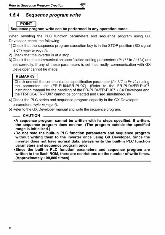
1.5.4 Sequence program write
When rewriting the PLC function parameters and sequence program using GXDeveloper, check the following:1)Check that the sequence program execution key is in the STOP position (SQ signal
is off) (refer to page 7).2)Check that the inverter is at a stop.3)Check that the communication specification setting parameters (Pr.117 to Pr.124) are
set correctly. If any of these parameters is set incorrectly, communication with GXDeveloper cannot be made.
4)Check the PLC series and sequence program capacity in the GX Developer parameters (refer to page 4).
5) Refer to the GX Developer manual and write the sequence program.
POINTSequence program write can be performed in any operation mode.
REMARKSCheck and set the communication specification parameter (Pr. 117 to Pr. 124) usingthe parameter unit (FR-PU04/FR-PU07). (Refer to the FR-PU04/FR-PU07instruction manual for the handling of the FR-PU04/FR-PU07.) GX Developer andthe FR-PU04/FR-PU07 cannot be connected and used simultaneously.
CAUTION•A sequence program cannot be written with its steps specified. If written,the sequence program does not run. (The program outside the specifiedrange is initialized.)
•Do not read the built-in PLC function parameters and sequence programwithout writing them to the inverter once using GX Developer. Since theinverter does not have normal data, always write the built-in PLC functionparameters and sequence program once.
•Since the built-in PLC function parameters and sequence program arewritten to the flash ROM, there are restrictions on the number of write times.(Approximately 100,000 times)

9
Function Block Diagram
1
PLC
FU
NC
TIO
N
1.5.5 Setting list of built-in PLC function parameterThe built-in PLC function parameters are designed to specify the ranges of using thePLC function, e.g. program capacity, device assignment and various functions.
Item GX Developer Default Setting Range<Usable device range>
Sequence program capacity 6k steps 1k step
File register capacity None Cannot be set (default)Comment capacity None Cannot be set (default)Status latch None Cannot be set (default)Sampling trace None Cannot be set (default)Microcomputer program capacity None Cannot be set (default)
Latch range setting L1000 to L2047 Cannot be set (invalid if set)Link range setting None Cannot be set (default)I/O assignment None Cannot be set (default)
Internal relay, latch relay, step relay setting
M0 to 999L1000 to 2047
None for S
L and S cannot be set.(Operates as M if set)<M0 to M63>
Watchdog timer setting 200ms 10 to 2000ms
Timer setting
100ms: T0 to 19910ms: T200 to 255
(100ms timers since only T0 to 7 are available)
16 points for 100ms, 10ms and retentive timers. Timers have consecutive numbers.<T0 to T15>
Counter setting Without interrupt counters Cannot be set (default)<C0 to C15>
Remote run/pause NoneCan be set using X0 to 1F. Otherwise invalid. Pause does not function.
Error-time operation mode
Fuse blow: Continued Setting invalid (since there are no fuses)
I/O verify error: Stop Setting invalid (since there are no I/O modules)
Operation error: Continued Stop/ContinuedSpecial function module check
error: StopSetting invalid (since there are no special modules)
STOP → RUN output mode Operation status prior to STOP is re-output.
Prior to STOP/after operation execution
Print title registration None Cannot be set
Keyword registration None Online setting cannot be made but parameter setting is valid.
REMARKS•The following functions are not supported.1. Constant scan, 2. Latch (device data backup for power failure), 3. Pause, 4. Status latch, 5. Sampling trace, 6. Offline switch
•If parameter clear of the inverter is performed, the above built-in PLC function parameters arenot cleared.
•For the built-in PLC function parameter setting operation, refer to the GX DeveloperOperating Manual.

Device Map
10
1.6 Device Map
1.6.1 I/O device mapDevice
No. Name Remarks Device No. Name Remarks
Ext
erna
l I/O
X00 STF terminal
External terminal
Y00 RUN terminal
External terminal
X01 STR terminal Y01 SU terminalX02 RH terminal Y02 OL terminalX03 RM terminal Y03 IPF terminalX04 RL terminal Y04 FU terminalX05 JOG terminal Y05 ABC1 terminalX06 RT terminal Y06 ABC2 terminalX07 AU terminal Y07
Empty
X08 CS terminal Y08X09 MRS terminal Y09X0A STOP terminal Y0AX0B RES terminal Y0BX0C
Empty
Y0CX0D Y0DX0E Y0EX0F Y0F
Plu
g in
opt
ion
I/O
X10 X0 terminal
16bit digital InputFR-A7AX
Y10 DO0 terminal
Dgital outputFR-A7AY
X11 X1 terminal Y11 DO1 terminalX12 X2 terminal Y12 DO2 terminalX13 X3 terminal Y13 DO3 terminalX14 X4 terminal Y14 DO4 terminalX15 X5 terminal Y15 DO5 terminalX16 X6 terminal Y16 DO6 terminalX17 X7 terminal Y17 RA1 terminal Relay
outputFR-A7AR
X18 X8 terminal Y18 RA2 terminalX19 X9 terminal Y19 RA3 terminalX1A X10 terminal Y1A
Empty
X1B X11 terminal Y1BX1C X12 terminal Y1CX1D X13 terminal Y1DX1E X14 terminal Y1EX1F X15 terminal Y1F
Device Map
PLC
FU
NC
TIO
ND
evic
e M
ap
11
1
Sys
tem
I/O
X20 Operation mode setting read completion D9140 Y20 Operation mode setting
read command D9140
X21 Set frequency read completion (RAM) D9141 Y21 Set frequency read
command (RAM) D9141
X22Set frequency read completion (E2PROM)
D9142 Y22Set frequency read command (E2PROM)
D9142
X23 Operation mode setting write completion D9143 Y23 Operation mode setting
write command D9143
X24 Set frequency write completion (RAM) D9144 Y24 Set frequency write
command (RAM) D9144
X25Set frequency write completion (E2PROM)
D9145 Y25Set frequency write command (E2PROM)
D9145
X26 Alarm definition batch clear completion D9146 Y26 Alarm definition batch
clear command D9146
X27 Parameter clear completion D9147 Y27 Parameter clear commandD9147
X28 Parameter read completion (RAM) D9241,
D9242,D9234
Y28 Parameter read request (RAM) D9241,
D9242,D9234X29 Parameter write
completion (RAM) Y29 Parameter write request (RAM)
X2A Parameter read completion (EEPROM) D9243,
D9244,D9235
Y2A Parameter read request (EEPROM) D9243,
D9244,D9235X2B Parameter write
completion (EEPROM) Y2B Parameter write request (EEPROM)
X2C
System area
Y2C
System areaX2D Y2DX2E Y2EX2F Y2F
CC
-Lin
k I/O
rem
ote
I/O
X30 RY0
FR-A7NC
Y30 RX0
FR-A7NC
X31 RY1 Y31 RX1X32 RY2 Y32 RX2X33 RY3 Y33 RX3X34 RY4 Y34 RX4X35 RY5 Y35 RX5X36 RY6 Y36 RX6X37 RY7 Y37 RX7X38 RY8 Y38 RX8X39 RY9 Y39 RX9X3A RYA Y3A RXAX3B RYB Y3B RXBX3C RYC Y3C RXCX3D RYD Y3D RXDX3E RYE Y3E RXEX3F RYF Y3F RXF
Device No. Name Remarks Device
No. Name Remarks

Device Map
12
1.6.2 Internal relay (M) device map
1.6.3 Data register (D) device map
1.6.4 Special relaysThe special relays are internal relays with special applications and therefore shouldnot be switched on-off in the program.
Device No. DescriptionM0 to M63 Use freely on user side.
Data Register (D)
Inverter Pr. Number Parameter Name Reference
PageD0 to D99 Use freely on user side. —
D100 to D119 Pr.506 to Pr.515 User parameters. Use freely on user side. 38
Number Name DescriptionM9008 Self-diagnostic error Turned on by self-diagnosed error.
M9010 Operation error flag Turned on by an instruction execution error.Turned off when error is removed.
M9011 Operation error flag Turned on by an instruction execution error.Remains on after normal status is restored.
M9036 Normally ONM9036 and M9037 are turned on and off independently of STOP or RUN.M9038 and M9039 change depending on the STOP or RUN status. In other than the STOP status, M9038 is on for one scan only and M9039 is off for one scan only.
M9037 Normally OFF
M9038 On only for 1 scan after RUN
M9039 Off only for 1 scan after RUN
M9200 Inverter operation status control flag (STF)
Control the STF terminal of the inverter from PLC function
M9201 Inverter operation status control flag (STR)
Control the STR terminal of the inverter from PLC function
M9202 Inverter operation status control flag (RH)
Control the RH terminal of the inverter from PLC function
M9203 Inverter operation status control flag (RM)
Control the RM terminal of the inverter from PLC function
M9204 Inverter operation status control flag (RL) Control the RL terminal of the inverter from PLC function
M9205 Inverter operation status control flag (JOG)
Control the JOG terminal of the inverter from PLC function
M9206 Inverter operation status control flag (RT) Control the RT terminal of the inverter from PLC function
M9207 Inverter operation status control flag (AU)
Control the AU terminal of the inverter from PLC function
M9208 Inverter operation status control flag (CS)
Control the CS terminal of the inverter from PLC function
M9209 Inverter operation status control flag (MRS)
Control the MRS terminal of the inverter from PLC function
M9210 Inverter operation status control flag (STOP)
Control the STOP terminal of the inverter from PLC function
Device Map
PLC
FU
NC
TIO
ND
evic
e M
ap
13
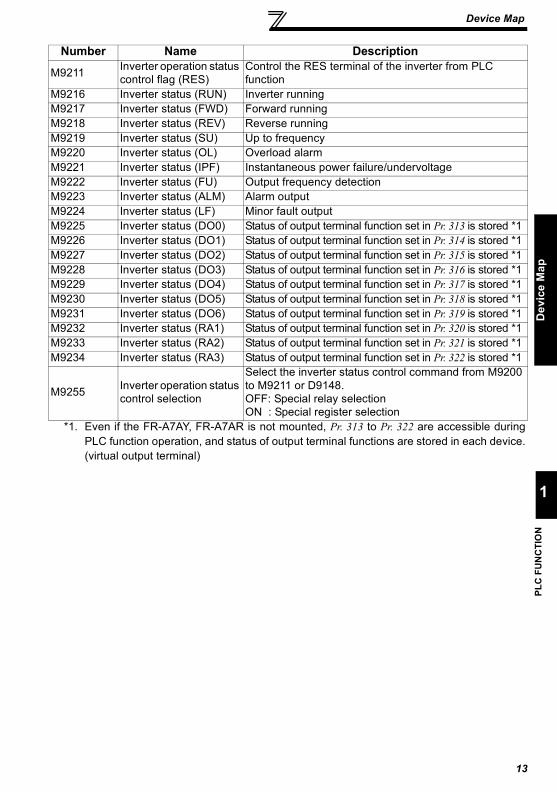
1
M9211 Inverter operation status control flag (RES)
Control the RES terminal of the inverter from PLC function
M9216 Inverter status (RUN) Inverter runningM9217 Inverter status (FWD) Forward runningM9218 Inverter status (REV) Reverse runningM9219 Inverter status (SU) Up to frequencyM9220 Inverter status (OL) Overload alarmM9221 Inverter status (IPF) Instantaneous power failure/undervoltageM9222 Inverter status (FU) Output frequency detectionM9223 Inverter status (ALM) Alarm outputM9224 Inverter status (LF) Minor fault outputM9225 Inverter status (DO0) Status of output terminal function set in Pr. 313 is stored *1M9226 Inverter status (DO1) Status of output terminal function set in Pr. 314 is stored *1M9227 Inverter status (DO2) Status of output terminal function set in Pr. 315 is stored *1M9228 Inverter status (DO3) Status of output terminal function set in Pr. 316 is stored *1M9229 Inverter status (DO4) Status of output terminal function set in Pr. 317 is stored *1M9230 Inverter status (DO5) Status of output terminal function set in Pr. 318 is stored *1M9231 Inverter status (DO6) Status of output terminal function set in Pr. 319 is stored *1M9232 Inverter status (RA1) Status of output terminal function set in Pr. 320 is stored *1M9233 Inverter status (RA2) Status of output terminal function set in Pr. 321 is stored *1M9234 Inverter status (RA3) Status of output terminal function set in Pr. 322 is stored *1
M9255 Inverter operation status control selection
Select the inverter status control command from M9200 to M9211 or D9148.OFF: Special relay selectionON : Special register selection
*1. Even if the FR-A7AY, FR-A7AR is not mounted, Pr. 313 to Pr. 322 are accessible duringPLC function operation, and status of output terminal functions are stored in each device.(virtual output terminal)
Number Name Description

Device Map
14
1.6.5 Special registersThe special registers are data registers with special applications and therefore datashould not be written to the special registers in the program.
Number Name Description Page
Spec
ial r
egis
ters
D9008 Self-diagnostic error
Stores the self-diagnosed error number in BIN. (Refer to page 22 for the error codes.) 22
D9010 Operation error step
Stores the step number in BIN, at which an instruction execution error occurred. After that, data is updated each time operation error occurs.
—
D9011 Operation error step
Stores the step number in BIN, at which an instruction error occurred. Since data is stored into D9011 when M9011 turns from off to on, D9011 data is not updated unless M9011 is cleared by the user program.
—
D9014 I/O control method 3 (fixed): Both input and output refreshes —
D9015 CPU operating status
Stores the operating status of the PLC function.
—
D9016 Program numberStores the number that indicates which sequenceprogram is currently in execution.1 (fixed): Main program (RAM)
—
D9017Minimum scan time(10ms units)
Stores the scan time at every END that is smaller than D9017 data, i.e. stores the minimum scan time in BIN. —
D9018 Scan time(10ms units)
Stores and updates the scan time at every END in BIN. —
D9019Maximum scan time(10ms units)
Stores the scan time at every END that is greater than D9019 data, i.e. stores the maximum scan time in BIN.
—
D9062 to D9093 Remote registers Special registers for communication with the master
station in CC-Link. 50
RUNSTOP
01
B15 B12B11 B8B7 B4B3 B0
RUNSTOP
01
RUNSTOP
01
Remote run/stopusing GX Developer
Remote run/stop usingsequence parameter setting
Shorting/opening SQ-SD
Invalid
Device Map
PLC
FU
NC
TIO
ND
evic
e M
ap
15
1
Spec
ial r
egis
ters
for c
ontro
l
D9133 Output frequency monitor
Stores the current output frequency.0.01Hz units
20D9134 Output current monitor
Stores the current output current.0.01A units
D9135 Output voltage monitor
Stores the current output voltage.0.1V units
D9136 Error history 1, 2Store the errors that occurred in the inverter in order of occurrence. 21
D9137 Error history 3, 4D9138 Error history 5, 6D9139 Error history 7, 8
D9140 Operation mode setting read Stores the current operation mode. 23
D9141 Set frequency read (RAM) Reads and stores the set frequency (RAM). 24
D9142Set frequency read (E2PROM)
Reads and stores the set frequency (EEPROM). 24
D9143 Operation mode setting write Sets a new operation mode. 26
D9144 Set frequency write (RAM) Sets the running frequency (RAM). 27
D9145Set frequency write (E2PROM)
Sets the running frequency (EEPROM). 28
D9146 Alarm definition batch clear Write H9696 to clear the error history. 29
D9147 Parameter clear
H9696 write: Parameter clearH9966 write: All clearH5A5A write:Parameter clear except communication
parametersH55AA write:All clear except communication
parametersDuring GX Developer communication, perform clearing by H5A5A or H55AA.
30
Number Name Description Page

Device Map
16
Spec
ial r
egis
ters
for c
ontro
l
D9148 Inverter operation status control
Turn on/off the corresponding bits to control the inverter operation status.The initial value: All "0". When M9255 is off, this device does not function.
31
D9149
Inverter operation status control enable/disable setting
Enable/disable the inverter operation status control using D9148 and M9200 to M9211 by turning on/off the corresponding bits.Bit image is the same as D9148.The initial value: All "0" (invalid)
32
D9150Inverter parameter access error
Stores the error No. when an error occurs because the data stored in the parameter or special register is not reflected on the inverter.
33
D9151 Inverter status
Stores the running status and operating status of the inverter.
33
D9152 Frequency setting 0.01Hz units —
D9153 Running speed 1(0.1)r/min unit —D9154 Motor torque 0.1% units —
D9155 Converter output voltage 0.1V units —
D9156 Regenerative brake duty 0.1% units —
D9157Electronic thermal relay function load factor
0.1% units —
D9158 Output current peak value 0.01A/0.1A units —
Number Name Description Page
B15 B12B11 B8B7 B4B3 B00:OFF1:ON
STFSTRRHRMRLJOGRTAUCSMRSSTOPRES
Invalid
B15 B8B7 B4B3 B00:OFF1:ON
Inverter running(RUN)Forward runningReverse runningUp to frequency(SU)Overload alarm(OL)Instantaneous power failure/undervoltage(IPF)Output frequency detection(FU)Alarm output(ALM)Minor fault output(LF)

Device Map
PLC
FU
NC
TIO
ND
evic
e M
ap
17
1
Spec
ial r
egis
ters
for c
ontro
l
D9159 Converter output voltage peak value 0.1V units —
D9160 Input power 0.01kW/0.1kW units —D9161 Output power 0.01kW/0.1kW units —
D9162 Input terminal status
Input terminal status details
—
D9163 Output terminal status
Output terminal status details
—
D9164 Load meter 0.1% units —
D9165 Motor excitation current 0.01A/0.1A units *7 —
D9166 Position pulse —
D9167 Cumulative energization time 1h units —
D9169 — Always 0 —
D9170 Actual operation time 1h unit —
D9171 Motor load factor 0.1% units —D9172 Cumulative power 1kW unit —D9179 Torque command 0.1% units —
D9180 Torque current command 0.1% units —
D9181 Motor output 0.01kW units —D9182 Feedback pulse 1 unit —
D9197 Power saving effect
Variable according to parameters—
D9198 Cumulative saving power —
D9199 PID set point 0.1% units —
D9200 PID measured value 0.1% units —
D9201 PID deviation 0.1% units —
Number Name Description Page
B15 B12B11 B8B7 B4B3 B00:OFF1:ON
STFSTRAURTRLRMRHJOGMRSSTOPRESCS
B15 B7 B4B3 B00:OFF1:ON
RUNSUIPFOLFUABC1ABC2

Device Map
18
Spec
ial r
egis
ters
for c
ontro
l
D9205 Option input terminal status 1
The input status of the FR-A7AX is stored.All off (0) when an option is not fitted.
—
D9206 Option input terminal status 2 —
D9207 Option output terminal status
The output status of the FR-A7AY, FR-A7AR is stored.All off (0) when an option is not fitted.
—
Number Name Description Page
B15
D9205
B12B11 B8B7 B4B3 B00:OFF1:ON
X0X1X2X3X4X5X6X7X8X9X10X11X12X13X14X15
B15
D9206
B12B11 B8B7 B4B3 B00:OFF1:ON
DY
B15 B12B11 B8B7 B4B3 B00:OFF1:ON
Y0Y1Y2Y3Y4Y5Y6RA1RA2RA3

Device Map
PLC
FU
NC
TIO
ND
evic
e M
ap
19
1
Number Name Description PageSp
ecia
l reg
iste
rs fo
r con
trol
D9234Second parameter changing (RAM) When setting the calibration(bias/gain) parameters.
H00: Frequency(toruque)H01: Parameter-set analog valueH02: Analog value input from terminal
34, 36
D9235Second parameter changing (EEPROM)
D9236 Pulse train input sampling pulse
The number of pulses counted in count cycle is stored. (0 to 32767)
40
D9237Pulse train input cumulative count value L The cumulative value of the number of sampling
pulses is stored. (0 to 99999999)D9238
Pulse train input cumulative count value H
D9239Reset request of pulse train input count
The sampling pulses and cumulative count value are cleared. Automatically changes to "0" after reset.(1: count clear)
D9240 Count start of the pulse train input
Start counting the sampling pulses and cumulative count value. (0: count stop, 1: count start)
D9241 Parameter number (RAM)
Set the number of parameter read or written of the inverter.
34, 36
D9242Parameter description (RAM)
The parameter description of the inverter (RAM value) specified by D9241 is stored. Set the parameter setting for parameter write.
D9243Parameter number (EEPROM)
Set the number of parameter read or written of the inverter.
D9244Parameter description (EEPROM)
The parameter description of the inverter (EEPROM value) specified by D9243 is stored. Set the parameter setting for parameter write.
D9245 Terminal 1 input Analog input value of terminal 1 (0.1% increments) is stored.
39D9246 Terminal 2 input Analog input value of terminal 2 (0.1% increments) is stored.
D9247 Terminal 4 input Analog input value of terminal 4 (0.1% increments) is stored.
D9248 PID set point /PID deviation Set the PID set point or PID deviation (0.01% units)
41D9249PID measurement value
Set the PID measurement value (0.01% units)
D9250 PID manipulated variable Stores the PID manipulated variable (0.01% units)
D9251 Terminal FM output
When Pr. 54 is set to "70", pulse train can be output from terminal FM. High speed pulse train output can be performed. (0.1% increments)
39D9252 Terminal AM output
When Pr. 158 is set to "70", analog output can be performed from terminal AM. (0.1% increments)
D9253 AM0 output Analog output can be performed from terminal AM0 and AM1 of the FR-A7AY. (0.1% increments)D9254 AM1 output
D9255 PID operation control Setting 1 starts PID control. 41

Inverter Status Monitoring, Special Registers for Control
20
1.7 Inverter Status Monitoring, Special Registers for ControlYou can assign the data for grasping and changing the inverter's operation status toD9133 - D9147 and read/write them from the user sequence. (Refer to page 14 for thelist.)
1.7.1 Data that can be read at all timesThe following data can always be read. They are automatically refreshed every timethe END instruction is executed.(1) Operation monitorThe following data devices are always read-enabled (write-disabled) to allow you tomonitor the output frequency, output current and output voltage of the inverter. Notethe setting units.
Device No. Name Setting
Unit Data Example Data Access Enable Condition
D9133 Output frequency monitor 0.01Hz Device data 6000 → 60.00Hz
AlwaysD9134 Output current monitor 0.01A Device data 200 → 2.00A
D9135 Output voltage monitor 0.1V Device data 1000 → 100.0V
CAUTIONThe frequency can be set in increments of 0.01Hz but actual operation is performed inincrements of 0.1Hz.

Inverter Status Monitoring, Special Registersfor Control
PLC
FU
NC
TIO
N
21
1
(2) Error history (error codes and error definitions)The inverter stores the error codes of the errors that occurred.The error codes of up to eight errors are stored in the order as shown below and arealways read-enabled (write-disabled).
<Error code storing method details>
Refer to the Inverter instruction manual (applied) for alarm definition details.
b15 to b8 b7 to b0D9136 Error history 2 Error history 1D9137 Error history 4 Error history 3D9138 Error history 6 Error history 5D9139 Error history 8 Error history 7 Older
Newer
Data DescriptionH00 No alarmH10 E.OC1H11 E.OC2H12 E.OC3H20 E.OV1H21 E.OV2H22 E.OV3H30 E.THTH31 E.THMH40 E.FINH50 E.IPFH51 E.UVTH52 E.ILFH60 E.OLTH70 E.BEH80 E.GFH81 E.LF
H90 E.OHTH91 E.PTCHA0 E.OPTHA3 E.OP3HB0 E.PEHB1 E.PUEHB2 E.RETHB3 E.PE2HC0 E.CPUHC1 E.CTEHC2 E.P24HC4 E.CDOHC5 E.IOHHC6 E.SERHC7 E.AIEHC8 E.USBHD0 E.OSHD1 E.OSD
Data DescriptionHD2 E.ECTHD3 E.ODHD5 E.MB1HD6 E.MB2HD7 E.MB3HD8 E.MB4HD9 E.MB5HDA E.MB6HDB E.MB7HDC E.EPHF1 E.1HF2 E.2HF3 E.3HF6 E.6HF7 E.7HFB E.11HFD E.13
Data Description

Inverter Status Monitoring, Special Registers for Control
22
<Alarm definition read program example>The following program reads the latest alarm definition of the inverter to D0.
<Regarding the error No. and details of the self-diagnostic errors>
During execution of a sequence program, any of the following error No. is stored intoD9008 due to an operation error.At occurrence of a self-diagnostic error, the P.RUN indication (LED) flickers.
Error No. Error Name Details
10 INSTRCT CODE ERR. There is an instruction code that cannot be decoded.Unusable device is specified.
11 PARAMETER ERR Main program capacity setting is over 1k step.Unusable function is set.
22 WDT ERR Scan time is longer than the time that can be monitored by the watchdog timer.
24 END NOT EXECUTE END instruction was not executed.
CAUTION1. For the LD, AND, OR, logical comparison operation and OUT instructions,
device checks are always made. For the other instructions (SET, RST, MOV,etc.), however, device checks are made when the execution condition holds.
2. Operation at error stopThe outputs (Y) are cleared.The other devices hold the states prior to an error stop.When you want to clear them, power off or reset (short RES-SD (0.1s), thenopen) the inverter.
Alarm definition read requestStores only the lower 8 bitsof error history 1, 2 (D9136)into D0.(The latest error information is stored into D0.)

Inverter Status Monitoring, Special Registersfor Control
PLC
FU
NC
TIO
N
23
1
1.7.2 Data that are read by controlling (OFF to ON) the read command
You can read the operation mode and set frequency of the inverter.
Data are stored into the above data devices as soon as the read completion turns fromoff to on after the read command has turned from off to on.If the read command remains on, data is not refreshed. (Data is not updated.)Turn the device off once, then on again to refresh data.Data read timing chart
(1) Operation mode setting read (D9140)
<Operation mode setting read program example>The following program reads the operation mode data to D0.
Device No. Name Read
CommandWrite
CompletionData Access
Enable ConditionD9140 Operation mode setting read Y20 X20
AlwaysD9141 Set frequency read (RAM) Y21 X21D9142 Set frequency read (EEPROM) Y22 X22
Data Setting Operation ModeH0000 NET operation modeH0001 External operation modeH0002 PU operation mode
REMARKSWhen the Pr. 79 "operation mode selection" setting is other than "0", the operation mode is asset. However, when Pr. 79 = "3" or "4", the operation mode is "H0002" (PU operation mode).
Read command
Read completion
Read data
User sequenceprocessing
1) Read command is turned on in user sequence.
3) In user sequence, ON of read completion is confirmed and data is read from special register and processed.
4) After completion of read, read command is turned off.
2) Inverter CPU stores inverter data into special register and turns on read completion.
5) Inverter CPU confirms that read command is off and turns off read completion.
Y2n(n=0 to 2)
X2n(n=0 to 2)
D914n(n=0 to 2)
Operation mode read setting requestTurns on operation moderead request pulse.Stores operation mode data to D0when operation mode setting read completion signal turns on.Turns on operation mode settingread command. (Until operationmode setting read completionsignal turns on)

Inverter Status Monitoring, Special Registers for Control
24
(2) Set frequency (RAM) (D9141)The frequency set to the RAM is read to D9141. The unit is 0.01Hz. (For example, 6000 indicates 60.00Hz.)When the speed is set, the speed is either 1r/min or 0.1r/min.
<Set frequency (RAM) read program example>The following program reads the set frequency (RAM) to D0.
(3) Set frequency (EEPROM) (D9142)The frequency set to the EEPROM is read to D9142. The unit is 0.01Hz. (For example, 6000 indicates 60.00Hz.)When the speed is set, the speed is either 1r/min or 0.1r/min.
<Set frequency read (EEPROM) program example>The following program reads the set frequency (E2PROM) to D0.
REMARKSThe read frequency is not the command value of the external signal.
REMARKSThe read frequency is not the command value of the external signal.
Set frequency read (RAM) setting request Turns on set frequency read (RAM) request pulse.Stores data to D0 when setfrequency read (RAM) completion signal turns on.Turns on set frequency read (RAM)command. (Until set frequency read(RAM) completion signal turns on)
The following program reads the set frequency (E2PROM) to D0.Set frequency read(E2PROM) setting requestStores data to D0 when set frequencyread (E2PROM) completion signalturns on.Turns on set frequency read (E2PROM) command. (Until set frequency read(E2PROM) completion signal turns on)

Inverter Status Monitoring, Special Registersfor Control
PLC
FU
NC
TIO
N
25
1
1.7.3 How to write data by controlling (OFF to ON) the write command
You can write the operation mode and set frequency to the inverter, batch-clear thealarm definitions, and clear all parameters.
The above data are written as soon as the write completion turns on after the writecommand has turned from off to on.(Alarm definition batch clear (D9146) and all parameter clear (D9147) turn on atcompletion of clear.)To write the data again, the write command must be turned off once, then on again.Data write timing chart
Device No. Name Write
CommandWrite
CompletionData Access
Enable ConditionD9143 Operation mode setting write Y23 X23 Pr.79 =0, 2D9144 Set frequency write (RAM) Y24 X24 PU operation mode
(PU LED on) or CC-Link operation mode (PU and EXT LEDs flicker slowly)
D9145Set frequency write (E2PROM)
Y25 X25
D9146 Alarm definition batch clear Y26 X26 AlwaysD9147 All parameter clear Y27 X27 As set in Pr. 77
X2n(n=3 to 7)Write completion
D914n(n=3 to 7)Write data
User data
Y2n(n=3 to 7)Write command
1) In user sequence, user data is stored into write data area (D914n).
2) In user sequence, write command is turned on.
4) After confirmation of write completion, write command is turned off.
3) Turns on when inverter CPU completes data write to inverter. Alarm definition clear and parameter clear turn on at completion of clear. 0 written to D9150 indicates normal completion. Any value other than 0 indicates abnormal completion.
5) Inverter CPU confirms that write command is off and turns off write completion.

Inverter Status Monitoring, Special Registers for Control
26
(1) Operation mode setting write (D9143)Data are as follows:
The operation mode switching method is as shown below when the Pr.79Operation mode selection value is "0".
When Pr. 79 =2, switching is performed as shown below.
There are no restrictions on operation mode switching.On normal completion of operation mode setting, the write completion signal(X23) turns on, and at the same time, 0 is set to D9150.If the value written is other than H0000 to H0002 or write is performed duringinverter operation, HFFFF is set to D9150 as soon as the write completion signal(X23) turns on, resulting in abnormal completion.If abnormal completion occurs, the operation mode is not changed.
<Operation mode setting write program example>The following program changes the operation mode to the NET mode.
Data Setting Operation ModeH0000 NET operation modeH0001 External operation modeH0002 PU operation mode
REMARKSWhen Pr. 79 is other than 0, the mode is fixed.
H0001
H0000
H0002
H0001(CC-Link)
H0002
H0000
NET mode Externaloperation mode
PU operationmode
H0001
H0000(CC-Link)NET mode External
operation mode
Operation mode write setting request
Normal write
Abnormal write
Turns on operation modesetting write request pulse.
Check whether operation mode setting write completion signalturned on to judge whether writewas performed normally or not.Stores 0 (CC-Link operation mode)to D9143 and turns on operationmode setting write command. (Until completion signal turns on)

Inverter Status Monitoring, Special Registersfor Control
PLC
FU
NC
TIO
N
27
1
(2) Set frequency (RAM) (D9144)The D9144 data is written to the RAM as a set frequency. The unit is 0.01Hz.(For example, 6000 indicates 60.00Hz.)When the speed is set, the speed is either 1r/min or 0.1r/min.The range where the frequency can be set is 0 to 12000 (0 to 120.00Hz).When the frequency setting is written normally, the write completion signal (X24)turns on, and at the same time, 0 is set to D9150.If any value outside the range is written, HFFFF is set to D9150 as soon as thewrite completion signal (X24) turns on, resulting in abnormal completion. Ifabnormal completion occurs, the set frequency is not changed.
<Set frequency write (RAM) program example>The following program changes the set frequency (RAM) to 30Hz.
POINT• The frequency can be set in the PU operation mode and NET operation
mode. Refer to the inverter instruction manual (applied).
Set frequency write (RAM) setting request
Normal write
Abnormal write
Turns on set frequencywrite (RAM) command pulse.Check whether set frequencywrite (RAM) completion signalturned on to judge whether write was performed normally or not.
Stores 3000 (30Hz) into D9144, and turns on set frequency write (RAM) command. (Until completion signal turns on)

Inverter Status Monitoring, Special Registers for Control
28
(3) Set frequency (EEPROM) (D9145)The D9145 data is written to the EEPROM as a set frequency. The unit is 0.01Hz.(For example, 6000 indicates 60.00Hz.)When the speed is set, the speed is either 1r/min or 0.1r/min.The range where the frequency can be set is 0 to 12000 (0 to 120.00Hz).When the frequency setting is written normally, the write completion signal (X25)turns on, and at the same time, 0 is set to D9150.If any value outside the range is written, HFFFF is set to D9150 as soon as thewrite completion signal (X25) turns on, resulting in abnormal completion. Ifabnormal completion occurs, the set frequency is not changed.
<Set frequency write (EEPROM) program example>The following program changes the set frequency (EEPROM) to 10Hz.
POINT• Setting is enabled in the PU operation mode and NET operation mode.
(Refer to the Inverter instruction manual (applied).)
CAUTIONWhen rewriting the set frequency frequently, use device D9144 "set frequency (RAM)".There are restrictions on the number of write times of the EEPROM. (Approximately100,000 times)
1000
Set frequency write (E2PROM) setting request
Normal write
Abnormal write
Turns on set frequency write(E2PROM) request pulse.Check whether set frequencywrite (E2PROM) completion signalturned on to judge whether writewas performed normally or not.Stores 1000 (10Hz) into D9145, and turns on set frequency write(E2PROM) command. (Until completion signal turns on)

Inverter Status Monitoring, Special Registersfor Control
PLC
FU
NC
TIO
N
29
1
(4) Alarm definition batch clear (D9146)Writing H9696 to D9146 batch-clears the alarm definitions.At completion of clear, the write completion signal (X26) turns on, and at thesame time, 0 is set to D9150. If any value outside the setting range is written orwrite is performed during inverter operation, HFFFF is set to D9150 as soon asthe write completion signal (X26) turns on, resulting in abnormal completion.If abnormal completion occurs, the alarm definitions are not cleared.
<Alarm definition batch clear program example>The following program batch-clears the alarm history.
Alarm definition batch clear request
Normal write
Abnormal write
Turns on alarm definitionbatch clear request pulse.Check whether alarm definitionbatch clear signal turned on tojudge whether write was performed normally or not.Stores H9696 (batch clear code) to D9146 and turns on alarmdefinition batch clear command. (Until completion signal turns on)
Inverter Status Monitoring, Special Registers for Control
30
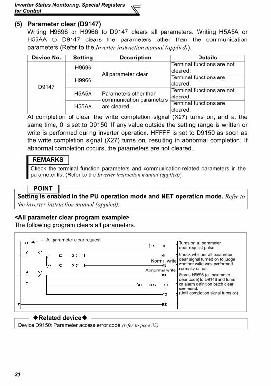
(5) Parameter clear (D9147)Writing H9696 or H9966 to D9147 clears all parameters. Writing H5A5A orH55AA to D9147 clears the parameters other than the communicationparameters (Refer to the Inverter instruction manual (applied)).
At completion of clear, the write completion signal (X27) turns on, and at thesame time, 0 is set to D9150. If any value outside the setting range is written orwrite is performed during inverter operation, HFFFF is set to D9150 as soon asthe write completion signal (X27) turns on, resulting in abnormal completion. Ifabnormal completion occurs, the parameters are not cleared.
<All parameter clear program example>The following program clears all parameters.
Device No. Setting Description Details
D9147
H9696All parameter clear
Terminal functions are not cleared.
H9966 Terminal functions are cleared.
H5A5A Parameters other than communication parameters are cleared.
Terminal functions are not cleared.
H55AA Terminal functions are cleared.
REMARKSCheck the terminal function parameters and communication-related parameters in theparameter list (Refer to the Inverter instruction manual (applied)).
POINTSetting is enabled in the PU operation mode and NET operation mode. Refer tothe inverter instruction manual (applied).
Related deviceDevice D9150: Parameter access error code (refer to page 33)
Normal write
Abnormal writeStores H9696 (all parameterclear code) to D9146 and turnson alarm definition batch clear command.(Until completion signal turns on)
All parameter clear requestTurns on all parameterclear request pulse.
Check whether all parameterclear signal turned on to judgewhether write was performednormally or not.

Inverter Status Monitoring, Special Registersfor Control
PLC
FU
NC
TIO
N
31
1
1.7.4 Inverter operation status control
(1) Inverter operation status control (D9148)Device for inverter operation status control. The operation of the inverter can becontrolled by turning on/off (1, 0) bits b0 to b11 of D9148.All bits are factory-set to "0".
Example: When 5 is set to D9148, bits b0 and b2 are 1 (ON), and STF and RHtherefore turn on to give a high-speed forward rotation command.
Device No. Name Data Access Enable ConditionD9148 Inverter operation status control Always
Note that this function is enabled in the external/NET operation mode. (Not enabled in the PUoperation mode.)
D9149 Inverter operation status control enable/disable
CAUTIONAs in the external input terminals, functions can be assigned to the bits ofD9148 using Pr.178 to Pr.189. However, no function can be assigned to SQ(sequence RUN setting: 50).
B15 B12B11 B8B7 B4B3 B00:OFF1:ON
STF (Pr.178)STR (Pr.179)RH (Pr.182)RM (Pr.181)RL (Pr.180)JOG (Pr.185)RT (Pr.183)AU (Pr.184)CS (Pr.186)MRS (Pr.187)STOP (Pr.188)RES (Pr.189)
Invalid
101000000000

Inverter Status Monitoring, Special Registers for Control
32
(2) Inverter operation status control enable/disable setting (D9149)You can enable or disable D9148 "inverter operation status control". The controlsof the corresponding bits of D9148 are enabled by turning on/off (1, 0) bits b0 tob11 of D9149. All bits are factory-set to "0".
Example: When H1F is set to D9149, bits b0 to b11 are 1 (ON), the external terminalinputs are therefore all disabled, and operation control using the inverteroperation status control (D9148) can be performed.
<Operation command setting program example>The following program example runs the inverter at high speed in forward rotationdirection.
CAUTION•When D9148 "inverter operation status control" is enabled using D9149,the control performed by external terminal inputs and the controlperformed by CC-Link remote inputs are disabled for the enabled bits.(Same as when "No functions" are set to Pr.178 to Pr.189.)
•When the terminal is made valid from PLC function, control from externalterminal is made invalid.
B15 B12B11 B8B7 B4B3 B00:OFF1:ON
STF (Pr.178)STR (Pr.179)RH (Pr.182)RM (Pr.181)RL (Pr.180)JOG (Pr.185)RT (Pr.183)AU (Pr.184)CS (Pr.186)MRS (Pr.187)STOP (Pr.188)RES (Pr.189)
Invalid
111111111111
Operation start
Operation stop
Turns on operation start pulse.
Enables all inverter operation statuscontrol enable/disable bits, anddisables external terminal inputs.
Self-holds operation start, and turnson bits 0 (STF) and 2 (RH) of inverteroperation status control, D9148.
At input of stop signal, clears inverteroperation status control, D9148,to 0 and decelerates inverter to stop.
HFFF

Inverter Status Monitoring, Special Registersfor Control
PLC
FU
NC
TIO
N
33
1
1.7.5 Inverter parameter access error (D9150)
If any value outside the setting range is written during parameter write, set frequencywrite, parameter clear, etc. from the sequence program of the inverter, or if write isperformed when write is disabled, a write alarm occurs and the corresponding alarmcode is stored into D9150.
<Parameter>The parameter No. + H8000 is stored into D9150.Example: If an error occurs during write of Pr.0 Torque boost, H8000 (H0 + H8000) is
stored into D9150.If an error occurs during write of Pr.10 DC injection brake operation frequency,H800A is stored into D9150.
<Operation mode, set frequency, alarm definition batch clear, all parameterclear>HFFFF is stored into D9150. (Normal 0)
1.7.6 Inverter status (D9151)
The running status and operating status of the inverter are stored.The corresponding bits are set according to the inverter status.
Device No. Name Data Access Enable Condition
D9150 Inverter parameter access error Always
POINTIf write is completed normally after error occurrence, D9150 is not cleared(D9150 data is held at error occurrence). When using D9150 to stop operation,etc., the user must clear it.
Device No. Name Data Access Enable Condition
D9151 Inverter status Always
B15 B8B7 B4B3 B00:OFF1:ON
Inverter running(RUN)Forward runningReverse runningUp to frequency(SU)Overload alarm(OL)Instantaneous power failure/undervoltage(IPF)Output frequency detection(FU)Alarm output(ALM)Minor fault output(LF)

Inverter Parameter Read/Write Method
34
1.8 Inverter Parameter Read/Write Method
1.8.1 Reading the inverter parameters
When reading the parameter, the parameter description is stored to D9242(D9244) bystoring the parameter number to D9241(D9243) and turning Y28 (Y2A) on. Whenreading is completed, X28 (X2A) turns ON to notify the completion. (The devicenumber within parentheses is used to read the parameter setting value fromEEPROM.)When reading the calibration parameter (Pr. 902 to Pr. 939), set the following value toD9234 (D9235) to read each calibration parameter value. 0: Setting value (Frequency/Toruque) 1: Parameter-set analog value 2: Analog value input from terminalWhen access error occurs such as "parameter does not exist", value obtained by adding the parameter number and 8000H is stored to D9150. (Refer to page 33)
Device No. Name Command CompletionData Access Enable
Condition(Operation mode)
D9241 Parameter number (RAM)
Y28 X28 AlwaysD9242 Parameter description (RAM)
D9234 Second parameter changing (RAM)
D9243 Parameter number (EEPROM)
Y2A X2A PU, NET operation mode(as in Pr.77)
D9244 Parameter description (EEPROM)
D9235 Second parameter changing (EEPROM

Inverter Parameter Read/Write Method
PLC
FU
NC
TIO
N
35
1
Inverter parameter data read timing chart
Y28(Y2A)Parameter readcommand
X28(X2A)Parameter readcompletion
D9242(D9243)Parameterread data
User sequenceprocessing
Inverterparameter
1) Read command is turned on in user sequence.
3) In user sequence, ON of read completion is confirmed and data are read from data registers D9242(D9243) and processed.
4) After completion of read, read command is turned off.
2) Inverter CPU stores inverter parameter data into data registers D9242(D9243), and turns on read completion.
5) Inverter CPU confirms that read command is off and turns off read completion.

Inverter Parameter Read/Write Method
36
1.8.2 Writing the inverter parameters
Parameter writing is performed when the parameter number is stored to D9241(D9243) and parameter writing value to D9242 (D9244), and turns ON the Y29 (Y2B).When writing is completed, X29 (X2B) turns ON to notify the completion. (The devicenumber within parentheses is used to write the parameter setting value to EEPROM.)When writing the calibration parameter (Pr. 902 to Pr. 939), set the following value toD9234 (D9235) to write each calibration parameter value. 0: Setting value (Frequency/Toruque) 1: Parameter-set analog value 2: Analog value input from terminal
As soon as the inverter parameter write completion (X29 (RAM) or X2B (EEPROM))turns on, 0 is set to D9150 on normal completion.If an error occurs during access to the parameters, e.g. if any value outside the settingrange is written or write is performed during inverter operation, the value of parameterNo. + H8000 is set to D9150 as soon as the write completion signal (X29 (RAM) orX2B (EEPROM)) turns on, resulting in abnormal completion. If abnormal completionoccurs, the parameters are not written. (For example, if an error occurs in the torqueboost, H8000 is written to D9150.)For whether inverter parameter write can be performed or not, refer to Pr.77 Parameterwrite selection .
Device No. Name Command CompletionData Access Enable
Condition (Operation mode)
D9241 Parameter number (RAM)
Y29 X29 AlwaysD9242 Parameter description (RAM)
D9234 Second parameter changing (RAM)
D9243 Parameter number (EEPROM)
Y2B X2B PU, NET operation mode(as in Pr.77)
D9244 Parameter description (EEPROM)
D9235 Second parameter changing (EEPROM
POINTInverter parameter write must be performed in the PU operation mode or NEToperation mode. (Refer to the inverter instruction manual (applied).)

Inverter Parameter Read/Write Method
PLC
FU
NC
TIO
N
37
1
Inverter parameter data write timing chart
Y29(Y2B)
X29(X2B)Parameter write completion
Inverter parameter
D9242(D9244)Parameter writedata
User sequencedata
Parameterwrite command
1) In user sequence, user data are stored into parameter write data area (D9242(D9244)).
2) Write command is turned on in user sequence.
4) After confirmation of write completion, write command is turned off.
3) Turns on when inverter CPU completes inverter parameter data write. 0 written to D9150 indicates normal completion. Any value other than 0 indicates abnormal completion.
5) Inverter CPU confirms that write command is off and turns off write completion.

User Area Read/Write Method
38
1.9 User Area Read/Write MethodInverter parameters Pr.506 to Pr.515 can be used as user parameters.Since this parameter area and the devices used with the PLC function, D110 to D119,are accessible to each other, the values set in Pr.506 to Pr.515 can be used in asequence program. The result of operation performed in the sequence program canalso be monitored using Pr.506 to Pr.515.
1.9.1 User parameter read/write methodUser parameter (Pr.506 to Pr.515) and device (D110 to D119) data can be read/writtenfreely. Data transfer between Pr.506 to Pr.515 and D110 to D119 is executedautomatically.1)User parameter write processing
When values are written to Pr.506 to Pr.515 using the FR-PU04 or computer linkcommunication, they are written to the parameter storing RAM area and EEPROMarea, and further to D110 to D119 simultaneously.
2)User parameter read processingWhen values are written to D110 to D119 from the PLC function side, they arewritten to the parameter storing RAM area (Pr.506 to Pr.515) and read using the FR-PU04/FR-PU07 or communication(RS-485 or communication option). (Since dataare not written to the EEPROM, making power-on reset returns the data to theoriginal values.)
3)Processing performed at inverter reset or power restorationWhen the inverter is reset, the Pr.506 to Pr.515 values stored in the EEPROM aretransferred to the RAM area and D110 to D119.
Device No.
Inverter Parameter
No.Name Initial
ValueSetting Range
Minimum Setting Unit Data Access
D110 to D119 506 to 515 User
parameters 0 0 to 65535 1 Always
enabled
POINTExample of using the user parameter areaWhen the timing is to be changed for machine adjustment using D110 thatstores the timer setting, setting Pr. 506 without modifying the program entersthe set data into D110, enabling adjustment.
Pr.506 to Pr.515 D110 to D119
Inverter parameters PLC function devices
Pr.506 to Pr.515(RAM)
D110 to D119
Pr.506 to Pr.515(EEPROM)
3)
3)
1)
1)
2) 2)
1)
1)FR-PU04 or RS-485communication

Analog I/O function
PLC
FU
NC
TIO
N
39
1
1.10 Analog I/O function
1.10.1 Analog inputAnalog input value of termianl 1, 2, 4 can be read from D9245 to D9247.
Actual read processing is performed at the END processing of the sequence.
1.10.2 Analog outputAnalog output from each terminal can be performed by setting value on D9251 toD9254.Output from PLC function can be performed by setting "7" in output signal selectionparameters of each terminal (terminal FM: Pr. 54, terminal AM: Pr. 158, terminal AMO,AM1: Pr. 306, Pr. 310).
Actual read processing is performed at the END processing of the sequence.
Device No. Terminal Name Setting
UnitData Access Enable
ConditionD9245 Terminal 1 input 0.1%
AlwaysD9246 Terminal 2 input 0.1%D9247 Terminal 4 input 0.1%
REMARKSFull-scale value of analog input is determined by the setting of Pr. 73 Analog input selection, Pr.267 Terminal 4 input selection. Refer to the inverter instruction manual (applied).
Device No. Terminal Name Setting
UnitData Access Enable
ConditionD9251 Terminal FM 0.1%
Always
D9252 Terminal AM 0.1%
D9253 Terminal AM0(FR-A7AY) 0.1%
D9254 Terminal AM1(FR-A7AY) 0.1%
REMARKSHigh speed pulse train output (Pr. 291) from terminal FM can be performed. (Refer to theinverter instruction manual (applied).)

Paluse train input function
40
1.11 Paluse train input functionPulse train (the number of sampling pulses) from terminal JOG is stored to D9236.When the sampling pulses overflow, make adjustment with the setting of Pr. 416 andPr. 417.
The number of sampling pulses= the number of input pulses per count cycle x Pre-scale setting value (Pr. 417) xincrements scaling factor (Pr. 416)
Parameter Name Initial Value
Setting Range Description
291Pulse train input
selection 00, 10,20 Terminal JOG1,11,21,100 Pulse train input
416 Pre-scale function selection 0 0 to 5
Pre-scale function selection (increments scaling factor)0: No function1: ×12: ×0.13: ×0.014: ×0.0015: ×0.0001
417 Pre-scale setting value 1 0 to 32767
Set the pre-scale value to calcute the number of sampling pulse when inputting the pulse train.
Device No. Name Setting Range Description
D9236 Pulse train input sampling pulse 0 to 32767 The number of pulses counted in
count cycle is stored.
D9237 Pulse train input cumulative count value L 0 to
99999999The cumulative value of the number of sampling pulses is stored.D9238 Pulse train input cumulative
count value H
D9239 Reset request of pulse train input count
0 Not clear1 Count clear
D9240 Count start of the pulse train input
0 Stop counting1 Start counting

PID control
PLC
FU
NC
TIO
N
41
1
1.12 PID controlWith PLC function, PID set point/PID deviation value, PID process value can be set bysetting Pr. 128.Performing the PID operation using the value of D9248 and D9249 as PID set point/PID deviation value, PID process value, manipulated variable is stored to D9250.When performing PID control with PLC function, "1" is set on D9255 instead of X14signal.
Parameter Name Initial Value
Setting Range Description
128 PID action selection 10
10 PID reverse action Deviation value signal input(terminal 1)11 PID forward action
20 PID reverse action Measured value (terminal 4)
Set point (terminal 2 or Pr. 133)
21 PID forward action
50 PID reverse action Deviation value signal input(LONWORKS ,
CC-Link communication)
51 PID forward action
60 PID reverse action Measured value, set point input(LONWORKS ,
CC-Link communication)
61 PID forward action
70 PID reverse action Deviation value signal input
(PLC function)71 PID forward action
80 PID reverse action Measured value,Set point
(PLC function)81 PID forward action
90 PID reverse action Deviation value signal input
(PLC function)91 PID forward action
100 PID reverse action Measured value, Set point input(PLC function)101 PID forward action
D9248
D9249
PID set point /
PID deviationPID manipulated variable D9250
or
Inverter frequency settingPID measurement
value
PID control
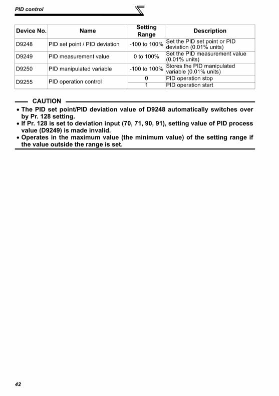
PID control
42
Device No. Name Setting Range Description
D9248 PID set point / PID deviation -100 to 100% Set the PID set point or PID deviation (0.01% units)
D9249 PID measurement value 0 to 100% Set the PID measurement value (0.01% units)
D9250 PID manipulated variable -100 to 100% Stores the PID manipulated variable (0.01% units)
D9255 PID operation control 0 PID operation stop1 PID operation start
CAUTION• The PID set point/PID deviation value of D9248 automatically switches over
by Pr. 128 setting.• If Pr. 128 is set to deviation input (70, 71, 90, 91), setting value of PID process
value (D9249) is made invalid.• Operates in the maximum value (the minimum value) of the setting range if
the value outside the range is set.

43
Inverter Operation Lock Mode Setting
1
PLC
FU
NC
TIO
N
1.13 Inverter Operation Lock Mode SettingYou can disable a sequence program from being executed until the sequence programexecution key is set to RUN (SQ signal is turned on).
POINTWhen you want to perform only inverter operation without using the PLC function,set "0" (inverter start signal enable) in this parameter.
Parameter Name initial Setting
Setting Range
Minimum Setting Unit
415 Inverter operation lock mode setting 0 0, 1 1
Setting Description
0 The inverter start signal is made valid regardless of the sequence program execution key.
1
The inverter start signal is made valid only when the sequence program execution key is set to RUN (SQ signal is turned on).When the sequence program execution key is in the STOP position (SQ signal is off), the inverter does not start if the inverter start signal STF or STR is turned on. (If the key is switched from RUN to STOP during inverter operation, the inverter is decelerated to a stop.)
CAUTION•Independently of the Pr. 77 setting, this parameter value cannot be rewrittenduring inverter operation.
•During automatic operation performed using D9148(or M9200 to M9211) in thesequence program, the inverter comes to a stop when the sequence is set to aSTOP status with "1" set in Pr.415. However, when "0" is set in Pr.415, thedevice data are held and the operation status does not change if the sequenceis set to a STOP status. (Inverter operation is continued.)
REMARKSThis parameter setting is also valid for the start signal from the operation panel or FR-PU04/FR-PU07.

44
MEMO

2. CC-Link COMMUNICATION
45
Chapter 1
Chapter 2
Chapter 3
Chapter 4
2.1 System Configuration .......................................... 462.2 CC-Link Parameters ............................................. 492.3 CC-Link I/O Specifications................................... 502.4 Buffer Memory ...................................................... 57

System Configuration
46
2.1 System Configuration
2.1.1 System configuration example(1) PLC side
Mount the "Control & Communication Link system master/local module" on themain base unit or extension base unit of the PLC CPU that will act as the masterstation.
(2) Connect the PLC CC-Link module master station and inverters by CC-Linkdedicated cables.
REMARKSRefer to the FR-A7NC indtruction manual for the CC-Link communication wiring and CC-Linkcables.
CPU AJ61
BT11
Master station
Po
wer
su
pp
lym
od
ule
Terminatingresistor
CC-Link dedicated cable
InverterInverter
Up to 42 inverterscan be connectedwhen only invertersare connected.
Power supply Motor MotorPower supply

System Configuration
CC
-Lin
k C
OM
MU
NIC
ATI
ON
47
2
2.1.2 Function block diagramHow I/O data are transferred to/from the inverter in CC-Link will be described usingfunction blocks.(1) Between the master station and inverter in the CC-Link system, link refresh is
always made at 3.5 to 18ms (512 points).(2) I/O refresh and master station's sequence program are executed asynchronously.(3) Data read from the inverter are read from the buffer memory of the CC-Link
system master/local module using the FROM instruction.(4) Data to be written to the inverter are written to the buffer memory of the CC-Link
system master/local module using the TO instruction.
1) I/O signals assigned to the CC-Link system master/local module. These signalsare used to make communication between the PLC CPU and CC-Link systemmaster/local module.
2) Input data from the inverter can be read, and output data from the inverter can bewritten. Buffer memory read/write is performed using the FROM/TO instruction ofthe sequence program. Refer to page 57 for details of the buffer memory.
3) PLC link start is commanded from the sequence program. After PLC link hasstarted, link refresh is always made asynchronously with the sequence programexecution.
4) I/O data are transferred between the CC-Link system master/local module andinverter CPU via the sequence program.
5) I/O data are transferred between the inverter CPU and sequence program. (5)indicates the operation performed when CC-Link is not used, and is irrelevant to1) to 4).)
REMARKSPrograms cannot be read/written via CC-Link communication.
CPU
InverterCC-Link module
4)
PLC
CPU
1) CC-Link module I/O signals
2) Buffer memory read/write
Inte
rface
with
PLC
Buffermemory
CC
-Lin
k in
terfa
ce 3) CC-Link dedicated cable
CC
-Lin
k in
terfa
ce
Built
-in s
eque
nce
prog
ram
5) I/O
data
Inve
rter C
PU
Input signal
Output signal

System Configuration
48
POINTThe difference between CC-Link communication (Pr. 544 = 100, 112, 114, 118)with PLC function and normal CC-Link communication (Pr. 544 =1, 2, 12, 14, 18)is indicated below.
I/O (RX, RY)
I/O (RX, RY)
RWw RWr
RWw RWr
PL
C C
PU
CC
-Lin
k m
aste
r m
odule
Inverter
Pr.544=0,1,12,14,18
Inve
rte
r C
PU
Parameter read/write, monitor, operation commands, etc. have been assigned in advance.
PL
C C
PU
CC
-Lin
k m
aste
r m
odule
Pr.544=100,112,114,118
Built-in CC-Link module
Inverter
Built-in sequenceprogram
Userassignment
Inve
rte
r C
PU
Using built-in sequence program, parameters,monitor, etc. must be assigned.Other data read/write, etc. can be assignedfreely as user areas.*Operation and speed commands have been assigned in advance.

CC-Link Parameters
CC
-Lin
k C
OM
MU
NIC
ATI
ON
49
2
2.2 CC-Link Parameters
2.2.1 CC-Link Extended Setting (Pr. 544)Remote register function can be extended.
*1 The program used for conventional series inverter (FR-A5NC) can be used.*2 When using double, quadruple and octuple settings of the CC-Link Ver.2, station data of
the master station must be set to double, quadruple and octuple also.(If the master station is CC-Link Ver.1 compatible station, the above setting can not bemade.)
Parameter Number Name Initial
ValueSetting Range DescriptionCC-Link
Ver.
544 CC-Link extended setting 0
01
Occupies one station(FR-A5NC compatible) *1
1 Occupies one station12 *2
2
Occupies one station double
14 *2 Occupies one station quadrople
18 *2 Occupies one station octuple
100 1 Occupies one station(PLC function)
112 *2
2
Occupies one station double (PLC function)
114 *2 Occupies one station quadrople (PLC function)
118 *2 Occupies one station octuple (PLC function)
REMARKSThe setting change is reflected after an inverter reset.

CC-Link I/O Specifications
50
2.3 CC-Link I/O Specifications
2.3.1 I/O signal when CC-Link Ver.1 one station is occupied (Pr. 544 = 100)
The device points usable in CC-Link communication are 32 input (RX) points (16points are available for PLC function), 32 output (RY) points (16 points are availablefor PLC function), 4 remote register (RWr) points and 4 remote register (RWw) points.
(1) Remote I/O PLC
function device
No.
Remote output device
No.Signal
PLC function device
No.
Remote input
device No.
Signal
X30 RYn0 Forward rotation command X30 RXn0 Forward runningX31 RYn1 Reverse rotation command X31 RXn1 Reverse running
X32 RYn2High-speed operation command(terminal RH function) *1
X32 RXn2 Running(terminal RUN function) *2
X33 RYn3Middle-speed operation command(terminal RM function) *1
X33 RXn3 Up to frequency(terminal SU function) *2
X34 RYn4Low-speed operation command(terminal RL function) *1
X34 RXn4 Overload alarm(terminal OL function) *2
X35 RYn5 Jog operation command (terminal JOG function) *1 X35 RXn5 Instantaneous power failure
(terminal IPF function) *2
X36 RYn6 Second function selection (terminal RT function) *1 X36 RXn6 Frequency detection
(terminal FU function) *2
X37 RYn7 Current input selection(terminal AU function) *1 X37 RXn7 Error
(terminal ABC1 function) *2
X38 RYn8Selection of automatic restart after instantaneous power failure (terminal CS function) *1
X38 RXn8 (terminal ABC2 function) *2
X39 RYn9 Output stop X39 RXn9 Pr. 313 assignment function (DO0)
X3A RYnA Start self-holding selection (terminal STOP function) *1 X3A RXnA Pr. 314 assignment function
(DO1)
X3B RYnB Reset(terminal RES function) *1 X3B RXnB Pr. 315 assignment function
(DO2) X3C RYnC
General-purpose remote input available in PLC function
X3C RXnCGeneral-purpose remote input available in PLC function
X3D RYnD X3D RXnDX3E RYnE X3E RXnEX3F RYnF X3F RXnF
RY(n+1)0
to RY(n+1)7
Reserved RX(n+1)0
to RX(n+1)7
Reserved
RY(n+1)8Not used(initial data process completion flag)
RX(n+1)8Not used(initial data process request flag)
RY(n+1)9Not used(initial data process request flag)
RX(n+1)9Not used(initial data process completion flag)
RY(n+1)A Error reset request flag RX(n+1)A Error status flag
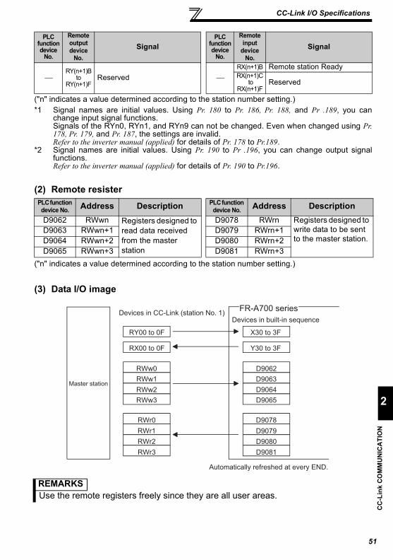
CC-Link I/O Specifications
CC
-Lin
k C
OM
MU
NIC
ATI
ON
51
2
("n" indicates a value determined according to the station number setting.) *1 Signal names are initial values. Using Pr. 180 to Pr. 186, Pr. 188, and Pr .189, you can
change input signal functions.Signals of the RYn0, RYn1, and RYn9 can not be changed. Even when changed using Pr.178, Pr. 179, and Pr. 187, the settings are invalid.Refer to the inverter manual (applied) for details of Pr. 178 to Pr.189.
*2 Signal names are initial values. Using Pr. 190 to Pr .196, you can change output signalfunctions.Refer to the inverter manual (applied) for details of Pr. 190 to Pr.196.
(2) Remote resister
("n" indicates a value determined according to the station number setting.)
(3) Data I/O image
RY(n+1)B
to RY(n+1)F
Reserved RX(n+1)B Remote station ReadyRX(n+1)C
to RX(n+1)F
Reserved
PLC function device No. Address Description PLC function
device No. Address DescriptionD9062 RWwn Registers designed to
read data received from the master station
D9078 RWrn Registers designed to write data to be sent to the master station.
D9063 RWwn+1 D9079 RWrn+1D9064 RWwn+2 D9080 RWrn+2D9065 RWwn+3 D9081 RWrn+3
REMARKSUse the remote registers freely since they are all user areas.
PLC function device
No.
Remote output device
No.Signal
PLC function device
No.
Remote input
device No.
Signal
Devices in CC-Link (station No. 1)
RY00 to 0F
RX00 to 0F
RWw0
RWw1
RWw2
RWw3
RWr0
RWr1
RWr2
RWr3
Devices in built-in sequence
X30 to 3F
Y30 to 3F
D9062
D9063
D9064
D9065
D9078
D9079
D9080
D9081
Automatically refreshed at every END.
FR-A700 series
Master station

CC-Link I/O Specifications
52
2.3.2 I/O signal when CC-Link Ver.2 double setting is selected (Pr. 544 = 112)
The device points usable in CC-Link communication are 32 input (RX) points (12points are available for PLC function), 32 output (RY) points (12 points are availablefor PLC function), 4 remote register (RWr) points and 4 remote register (RWw) points.
(1) Remote I/O PLC
function device
No.
Remote output device
No.Signal
PLC function device
No.
Remote input
device No.
Signal
X30 RYn0 Forward rotation command X30 RXn0 Forward runningX31 RYn1 Reverse rotation command X31 RXn1 Reverse running
X32 RYn2High-speed operation command(terminal RH function) *1
X32 RXn2 Running(terminal RUN function) *2
X33 RYn3Middle-speed operation command(terminal RM function) *1
X33 RXn3 Up to frequency(terminal SU function) *2
X34 RYn4Low-speed operation command(terminal RL function) *1
X34 RXn4 Overload alarm(terminal OL function) *2
X35 RYn5 Jog operation command (terminal JOG function) *1 X35 RXn5 Instantaneous power failure
(terminal IPF function) *2
X36 RYn6 Second function selection (terminal RT function) *1 X36 RXn6 Frequency detection
(terminal FU function) *2
X37 RYn7 Current input selection(terminal AU function) *1 X37 RXn7 Error
(terminal ABC1 function) *2
X38 RYn8Selection of automatic restart after instantaneous power failure (terminal CS function) *1
X38 RXn8 (terminal ABC2 function) *2
X39 RYn9 Output stop X39 RXn9 Pr. 313 assignment function (DO0)
X3A RYnA Start self-holding selection (terminal STOP function) *1 X3A RXnA Pr. 314 assignment function
(DO1)
X3B RYnB Reset(terminal RES function) *1 X3B RXnB Pr. 315 assignment function
(DO2) RYnC Monitor command RXnC Monitoring
RYnD Frequency setting command (RAM) RXnD Frequency setting completion
(RAM)
RYnE Frequency setting command (RAM, EEPROM) RXnE Frequency setting completion
(RAM, EEPROM)
RYnF Instruction code execution request RXnF Instruction code execution
completion
RY(n+1)0
to RY(n+1)7
Reserved RX(n+1)0
to RX(n+1)7
Reserved
RY(n+1)8Not used(initial data process completion flag)
RX(n+1)8Not used(initial data process request flag)
RY(n+1)9Not used(initial data process request flag)
RX(n+1)9Not used(initial data process completion flag)
RY(n+1)A Error reset request flag RX(n+1)A Error status flag
RY(n+1)B
to RY(n+1)F
Reserved RX(n+1)B Remote station ReadyRX(n+1)C
to RX(n+1)F
Reserved
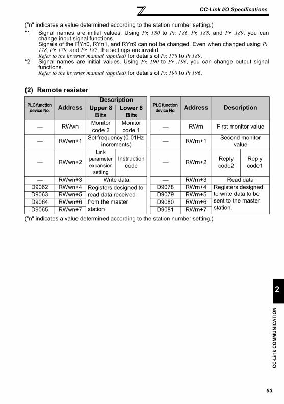
CC-Link I/O Specifications
CC
-Lin
k C
OM
MU
NIC
ATI
ON
53
2
("n" indicates a value determined according to the station number setting.) *1 Signal names are initial values. Using Pr. 180 to Pr. 186, Pr. 188, and Pr .189, you can
change input signal functions.Signals of the RYn0, RYn1, and RYn9 can not be changed. Even when changed using Pr.178, Pr. 179, and Pr. 187, the settings are invalid.Refer to the inverter manual (applied) for details of Pr. 178 to Pr.189.
*2 Signal names are initial values. Using Pr. 190 to Pr .196, you can change output signalfunctions.Refer to the inverter manual (applied) for details of Pr. 190 to Pr.196.
(2) Remote resister
("n" indicates a value determined according to the station number setting.)
PLC function device No. Address
DescriptionPLC function
device No. Address DescriptionUpper 8 Bits
Lower 8 Bits
RWwn Monitor code 2
Monitor code 1 RWrn First monitor value
RWwn+1 Set frequency (0.01Hz increments) RWrn+1 Second monitor
value
RWwn+2
Link parameter expansion
setting
Instruction code RWrn+2 Reply
code2Reply code1
RWwn+3 Write data RWrn+3 Read dataD9062 RWwn+4 Registers designed to
read data received from the master station
D9078 RWrn+4 Registers designed to write data to be sent to the master station.
D9063 RWwn+5 D9079 RWrn+5D9064 RWwn+6 D9080 RWrn+6D9065 RWwn+7 D9081 RWrn+7

CC-Link I/O Specifications
54
2.3.3 I/O signal when CC-Link Ver.2 quadruple setting is selected (Pr. 544 = 114)
The device points usable in CC-Link communication are 32 input (RX) points (12points are available for PLC function), 32 output (RY) points (12 points are availablefor PLC function), 8 remote register (RWr) points and 8 remote register (RWw) points.
(1) Remote I/O Same as when Pr. 544 = 112 ( Refer to page 52)
(2) Remote resister
("n" indicates a value determined according to the station number setting.)
PLC function device No. Address
DescriptionPLC function device No. Address DescriptionUpper 8
BitsLower 8
Bits
RWwn Monitor code 2
Monitor code 1 RWrn First monitor value
RWwn+1 Set frequency (0.01Hz increments) RWrn+1 Second monitor
value
RWwn+2
Link parameter expansion
setting
Instruction code RWrn+2 Reply
code2Reply code1
RWwn+3 Write data RWrn+3 Read data RWwn+4 Monitor code 3 RWrn+4 Third monitor value RWwn+5 Monitor code 4 RWrn+5 Fourth monitor value RWwn+6 Monitor code 5 RWrn+6 Fifth monitor value RWwn+7 Monitor code 6 RWrn+7 Sixth monitor value
D9062 RWwn+8
Registers designed to read data received from the master station
D9078 RWrn+8
Registers designed to write data to be sent to the master station.
D9063 RWwn+9 D9079 RWrn+9D9064 RWwn+A D9080 RWrn+AD9065 RWwn+B D9081 RWrn+BD9066 RWwn+C D9082 RWrn+CD9067 RWwn+D D9083 RWrn+DD9068 RWwn+E D9084 RWrn+ED9069 RWwn+F D9085 RWrn+F

CC-Link I/O Specifications
CC
-Lin
k C
OM
MU
NIC
ATI
ON
55
2
2.3.4 I/O signal when CC-Link Ver.2 octuple setting is selected (Pr. 544 = 118)
The device points usable in CC-Link communication are 32 input (RX) points (12points are available for PLC function), 32 output (RY) points (12 points are availablefor PLC function), 16 remote register (RWr) points and 16 remote register (RWw)points.
(1) Remote I/O Same as when Pr. 544 = 112 ( Refer to page 52)
(2) Remote resister
PLC function device No. Address
DescriptionPLC function
device No. Address DescriptionUpper 8 Bits
Lower 8 Bits
RWwn Monitor code 2
Monitor code 1 RWrn First monitor value
RWwn+1 Set frequency (0.01Hz increments) RWrn+1 Second monitor
value
RWwn+2
Link parameter expansion
setting
Instruction code RWrn+2 Reply
code2Reply code1
RWwn+3 Write data RWrn+3 Read data RWwn+4 Monitor code 3 RWrn+4 Third monitor value RWwn+5 Monitor code 4 RWrn+5 Fourth monitor value RWwn+6 Monitor code 5 RWrn+6 Fifth monitor value RWwn+7 Monitor code 6 RWrn+7 Sixth monitor value
RWwn+8Alarm
definition No.
H00 RWrn+8Alarm
definition No.
Alarm definition
data
RWwn+9 PID set point(0.01% increments) *1 RWrn+9 Alarm definition
(output frequency)
RWwn+A PID measured value (0.01% increments) *1 RWrn+A Alarm definition
(output current)
RWwn+B PID deviation(0.01% increments) *1 RWrn+B Alarm definition
(output voltage)
RWwn+C toruqe command / limit(0.01% increments) RWrn+C Alarm definition
(energization time) RWwn+D
H00 (Free) RWrn+D
H00 (Free) RWwn+E RWrn+E RWwn+F RWrn+F
*1 When Pr. 128 = "50, 51, 60, 61", they are valid.

CC-Link I/O Specifications
56
("n" indicates a value determined according to the station number setting.)
D9062 RWwn+10
Registers designed to read data received from the master station
D9078 RWrn+10
Registers designed to write data to be sent to the master station.
D9063 RWwn+11 D9079 RWrn+11D9064 RWwn+12 D9080 RWrn+12D9065 RWwn+13 D9081 RWrn+13D9066 RWwn+14 D9082 RWrn+14D9067 RWwn+15 D9083 RWrn+15D9068 RWwn+16 D9084 RWrn+16D9069 RWwn+17 D9085 RWrn+17D9070 RWwn+18 D9086 RWrn+18D9071 RWwn+19 D9087 RWrn+19D9072 RWwn+1A D9088 RWrn+1AD9073 RWwn+1B D9089 RWrn+1BD9074 RWwn+1C D9090 RWrn+1CD9075 RWwn+1D D9091 RWrn+1DD9076 RWwn+1E D9092 RWrn+1ED9077 RWwn+1F D9093 RWrn+1F
PLC function device No. Address
DescriptionPLC function
device No. Address DescriptionUpper 8 Bits
Lower 8 Bits

Buffer Memory
CC
-Lin
k C
OM
MU
NIC
ATI
ON
57
2
2.4 Buffer Memory2.4.1 Remote output signals
(Master module to inverter(FR-A7NC))•Input states to the remote device station are stored.•Two words are used for each station. (Do not use address 16n (n = 2(X - 1) + 1, X = station No.))
Correspondences between Master Station Buffer Memory Addresses and Station Numbers
Station No.
Buffer Memory Address
Station No.
Buffer Memory Address
Station No.
Buffer Memory Address
Station No.
Buffer Memory Address
1 160H 17 180H 33 1A0H 49 1C0H
2 162H 18 182H 34 1A2H 50 1C2H
3 164H 19 184H 35 1A4H 51 1C4H
4 166H 20 186H 36 1A6H 52 1C6H
5 168H 21 188H 37 1A8H 53 1C8H
6 16AH 22 18AH 38 1AAH 54 1CAH
7 16CH 23 18CH 39 1ACH 55 1CCH
8 16EH 24 18EH 40 1AEH 56 1CEH
9 170H 25 190H 41 1B0H 57 1D0H
10 172H 26 192H 42 1B2H 58 1D2H
11 174H 27 194H 43 1B4H 59 1D4H
12 176H 28 196H 44 1B6H 60 1D6H
13 178H 29 198H 45 1B8H 61 1D8H
14 17AH 30 19AH 46 1BAH 62 1DAH
15 17CH 31 19CH 47 1BCH 63 1DCH
16 17EH 32 19EH 48 1BEH 64 1DEH
RY F to RY 0
RY 1F to RY 10
RY11F to RY110
RY 2F to RY 20
RY 3F to RY 30
RY 4F to RY 40
RY 5F to RY 50
RY 6F to RY 60
RY 7F to RY 70
RY 8F to RY 80
RY 9F to RY 90
RY AF to RY A0
RY BF to RY B0
RY CF to RY C0
RY DF to RY D0
RY EF to RY E0
RY FF to RY F0
RY10F to RY100
RY7CF to RY7C0
RY7DF to RY7D0
RY7EF to RY7E0
RY7FF to RY7F0
Remote inputs (RY)
160H
161H
162H
163H
164H
165H
166H
167H
168H
169H
16AH
16BH
16CH
16DH
16EH
16FH
170H
171H
172H
1DBH
1DCH
1DDH
1DEH
1DFH
to
Addresses
For stationNo.1
For station No.63
Master Station
Remote device station
(Station No. 1: 1 station occupied)
X3F to X30
Inverter
RY 0F to RY 00
FR-A700 series
For stationNo.2
For stationNo.3
For stationNo.4
For stationNo.5
to
For stationNo.6
For stationNo.7
For stationNo.8
For stationNo.9
For station No.64

Buffer Memory
58
2.4.2 Remote input signals Pr.544=100(Inverter(FR-A7NC) to master module)
• Input states from the remote device station are stored.• Two words are used for each station.
(Do not use address En (n = 2(X - 1) + 1, X = station No.))
Correspondences between Master Station Buffer Memory Addresses and StationNumbers
Station No.
Buffer Memory Address
Station No.
Buffer Memory Address
Station No.
Buffer Memory Address
Station No.
Buffer Memory Address
1 E0H 17 100H 33 120H 49 140H
2 E2H 18 102H 34 122H 50 142H
3 E4H 19 104H 35 124H 51 144H
4 E6H 20 106H 36 126H 52 146H
5 E8H 21 108H 37 128H 53 148H
6 EAH 22 10AH 38 12AH 54 14AH
7 ECH 23 10CH 39 12CH 55 14CH
8 EEH 24 10EH 40 12EH 56 14EH
9 F0H 25 110H 41 130H 57 150H
10 F2H 26 112H 42 132H 58 152H
11 F4H 27 114H 43 134H 59 154H
12 F6H 28 116H 44 136H 60 156H
13 F8H 29 118H 45 138H 61 158H
14 FAH 30 11AH 46 13AH 62 15AH
15 FCH 31 11CH 47 13CH 63 15CH
16 FEH 32 11EH 48 13EH 64 15EH
FR-A700 series
Y3F to Y30
Inverter
RX 0F to RX 00RX F to RX 0
RX 1F to RX 10
RX11F to RX110
RX 2F to RX 20
RX 3F to RX 30
RX 4F to RX 40
RX 5F to RX 50
RX 6F to RX 60
RX 7F to RX 70
RX 8F to RX 80
RX 9F to RX 90
RX AF to RX A0
RX BF to RX B0
RX CF to RX C0
RX DF to RX D0
RX EF to RX E0
RX FF to RX F0
RX10F to RX100
to
RX7CF to RX7C0
RX7DF to RX7D0
RX7EF to RX7E0
RX7FF to RX7F0
Remote inputs (RX)
E0H
E1H
E2H
E3H
E4H
E5H
E6H
E7H
E8H
E9H
EAH
EBH
ECH
EDH
EEH
EFH
F0H
F1H
F2H
15BH
15CH
15DH
15EH
15FH
to
Addresses
For station No.1
For station No.2
For stationNo.63
Master station
For station No.3
For station No.4
For station No.5
For station No.6
For station No.7
For station No.8
For station No.9
For stationNo.64
Remote device station(Station No. 1: 1 station occupied)

Buffer Memory
CC
-Lin
k C
OM
MU
NIC
ATI
ON
59
2
2.4.3 Remote registers Pr.544=100(Master module to inverter(FR-A7NC))
• Data to be sent to the remote registers (RWW) of the remote device station arestored.
• Four words are used for each station.
Correspondences between Master Station Buffer Memory Addresses and Station Numbers
Station No.
Buffer Memory Address
Station No.
Buffer Memory Address
Station No.
Buffer Memory Address
Station No.
Buffer Memory Address
1 1E0H to 1E3H 17 220H to 223H 33 260H to 263H 49 2A0H to 2A3H
2 1E4H to 1E7H 18 224H to 227H 34 264H to 267H 50 2A4H to 2A7H
3 1E8H to 1EBH 19 228H to 22BH 35 268H to 26BH 51 2A8H to 2ABH
4 1ECH to 1EFH 20 22CH to 22FH 36 26CH to 26FH 52 2ACH to 2AFH
5 1F0H to 1F3H 21 230H to 233H 37 270H to 273H 53 2B0H to 2B3H
6 1F4H to 1F7H 22 234H to 237H 38 274H to 277H 54 2B4H to 2B7H
7 1F8H to 1FBH 23 238H to 23BH 39 278H to 27BH 55 2B8H to 2BBH
8 1FCH to 1FFH 24 23CH to 23FH 40 27CH to 27FH 56 2BCH to 2BFH
9 200H to 203H 25 240H to 243H 41 280H to 283H 57 2C0H to 2C3H
10 204H to 207H 26 244H to 247H 42 284H to 287H 58 2C4H to 2C7H
11 208H to 20BH 27 248H to 24BH 43 288H to 28BH 59 2C8H to 2CBH
12 20CH to 20FH 28 24CH to 24FH 44 28CH to 28FH 60 2CCH to 2CFH
13 210H to 213H 29 250H to 253H 45 290H to 293H 61 2D0H to 2D3H
14 214H to 217H 30 254H to 257H 46 294H to 297H 62 2D4H to 2D7H
15 218H to 21BH 31 258H to 25BH 47 298H to 29BH 63 2D8H to 2DBH
16 21CH to 21FH 32 25CH to 25FH 48 29CH to 29FH 64 2DCH to 2DFH
FR-A700 series
Remote registers (RWw)
1E0H
1E1H
1E2H
1E3H
1E4H
1E5H
1E6H
1E7H
1E8H
1E9H
1EAH
1EBH
1ECH
1EDH
1EEH
1EFH
Addresses
Master station
Remote device station
(Station No. 1: 1 station occupied)
RWW 0
RWW 1
RWW 2
RWW 3
RWW 4
RWW 5
RWW 6
RWW 7
RWW 8
RWW 9
RWW A
RWW B
RWW C
RWW D
RWW E
RWW F
RWW FD
RWW FC
RWW FE
RWW FF
1F0H
2DBH
2DCH
2DDH
2DEH
2DFH
to
RWW 0
RWW 1
RWW 2
RWW 3
Inverter
D9063
D9064
D9065
D9062
For stationNo.1
For stationNo.2
For stationNo.3
For stationNo.4
For stationNo.64
to

Buffer Memory
60
2.4.4 Remote registers Pr.544=100 (Inverter(FR-A7NC) to master module)
• Data sent from the remote registers (RWR) of the remote device station are stored.• Four words are used for each station.
Correspondences between Master Station Buffer Memory Addresses and StationNumbers
Station No.
Buffer Memory Address
Station No.
Buffer Memory Address
Station No.
Buffer Memory Address
Station No.
Buffer Memory Address
1 2E0H to 2E3H 17 320H to 323H 33 360H to 363H 49 3A0H to 3A3H
2 2E4H to 2E7H 18 324H to 327H 34 364H to 367H 50 3A4H to 3A7H
3 2E8H to 2EBH 19 328H to 32BH 35 368H to 36BH 51 3A8H to 3ABH
4 2ECH to 2EFH 20 32CH to 32FH 36 36CH to 36FH 52 3ACH to 3AFH
5 2F0H to 2F3H 21 330H to 333H 37 370H to 373H 53 3B0H to 3B3H
6 2F4H to 2F7H 22 334H to 337H 38 374H to 377H 54 3B4H to 3B7H
7 2F8H to 2FBH 23 338H to 33BH 39 378H to 37BH 55 3B8H to 3BBH
8 2FCH to 2FFH 24 33CH to 33FH 40 37CH to 37FH 56 3BCH to 3BFH
9 300H to 303H 25 340H to 343H 41 380H to 383H 57 3C0H to 3C3H
10 304H to 307H 26 344H to 347H 42 384H to 387H 58 3C4H to 3C7H
11 308H to 30BH 27 348H to 34BH 43 388H to 38BH 59 3C8H to 3CBH
12 30CH to 30FH 28 34CH to 34FH 44 38CH to 38FH 60 3CCH to 3CFH
13 310H to 313H 29 350H to 353H 45 390H to 393H 61 3D0H to 3D3H
14 314H to 317H 30 354H to 357H 46 394H to 397H 62 3D4H to 3D7H
15 318H to 31BH 31 358H to 35BH 47 398H to 39BH 63 3D8H to 3DBH
16 31CH to 31FH 32 35CH to 35FH 48 39CH to 39FH 64 3DCH to 3DFH
FR-A700 series
Master station
RWR 0
RWR 1
RWR 2
RWR 3
Remote registers (RWr)
2E0H
2E1H
2E2H
2E3H
2E4H
2E5H
2E6H
2E7H
2E8H
2E9H
2EAH
2EBH
2ECH
2EDH
2EEH
2EFH
Addresses
RWR 0
RWR 1
RWR 2
RWR 3
RWR 4
RWR 5
RWR 6
RWR 7
RWR 8
RWR 9
RWR A
RWR B
RWR C
RWR D
RWR E
RWR F
RWR FD
RWR FC
RWR FE
RWR FF
2F0H
3DBH
3DCH
3DDH
3DEH
3DFH
toto
For stationNo.4
Inverter
D9078
D9079
D9080
D9081
For stationNo.1
For stationNo.2
For stationNo.3
For stationNo.64
Remote device station(Station No. 1: 1 station occupied)

3. SEQUENCE PROGRAMMING
61
Chapter 1
Chapter 2
Chapter 3
Chapter 4
3.1 Overview ............................................................... 623.2 RUN and STOP Operation Processings ............. 643.3 Program Makeup .................................................. 643.4 Programming Languages .................................... 653.5 Operation Processing Method of PLC Function... 683.6 I/O Processing Method ........................................ 693.7 Scan Time.............................................................. 713.8 Numerical Values Usable in Sequence Program.. 723.9 Description of devices ......................................... 753.10 Counters C ............................................................ 833.11 Data Registers D................................................... 863.12 Special Relays, Special Registers ...................... 873.13 Function List ......................................................... 893.14 How to RUN/STOP the Built-in PLC Function
from Outside (Remote RUN/STOP) ..................... 903.15 Watchdog Timer (Operation clog up monitor
timer) ..................................................................... 923.16 Self-diagnostic Function ..................................... 933.17 Keyword Registration .......................................... 953.18 Setting of Output (Y) Status at Switching from
STOP Status to RUN Status................................. 963.19 Instruction Format................................................ 973.20 Bit Device Processing Method............................ 993.21 Handling of Numerical Value............................... 1013.22 Operation Error..................................................... 1023.23 Instructions List ................................................... 1033.24 Description of the Instructions ........................... 1103.25 Sequence Instructions......................................... 1113.26 Basic Instructions ................................................ 1403.27 Application instructions ...................................... 155

Overview
62
3.1 Overview3.1.1 Outline of Operation ProcessingsThis section outlines processings performed from when the inverter is powered onuntil a sequence program is executed.The built-in PLC function processings are roughly classified into the following threetypes.(1) Initial processing
Pre-processing for executing sequence operation. This processing is executedonly once when power is switched on or a reset is performed.(a) The inputs/outputs are reset and initialized.(b) The data memories are initialized (the bit devices are turned off and the word
devices are cleared to 0).(c) Self-diagnostic checks are made on the built-in PLC function parameter
setting, operation circuit, etc.
(2) Sequence program operation processingThe sequence program written to the built-in PLC function is executed from step 0to an END instruction.
(3) END processingPost-processing for terminating one sequence program operation processing andreturn the sequence program execution to step 0.(a) Self-diagnostic checks are performed.(b) The present values of the timers are updated and their contacts are turned
on/off, and the present values of the counters are updated and their contactsare turned on.
REMARKSThe built-in PLC function parameters can be confirmed from GX Developer. (Referto the GX Developer Operating Manual.)
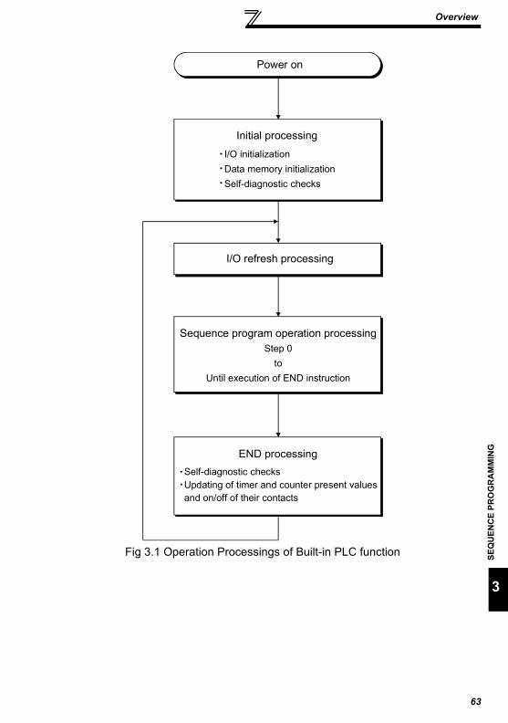
Overview
SEQ
UEN
CE
PRO
GR
AM
MIN
G
63
3
Fig 3.1 Operation Processings of Built-in PLC function
Sequence program operation processingStep 0
toUntil execution of END instruction
Power on
I/O refresh processing
Initial processing
I/O initialization Data memory initialization Self-diagnostic checks
END processing Self-diagnostic checks Updating of timer and counter present values and on/off of their contacts

64
RUN and STOP Operation Processings
3.2 RUN and STOP Operation ProcessingsThe built-in PLC function has two different operation statuses: RUN status and STOPstatus.This section explains the operation processings of the built-in PLC function in eachoperating status.(1) Operation processing in RUN status
A RUN status indicates that a sequence program repeats its operation in order ofstep 0 to END (FEND) instruction to step 0 when SQ-SD are shorted. (P.RUN is on)When entering the RUN status, the function outputs the output status saved at STOPaccording to the "STOP to (RUN-time output mode setting" (refer to page 96).
(2) Operation processing in STOP statusA STOP status indicates that a sequence program stops its operation when SQ-SD are opened or remote STOP is commanded. (P.RUN is off)When entering the STOP status, the function saves the output status and turns offall outputs. The contents of the data memories other than the outputs (Y) aremaintained.
3.3 Program Makeup(1) Program classification
The program that can be used by the built-in PLC function is a main sequenceprogram only. Microcomputer, interrupt and SFC programs cannot be used.
(2) Program capacityA program capacity indicates the capacity of the program storage memory, and itis 1k steps. Set the program capacity in the built-in PLC function parameter.
POINTIn either the RUN or STOP status, the built-in PLC function is performing I/O refreshprocessings. In the STOP status, therefore, I/O monitoring and test operation can beperformed from the peripheral device.

Programming Languages
SEQ
UEN
CE
PRO
GR
AM
MIN
G
65
3
3.4 Programming LanguagesThe built-in PLC function has two different programming methods: one that usesladders and the other that uses dedicated instructions.• Programming that uses ladders is performed in the relay symbolic language. *1• Programming that uses dedicated instructions is performed in the logic symbolic
language. *2Whether the relay symbolic language or logic symbolic language is used, the sameprogram is created.
3.4.1 Relay symbolic language (Ladder mode)The relay symbolic language is based on the concept of a relay control circuit.You can perform programming in the representation close to the sequence circuit ofrelay control.(1) Ladder block
A ladder block is the minimum unit for performing sequence program operation. Itstarts with the left hand side vertical bus and ends with the right hand side verticalbus.
Fig 3.2 Ladder Blocks
REMARKS*1. When using GX Developer for programming, perform programming in the "ladder mode".*2. When using GX Developer for programming, perform programming in the "list mode".
Right hand side vertical bus
Ladder blocks
Left hand side vertical bus
Step number
* X0 to X5: Indicate inputs. Y10 to Y14: Indicate outputs.

Programming Languages
66
(2) Sequence program operation methodSequence program operation repeats execution from a ladder block at step 0 toan END instruction.In a single ladder block, operation is performed from the left hand side verticalbus to the right, and from the top to the bottom.
Fig 3.3 Operation Processing Sequence
Beginning of one ladder block
Operation from left to right
End of one ladder block
Operation from left to rightExecution returns to step 0 when END instruction is executed.
* 1) to 17) indicate the sequence of program operation.
1) 2) 7) 8) 9)
10)
3) 4)5)
6)
11) 13) 14)
12)
15)
16)
17)
Operation from top to bottom
Operation from top to bottom
END
End of one ladder block
Beginning of one ladder block
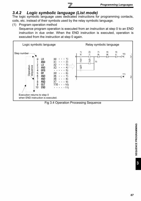
Programming Languages
SEQ
UEN
CE
PRO
GR
AM
MIN
G
67
3
3.4.2 Logic symbolic language (List mode)The logic symbolic language uses dedicated instructions for programming contacts,coils, etc. instead of their symbols used by the relay symbolic language.(1) Program operation method
Sequence program operation is executed from an instruction at step 0 to an ENDinstruction in due order. When the END instruction is executed, operation isexecuted from the instruction at step 0 again.
Fig 3.4 Operation Processing Sequence
Logic symbolic language Relay symbolic language
Step number
Ope
rati o
n se
que n
ce
Execution returns to step 0 when END instruction is executed.
1)
1) 2) 7) 8) 9)10)
3) 4)5)
6)
11)
2)3)4)5)6)7)8)9)
10)11)

68
Operation Processing Method of PLC Function
3.5 Operation Processing Method of PLC FunctionThe operation processing method is the repeated operation of a stored program.(1) Stored program system
1) In a stored program system, a sequence program to be operated is stored inthe internal memory beforehand.
2) When sequence program operation is executed, the sequence program storedin the built-in PLC function is read to the CPU instruction by instruction toexecute the operation, and the corresponding devices are controlled accordingto the results.
(2) Repeated operation systemIn a repeated operation system, a sequence of operations is repeated.The built-in PLC function repeats the following processings.1) The built-in PLC function executes the sequence program stored in the
internal memory from step 0 in due order.2) When the END instruction is executed, internal processings, such as timer/
counter present value updating and self-diagnostic checks, are performed, andthe execution returns to step 0 of the sequence program again.
Fig 3.5 Operation Processing Method of Built-in PLC Function
REMARKSA processing from step 0 to next step 0 or from END to next END is called one scan.Therefore, one scan is the sum of the processing time of a user-created program (step 0 toEND) and the internal processing time of the built-in PLC function.
Step 0Step 1Step 2
END
Built-in sequence function repeats this operation.
Timer/counter present value updating Self-diagnostic checks, etc.

69
I/O Processing Method
3
SEQ
UEN
CE
PRO
GR
AM
MIN
G
3.6 I/O Processing MethodThe control system is a refresh system.3.6.1 What is refresh system?In the refresh system, control input terminal changes are batch-imported into the inputdata memory of the CPU before execution of each scan, and the data of this input datamemory are used as the input data for operation execution.Each program operation result of the output (Y) is output to the output data memory,and after the END instruction is executed, the contents of the output data memory arebatch-output from the control output terminal.
Fig 3.6 I/O Data Flows in Refresh System
• Input refreshBefore execution of step 0, input data are batch-read from the input module (1))and stored into the input (X) data memory.
• Output refreshBefore execution of step 0, the data of the output (Y) data memory (2)) are batch-output to the output module.
• When input contact instruction is executedInput data are read from the input (X) data memory (3)) and the sequenceprogram is executed.
• When output contact instruction is executedOutput data are read from the output (Y) data memory (4)) and the sequenceprogram is executed.
• When output OUT instruction is executedThe operation result (5) of the sequence program is stored into the output (Y) datamemory.
CPU (Central Processing Unit)
1)
2)
4)
5)Y20Y22
X0
3) Input (X) data memory
Output (Y) data memory
Control input terminal
At input refresh
Control output terminal
At output refresh
PLC

70
I/O Processing Method
3.6.2 Response delay in refresh systemThis section describes a delay of an output change in response to an input change.An output change in response to an input change has a delay of up to two scans asshown in Fig. 2.6.
Fig 3.7 Output Y Change in Response to Input X Change
Ladder example
When Y1E turns on earliest
The Y1E output turns on earliest when the control input terminal turns from OFF toON immediately before a refresh. X5 turns on at an input refresh, Y1E turns on atstep 0, and the control output terminal turns on at an output refresh after execution ofthe END instruction.In this case, therefore, a delay of a control output terminal change in response to acontrol input terminal change is one scan.
When Y1E turns on latest
The Y1E output turns on latest when the control input terminal turns from OFF to ONimmediately after a refresh. X5 turns on at the next input refresh, Y1E turns on atstep 0, and the control output terminal turns on at an output refresh after execution ofthe END instruction.In this case, therefore, a delay of a control output terminal change in response to acontrol input terminal change is two scans.
In this ladder, output Y1E turns on when input X5 turns on.
OFF
OFF
OFFON
ON
ON
OFFON
Input refresh Input refresh Output refresh0 END END0 56 0
(Minimum 1 scan)
Control output terminal
Y1E
X5
Control input terminal
Delay
OFF
OFF
OFFON
ON
ON
OFFON
Input refresh Input refresh Output refresh0 END END0 56 0
Delay
(Maximum 2 scans)
Control output terminal
Y1E
X5
Control input terminal
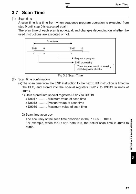
71
Scan Time
3
SEQ
UEN
CE
PRO
GR
AM
MIN
G
3.7 Scan Time(1) Scan time
A scan time is a time from when sequence program operation is executed fromstep 0 until step 0 is executed again.The scan time of each scan is not equal, and changes depending on whether theused instructions are executed or not.
Fig 3.8 Scan Time(2) Scan time confirmation
(a)The scan time from the END instruction to the next END instruction is timed inthe PLC, and stored into the special registers D9017 to D9019 in units of10ms.1) Data stored into special registers D9017 to D9019
• D9017 ........... Minimum value of scan time• D9018 ........... Present value of scan time• D9019 ........... Maximum value of scan time
2) Scan time accuracyThe accuracy of the scan time observed in the PLC is 10ms.For example, when the D9018 data is 5, the actual scan time is 40ms to60ms.
Scan time
END END0 0
Sequence program
END processingTimer/counter count processingSelf-diagnostic checks

Numerical Values Usable in Sequence Program
72
3.8 Numerical Values Usable in Sequence ProgramThe built-in PLC function represents numerical values, alphabets and other data in twostatuses: 0 (OFF) and 1 (ON).The data represented by these 0s and 1s are called BIN (binary code).The built-in PLC function can also use HEX (hexadecimal code) that represents BINdata in blocks of four bits.Table 2.1 indicates the numerical representations of BIN, HEX and decimal code.
Table 3.1 Numerical Representations of BIN, HEX and Decimal Code
DEC (Decimal Code)
HEX (Hexadecimal Code)
BIN(Binary Code)
0123••••••91011121314151617••••••
47
0123••••••9ABCDEF1011••••••
2F
01
1011••••••
1001101010111100110111101111
1000010001
••••••
101111
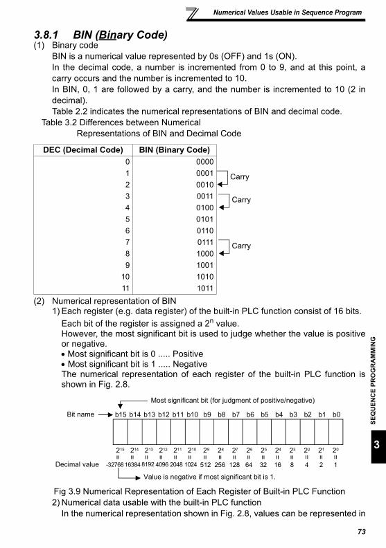
Numerical Values Usable in Sequence Program
SEQ
UEN
CE
PRO
GR
AM
MIN
G
73
3
3.8.1 BIN (Binary Code)(1) Binary code
BIN is a numerical value represented by 0s (OFF) and 1s (ON).In the decimal code, a number is incremented from 0 to 9, and at this point, acarry occurs and the number is incremented to 10.In BIN, 0, 1 are followed by a carry, and the number is incremented to 10 (2 indecimal).Table 2.2 indicates the numerical representations of BIN and decimal code.
Table 3.2 Differences between Numerical Representations of BIN and Decimal Code
(2) Numerical representation of BIN1) Each register (e.g. data register) of the built-in PLC function consist of 16 bits.
Each bit of the register is assigned a 2n value.However, the most significant bit is used to judge whether the value is positiveor negative.• Most significant bit is 0 ..... Positive• Most significant bit is 1 ..... NegativeThe numerical representation of each register of the built-in PLC function isshown in Fig. 2.8.
Fig 3.9 Numerical Representation of Each Register of Built-in PLC Function2) Numerical data usable with the built-in PLC function
In the numerical representation shown in Fig. 2.8, values can be represented in
DEC (Decimal Code) BIN (Binary Code)0 00001 00012 00103 00114 01005 01016 01107 01118 10009 1001
10 101011 1011
Carry
Carry
Carry
Value is negative if most significant bit is 1.
b15 b14 b13 b12 b11 b10 b9 b8 b7 b6 b5 b4 b3 b2 b1 b0
Most significant bit (for judgment of positive/negative)
214 213 212 211 210 29 28 27 26 25 24 23 22 21 20215
16384 8192 4096 2048 1024 512 256 128 64 32 16 8 4 2 1-32768
Bit name
Decimal value
= = = = = = = = = = = = = = = =

Numerical Values Usable in Sequence Program
74
the range -32768 to 32767.Therefore, each register of the built-in PLC function can store any valuebetween -32768 and 32767.
3.8.2 HEX (HEX Decimal)(1) HEX
HEX represents four bits of BIN data as one digit.Using four bits in BIN, you can represent 16 values from 0 to 15.Since HEX represents any of 0 to 15 in a single digit, 9 is followed by alphabets A(instead of 10), B (11)..., and F (15) is followed by a carry.Refer to page 72 for the correspondences between BIN, HEX and decimal code.
(2) Numerical representation of HEXEach register (e.g. data register) of the built-in PLC function consist of 16 bits.Therefore, the value that can be stored into each register is represented as any of0 to HFFFF in HEX.
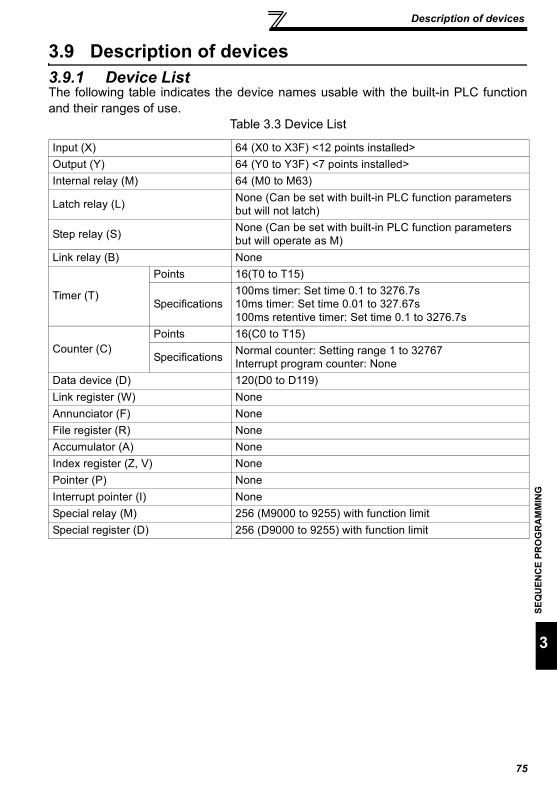
75
Description of devices
3
SEQ
UEN
CE
PRO
GR
AM
MIN
G
3.9 Description of devices3.9.1 Device ListThe following table indicates the device names usable with the built-in PLC functionand their ranges of use.
Table 3.3 Device List
Input (X) 64 (X0 to X3F) <12 points installed>Output (Y) 64 (Y0 to Y3F) <7 points installed>Internal relay (M) 64 (M0 to M63)
Latch relay (L) None (Can be set with built-in PLC function parameters but will not latch)
Step relay (S) None (Can be set with built-in PLC function parameters but will operate as M)
Link relay (B) None
Timer (T)
Points 16(T0 to T15)
Specifications100ms timer: Set time 0.1 to 3276.7s10ms timer: Set time 0.01 to 327.67s100ms retentive timer: Set time 0.1 to 3276.7s
Counter (C)Points 16(C0 to T15)
Specifications Normal counter: Setting range 1 to 32767Interrupt program counter: None
Data device (D) 120(D0 to D119)Link register (W) NoneAnnunciator (F) NoneFile register (R) NoneAccumulator (A) NoneIndex register (Z, V) NonePointer (P) NoneInterrupt pointer (I) NoneSpecial relay (M) 256 (M9000 to 9255) with function limitSpecial register (D) 256 (D9000 to 9255) with function limit

Description of devices
76
3.9.2 Inputs, Outputs X, YInputs and outputs are devices designed to transfer data between the inverter andexternal devices.Inputs provide ON/OFF data given to the corresponding control input terminals fromoutside the inverter. In a program, they are used as contacts (normally open, normallyclosed contacts) and the source data of basic instructions. Outputs are used when theoperation results of a program are output from the control output terminals to outsidethe inverter.
Fig 3.10 Inputs (X), Outputs (Y)
1
Inputs (X) Sequence operation
Outputs (Y)
Signal lamp
Contactor
InverterPushbutton switch
Select switch
Digital switch
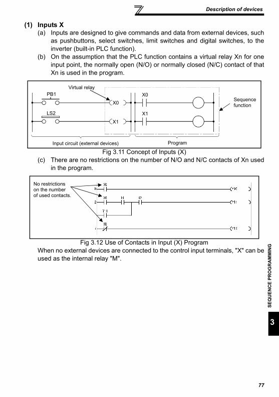
Description of devices
SEQ
UEN
CE
PRO
GR
AM
MIN
G
77
3
(1) Inputs X(a) Inputs are designed to give commands and data from external devices, such
as pushbuttons, select switches, limit switches and digital switches, to theinverter (built-in PLC function).
(b) On the assumption that the PLC function contains a virtual relay Xn for oneinput point, the normally open (N/O) or normally closed (N/C) contact of thatXn is used in the program.
Fig 3.11 Concept of Inputs (X)(c) There are no restrictions on the number of N/O and N/C contacts of Xn used
in the program.
Fig 3.12 Use of Contacts in Input (X) ProgramWhen no external devices are connected to the control input terminals, "X" can beused as the internal relay "M".
LS2
PB1
X0
X1X1
X0Virtual relay
Sequence function
Input circuit (external devices) Program
No restrictions on the number of used contacts.

Description of devices
78
(2) Outputs Y(a) Outputs are designed to output the control results of a program to outside the
inverter (signal lamps, digital indicators, magnetic switches (contactors),solenoids, etc.).
(b) An output can be exported to outside the inverter as equivalent to one N/Ocontact.
(c) There are no restrictions on the number of N/O and N/C contacts of outputYn used in the program, if they are used within the program capacity range.
Fig 3.13 Concept of Outputs (Y)When no external devices are connected to the control output terminals, "Y" canbe used as the internal relay "M".
M11
Load
No restrictions on the number of used contacts.Sequence function
Program Output circuit (external devices)

79
Description of devices
3
SEQ
UEN
CE
PRO
GR
AM
MIN
G
3.9.3 Internal Relays MInternal relays are auxiliary relays that are used in the PLC function and cannot latchdata (backup for power failure).All internal relays are turned off when:• Power is switched from off to on; or• Reset is performed.
There are no restrictions on the number of contacts (N/O and N/C contacts) used inthe program.Use outputs (Y) when outputting the operation results of the sequence program tooutside the inverter.
Fig 3.14 Internal Relay
When X0 turns from OFF to ON, M0 (internal relay) is set (turned on).
M0 may only be turned on in sequence function and cannot be output to outside.
ON/OFF data of M0 is output to outside.
No restrictions on the number of used contacts.

Description of devices
80
3.9.4 Timers TThe timers of the PLC function are count up timers.The count up timer starts timing the present value when its coil turns on, and thecontact of that timer turns on when the present value reaches the setting (time-out).
3.9.5 100ms, 10ms and 100ms retentive timers(1) 100ms and 10ms timers
The timer starts timing the present value when its coil turns on, and the presentvalue is reset to 0 and the contact turns off when the coil turns off.
Fig 3.15 Timing Chart
Ladder example
Timing chart
REMARKS100ms, 10ms and 100ms retentive timers can be changed using the built-in PLC functionparameter. (The default is a 100ms timer.)Since the FR-C500 has 8 timers (T0 to T7), it can use only any one type of 100ms, 10ms and100ms retentive timers.
When input X5 turns on, T2 coil turns on and timer times 5s. (T2 is 100ms timer.)
Setting
ON
5s
OFFT2 contact
Timer present value
T2 coil
X5 OFFON
OFFON
OFF
OFFON
OFF
OFF OFFON
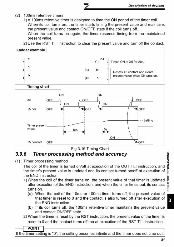
Description of devices
SEQ
UEN
CE
PRO
GR
AM
MIN
G
81
3
(2) 100ms retentive timers1) A 100ms retentive timer is designed to time the ON period of the timer coil.
When its coil turns on, the timer starts timing the present value and maintainsthe present value and contact ON/OFF state if the coil turns off.When the coil turns on again, the timer resumes timing from the maintainedpresent value.
2) Use the RST T instruction to clear the present value and turn off the contact.
Fig 3.16 Timing Chart3.9.6 Timer processing method and accuracy(1) Timer processing method
The coil of the timer is turned on/off at execution of the OUT T instruction, andthe timer's present value is updated and its contact turned on/off at execution ofthe END instruction.1) When the coil of the timer turns on, the present value of that timer is updated
after execution of the END instruction, and when the timer times out, its contactturns on.(a) When the coil of the 10ms or 100ms timer turns off, the present value of
that timer is reset to 0 and the contact is also turned off after execution ofthe END instruction.
(b) If its coil turns off, the 100ms retentive timer maintains the prevent valueand contact ON/OFF state.
2) When the timer is reset by the RST instruction, the present value of the timer isreset to 0 and the contact turns off too at execution of the RST T instruction.
Ladder example
Timing chart
POINTIf the timer setting is "0", the setting becomes infinite and the timer does not time out.
Times ON of X5 for 20s.
Resets T5 contact and clears present value when X6 turns on.
15s
Setting
ON
5s
OFFT5 contact
Timer present value
T5 coil
X5 OFF
ON
OFF
ON
OFF
OFF
ON
OFF
OFF OFF
ON

Description of devices
82
(2) Present value update timing and accuracy in refresh system1) The timer accuracy is +2 scan times independently of the used timer and scan
time.2) The following shows the present value update timing and accuracy when the
10ms timer is used in a program where the scan time is 10ms or more.
Fig 3.17 Timer Timing MethodIn Fig. 3.8, the time-out period of the 10ms timer T3 has the following errors.
*1 .......... 10ms timer error (+1 scan time)*2 .......... Error produced by timer's input condition ON timing and OUT
T instruction's program position (+1 scan time)The accuracy is +2 scan time (+0.05s in Fig. 3.8)
3) When the timer times out, its contact remains on until END even if the coil turnsoff, and turns off at execution of the END instruction.
Ladder example
Timer timing method
T3 contact turns on 6s after X0 turnson. (T3 is 10ms timer.)
OUTT3
OUTT3
OUTT3END END END END END
OUTT3
END
Scan time 25ms
When external input turns on in hatched range
*2 6000ms
*1
1 2 1 2 3 1 2 1 2 1 2 3
2 3 2 2 3
X0
T3 coil
T3 contact
10ms timertiming
Timing set at END
T3 present value
OFF
OFF
ON
ON
ON
600 appears when monitored on peripheral device.
25ms 25ms 25ms 25ms
OFF
1 scan0
1 scan0
0 3 3 3 2 5 597 2 599 599 3 602

Counters C
SEQ
UEN
CE
PRO
GR
AM
MIN
G
83
3
3.10 Counters CThe counters of the built-in PLC function are up counters.An up counter stops counting and its contact turns on when the count value reachesthe setting.(1) Count processing
1) The coil of the counter is turned on/off at execution of the OUT C instruction,and its present value is updated and its contact turns on after execution of theEND instruction.
2) The counter counts on detection of the leading edge (OFF to ON) of the coil. Itdoes not count if the coil remains on.
(2) Counter resetting1) The count value is not cleared even if the coil turns off. Use the RST C
instruction to clear the count value and turn off the contact.2) When the counter is reset by the RST instruction, the present value and
contact of the counter are cleared at execution of the RST instruction.
Fig 3.18 Count Ladder
Ladder example
C0 counts on leading edge (OFF to ON) of input X5.
Resets C0 when input X6 turns on.
Input condition
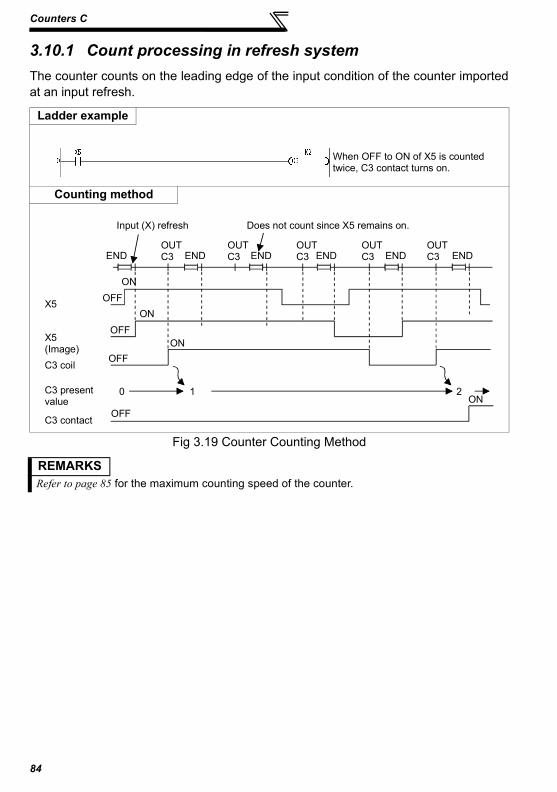
Counters C
84
3.10.1 Count processing in refresh systemThe counter counts on the leading edge of the input condition of the counter importedat an input refresh.
Fig 3.19 Counter Counting Method
Ladder example
Counting method
REMARKSRefer to page 85 for the maximum counting speed of the counter.
When OFF to ON of X5 is counted twice, C3 contact turns on.
Input (X) refresh
END ENDOUTC3
OUTC3 END
OUTC3 END
OUTC3 END
OUTC3 END
21
OFFON
OFFON
OFFON
OFF
0ON
X5
X5(Image)C3 coil
C3 present value
C3 contact
Does not count since X5 remains on.

Counters C
SEQ
UEN
CE
PRO
GR
AM
MIN
G
85
3
3.10.2 Maximum counting speed of counterThe maximum counting speed of the counter is determined by the scan time, and thecounter can count only when the ON/OFF period of the input condition is longer thanthe scan time.
REMARKSThe duty n is a percent (%) ratio of ON/OFF period to (ON + OFF period) of the count inputsignal.
Maximum counting speed Cmax 100n
ts1 [times/s] n: Duty (%)
ts: Scan time [s]
Count input signal OFF
ON
T1 T2
100[%]n T1 T2
T1
100[%]n T1 T2
T2
When T1 T2
When T1 T2
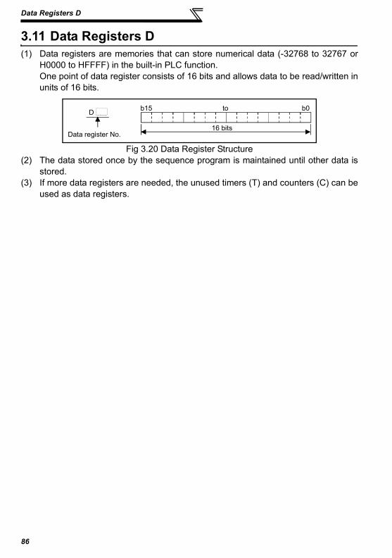
86
Data Registers D
3.11 Data Registers D(1) Data registers are memories that can store numerical data (-32768 to 32767 or
H0000 to HFFFF) in the built-in PLC function.One point of data register consists of 16 bits and allows data to be read/written inunits of 16 bits.
Fig 3.20 Data Register Structure(2) The data stored once by the sequence program is maintained until other data is
stored.(3) If more data registers are needed, the unused timers (T) and counters (C) can be
used as data registers.
b15 b0to
16 bits
D
Data register No.
Special Relays, Special Registers
SEQ
UEN
CE
PRO
GR
AM
MIN
G
87
3
3.12 Special Relays, Special RegistersSpecial relays and special registers are internal relays and data registers, respectively,whose applications are predetermined by the built-in PLC functions.They have the following main applications.(1) Sequence operation check
The special relays and special registers can be used to: (a)Check the operating status (RUN/STOP) (b)Detect a fault by the self-diagnostic function (c)Detect an operation error (d)Check the scan time
(2) Timing contactThere are special relays that can be used in a sequence program and differ inoperating status. (a)Normally ON/OFF flag (b)RUN flag (OFF for 1 scan) (c)Initial processing flag (ON for 1 scan)
REMARKSFor the special relays and special registers usable with the built-in PLC function, refer to page 10.

Special Relays, Special Registers
88
Table3.4 Special Relay Application List
Item Special Relay Application/Description
Initialprocessing flag(1 scan ON)
M9038
(1)This relay turns on for one scan when the built-in PLC function switches from STOP to RUN.
(2)Using M9038, you can create a sequence program to be executed only once without using the PLS instruction at switching from STOP to RUN.
Normal OFF flag M9037 This relay remains off while power is on.
Can be used to temporarily disable execution for debugging, etc.
Normally ON flag M9036
This relay is on while power is on.Can be used to create a program to be executed only once after power-on.
RUN flag M9039
This relay turns on at the second scan of the sequence program when SQ-SD are shorted.
ONM9038 OFF
Switching from STOP to RUN
0Sequence program
1 scan
END/0 END/0 END/0 END/0
M9038Initial processing program
M9039 OFF
RUN
0Sequence program
END/0
ON

89
Function List
3
SEQ
UEN
CE
PRO
GR
AM
MIN
G
3.13 Function ListFunction Description
Remote RUN/STOP•This function performs remote RUN/STOP from outside the
inverter when SQ-SD are shorted (PLC function in RUN status (P.RUN lit)).
Watchdog timer variable(10 to 2000ms)
•The watchdog timer is an internal timer of the sequencefunction designed to detect hardware or program faults and can be changed in setting.
Self-diagnostic function•The built-in PLC function itself diagnoses faults and performs
fault detection, indication, built-in sequencefunction stop, etc.
STOP to RUN-time output setting
•This setting is made to determine the output (Y) state when the function has switched from the STOP status to the RUN status.
Keyword registration •This setting is made to inhibit read/interrupt of a program (parameters and main/sub program) and comments.
CAUTIONThe following functions are unavailable.Constant scan, latch (backup for power failure), PAUSE, status latch, sampling trace,step run, clock, interrupt processing, comment, microcomputer mode, print titleregistration, annunciator display mode, ERROR LED priority setting

How to RUN/STOP the Built-in PLC Function from Outside (Remote RUN/STOP)
90
3.14 How to RUN/STOP the Built-in PLC Function from Outside (Remote RUN/STOP)
The built-in PLC function is RUN/STOPped by shorting/opening SQ-SD.Remote RUN/STOP is to RUN/STOP the built-in PLC function from outside theinverter with SQ-SD shorted (RUN status).(1) Applications of remote RUN/STOP
In the following cases, the function can be RUN/STOPped by remote operationusing remote RUN/STOP.1) When the inverter is out of reach.2) When the inverter in a control box is RUN/STOPped from outside the control box.
(2) Operation performed at remote RUN/STOPThe operation of the sequence program for performing remote RUN/STOP is asdescribed below.• Remote STOP.......The function enters the STOP status after the sequence
program is executed up to the END instruction.• Remote RUN ........When remote RUN is performed after the function has been
put in the "STOP status" by remote STOP, the functionenters the RUN status again and executes the sequenceprogram from step 0.
(3) Remote RUN/STOP methodThere are the following remote RUN/STOP methods.1) Setting using built-in PLC function parameter (using contact)
Remote RUN/STOP can be performed by turning the remote RUN contact off/on.For example, this method can be used to STOP the PLC function with theemergency stop contact.• When the remote RUN contact turns off, the function enters the "RUN" status.• When the remote RUN contact turns on, the function enters the "STOP"
status.
Fig 3.21 Timing Chart for RUN/STOP Using Remote RUN Contact
POINTSetting of remote RUN contact built-in PLC function parameterX0 to X1F can be set as the remote RUN contacts.(Refer to the GX Developer manual for details.)
Remote RUN contact(External input terminal)
OFFON
RUNSTOP
Built-in sequence function:
RUN/STOP status
Step 0 END Step 0 END0
STOP status
SQ terminal

How to RUN/STOP the Built-in PLC Functionfrom Outside (Remote RUN/STOP)
SEQ
UEN
CE
PRO
GR
AM
MIN
G
91
3
2) Method using GX DeveloperRUN/STOP can be performed by remote RUN/STOP operation from GXDeveloper.For example, this method can be used to STOP the function for sequenceprogram write in a place where the inverter is out of reach.
Fig 3.22 Timing Chart for RUN/STOP Using GX Developer(4) Instructions
Note the following points since the built-in PLC function gives priority to STOP.• The built-in PLC function enters the STOP status when remote STOP is
performed from any of the remote RUN contact, GX Developer, etc.• To place the built-in PLC function in the RUN status again after it has been put
in the STOP status by remote STOP, all external factors (remote RUN contact,GX Developer, etc.) for remote STOP must be set to RUN.
REMARKSWhat are RUN and STOP statuses?•RUN status............. Status where a sequence program is repeating operation from step 0 to
END instruction.•STOP status .......... Status where sequence program operation is at a stop and the outputs
(Y) are all off.
Remote STOP command OFF
ON
GX Developer
RUN/STOP status
Step 0 END Step 0 END0
STOP status
ON
OFF
RUN
STOP
Remote RUN command

92
Watchdog Timer (Operation clog up monitor timer)
3.15 Watchdog Timer (Operation clog up monitor timer)(1) Watchdog timer
A watchdog timer is the internal timer of the built-in PLC function designed todetect hardware or sequence program faults.Its default value is set to 200ms.
(2) Watchdog timer resettingThe built-in PLC function resets the watchdog timer before execution of step 0(after execution of END processing).When the built-in PLC function operates properly and the END instruction isexecuted within the setting in the sequence program, the watchdog timer doesnot time out.If the hardware fault of the built-in PLC function occurs or the scan time of thesequence program is too long to execute the END instruction within the setting,the watchdog timer times out.
Fig 3.23 Watchdog Timer Resetting(3) Processing performed when watchdog timer times out
If the scan time exceeds the watchdog timer setting, a watchdog timer erroroccurs and:1) The built-in PLC function turns off all outputs.2) The P.RUN LED goes off or flickers.3) M9008 turns on and the error code is stored into D9008.
REMARKSThe watchdog timer setting can be changed by built-in PLC function parameter setting of GXDeveloper. (Refer to the GX Developer manual for details.)
Sequence program
END 00
WDT resetting(Internal processing)
Internal processing time
Excess of scan time over settingresults in watchdog timer error.

Self-diagnostic Function
SEQ
UEN
CE
PRO
GR
AM
MIN
G
93
3
3.16 Self-diagnostic FunctionThe self-diagnostic function diagnoses faults by the built-in PLC function itself.(1) Self-diagnostic timing
The self-diagnostic function is performed at power-on, at reset, at execution ofany instruction, or at execution of the END instruction.1) At power-on, at reset
Whether operation can be executed or not is diagnosed.
2) At execution of any instructionAn error occurs if the operation of any instruction in the sequence program isnot executed properly.
3) At execution of END instructionOperation clog up monitor timer
(2) Operation mode at fault detectionThere are two different PLC operation modes at detection of a fault by the self-diagnostic: operation stop mode and operation continuation mode.The operation continuation mode includes a fault that enables operation to bestopped by built-in PLC function parameter setting. (Refer to page 94)1) If an operation stop error is detected by the self-diagnostic, operation is
stopped and outputs (Y) are all turned off as soon as the error is detected. Theother devices maintain their states at occurrence of the error.
2) If an operation continuation error is detected, only the faulty program part is notexecuted and the program at the next step is executed.
(3) Error definition checkingWhen M9008 (self-diagnostic error) turns on at detection of an error, the errorcode is stored into D9008 (self-diagnostic error). Especially in the continuationmode, use it in the program to prevent a mechanical system malfunction.For the errors detected by the self-diagnostic, refer to the error code list on page172.
CAUTIONFor the LD, AND, OR, logical comparison operation, and OUT instructions, the setdevices are always checked. For the other instructions (SET, RST, MOV, etc.), acheck is made as soon as the execution condition holds and the instruction isready to be executed.

Self-diagnostic Function
94
3.16.1 Error-time operation mode
The built-in PLC function allows you to set whether the sequence program operationwill be stopped or continued at occurrence of an operation error.Use the built-in PLC function parameter to set whether operation will be stopped orcontinued.
Default value of error-time operation modeThe following table indicates the default value (initial value) of the error-timeoperation mode and the status of the built-in PLC function.
Table 3.5 Error-time Operation Mode
Error DefinitionCPU Status
Operation P.RUN LED
Special relays
turned on
Special registers for data storage
Self-diagnostic error No. (D9008)Default value
Operation error
An error occurred in the sequence program, e.g. an attempt was made to make BCD conversion of any value outside the range 0 to 9999 (or 0 to 99999999).
Continuation Flicker M9010M9011
D9010D9011 50

95
Keyword Registration
3
SEQ
UEN
CE
PRO
GR
AM
MIN
G
3.17 Keyword RegistrationThe keyword is designed to inhibit the read and rewrite of the program and commentsin the built-in PLC function using GX Developer.(1) Read/write from built-in PLC function where keyword has been registered
When the keyword has been registered, the built-in PLC function parameters,main program and comments cannot be read/written from the built-in PLCfunction to the GX Developer device unless the keyword registered to the built-inPLC function is entered.
(2) Registration and cancel of keywordA keyword of up to six digits can be set in hexadecimal (0 to 9, A to F).Make built-in PLC function parameter setting to register or cancel the keyword.

96
Setting of Output (Y) Status at Switching from STOP Status to RUN Status
3.18 Setting of Output (Y) Status at Switching from STOP Status to RUN Status
When the RUN status is switched to the STOP status, the outputs (Y) in the RUNstatus are stored into the built-in PLC function.Using the built-in PLC function parameter, you can set whether the outputs (Y) will beoutput again or will be output after execution of operation when the STOP status isswitched to the RUN status.
"Output (Y) status at STOP is output"The sequence program operation is performed after the output (Y)status at the time of entering the STOP status is output.
"Outputs (Y) are cleared (output one scan later)"The outputs (Y) are all cleared, and after execution of the sequenceprogram operation, the outputs are provided.
Fig 3.24 Processing Performed when STOP Status Is Switched to RUN Status
Output (Y) status at the time of entering the STOP status is output.
Sequence program operation is executed.
STOP status to RUN status
Is output (Y) status at STOP to be output?
Output (Y) status is cleared.
YES
NO

Instruction Format
SEQ
UEN
CE
PRO
GR
AM
MIN
G
97
3
3.19 Instruction Format(1) Many of the instructions can be divided into an instruction part and a device, and
their applications are as described below.
(2) The instruction format can be roughly classified as follows according to theinstruction part and device combinations.
1) .....This instruction does not change the device status andmainly controls the program.
2) + .....This instruction performs ON/OFF control ofthe device, controls the execution conditionaccording to the ON/OFF status of thedevice, and branches the program.
3) + + ......
4) Others ............... Combinations other than the above 1) to 3).
Instruction part ..... Indicates the function of that instruction.Device ..... Indicates the data used with the instruction.
Instruction part
Example END
Instruction part Device
LD X0DeviceInstruction part
Example
Instruction part
Source device
Destination device
This instruction performsoperation using the data of thedestination and source, andstores the operation result intothe destination.
MOV K100 D0Destination deviceSource deviceInstruction part
Example

Instruction Format
98
(3) Source (S)The source contains the data to be used for operation.The data changes depending on the specified device.
(4) Destination (D)The destination stores the data resulting from operation. Note that if the format
consists of + + ,the data to be used for operation must have been stored into the destinationbefore operation.At the destination, always specify the device for storing data.
• Constant .................................. Specify the numerical value to be used foroperation. Since this value is set at the time ofprogram creation, it is fixed and cannot bechanged during program execution.
• Bit device .................................Word device
Specify the device that stores the data to beused for operation. Therefore, the data musthave been stored into the specified device untiloperation is executed. By changing the datastored into the specified device during programexecution, the data used for that instruction canbe changed.
REMARKS•In this manual, the source and destination are abbreviated as follows.
Source................................
Source 1.............................
Source 2.............................
Destination .........................
Destination 1 ......................
Instruction part Source device Destination device
SS1S2
D
D1

Bit Device Processing Method
SEQ
UEN
CE
PRO
GR
AM
MIN
G
99
3
3.20 Bit Device Processing MethodAs the processing method when the bit device (X, Y, M) is specified, 1-bit processingand 16-bit processing using digit designation processing are available.
3.20.1 1-bit processing
When a PLC instruction is used, the device used as the target of operation processingis one bit (one point) of bit device, and multiple bits cannot be specified.
3.20.2 Digit designation processing
When a basic or application instruction is used, the bit device used as the target ofoperation processing may have to be specified by digit designation. When theinstruction whose processing unit is 16 bits is specified by this digit designation, up to16 points can be specified in units of four points.
(1) 16-bit instruction: K1 to 4 (4 to 16 points)Setting ranges of 16-bit data, X0 to F, by digit designation
Fig 3.25 Digit Designation Setting Range for 16-bit Instruction(a) When there is digit designation on the source (S) side, the numerical values
that can be handled as the source data are as indicated in Table 3.6.Table 3.6 List of Designated Digits and Numerical
Values That Can Be HandledNumber of Designated Digits 16-bit Instruction
K1 (4 points) 0 to 15K2 (8 points) 0 to 255K3 (12 points) 0 to 4095K4 (16 points) -32768 to 32767
LD XO,OUT Example
Example
Designation rangeof K1
(8 points)
(12 points)
(16 points)
(4 points)Designation range of K2
Designation range of K3
Designation range of K4
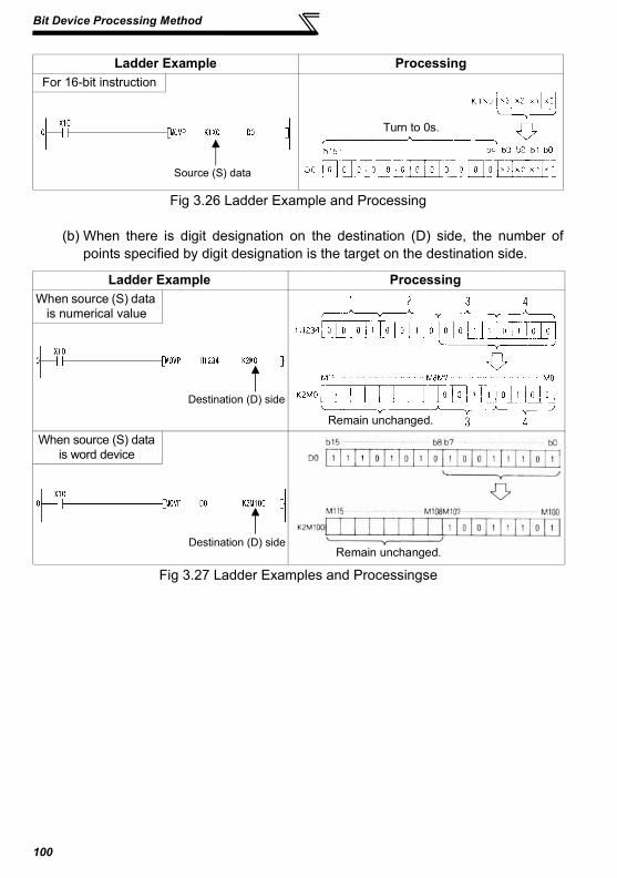
Bit Device Processing Method
100
Fig 3.26 Ladder Example and Processing
(b) When there is digit designation on the destination (D) side, the number ofpoints specified by digit designation is the target on the destination side.
Fig 3.27 Ladder Examples and Processingse
Ladder Example ProcessingFor 16-bit instruction
Ladder Example ProcessingWhen source (S) data
is numerical value
When source (S) data is word device
Turn to 0s.
Source (S) data
Remain unchanged.
Destination (D) side
Remain unchanged.Destination (D) side

101
Handling of Numerical Value
3
SEQ
UEN
CE
PRO
GR
AM
MIN
G
3.21 Handling of Numerical ValueThe built-in PLC function has instructions that handle numerical values indicated in 16bits.The most significant bit of the 16 bits is used to judge whether the value is positive ornegative. Therefore, the numerical values that can be handled as 16 bits are asfollows.
16 bits: -32768 to 32767
The decimal notation and hexadecimal notation correspond as indicated below.
POINT•Numerical value setting method1) Decimal number
2) Hexadecimal number
Decimal Notation Hexadecimal Notation32767 H7FFF
to to5 H00054 H00043 H00032 H00021 H00010 H0000-1 HFFFF-2 HFFFE-3 HFFFD-4 HFFFC-5 HFFFBto to
-32768 H8000
10 is stored into D10 in BIN.
-10 is stored into D10 in BIN.
10 is stored into D10 in hexadecimal.

102
Operation Error
3.22 Operation ErrorWhen a basic instruction is used, an operation error will occur in the followingcase.(a) If any error described in the description of the corresponding instruction
occurs.
(1) Error processingIf an operation error occurred at execution of a basic instruction, the error flagturns on and the error step number is stored into the error step storage register.
1)D9011 stores the step number of the instruction where an operation error occurredwhen M9011 turned from OFF to ON. Therefore, D9011 data does not change ifM9011 remains on.
2)To reset M9011 and D9011, program as shown below.
Fig 3.28 Special Relay and Register Resetting Ladder3)Whether sequence processing will be stopped or continued at occurrence of an
operation error can be selected by built-in PLC function parameter setting. Refer topage 94 for details.
POINTNote that if the device designation range is outside the corresponding devicerange, an operation error does not occur and data is written to other than thespecified device.
Error flagM9010 ... Turns on at an operation error and turns off if the next basic
instruction is normal.M9011.... Turns on at the first operation error.
Error step storage register
D9010.... Stores the first step number of the instruction where an operation error occurred.
D9011 .... Stores the first step number of the instruction where an operation error occurred first.
M50 to M65 are the targets, but actual setting range is M0 to M63, and error occurs since M64 and M65 do not exist.
Resets (turns off) M9011.
Resets D9011.(Clears D9011 to 0.)
Reset command
Reset command

Instructions List
SEQ
UEN
CE
PRO
GR
AM
MIN
G
103
3
3.23 Instructions List3.23.1 How to use the instruction list
1).......Classifies the instruction by application.2)....... Indicates the instruction symbol used for programming.
The instructions are based on 16-bit data instructions.Example MOV
↓16-bit transfer instruction
• Add P to the end of the instruction to define it as executed only on theleading edge of the preceding condition.Example MOV MOVP
↓ ↓Instruction executed continuously Instruction executed only on leading
while preceding condition is on edge of preceding contact condition
3)....... Indicates the symbol used in the ladder diagram.
Destination:..............................................Indicates the destination of theoperation result.
Source: ....................................................Indicates the source of the data forthe operation.
Classification Instruction Symbol Symbol Processing Execution
ConditionNumber of Steps
Transfer (S) → (D) 5
↑1)
↑2)
↑3)
↑4)
↑5)
↑6)
MOV DSMOV
MOVP DSMOVP
MOV S D
Indicates destination.
Indicates source.Indicates instruction symbol.
WAND S1 DS2
Indicates destination.
Indicates source.Indicates instruction symbol.
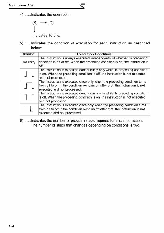
Instructions List
104
4) .......Indicates the operation.
5) .......Indicates the condition of execution for each instruction as describedbelow:
6) .......Indicates the number of program steps required for each instruction. The number of steps that changes depending on conditions is two.
Symbol Execution Condition
No entryThe instruction is always executed independently of whether its preceding condition is on or off. When the preceding condition is off, the instruction is off.The instruction is executed continuously only while its preceding condition is on. When the preceding condition is off, the instruction is not executed and not processed.The instruction is executed once only when the preceding condition turns from off to on. If the condition remains on after that, the instruction is not executed and not processed.The instruction is executed continuously only while its preceding condition is off. When the preceding condition is on, the instruction is not executed and not processed.The instruction is executed once only when the preceding condition turns from on to off. If the condition remains off after that, the instruction is not executed and not processed.
(S)
Indicates 16 bits.
(D)
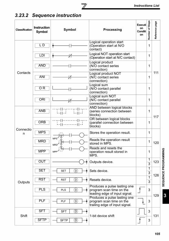
Instructions List
SEQ
UEN
CE
PRO
GR
AM
MIN
G
105
3
3.23.2 Sequence instruction
ClassificationInstruction
Symbol Symbol ProcessingExecuti
on Conditi
on
Num
ber o
f Ste
ps
Ref
eren
ce p
age
Contacts
Logical operation start (Operation start at N/O contact)
1
111
Logical NOT operation start (Operation start at N/C contact) 1
Logical product (N/O contact series connection)
1
Logical product NOT (N/C contact series connection)
1
Logical sum (N/O contact parallel connection)
1
Logical sum NOT (N/C contact parallel connection)
1
Connection
AND between logical blocks (series connection between blocks)
1117OR between logical blocks
(parallel connection between blocks)
1
Stores the operation result. 1
120Reads the operation result stored in MPS. 1
Reads and resets the operation result stored in MPS.
1
Outputs
Outputs device.1
1233
Sets device.1
1263
Resets device.13
Produces a pulse lasting one program scan time on the leading edge of input signal.
3129Produces a pulse lasting one
program scan time on the trailing edge of input signal.
3
Shift 1-bit device shift3
1313
L D
LDI
AND
ANI
O R
ORI
ANB
ORB
MPS
MPS
MRD
MPP
MRD
MPP
OUT
SET SET D
RST RST D
PLS PLS D
PLF PLF D
SFT SFT D
SFTP SFTP D

Instructions List
106
Master control
Master control start 5133
Master control reset 3
Program end —
Must be written at the end of sequence program to return to step 0.
1 137
No operation
— No operationFor program deletion or space 1 138
—No operationLine feed instruction for printer output
1 -
ClassificationInstruction
Symbol Symbol ProcessingExecuti
on Conditi
on
Num
ber o
f Ste
ps
Ref
eren
ce p
age
M C MC Dn
MCR MCR n
END
NOP
NOPLF
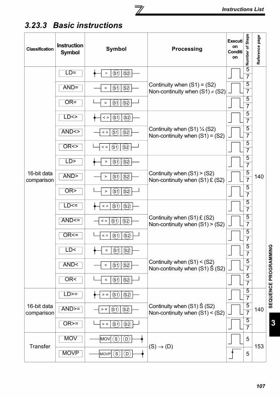
Instructions List
SEQ
UEN
CE
PRO
GR
AM
MIN
G
107
3
3.23.3 Basic instructions
ClassificationInstruction
Symbol Symbol ProcessingExecuti
on Conditi
on
Num
ber o
f Ste
ps
Ref
eren
ce p
age
16-bit datacomparison
Continuity when (S1) = (S2)Non-continuity when (S1) ≠ (S2)
5
140
75757
Continuity when (S1) ¼ (S2)Non-continuity when (S1) = (S2)
575757
Continuity when (S1) > (S2)Non-continuity when (S1) £ (S2)
575757
Continuity when (S1) £ (S2)Non-continuity when (S1) > (S2)
575757
Continuity when (S1) < (S2)Non-continuity when (S1) Š (S2)
575757
16-bit data comparison
Continuity when (S1) Š (S2)Non-continuity when (S1) < (S2)
5
140
75757
Transfer (S) → (D)5
1535
LD= S1 S2=
AND= S1 S2=
OR= S1 S2=
LD<> S1 S2< >
AND<> S1 S2< >
OR<> S1 S2< >
LD> S1 S2>
AND> S1 S2>
OR> S1 S2>
LD<= S1 S2< =
AND<= S1 S2< =
OR<= S1 S2< =
LD< S1 S2<
AND< S1 S2<
OR< S1 S2<
LD>= S1 S2> =
AND>= S1 S2> =
OR>= S1 S2> =
MOV DSMOV
MOVP DSMOVP
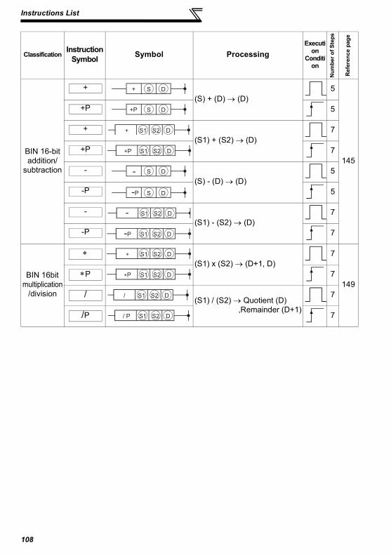
Instructions List
108
BIN 16-bit addition/
subtraction
(S) + (D) → (D)5
145
5
(S1) + (S2) → (D)7
7
(S) - (D) → (D)5
5
(S1) - (S2) → (D)7
7
BIN 16bit multiplication
/division
(S1) x (S2) → (D+1, D)7
1497
(S1) / (S2) → Quotient (D) ,Remainder (D+1)
7
7
ClassificationInstruction
Symbol Symbol ProcessingExecuti
on Conditi
on
Num
ber o
f Ste
ps
Ref
eren
ce p
age
+ DS+
+P DS+P
+ + DS2S1
+P +P DS2S1
- DS-
-P DS-P
- - DS2S1
-P -P DS2S1
∗ ∗ DS2S1
∗P ∗P DS2S1
/ / DS2S1
/P / P DS2S1

Instructions List
SEQ
UEN
CE
PRO
GR
AM
MIN
G
109
3
3.23.4 Application instructions
ClassificationInstruction
Symbol Symbol ProcessingExecuti
on Conditi
on
Num
ber o
f Ste
ps
Ref
eren
ce p
age
Logical product
(D) AND (S) → (D)5
1565
(S1) AND (S2) → (D)7
7
Logical sum
(D) OR (S) → (D)5
1595
(S1) OR (S2) → (D)7
7
Exclusive logical sum
(D) XOR (S) → (D)5
1625
(S1) XOR (S2) → (D)7
7
NOT exclusive
logical sum
(D) XOR (S) → (D)5
1655
(S1) XOR (S2) → (D)7
7
2’s complement 0 - (D) → (D)
3168
3
WAND DSWAND
WANDP WANDP DS
WAND WAND DS2S1
WANDP WANDP DS2S1
WOR DSWOR
WORP WORP DS
WOR WOR DS2S1
WORP WORP DS2S1
WXOR DSWXOR
WXORP DSWXORP
WXOR WXOR DS2S1
WXORP WXORP DS2S1
WXNR DSWXNR
WXNRP DSWXNRP
WXNR WXNR DS2S1
WXNRP WXNRP DS2S1
NEG DNEG
NEGP DNEGP

110
Description of the Instructions
3.24 Description of the InstructionsIn Chapter 6, the instructions are described in the following format.
Description1) Indicates the section number, instruction outlines and instruction symbols.2)The devices usable with the instructions are marked.3)The digit designation that can be set is indicated for the instruction that requires digit
designation when a bit device is used.4)The instruction for which the error flag turns on at operation error occurrence is
marked.5)Shows the format in the ladder mode.6)Explains the instruction.7) Indicates the execution conditions of the instructions.8)Shows program examples in the ladder mode and list mode.
Output Instructions
6.5.2 Device set, reset ... SET, RST
Functions
(1) Turns on the specified device when the SET input turns on.(2) The device turned on is held on if the SET input turns off. It can be turned off by
the RST instruction.
(3) When the SET input is off, the device status does not change.
Execution ConditionsThe SET and RST instructions are executed every scan.
Program Examples
, 1)Program that sets (turns on) Y8 when X8 turns on and resets (turns off) Y8 when X9
turns on.
Usable Devices
Digit Designation
Error FlagBit devices
Word (16-bit) devices
Constants Level
X Y M T C D K H N(M9010,M9011)
SET � �
RST � � � � �
SET
D
SET input
RST inputSET
Device number to be set (turned on)
RST Device number to be reset
D
SET input
RST input
SET RST
Coding
3) 4)1)
2)
5)
6)
7)
8)

Sequence Instructions
SEQ
UEN
CE
PRO
GR
AM
MIN
G
111
3
3.25 Sequence Instructions
Sequence instructions are used for relay control circuits, etc.
3.25.1 Contact Instructions : Operation start, series connection, parallel connection ... LD, LDI, AND, ANI, OR, ORI
Usable Devices Digit Designation
Error FlagBit devices Word (16-bit) devices Constants Level
X Y M T C D K H N (M9010,M9011)
Device numberX1
X1
X2
X2
X3
X3
LD
LDI
AND
ANI
OR
ORI
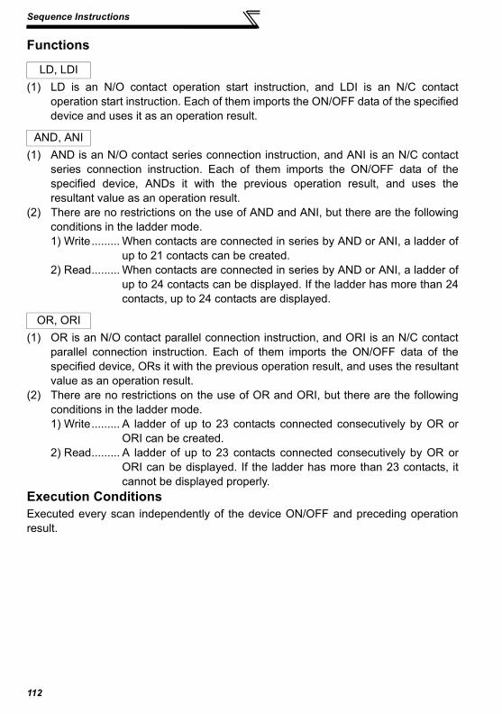
Sequence Instructions
112
Functions
(1) LD is an N/O contact operation start instruction, and LDI is an N/C contactoperation start instruction. Each of them imports the ON/OFF data of the specifieddevice and uses it as an operation result.
(1) AND is an N/O contact series connection instruction, and ANI is an N/C contactseries connection instruction. Each of them imports the ON/OFF data of thespecified device, ANDs it with the previous operation result, and uses theresultant value as an operation result.
(2) There are no restrictions on the use of AND and ANI, but there are the followingconditions in the ladder mode.1) Write......... When contacts are connected in series by AND or ANI, a ladder of
up to 21 contacts can be created.2) Read......... When contacts are connected in series by AND or ANI, a ladder of
up to 24 contacts can be displayed. If the ladder has more than 24contacts, up to 24 contacts are displayed.
(1) OR is an N/O contact parallel connection instruction, and ORI is an N/C contactparallel connection instruction. Each of them imports the ON/OFF data of thespecified device, ORs it with the previous operation result, and uses the resultantvalue as an operation result.
(2) There are no restrictions on the use of OR and ORI, but there are the followingconditions in the ladder mode.1) Write......... A ladder of up to 23 contacts connected consecutively by OR or
ORI can be created.2) Read......... A ladder of up to 23 contacts connected consecutively by OR or
ORI can be displayed. If the ladder has more than 23 contacts, itcannot be displayed properly.
Execution ConditionsExecuted every scan independently of the device ON/OFF and preceding operationresult.
LD, LDI
AND, ANI
OR, ORI

Sequence Instructions
SEQ
UEN
CE
PRO
GR
AM
MIN
G
113
3
Program Examples , , , , ,
3.25.2 Contact Instructions : Ladder block series connection, parallel connection ... ANB, ORB
Usable Devices Digit Designation
Error FlagBit devices Word (16-bit) devices Constants Level
X Y M T C D K H N (M9010,M9011)
LD LDI AND ANI OR ORI
ORB
ANB
Coding・
Coding・
Coding・

Sequence Instructions
114
Block A Block B
Use OR or ORI to connectcontacts in parallel.
Block A
Block B

Sequence Instructions
SEQ
UEN
CE
PRO
GR
AM
MIN
G
115
3
Functions
(1) ANDs blocks A and B and uses the resultant value as an operation result.(2) The symbol of ANB is not a contact symbol but a connection symbol.(3) ANB can be written up to seven instructions (eight blocks) consecutively.
If ANB is written consecutively more than the above, the PLC cannot performnormal operation.
(1) ORs blocks A and B and uses the resultant value as an operation result.(2) ORB connects in parallel the ladder blocks of two or more contacts. Use OR or
ORI to connect in parallel the ladder blocks of only one contact.
(3) The symbol of ORB is not a contact symbol but a connection symbol.(4) ORB can be written up to seven instructions (eight blocks) consecutively.
If ORB is written consecutively more than the above, the PLC cannot performnormal operation.
ANB
ORB
Coding

Sequence Instructions
116
Program Examples
Though there are the following two different program coding methods for connectingladder blocks in series consecutively, use the coding example 1.
Though there are the following two different program coding methods for connectingladder blocks in parallel consecutively, use the coding example 1.
ANB
Coding example 1 Coding example 2
ORB
Coding example 1 Coding example 2
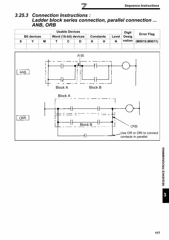
Sequence Instructions
SEQ
UEN
CE
PRO
GR
AM
MIN
G
117
3
3.25.3 Connection Instructions : Ladder block series connection, parallel connection ... ANB, ORB
Usable Devices Digit Designation
Error FlagBit devices Word (16-bit) devices Constants Level
X Y M T C D K H N (M9010,M9011)
Block A Block B
Use OR or ORI to connectcontacts in parallel.
Block A
Block B

Sequence Instructions
118
Functions
(1) ANDs blocks A and B and uses the resultant value as an operation result.(2) The symbol of ANB is not a contact symbol but a connection symbol.(3) ANB can be written up to seven instructions (eight blocks) consecutively.
If ANB is written consecutively more than the above, the PLC cannot performnormal operation.
(1) ORs blocks A and B and uses the resultant value as an operation result.(2) ORB connects in parallel the ladder blocks of two or more contacts. Use OR or
ORI to connect in parallel the ladder blocks of only one contact.
(3) The symbol of ORB is not a contact symbol but a connection symbol.(4) ORB can be written up to seven instructions (eight blocks) consecutively.
If ORB is written consecutively more than the above, the PLC cannot performnormal operation.
ANB
ORB
Coding

Sequence Instructions
SEQ
UEN
CE
PRO
GR
AM
MIN
G
119
3
Program Examples
Though there are the following two different program coding methods for connectingladder blocks in series consecutively, use the coding example 1.
Though there are the following two different program coding methods for connectingladder blocks in parallel consecutively, use the coding example 1.
ANB
Coding example 1 Coding example 2
ORB
Coding example 1 Coding example 2

Sequence Instructions
120
3.25.4 Connection Instructions : Operation result, push, read, pop ... MPS, MRD, MPP
Functions
(1) Stores the operation result (ON/OFF) immediately before itself.(2) The MPS instruction can be used consecutively up to 12 times.
In the ladder mode, however, it can be used up to 11 times.When the MPP instruction is used midway, the number of used MPS instructionsis decremented by 1.
(1) Reads the operation result stored by the MPS instruction, and continuesoperation from the next step with that operation result.
(1) Reads the operation result stored by the MPS instruction, and continuesoperation from the next step with that operation result.
(2) Clears the operation result stored by the MPS instruction.
Usable Devices Digit Designation
Error FlagBit devices Word (16-bit) devices Constants Level
X Y M T C D K H N (M9010,M9011)
MPS
MRD
MPP
MPS, MRD and MPP do not appear in ladder display.

Sequence Instructions
SEQ
UEN
CE
PRO
GR
AM
MIN
G
121
3
POINT(1) Ladders differ as shown below between when MPS, MRD and MPP are used and when they
are not used.
(2) Use the same number of MPS and MPP instructions. If they differ in the number of used instructions, operation will be performed as described below.1) If the MPS instructions are used more than MPP instructions, the ladder is changed and
the built-in PLC function performs operation according to the new ladder.
2) If the MPP instructions are used more than MPS instructions, that ladder block results in a ladder creation error, and the built-in PLC function cannot perform normal operation.
Ladder using MPS, MRD and MPP Ladder not using MPS, MRD and MPP
Coding
Coding
When MPP is replaced by NOP
Before change
After change
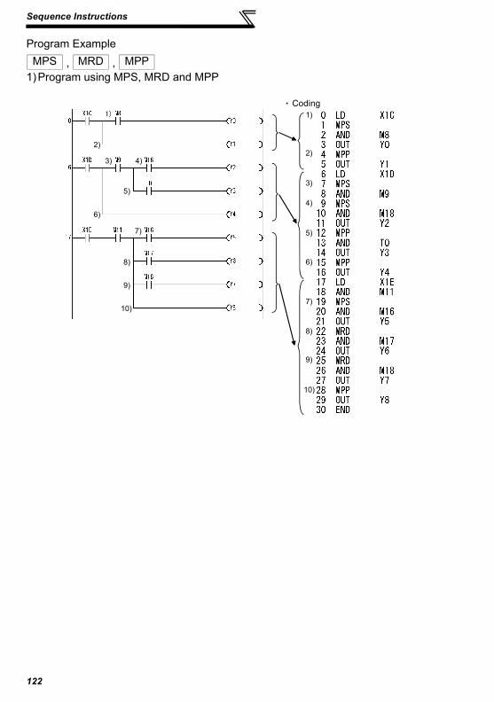
Sequence Instructions
122
Program Example
, , 1)Program using MPS, MRD and MPP
MPS MRD MPP
1)
2)
3) 4)
5)
6)
7)
8)
9)
10)
1)
2)
3)
4)
5)
6)
7)
8)
9)
10)
Coding・
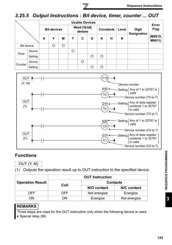
Sequence Instructions
SEQ
UEN
CE
PRO
GR
AM
MIN
G
123
3
3.25.5 Output Instructions : Bit device, timer, counter ... OUT
Functions
(1) Outputs the operation result up to OUT instruction to the specified device.
Usable Devices
DigitDesignation
Error FlagBit devices Word (16-bit)
devices Constants Level
X Y M T C D K H N (M9010, M9011)
Bit device
TimerDevice
Setting
CounterDevice
Setting
OUT (Y, M)
Operation ResultOUT Instruction
CoilContacts
N/O contact N/C contactOFF OFF Not energize EnergizeON ON Energize Not energize
REMARKSThree steps are used for the OUT instruction only when the following device is used.• Special relay (M)
T0
T0
C0
C1
OUT Y15
Device numberK50
Device number (T0 to 7)
D10
K50
Device number (C0 to 7)
OUT
OUT
Device number (T0 to 7)
Device number (C0 to 7)
(Y, M)
(T)
(C)D10
Setting Any of data register contents 1 to 32767 is valid
Setting Any of 1 to 32767 is valid
Setting Any of 1 to 32767 is valid
Setting Any of data register contents 1 to 32767 is valid

Sequence Instructions
124
(1) When the operation result up to the OUT instruction is ON, the coil of the timerturns on and the timer times up to the setting, and when the timer times out(timing value ≥ setting), the contact operates as indicated below.
(2) When the operation result up to the OUT instruction turns from ON to OFF, thetimer operates as indicated below.
(3) After a time-out, the contact state of the retentive timer remains unchanged untilthe RST instruction is executed.
(4) A negative number (-32768 to -1) cannot be specified for the setting.(5) If the setting is 0, it is timed as infinity. Hence, the timer does not time out.(6) Refer to page 81 for the timing method of the timer.
(1) When the operation result up to the OUT instruction turns from OFF to ON, thepresent value (count value) is incremented by 1, and when the counter stopscounting (present value = setting), the contact operates as indicated below.
(2) The counter does not count if the operation result remains ON. (Count inputsneed not be converted into pulses.)
(3) After the counter has stopped counting, the count value and contact state remainunchanged until the RST instruction is executed.
(4) A negative number (-32768 to -1) cannot be specified for the setting. If the settingis 0, processing is the same as when the setting is 1.
(5) Refer to page 83 for the counting method of the counter.
Execution ConditionsExecuted every scan independently of the operation result up to the OUT instruction.
OUT(T)
N/O contact EnergizeN/C contact Not energize
Timer Type Timer Coil
Present Value of
Timer
Before Time-out After Time-outN/O
contactN/C
contactN/O
contactN/C
contact100ms timer
OFF 0 Not energize Energize Not
energize Energize10ms timer100ms retentive timer OFF Maintained Not
energize Energize Energize Not energize
OUT(C)
N/O contact EnergizeN/C contact Not energize
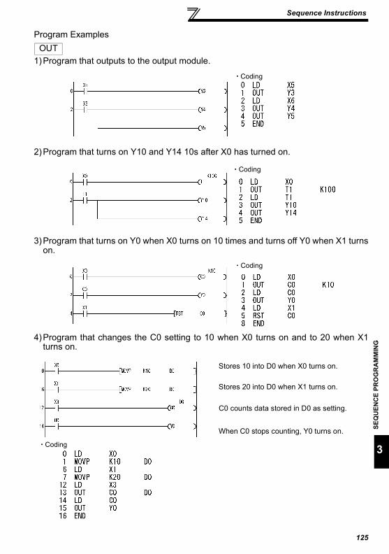
Sequence Instructions
SEQ
UEN
CE
PRO
GR
AM
MIN
G
125
3
Program Examples
1)Program that outputs to the output module.
2)Program that turns on Y10 and Y14 10s after X0 has turned on.
3)Program that turns on Y0 when X0 turns on 10 times and turns off Y0 when X1 turnson.
4)Program that changes the C0 setting to 10 when X0 turns on and to 20 when X1turns on.
OUT
Coding
Coding
Coding
Stores 10 into D0 when X0 turns on.
Stores 20 into D0 when X1 turns on.
C0 counts data stored in D0 as setting.
When C0 stops counting, Y0 turns on.
Coding
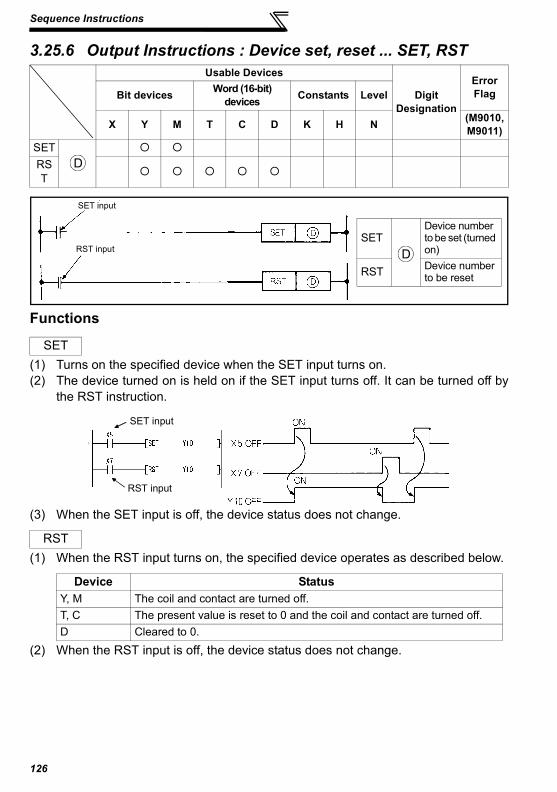
Sequence Instructions
126
3.25.6 Output Instructions : Device set, reset ... SET, RST
Functions
(1) Turns on the specified device when the SET input turns on.(2) The device turned on is held on if the SET input turns off. It can be turned off by
the RST instruction.
(3) When the SET input is off, the device status does not change.
(1) When the RST input turns on, the specified device operates as described below.
(2) When the RST input is off, the device status does not change.
Usable Devices
Digit Designation
Error FlagBit devices Word (16-bit)
devices Constants Level
X Y M T C D K H N (M9010,M9011)
SETRST
SET
RST
Device StatusY, M The coil and contact are turned off.T, C The present value is reset to 0 and the coil and contact are turned off.D Cleared to 0.
D
SET input
RST inputSET
Device number to be set (turned on)
RST Device number to be reset
D
SET input
RST input

Sequence Instructions
SEQ
UEN
CE
PRO
GR
AM
MIN
G
127
3
(3) The function of RST (D) is the same as that of the following ladder.
Execution ConditionsThe SET and RST instructions are executed every scan.
Program Examples ,
1)Program that sets (turns on) Y8 when X8 turns on and resets (turns off) Y8 when X9turns on.
Operations of SET and RST instructions
REMARKSThree steps are used when the following device is used.SET instruction ... Special relay (M)RST instruction ... Special relay (M), all word devices
RST input RST input
Device number(D)
Device number(D)
SET RST
Coding
X8 (SET input)
X9 (RST input)
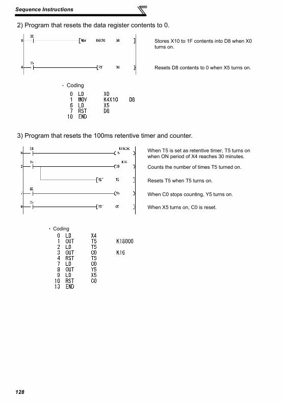
Sequence Instructions
128
2) Program that resets the data register contents to 0.
3) Program that resets the 100ms retentive timer and counter.
Stores X10 to 1F contents into D8 when X0 turns on.
Resets D8 contents to 0 when X5 turns on.
Coding
When T5 is set as retentive timer, T5 turns on when ON period of X4 reaches 30 minutes.
Counts the number of times T5 turned on.
Resets T5 when T5 turns on.
When C0 stops counting, Y5 turns on.
When X5 turns on, C0 is reset.
・ Coding

Sequence Instructions
SEQ
UEN
CE
PRO
GR
AM
MIN
G
129
3
3.25.7 Output Instructions : Leading edge, trailing edge differential outputs ... PLS, PLF
Functions
(1) Turns the specified device on when the PLS command turns from OFF to ON,and turns it off except when the PLS command turns from OFF to ON.
When there is one PLS instruction for the device specified at during one scan,the specified device turns on for one scan.Do not execute the PLS instruction for the same device more than once duringone scan.
(2) If the status is switched to STOP and switched to RUN again after execution ofthe PLS instruction, the PLS instruction is not executed.
Usable DevicesDigit
Designation
Error FlagBit devices Word (16-bit) devices Constants Level
X Y M T C D K H N (M9010, M9011)
PLS
D
PLS command
PLF command
Set data
Device number whose data will be converted into pulsesD
D
1 scan 1 scan

Sequence Instructions
130
(1) Turns the specified device on one scan when the PLF command turns from ON toOFF, and turns it off except when the PLF command turns from ON to OFF.When there is one PLF instruction for the device specified at during one scan,the specified device turns on for one scan.Do not execute the PLF instruction for the same device more than once duringone scan.
(2) If the status is switched to STOP and switched to RUN again after execution ofthe PLF instruction, the PLF instruction is not executed.
Program Examples
Program that executes the PLS instruction when X9 turns on.
Program that executes the PLF instruction when X9 turns off.
PLF
D
1 scan 1 scan
PLS
・ Coding
1 scan
PLF
・ Coding
1 scan

Sequence Instructions
SEQ
UEN
CE
PRO
GR
AM
MIN
G
131
3
3.25.8 Shift Instructions : Bit device shift ... SFT, SFTP
Functions
(1) Shifts the ON/OFF status of the device preceding the one specified at to thespecified device, and turns off the preceding device.
(2) Use the SET instruction to turn on the first device from which data will be shifted.(3) When using the SFT or SFTP instructions consecutively, program in order of
larger to smaller device numbers.
Usable DevicesDigit
Designation
Error FlagBit devices Word (16-bit) devices Constants Level
X Y M T C D K H N (M9010,M9011)
D
SFT commandsSet data
Device number to which data will be shiftedD
D
X02 ON
After first shift input
After second shift input
X02 ON
After third shift input
After fourth shift input
After fifth shift input
*At M8 to 15, 1 indicates ON and 0 indicates OFF.
Shift input
5)
6)
7)
Shift range
1)
2)
3)
4)
5)
6)
7)
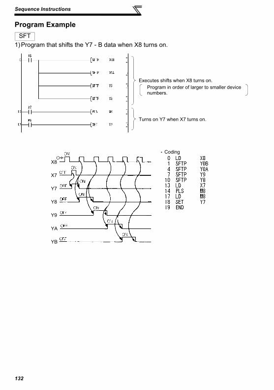
Sequence Instructions
132
Program Example
1)Program that shifts the Y7 - B data when X8 turns on.SFT
Executes shifts when X8 turns on.Program in order of larger to smaller device numbers.
Turns on Y7 when X7 turns on.
X8
X7
Y7
Y8
Y9
YA
YB
Coding

Sequence Instructions
SEQ
UEN
CE
PRO
GR
AM
MIN
G
133
3
3.25.9 Master Control Instructions : Master control set, reset ... MC, MCR
Functions(1) The master control instructions are designed to create an efficient ladder
switching sequence program by switching on/off the common bus of the ladder.The ladder that uses master control is as shown below.
Usable DevicesDigit
Designation
Error FlagBit devices Word (16-bit) devices Constants Level
X Y M T C D K H N (M9010, M9011)
n
D
MC ON/OFF command
Nesting (N0 to 7)
Device
Set data
n Nesting (N0 to 7)Device number to be turned onD
Y7
YF
Y10
Display in ladder mode of GPP
Executed only when X0 is on
Actual operation ladder

Sequence Instructions
134
(1) When the MC ON/OFF command is on at the start of master control, theoperation results between MC and MCR are as performed by the instructions(ladder).
(2) If the MC instruction is off, the scan between the MC and MCR instructions isexecuted, and therefore, the scan time does not become short.When the MC instruction is off, the operation results between MC and MCR areas described below.
(3) By changing the device at , the MC instruction can use the same nesting (N)number any number of times.
(4) When the MC instruction is on, the coil of the device specified at turns on.Since using the same device in the OUT instruction, etc. will result in double coils,
the device specified at should not be used in any other instruction.
MC
100ms, 10ms timer The count value is reset to 0 and both the coil and contact turn off.
100ms retentive timer, counter The coil turns off but both the count value and contact maintain the current states.
Devices in OUT instruction All turn off.SET, RST, SFT or basic
device in instruction Maintains the current state.
D
D
D

Sequence Instructions
SEQ
UEN
CE
PRO
GR
AM
MIN
G
135
3
(1) This instruction is designed to reset the master control and indicates the end of themaster control range.
(2) Do not provide a contact instruction in front of the MCR instruction.The master control instructions can be nested. Their master control ranges aredifferentiated by the nesting (N). The nesting can be used from N0 to N7.Using the nesting structure, you can create a ladder that restricts the programexecution conditions in order.The ladder using the nesting structure is as shown below.
MCR
A
B
C
‰ñ H̃ �ƒ‚ [ ƒh ‚Å ‚Ì •\ Ž¦Display in ladder mode Actual operation ladder
Executed when A turns on.
Executed when A and B turn on.
Executed when A, B and C turn on.
Executed when A and B turn on.
Executed when A turns on.
Irrelevant to A, B and C.

Sequence Instructions
136
Note the following when nesting the instructions.(1) The instructions can be nested to a level of eight (N0 to 7). When nesting them,
use MC from lower to higher nesting (N) numbers and MCR from higher to lowernumbers. In the opposite order, the PLC function cannot perform normaloperation since the instructions cannot be nested.
(2) When the MCR instructions are gathered in one place in the nesting structure, allmaster controls can be terminated by one lowest nesting (N) number.
Since buses cross each other, normal master control ladder cannot be created.
A
B
Display in ladder mode
Nesting numbers of MCR are opposite.
Actual operation ladder
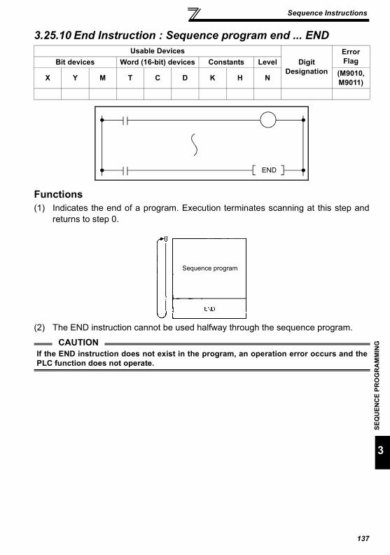
137
Sequence Instructions
3
SEQ
UEN
CE
PRO
GR
AM
MIN
G
3.25.10 End Instruction : Sequence program end ... END
Functions(1) Indicates the end of a program. Execution terminates scanning at this step and
returns to step 0.
(2) The END instruction cannot be used halfway through the sequence program.
Usable DevicesDigit
Designation
Error FlagBit devices Word (16-bit) devices Constants Level
X Y M T C D K H N (M9010, M9011)
CAUTIONIf the END instruction does not exist in the program, an operation error occurs and thePLC function does not operate.
END
Sequence program

Sequence Instructions
138
3.25.11 Other Instructions : No operation ... NOP
Functions
(1) No-operation instruction that has no influence on the preceding operation.(2) Use NOP to:
1) Provide space for debugging of a sequence program.2) Delete an instruction without changing the number of steps. (Change the
instruction for NOP)3) Delete an instruction temporarily.
Usable DevicesDigit
Designation
Error FlagBit devices Word (16-bit) devices Constants Level
X Y M T C D K H N (M9010, M9011)
NOP
NOP does not appear in ladder display.

Sequence Instructions
SEQ
UEN
CE
PRO
GR
AM
MIN
G
139
3
Program Examples
1) Contact short-circuit (AND, ANI)
2) Contact short-circuit (LD, LDI).......Note that if LD or LDI is replaced by NOP, theladder will be completely changed.
NOP
Before change
Replaced by NOP.
After change
Coding
Coding
Replaced by LD T3.
Before change
Replaced by NOP.
After change
Coding
Replaced by NOP.
Before change
After change
Coding

Basic Instructions
140
3.26 Basic Instructions
The basic instructions can handle numerical data represented in 16 bits.
3.26.1 Comparison Operation Instructions(1) The comparison operation instruction is handled as a contact, compares the
magnitudes of two pieces of data (e.g. =, >, <), and turns on when the conditionholds.
(2) Use the comparison operation instructions in the same manner as the contactinstructions of the PLC instructions as indicated below.• LD, LDI ......... LD=• AND, ANI ..... AND=• OR, ORI ....... OR=
(3) There are the following 18 different comparison operation instructions.Refer to page 142 for details.
(4) The conditions that the comparison operation instructions turn on are as follows.
Classification Instruction Symbol Classification Instruction
Symbol Classification Instruction Symbol
=LD=
>LD>
<LD<
AND= AND> AND<OR= OR> OR<
≠
LD<>≤
LD<=≥
LD>=AND<> AND<= AND>=OR<> OR<= OR>=
ONOFF OFFDn = K100
98 99 100 101 102
OFF ONDn K100
OFFONDn K100
OFFON ONDn K100
ON OFFDn K100
OFF ONDn K100

Basic Instructions
SEQ
UEN
CE
PRO
GR
AM
MIN
G
141
3
CAUTIONThe comparison instruction regards the specified data as BIN values. Hence, if the valuewhose most significant bit (b15) is 1 (8 to F) is specified for comparison of hexadecimaldata, it is regarded as a negative BIN value.
Comparison of 4-digit HEX values
Therefore, the result is -32767 < 1384 and Y10 does not turn on.
Example
Regarded as -32767 in BIN.
Regarded as 1384 in BIN.

Basic Instructions
142
3.26.2 Comparison Operation Instructions : 16-bit data comparison ... =, <>, >, <=, <, >=
Functions(1) Handled as an N/O contact and performs 16-bit comparison operation.(2) The comparison operation results are as indicated below.
Execution ConditionsThe execution conditions of LD , AND and OR are as indicated below.
Usable DevicesDigit
Designation
Error FlagBit devices Word (16-bit) devices Constants Level
X Y M T C D K H N (M9010, M9011)
K1 to K4
Instruction symbol in Condition
Comparison Operation
Result
Instruction symbol in Condition
Comparison Operation
Result= =
Energize
= ≠
Not energize
<> ≠ <> =
> > > ≤
<= ≤ <= >
< < < ≥
>= ≥ >= <
Instruction Execution ConditionLD Executed every scan.
AND Executed only when the preceding contact instruction is on.
OR Executed every scan.
S1
S2
Instruction symbol in =, <>, >, <=, <, >=
Compared data or head numbers of devices that store compared data
S1
S2
S1 S2 S1 S2S1 S2 S1 S2S1 S2 S1 S2S1 S2 S1 S2S1 S2 S1 S2S1 S2 S1 S2
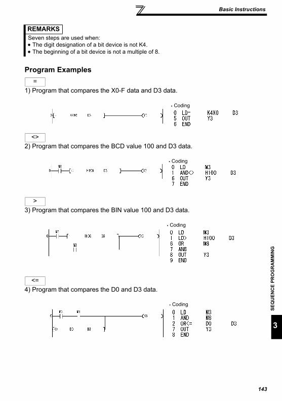
Basic Instructions
SEQ
UEN
CE
PRO
GR
AM
MIN
G
143
3
Program Examples
1) Program that compares the X0-F data and D3 data.
2) Program that compares the BCD value 100 and D3 data.
3) Program that compares the BIN value 100 and D3 data.
4) Program that compares the D0 and D3 data.
REMARKSSeven steps are used when:• The digit designation of a bit device is not K4.• The beginning of a bit device is not a multiple of 8.
=
Coding
<>
Coding
>
Coding
<=
Coding

Basic Instructions
144
3.26.3 Arithmetic Operation InstructionsThe arithmetic operation instructions are instructions which perform the addition,subtraction, multiplication, and division of two BIN data.
(1) Arithmetic operation with BIN (Binary)• If the operation result of an addition instruction exceeds 32767 , the result
becomes a negative value.• If the operation result of a subtraction instruction is less than - 32768 , the result
becomes a positive value.• The operation of a positive value and a negative value is as follows:
5 + 8 →13 5 - 8 → -3 5 x 3 → 15-5 x 3 → -15-5 x (-3) → 15-5 / 3 → -1 and remainder -2 5 / (-3) → -1 and remainder 2-5 / (-3) → 1 and remainder -2

Basic Instructions
SEQ
UEN
CE
PRO
GR
AM
MIN
G
145
3
3.26.4 Arithmetic Operation Instructions : BIN 16-bit addition, subtraction ... +, +P, -, -P
Usable Devices
Digit Designation
Error FlagBit devices Word (16-bit)
devices Constants Level
X Y M T C D K H N (M9010, M9011)
K1 to K4
S
D
S1
S2
D1
Addition/subtraction commands
Addition/subtraction commands
Instruction symbol in
Setting data
+, -
Addend/subtrahend or head device number storing addend/subtrahendHead device number storing augend/minuendAugend/minuend or head device number storing augend/ minuendAddend/subtrahend or head device number storing addend/subtrahendHead device number which will store the operation result
S
D
S1
S2
D1
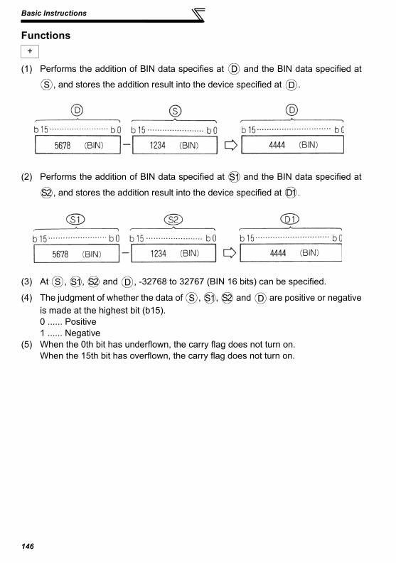
Basic Instructions
146
Functions
(1) Performs the addition of BIN data specifies at and the BIN data specified at
, and stores the addition result into the device specified at .
(2) Performs the addition of BIN data specified at and the BIN data specified at
, and stores the addition result into the device specified at .
(3) At , , and , -32768 to 32767 (BIN 16 bits) can be specified.
(4) The judgment of whether the data of , , and are positive or negativeis made at the highest bit (b15).0 ...... Positive1 ...... Negative
(5) When the 0th bit has underflown, the carry flag does not turn on.When the 15th bit has overflown, the carry flag does not turn on.
+
D
S D
S1
S2 D1
S S1 S2 D
S S1 S2 D

Basic Instructions
SEQ
UEN
CE
PRO
GR
AM
MIN
G
147
3
Functions
(1) Performs the subtraction of BIN data specifies at and the BIN data specified
at , and stores the subtraction result into the device specified at .
(2) Performs the subtraction of BIN data specified at and the BIN data specified
at , and stores the subtraction result into the device specified at .
(3) At , , and , -32768 to 32767 (BIN 16 bits) can be specified.
(4) The judgment of whether the data of , , and are positive or negativeis made at the highest bit (b15).0 ...... Positive1 ...... Negative
(5) When the 0th bit has underflown, the carry flag does not turn on.When the 15th bit has overflown, the carry flag does not turn on.
-
D
S D
S1
S2 D1
S S1 S2 D
S S1 S2 D

Basic Instructions
148
Execution ConditionsAddition/subtraction command.
Program Examples
Program which adds the content of A0 to the content of D3 and outputs the result toY38 to 3F when X5 turns on.
Program which outputs the difference between the set value and present valuetimer T3 to Y40 to 53 in BCD.
Addition/subtraction
command
Executed everyscan.
Executed everyscan.
Executed only once. Executed only once.
+
Coding
-
Coding

Basic Instructions
SEQ
UEN
CE
PRO
GR
AM
MIN
G
149
3
3.26.5 Arithmetic Operation Instructions : BIN 16-bit multiplication, division ... *, *P, /, /P
Usable Devices
Digit Designation
Error FlagBit devices Word (16-bit)
devices Constants Level
X Y M T C D K H N (M9010, M9011)
K1 to K4
S1
S2
D
Multiplication/division commands Instruction symbol in
Setting data
∗, /
Multiplicand/dividend or head device number storing multiplier/dividendMultiplicand/divider or head device number storing multiplier/dividerHead device number which will store the result
S1
S2
D

Basic Instructions
150
Functions
(1) Performs the multiplication of BIN data specified at and the BIN data specified
at , and stores the multiplication result into the device specified at .
(2) When is a bit device, specify the bits, beginning with the lower bits.Example
K1: Lower 4 bits (b0 to 3)K4: Lower 16 bits (b0 to 15)
(3) At and , -32768 to 32767 (BIN 16 bits) can be specified.
(4) The judgment of whether the data of and are positive or negative is made
at the highest bit (b15) and that of , at (b31).0 ...... Positive1 ...... Negative
∗
S1
S2 D
D
S1 S2
S1 S2
D

Basic Instructions
SEQ
UEN
CE
PRO
GR
AM
MIN
G
151
3
(1) Performs the division of BIN data specified at and the BIN data specified at
, and stores the result into the device specified at .
(2) In regards to the operation result, the quotient and remainder are stored by use of32 bits in the case of word device, and only the quotient is stored by use of 16 bitsin the case of bit device.
Quotient : Stored to the lower 16 bits.Remainder : Stored to the upper 16 bits. (Storable only in the case of word
device)
(3) At and , -32768 to 32767 (BIN 16 bits) can be specified.
(4) The judgment of whether the data of , , and +1 are positive ornegative is made at the highest bit (b15).(Both quotient and remainder have sign.)0 ...... Positive1 ...... Negative
Execution ConditionsThe execution conditions of the transfer instructions are as shown below.
/
S1
S2 D
Quotient Remainder
S1 S2
S1 S2 D D
Multiplication/division
command
Executed every scan.
Executed every scan.
Executed only once. Executed only once.

Basic Instructions
152
Operation ErrorsIn the following case, operation error occurs and the error flag turns on.
• A1 or V has been specified at .
• The divisor is 0.
Program Examples
1)Program which stores the multiplication result of 5678 and 1234 in BIN to D3 and 4when X5 turns on.
2)Program which outputs the multiplication result of the BIN data of X8 to F and theBIN data of X10 to 1B to Y30 to 3F.
Program which outputs the quotient, obtained by dividing the data of X8 to F by 3.14,to Y30 to 3F when X3 turns on.
∗
/
D
S2

Basic Instructions
SEQ
UEN
CE
PRO
GR
AM
MIN
G
153
3
3.26.6 Data Transfer InstructionsThe data transfer instructions are designed to transfer data.The data moved by the data transfer instruction is maintained until new data is transferred.
3.26.7 Data Transfer Instructions : 16-bit data transfer ... MOV, MOVP
Functions
Transfers the 16-bit data of the device specified at to the device specified at .
Execution ConditionsThe execution conditions of the transfer instructions are as shown below.
Usable Devices
Digit Designation
Error FlagBit devices Word (16-bit)
devices Constants Level
X Y M T C D K H N (M9010, M9011)
MOV K1 to K4
MOV
S
D
MOV
MOVP
Transfer commandsTransfer source data or head number of device that stores that dataHead number of transfer destination device
S
D
S D
Before transferAfter transfer
16 bits
Transfer

Basic Instructions
154
Program Examples
1) Program that stores the input X0-B data into D8.
2) Program that stores 155 into D8 in binary when X8 turns on.
MOV
MOVP
Transfer command
Executed every scan.
Executed every scan.
Executed only once. Executed only once.
MOV
Coding
Coding
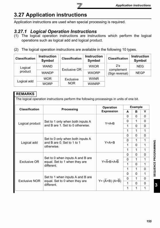
Application instructions
SEQ
UEN
CE
PRO
GR
AM
MIN
G
155
3
3.27 Application instructionsApplication instructions are used when special processing is required.
3.27.1 Logical Operation Instructions(1) The logical operation instructions are instructions which perform the logical
operations such as logical add and logical product.
(2) The logical operation instructions are available in the following 10 types.
Classification Instruction Symbol Classification Instruction
Symbol Classification Instruction Symbol
Logical product
WANDExclusive OR
WXOR 2’s complement
(Sign reversal)
NEG
WANDP WXORP NEGP
Logical addWOR Exclusive
NORWXNR
WORP WXNRP
REMARKSThe logical operation instructions perform the following processings in units of one bit.
Classification Processing Operation Expression
ExampleA B Y
Logical product Set to 1 only when both inputs A and B are 1. Set to 0 otherwise. Y=A•B
0 0 00 1 01 0 01 1 1
Logical addSet to 0 only when both inputs A and B are 0. Set to 1 to 1 otherwise.
Y=A+B
0 0 00 1 11 0 11 1 1
Exclusive ORSet to 0 when inputs A and B are equal. Set to 1 when they are different.
Y=A•B+A•B
0 0 00 1 11 0 11 1 0
Exclusive NORSet to 1 when inputs A and B are equal. Set to 0 when they are different.
Y= (A+B) (A+B)
0 0 10 1 01 0 01 1 1

Application instructions
156
3.27.2 Logical Operation Instructions : 16-bit Logical Product ... WAND, WANDP
Functions
(1) ANDs the 16-bit data of the device specified at and the 16-bit data of thedevice specified at on a bit-by-bit basis, and stores the result into the device
specified at .
Usable Devices
Digit Designation
Error FlagBit devices Word (16-bit)
devices Constants Level
X Y M T C D K H N (M9010, M9011)
WAND K1 to K4
WAND
S
D
S1
S2
D1
WANDP
Operation commands
Operation commands
WAND
WANDP
WAND
Data to be ANDed or head numbers of devices that store data
Head number of device that will store result of logical product.
S
S1
S2
D
D1
DS
D
Before execution
After execution
16 bits

Application instructions
SEQ
UEN
CE
PRO
GR
AM
MIN
G
157
3
(2) ANDs the 16-bit data of the device specified at and the 16-bit data of the
device specified at on a bit-by-bit basis, and stores the result into the device
specified at .
(3) More than the digit designation of a bit device is regarded as 0 for operation.
Execution ConditionsThe execution conditions of the logical product instructions are as shown below.
Program Examples
1)Program that masks the tenth digit (second place from the least significant digit)with 0 among the four BCD digits of D10 when XA turns on.
S1
S2
D1
Before execution
After execution
16 bits
WAND
WANDP
Operation command
Executed every scan.
Executed every scan.
Executed only once.Executed only once.
WAND
Coding(D10)=1234 1204→
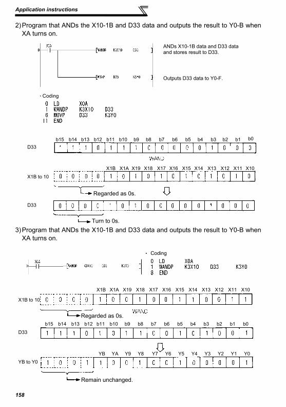
Application instructions
158
2)Program that ANDs the X10-1B and D33 data and outputs the result to Y0-B whenXA turns on.
3)Program that ANDs the X10-1B and D33 data and outputs the result to Y0-B whenXA turns on.
ANDs X10-1B data and D33 data and stores result to D33.
Outputs D33 data to Y0-F.
Coding
X1B to 10
D33
X1B X1A X19 X18 X17 X16 X15 X14 X13 X12 X11 X10
b11 b10 b9 b8 b7 b6 b5 b4 b3 b2 b1 b0b15 b14 b13 b12D33
Regarded as 0s.
Turn to 0s.
Coding
X1B to 10
D33
X1B X1A X19 X18 X17 X16 X15 X14 X13 X12 X11 X10
b11 b10 b9 b8 b7 b6 b5 b4 b3 b2 b1 b0b15 b14 b13 b12
YB YA Y9 Y8 Y7 Y6 Y5 Y4 Y3 Y2 Y1 Y0
YB to Y0
Regarded as 0s.
Remain unchanged.

Application instructions
SEQ
UEN
CE
PRO
GR
AM
MIN
G
159
3
3.27.3 Logical Operation Instructions : 16-bit Logical Add ... WOR, WORP
Functions
(1) ORs the 16-bit data of the device specified at and the 16-bit data of the
device specified at on a bit-by-bit basis, and stores the result into the devicespecified at .
Usable Devices
Digit Designation
Error FlagBit devices Word (16-bit)
devices Constants Level
X Y M T C D K H N (M9010, M9011)
WOR K1 to K4
WOR
S
D
S1
S2
D1
WORP
Operation commands
Operation commands
WOR
WORP
WOR
Data to be ORed or head numbers of devices that store data
Head number of device that will store result of logical add.
S
S1
S2
D
D1
DS
D
Before execution
After execution
16 bits

Application instructions
160
(2) ORs the 16-bit data of the device specified at and the 16-bit data of the device
specified at on a bit-by-bit basis, and stores the result into the device
specified at .
(3) More than the digit designation of a bit device is regarded as 0 for operation.
Execution ConditionsThe execution conditions of the logical add instructions are as shown below.
Program Examples
1)Program that ORs the D10 and D20 data and stores the result into D10 when XAturns on.
S1
S2
D1
Before execution
After execution
16 bits
WOR
WORP
Operation command
Executed every scan.
Executed only once.Executed only once.
Executed everyscan.
WOR
・ Coding
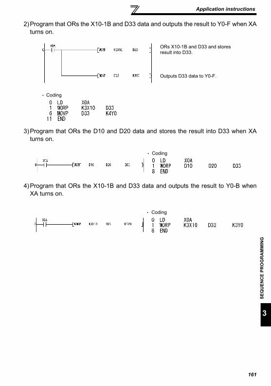
Application instructions
SEQ
UEN
CE
PRO
GR
AM
MIN
G
161
3
2)Program that ORs the X10-1B and D33 data and outputs the result to Y0-F when XAturns on.
3)Program that ORs the D10 and D20 data and stores the result into D33 when XAturns on.
4)Program that ORs the X10-1B and D33 data and outputs the result to Y0-B whenXA turns on.
ORs X10-1B and D33 and stores result into D33.
Outputs D33 data to Y0-F.
Coding
Coding
Coding

Application instructions
162
3.27.4 Logical Operation Instructions : 16-bit Exclusive Logical Add ... WXOR, WXORP
Usable Devices
Digit Designation
Error FlagBit devices Word (16-bit)
devices Constants Level
X Y M T C D K H N (M9010, M9011)
WXOR K1 to K4
S
D
S1
S2
D1
WXORP
Operation commands
Operation commands
WXOR
WXORP
WXOR
Data for which exclusive OR will be performed or head number of device which stores data
Head number of device which will store the result of exclusive OR
S
S1
S2
D
D1

Application instructions
SEQ
UEN
CE
PRO
GR
AM
MIN
G
163
3
Functions
(1) Performs the exclusive OR of the 16-bit data of device specified at and the
16-bit data of device specified at per bit, and stores the result into the devicespecified at .
(2) Performs the exclusive OR of the 16-bit data of device specified at and the
16-bit data of device specified at per bit, and stores the result into the device
specified at .
(3) When operation is performed, the digits of bit device higher than the specified areregarded as 0.
Execution ConditionsThe execution conditions of the exclusive logical add instructions are as shown below.
WXOR
DS
D
16 bits
Before execution
After execution
S1
S2
D
Before execution
After execution
16 bits
WXOR
WXORP
Operation command
Executed every scan.
Executed only once.Executed only once.
Executed everyscan.

Application instructions
164
Program Examples
1)Program which performs exclusive OR of the data of D10 and that of D20, andstores the result to D10 when XA turns on.
2)Program which performs the exclusive OR of the data of X10 to 1B and data of D33,and sends the result to the Y30 to 3B when XA turns on.
3)Program which performs exclusive OR of the data of D10 and that of D20, andstores the result to D33 when XA turns on.
4)Program which performs exclusive OR of the data of X10 to 1B and the data of D33,and sends the result to the Y30 to 3B when XA turns on.
WXOR

Application instructions
SEQ
UEN
CE
PRO
GR
AM
MIN
G
165
3
3.27.5 Logical Operation Instructions : 16-bit NOT Exclusive Logical Add ... WXNR, WXNRP
Usable Devices
Digit Designation
Error FlagBit devices Word (16-bit)
devices Constants Level
X Y M T C D K H N (M9010, M9011)
WXNR K1 to K4
S
D
S1
S2
D1
WXNRP
Operation commands
Operation commands
WXNR
WXNRP
WXNR
Data for which exclusive NOR will be performed or head number of device which stores data
Head number of device which will store the result of exclusive NOR
S
S1
S2
D
D1

Application instructions
166
Functions
(1) Performs the exclusive NOR of the 16-bit data of device specified at and the
16-bit data of device specified at per bit, and stores the result into the devicespecified at .
(2) Performs the exclusive NOR of the 16-bit data of device specified at and the16-bit data of device specified at per bit, and stores the result into the devicespecified at .
(3) When operation is performed, the digits of bit device higher than the specified areregarded as 0.
Execution ConditionsThe execution conditions of the not exclusive logical add instructions are as shownbelow.
WXNR
DS
D
Before execution
After execution
16 bits
S1S2
D
Before execution
After execution
16 bits
WXNR
WXNRP
Operation command
Executed every scan.
Executed only once.Executed only once.
Executed everyscan.

Application instructions
SEQ
UEN
CE
PRO
GR
AM
MIN
G
167
3
Program Examples
1)Program which compares the bit pattern of the 16-bit data of X30 to 3F and that ofthe 16-bit data of D99 and stores the number of the same bit patterns and thenumber of different bit patterns to D7 and 8, respectively, when XC turns on.
2)Program which compares the bit pattern of the 16-bit data of X30 to 3F and that ofthe data of D99 and stores the result to D7 when X0 turns on.
WXNR

Application instructions
168
3.27.6 Logical Operation Instructions : BIN 16-bit 2’s complement ... NEG, NEGP
Functions(1) Reverses the sign of the 16-bit data of device specified at and stores the
result in device specified at .
(2) Used to reverse the positive sign to the negative sign and vice versa.
Usable Devices
Digit Designation
Error FlagBit devices Word (16-bit)
devices Constants Level
X Y M T C D K H N (M9010, M9011)
NEG K1 to K4D
2's complement execution commands
NEG
NEGP
Head number of device which stores data for which 2’ complement will be performed
D
DD
Before execution
Sign
conversion
After execution
16 bits

Application instructions
SEQ
UEN
CE
PRO
GR
AM
MIN
G
169
3
Execution Conditions
Program Examples
1)Program which calculates "D10 - D20" when XA turns on, and obtains the absolutevalue when the result is negative.
NEG
NEG
NEGP
2's complement execution command
Executed every scan.
Executed only once.Executed only once.
Executed everyscan.

170
MEMO

4. ERROR CODE LIST
171
Chapter 1
Chapter 2
Chapter 3
Chapter 4
4.1 How to Read the Error Code .............................. 172

How to Read the Error Code
172
When the built-in PLC function is in the RUN status or if an alarm occurs during RUN,the self-diagnostic function displays the error and stores the error code and error stepinto the special registers. This chapter describes the error definitions and correctiveactions.
4.1 How to Read the Error CodeWhen an error has occurred, the error code can be read with the peripheral device.For the operation method, refer to the operating manual of the peripheral device.The following table indicates the error names, error codes, definitions, causes andcorrective actions.The error code and error step are stored into the following special registers.
Error code.................D9008Error step..................D9010, D9011
Table 4.1 Error Code List
Error NameError Code
(D9008)Status Definition and Cause Corrective Action
“INSTRCT CODE ERR.”[Checked at instructionexecution]
10 Stop
The instruction code that cannot be decoded is included in the program.• The memory contents
changed for some reason.
Read the error step using GX Developer, and correct that step in the program.
“PARAMETER ERROR”[Checked at power-on or STOP to RUN] 11 Stop
(1) Write to the CPU was performed after the capacity larger than the memory capacity of the CPU was set using GX Developer.
(2) The parameter data of the CPU memory changed due to noise or memory loading fault.
Check the memory capacity of the CPU with the memory capacity set using GX Developer, and re-set using GX Developer.
“WDT ERROR”[Checked at END processing execution]
22 Stop
The scan time exceeds the watchdog error monitor time.• The user program scan
time has increased.
Calculate/check the user program scan time and reduce the scan time.
“END NOT EXECUTE”[Checked at END instruction execution]l 24 Stop
(1) The END instruction has been read as another instruction code due to noise, etc.
(2) The END instruction has changed into another instruction code for some reason.
Reset and RUN again. If the same error appears again, the cause is a CPU hardware fault. Consult the Mitsubishi representative.

How to Read the Error Code
ERR
OR
CO
DE
LIST
173
4
“OPERATION ERROR”[Checked at instruction execution]
50 Run(Stop)
Divided by zero Read the error step by use of peripheral device, and check and correct the program at that step.
Error NameError Code
(D9008)Status Definition and Cause Corrective Action

174
MEMO

APPENDIX
175
Appendix1Instruction Processing Time .................... 176

Instruction Processing Time
176
Appendix1 Instruction Processing Time
Instruction Condition (Device)
Number of Steps
Processing Time (µs)
LD 1 2.6 LDI 1 2.7 AND 1 2.8 ANI 1 2.8 OR 1 2.7 ORI 1 2.8 ORB 1 2.0 ANB 1 2.0 MPS 1 1.9 MRD 1 1.9 MPP 1 2.0 MC 5 3.7 MCR 3 2.4 NOP 1 2.1 NOPLF 1 2.1 END 1 1.3 PLS 3 3.6 PLF 3 3.5 SFT 3 3.6 SFTP 3 4.1
OUT
Y,M 1 2.5 Special M 3 3.2 T 1 2.5 C 1 2.6
SETY,M 1 2.5 Special M 3 3.1
RST
Y,M 1 2.6 Special M 3 3.3 T 3 3.8 C 3 3.8 D 3 3.2
MOV 5 7.7 MOVP 5 8.5 WAND 5 10.3 WANDP 5 10.7 WAND 7 10.1 WANDP 7 10.7 WOR 5 10.3 WORP 5 10.7
WOR 7 10.2 WORP 7 10.6 WXOR 5 10.4 WXORP 5 10.8 WXOR 7 10.3 WXORP 7 10.7 WXNR 5 10.5 WXNRP 5 10.9 WXNR 7 10.3 WXNRP 7 10.7 NEG 3 7.7 NEGP 3 8.1 LD= 5 7.7 LD= 7 8.3 LD<> 5 7.8 LD<> 7 8.3 LD> 5 7.7 LD> 7 8.3 LD<= 5 7.8 LD<= 7 8.3 LD< 5 7.8 LD< 7 8.3 LD>= 5 7.9 LD>= 7 8.3 AND= 5 7.3 AND= 7 7.5 AND<> 5 7.4 AND<> 7 7.5 AND> 5 7.4 AND> 7 7.5 AND<= 5 7.5 AND<= 7 7.7 AND< 5 7.4 AND< 7 7.7 AND>= 5 7.5 AND>= 7 7.7 OR= 5 7.4 OR= 7 8.1 OR<> 5 7.5
Instruction Condition (Device)
Number of Steps
Processing Time (µs)

Instruction Processing Time
177
OR<> 7 8.2 OR> 5 7.5 OR> 7 8.2 OR<= 5 7.5 OR<= 7 8.2 OR< 5 7.5 OR< 7 8.2 OR>= 5 7.6 OR>= 7 8.2 + 5 10.3 +P 5 10.7 + 7 10.3 +P 7 10.7 - 5 10.3 -P 5 10.7 - 7 10.4 -P 7 10.8 * 7 10.8 *P 7 11.3 / 7 11.3 /P 7 11.8
Instruction Condition (Device)
Number of Steps
Processing Time (µs)
REMARKSAs inverter control is also performed actually, the scan time is approximately 40ms at 500steps.

REVISIONS*The manual number is given on the bottom left of the back cover
Print Date *Manual Number RevisionSep., 2005 IB(NA)-0600262ENG-A First edition