FPGA vs CPLD
27
ArchitectureofFPGAsandCPLDs:ATutorial StephenBrownandJonathanRose DepartmentofElectricalandComputerEngineering UniversityofToronto email:brown|[email protected] Abstract Thispaperprovidesa tutorialsurveyofarchitecturesofcommercially available high-capacity field-programmabledevices(FPDs).Wefirstdefinetherelevantterminologyint hefieldandthen describetherecentevolutionofFPDs.ThethreemaincategoriesofFPDsaredel ineated:Simple PLDs(SPLDs),Complex PLDs(CPLDs)andField-ProgrammableGateArrays(FPGAs).W e thengivedetailsoft hearchitecturesofall ofthemostimportantcom mercially availablechips, andgiveexamplesofapplicationsofeachtypeofdevice. Page2of41 1IntroductiontoHigh-CapacityFPDs Promptedbythedevelo pmentofnewtypesofso phisticatedfield-program mabledev ices(FPDs), theprocessofdesigningdigitalhardwarehas changeddramaticallyover thepast fewyears. Unlikepreviousgenera tionsoftechnology,in whichboard-leveldesigns included largenumbers ofSSIchipscontainingbasicgates,virtually everydigitaldesignpro ducedtod ayconsistsmostly ofhigh-densitydevices.Thisappliesnotonly tocustomdeviceslikep rocessors andmemory,but alsoforlogiccircuitssuchasstatemachine controllers,counters,registers, anddecoders.When suchcircuitsaredestinedforhigh-volumesystemstheyhavebeenintegratedint ohigh-density gatearrays.However, gatearrayNREcostsoftenaretooexpensiveand gatearra ystaketoolong tomanufacturetobeviableforprototypingor otherlow-volumescenari os.Fort hesereasons, mostprototypes,anda lsomanyproductiondesignsarenowbuiltusingFPDs.The mostcompelling advantagesofFPDsare instantmanufacturingt urnaround,lowstart-upcosts,low financial riskand(sinceprogrammingisdonebytheend user)easeofdesigncha nges. ThemarketforFPDsha sgrowndramaticallyove rthepastdecadetothe pointwhe rethereis nowawideassortment ofdevicestochoosefrom.Adesignertodayfaces adaunti ngtaskto researchthedifferent typesofchips,understandwhattheycanbestbe usedfor ,chooseaparticular manufacturers’sproduc t,learntheintricacies ofvendor-specificsoftw areandthe ndesignthe hardware.Confusionfordesignersisexacerbatedbynotonlythesheer numberof FPDsavailable, butalsobythecomple xityofthemoresophisticateddevices.Thepurposeofthi spaperisto provideanoverviewof thearchitectureofthe varioustypesofFPDs.T heemphas isisondevices withrelativelyhighl ogiccapacity;allofthemostimportantcommercialproduc tsarediscussed. Beforeproceeding,we providedefinitionsoftheterminologyinthisfield.This isnecessary
Transcript of FPGA vs CPLD

7/31/2019 FPGA vs CPLD
http://slidepdf.com/reader/full/fpga-vs-cpld 1/27
ArchitectureofFPGAsandCPLDs:ATutorialStephenBrownandJonathanRoseDepartmentofElectricalandComputerEngineeringUniversityofTorontoemail:brown|jayar@eecg.toronto.eduAbstractThispaperprovidesatutorialsurveyofarchitecturesofcommerciallyavailablehigh-capacityfield-programmabledevices(FPDs).WefirstdefinetherelevantterminologyinthefieldandthendescribetherecentevolutionofFPDs.ThethreemaincategoriesofFPDsaredelineated:SimplePLDs(SPLDs),ComplexPLDs(CPLDs)andField-ProgrammableGateArrays(FPGAs).Wethengivedetailsofthearchitecturesofallofthemostimportantcommerciallyavailablechips,andgiveexamplesofapplicationsofeachtypeofdevice.Page2of411IntroductiontoHigh-CapacityFPDsPromptedbythedevelopmentofnewtypesofsophisticatedfield-programmabledevices(FPDs),theprocessofdesigningdigitalhardwarehaschangeddramaticallyoverthepastfewyears.Unlikepreviousgenerationsoftechnology,inwhichboard-leveldesignsincluded
largenumbersofSSIchipscontainingbasicgates,virtuallyeverydigitaldesignproducedtodayconsistsmostlyofhigh-densitydevices.Thisappliesnotonlytocustomdeviceslikeprocessorsandmemory,butalsoforlogiccircuitssuchasstatemachinecontrollers,counters,registers,anddecoders.Whensuchcircuitsaredestinedforhigh-volumesystemstheyhavebeenintegratedintohigh-densitygatearrays.However,gatearrayNREcostsoftenaretooexpensiveandgatearraystaketoolongtomanufacturetobeviableforprototypingorotherlow-volumescenarios.Forthesereasons,
mostprototypes,andalsomanyproductiondesignsarenowbuiltusingFPDs.ThemostcompellingadvantagesofFPDsareinstantmanufacturingturnaround,lowstart-upcosts,lowfinancialriskand(sinceprogrammingisdonebytheenduser)easeofdesignchanges.ThemarketforFPDshasgrowndramaticallyoverthepastdecadetothepointwherethereisnowawideassortmentofdevicestochoosefrom.Adesignertodayfacesadauntingtasktoresearchthedifferenttypesofchips,understandwhattheycanbestbeusedfor,chooseaparticularmanufacturers’sproduct,learntheintricaciesofvendor-specificsoftwareandthendesignthe
hardware.ConfusionfordesignersisexacerbatedbynotonlythesheernumberofFPDsavailable,butalsobythecomplexityofthemoresophisticateddevices.ThepurposeofthispaperistoprovideanoverviewofthearchitectureofthevarioustypesofFPDs.Theemphasisisondeviceswithrelativelyhighlogiccapacity;allofthemostimportantcommercialproductsarediscussed.Beforeproceeding,weprovidedefinitionsoftheterminologyinthisfield.Thisisnecessary

7/31/2019 FPGA vs CPLD
http://slidepdf.com/reader/full/fpga-vs-cpld 2/27
becausethetechnicaljargonhasbecomesomewhatinconsistentoverthepastfewyearsascompanieshaveattemptedtocompareandcontrasttheirproductsinliterature.Page3of411.1DefinitionsofRelevantTerminologyThemostimportantterminologyusedinthispaperisdefinedbelow.•Field-ProgrammableDevice(FPD)—ageneraltermthatreferstoanytypeofintegratedcircuitusedforimplementingdigitalhardware,wherethechipcanbeconfiguredbytheendusertorealizedifferentdesigns.Programmingofsuchadeviceofteninvolvesplacingthechipintoaspecialprogrammingunit,butsomechipscanalsobeconfigured“in-system”.AnothernameforFPDsisprogrammablelogicdevices(PLDs);althoughPLDsencompassthesametypesofchipsasFPDs,wepreferthetermFPDbecausehistoricallythewordPLDhasreferredtorelativelysimpletypesofdevices.•PLA—aProgrammableLogicArray(PLA)isarelativelysmallFPDthatcontainstwolevelsoflogic,anAND-planeandanOR-plane,wherebothlevelsareprogrammable(note:althoughPLAstructuresaresometimesembeddedintofull-customchips,wereferhereonly
tothosePLAsthatareprovidedasseparateintegratedcircuitsandareuser-programmable).•PAL*—aProgrammableArrayLogic(PAL)isarelativelysmallFPDthathasaprogrammableAND-planefollowedbyafixedOR-plane•SPLD—referstoanytypeofSimplePLD,usuallyeitheraPLAorPAL•CPLD—amoreComplexPLDthatconsistsofanarrangementofmultipleSPLD-likeblocksonasinglechip.Alternativenames(thatwillnotbeusedinthispaper)sometimesadoptedforthisstyleofchipareEnhancedPLD(EPLD),SuperPAL,MegaPAL,andothers.•FPGA—aField-ProgrammableGateArrayisanFPDfeaturingageneralstructuretha
tallowsveryhighlogiccapacity.WhereasCPLDsfeaturelogicresourceswithawidenumberofinputs(ANDplanes),FPGAsoffermorenarrowlogicresources.FPGAsalsoofferahigherratioofflip-flopstologicresourcesthandoCPLDs.•HCPLDs—high-capacityPLDs:asingleacronymthatreferstobothCPLDsandFPGAs.Thistermhasbeencoinedintradeliteratureforprovidinganeasywaytorefertobothtypesofdevices.Wedonotusethisterminthepaper.*PALisatrademarkofAdvancedMicroDevices.Page4of41
•Interconnect—thewiringresourcesinanFPD.•ProgrammableSwitch—auser-programmableswitchthatcanconnectalogicelementtoaninterconnectwire,oroneinterconnectwiretoanother•LogicBlock—arelativelysmallcircuitblockthatisreplicatedinanarrayinanFPD.WhenacircuitisimplementedinanFPD,itisfirstdecomposedintosmallersub-circuitsthatcaneachbemappedintoalogicblock.ThetermlogicblockismostlyusedinthecontextofFPGAs,but

7/31/2019 FPGA vs CPLD
http://slidepdf.com/reader/full/fpga-vs-cpld 3/27
itcouldalsorefertoablockofcircuitryinaCPLD.•LogicCapacity—theamountofdigitallogicthatcanbemappedintoasingleFPD.Thisisusuallymeasuredinunitsof“equivalentnumberofgatesinatraditionalgatearray”.Inotherwords,thecapacityofanFPDismeasuredbythesizeofgatearraythatitiscomparableto.Insimplerterms,logiccapacitycanbethoughtofas“numberof2-inputNANDgates”.•LogicDensity—theamountoflogicperunitareainanFPD.•Speed-Performance—measuresthemaximumoperablespeedofacircuitwhenimplementedinanFPD.Forcombinationalcircuits,itissetbythelongestdelaythroughanypath,andforsequentialcircuitsitisthemaximumclockfrequencyforwhichthecircuitfunctionsproperly.Intheremainderofthissection,toprovideinsightintoFPDdevelopmenttheevolutionofFPDsoverthepasttwodecadesisdescribed.AdditionalbackgroundinformationisalsoincludedonthesemiconductortechnologiesusedinthemanufactureofFPDs.1.2EvolutionofProgrammableLogicDevicesThefirsttypeofuser-programmablechipthatcouldimplementlogiccircuitswastheProgrammableRead-OnlyMemory(PROM),inwhichaddresslinescanbeusedaslogiccircuitinp
utsanddatalinesasoutputs.Logicfunctions,however,rarelyrequiremorethanafewproductterms,andaPROMcontainsafulldecoderforitsaddressinputs.PROMSarethusaninefficientarchitectureforrealizinglogiccircuits,andsoarerarelyusedinpracticeforthatpurpose.ThefirstdevicedevelopedlaterspecificallyforimplementinglogiccircuitswastheField-ProgrammableLogicArray(FPLA),orsimplyPLAforshort.APLAconsistsoftwolevelsoflogicgates:aprogramPage5of41mable“wired”AND-planefollowedbyaprogrammable“wired”OR-plane.APLAisstructure
sothatanyofitsinputs(ortheircomplements)canbeAND’edtogetherintheAND-plane;eachAND-planeoutputcanthuscorrespondtoanyproducttermoftheinputs.Similarly,eachORplaneoutputcanbeconfiguredtoproducethelogicalsumofanyoftheAND-planeoutputs.Withthisstructure,PLAsarewell-suitedforimplementinglogicfunctionsinsum-of-productsform.Theyarealsoquiteversatile,sinceboththeANDtermsandORtermscanhavemanyinputs(thisfeatureisoftenreferredtoaswideANDandORgates).WhenPLAswereintroducedintheearly1970s,byPhilips,theirmaindrawbackswerethat
theywereexpensivetomanufactureandofferedsomewhatpoorspeed-performance.Bothdisadvantageswereduetothetwolevelsofconfigurablelogic,becauseprogrammablelogicplanesweredifficulttomanufactureandintroducedsignificantpropagationdelays.Toovercometheseweaknesses,ProgrammableArrayLogic(PAL)devicesweredeveloped.AsFigure1illustrates,PALsfeatureonlyasinglelevelofprogrammability,consistingofaprogrammable“wired”ANDplane

7/31/2019 FPGA vs CPLD
http://slidepdf.com/reader/full/fpga-vs-cpld 4/27
thatfeedsfixedOR-gates.TocompensateforlackofgeneralityincurredbecausetheOROutputsPlaneANDInputs&Flip−flopfeedbacksDDDDDDFigure1-StructureofaPAL.Page6of41planeisfixed,severalvariantsofPALsareproduced,withdifferentnumbersofinputsandoutputs,andvarioussizesofOR-gates.PALsusuallycontainflip-flopsconnectedtotheOR-gateoutputssothatsequentialcircuitscanberealized.PALdevicesareimportantbecausewhenintroducedtheyhadaprofoundeffectondigitalhardwaredesign,andalsotheyarethebasisforsomeofthenewer,moresophisticatedarchitecturesthatwillbedescribedshortly.VariantsofthebasicPALarchitecturearefeaturedinseveralotherproductsknownbydifferent
acronyms.AllsmallPLDs,includingPLAs,PALs,andPAL-likedevicesaregroupedintoasinglecategorycalledSimplePLDs(SPLDs),whosemostimportantcharacteristicsarelowcostandveryhighpin-to-pinspeed-performance.Astechnologyhasadvanced,ithasbecomepossibletoproducedeviceswithhighercapacitythanSPLDs.ThedifficultywithincreasingcapacityofastrictSPLDarchitectureisthatthestructureoftheprogrammablelogic-planesgrowtooquicklyinsizeasthenumberofinputsisincreased.TheonlyfeasiblewaytoprovidelargecapacitydevicesbasedonSPLD
architecturesisthentointegratemultipleSPLDsontoasinglechipandprovideinterconnecttoprogrammablyconnecttheSPLDblockstogether.ManycommercialFPDproductsexistonthemarkettodaywiththisbasicstructure,andarecollectivelyreferredtoasComplexPLDs(CPLDs).CPLDswerepioneeredbyAltera,firstintheirfamilyofchipscalledClassicEPLDs,andtheninthreeadditionalseries,calledMAX5000,MAX7000andMAX9000.BecauseofarapidlygrowingmarketforlargeFPDs,othermanufacturersdevelopeddevicesintheCPLDcategoryand
therearenowmanychoicesavailable.AllofthemostimportantcommercialproductswillbedescribedinSection2.CPLDsprovidelogiccapacityuptotheequivalentofabout50typicalSPLDdevices,butitissomewhatdifficulttoextendthesearchitecturestohigherdensities.TobuildFPDswithveryhighlogiccapacity,adifferentapproachisneeded.Page7of41Thehighestcapacitygeneralpurposelogicchipsavailabletodayarethetraditionalgatearrays

7/31/2019 FPGA vs CPLD
http://slidepdf.com/reader/full/fpga-vs-cpld 5/27
sometimesreferredtoasMask-ProgrammableGateArrays(MPGAs).MPGAsconsistofanarrayofpre-fabricatedtransistorsthatcanbecustomizedintotheuser’slogiccircuitbyconnectingthetransistorswithcustomwires.Customizationisperformedduringchipfabricationbyspecifyingthemetalinterconnect,andthismeansthatinorderforausertoemployanMPGAalargesetupcostisinvolvedandmanufacturingtimeislong.AlthoughMPGAsareclearlynotFPDs,theyarementionedherebecausetheymotivatedthedesignoftheuser-programmableequivalent:Field-ProgrammableGateArrays(FPGAs).LikeMPGAs,FPGAscompriseanarrayofuncommittedcircuitelements,calledlogicblocks,andinterconnectresources,butFPGAconfigurationisperformedthroughprogrammingbytheenduser.AnillustrationofatypicalFPGAarchitectureappearsinFigure2.AstheonlytypeofFPDthatsupportsveryhighlogiccapacity,FPGAshavebeenresponsibleforamajorshiftinthewaydigitalcircuitsaredesigned.Figure2-StructureofanFPGA.BlockLogic
I/OBlockPage8of41Figure3summarizesthecategoriesofFPDsbylistingthelogiccapacitiesavailableineachofthethreecategories.Inthefigure,“equivalentgates”referslooselyto“numberof2-inputNANDgates”.Thechartservesasaguideforselectingaspecificdeviceforagivenapplication,dependingonthelogiccapacityneeded.However,aswewilldiscussshortly,eachtypeofFPDisinherentlybettersuitedforsomeapplicationsthanforothers.Itshouldalsobementionedthatthereexistotherspecial-purposedevicesoptimizedforspecificapplications(e.g.st
atemachines,analoggatearrays,largeinterconnectionproblems).However,sinceuseofsuchdevicesislimitedtheywillnotbedescribedhere.Thenextsub-sectiondiscussesthemethodsusedtoimplementtheuser-programmableswitchesthatarethekeytotheuser-customizationofFPDs.1.3User-ProgrammableSwitchTechnologiesThefirsttypeofuser-programmableswitchdevelopedwasthefuseusedinPLAs.Althoughfusesarestillusedinsomesmallerdevices,wewillnotdiscussthemherebecausetheyarequicklybeingreplacedbynewertechnology.Forhigherdensitydevices,whereCMOSdominatestheIC
industry,differentapproachestoimplementingprogrammableswitcheshavebeendeveloped.ForCPLDsthemainswitchtechnologies(incommercialproducts)arefloatinggatetransistorslikeFigure3-FPDCategoriesbyLogicCapacity.1000200200020000Equivalent

7/31/2019 FPGA vs CPLD
http://slidepdf.com/reader/full/fpga-vs-cpld 6/27
GatesSPLDsCPLDsFPGAs12000500040000******Legend******AlteraMAX9000AlteraFLEX10000,AT&TORCA2AlteraMAX7000,AMDMach,Lattice(p)LSI,CypressFLASH370,XilinxXC9500Page9of41thoseusedinEPROMandEEPROM,andforFPGAstheyareSRAMandantifuse.Eachoftheseisbrieflydiscussedbelow.AnEEPROMorEPROMtransistorisusedasaprogrammableswitchforCPLDs(andalsoformanySPLDs)byplacingthetransistorbetweentwowiresinawaythatfacilitatesimplementationofwired-ANDfunctions.ThisisillustratedinFigure4,whichshowsEPROMtrans
istorsastheymightbeconnectedinanAND-planeofaCPLD.AninputtotheAND-planecandriveaproductwiretologiclevel‘0’throughanEPROMtransistor,ifthatinputispartofthecorrespondingproductterm.Forinputsthatarenotinvolvedforaproductterm,theappropriateEPROMtransistorsareprogrammedtobepermanentlyturnedoff.AdiagramforanEEPROMbaseddevicewouldlooksimilar.AlthoughthereisnotechnicalreasonwhyEPROMorEEPROMcouldnotbeappliedtoFPGAs,currentcommercialFPGAproductsarebasedeitheronSRAMorantifusetec
hnologies,asdiscussedbelow.AnexampleofusageofSRAM-controlledswitchesisillustratedinFigure5,showingtwoapplicationsofSRAMcells:forcontrollingthegatenodesofpass-transistorswitchesandtocon-+5VEPROMinputwireEPROMinputwireproductwireFigure4-EPROMProgrammableSwitches.
Page10of41troltheselectlinesofmultiplexersthatdrivelogicblockinputs.Thefiguresgivesanexampleoftheconnectionofonelogicblock(representedbytheAND-gateintheupperleftcorner)toanotherthroughtwopass-transistorswitches,andthenamultiplexer,allcontrolledbySRAMcells.WhetheranFPGAusespass-transistorsormultiplexersorbothdependsontheparticularproduct.

7/31/2019 FPGA vs CPLD
http://slidepdf.com/reader/full/fpga-vs-cpld 7/27
TheothertypeofprogrammableswitchusedinFPGAsistheantifuse.Antifusesareoriginallyopen-circuitsandtakeonlowresistanceonlywhenprogrammed.AntifusesaresuitableforFPGAsbecausetheycanbebuiltusingmodifiedCMOStechnology.Asanexample,Actel’santifusestructure,knownasPLICE[Ham88],isdepictedinFigure6.Thefigureshowsthatanantifuseispositionedbetweentwointerconnectwiresandphysicallyconsistsofthreesandwichedlayers:thetopandbottomlayersareconductors,andthemiddlelayerisaninsulator.Whenunprogrammed,theinsulatorisolatesthetopandbottomlayers,butwhenprogrammedtheinsulatorchangestobecomealow-resistancelink.PLICEusesPoly-Siandn+diffusionasconductorsSRAMLogicCellLogicCellLogicCellLogicCellSRAMSRAMFigure5-SRAM-controlledProgrammableSwitches.Page11of41andONO(see[Ham88])asaninsulator,butotherantifusesrelyonmetalforcon
ductors,withamorphoussiliconasthemiddlelayer[Birk92][Marp94].Table1liststhemostimportantcharacteristicsoftheprogrammingtechnologiesdiscussedinthissection.Theleft-mostcolumnofthetableindicateswhethertheprogrammableswitchesareone-timeprogrammable(OTP),orcanbere-programmed(RP).Thenextcolumnlistswhethertheswitchesarevolatile,andthelastcolumnnamestheunderlyingtransistortechnology.NameRe-programmableVolatileTechnologyFusenonoBipolarEPROMyes
outofcircuitnoUVCMOSEEPROMyesincircuitnoEECMOSSRAMyesincircuityesCMOSAntifusenonoCMOS+Table1-SummaryofProgrammingTechnologies.siliconsubstraten+diffisiondielectric
oxidePoly−SiwirewireantifuseFigure6-ActelAntifuseStructure.Page12of411.4ComputerAidedDesign(CAD)FlowforFPDsWhendesigningcircuitsforimplementationinFPDs,itisessentialtoemployComputer-AidedDesign(CAD)programs.Suchsoftwaretoolsarediscussedbrieflyinthissection

7/31/2019 FPGA vs CPLD
http://slidepdf.com/reader/full/fpga-vs-cpld 8/27
toprovideafeelforthedesignprocessinvolved.CADtoolsareimportantnotonlyforcomplexdeviceslikeCPLDsandFPGAs,butalsoforSPLDs.AtypicalCADsystemforSPLDswouldincludesoftwareforthefollowingtasks:initialdesignentry,logicoptimization,devicefitting,simulation,andconfiguration.ThisdesignflowisillustratedinFigure7,whichalsoindicateshowsomestagesfeedbacktoothers.DesignentrymaybedoneeitherbycreatingaschematicdiagramwithagraphicalCADtool,byusingatextbasedsystemtodescribeadesigninasimplehardwaredescriptionlanguage,orwithamixtureofdesignentrymethods.Sinceinitiallogicentryisnotusuallyinanoptimizedform,algorithmsareemployedtooptimizethecircuits,afterwhichadditionalalgorithmsanalysetheresultinglogicequationsand“fit”themintotheSPLD.Simulationisusedtoverifycorrectoperation,andtheuserwouldreturntothedesignentrysteptofixerrors.WhenadesignsimulatescorrectlyitcanbeloadedintoaprogrammingunitandusedtoconfigureanSPLD.OnefinaldetailtonoteaboutFigure
7isthatwhiletheoriginaldesignentrystepisperformedmanuallybythedesigner,allotherstepsarecarriedoutautomaticallybymostCADsystems.schematiccapturetextentrysimulateSPLDfixerrorsconfigurationfilemanualautomaticmerge&
translateoptimizeequationsdevicefitterFigure7-CADDesignFlowforSPLDs.ProgrammingUnitPage13of41ThestepsinvolvedforimplementingcircuitsinCPLDsaresimilartothoseforSPLDs,butthetoolsthemselvesaremoresophisticated.Becausethedevicesarecomplexandcanaccommodatelargedesigns,itismorecommontouseamixtureofdesignentrymethodsfordi
fferentmodulesofacompletecircuit.Forinstance,somemodulesmightbedesignedwithasmallhardwaredescriptionlanguagelikeABEL,othersdrawnusingasymbolicschematiccapturetool,andstillothersdescribedviaafull-featuredhardwaredescriptionlanguagesuchasVHDL.Also,forCPLDstheprocessof“fitting”adesignmayrequirestepssimilartothosedescribedbelowforFPGAs,dependingonhowsophisticatedtheCPLDis.Thenecessarysoftwareforth

7/31/2019 FPGA vs CPLD
http://slidepdf.com/reader/full/fpga-vs-cpld 9/27
esetasksissuppliedeitherbytheCPLDmanufacturerorathirdparty.ThedesignprocessforFPGAsissimilartothatforCPLDs,butadditionaltoolsareneededtosupporttheincreasedcomplexityofthechips.Themajordifferenceisinthe“devicefitter”stepthatcomesafterlogicoptimizationandbeforesimulation,whereFPGAsrequireatleastthreesteps:atechnologymappertomapfrombasiclogicgatesintotheFPGA’slogicblocks,placementtochoosewhichspecificlogicblockstouseintheFPGA,andaroutertoallocatethewiresegmentsintheFPGAtointerconnectthelogicblocks.Withthisaddedcomplexity,theCADtoolsmightrequireafairlylongperiodoftime(oftenmorethananhourorevenseveralhours)tocompletetheirtasks.2OverviewofCommerciallyAvailableFPDsThissectionprovidesmanyexamplesofcommercialFPDproducts.SPLDsarefirstdiscussedbriefly,andthendetailsaregivenforallofthemostimportantCPLDsandFPGAs.Thereaderwhoisinterestedinmoredetailsonthecommercialproductsisencouragedtocontactthemanufacturers,
ortheirdistributors,forthelatestdatasheets*.*MostFPDmanufacturersnowprovidetheirdatasheetsontheworldwideweb,andcanbelocatedatURL“http://www.companyname.com”.Page14of412.1CommerciallyAvailableSPLDsAsthestaplefordigitalhardwaredesignersforthepasttwodecades,SPLDsareveryimportantdevices.SPLDsrepresentthehighestspeed-performanceFPDsavailable,andareinexpensive.However,theyarealsofairlystraight-forwardandwellunderstood,sothispaperwilldiscussthemonlybriefly.
TwoofthemostpopularSPLDsarethePALsproducedbyAdvancedMicroDevices(AMD)knownasthe16R8and22V10.Bothofthesedevicesareindustrystandardsandarewidelysecond-sourcedbyvariouscompanies.Thename“16R8”meansthatthePALhasamaximumof16inputs(thereare8dedicatedinputsand8input/outputs),andamaximumof8outputs.The“R”referstothetypeofoutputsprovidedbythePALandmeansthateachoutputis“registered”byaDflip-flop.Similarly,the“22V10”hasamaximumof22inputsand10outputs.Here,the“V”meanseachoutputis“versatile”andcanbeconfiguredinvariousways,someconfigurationsregistered
andsomenot.AnotherwidelyusedandsecondsourcedSPLDistheAlteraClassicEP610.ThisdeviceissimilarincomplexitytoPALs,butitoffersmoreflexibilityinthewaythatoutputsareproducedandhaslargerAND-andOR-planes.IntheEP610,outputscanberegisteredandtheflip-flopsareconfigurableasanyofD,T,JK,orSR.InadditiontotheSPLDsmentionedabovemanyotherproductsareavailablefromawide

7/31/2019 FPGA vs CPLD
http://slidepdf.com/reader/full/fpga-vs-cpld 10/27
arrayofcompanies.AllSPLDssharecommoncharacteristics,likesomesortoflogicplanes(AND,OR,NOR,orNAND),buteachspecificproductoffersuniquefeaturesthatmaybeparticularlyattractiveforsomeapplications.ApartiallistofcompaniesthatofferSPLDsincludes:AMD,Altera,ICT,Lattice,Cypress,andPhilips-Signetics.SincesomeoftheseSPLDshavecomplexityapproachingthatfoundinCPLDs,thepaperwillnowmoveontomoresophisticateddevices.Page15of412.2CommerciallyAvailableCPLDsAsstatedearlier,CPLDsconsistofmultipleSPLD-likeblocksonasinglechip.However,CPLDproductsaremuchmoresophisticatedthanSPLDs,evenattheleveloftheirbasicSPLD-likeblocks.Inthissection,CPLDsarediscussedindetail,firstbysurveyingtheavailablecommercialproductsandthenbydiscussingthetypesofapplicationsforwhichCPLDsarebestsuited.Sufficientdetailsarepresentedtoallowacomparisonbetweenthevariouscompetingproducts,withmoreattentionbeingpaidtodevicesthatwebelieveareinmorewidespreaduse
thanothers.2.2.1AlteraCPLDsAlterahasdevelopedthreefamiliesofchipsthatfitwithintheCPLDcategory:MAX5000,MAX7000,andMAX9000.Here,thediscussionwillfocusontheMAX7000series,becauseitiswidelyusedandoffersstate-of-the-artlogiccapacityandspeed-performance.MAX5000representsanoldertechnologythatoffersacosteffectivesolution,andMAX9000issimilartoMAX7000,exceptthatMAX9000offershigherlogiccapacity(theindustry’shighestforCPLDs).ThegeneralarchitectureoftheAlteraMAX7000seriesisdepictedinFigure8.
ItcomprisesanarrayofblockscalledLogicArrayBlocks(LABs),andinterconnectwirescalledaProgram-Figure8-AlteraMAX7000Series.PIALABI/OBlockPage16of41mableInterconnectArray(PIA).ThePIAiscapableofconnectinganyLABinputoroutputtoanyotherLAB.Also,theinputsandoutputsofthechipconnectdirectlytothePIAandtoLABs.
ALABcanbethoughtofasacomplexSPLD-likestructure,andsotheentirechipcanbeconsideredtobeanarrayofSPLDs.MAX7000devicesareavailablebothbasedinEPROMandEEPROMtechnology.Untilrecently,evenwithEEPROM,MAX7000chipscouldbeprogrammableonly“out-of-circuit”inaspecial-purposeprogrammingunit;however,in1996Alterareleasedthe7000Sseries,whichisreprogrammable“in-circuit”.ThestructureofaLABisshowninFigure9.EachLABconsistsoftwosetsofeightmacrocells(showninFigure10),whereamacrocellcomprisesasetofprogrammableproduct

7/31/2019 FPGA vs CPLD
http://slidepdf.com/reader/full/fpga-vs-cpld 11/27
terms(partofanAND-plane)thatfeedsanOR-gateandaflip-flop.Theflip-flopscanbeconfiguredasDtype,JK,T,SR,orcanbetransparent.AsillustratedinFigure10,thenumberofinputstotheFigure9-AlteraMAX7000LogicArrayBlock(LAB).LABMacrocellsArrayof16AIPtoI/OCellsI/OControlBlockfromI/OpinstootherLABsproduct-termsharingPage17of41OR-gateinamacrocellisvariable;theOR-gatecanbefedfromanyorallofthefiveproducttermswithinthemacrocell,andinadditioncanhaveupto15extraproducttermsfrommacrocellsinthesameLAB.ThisproducttermflexibilitymakestheMAX7000seriesLABmoreefficientin
termsofchipareabecausetypicallogicfunctionsdonotneedmorethanfiveproductterms,andthearchitecturesupportswiderfunctionswhentheyareneeded.ItisinterestingtonotethatvariablesizedOR-gatesofthissortarenotavailableinbasicSPLDs(seeFigure1).SimilarfeaturesofthiskindarefoundinotherCPLDarchitecturesdiscussedshortly.BesidesAltera,severalothercompaniesproducedevicesthatcanbecategorizedasCPLDs.Forexample,AMDmanufacturerstheMachfamily,Latticehasthe(i)pLSIseries,XilinxproducesaCPLDseriesthattheycallXC7000(unrelatedtotheAlteraMAX7000series)andhas
announcedanewfamilycalledXC9500,andICThasthePEELarray.Thesedevicesarediscussedinthefollowingsub-sections.Figure10-MAX7000Macrocell.MatrixProductSelectPIALocalLABInterconnectnotshown)(globalclearclearGlobalclock
arrayclockRDQStoPIAsetinputsfromothermacrocellsinLABstatePage18of41

7/31/2019 FPGA vs CPLD
http://slidepdf.com/reader/full/fpga-vs-cpld 12/27
2.2.2AdvancedMicroDevices(AMD)CPLDsAMDoffersaCPLDfamilywithfivesub-familiescalledMach1toMach5.EachMachdevicecomprisesmultiplePAL-likeblocks:Mach1and2consistofoptimized22V16PALs,andMach3and4compriseseveraloptimized34V16PALs,andMach5issimilarbutoffersenhancedspeedperformance.AllMachchipsarebasedonEEPROMtechnology,andtogetherthefivesub-familiesprovideawiderangeofselection,fromsmall,inexpensivechipstolargerstate-of-the-artones.ThisdiscussionwillfocusonMach4,becauseitrepresentsthemostadvancedcurrentlyavailablepartsintheMachfamily.Figure11depictsaMach4chip,showingthemultiple34V16PAL-likeblocks,andtheinterconnect,calledCentralSwitchMatrix,forconnectingtheblockstogether.Chipsrangeinsizefrom6to16PALblocks,whichcorrespondsroughlyto2000to5000equivalentgatesandareincircuitprogrammable.AllconnectionsinMach4betweenonePALblockandanother(evenfromaPALblocktoitself)areroutedthroughtheCentralSwitchMatrix.Thedevicecanthusbe
I/O(8)I/O(8)I/O(8)I/O(8)I/O(8)I/O(8)I/O(8)I/O(8)I/O(32)I/O(32)34V16PALI(12)clk(4)CentralSwitchMatrixFigure11-StructureofAMDMach4CPLDs.
Page19of41viewednotonlyasacollectionofPALs,butalsoasasinglelargedevice.Sinceallconnectionstravelthroughthesamepath,timingdelaysofcircuitsimplementedinMach4arepredictable.AMach4PAL-likeblockisdepictedinFigure12.Ithas16outputsandatotalof34inputs(16ofwhicharetheoutputsfed-back),soitcorrespondstoa34V16PAL.However,therearetwokeydifferencesbetweenthisblockandanormalPAL:1.thereisaproducttermallocatorbetweentheAND-planeandthemacrocells(themacrocellscompriseanOR-gate,anEX-ORgate
andaflip-flop),and2.thereisanoutputswitchmatrixbetweentheOR-gatesandtheI/Opins.ThesetwofeaturesmakeaMach4chipeasiertouse,becausethey“decouple”sectionsofthePALblock.Morespecifically,theproducttermallocatordistributesandsharesproducttermsfromtheAND-planetowhicheverOR-gatesrequirethem.Thisismuchmoreflexiblethanthefixed-sizeOR-gatesinregularPALs.Theoutputswitchmatrixmakesitpossibleforanymacrocell
7/31/2019 FPGA vs CPLD
http://slidepdf.com/reader/full/fpga-vs-cpld 13/27
output(OR-gateorflip-flop)todriveanyoftheI/OpinsconnectedtothePALblock.Again,flexibilityisenhancedoveraPAL,whereeachmacrocellcandriveonlyonespecificI/Opin.Mach4’scombinationofin-systemprogrammabilityandhighflexibilitypromoteeasyhardwaredesignchanges.AND−planeoutputswitchmatrixinputswitchmatrix34168clockgeneratorI/OcellsI/O(8)1616PTallocator,OR,EXORmacrocells(ffs)output/buried8016centralswitchmatrixFigure12-AMDMach4PAL-like(34V16)BLock.
Page20of412.2.3LatticeCPLDsLatticeoffersacompleterangeofCPLDs,withtwomainproductlines:theLatticepLSIconsistofthreefamiliesofEEPROMCPLDs,andtheispLSIarethesameasthepLSIdevices,exceptthattheyarein-systemprogrammable.ForboththepLSIandispLSIproducts,Latticeoffersthreefamiliesthathavedifferentlogiccapacitiesandspeed-performance.Lattice’searliestgenerationofCPLDsisthepLSIandispLSI1000series.EachchipconsistsofacollectionofSPLD-likeblocks,describedinmoredetaillater,andaglobalroutingpoolto
connectblockstogether.Logiccapacityrangesfromabout1200to4000gates.Pin-to-pindelaysare10nsec.LatticealsooffersaCPLDfamilycalledthe2000series,whicharerelativelysmallCPLDs,withbetween600and2000gatesthatofferahigherratioofmacrocellstoI/Opinsandhigherspeed-performancethanthe1000series.At5.5nsecpin-to-pindelays,the2000seriesoffersstate-of-the-artspeed.Lattice’s3000seriesrepresentstheirlargestCPLDs,withupto5000gates.Pin-to-pindelaysforthisdeviceareabout10-15nsec.Intermsofotherchipsdiscussedsofar,the3000seriesfunctionality
ismostsimilartoAMD’sMach4.The3000seriesofferssomeenhancementsovertheotherLatticepartstosupportmorerecentdesignstyles,suchasJTAGboundaryscan.ThegeneralstructureofaLatticepLSIorispLSIdeviceisindicatedinFigure13.Aroundtheoutsideedgesofthechiparethebi-directionalI/Os,whichareconnectedbothtotheGenericLogicBlocks(GLBs)andtheGlobalRoutingPool(GRP).Asthefly-outontherightsideofthefigureshows,theGLBsaresmallPAL-likeblocksthatconsistofanAND-plane,p

7/31/2019 FPGA vs CPLD
http://slidepdf.com/reader/full/fpga-vs-cpld 14/27
roducttermallocator,andmacrocells.TheGRPisasetofwiresthatspantheentirechipandareavailabletoconnecttheGLBinputsandoutputstogether.AllinterconnectionspassthroughtheGRP,sotimingbetweenlevelsoflogicintheLatticechipsisfullypredictable,muchasitisfortheAMDMachdevices.Page21of412.2.4CypressFLASH370CPLDsCypresshasrecentlydevelopedafamilyofCPLDproductsthataresimilartoboththeAMDandLatticedevicesinseveralways.TheCypressCPLDs,calledFLASH370arebasedonFLASHEEPROMtechnology,andofferspeed-performanceof8.5to15nsecpin-to-pindelays.TheFLASH370partsarenotin-systemprogrammable.RecognizingthatlargerchipsneedmoreI/Os,FLASH370providesmoreI/Osthancompetingproducts,featuringalinearrelationshipbetweenthenumberofmacrocellsandnumberofbi-directionalI/Opins.Thesmallestpartshave32macrocellsand32I/Osandthelargest256macrocellsand256I/Os.Figure14showsthatFLASH370hasatypicalCPLDarchitecturewithmultiplePAL-l
ikeblocksandaprogrammableinterconnectmatrix(PIM)toconnectthem.WithineachPAL-likeblock,thereisanAND-planethatfeedsaproducttermallocatorthatdirectsfrom0to16producttermstoeachof32OR-gates.Notethatinthefeed-backpathfromthemacrocelloutputstotheGlobalRoutingPoolI/OPadsGenericLogicBlocksInputBusRoutingPool
OutputANDplaneproducttermmacrocellsallocatorFigure13-Lattice(i)PLSIArchitecture.Page22of41PIM,thereare32wires;thismeansthatamacrocellcanbeburied(notdriveanI/Opin)andyettheI/Opinthatcouldbedrivenbythemacrocellcanstillbeusedasaninput.Thisillustrates
anothertypeofflexibilityavailableinPAL-likeblocksinCPLDs,butnotpresentinnormalPALs.2.2.5XilinxXC7000CPLDsAlthoughXilinxismostlyamanufacturerofFPGAs,theyalsoofferaselectionofCPLDs,calledXC7000,andhaveannouncedanewCPLDfamilycalledXC9500.TherearetwomainfamiliesintheXC7000offering:the7200series,originallymarketedbyPlusLogicastheHiperEPLDs,andthe7300series,developedbyXilinx.The7200seriesaremoderatelysmalld

7/31/2019 FPGA vs CPLD
http://slidepdf.com/reader/full/fpga-vs-cpld 15/27

7/31/2019 FPGA vs CPLD
http://slidepdf.com/reader/full/fpga-vs-cpld 16/27
CFBbeingusedasaPALandanotherconfiguredasanSRAM.IntheSRAMconfiguration,thePALblockbecomesa128wordby10bitread/writememory.InputsthatwouldnormallyfeedtheANDplaneinthePALinthiscasebecomeaddresslines,datain,andcontrolsignalsforthememory.Noticethattheflip-flopsandtri-statebuffersarestillavailablewhenthePALblockisconfiguredasmemory.IntheFLASHlogicdevice,theAND-ORlogicplane’sconfigurationbitsareSRAMcellsthatare“shadowed”byEPROMorEEPROMcells.TheSRAMcellsareloadedwithacopyofthenon-volatileEPROMorEEPROMmemorywhenpowerisapplied,butitistheSRAMcellsthatcontroltheconfigurationofthechip.Itispossibletore-configurethechipsin-systembydownloadingnewinformationintotheSRAMcells.TheSRAMcells’contentscanbewrittenbacktotheEEPROM,sothatnon-volatilere-programming(in-circuit)isavailable.2.2.7ICTPEELArraysTheICTPEELArraysarebasicallylargePLAsthatincludelogicmacrocellswithflop-flops
andfeedbacktothelogicplanes.ThisstructureisillustratedbyFigure16,whichshowsaprogrammableAND-planethatfeedsaprogrammableOR-plane.TheoutputsoftheOR-planearedividedintogroupsoffour,andeachgroupcanbeinputtoanyofthelogiccells.Thelogiccellsprovideregistersforthesumtermsandcanfeed-backthesumtermstotheAND-plane.Also,thelogiccellsconnectsumtermstoI/Opins.BecausetheyhaveaPLA-likestructure,logiccapacityofPEELArraysissomewhatdifficulttomeasurecomparedtotheCPLDsdiscussedsofar;anestimateis1600to2800equivalentgates.Page25of41
PEELArraysofferrelativelyfewI/Opins,withthelargestpartbeingofferedina40pinpackage.SincetheydonotcompriseSPLD-likeblocks,PEELArraysdonotfitwellintotheCPLDcategory,howevertheareincludedherebecausetheyrepresentanexampleofPLA-based,ratherthanPAL-baseddevices,andtheyofferlargercapacitythanatypicalSPLD.ThelogiccellinthePEELArrays,depictedinFigure17,includesaflip-flop,configurableasD,T,orJK,andtwomultiplexers.Themultiplexerseachproduceanoutputofthelogiccellandcanprovideeitheraregisteredorcombinationaloutput.Oneofthelogiccelloutputscanconnect
Figure16-ArchitectureofICTPEELArrays.Figure17-StructureofICTPEELArrayLogicCell.Page26of41toanI/Opinandtheotheroutputisburied.Oneoftheinterestingfeaturesofthelogiccellisthattheflip-flopclock,aswellaspresetandclear,arefullsum-of-productlogicfunctions.ThisdiffersfromallotherCPLDs,whichsimplyprovideproducttermsforthesesignalsandisattractiveforsomeapplications.BecauseoftheirPLA-likeOR-plane,theICTPEELArraysaree

7/31/2019 FPGA vs CPLD
http://slidepdf.com/reader/full/fpga-vs-cpld 17/27
speciallywell-suitedtoapplicationsthatrequireverywidesumterms.2.2.8ApplicationsofCPLDsWewillnowbrieflyexaminethetypesofapplicationswhichbestsuitCPLDarchitectures.Becausetheyofferhighspeedsandarangeofcapacities,CPLDsareusefulforaverywideassortmentofapplications,fromimplementingrandomgluelogictoprototypingsmallgatearrays.Oneofthemostcommonusesinindustryatthistime,andastrongreasonforthelargegrowthoftheCPLDmarket,istheconversionofdesignsthatconsistofmultipleSPLDsintoasmallernumberofCPLDs.CPLDscanrealizereasonablycomplexdesigns,suchasgraphicscontroller,LANcontrollers,UARTs,cachecontrol,andmanyothers.Asageneralrule-of-thumb,circuitsthatcanexploitwideAND/ORgates,anddonotneedaverylargenumberofflip-flopsaregoodcandidatesforimplementationinCPLDs.AsignificantadvantageofCPLDsisthattheyprovidesimpledesignchangesthroughre-programming(allcommercialCPLDproductsarere-programmable).WithinsystemprogrammableCPLDsitisevenpossibletore-configurehardware(anexamplemigh
tbetochangeaprotocolforacommunicationscircuit)withoutpower-down.DesignsoftenpartitionnaturallyintotheSPLD-likeblocksinaCPLD.Theresultismorepredictablespeed-performancethanwouldbethecaseifadesignweresplitintomanysmallpiecesandthenthosepiecesweremappedintodifferentareasofthechip.PredictabilityofcircuitimplementationisoneofthestrongestadvantagesofCPLDarchitectures.Page27of412.3CommerciallyAvailableFPGAsAsoneofthelargestgrowingsegmentsofthesemiconductorindustry,theFPGAmarket-placeis
volatile.Assuch,thepoolofcompaniesinvolvedchangesrapidlyanditissomewhatdifficulttosaywhichproductswillbethemostsignificantwhentheindustryreachesastablestate.Forthisreason,andtoprovideamorefocuseddiscussion,wewillnotmentionalloftheFPGAmanufacturersthatcurrentlyexist,butwillinsteadfocusonthosecompanieswhoseproductsareinwidespreaduseatthistime.Indescribingeachdevicewewilllistitscapacity,nominallyin2-inputNANDgatesasgivenbythevendor.GatecountisanespeciallycontentiousissueintheFPGAindustry,andsothenumbersgiveninthispaperforallmanufacturersshouldno
tbetakentooseriously.Wagshavetakentocallingthem“dog”gates,inreferencetothetraditionalratiobetweenhumananddogyears.TherearetwobasiccategoriesofFPGAsonthemarkettoday:1.SRAM-basedFPGAsand2.antifuse-basedFPGAs.Inthefirstcategory,XilinxandAlteraaretheleadingmanufacturersintermsofnumberofusers,withthemajorcompetitorbeingAT&T.Forantifuse-basedproducts,

7/31/2019 FPGA vs CPLD
http://slidepdf.com/reader/full/fpga-vs-cpld 18/27
Actel,QuicklogicandCypress,andXilinxoffercompetingproducts.2.3.1XilinxSRAM-basedFPGAsThebasicstructureofXilinxFPGAsisarray-based,meaningthateachchipcomprisesatwodimensionalarrayoflogicblocksthatcanbeinterconnectedviahorizontalandverticalroutingchannels.AnillustrationofthistypeofarchitecturewasshowninFigure2.XilinxintroducedthefirstFPGAfamily,calledtheXC2000series,inabout1985andnowoffersthreemoregenerations:XC3000,XC4000,andXC5000.AlthoughtheXC3000devicesarestillwidelyused,wewillfocusonthemorerecentandmorepopularXC4000family.WenotethatXC5000issimilartoXC4000,buthasbeenengineeredtooffersimilarfeaturesatamoreattractiveprice,withsomepenaltyinspeed.WeshouldalsonotethatXilinxhasrecentlyintroducedanFPGAfamilybasedPage28of41onanti-fuses,calledtheXC8100.TheXC8100hasmanyinterestingfeatures,butsinceitisnotyetinwidespreaduse,wewillnotdiscussithere.TheXilinx4000familydevicesrangeincapacityfromabout2000tomorethan15,000equivalentgates.
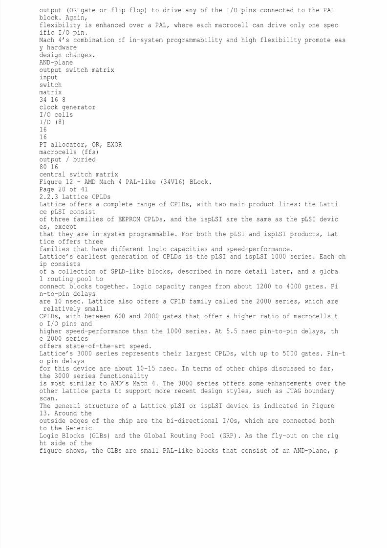
TheXC4000featuresalogicblock(calledaConfigurableLogicBlock(CLB)byXilinx)thatisbasedonlook-uptables(LUTs).ALUTisasmallonebitwidememoryarray,wheretheaddresslinesforthememoryareinputsofthelogicblockandtheonebitoutputfromthememoryistheLUToutput.ALUTwithKinputswouldthencorrespondtoa2Kx1bitmemory,andcanrealizeanylogicfunctionofitsKinputsbyprogrammingthelogicfunction’struthtabledirectlyintothememory.TheXC4000CLBcontainsthreeseparateLUTs,intheconfigurationshowninFigure18.Therearetwo4-inputLUTSthatarefedbyCLBinputs,andthethird
LUTcanbeusedincombinationwiththeothertwo.ThisarrangementallowstheCLBtoimplementawiderangeoflogicfunctionsofuptonineinputs,twoseparatefunctionsoffourinputsorotherpossibilities.EachCLBalsocontainstwoflip-flops.Figure18-XilinxXC4000ConfigurableLogicBlock(CLB).selectorInputsClockVccFG
Q1Q2ERDQSSDQERstatestate
7/31/2019 FPGA vs CPLD
http://slidepdf.com/reader/full/fpga-vs-cpld 19/27
G4G3G2G1F4F3F2F1C1C2C3C4OutputsLookupTableLookupTableLookupTablePage29of41Towardthegoalofprovidinghighdensitydevicesthatsupporttheintegrationofentiresystems,theXC4000chipshave“systemoriented”features.Forinstance,eachCLBcontainscircuitrythatallowsittoefficientlyperformarithmetic(i.e.,acircuitthatcanimplementafastcarryoperationforadder-likecircuits)andalsotheLUTsinaCLBcanbeconfigured
asread/writeRAMcells.Anewversionofthisfamily,the4000E,hastheadditionalfeaturethattheRAMcanbeconfiguredasadualportRAMwithasinglewriteandtworeadports.Inthe4000E,RAMblockscanbesynchronousRAM.Also,eachXC4000chipincludesverywideAND-planesaroundtheperipheryofthelogicblockarraytofacilitateimplementingcircuitblockssuchaswidedecoders.Besideslogic,theotherkeyfeaturethatcharacterizesanFPGAisitsinterconnectstructure.TheXC4000interconnectisarrangedinhorizontalandverticalchannels.Eachch
annelcontainssomenumberofshortwiresegmentsthatspanasingleCLB(thenumberofsegmentsineachchanneldependsonthespecificpartnumber),longersegmentsthatspantwoCLBs,andverylongsegmentsthatspantheentirelengthorwidthofthechip.Programmableswitchesareavailable(seeFigure5)toconnecttheinputsandoutputsoftheCLBstothewiresegments,ortoconnectonewiresegmenttoanother.AsmallsectionofaroutingchannelrepresentativeofanXC4000deviceappearsinFigure19.Thefigureshowsonlythewiresegmentsinahorizontalchannel,and
doesnotshowtheverticalroutingchannels,theCLBinputsandoutputs,ortheroutingswitches.AnimportantpointworthnotingabouttheXilinxinterconnectisthatsignalsmustpassthroughswitchestoreachoneCLBfromanother,andthetotalnumberofswitchestraverseddependsontheparticularsetofwiresegmentsused.Thus,speed-performanceofanimplementedcircuitdependsinpartonhowthewiresegmentsareallocatedtoindividualsignalsbyCADtools.

7/31/2019 FPGA vs CPLD
http://slidepdf.com/reader/full/fpga-vs-cpld 20/27
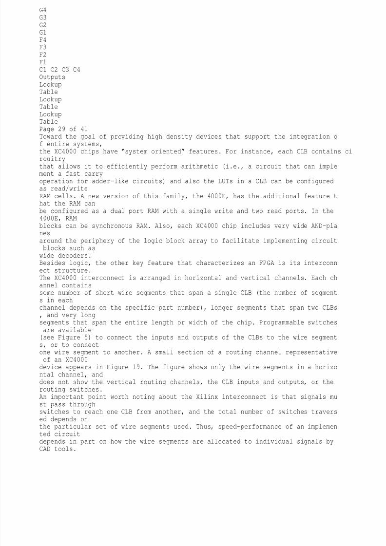
Page30of412.3.2AlteraFLEX8000andFLEX10000FPGAsAltera’sFLEX8000seriesconsistsofathree-levelhierarchymuchlikethatfoundinCPLDs.However,thelowestlevelofthehierarchyconsistsofasetoflookuptables,ratherthananSPLDlikeblock,andsotheFLEX8000iscategorizedhereasanFPGA.Itshouldbenoted,however,thatFLEX8000isacombinationofFPGAandCPLDtechnologies.FLEX8000isSRAM-basedandfeaturesafour-inputLUTasitsbasiclogicblock.Logiccapacityrangesfromabout4000gatestomorethan15,000forthe8000series.TheoverallarchitectureofFLEX8000isillustratedinFigure20.Thebasiclogicblock,calledaLogicElement(LE)containsafour-inputLUT,aflip-flop,andspecial-purposecarrycircuitryforarithmeticcircuits(similartoXilinxXC4000).TheLEalsoincludescascadecircuitrythatallowsforefficientimplementationofwideANDfunctions.DetailsoftheLEareillustratedinFigure21.IntheFLEX8000,LEsaregroupedintosetsof8,calledLogicArrayBlocks(LABs,aterm
borrowedfromAltera’sCPLDs).AsshowninFigure22,eachLABcontainslocalinterconnectandeachlocalwirecanconnectanyLEtoanyotherLEwithinthesameLAB.LocalinterconnectFigure19-XilinxXC4000WireSegments.CLBCLBCLBCLBCLBCLBCLBCLBCLBCLBlength1wireslength2wires
longwiresverticalchannelsnotshownPage31of41I/OI/OFastTrackinterconnectLAB(8LogicElements&localinterconnect)Figure20-ArchitectureofAlteraFLEX8000FPGAs.
CarryinCascadeinLEoutCascadeoutCarryoutcntrl4cntrl3cntrl2cntrl1data4
7/31/2019 FPGA vs CPLD
http://slidepdf.com/reader/full/fpga-vs-cpld 21/27
data3data2data1set/clearCarryclockLook−upTableCascadeSQDRFigure21-AlteraFLEX8000LogicElement(LE).Page32of41alsoconnectstotheFLEX8000’sglobalinterconnect,calledFastTrack.FastTrackissimilartoXilinxlonglinesinthateachFastTrackwireextendsthefullwidthorheightofthedevice.However,amajordifferencebetweenFLEX8000andXilinxchipsisthatFastTrackconsistsofonlylonglines.ThismakestheFLEX8000easyforCADtoolstoautomaticallyconfigure.AllFast-Trackwireshorizontalwiresareidentical,andsointerconnectdelaysintheFL
EX8000aremorepredictablethanFPGAsthatemploymanysmallerlengthsegmentsbecausetherearefewerprogrammableswitchesinthelongerpaths.Predictabilityisfurtheredaidedbythefactthatconnectionsbetweenhorizontalandverticallinespassthroughactivebuffers.TheFLEX8000architecturehasbeenextendedinthestate-of-the-artFLEX10000family.FLEX10000offersallofthefeaturesofFLEX8000,withtheadditionofvariable-sizedblocksofSRAM,calledEmbeddedArrayBlocks(EABs).ThisideaisillustratedinFigure23,whichshowsthateachrowinaFLEX10000chiphasanEABononeend.EachEABisconfigurab
letoserveasanSRAMblockwithavariableaspectratio:256x8,512x4,1Kx2,or2Kx1.Inaddition,anEABcanalternativelybeconfiguredtoimplementacomplexlogiccircuit,suchasamultiplier,by42cntrlcascade,carrydata4ToFastTrackLEinterconnectLELE
toadjacentLABToFastTrackinterconnectToFastTrackinterconnectFromFastTrackinterconnectlocalinterconnectFigure22-AlteraFLEX8000LogicArrayBlock(LAB).Page33of41

7/31/2019 FPGA vs CPLD
http://slidepdf.com/reader/full/fpga-vs-cpld 22/27
employingitasalargemulti-outputlookuptable.Alteraprovides,aspartoftheirCADtools,severalmacro-functionsthatimplementusefullogiccircuitsinEABs.CountingtheEABsaslogicgates,FLEX10000offersthehighestlogiccapacityofanyFPGA,althoughitishardtoprovideanaccuratenumber.2.3.3AT&TORCAFPGAsAT&T’sSRAM-basedFPGAsfeatureanoverallstructuresimilartothatinXilinxFPGAs,andiscalledOptimizedReconfigurableCellArray(ORCA).TheORCAlogicblockisbasedonLUTs,containinganarrayofProgrammableFunctionUnits(PFUs).ThestructureofaPFUisshowninFigure24.APFUpossessesauniquekindofconfigurabilityamongLUT-basedlogicblocks,inthatitcanbeconfiguredinthefollowingways:asfour4-inputLUTs,astwo5-inputLUTs,andasone6-inputLUT.Akeyelementofthisarchitectureisthatwhenusedasfour4-I/OI/OEABEAB
Figure23-ArchitectureofAlteraFLEX10KFPGAs.Page34of41inputLUTs,severaloftheLUTs’inputsmustcomefromthesamePFUinput.WhilethisreducestheapparentfunctionalityofthePFU,italsosignificantlyreducesthecostofthewiringassociatedwiththechip.ThePFUalsoincludesarithmeticcircuitry,likeXilinxXC4000andAlteraFLEX8000,andlikeXilinxXC4000aPFUcanbeconfiguredasaRAMblock.ArecentlyannouncedversionoftheORCAchipalsoallowsdual-portandsynchronousRAM.ORCA’sinterconnectstructureisalsodifferentfromthoseinotherSRAM-basedFPGAs.
EachPFUconnectstointerconnectthatisconfiguredinfour-bitbuses.Thisprovidesformoreefficientsupportfor“system-level”designs,sincebusesarecommoninsuchapplications.TheORCAfamilyhasbeenextendedintheORCA2series,andoffersveryhighlogiccapacityupto40,000logicgates.ORCA2featuresatwo-levelhierarchyofPFUsbasedontheoriginalORCAarchitecture.LUTLUTLUTLUTD
DDDQQQQswitchmatrixFigure24-AT&TProgrammableFunctionUnit(PFU).Page35of412.3.4ActelFPGAs

7/31/2019 FPGA vs CPLD
http://slidepdf.com/reader/full/fpga-vs-cpld 23/27
IncontrasttoFPGAsdescribedabove,thedevicesmanufacturedbyActelarebasedonantifusetechnology.Acteloffersthreemainfamilies:Act1,Act2,andAct3.Althoughallthreegenerationshavesimilarfeatures,thispaperwillfocusonthemostrecentdevices,sincetheyareapttobemorewidelyusedinthelongerterm.UnliketheFPGAsdescribedabove,Acteldevicesarebasedonastructuresimilartotraditionalgatearrays;thelogicblocksarearrangedinrowsandtherearehorizontalroutingchannelsbetweenadjacentrows.ThisarchitectureisillustratedinFigure25.ThelogicblocksintheActeldevicesarerelativelysmallincomparisontotheLUTbasedonesdescribedabove,andarebasedonmultiplexers.Figure26illustratesthelogicblockintheAct3andshowsthatitcomprisesanANDandORgatethatareconnectedtoamultiplexerbasedcircuitblock.Themultiplexercircuitisarrangedsuchthat,incombinationwiththetwologicgates,averywiderangeoffunctionscanberealizedinasinglelogicblock.AbouthalfofthelogicblocksinanAct3devicealsocontainaflip-flop.Figure25-StructureofActelFPGAs.
RowsBlockLogicRoutingChannelsI/OBlocksI/OBlocksI/OBlocksI/OBlocksPage36of41Asstatedabove,Actel’sinterconnectisorganizedinhorizontalroutingchannels.Thechannelsconsistofwiresegmentsofvariouslengthswithantifusestoconnectlogicbloc
kstowiresegmentsoronewiretoanother.Also,althoughnotshowninFigure25,Actelchipshaveverticalwiresthatoverlaythelogicblocks,forsignalpathsthatspanmultiplerows.Intermsofspeed-performance,itwouldseemprobablethatActelchipsarenotfullypredictable,becausethenumberofantifusestraversedbyasignaldependsonhowthewiresegmentsareallocatedduringcircuitimplementationbyCADtools.However,Actelprovidesarichselectionofwiresegmentsofdifferentlengthineachchannelandhasdevelopedalgorithmsthatguaranteestrictlimitsonthe
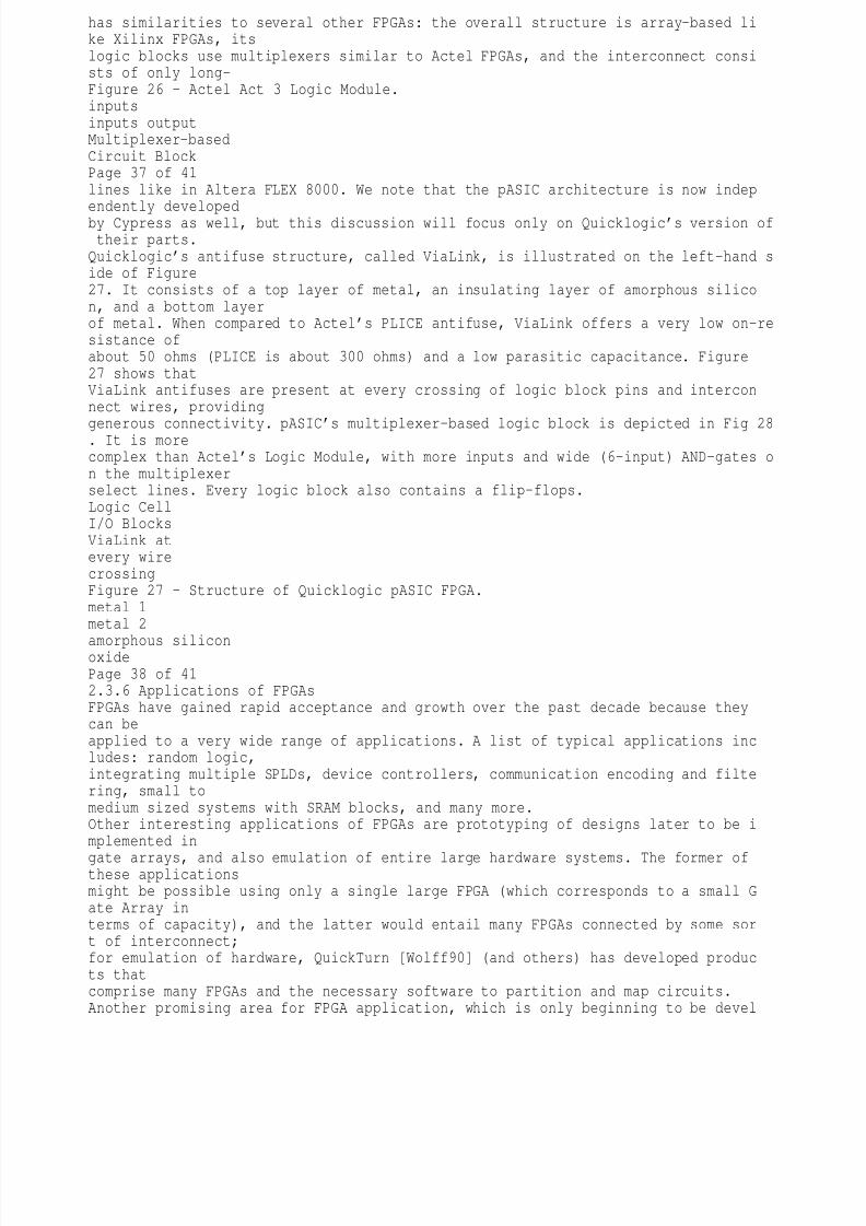
numberofantifusestraversedbyanytwo-pointconnectioninacircuitwhichimprovesspeed-performancesignificantly.2.3.5QuicklogicpASICFPGAsThemaincompetitorforActelinantifuse-basedFPGAsisQuicklogic,whosehastwofamiliesofdevices,calledpASICandpASIC-2.ThepASIC-2isanenhancedversionthathasonlyrecentlybeenintroduced,andwillnotbediscussedhere.ThepASIC,asillustratedinFigure27,
7/31/2019 FPGA vs CPLD
http://slidepdf.com/reader/full/fpga-vs-cpld 24/27
hassimilaritiestoseveralotherFPGAs:theoverallstructureisarray-basedlikeXilinxFPGAs,itslogicblocksusemultiplexerssimilartoActelFPGAs,andtheinterconnectconsistsofonlylong-Figure26-ActelAct3LogicModule.inputsinputsoutputMultiplexer−basedCircuitBlockPage37of41lineslikeinAlteraFLEX8000.WenotethatthepASICarchitectureisnowindependentlydevelopedbyCypressaswell,butthisdiscussionwillfocusonlyonQuicklogic’sversionoftheirparts.Quicklogic’santifusestructure,calledViaLink,isillustratedontheleft-handsideofFigure27.Itconsistsofatoplayerofmetal,aninsulatinglayerofamorphoussilicon,andabottomlayerofmetal.WhencomparedtoActel’sPLICEantifuse,ViaLinkoffersaverylowon-resistanceofabout50ohms(PLICEisabout300ohms)andalowparasiticcapacitance.Figure27showsthatViaLinkantifusesarepresentateverycrossingoflogicblockpinsandinterconnectwires,providing
generousconnectivity.pASIC’smultiplexer-basedlogicblockisdepictedinFig28.ItismorecomplexthanActel’sLogicModule,withmoreinputsandwide(6-input)AND-gatesonthemultiplexerselectlines.Everylogicblockalsocontainsaflip-flops.LogicCellI/OBlocksViaLinkateverywirecrossingFigure27-StructureofQuicklogicpASICFPGA.metal1metal2
amorphoussiliconoxidePage38of412.3.6ApplicationsofFPGAsFPGAshavegainedrapidacceptanceandgrowthoverthepastdecadebecausetheycanbeappliedtoaverywiderangeofapplications.Alistoftypicalapplicationsincludes:randomlogic,integratingmultipleSPLDs,devicecontrollers,communicationencodingandfiltering,smalltomediumsizedsystemswithSRAMblocks,andmanymore.OtherinterestingapplicationsofFPGAsareprototypingofdesignslatertobeimplementedin
gatearrays,andalsoemulationofentirelargehardwaresystems.TheformeroftheseapplicationsmightbepossibleusingonlyasinglelargeFPGA(whichcorrespondstoasmallGateArrayintermsofcapacity),andthelatterwouldentailmanyFPGAsconnectedbysomesortofinterconnect;foremulationofhardware,QuickTurn[Wolff90](andothers)hasdevelopedproductsthatcomprisemanyFPGAsandthenecessarysoftwaretopartitionandmapcircuits.AnotherpromisingareaforFPGAapplication,whichisonlybeginningtobedevel

7/31/2019 FPGA vs CPLD
http://slidepdf.com/reader/full/fpga-vs-cpld 25/27
oped,istheusageofFPGAsascustomcomputingmachines.Thisinvolvesusingtheprogrammablepartsto“execute”software,ratherthancompilingthesoftwareforexecutiononaregularCPU.TheQSA1A2A3A4A5A6DQB1B2C1C2D1D2E1E2F1F2F3
F4F5F6RSQCQRFZNZQZAZOZ0
10101Figure28-Quicklogic(Cypress)LogicCell.Page39of41readerisreferredtotheFPGA-BasedCustomComputingWorkshop(FCCM)heldforthelastfouryearsandpublishedbytheIEEE.ItwasmentionedinSection2.2.8thatwhendesignsaremappedintoCPLDs,piecesofthedesignoftenmapnaturallytotheSPLD-likeblocks.However,designsmappedinto
anFPGAarebrokenupintologicblock-sizedpiecesanddistributedthroughanareaoftheFPGA.DependingontheFPGA’sinterconnectstructure,theremaybevariousdelaysassociatedwiththeinterconnectionsbetweentheselogicblocks.Thus,FPGAperformanceoftendependsmoreuponhowCADtoolsmapcircuitsintothechipthanisthecaseforCPLDs.3SummaryandConclusionsWehavepresentedasurveyoffield-programmabledevices,describingthebasictechnologythat

7/31/2019 FPGA vs CPLD
http://slidepdf.com/reader/full/fpga-vs-cpld 26/27
providestheprogrammabilityandadescriptionofmanyofthearchitecturesinthecurrentmarketplace.ThispaperhasnotfocussedontheequallyimportantissueofCADtoolsforFPDs.Webelievethatovertimeprogrammablelogicwillbecomethedominantformofdigitallogicdesignandimplementation.Theireaseofaccess,principallythroughthelowcostofthedevices,makesthemattractivetosmallfirmsandsmallpartsoflargecompanies.Thefastmanufacturingturn-aroundtheyprovideisanessentialelementofsuccessinthemarket.AsarchitectureandCADtoolsimprove,thedisadvantagesofFPDscomparedtoMask-ProgrammedGateArrayswilllessen,andprogrammabledeviceswilldominate.Page40of414FurtherReadingAreasonableintroductiontoFPGAscanbefoundinthebook:[Brow92]S.Brown,R.Francis,J.Rose,Z.Vranesic,Field-ProgrammableGateArrays,KluwerAcademicPublishers,May1992.AmorespecificdiscussionofthreeFPGA/CPLDarchitecturescanbefoundin:[Trim94]S.Trimberger,Ed.,Field-ProgrammableGateArrayTechnology,KluwerAcademicPublishers,1994.
Moredetaileddiscussionofarchitecturaltrade-offscanbefoundin:[Rose93]J.Rose,A.ElGamal,A.Sangiovanni-Vincentelli,“ArchitectureofField-ProgrammableGateArrays,”inProceedingsoftheIEEE,Vol.81,No.7,July1993,pp.1013-1029.Atextbook-liketreatment,includingdigitallogicdesignbasedontheXilinx3000seriesandtheAlgotronixCALchipcanbefoundin:[Oldf95]J.Oldfield,R.Dorf,FieldProgrammableGateArrays,JohnWiley&Sons,NewYork,1995.Uptodateresearchtopicscanbefoundinseveralconferences-CICC,ICCAD,DACandthepublishedproceedings:FPGASymposiumSeries:FPGA‘95:The3rdInt’lACMSymposium
onField-ProgrammableGateArrays,andFPGA‘96.Inaddition,therehavebeeninternationalworkshopsonField-ProgrammableLogicinOxford(1991),Vienna(1992),Oxford(1993)Prague(1994),andOxford(1995)andDarmstadt(1996),someoftheproceedingsofwhicharepublishedbyAbingdonPress,UK.Finally,thereistheCanadianWorkshoponFieldProgrammableDevices,1994,1995,and1996.5References[Birk92]J.Birkneretal,“Avery-high-speedfield-programmablegatearrayusingmetal-tometalantifuseprogrammableelements,”MicroelectronicsJournal,v.23,pp.561-568.
[Ham88]E.Hamdyetal,“Dielectric-basedantifuseforlogicandmemoryICs,”IEEEInternationalElectronDevicesMeetingTechnicalDigest,pp.786-789,1988.[Marp94]DavidMarpleandLarryCooke,“ProgrammingAntifusesinCrossPoint’sFPGA,”Proc.CICC94,May1994,pp.185-188.[MAX94]AlteraCorporation,“MAX+PlusIICADDesignSystem,version5.0”,1994.[ORCA94]AT&TCorp.,“ORCA2CSeriesFPGAs,PreliminaryDataSheets,”April1994.Page41of41[Wolff90]H.Wolff,“HowQuickTurnisfillingthegap,”Electronics,April1990.AcknowledgmentsWewishtoacknowledgestudents,colleagues,andacquaintancesinindustrywhoh

7/31/2019 FPGA vs CPLD
http://slidepdf.com/reader/full/fpga-vs-cpld 27/27
avehelpedcontributetoourknowledge.