Designing of a AMBA-AHB Multilayer Bus matrix SelfMotivated Arbitration scheme
International Journal of Science and Research (IJSR) ISSN (Online): 2319-7064
Index Copernicus Value (2013): 6.14 | Impact Factor (2015): 6.391
Volume 5 Issue 5, May 2016
www.ijsr.net Licensed Under Creative Commons Attribution CC BY
FPGA Implementation of AHB to APB Protocol
Sowmya Aithal1, Dr. J. S. Baligar
2, Guruprasad S. P.
3
1PG Student, Dr. Ambedkar Institute of Technology, Bangalore, India
2Associate Professor, Dept. of ECE, Dr. Ambedkar Institute of Technology, Bangalore, India
3Senior Design Engineer, Certitude TechnologiesPrivate Limited, Bangalore, India
Abstract:The field of technology is evolving at a very fast pace. The competition is very intense. So the need of the hour is to produce
efficient system. In accomplishing this objective we are required to establish better interaction among all the components of the system.
This requirement is fulfilled by the Advanced Microcontroller Bus Architecture (AMBA) protocol from Advanced RISC Machines
(ARM).The AMBA is the on-chip standard for the communication among components in Application Specific Integrated Circuits
(ASIC) or System on Chip (SoC). This paper focuses on the 2 protocols of AMBA which are Advanced High Performance Bus (AHB)
and Advanced Peripheral Bus (APB) and theAPB bridge. The coding is done in Verilog synthesis on Xilinx 14.7 ISE and simulation on
ISim simulator and FPGA implementation on Spartan 3.
Keywords: AMBA; APB bridge, AHB, APB, IP, SoC, Verilog ,VLSI
1. Introduction
The miniaturization in the technology is leading to the
emphasizing on the communication among the modules of
the System on Chip (SoC). The SoC is the integration of all
the components required onto the same chip so called
System on Chip. The interaction between these components
of the system is critical for every SoC. The
intercommunication is maintained by AMBA protocol. The
AMBA protocol provides an efficient way for the interaction
and increases the performance of the system.
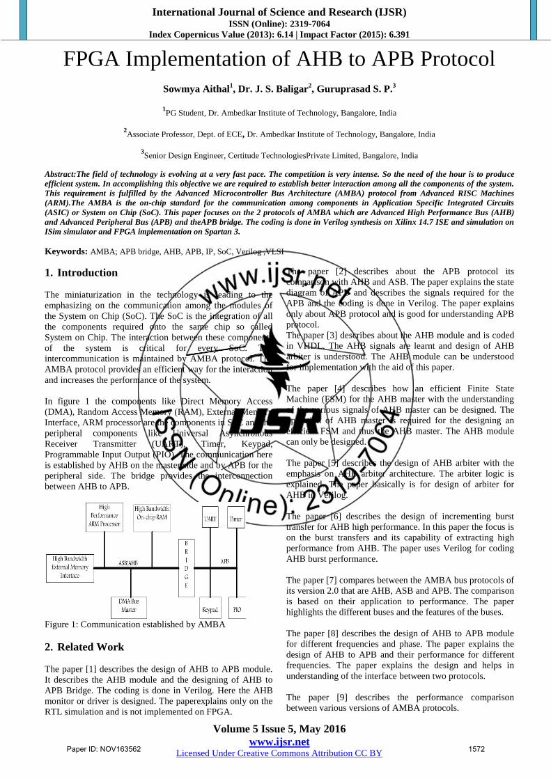
In figure 1 the components like Direct Memory Access
(DMA), Random Access Memory (RAM), External Memory
Interface, ARM processor are the components in SoC and the
peripheral components like Universal Asynchronous
Receiver Transmitter (UART), Timer, Keypad,
Programmable Input Output (PIO). The communication here
is established by AHB on the master side and by APB for the
peripheral side. The bridge provides the interconnection
between AHB to APB.
Figure 1: Communication established by AMBA
2. Related Work
The paper [1] describes the design of AHB to APB module.
It describes the AHB module and the designing of AHB to
APB Bridge. The coding is done in Verilog. Here the AHB
monitor or driver is designed. The paperexplains only on the
RTL simulation and is not implemented on FPGA.
The paper [2] describes about the APB protocol its
comparison with AHB and ASB. The paper explains the state
diagram of APB and describes the signals required for the
APB and the coding is done in Verilog. The paper explains
only about APB protocol and is good for understanding APB
protocol.
The paper [3] describes about the AHB module and is coded
in VHDL. The AHB signals are learnt and design of AHB
arbiter is understood. The AHB module can be understood
for implementation with the aid of this paper.
The paper [4] describes how an efficient Finite State
Machine (FSM) for the AHB master with the understanding
of the various signals of AHB master can be designed. The
operation of AHB master is required for the designing an
efficient FSM and thus the AHB master. The AHB module
can only be designed.
The paper [5] describes the design of AHB arbiter with the
emphasis on AHB arbiter architecture. The arbiter logic is
explained. The paper basically is for design of arbiter for
AHB in Verilog.
The paper [6] describes the design of incrementing burst
transfer for AHB high performance. In this paper the focus is
on the burst transfers and its capability of extracting high
performance from AHB. The paper uses Verilog for coding
AHB burst performance.
The paper [7] compares between the AMBA bus protocols of
its version 2.0 that are AHB, ASB and APB. The comparison
is based on their application to performance. The paper
highlights the different buses and the features of the buses.
The paper [8] describes the design of AHB to APB module
for different frequencies and phase. The paper explains the
design of AHB to APB and their performance for different
frequencies. The paper explains the design and helps in
understanding of the interface between two protocols.
The paper [9] describes the performance comparison
between various versions of AMBA protocols.
Paper ID: NOV163562 1572
International Journal of Science and Research (IJSR) ISSN (Online): 2319-7064
Index Copernicus Value (2013): 6.14 | Impact Factor (2015): 6.391
Volume 5 Issue 5, May 2016
www.ijsr.net Licensed Under Creative Commons Attribution CC BY
he paper [10] describes the methodology for AHB master
wrappers for its use in Intellectual Property (IP) cores.
3. AHB Bus Protocol
The AHB is the high performance bus and synthesizable
designs.It supports burst transfers, split transactions, non-
tristate implementation. The burst transfers is the block of
data which is sent at a fast pace. The block of data can vary
from 8 to 16 beat bursts. The split transfers referred to option
for splitting the beat bursts into smaller beats and
transferring. The non tristate implementation is not including
high impedance state. Every transfer consists of an address
and control cycle, one or more cycles for the data. The AHB
bus master has signals for writing, data buses, address buses,
burst transfers, etc. The AHB bus master when ready for the
transfer will check if peripheral device is ready for the
transfer if ready then the transaction takes place. The reverse
operation occurs when read transfer happens.The AHB
controller controls the transaction between AHB master and
APB peripheral.
4. APB Bus Protocol
The APB protocol is the bus protocol employed for the
peripherals like UART, Keypad, PIO, Timer, LCD Display
or LED display etc to name a few.
The APB protocol is low performance low power bus
protocol. It is basically used for peripherals as the name
suggests. The APB protocol has low bandwidth.
The APB peripherals as listed can be enabled based on their
enable signals and the transaction can be accomplished.
The APB peripherals in this work is enabled based on the
address and so is fast and efficient.
5. AHB to APB Module
The AHB to APB module consists of the AHB signals and
APB signals included to form the controller part and the
peripherals which include 6 of the slaves.
The AHB to APB module is coded in Verilog and
synthesized in Xilinx 14.7 ISE and simulated using ISIM
simulator which is inbuilt in Xilinx 14.7.
The AHB to APB module can be implemented on Spartan 3
FPGA and usingChipscope can be verified. The higher
Spartan series also is compatible and the AHB to APB
module can be dumped onto it.
6. Results
The synthesis results are shown along with the simulation
results.
1) Minimum period: 5.018ns
2) Maximum Frequency: 199.299MHz
3) Minimum input arrival time before clock: 6.429ns
4) Maximum output required time after clock: 14.120ns
5) Maximum combinational path delay: 8.525ns
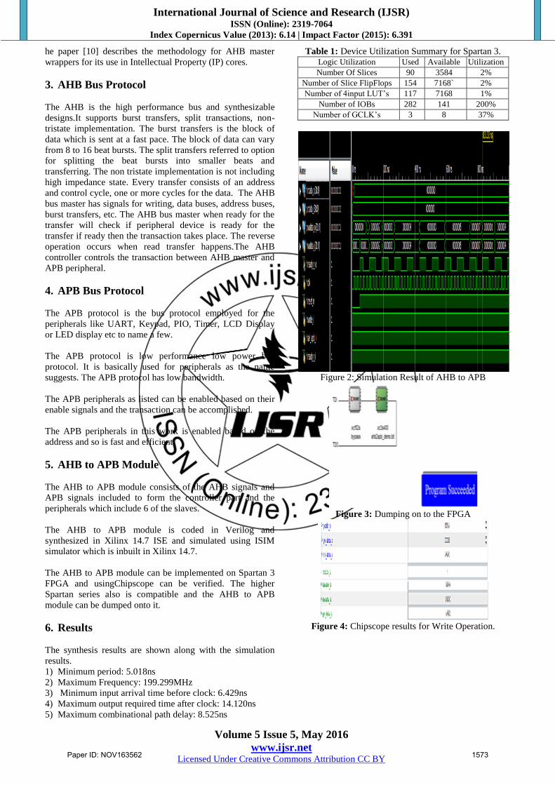
Table 1: Device Utilization Summary for Spartan 3. Logic Utilization Used Available Utilization
Number Of Slices 90 3584 2%
Number of Slice FlipFlops 154 7168` 2%
Number of 4input LUT’s 117 7168 1%
Number of IOBs 282 141 200%
Number of GCLK’s 3 8 37%
Figure 2: Simulation Result of AHB to APB
Figure 3: Dumping on to the FPGA
Figure 4: Chipscope results for Write Operation.
Paper ID: NOV163562 1573
International Journal of Science and Research (IJSR) ISSN (Online): 2319-7064
Index Copernicus Value (2013): 6.14 | Impact Factor (2015): 6.391
Volume 5 Issue 5, May 2016
www.ijsr.net Licensed Under Creative Commons Attribution CC BY
Figure 4: Chipscope results for Read Operation.
The figures 2, 3, 4, 5 show the simulation results, with
remaining figures illustrating the dumping onto FPGA and
the Chipscope results or both write and read operations.
The table 1 shows the device utilization for Spartan 3 FPGA
and it shows the utilization of resources to the minimal. The
Chipscope results verify the design.
7. Conclusion and Future Work
The AHB to APB module is synthesized, simulated and
verified by dumping onto the Spartan 3 FPGA. The
Chipscope results for both write and read operations are
verified. The area, time consumed by the design is low and
so we can conclude as a very effective design.
The AHB to APB module can be dumped onto any other
Spartan Series Kits also for similar verification
The design of the interface between AHB and APB can be
extended into other versions of the AMBA protocol like
ASB, AXI to name a few.
The implementation of interface between other protocols of
AMBA with APB is the future work.
References
[1] Design of AMBA Based AHB2APB Bridge by
Vani.R.M andM.Roopain IJCSNS International Journal
of Computer Science and Network Security, 2010.
[2] Design & Implementation of Advance Peripheral Bus
Protocol by Heli Shah, ChinmayModi, BhargavTarpara
in International Journal of Scientific Engineering and
Applied Science (IJSEAS),2015.
[3] Implementation of AMBA AHB protocol for high
capacity memory management using VHDL by
Varshavishwarkama,Abhishekchoubey,ArvindSahu in
International Journal on Computer Science and
Engineering (IJCSE),2012.
[4] Design of an Efficient FSM for an Implementation of
AMBA AHB Master by Pravin S. Shete,Dr. ShrutiOza,
in International Journal of Advanced Research in
Computer Science and Software Engineering, 2014.
[5] Study Of High Performance AmbaAhb Reconfigurable
Arbiter For On-Chip Bus Architecture by Pravin S.
Shete,Dr. ShrutiOza, International Journal of Electrical,
Electronics and Data Communication, 2014.
[6] Design Incrementing Burst Data Transfer Operation for
AMBA-Advanced High Performance Bus by
MitalMungra and Assi. Prof. Vishal S.Vora in
International Journal of Emerging Trends in Electrical
and Electronics (IJETEE), 2013.
[7] An Overview of Advanced Microcontroller Bus
Architecture relate on APB bridge by RadhikaKoti,
DivyaMeshram in International Journal of Scientific and
Research Publications, 2013.
[8] Design of AHB2APB Bridge for different phase and
Frequency by Vani.R.M andM.Roopa in International
Journal of Computer and Electrical Engineering, 2011.
[9] Performance Comparison of AMBA Bus-Based System-
On-Chip Communication Protocol by
AnuragShrivastava G.S. Tomar, Ashutosh Kumar Singh
in International Conference on Communication Systems
and Network Technologies, 2011.
[10] A methodology for the design of AHB bus master
wrappers by Marc Bertola, Guy Bois in IEEE ,2003.
[11] AMBA Specifications from ARM.
Paper ID: NOV163562 1574


![Design and Implementation of Efficient FSM for AHB Master and … · 2017-07-22 · [1] AMBA specification, version 2.0 [2] “AHB Example AMBA System”, Technical Reference Manual,](https://static.fdocuments.in/doc/165x107/5e8ff8e85e980155c60fde82/design-and-implementation-of-efficient-fsm-for-ahb-master-and-2017-07-22-1-amba.jpg)