FPGA-Based Data Acquistion System for Ultrasound...
76
FPGA-Based Data Acquistion System for Ultrasound Tomography Michael Aitken A project report submitted to the Department of Electrical Engineering, University of Cape Town, in partial fulfilment of the requirements for the degree of Bachelor of Science in Engineering. Cape Town, October 2006
Transcript of FPGA-Based Data Acquistion System for Ultrasound...
FPGA-Based Data Acquistion Systemfor Ultrasound Tomography
Michael Aitken
A project report submitted to the Department of Electrical Engineering,
University of Cape Town, in partial fulfilment of the requirements for the
degree of Bachelor of Science in Engineering.
Cape Town, October 2006

Declaration
I declare that this project report is my own, unaided work. It is being submitted for thedegree of Bachelor of Science in Engineering at the University of Cape Town. It has notbeen submitted before for any degree or examination in any other university.
Signature of Author . . . . . . . . . . . . . . . . . . . . . . . . . . . . . . . . . . . . . . . . . . . . . . . . . . . . . . . . . . . . . .
Cape Town
22 October 2006
i

Abstract
Ultrasound Tomography involves the acquisition and analysis of large amounts of data,both of which must be done at high speed in order to be implemented in a mobile prod-uct. FPGA technology promises to provide the necessary parallel processing capabilitiesin order to accomplish various strenuous processing procedures. At the same time thetechnology allows a system to be designed and prototyped quickly and cost-effectively.
However, an FPGA device is limited by the speed at which it can acquire raw data. Tofacilitate ultrasound tomography, the external circuitry is responsible for acquiring highresolution data at high speeds that are sufficient in order to allow effective signal pro-cessing. The circuitry must also perform the opposite function, that being the ability totransform high resolution digital data into analogue signals at high speed.
This thesis sets out to investigate the recent developments in FPGA technology, lookingspecifically at the benefits that FPGAs deliver to embedded system design. It then moveson to suggest a software/hardware configuration that will provide a cheap, fast-trackedworking demonstration of an ultrasound tomography system. It takes the reader throughthe process of building the entire system:
• designing and implementing the external hardware
• creating a customized soft-core Nios II processor
• interfacing all the system components
• writing the control code
• testing the system
• demonstrating valid results.
Lastly, and most importantly, since this project merely lays the foundation for furtherexploring FPGA technology, a range of possible project extensions are suggested.
ii

This thesis is dedicated to my parents, who, even from so far away, gave me the love andsupport to get me this far.
I owe them more then can be imagined.
iii

Acknowledgements
I would like to sincerely thank Dr A.J. Wilkinson for his proposal, his time, and hisknowledgeable advice on this project. Thanks also go to Mr S. Ginsberg for his helpin producing the PCB. Lastly, a thank you to my fellow lab mates for the jokes, thedistractions, the good times, and the encouragement to work hard inbetween.
iv
Contents
Declaration i
Abstract ii
Acknowledgements iv
Nomenclature xi
1 Introduction 1
1.1 Objectives . . . . . . . . . . . . . . . . . . . . . . . . . . . . . . . . . . 1
1.2 Assumptions . . . . . . . . . . . . . . . . . . . . . . . . . . . . . . . . 2
1.3 Sources of Information . . . . . . . . . . . . . . . . . . . . . . . . . . . 2
1.4 Limitations of Research . . . . . . . . . . . . . . . . . . . . . . . . . . . 2
1.5 Plan of Development . . . . . . . . . . . . . . . . . . . . . . . . . . . . 3
2 Embedded System Design using FPGA Technology 4
2.1 Introduction to FPGAs . . . . . . . . . . . . . . . . . . . . . . . . . . . 4
2.2 ASIC vs FPGA as a design choice . . . . . . . . . . . . . . . . . . . . . 6
2.3 Parallel Processing . . . . . . . . . . . . . . . . . . . . . . . . . . . . . 6
2.4 System-On-a-Chip Design . . . . . . . . . . . . . . . . . . . . . . . . . 7
2.5 Fast Reconfigurability . . . . . . . . . . . . . . . . . . . . . . . . . . . . 8
3 Ultrasound Tomography 10
3.1 Overview . . . . . . . . . . . . . . . . . . . . . . . . . . . . . . . . . . 10
3.2 Time-Of-Flight Theory . . . . . . . . . . . . . . . . . . . . . . . . . . . 10
3.3 Ultrasound Transducers . . . . . . . . . . . . . . . . . . . . . . . . . . . 11
3.4 Tomographical Ring Configuration . . . . . . . . . . . . . . . . . . . . . 12
4 Defining the Hardware/Software Configuration 13
4.1 Objectives . . . . . . . . . . . . . . . . . . . . . . . . . . . . . . . . . . 13
4.2 System Overview . . . . . . . . . . . . . . . . . . . . . . . . . . . . . . 14
v

4.3 Hardware Breakdown . . . . . . . . . . . . . . . . . . . . . . . . . . . . 16
4.3.1 Mechanical Structure . . . . . . . . . . . . . . . . . . . . . . . . 16
4.3.2 Transducer Interface . . . . . . . . . . . . . . . . . . . . . . . . 16
4.3.3 MUX/DEMUX . . . . . . . . . . . . . . . . . . . . . . . . . . . 16
4.3.4 Amplifiers . . . . . . . . . . . . . . . . . . . . . . . . . . . . . 17
4.3.5 Digital-to-Analogue Converter . . . . . . . . . . . . . . . . . . . 17
4.3.6 Analogue-to-Digital Converter . . . . . . . . . . . . . . . . . . . 17
4.3.7 Logical Interface . . . . . . . . . . . . . . . . . . . . . . . . . . 17
4.3.8 Soft-core Processor . . . . . . . . . . . . . . . . . . . . . . . . . 17
4.3.9 DSP Hardware . . . . . . . . . . . . . . . . . . . . . . . . . . . 17
4.4 Software Breakdown . . . . . . . . . . . . . . . . . . . . . . . . . . . . 17
4.4.1 Control Software . . . . . . . . . . . . . . . . . . . . . . . . . . 18
4.4.2 Data Repository . . . . . . . . . . . . . . . . . . . . . . . . . . 18
4.4.3 Digital Signal Processing . . . . . . . . . . . . . . . . . . . . . 18
4.4.4 Graphing Tools . . . . . . . . . . . . . . . . . . . . . . . . . . . 18
5 Hardware Implementation 19
5.1 Sensory Equipment . . . . . . . . . . . . . . . . . . . . . . . . . . . . . 19
5.2 Mechanical Stand . . . . . . . . . . . . . . . . . . . . . . . . . . . . . . 20
5.3 Peripheral Board - Signal Generation Circuit . . . . . . . . . . . . . . . . 20
5.3.1 Digital to Analogue Converter . . . . . . . . . . . . . . . . . . . 20
5.3.2 Amplifier . . . . . . . . . . . . . . . . . . . . . . . . . . . . . . 21
5.3.3 Demultiplexer . . . . . . . . . . . . . . . . . . . . . . . . . . . . 22
5.4 Peripheral Board - Signal Capture Circuit . . . . . . . . . . . . . . . . . 22
5.4.1 Programmable Gain Amplifier . . . . . . . . . . . . . . . . . . . 22
5.4.2 Analogue to Digital Converter . . . . . . . . . . . . . . . . . . . 23
5.5 Peripheral Board - Power Supplies . . . . . . . . . . . . . . . . . . . . . 23
5.6 Peripheral Board - Voltage Shifters . . . . . . . . . . . . . . . . . . . . . 23
5.7 Peripheral Board - Board Fabrication . . . . . . . . . . . . . . . . . . . . 24
5.8 FPGA Kit and Peripheral Board Interface . . . . . . . . . . . . . . . . . 24
5.9 Nios II Evaluation Kit . . . . . . . . . . . . . . . . . . . . . . . . . . . . 26
5.10 Nios II Soft-core Processor & Peripherals . . . . . . . . . . . . . . . . . 26
5.10.1 Overview . . . . . . . . . . . . . . . . . . . . . . . . . . . . . . 26
5.10.2 Configuration using SoPC Builder . . . . . . . . . . . . . . . . . 27
5.10.3 PIO Interface . . . . . . . . . . . . . . . . . . . . . . . . . . . . 28
5.10.4 SPI Interface . . . . . . . . . . . . . . . . . . . . . . . . . . . . 28
5.10.5 Cyclone Pin-out Interface . . . . . . . . . . . . . . . . . . . . . 29
vi
6 Software Implementation 31
6.1 Hardware Abstraction Layer . . . . . . . . . . . . . . . . . . . . . . . . 31
6.2 Control Code . . . . . . . . . . . . . . . . . . . . . . . . . . . . . . . . 32
6.2.1 Overview . . . . . . . . . . . . . . . . . . . . . . . . . . . . . . 32
6.2.2 Synthesized Sine Wave Generation . . . . . . . . . . . . . . . . 35
6.2.3 Wave Capture . . . . . . . . . . . . . . . . . . . . . . . . . . . . 35
6.3 GDB Server . . . . . . . . . . . . . . . . . . . . . . . . . . . . . . . . . 36
6.4 Data Processing in Matlab . . . . . . . . . . . . . . . . . . . . . . . . . 37
6.4.1 Finding the TOF Value . . . . . . . . . . . . . . . . . . . . . . . 37
6.4.2 TOF Example Set . . . . . . . . . . . . . . . . . . . . . . . . . . 39
7 Test Results 43
8 Conclusions 49
9 Recommendations and Proposals 50
A Peripheral Board Schematic 52
B Peripheral Board Assembly 54
C Software Source Code 56
D Matlab Functions 61
D.1 readBin.m . . . . . . . . . . . . . . . . . . . . . . . . . . . . . . . . . . 61
D.2 extractSampling.m . . . . . . . . . . . . . . . . . . . . . . . . . . . . . 61
D.3 findTOF.m . . . . . . . . . . . . . . . . . . . . . . . . . . . . . . . . . . 62
E Photograph of the final system 63
Bibliography 64
vii

List of Figures
2.1 An FPGA logic element, courtesy of [1] . . . . . . . . . . . . . . . . . . 4
2.2 Structure of a Xilinx XC4000 FPGA, courtesy of [4] . . . . . . . . . . . 5
2.3 An example of FPGA parallelism . . . . . . . . . . . . . . . . . . . . . . 7
2.4 A System-on-a-chip configuration using an FPGA with on-chip RAM . . 8
3.1 Simple demonstration of the TOF effect . . . . . . . . . . . . . . . . . . 11
3.2 Tomograhical Ring Configuration, showing the flight paths between trans-ducers . . . . . . . . . . . . . . . . . . . . . . . . . . . . . . . . . . . . 12
4.1 Conceptualized System Overview . . . . . . . . . . . . . . . . . . . . . 15
5.1 A transducer and its connector . . . . . . . . . . . . . . . . . . . . . . . 19
5.2 Photographs of transducer array structure . . . . . . . . . . . . . . . . . 20
5.3 Schematic of Signal Generation Circuit . . . . . . . . . . . . . . . . . . 21
5.4 Schematic of Signal Generation Circuit . . . . . . . . . . . . . . . . . . 22
5.5 Schematic of the Voltage Regulators . . . . . . . . . . . . . . . . . . . . 23
5.6 The assembled peripheral board . . . . . . . . . . . . . . . . . . . . . . 25
5.7 Nios II Evaluation Kit Interfaced with the custom made peripheral board . 25
5.8 Basic Layout of Nios II Evaluation Kit, courtesy of [13] . . . . . . . . . 26
5.9 Configuration of the Nios II processor and it’s peripherals . . . . . . . . . 27
5.10 The Nios II HDL block configured with the corresponding pins . . . . . . 28
5.11 Cyclone 1C12 Functional Pin-out, courtesy of [13] . . . . . . . . . . . . 30
6.1 The HAL fitted into the project software model . . . . . . . . . . . . . . 32
6.2 Flow chart of main control software . . . . . . . . . . . . . . . . . . . . 33
6.3 Flow chart of scanning algorithm . . . . . . . . . . . . . . . . . . . . . . 34
6.4 Pseudo code for generating a sine wave table . . . . . . . . . . . . . . . 35
6.5 Generated sin wave values ready for transmission . . . . . . . . . . . . . 36
6.6 Overview of procedure used to extract TOF values . . . . . . . . . . . . 38
6.7 Original Sample Signal . . . . . . . . . . . . . . . . . . . . . . . . . . . 40
6.8 Sample set in the frequency domain . . . . . . . . . . . . . . . . . . . . 40
viii

6.9 Sample set in frequency domain with zero-ed DC and negative frequencies 40
6.10 Sample set envelope . . . . . . . . . . . . . . . . . . . . . . . . . . . . . 41
6.11 Sample set envelope with smoothing applied . . . . . . . . . . . . . . . . 41
6.12 Sample set with threshold and TOF determined . . . . . . . . . . . . . . 42
7.1 The numbering applied to the transducer transmitter/receiver pairs. (eachnumber corresponds to a transmitter and a receiver) . . . . . . . . . . . . 43
7.2 Photograph of Red Bottle under test scenario . . . . . . . . . . . . . . . 44
7.3 Photograph of Wooden Pole under test scenario . . . . . . . . . . . . . . 44
7.4 Test Subject: Empty space - raw sampled signals . . . . . . . . . . . . . 45
7.5 Test Subject: Red Bottle - raw sampled signals . . . . . . . . . . . . . . 46
7.6 Test Subject: Wooden Pole - raw sampled signals . . . . . . . . . . . . . 46
7.7 Test Subject: Empty space - surface plot of TOF values . . . . . . . . . . 47
7.8 Test Subject: Red Bottle - surface plot of TOF values . . . . . . . . . . . 47
7.9 Test Subject: Wooden Pole - surface plot of TOF values . . . . . . . . . . 48
9.1 Proposed signal generation and DSP core configuration . . . . . . . . . . 51
ix

List of Tables
2.1 ASIC Devices vs. FPGA Devices . . . . . . . . . . . . . . . . . . . . . . 6
5.1 DAC904 Specifications . . . . . . . . . . . . . . . . . . . . . . . . . . . 20
5.2 ADS802 Specifications . . . . . . . . . . . . . . . . . . . . . . . . . . . 23
5.3 The different PIO cores and their functions . . . . . . . . . . . . . . . . . 29
x

Nomenclature
ADC—Analogue to Digital Converter
AI—Artificial Intelligence
ALU—Arithmetic Logic Unit
ASIC—Application Specific Intergrated Circuit
CAD—Computer Aided Design
DAC—Digital to Analogue Converter
DSP—Digital Signal Processing
footprint—the size or area or amount of memory/chip space that a component takes up.
FPGA—Field Progammable Gate Array
GDB—GNU Debugger
HDL—Hardware Description Layer
IDE—Intergrated Development Environment, a set of graphical user interface tools thatallow the developing of code, along with debugging and version control.
JTAG—Joint Task Action Group, a standard specifying a mechanism to test and debugembedded systems and intergrated circuits
LUT—Look-Up Table
Matlab—A numerical computing environment that consists of tools for manipulating andvisualizing data.
NRE—Non-Recurring Engineering, generally refers to the once-off development workfor a product or system.
PGA—Programmable Gain Amplifier
RAM—Random Access Memory
SoC—System-On-a-Chip
SoPC—System-on-a-Programmable-Chip
TOF—Time Of Flight
xi

Chapter 1
Introduction
This thesis describes the research work, design and the implementation of a FPGA-basedData Acquisition system. The application for this system is Ultrasound Tomography,however the purpose of the project was to gain an understanding of FPGA technologyand implement a data acquisition system that would form a foundation for further researchand practice into this form of embedded system design. Therefore, this thesis does notfocus on the theory or practical nature of acoustic tomography but rather on the rapiddevelopment of a high speed data acquisition engine using relatively cheap FPGA basedtools. Such a system has far reaching uses in other fields besides tomography, such assoftware radio, radar, image processing and any other application that relies on specific,high speed, mobile processing capabilites.
In order to fully understand the functionality of FPGA technology, this thesis takes alook at the aspects of this rapidly accelerating area of electronics. The bulk of the thesisdescribes the process of designing and building a data acquisition system to perform basicultrasound scanning. Whilst this project does indeed demonstrate the speed at whichsystems can be implemented and tested using FPGA devices, it does not fully exploit theprocessing capabilities of the device. It is the natural goal of this system to allow real-time digital signal processing to take place, and this is left for further investigation andresearch in the future.
1.1 Objectives
The objectives of this thesis are the following:
• To provide a literature review of embedded system design using FPGA technology
• To provide a short introduction into ultrasound tomography
• To describe in detail the configuration of a data acquisition system for ultrasoundtomography
1
• To present the results from testing the system.
• To draw conclusions on the results and suggest future improvements and extensions
1.2 Assumptions
This project covers a wide range of content that involves various fields, including systemsengineering, software design, circuit design in CAD, component assembly, digital signalprocessing and acoustics. Thus, in order to not get overly verbose in the discussion ofwhat has been accomplished, this thesis report assumes that the reader has an understand-ing of all of the above fields.
1.3 Sources of Information
The bulk of the information acquired in this project was obtained from Internet sources.Please see the in-text numbered references and the corresponding bibliography. Any otherinformation contained here was obtained from discussions with those mentioned in theacknowledgements.
1.4 Limitations of Research
This scope of the project was limited mainly by the lack of:
• an FPGA development kit
– An evaluation version was used instead which has intentionally limited andrestricted functionality.
• licenses
– for IP/TCP code for the kit’s on-board ethernet hardware (which would haveextended the project, had there been time)
• time
– for further exploiting the capabilities of the FPGA device using digital signalprocessing, and to fine tune the implemented system.
2

1.5 Plan of Development
The following chapters in this thesis are divided up as follows:
• Chapter 2 surveys the concept of designing embedded systems using FPGA tech-nology and the benefits it can bring to processing power and general development.
• Chapter 3 discusses the basics of ultrasound tomography and describes a sensorconfiguration that is used later in the implementation.
• Chapter 4 defines the hardware and software requirements for building an ultra-sound tomography scanner using a FPGA device.
• Chapter 5 describes the final implementation of all the hardware related componentsof the system.
• Chapter 6 describes the final implementation of all the software related componentsof the system.
• Chapter 7 presents the results produced by the implemented ultrasound system aftertesting it.
• Chapter 8 discusses the results in light of the work done and draws conclusionsabout the implemented system.
• Chapter 9 provides proposals for project extensions and future work on the same orsimilar topics.
3

Chapter 2
Embedded System Design using FPGATechnology
This chapter provides a brief literature review of the past, present and future of FPGAtechnology. The purpose of understanding the basics of FPGAs is to acquire a betterappreciation of the benefits that they bring to embedded systems design.
2.1 Introduction to FPGAs
FPGA is the acronym for Field-Programmable Gate Array. The term is most commonlyapplied to electronic devices which contain an array of identical logic elements which canbe configured using a programming procedure to replicate any particular logic circuit.A normal FPGA device is usually contained within a single silicon package which mayalso house some form of memory elements[1]. A normal FPGA contains upwards of onethousand of these logic elements.
Figure 2.1: An FPGA logic element, courtesy of [1]
As shown by the example in figure 2.1, a logic element has a programmable Look-Up Ta-ble and a register (the flip-flop). The LUT can perform any logic function on the availableinputs to produce a single logic output. The final output is either this new value or theprevious value (stored in the flip-flop). Although the logic element may have more thanthe four inputs shown here, they generally only have one output. Figure 2.2 demonstratesthe way in which logic blocks are laid out to form an array inside the FPGA. Different
4

Manufactures will have slightly different configurations but all use some type of pro-grammable switch matrix at the crossing point of the logic block interconnection lines.By having programmable switches and programmable logic elements, the system can be
Figure 2.2: Structure of a Xilinx XC4000 FPGA, courtesy of [4]
configured to mimic any combination of logic functions as long as the overall design canbe fitted into the available number of logic elements and switches. The process of routinga logic function into the FPGA is, of course, a highly complex process which is usuallyspecially carried out by proprietary CAD tools designed specifically for a manufacturer’sFPGA device. In general these tools allow HDL code to be imported and representedas functional blocks which are then schematically joined together and logically linked tothe device’s I/O pins. A hardware image is then compiled and produced using advancedAI placement routines. These routines take into account the propagational effects of linelength, as well as hardware footprint and the compilation process can generally be finedtuned to the needs of the designer. This can be useful when weighing up design timevs required system footprint/speed, as a smaller faster image will take much longer tocompile, delaying the design process.
5

2.2 ASIC vs FPGA as a design choice
ASIC technology (Application-Specific Integrated Circuit) has enjoyed much success inthe past owing to it’s ability to allow for customized, high speed, efficient circuitry. Theprocess of designing, testing and setting up fabrication facilities for the production of anASIC is generally very expensive. In situations where the market for a certain deviceis large and reprogrammability is not needed, this high non-recurring engineering (NRE)cost can be countered by the smaller, faster and cheaper end product that ASIC technologyproduces. Strictly speaking, a working FPGA device programmed with a hardware imageis in fact a type of ASIC, however the FPGA’s reprogrammability makes it very differentas a design choice . The advantages and disadvantages of both types of technology aresummed up in table 2.1
ASIC FPGANRE Cost High LowUnit Cost Less Expensive More Expensive
Speed Faster SlowerRe-Configurable in the field No Yes
Footprint Smaller LargerTime to Market Longer Shorter
Cost of Debugging High Low
Table 2.1: ASIC Devices vs. FPGA Devices
2.3 Parallel Processing
Of the many advantages that FPGA devices offer, the ability to allow for customized par-allel processing is perhaps the most beneficial of all. Since a designer no longer needs torely on a ASIC vendor to provide him with the processing tools that he needs, the designercan quickly create his own processing blocks in hardware. This is hugely beneficial forcomputationally strenuous tasks, and since the cost of trial and error designing is nowessentially nil, the designer is free to experiment with different processing configurationsto fine tune his system. The basic concept is demonstrated in figure 2.3. The figure showshow an FPGA can be used to quadruple the speed of digital processing using an existingHDL defined DSP core, along with a control core. For a moment, let us assume that theoriginal DSP core can perform a given operation in 4 clock cycles. This gives an outputof 1/4 = 0.25 operations per clock cycle. In the configuration in figure 2.3, the controlcore switches the data input and outputs in a rotational fashion thereby allowing a newinput value to be applied to the inputs of a different DSP core every clock cycle. Thusthe DSP blocks will operate in parallel on a single sequential stream of incoming data.Our resulting performance is 4/4 = 1 Operations per clock cycle - a 4 fold increase. This
6

Figure 2.3: An example of FPGA parallelism
example would be fairly easy to accomplish using the appropriate CAD, and HDL-to-programmable logic tools. The DSP core would be defined in HDL code (in most casessomeone else’s intellectual property). The HDL code would be imported into the CADsystem, along with a custom created control core (also in HDL), and these block compo-nents could be linked up logically using the graphical CAD tools. Once this is done, thewhole system would be compiled into a programmable hardware image to be loaded ontothe FPGA.
Note that there are many other existing ways of exploiting an FPGA to allow parallelprocessing. The end result in all cases is greater processing performance.
2.4 System-On-a-Chip Design
SOC devices generally include as many of a target system’s resources on one chip as pos-sible. This includes analogue functions, digital functions, logic converters, I/O interfaces,memory banks and even radio-frequency functions on a single package[5]. Although thismakes designing a SOC quite a difficult task, the benefits over using separate componentsare a smaller, faster, more power efficient and much more reliable system.
Most modern FPGAs will incorporate a form of memory structure which is separate fromthe array of logic elements which make up the programmable logic. Because it is con-tained within the chip, this memory is fast relative to external RAM and thus provides acache storage function for systems which contain a micro-processor. This makes FPGAsperfect for fast SOC design. Generally these cache areas are very small and will hold1000 bits or more of information. Figure 2.4 demonstrates the structure of an FPGA thathas on-chip RAM.
7

Figure 2.4: A System-on-a-chip configuration using an FPGA with on-chip RAM
The example SOC in figure 2.4 has all its vital components included on the FPGA. Sincean FPGA will loose its stored hardware image as well as its data storage when the poweris switched off, the SOC must be facilitated by either a flash or EEPROM equivalentdevice to store the original hardware image, as well as any software that must be booted.Generally the hardware image is stored in a serial EEPROM device which automaticallyloads itself into the FPGA upon reset.
2.5 Fast Reconfigurability
Besides their inherent parallelism, the other outstanding benefit of FPGA technology isthe ability to be reprogrammed in the field of operation. This makes them an attractivedesign choice for device manufacturers who expect to have to supply updates to theirproduct. In such a case, the permanent memory device supporting the FPGA is flashedwith the new hardware image, along with any new software. A good example of this isthe TV Set-Top-Box manufacturers who are currently designing new decoder systems[6].Their systems need to cope with the new MPEG-4 video streams and still have the abilityto switch over and decode old MPEG-2 video streams. This can be accomplished byconfiguring the FPGA device with a controller which automatically reprograms the FPGAwith the appropriate hardware image depending on the data stream to be processed.
Reconfigurability also drastically reduces the development time-cycle allowing products
8

to be produced quicker and ultimately cheaper.
9

Chapter 3
Ultrasound Tomography
This chapter describes the basic theory behind ultrasound tomography. Since the projecttakes a very simplistic approach to tomography and deals mainly with the basic principlesof acoustic time-of-flight, the mathematics for tomographical reconstruction and acousticwave theory are beyond the scope of this project. Thus this chapter is necessarily brief andmerely touches on this large field of knowledge. The following information was mainlygathered from reading [7], which delves into this topic with much more detail.
3.1 Overview
Sound is a propagating mechanical effect. It can occur in all matter where moleculesare close enough to allow a mechanical disturbance to travel through that matter as awave. These waves can be described by their amplitude, frequency, wave length, phaseand speed[9]. Ultrasound merely refers to sound waves that have a frequency above thatwhich the human ear is capable of hearing. Ultrasound has a multitude of applications inthe biomedical and industrial fields but has also been deployed in weaponry and range-finding.
One industrial application of ultrasound is to non-invasively find flaws in materials. Ultra-sound waves are transmitted into an object, and then the resulting waveforms are capturedfrom different points in space around the target. Sometimes, the reflected wave is capturedinstead, in which case the wave is captured from the same point in space. By analyzingthe received waves, measuring particular characteristics of these waves and then apply-ing special mathematical formulae to the resulting data, an image of the target can beconstructed.
3.2 Time-Of-Flight Theory
Since the speed of a sound wave depends on the medium in which it is traveling, differenttypes of material will effect the propagation of a generated sound wave. This phenomenon
10

can be exploited by transmitting ultrasound waves through a target object from variousdifferent points in space, and measuring the resulting waves from other points in spacearound the target.
Figure 3.1: Simple demonstration of the TOF effect
In figure 3.1, the effect of medium on propagation speed is demonstrated. The speed ofsound in air at sea level is approximately 341 m/s, whilst the speed of sound in water isapproximately 1435 m/s. Although temperature and pressure play a role in propagation, ifwe assume that these are constant, they can be neglected to aid simplicity. If we considerthe distances in figure 3.1 , it can be seen that the time for a sound wave to travel to thereceiver would be:
t = metres / metres per second = 0.25/341 + 0.5/1435 + 0.25/341 = 0.0018 s
Now consider the same calculation with the tub of water removed, so that the two trans-ducers have line of sight through only air:
t = metres / metres per second = 1/341 = 0.0029 s
From this it can be seen that the speed of propagation is a characteristic of a sound wavethat can yield information about the medium it travels through. This measurement iscalled the time-of-flight value, abbreviated as TOF.
3.3 Ultrasound Transducers
In order to generate or capture an ultrasound wave, a form of transducer is needed tointerface the electronics with the outside world. Ultrasound transducers are cheap, widelyavailable products that operate in the ultrasound frequency range.
Particular types of transducers will have different characteristics based primarily on theirfrequency response. Transducers generally are bandpass filters since they are only re-sponsive or receptive to a narrow frequency band[2]. In this project, as will be seen later,the transducers that were available were air-coupled piezoelectric 40 KHz devices. Thismeans they were only responsive to the frequency band centered on 40 KHZ. In practicethis was found to be closer to 40.5 KHz.
11

3.4 Tomographical Ring Configuration
As stated in section 3.2, to find various TOF values, it is necessary to transmit and re-ceive ultrasound waves through various points in space around a target object. A logicalconfiguration for gathering TOF information for a 2D cross-section of a target object isthe ring formation. In the ring formation, illustrated in figure 3.2, an array of transducersare placed at constant spaces around the circumference of a circle, the radius of whichwould be determined by the size of the target object. It can be shown that the symmetryof this formation lends itself to producing TOF values that are mathematically friendlyfor modeling the makeup of a target object within the circle[7].
Figure 3.2: Tomograhical Ring Configuration, showing the flight paths between transduc-ers
12

Chapter 4
Defining the Hardware/SoftwareConfiguration
This chapter details the planning process of an FPGA-Based Data Acquisition system. Itdescribes how:
• the main functional requirements were identified
• the system configuration was brain-stormed
• the main components were identified
• all the component interfaces were identified
4.1 Objectives
In order to accomplish simple ultrasound tomography, the system had to meet the follow-ing goals:
• Array of transducers
– House an array of transducers in a ring formation around the target object, asdescribed in section 3.4.
• Sound wave generation:
– Digitally generate any type of ultrasonic wave
– Convert this wave into its corresponding analogue signal
– Amplify the signal to an appropriate level
– Transmit the wave on any one of the array of transducers
– Pass this wave through the target object
13

• Sound wave capture:
– Receive the resulting wave on any one of the transducers
– Sample the wave at a speed greater then ten times it’s Nyquist limit frequency[2],but preferably as fast as possible.
• Switching
– Allow the transmission and capturing to occur in rapid succession betweendifferent transducers
• Data Analysis
– Using knowledge of the transmitted and captured waveforms, extract the TOFvalues and create a visual representation of the extracted data
4.2 System Overview
By examining the system requirements in section 4.1, a basic configuration concept wasdeveloped (see figure 4.1).
The configuration was heavily influenced by the resources available at the time of design:
• Transducers
– The devices available at the time of development were separate transmitterreceivers, which meant one set of transmitters and one set of receivers wereneeded. These would be overlay-ed to simulate the transmitter/receiver pairsbeing in the same point in space. See section 5.2 for more details. It was de-cided that 8 transducer pairs would be enough to give some valuable results[2].
• Peripheral Board
– A PCB manufacturing machine was available for use at UCT, thus the entirecollection of peripheral devices could be built onto one board. Since this wasa prototype project, sample surface mount chip packages could be sourcedfrom international chip manufacturers and delivered, all for free. Resistorsand capacitors could be purchased at a local component distributor.
• FPGA Kit
14

Figure 4.1: Conceptualized System Overview
15

– An Altera Nios II Evaluation Kit was available to use. The evaluation kitcomes with an entry level Cyclone FPGA device, 16MB SRAM, as well as aJTAG interface. Most importantly, the Evaluation Kit comes with all the nec-essary software for creating custom hardware images for the FPGA. The kitincludes a customizable soft-core processor (NIOS II), CAD and HDL com-pilers, as well as an Integrated Development Environment (IDE) for creatingsoftware to be downloaded and executed on the FPGA.
• Personal Computer
– A PC was available on which the development tools could operate.
• Matlab
– A copy of Matlab was available. Matlab is a powerful set of numerical data-manipulation tools incorporated with graphing and other visualization facili-ties. This was ideal for extracting the results from the raw data.
4.3 Hardware Breakdown
The breakdown of following hardware requirements is illustrated by the system blockdiagram in figure 4.1.
4.3.1 Mechanical Structure
A mechanical structure was needed to house the array of transmitters and receivers. Sincethe transducers used were air-coupled devices, and thus would not be stuck directly ontothe target object, the structure had to offer low sound reflection. Thus there could not beany flat surfaces in the vicinity of the transducers. The structure also had to have a meansof easily placing a target object into the array of transducers.
4.3.2 Transducer Interface
The transducers needed to be individually connected to the peripheral board. This wouldbe an analogue interface with each transducer having a pair of wires running back to theperipheral controlling board.
4.3.3 MUX/DEMUX
A demultiplexer was needed to select which transducer channel to transmit on at any giventime. A multiplexer was needed to select which transducer channel to receive on at anygiven time. During the scanning process, the channels could be switched in a rotationalfashion to collect samples for the flight path between every receiver and every transmitter.
16

4.3.4 Amplifiers
An amplifier would be needed to apply gain to the the analogue signal created by theDigital to Analogue converter. This output would then be fed into the DEMUX to channelit to the right transducer. A amplifier was also needed on the receiving end to amplify theweak signal collected from the receivers. Ideally, this receiving end amplifier needed tohave a controllable gain to account for a variation in possible signal strengths.
4.3.5 Digital-to-Analogue Converter
A fast DAC was needed with a high resolution output, as well as a fast conversion time. (~ 1 Msps, >= 14 bit resolution)[2]
4.3.6 Analogue-to-Digital Converter
A fast ADC was needed to sample the received signal from the receiver amplifier. ( ~ 1Msps , >= 12 bit resolution )[2]
4.3.7 Logical Interface
A cabling system would need to connect the peripheral board with the FPGA evaluationkit. There would be a multitude of logical channels so this cabling would need manyparallel lines.
4.3.8 Soft-core Processor
Some sort of HDL defined processor was needed on which to run control code for thesystem. The processor would perform all the sampling and control the devices on theexternal data acquisition circuitry.
4.3.9 DSP Hardware
The ultimate reason for using an FPGA for implementing the ultrasound scanner was toallow for digital signal processing on the FPGA device. This would be left as a naturalfuture extension for this project.
4.4 Software Breakdown
The breakdown of software requirements below is illustrated by the system block diagramin figure 4.1.
17

4.4.1 Control Software
Software was needed to control the operation of the peripheral hardware. The softwarewould control the scanning procedure as well as the data capture. It would also designatewhat type of signal was synthesized to be generated as an analogue signal through theDAC.
4.4.2 Data Repository
Since the DSP Hardware would come later as a project extension , it would be necessaryto send all raw data back to the PC and thus some sort of data repository would be neededto store the sampled data.
4.4.3 Digital Signal Processing
Since the DSP Hardware would come later as a project extension, it would be necessary toperform digital signal processing on the PC using the data in the data repository referredto in section 4.4.2.
4.4.4 Graphing Tools
In order to visualize the results of the sampling and DSP, a means of graphing and display-ing the processed data was needed. Although generating a 2D cross-section representationof the target object is out of the scope of this thesis, it would be preferable to demonstratevisual information that could confirm the operation of the system.
18

Chapter 5
Hardware Implementation
This chapter explains how the sensors and custom peripheral board for the project werebuilt from the ground up, and configured. It also describes how the soft-core processorand it’s peripheral system-on-a-chip components were built and configured, for althoughthey were designed and built in software, they obviously acted as hardware components inthe final system. This demonstrates the power of embedded system design using FPGAs.
5.1 Sensory Equipment
The transducers used were the type available from the local electronics store.
• Transmitters were of type: ST40-12SP 753S
• Receivers were of type: SR40-12SP 753S
These transducers only operate effectively on a narrow frequency band centered on 40KHzand their roll-off in sensitivity is sharp around this centre frequency. Each transducer hadto be soldered to its own pair of wires, which had a simple 2-pin female connector at theother end, demonstrated in figure 5.1.
Figure 5.1: A transducer and its connector
19

5.2 Mechanical Stand
An ideal transducer array would be in a reflectionless arrangement so that no sound“echos” would occur. Although this is not entirely important in a Time-of-flight scenario,it was preferable not to have any bad reflections. An initial idea was to drill holes in theside of a container such as a bucket since this would offer an easy method of holding thetransducers in a circular ring. However, such a method could cause bad reflections. Thusthe easiest option was to build a small wooden structure with poles that could hold eachpair of transmitter/receivers away from large flat surfaces (as these would cause soundreflections). Figure 5.2 shows the resulting structure.
Figure 5.2: Photographs of transducer array structure
5.3 Peripheral Board - Signal Generation Circuit
5.3.1 Digital to Analogue Converter
Although the speakers used in this project were 40 KHz transducers, it was preferable toleave room for a wide range of signals to be generated. It was also preferable to allow fora high resolution control over the output voltage[2]. Thus a high specification DAC wasused. Table 5.1 shows the specifications of the device. The DAC904 met the conversion
Specification ValueConversion Speed 165 Msps
Resolution 14 bitsPower Supply 5V or 3VOutput Type Differential Current
Table 5.1: DAC904 Specifications
20

Figure 5.3: Schematic of Signal Generation Circuit
criteria specified in section 4.3.5 many times over. It was chosen merely because it gavemuch room to play around in, and could also could be delivered quickly. Another benefitfor this device is that it had all its logic input pins on on the one side of the device, makingit much easier to lay the board out. The logic pins are shown disconnected in figure 5.3,to aid simplicity.
As can be seen from figure 5.3, the DAC is set-up in its differential current configurationaccording to its documentation[10]. A simple explanation of this configuration is as fol-lows: The DAC outputs each give a full-scale output of 20mA, since the resistors(R29,R30) coupling these outputs to ground are both seen as 25Ω, this current produces a volt-age of V = 15mA * 25Ω = 0.375V. This full-scale voltage can then be amplified by theamplifier, which is configured with a gain of 10, giving a resulting output range of +/-3.75V.
5.3.2 Amplifier
The amplifier to be used to amplify the analogue output signal had to meet some strictcriteria in terms of its small signal frequency gain response. Once again, this was merelyto leave room for various types of signals to be generated. The amplifier selected wasthe OPA2822 operational amplifier. With a gain configuration of 10, it’s small signalfrequency gain response drops to -3dB at roughly 15MHz, more than ample for the appli-cation. This op-amp had two channels of which only one was needed, as can be seen infigure 5.3. The operational circuit was designed according to the recommended specifi-cations in [10], allowing a differential output from the output of the DAC to be convertedto a amplified single output signal. The op-amp was powered by +/-5V supplies. Theseallowed for a output voltage to swing comfortably between 4.5V and -4.5V, enough togenerate a reasonably powerful signal across the terminals of a transducer. Section 5.3.1shows, however, that the resulting full scale output signal was +/- 3.75V
21
5.3.3 Demultiplexer
The CD4067B is an analogue 1 to 16 demultiplexer which has typically a 125Ω loss acrossit. It was a -3dB bandwidth of 14 MHz, and since it is powered by a +/- supply passes asignal centered on zero. Figure 5.3 does not show the output enable and output selectionlogic lines connected up. These allowed control over the selection of the output channel.
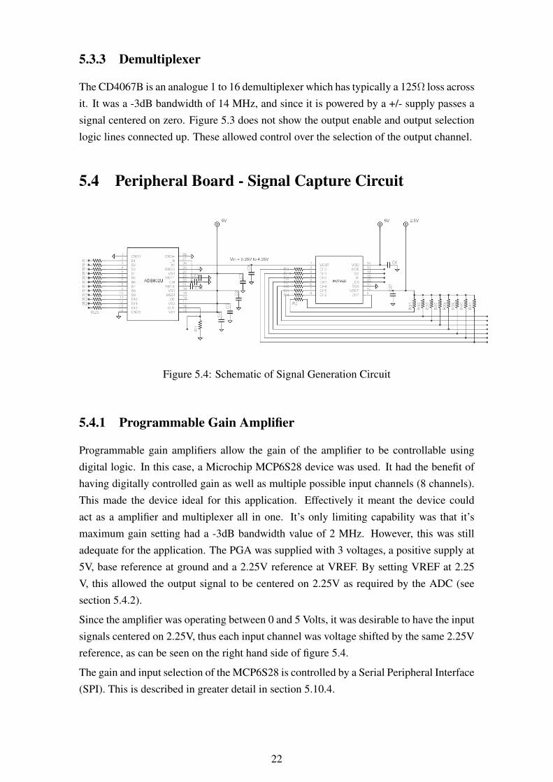
5.4 Peripheral Board - Signal Capture Circuit
Figure 5.4: Schematic of Signal Generation Circuit
5.4.1 Programmable Gain Amplifier
Programmable gain amplifiers allow the gain of the amplifier to be controllable usingdigital logic. In this case, a Microchip MCP6S28 device was used. It had the benefit ofhaving digitally controlled gain as well as multiple possible input channels (8 channels).This made the device ideal for this application. Effectively it meant the device couldact as a amplifier and multiplexer all in one. It’s only limiting capability was that it’smaximum gain setting had a -3dB bandwidth value of 2 MHz. However, this was stilladequate for the application. The PGA was supplied with 3 voltages, a positive supply at5V, base reference at ground and a 2.25V reference at VREF. By setting VREF at 2.25V, this allowed the output signal to be centered on 2.25V as required by the ADC (seesection 5.4.2).
Since the amplifier was operating between 0 and 5 Volts, it was desirable to have the inputsignals centered on 2.25V, thus each input channel was voltage shifted by the same 2.25Vreference, as can be seen on the right hand side of figure 5.4.
The gain and input selection of the MCP6S28 is controlled by a Serial Peripheral Interface(SPI). This is described in greater detail in section 5.10.4.
22
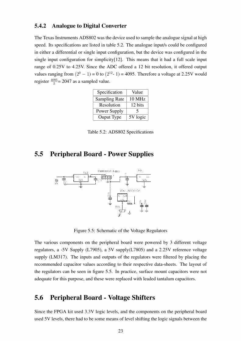
5.4.2 Analogue to Digital Converter
The Texas Instruments ADS802 was the device used to sample the analogue signal at highspeed. Its specifications are listed in table 5.2. The analogue input/s could be configuredin either a differential or single input configuration, but the device was configured in thesingle input configuration for simplicity[12]. This means that it had a full scale inputrange of 0.25V to 4.25V. Since the ADC offered a 12 bit resolution, it offered outputvalues ranging from (20 − 1) = 0 to (212- 1) = 4095. Therefore a voltage at 2.25V wouldregister 4095
2= 2047 as a sampled value.
Specification ValueSampling Rate 10 MHz
Resolution 12 bitsPower Supply 5Ouput Type 5V logic
Table 5.2: ADS802 Specifications
5.5 Peripheral Board - Power Supplies
Figure 5.5: Schematic of the Voltage Regulators
The various components on the peripheral board were powered by 3 different voltageregulators, a -5V Supply (L7905), a 5V supply(L7805) and a 2.25V reference voltagesupply (LM317). The inputs and outputs of the regulators were filtered by placing therecommended capacitor values according to their respective data-sheets. The layout ofthe regulators can be seen in figure 5.5. In practice, surface mount capacitors were notadequate for this purpose, and these were replaced with leaded tantalum capacitors.
5.6 Peripheral Board - Voltage Shifters
Since the FPGA kit used 3.3V logic levels, and the components on the peripheral boardused 5V levels, there had to be some means of level shifting the logic signals between the
23

peripheral board and the FPGA kit. This was accomplished by using M74HCT541 OctalNon-Inverting buffer devices where needed. The 5V voltages originating at the ADC weresimply current limited by placing 2K resistors on each logic line, thereby protecting theFPGA pins from high current load and bypassing the need for a return 5V-to-3.3V shifter.This configuration can be seen in the final schematic in the appendix A.
5.7 Peripheral Board - Board Fabrication
The schematics and assembly for the peripheral board where done in Eagle CAD. Theresulting PCB was printed using UCT’s recently purchased fast prototyping machine.The process involves placing a protective film over the blank copper-silicon-copper plate,drilling the through holes and vias, then applying solder paste to couple the vias. Oncethis was done, the film was removed and the plate was placed in an oven for 30 minutesto set the solder paste. The plate was then placed back into the prototyping machine forit’s tracks to be etched out of the copper, and the periphery of the board to be cut from therest of the plate, leaving the remaining plate reusable.
The components used on the board were all obtained using sample requests from the re-spective chip manufacturers. Passive surface mount components were bought in reelsfrom a local distributor. The process of soldering was tedious, but resulted in a very func-tional board, which suffered from relatively few problems. As stated in section 5.5, someleaded tantalum capacitors were used instead of the surface mount ones, as they provedto provide better decoupling for the power supplies. Initially there was a misconceptionabout part of the data-sheet for the programmable gain amplifier, and an additional powersupply was used unnecessarily. This was removed and the board was patched. The volt-age level shifting of the incoming signals from 0V to 2.25V as stated in section 5.4.1, wasactually done after the fabrication process by soldering the extra 2K resistors standing upvertically and then soldering a wire bridge across these resistors connecting them with the2.25V supply (see bottom right area of figure 5.6).
5.8 FPGA Kit and Peripheral Board Interface
There were a large number of logic channels that needed to be connected between theperipheral board and the FPGA kit. Figure 5.7 demonstrates how this was accomplishedusing normal parallel IDE cable. The pins on the peripheral board where laid out accord-ing to the channel they would match up with on the kit prototyping pins. These were theneasily connected using the cables and some pin headers on either side.
24

Figure 5.6: The assembled peripheral board
Figure 5.7: Nios II Evaluation Kit Interfaced with the custom made peripheral board
25

5.9 Nios II Evaluation Kit
The platform on which the processing capabilities of this system were built, and on whichfuture work will be done, was the Altera Nios II Evaluation Kit. The kit is meant to bean evaluation board for the Nios II soft-core processor, although it can be used for anypurpose for which it meets the requirements. It is composed of a FPGA device (the AlteraCyclone FPGA), and accompanying crystal oscillators, voltage regulators and standardinterfaces (JTAG, Serial, Ethernet and straight logic prototyping pins). The basic layoutis as shown in figure 5.8. This kit comes with all the tools necessary to develope pro-grammable images for the FPGA device, as well as an IDE to create software for the NiosII soft-core processor.
Figure 5.8: Basic Layout of Nios II Evaluation Kit, courtesy of [13]
5.10 Nios II Soft-core Processor & Peripherals
5.10.1 Overview
The Nios II is a 32-bit embedded software defined processor that is almost entirely config-urable, providing a best-fit configuration for any application. Since it is software defined,the Nios II can be modified by adding or removing various peripheral components, aswell as choosing which type of Nios II core to use based on desired core attributes:
Fast with Large Footprint
26

Standard with Medium Footprint
Economy with Small Footprint
The Fast has the fastest performance (measured in Dhrystone MIPS), and the largest logicfootprint, whilst the Economy has the slowest performance but with the smallest logicfootprint. The advantage of the software defined nature of the Nios II is that custom in-structions can be placed alongside existing instructions in the ALU of the processor. Thisallows designers to tweak the performance of the processor for their application. The pro-cessor also comes complete with a standardized Avalon Bus to allow it to communicatewith embedded peripherals and even additional software-defined processors[14]. Figure5.9 demonstrates how the processor and it’s peripheral embedded components where con-figured. For this project, the Nios II was implemented with a Fast core and with the extraperipherals shown in the figure.
Figure 5.9: Configuration of the Nios II processor and it’s peripherals
5.10.2 Configuration using SoPC Builder
SoPC Builder (System-on-programmable-Chips) allows the basic Nios II processor to becustomized by configuring it’s core size, cache sizes, custom instructions and also it’speripheral components and interfaces. The SoPC builder produces a single HDL blockwhich contains the core processor, the Avalon Bus (see figure 5.9) and all peripheralcores. This block is then imported into the Quartus CAD software to be interfaced withthe other custom on-board components, and to allow it to be connected to external FPGApins. Figure 5.10 shows the customized Nios II processor block built for this project usingSoPC builder and imported into the Quartus CAD environment. External pins are shown
27

with their names, which are allocated by a template provided with the Cyclone FPGAtool-set.
Figure 5.10: The Nios II HDL block configured with the corresponding pins
5.10.3 PIO Interface
In order for the processor to send and receive logic signals from the external peripheralboard (see sections 5.3, 5.4, 5.5 and 5.6), it needed an interface with which to bufferthe associated I/O logic. This facility is called the PIO core which is interfaced withthe processor through the Avalon Bus. It comes as a standard peripheral with the NiosII processor. The processor addresses the PIO core as a bus address, just like any othercore component attached to the processor. Thus it is possible to have multiple PIO coreswhich allowed for a PIO core for every device on the peripheral board that needed a logicalinterface. This had the added benefit of simplifying the control code (section 6.2) greatly,since each PIO core could be addressed using its own address or variable name, ratherthen performing bit masking for a single core. By examining figure 5.10, the differentPIO Cores and their output pins can be seen, running second segment from the top of theprocessor block downwards. These are further elaborated by table 5.3.
5.10.4 SPI Interface
The Programmable Gain Amplifier uses a SPI interface to accept commands that controlthe switching of it’s input channels, gain and power state. The Nios II comes with a SPIcore which can also be interfaced with the processor through the Avalon Bus in exactly
28

PIO Core FunctionADC_clk To interface with the ADC’s clock pinADC_in To interface with the ADC’s 12 output pinsDAC_clk To interface with the DAC’s clock pinDAC_out To interface with the DAC’s 14 input pins
DEMUX_inhibit To interface with the Demultiplexor’s inhibit pinDEMUX_select To interface with the Demultiplexor’s channel select pins
SV2 To interface with the extra pins on the board (wasn’t used)extra_pins Bidirectional Interface to extra pins on the peripheral board (wasn’t used)
Table 5.3: The different PIO cores and their functions
the same way as the PIO Core. This SPI core accepts values to be written to the SPI deviceand automatically controls the transfer according to the specifications of the SPI standard(timing, bit-rate etc). It can be set as a slave or master device and handle multiple otherdevices on the same interface, however in this case it was implemented as a master SPIdevice controlling a single slave device (the PGA). The SPI interface appears in figure5.10 as the segment 2ndfrom the bottom.
5.10.5 Cyclone Pin-out Interface
The bottom of the Cyclone 1C12 FPGA device is an array of pin connectors that is mappedout by figure 5.11. The pads on which the cyclone is soldered are hardwired to individualpins on the prototyping area of the Nios II Evaluation Kit (see right hand side of figure5.8). The yellow blocks in figure 5.11 indicate where prototyping pins have been mappedto. This means that the hardware image created by Quartus must have it’s appropriateI/O lines correctly matched with the positions in the figure. In order to do this, the pinallocation facility in Quartus was used. This allows the designer to specify a FPGA pinfor every pin that appears in the CAD design (see figure 5.10).
29

Figure 5.11: Cyclone 1C12 Functional Pin-out, courtesy of [13]
30

Chapter 6
Software Implementation
This chapter describes how the project software was designed and created using the soft-ware tools supplied with the Nios II Evaluation Kit. The Nios II IDE is a programmingenvironment shipped with Evaluation Kit. It automatically creates a hardware abstractionlayer (see section 6.1) for a custom Nios II configuration. Application code can then bewritten that uses functions exported by the HAL, and during the compiling process, thedrivers, HAL and application code are all linked and bundled together. The applicationcode for this project can be seen in appendix C. The chapter also describes how the rawdata was processed in Matlab to produce visual information, in order to determine if thesystem was working as planned, and to provide the results shown in chapter 7.
6.1 Hardware Abstraction Layer
The SoPC builder software described in section 5.10.2 automatically memory maps theadditional peripheral cores into the processor’s accessible memory space. This meansthat the processor “sees” these additional peripherals as normal memory addresses. Thisallows these memory address values to be assigned to variable names, so that procedurescan be written to abstract away the low-level interface with peripheral components.
In fact, SoPC builder has the ability to create a HAL (Hardware Abstraction Layer) for anindividual Nios II configuration and exports this as C code with associated library files.This means that all that needs to be done is to write the application code for system byusing calls to the exported functions provided by the HAL. This dramatically speeds upthe development time, and it is for this reason that the code here is so simple. The actuallow-level hardware interfacing code has been abstracted away.
Wherever possible , this HAL exports it’s functions as ANSI C Standard Library functionlook-alikes, such as fopen(), fwrite() and printf()[15]. This allows the programmer to ac-cess the peripherals using standard C function calls. Obviously this is not always possible,as certain devices do not fit the Standard C model for data streams, file access etc. Oneexample of such a device is the SPI Core. Figure 6.1, taken from [15], but modified forthe project scenario, demonstrates how the HAL fits in with the software model.
31

Figure 6.1: The HAL fitted into the project software model
6.2 Control Code
6.2.1 Overview
This section explains how the software which controls the ultrasound scanner works.Since the system was a prototype design and there was limited development time, thesystem was controlled by commands sent to the processor using the JTAG debug inter-face. The JTAG module was capable of performing the following functions [taken from[16]]:
• Downloading application software into the SDRAM
• Starting and stopping the program execution
• Setting breakpoints and watchpoints
• Analyzing registers and Memory
• Collecting real-time execution trace data
• Interfacing the program with a GDB server (see section 6.3)
Now , even though the JTAG module would potentially slow the processor down by plac-ing breakpoints in the code, it was possible to use only a stripped down version of theJTAG module which only allowed for a serial interface with the PC, and allowed forbreakpoints to be ignored. It was noted that this had no effect on the speed at whichthe processor ran, even though the JTAG serial interface is very slow. Only when a datastream was written or read from the JTAG interface was there a reduction in speed. Thisallowed the whole scanning process to be controlled via a JTAG serial interface. The ap-plication software was extremely basic and allowed a user to set the required gain, and toinstruct the system to perform a scan. The algorithm for program control is represented
32

Figure 6.2: Flow chart of main control software
33

by the flow chart in figure 6.2, whilst figure 6.3 shows the flow chart for performing ascan.
Figure 6.3: Flow chart of scanning algorithm
34

6.2.2 Synthesized Sine Wave Generation
In order to generate a basic 40 KHz sine wave to be transmitted as a test signal, it wasnecessary to have knowledge of the sampling speed capabilities of the processor. Whencertain hardware is programmed into the FPGA, the Quartus auto-routing software makesestimates of the latency of certain instructions, but these can only be confirmed by testingthe final design.
In order to determine at what speed the processor could spit out data values to the DAC, asimple test program was created. This application essentially had a loop that read a valuefrom memory, sent this value to the DAC, and then toggled the DAC clock. This loopran repeatedly and the voltage on the clock line was analyzed using an oscilloscope. Theclocking frequency was found to be 1.267 MHz.
Figure 6.2 indicates that a wave look-up table is created after system initialization andbefore control is passed to the user. The sampling frequency above was using to createthe sine table of sample values in memory that could be fed at a rate of 1.267 Mega-samples-per-second to the DAC. The pseudo code in figure Figure 6.4 on page 35 showshow the table was filled with 100 samples of a sine wave: Here the DAC_RES value
Figure 6.4: Pseudo code for generating a sine wave table
is the decimal resolution of the DAC, which in this case is a full scale range of 214=16384 different possible values. In other words, after reviewing section 5.3.1, a value of0 applied to the DAC will give an output voltage of -3.75V and a value of 16384 will givea full-scale voltage at +3.75V. Figure 6.5 demonstrates what the generated wave of 100samples would look like. Note how the last value is not zeroed, but this is not importantas the output voltage is returned to zero by stabilizing the voltages (see figure 6.3)
6.2.3 Wave Capture
The same test was done for reading in values from the ADC. A loop was run that firstclocked the ADC, read a value from the output lines of the ADC, then wrote the integervalue into memory. The oscilloscope showed that the result was exactly the same as whenreading from memory, 1.267 MHz. This effectively meant that the expected 40.5KHzultrasound wave, could be sampled at 1.267 MHz, or over 31 times its own Nyquist limit.
35

Figure 6.5: Generated sin wave values ready for transmission
This would give a very accurate representation of the resultant wave. The process ofsampling a resultant wave was simple. For sampling, simply begin clocking the ADC at1.267 MHz when the transmitted wave was finished being sent, (as show in figure 6.3)and in between clock cycles, read off the value on the output of the ADC. The capturedsample should have a brief time of no activity and then as the first sound pulse arrives atthe receiver, a sudden rise of values. We are interested only in the time of this first pulse,as explained in section 3.2. A sampling size of 1000 was decided upon, as a sufficientsize sampling to catch the incident wave in it’s entirety, even for the longest trajectory.The whole set of values captured by the scanning process depicted in figure 6.3 wouldtherefore be 8 transmitters * 8 receivers * 1000 samples = 64,000 samples. If each sampleoccupied 2 bytes in memory (16 bits) this would give a total memory requirement of 2 *64,000 / 1024 = 125 KBytes, an amount easily matched by the Evaluation Kit’s 16 MB ofSDRAM.
6.3 GDB Server
Section 4.4.2 called for a data repository were the wave capturing system could perma-nently store the raw sampled data retrieved using the scanning process. Since the systemwas being operated via a JTAG interface (an interface meant for debugging) is was con-venient to make use of a GDB server facility. GDB stands for GNU Debugger, and it
36

provides a means for the application running on the Nios II processor to be able to writea file on the remote PC just as if it was writing to it’s own local file-system. This processis still limited by the speed of the JTAG interface, but is much more efficient then sendingthe data back on the JTAG command shell interface as ASCII text. By executing the ap-plication through the Nios II IDE with a GDB server enabled, the target application couldwrite a binary file on the host machine. Thus as long as the SDRAM on the FPGA kit wasbig enough to hold one set of sampled values, the system had a fail-safe data repository.
In order to send the files back to the host PC, the standard C file handling procedures wereused. This included using file pointers, and the fwrite() command. The data was writtenby sequentially writing the 12 bit samples, packaged as 16 bit binary values, to the openedfile. This created a file size of 125 KBytes, as demonstrated at the end of section 6.2.3.Thefile was then opened in Matlab do perform some signal processing, which is explained inthe next section.
6.4 Data Processing in Matlab
6.4.1 Finding the TOF Value
Once the raw data was held as a binary file, it could be opened using Matlab and analyzed.The purpose of this processing was to extract the Time-of-flight (TOF) information fromthe raw data and graph this information so that the system’s validity could be verified.Figure 6.6 demonstrates the procedure followed to produce TOF information from theraw data. In order to prepare the data for processing, the binary values were read into a3-dimensional (8 * 8 * 1000) array. Now since the ADC produces 12 bit binary values thatrepresent a range of 0 to 4096, centered on 4096 / 2 = 2048, it was necessary to subtracta value of 2048 from each sample to produce values centered around zero. Then for eachof the 64 of the sets of 1000 samples a common procedure was applied, and for each seta time-of-flight value was produced and placed in a 3D (8*8*1) array. The following listdescribes the reasoning behind each step shown in the flowchart (figure 6.6).
1. Fast Fourier Transform - To find the signal’s frequency spectrum, the Matlab fft()
function was used. This produced a set of 1000 complex numbers, and for each ofthese the absolute value was taken.
2. Zero-ing the DC frequency value and values after the 500th sample - Becauseof the inaccuracy of the 2.25V reference on the peripheral board, the signals weren’tcentered exactly on zero, therefore the DC component needed to be removed. In thediscrete frequency domain, the DC component is found in the sample representingzero Hertz. This value was forced to be zero. In order to find the TOF value, onlythe envelope of the signal waveform was needed so that the first pulse edge can
37

Figure 6.6: Overview of procedure used to extract TOF values
be found. The envelope was found by zero-ing all the negative frequency compo-nents (those values represented in sample 501 up to and including 1000) and thenapplying the ifft() in step 3.
3. Inverse Fourier Transform - The ifft() Matlab function was used to convert thediscrete frequency domain values back into the time domain. By doing so, just theenvelope of the original signal is found. Although the first rising edge could still bedetected using the the original signal, the “cleaned up” envelope signal provides abetter waveform from which to find the the TOF value.
4. Signal Smoothing - In order to further clean the waveform, the signal is smoothedusing a 10-point moving average weighting (the Matlab smooth() function)
5. Calculation of threshold value - A suitable means of finding the first rising edge
38

(indicating the arrival of a ultrasound pulse) was found using trial and error. Mostalgorithms find the rising edge by looking for the index of the point where the signalfirst crosses a “universal” threshold value that is preset. In this case, however, auniversal value was ineffective as different signal paths produced wildly differentamplitudes and it was possible for the threshold to be missed completely or perhapstriggered by noise. Instead, the maximum value in the set of 1000 values wasfound. This value was halved, and the halved value became the threshold for thatset of samples.
6. Finding Threshold Crossing - Once the threshold value was determined, the setof 1000 samples was searched for the index of the first value to pass the thresh-old value. It was necessary to ignore the first 50 samples, as sometimes spuriousmedium amplitude signals could be found (probably due to circuit feedback).Thisproved to be quite an effective way of discovering the first rising edge and thereforethe TOF value.
7. Recording Index as TOF - Once the TOF value was found, it was recorded in itsappropriate index in the 8 * 8 array of TOF values.
6.4.2 TOF Example Set
This subsection serves to illustrate the process outlined in the previous section by visual-izing the process through its various stages. It follows the process of analyzing one set of1000 samples to find its TOF value.
• Firstly a raw set of 1000 samples was extracted from the binary file, figure 6.7shows the extracted signal.
• Next the Fast Fourier Transform is applied to the sample set; see figure 6.8
• Next the DC component is zero-ed and the negative frequencies are also zero-ed.;see figure 6.9
• Next the sample set is Inverse-Fourier Transformed back into the time domain; seefigure 6.10
• Next sample set is smoothed to remove unwanted spurious edges; see figure 6.11
• Next the maximum value is found, this value is halved and the first intersection ofthe result is located. This becomes the TOF value; see figure 6.12
39

Figure 6.7: Original Sample Signal
Figure 6.8: Sample set in the frequency domain
Figure 6.9: Sample set in frequency domain with zero-ed DC and negative frequencies
40

Figure 6.10: Sample set envelope
Figure 6.11: Sample set envelope with smoothing applied
41

Figure 6.12: Sample set with threshold and TOF determined
42
Chapter 7
Test Results
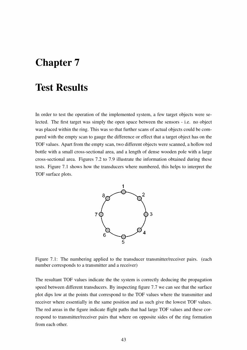
In order to test the operation of the implemented system, a few target objects were se-lected. The first target was simply the open space between the sensors - i.e. no objectwas placed within the ring. This was so that further scans of actual objects could be com-pared with the empty scan to gauge the difference or effect that a target object has on theTOF values. Apart from the empty scan, two different objects were scanned, a hollow redbottle with a small cross-sectional area, and a length of dense wooden pole with a largecross-sectional area. Figures 7.2 to 7.9 illustrate the information obtained during thesetests. Figure 7.1 shows how the transducers where numbered, this helps to interpret theTOF surface plots.
Figure 7.1: The numbering applied to the transducer transmitter/receiver pairs. (eachnumber corresponds to a transmitter and a receiver)
The resultant TOF values indicate the the system is correctly deducing the propagationspeed between different transducers. By inspecting figure 7.7 we can see that the surfaceplot dips low at the points that correspond to the TOF values where the transmitter andreceiver where essentially in the same position and as such give the lowest TOF values.The red areas in the figure indicate flight paths that had large TOF values and these cor-respond to transmitter/receiver pairs that where on opposite sides of the ring formationfrom each other.
43

Figure 7.2: Photograph of Red Bottle under test scenario
Figure 7.3: Photograph of Wooden Pole under test scenario
Most importantly, by comparing figures 7.7 and 7.8 we can see that the red bottle hashad a noticeable influence on the TOF values, indicated by the rising TOF values corre-sponding to flight paths that intersect the centre of the ring formation. These are pathsthat intersected the red bottle neck and would thus be effected by its presence.
Figures 7.6 and 7.9 show how when the wooden pole was scanned, it seemed the ultra-sound waves did not penetrate the wood at all. This was probably due to the transmittedsignals lack of power (a peak-to-peak amplitude of 7.5 V) or perhaps the fact the factthat the transducers where not directly coupled with the wood. The result of this was thatthe TOF readings for the paths that intersected the wood, were simply close to 0. Thiswas because the receiver only picked up random noise and thus this upset the rising-edgefinding process.
From all the results shown, it is obvious that the system is however, not fine tuned. For
44

Figure 7.4: Test Subject: Empty space - raw sampled signals
example, the raw data samples in figure 7.4 are not centered precisely on zero, and theyfall well within the range of -500 to 500 in value. Compare this to the resolution of thesystem (12 bits) and we can see the values should vary between -2048 and 2048. Thisindicates that the full receiver gain of 32 was inadequate, even when no target object wasthere to cause signal loss. It also indicates that a more powerful ultrasound signal shouldbe generated at the transmitters, to properly penetrate the target object.
45

Figure 7.5: Test Subject: Red Bottle - raw sampled signals
Figure 7.6: Test Subject: Wooden Pole - raw sampled signals
46

Figure 7.7: Test Subject: Empty space - surface plot of TOF values
Figure 7.8: Test Subject: Red Bottle - surface plot of TOF values
47

Figure 7.9: Test Subject: Wooden Pole - surface plot of TOF values
48

Chapter 8
Conclusions
After considering the results acquired from testing the system, it is evident that the overalldata acquisition unit works precisely as planned according to the specifications in chapter4. The high resolution 12 bit signal sampling as well as the relatively high speed at whichthe peripheral board operates, demonstrate that the system is capable of extracting highquality information from the testing environment.
It is clear that the digital side of the system works extremely well, and has vast room forincreased speed and exploitation of its resolution. The processing in Matlab producedvalid results that correlated well to expected readings. However the results obtained alsodemonstrated that the signals arriving at the ADC are not calibrated to exploit the full-scale input range of the device. The reasons for this include a weak transmission signalwith a maximum peak-to-peak output of 7.5V at the transmitters. This signal is attenuatedto such an extent through dense material such as wood that only noise is read at thereceiver end. Another reason is lack of gain at the receiver end. The design choice ofusing the PGA to reduce circuit size meant a weak maximum gain of 32 which provedinadequate for preparing received analogue signals to be fed into the ADC.
Another point of note is the speed at which the whole scanning process occurs . Theentire 64 sets of 1000 samples took less then 1 second to collect each time a target wasscanned. However the process of getting this data back to the PC to be processed is slowand very manual, as are the Matlab DSP procedures. The end visualization depends onlyon the TOF values. Thus it can easily be seen how the only data that should be sent backfrom the FPGA to the PC or laptop, should be the TOF values, meaning the digital signalprocessing should take place entirely on-board the FPGA. This could potentially providethe capabilities for a real-time ultrasound tomography device. This was however foreseen,and the final conclusion is that the implemented system provides an excellent frameworkfor future work into a soft-core DSP block.
49

Chapter 9
Recommendations and Proposals
Considering the conclusions discussed in chapter 8, the following extensions to this topicare proposed:
• An overhaul of the analogue side of the system implemented in this project. Thegoals of which would be to:
– generate much more powerful ultrasound waves at the source transducers
– provide more gain at the receiving end.
– provide for more transducers in the array (at least 16), giving more propaga-tion paths and greater resolution.
– redesign the transducer housing for greater stability and directional accuracy
• To design and implement a soft-core digital signal component that can be pro-grammed into the FPGA alongside the Nios II processor to facilitate real-timedigital signal processing. This should specifically include (see figure 9.1 for anillustration):
– a signal generation core that should generate a predefined digital signal andfeed this out to the DAC at a constant specified sample rate.
– a DSP core that would interface directly to the external ADC and would readin samples and clock the ADC at a constant specified sampling rate. The unitshould process the received signal in real-time, and extract the TOF valueswhich could then be passed to the Nios II processor.
– the compatibility of the above two components with the Nios II Avalon Bus.
• To integrate ethernet capabilities into the system. This would allow the FPGA de-vice and peripheral board to operate in a location that is remote from the placewhere the extracted data is visualized. This could be done quite easily with theNios II , a proper FPGA Development kit (instead of the Evaluation Kit) and ap-propriate licenses.
50

Figure 9.1: Proposed signal generation and DSP core configuration
51

Appendix A
Peripheral Board Schematic
52

53

Appendix B
Peripheral Board Assembly
54

55

Appendix C
Software Source Code
The following is the C code that was writen in the Nios II IDE and executed on the NiosII processor. Note the library generated HAL and assoicaited libraries are not included.
/*************************** control.c ****************************/
#include <stdio.h>
#include <math.h>
#include <string.h>
#include <unistd.h>
#include "system.h"
#include "sys/alt_irq.h"
#include "altera_avalon_pio_regs.h"
#include "altera_avalon_spi.h"
#include "sys/alt_timestamp.h"
#include "alt_types.h"
#define PI 3.141592653 //Value of Pi
#define DAC_SAMPLES 100 //Number of DAC Samples to generate
#define ADC_SAMPLES 1000 //Number of ADC Samples to capture
#define DAC_RESOLUTION 16384 //2^14 bits is 16384 in decimal
#define FREQ 40500 //The desired frequency of the generated ultrasound wave
#define MAX_FREQ 1266666 //This is the maximum output switching
//freq the hardware is capable of.
#define NUM_INPUT_CHANNELS 8
#define NUM_OUTPUT_CHANNELS 8
static alt_u16 ADC_Data[NUM_INPUT_CHANNELS][NUM_OUTPUT_CHANNELS][ADC_SAMPLES];
static alt_u16 DAC_Data[DAC_SAMPLES];
static void clock_ADC() //clocks the ADC by one cycle.
IOWR_ALTERA_AVALON_PIO_DATA(ADC_CLK_BASE,0xf);
IOWR_ALTERA_AVALON_PIO_DATA(ADC_CLK_BASE,0x0);
static void clock_DAC() //clocks the DAC by one cycle.
IOWR_ALTERA_AVALON_PIO_DATA(DAC_CLK_BASE,0xf);
IOWR_ALTERA_AVALON_PIO_DATA(DAC_CLK_BASE,0x0);
static void set_gain(int gain)
alt_u8 wdata[2];
alt_u8 rdata[4];
wdata[0] = 0x40;
switch (gain)
case 1:
wdata[1] = 0x00;
56

break;
case 2:
wdata[1] = 0x01;
break;
case 4:
wdata[1] = 0x02;
break;
case 5:
wdata[1] = 0x03;
break;
case 8:
wdata[1] = 0x04;
break;
case 10:
wdata[1] = 0x05;
break;
case 16:
wdata[1] = 0x06;
break;
case 32:
wdata[1] = 0x07;
break;
default:
wdata[0] = 0x00;
alt_avalon_spi_command(SPI_BASE,0,2,wdata,0,rdata,0);
static void set_input_channel(unsigned int chan)
alt_u8 wdata[2];
alt_u8 rdata[4];
wdata[0] = 0x41;
switch (chan)
case 0:
wdata[1] = 0x00;
break;
case 1:
wdata[1] = 0x01;
break;
case 2:
wdata[1] = 0x02;
break;
case 3:
wdata[1] = 0x03;
break;
case 4:
wdata[1] = 0x04;
break;
case 5:
wdata[1] = 0x05;
break;
case 6:
wdata[1] = 0x06;
break;
case 7:
wdata[1] = 0x07;
break;
default:
wdata[0] = 0x00;
alt_avalon_spi_command(SPI_BASE,0,2,wdata,0,rdata,0);
57

static void set_output_channel(unsigned int chan)
alt_u8 temp = chan & 0xf;
IOWR_ALTERA_AVALON_PIO_DATA(DEMUX_SELECT_BASE,temp);
static void generate_sine_wave(int freq) //fills the DAC array with a sine wave
int count;
double temp;
double samples_per_oscillation = ((double)MAX_FREQ / (double)freq);
double delta_t = (1 / (double)(MAX_FREQ));
unsigned int multiplier = DAC_RESOLUTION / 2;
printf("Sine Wave: samples_per_oscillation = %f \n",samples_per_oscillation);
printf("Sine Wave: delta_t = %f seconds \n",delta_t);
printf("Sine Wave: multiplier = %u seconds \n",multiplier);
printf("Sine Wave: Generating %f seconds of sound\n",(delta_t * DAC_SAMPLES));
for (count = 0; count < DAC_SAMPLES; count++)
temp = sin(2*PI*freq*delta_t*count);
temp = temp * multiplier;
temp = temp + multiplier;
DAC_Data[count] = (unsigned int)floor(temp);
printf("Sample of generated data:\n");
for (count = 0; count < 20;count ++)
printf("data[%d] = %u\n",count,(unsigned int)DAC_Data[count]);
static void stabilize()
IOWR_ALTERA_AVALON_PIO_DATA(DAC_OUT_BASE,0x2000);
clock_DAC();
clock_ADC();
clock_ADC();
clock_ADC();
clock_ADC();
clock_ADC();
clock_ADC();
static void perform_scan()
register unsigned int count;
unsigned int outer,inner;
//Steady both DAC and ADCs for transmission
stabilize();
usleep(1000);
for (outer = 0; outer < NUM_OUTPUT_CHANNELS; outer++)
set_output_channel(outer);
for (inner = 0; inner < NUM_INPUT_CHANNELS; inner++)
set_input_channel(inner);
usleep(10000); //wait for voltages to settle
for (count = 0; count < DAC_SAMPLES; count++)
IOWR_ALTERA_AVALON_PIO_DATA(DAC_OUT_BASE,DAC_Data[count]);
clock_DAC();
58

for (count = 0; count < ADC_SAMPLES; count++)
clock_ADC();
ADC_Data[inner][outer][count] = IORD_ALTERA_AVALON_PIO_DATA(ADC_IN_BASE);
printf("Acquired: OutChan[%d],InChan[%d]\n",outer,inner);
stabilize();
usleep(1000);
void print_results_binary()
unsigned int outer,inner;
FILE* fp = NULL;
printf("Attempting to Open data_bin .....\n");
fp = fopen ("/mnt/host/data.bin", "w");
if (fp == NULL)
printf ("Cannot open file data.bin\n");
else
printf("Writing array values....\n");
for (outer = 0; outer < NUM_INPUT_CHANNELS;outer++)
for (inner = 0; inner < NUM_OUTPUT_CHANNELS; inner++)
fwrite(ADC_Data[outer][inner],2,ADC_SAMPLES,fp);
printf("Closing file.....\n");
fclose (fp);
printf("File Closed and Saved. \n");
int main(void)
FILE* fp;
char str[20] = "";
int count;
//Steady both DAC and ADCs for transmission
clock_ADC();
IOWR_ALTERA_AVALON_PIO_DATA(DAC_OUT_BASE,0x2000);
clock_DAC();
printf("Generating Sine table....\n");
generate_sine_wave(FREQ);
printf(".....Done\n");
/* Perform any necessary initialization commands */
clock_DAC();
clock_ADC();
fp = fopen ("/dev/jtag_uart", "r+"); //Open jtag-out for reading and writing
while (1)
printf("Please enter a command:\n");
fgets(str,10,fp);
59

if (!strcmp("g2\n",str))
printf("Changed Gain to: 2\n");
set_gain(2);
else if (!strcmp("g1\n",str))
printf("Changed Gain to: 1\n");
set_gain(1);
else if (!strcmp("g4\n",str))
printf("Changed Gain to: 4\n");
set_gain(4);
else if (!strcmp("g5\n",str))
printf("Changed Gain to: 5\n");
set_gain(5);
else if (!strcmp("g8\n",str))
printf("Changed Gain to: 8\n");
set_gain(8);
else if (!strcmp("g10\n",str))
printf("Changed Gain to: 10\n");
set_gain(10);
else if (!strcmp("g16\n",str))
printf("Changed Gain to: 16\n");
set_gain(16);
else if (!strcmp("g32\n",str))
printf("Changed Gain to: 32\n");
set_gain(32);
else if (!strcmp("scan\n",str))
printf("Peforming Scan.......\n");
perform_scan();
printf("........Done\n");
else if (!strcmp("print\n",str))
print_results_binary();
return(0);
60

Appendix D
Matlab Functions
D.1 readBin.m
function [data] = readBin(filename)
ADC_samples = 1000;
out_channels = 8;
in_channels = 8;
fid = fopen(filename,’rb’);
A = fread(fid, inf, ’uint16’);
fclose(fid);
figure
for I = 1:1:in_channels
for J = 1:1:out_channels
for count = 1:1:ADC_samples
data(I,J,count) = A((I*8-8+J)*1000-1000 + count) - 2048;
temp(count) = A((I*8-8+J)*1000-1000 + count) - 2048;
end
subplot(8,8,I*8-8+J);
plot(temp)
end
end
D.2 extractSampling.m
function [data] = extractSampling(array,in_chan,out_chan)
ADC_samples = 1000;
for I = 1:1:ADC_samples
data(I) = array(in_chan,out_chan,I);
end
61

D.3 findTOF.m
function [TOF] = findTOF(data)
ADC_samples = 1000;
in_channels = 8;
out_channels = 8;
figure
for i=1:1:in_channels
for j = 1:1:out_channels
temp = extractSampling(data,i,j);
spec = fft(temp);
spec(1) = 0;
for count=(ADC_samples/2 + 1):1:ADC_samples
spec(count) = 0;
end
temp = abs(ifft(spec));
temp = smooth(temp);
subplot(8,8,i*8-8+j);
plot(temp)
x = ADC_samples;
threshold = max(temp) / 2;
for count = 50:1:ADC_samples
if (temp(count) > threshold)
x = count;
break;
end
end
TOF(i,j) = x;
end
end
62
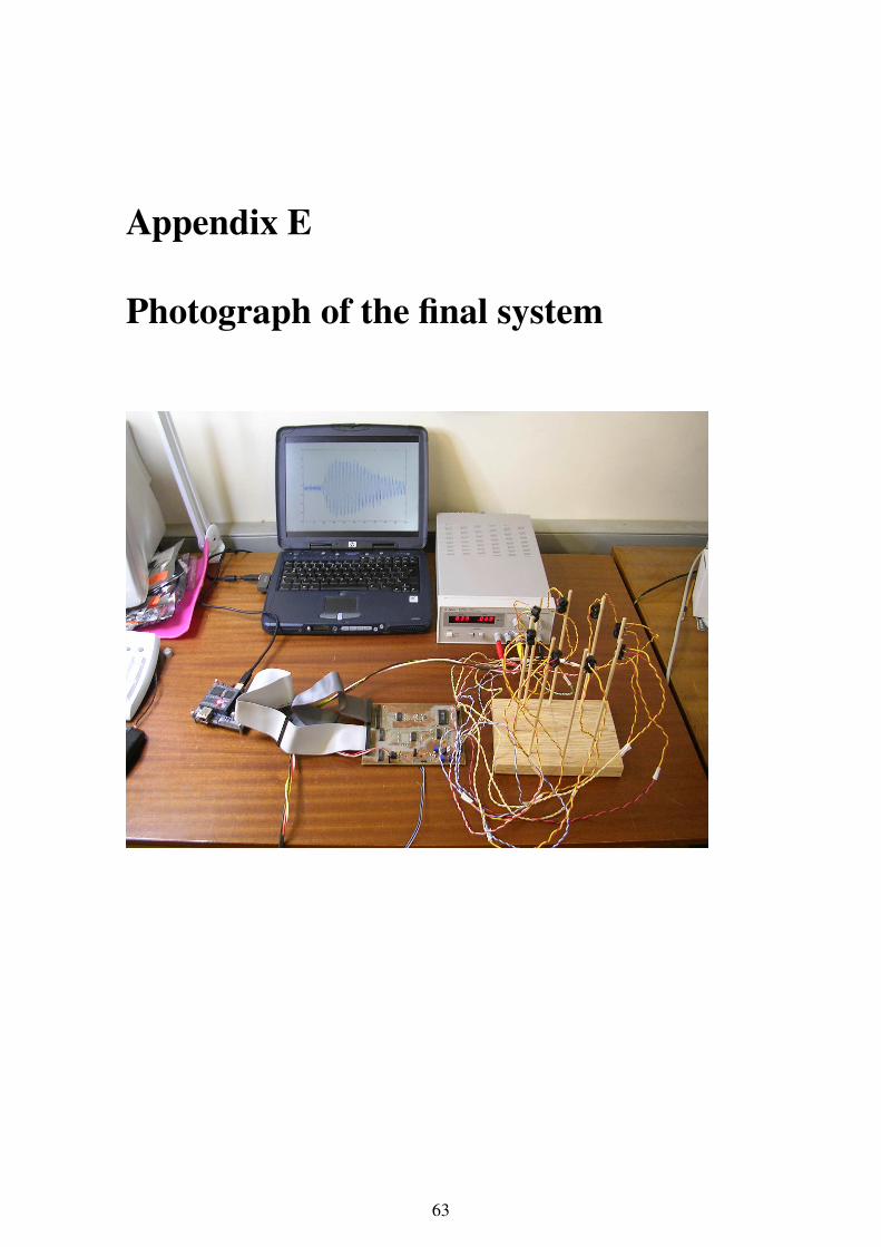
Appendix E
Photograph of the final system
63

Bibliography
[1] Field Progammible Gate Array, Wikipedia, http://en.wikipedia.org/wiki/FPGA, Oc-tober 2006
[2] Dicussions with Dr AJ Wilkinson (thesis supervisor)- Department of Electrical En-gineering, University of Cape Town, 2006
[3] David Pellerin, Scott Thibault, Practical FPGA Programming in C, Chapter 1, Pren-tice Hall 2005
[4] M. Morris Mano, Charles R. Kime, Logic and Computer Design Fundamentals 2nd
Edition Updated, Chapter 6, Prentice Hall 2001
[5] System-on-a-Chip, Wikipedia, http://en.wikipedia.org/wiki/System-on-a-chip, Oc-tober 2006
[6] Digital Set-Top Boxes & Integrated Digital Television Systems, Altera Corporation,
http://www.altera.com/end-markets/consumer/dtv/csm-digitaltv.html, October 2006
[7] Ultrasound Tomography, Zunaid Parker, University of Cape Town, October 2005
[8] Ultrsound, Wikipedia, http://en.wikipedia.org/wiki/Ultrasound, October 2006
[9] Sound, Wikipedia, http://en.wikipedia.org/wiki/Sound, Octover 2006
[10] Datasheet - DAC904, http://www.ti.com, August 2006
[11] Datasheet - MCP6S28, http://www.microchip.com, August 2006
[12] Datasheet - ADS802, http://www.ti.com, August 2006
[13] Nios II Evaluation Kit - Bundled Documentation, http://www.altera.com, August2006
[14] Nios II, Wikipedia, http://en.wikipedia.org/wiki/Nios_II, September 2006
[15] Nios II Software Developer’s Handbook, http://www.altera.com, August 2006
[16] Nios II Processor Reference Handbook, http://www.altera.com, August 2006
64