FPGA Architecture, Technologies, and Tools - ERNETneeraj/doc/fpga.pdf · FPGA Architecture,...
63
FPGA Architecture, Technologies, and Tools Neeraj Goel IIT Delhi
Transcript of FPGA Architecture, Technologies, and Tools - ERNETneeraj/doc/fpga.pdf · FPGA Architecture,...

FPGA Architecture, Technologies, and Tools
Neeraj GoelIIT Delhi

Jan 10, 2009 Neeraj Goel/IIT Delhi
PlanFPGA architecture
Basics of FPGA
FPGA technologiesArchitectures of different commercial FPGAs
FPGA toolsFPGA implementation flow and software involved
HDL coding for FPGASome coding examples and techniques

Jan 10, 2009 Neeraj Goel/IIT Delhi
What is FPGAFPGA – Field Programmable Gate Array
A programmable hardwareRelation between VHDL and FPGA
VHDL models hardware and FPGA implements the hardware modeled by VHDL
Relation between ASIC and FPGASame in functionalityFPGA are reprogrammable

Jan 10, 2009 Neeraj Goel/IIT Delhi
FPGA“Field Programmable Gate Array”A plane and regular structure in which logic and interconnect both are programmableProgrammability of logic – any combinational or sequential logic can be implementedProgrammability of interconnect – any logic component can be connected to anyone else

Jan 10, 2009 Neeraj Goel/IIT Delhi
ASIC verses FPGAFPGA
Low cost solutionLarger area, power and speedLess design and testing time
ASICLow cost for large volumeArea and power efficientHigh frequencies can be achievedHuge testing cost in term of time and money
Performance
Prog
ram
mab
ility
Proc
ASIC
FPGA

Jan 10, 2009 Neeraj Goel/IIT Delhi
Applications of FPGAsConventional applications
For design prototypingFor emulation
New applicationsAs hardware acceralatorIn place of ASIC– Less time to market
Complete System on Chip (SoC) solution

Jan 10, 2009 Neeraj Goel/IIT Delhi
Programming technologyAnti-fuse based
All the contacts or open initiallyProgramming converts selected locations as conductingOne time programmable (OTP)
SRAM basedE2ROM or Flash basedTradeoffs
Anti-fuse is less area, less power consumingE2RAM takes more time for programmingSRAM is technology leaders

Jan 10, 2009 Neeraj Goel/IIT Delhi
Programmable LogicFine grain “fabric”
A universal gate like NAND or AND-OR-NOTMiddle grain
Multiplexer basedROM/RAM based
Coarse grainFFT or a processor as a basic unit
TradeoffsFine grain FPGA involves more interconnection overhead Coarse grain are application specific

Jan 10, 2009 Neeraj Goel/IIT Delhi
Programmable LogicOp = X xor Y xor Z
OP
01101001
OP
XX’
X’X
Y
Y
Z
01 XYZ
MUX based
LUT based

A simple programmable logic block
Jan 10, 2009 Neeraj Goel/IIT Delhi
LUT
FF
abc
d
clock
y
q

Jan 10, 2009 Neeraj Goel/IIT Delhi
Programmable interconnectsConnection box
Connects input/output of logic block to interconnect channels
Switch boxConnects horizontal channels to vertical channels
Transmission gate (or a pass transistor) is used for each connection

Interconnections
Jan 10, 2009 Neeraj Goel/IIT Delhi
1
2
3
4
1
2
3
4
4 3 2 1
1234
Routing succeeded with a channel width factor of 3.
[9]
[1]
[21]
[10]
0
1
2
3
4
5
0
1
2
3
4
5
0
1
2
3
4
5
0
1
2
3
4
5
A switch box
A snapshot from VPR

Jan 10, 2009 Neeraj Goel/IIT Delhi
Top view of a simple FPGA Architecture
Routing succeeded with a channel width factor of 3.
pr
pt
ps
pq
ph
pg
pm
pn
pc
pd
pb
pa
pf
pe
out:pv
pu
pk
pl
po
pp
pj
pi
[110]
[111]
pv
[108]
[20]
[9]
[1]
[11]
[112]
[21]
[10]
[109]
[113]
[106]
[107]
A snapshot from VPR

Jan 10, 2009 Neeraj Goel/IIT Delhi
Review and questionsIs FPGA an ASIC?Can we implement an processor in FPGA?Are PLAs same as FPGA?The companies which produce FPGA?Why FPGAs are important to our VLSI?Do we need to study FPGA internals?

Questions?

Jan 10, 2009 Neeraj Goel/IIT Delhi
PlanFPGA architecture
Basics of FPGA
FPGA technologiesArchitectures of different commercial FPGAs
FPGA toolsFPGA implementation flow and software involved
HDL coding for FPGASome coding examples and techniques

Jan 10, 2009 Neeraj Goel/IIT Delhi
Advanced FPGA ArchitecturesCompanies
XilinxAlteraActelAmtelQuicklogic

Jan 10, 2009 Neeraj Goel/IIT Delhi
Xilinx FPGA ArchitectureBasic blocks are a logical cell
A 4 input LUT can also act as 16x1 RAM or Shift register
LUT
FF
abc
e
clock
y
qd

Jan 10, 2009 Neeraj Goel/IIT Delhi
Xilinx FPGA ArchitectureBasic blocks are a logical cellA slice comprise of two logic cellsA configurable logic block (CLB) may have upto 4 slices
CLB of XC4000 series have 1 sliceCLB of virtex series have 2 or 4 slices
A hierarchical structure help in reducing interconnections
Interconnections are costly resource in FPGA

Jan 10, 2009 Neeraj Goel/IIT Delhi
Xilinx FPGA Architecture: a CLB in XC4000
Source: xilinx.com

Jan 10, 2009 Neeraj Goel/IIT Delhi
Xilinx FPGA Architecture: a CLB in XC4000Two 4-input and one 3-input function generatorTwo latched outputs and two unlatched output
Fun.Gen.
Fun.Gen.
Fun.Gen.

Jan 10, 2009 Neeraj Goel/IIT Delhi
Xilinx FPGA Architecture: a CLB in XC4000One 9-input function generatorLatched or unlatched output
Fun.Gen.
Fun.Gen.
Fun.Gen.

Jan 10, 2009 Neeraj Goel/IIT Delhi
Xilinx FPGA Architecture: a CLB in XC4000One 9-input function generatorLatched or unlatched output
Fun.Gen.
Fun.Gen.
Fun.Gen.

Jan 10, 2009 Neeraj Goel/IIT Delhi
Xilinx FPGA Architecture: a CLB in XC4000function generator as RAM
Level triggered, edge triggered, single port, dual port16x2, 32x1, 16x1 bit array
Fun.Gen.
Fun.Gen.
D0
D1
G1..G4
H1..H4
16x2 single port bit array

Jan 10, 2009 Neeraj Goel/IIT Delhi
Xilinx FPGA Architecture: a CLB in XC4000function generator as 16x2 edge triggered single port RAM
Source: xilinx.com

Jan 10, 2009 Neeraj Goel/IIT Delhi
Xilinx FPGA Architecture: a CLB in XC4000Fast carry chains
Dedicated logic in F and G function generators for fast carry generationDedicated routing resources for carry chains

Jan 10, 2009 Neeraj Goel/IIT Delhi
Xilinx FPGA Architecture: InterconnectionsFive type of interconnection based on length
Single length lines, double length lines, Quad, Octal and long lines
Source: xilinx.com

Jan 10, 2009 Neeraj Goel/IIT Delhi
Xilinx FPGA Architecture: InterconnectionsSingle and double lines with programmable switch box
Source: xilinx.com

Jan 10, 2009 Neeraj Goel/IIT Delhi
Xilinx FPGA Architecture: Virtex arrayArchitecture overview
Source: xilinx.com

Jan 10, 2009 Neeraj Goel/IIT Delhi
Xilinx FPGA Architecture: Virtex arrayOne CLB – 2 slice
Source: xilinx.com

Jan 10, 2009 Neeraj Goel/IIT Delhi
Xilinx FPGA Architecture: Platform ComputingLatest FPGA features
4 slices in a CLBBlock RAMEmbedded multiplier and DSP blockEmbedded processors
– PowerPC, a hard core– Microblaze a soft core
Other interface cores Gbps rocket IOPartial reconfigurability

Jan 10, 2009 Neeraj Goel/IIT Delhi
Altera FPGA familiesSimilar to Xilinx FPGAs
Basic block is LE (logic element)Basic unit is LAB (Logic array block) equivalent to CLB
Platform computingMegaRAM®
DSP block having embedded multiplierNios® embedded processor

Jan 10, 2009 Neeraj Goel/IIT Delhi
Review and questionsEffect of new technologies
Good for DSP computing– Embedded multipliers and BRAMs
A new player in embedded computingA good solution for network applications
Are FPGA internals helpful for a designer?

Jan 10, 2009 Neeraj Goel/IIT Delhi
Questions?

Jan 10, 2009 Neeraj Goel/IIT Delhi
PlanFPGA architecture
Basics of FPGA
FPGA technologiesArchitectures of different commercial FPGAs
FPGA toolsFPGA implementation flow and software involved
HDL coding for FPGASome coding examples and techniques

Jan 10, 2009 Neeraj Goel/IIT Delhi
FPGA implementation flow
Logic Synthesis
RTL
Netlist Mapping
Place and Route
ConfigurationFPGA
Constraint file

Jan 10, 2009 Neeraj Goel/IIT Delhi
HDL SynthesisInput: HDL – VHDL or VerilogOutput: NetlistProcess
Analysis of the HDLBehavior synthesis steps include scheduling and binding
– Datapath and FSM are implemented
Logic synthesis is logic minimizationOutput is in terms of basic gates and flip-flopsAlso estimates area and delay

Jan 10, 2009 Neeraj Goel/IIT Delhi
HDL SyhthesisEDA Tools
SynplifyXilinx – XSTMentor – FPGA expressSynopsys – DC compiler

Jan 10, 2009 Neeraj Goel/IIT Delhi
MappingInput: Netlist and ucfOutput: FPGA specific logic and gatesProcess (
For LUT based FPGA– For k input LUT, find the sub-graph with k input and
one output
Tools: Vendor specific

Jan 10, 2009 Neeraj Goel/IIT Delhi
Place and RoutePlace
Place the LUTs physically close which are connected most
– Reduce the overall net length
RouteUse of routing resources to minimize the delay
– Router have the delay model of interconnects
Both place and route are NP complete problemHeuristics are usedMostly the process of placement and routing is iterative in nature
Configuration file generationBased on place and route data configuration file is generated

Jan 10, 2009 Neeraj Goel/IIT Delhi
FPGA configuration
Configurationbitstream

Xilinx tools flow
Jan 10, 2009 Neeraj Goel/IIT Delhi
Source: dev manual, Xilinx.com

Jan 10, 2009 Neeraj Goel/IIT Delhi
Design entry and synthesis
Source: dev manual, Xilinx.com

Jan 10, 2009 Neeraj Goel/IIT Delhi
Design implementation process
Source: dev manual, Xilinx.com

Jan 10, 2009 Neeraj Goel/IIT Delhi
Design entry and synthesisInput
Schematic– Basic cells– Core generator
HDLSynthesis process
Can have various different module– Each module is synthesized as different native
generic object (ngo) file– All ngo files are combined to form native generic
database (ngd) fileConstraints can be given as input to ngdbuildprocess

Jan 10, 2009 Neeraj Goel/IIT Delhi
Floorplanner
Supports hand-placement of FPGA componentsCreates FNF or UCF fileSome components like DLLs need to be placed manually

Jan 10, 2009 Neeraj Goel/IIT Delhi
FPGA Editor
Very powerful surgical toolCan change any configuration detail of FPGA
Placement of componentsConfiguration of CLB SlicesRouting of particular netsLogic inside the LUTs

Jan 10, 2009 Neeraj Goel/IIT Delhi

Jan 10, 2009 Neeraj Goel/IIT Delhi

Jan 10, 2009 Neeraj Goel/IIT Delhi
Timing Analyzer
Performs static analysis of the circuit performanceReports critical paths with all sources of delaysDetermines maximum clock frequency

Jan 10, 2009 Neeraj Goel/IIT Delhi
Xilinx tool flow revisited
Source: dev manual, Xilinx.com

Jan 10, 2009 Neeraj Goel/IIT Delhi
Questions?

Jan 10, 2009 Neeraj Goel/IIT Delhi
PlanFPGA architecture
Basics of FPGA
FPGA technologiesArchitectures of different commercial FPGAs
FPGA toolsFPGA implementation flow and software involved
HDL coding for FPGASome coding examples and techniques

Jan 10, 2009 Neeraj Goel/IIT Delhi
Writing HDL code for FPGAWhile writing HDL code, one should be know
Resources available in FPGAMapping of code to resource
If multiplication is performedEmbedded multipliers should be used
– Various reports during synthesis and implementation convey the resource usage information
For array variablesBlock ram should be used

Jan 10, 2009 Neeraj Goel/IIT Delhi
Writing HDL code for FPGAIf a synthesis tool will infer a BRAM or Multiplier depends on
Internals of synthesis toolQuality of HDL code
Best practice for good resultsRead the documentation of synthesis tool
– They will give example; how to write code
Read the synthesis report carefully

Jan 10, 2009 Neeraj Goel/IIT Delhi
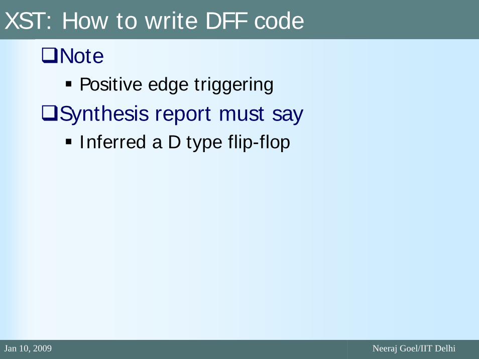
XST: How to write DFF code
Source: XST user guide, Xilinx.com
Jan 10, 2009 Neeraj Goel/IIT Delhi
XST: How to write DFF codeNote
Positive edge triggering
Synthesis report must sayInferred a D type flip-flop

Jan 10, 2009 Neeraj Goel/IIT Delhi
XST: How to write counter code
Source: XST user guide, Xilinx.com

Jan 10, 2009 Neeraj Goel/IIT Delhi
XST: How to write adder code
Source: XST user guide, Xilinx.com

Jan 10, 2009 Neeraj Goel/IIT Delhi
XST: How to write multiplier code
Source: XST user guide, Xilinx.com

Jan 10, 2009 Neeraj Goel/IIT Delhi
SummaryPresent day FPGAs are quite powerfulNeed to understand their strengths and internal characteristics to fully exploit their potentialDesigner must understand what will be designed
Apart from functional correctness, insight in structure is necessary for optimization If the implemented output is not desired
– Something wrong– EDA tools is not provided enough information!
Good to have understanding of tool flow for advanced manipulations

Jan 10, 2009 Neeraj Goel/IIT Delhi
Questions?
Jan 10, 2009 Neeraj Goel/IIT Delhi
Thank you!