Foundry fabricated photonic integrated circuit optical...
10
Foundry fabricated photonic integrated circuit optical phase lock loop KATARZYNA BAŁAKIER, 1,* MARTYN J. FICE, 1 LALITHA PONNAMPALAM, 1 CHRIS S. GRAHAM, 1 ADRIAN WONFOR, 2 ALWYN J. SEEDS, 1 AND CYRIL C. RENAUD 1 1 Department of Electronic and Electrical Engineering, University College London, WC1E 7JE, UK 2 Centre for Photonic Systems, Department of Engineering, University of Cambridge, CB3 0FA, UK * [email protected] Abstract: This paper describes the first foundry-based InP photonic integrated circuit (PIC) designed to work within a heterodyne optical phase locked loop (OPLL). The PIC and an external electronic circuit were used to phase-lock a single-line semiconductor laser diode to an incoming reference laser, with tuneable frequency offset from 4 GHz to 12 GHz. The PIC contains 33 active and passive components monolithically integrated on a single chip, fully demonstrating the capability of a generic foundry PIC fabrication model. The electronic part of the OPLL consists of commercially available RF components. This semi-packaged system stabilizes the phase and frequency of the integrated laser so that an absolute frequency, high- purity heterodyne signal can be generated when the OPLL is in operation, with phase noise lower than −100 dBc/Hz at 10 kHz offset from the carrier. This is the lowest phase noise level ever demonstrated by monolithically integrated OPLLs. Published by The Optical Society under the terms of the Creative Commons Attribution 4.0 License. Further distribution of this work must maintain attribution to the author(s) and the published article’s title, journal citation, and DOI. OCIS codes: (250.5300) Photonic integrated circuits; (130.0250) Optoelectronics; (130.3120) Integrated optics devices; (040.2840) Heterodyne; (060.5625) Radio frequency photonics; (140.3425) Laser stabilization. References and links 1. L. H. Enloe and J. L. Rodda, “Laser phase-locked loop,” Proc. IEEE 53(2), 165–166 (1964). 2. J. L. Hall, M. A. Long-sheng, and G. Kramer, “Principles of optical phase-locking : application to internal mirror He-Ne lasers phase-locked via fast control of the discharge current,” J. Quantum Electron. 23(4), 427–437 (1987). 3. W. R. Leeb, H. K. Philipp, A. L. Scholtz, and E. Bonek, “Frequency synchronization and phase locking of CO2 lasers,” Appl. Phys. Lett. 41(7), 592–594 (1982). 4. M. C. Amann and J. Buus, Tuneable Laser Diodes (Artech House, 1998). 5. J. Harrison and A. Mooradian, “Linewidth and offset frequency locking of external cavity GaAlAs lasers,” J. Quantum Electron. 25(6), 1152–1155 (1989). 6. R. T. Ramos and A. J. Seeds, “Fast heterodyne optical phase-lock loop using double quantum well laser diodes,” Electron. Lett. 28(1), 82–83 (1992). 7. R. J. Steed, L. Ponnampalam, M. J. Fice, C. C. Renaud, D. C. Rogers, D. G. Moodie, G. D. Maxwell, I. F. Lealman, M. J. Robertson, L. Pavlovic, L. Naglic, M. Vidmar, and A. J. Seeds, “Hybrid integrated optical phase- lock loops for photonic terahertz sources,” IEEE J. Sel. Top. Quantum Electron. 17(1), 210–217 (2011). 8. H. C. Park, M. Lu, E. Bloch, T. Reed, Z. Griffith, L. Johansson, L. Coldren, and M. Rodwell, “40Gbit/s coherent optical receiver using a Costas loop,” Opt. Express 20(26), B197–B203 (2012). 9. M. Lu, H.-C. Park, A. Sivananthan, J. S. Parker, E. Bloch, L. Johansson, M. J. W. Rodwell, and L. Coldren, “Monolithic Integration of a High-Speed Widely Tunable Optical Coherent Receiver,” IEEE Photonics Technol. Lett. 25(11), 1077–1080 (2013). 10. M. Lu, H. Park, E. Bloch, A. Sivananthan, A. Bhardwaj, Z. Griffith, L. A. Johansson, M. J. Rodwell, and L. A. Coldren, “Highly integrated optical heterodyne phase-locked loop with phase/frequency detection,” Opt. Express 20(9), 9736–9741 (2012). 11. K. Balakier, M. J. Fice, L. Ponnampalam, A. J. Seeds, and C. C. Renaud, “Monolithically integrated optical phase lock loop for microwave photonics,” J. Lightwave Technol. 32(20), 3893–3900 (2014). 12. A. J. Seeds, M. J. Fice, K. Balakier, M. Natrella, O. Mitrofanov, M. Lamponi, M. Chtioui, F. van Dijk, M. Pepper, G. Aeppli, A. G. Davies, P. Dean, E. Linfield, and C. C. Renaud, “Coherent terahertz photonics,” Opt. Express 21(19), 22988–23000 (2013). 13. P. H. Siegel, “Terahertz technology,” IEEE Trans. Microw. Theory Tech. 50(3), 910–928 (2002). Vol. 25, No. 15 | 24 Jul 2017 | OPTICS EXPRESS 16888 #286090 https://doi.org/10.1364/OE.25.016888 Journal © 2017 Received 3 Feb 2017; accepted 19 May 2017; published 10 Jul 2017
Transcript of Foundry fabricated photonic integrated circuit optical...

Foundry fabricated photonic integrated circuit optical phase lock loop KATARZYNA BAŁAKIER,1,* MARTYN J. FICE,1 LALITHA PONNAMPALAM,1 CHRIS S. GRAHAM,1 ADRIAN WONFOR,2 ALWYN J. SEEDS,1 AND CYRIL C. RENAUD1 1Department of Electronic and Electrical Engineering, University College London, WC1E 7JE, UK 2Centre for Photonic Systems, Department of Engineering, University of Cambridge, CB3 0FA, UK *[email protected]
Abstract: This paper describes the first foundry-based InP photonic integrated circuit (PIC) designed to work within a heterodyne optical phase locked loop (OPLL). The PIC and an external electronic circuit were used to phase-lock a single-line semiconductor laser diode to an incoming reference laser, with tuneable frequency offset from 4 GHz to 12 GHz. The PIC contains 33 active and passive components monolithically integrated on a single chip, fully demonstrating the capability of a generic foundry PIC fabrication model. The electronic part of the OPLL consists of commercially available RF components. This semi-packaged system stabilizes the phase and frequency of the integrated laser so that an absolute frequency, high-purity heterodyne signal can be generated when the OPLL is in operation, with phase noise lower than −100 dBc/Hz at 10 kHz offset from the carrier. This is the lowest phase noise level ever demonstrated by monolithically integrated OPLLs. Published by The Optical Society under the terms of the Creative Commons Attribution 4.0 License. Further distribution of this work must maintain attribution to the author(s) and the published article’s title, journal citation, and DOI.
OCIS codes: (250.5300) Photonic integrated circuits; (130.0250) Optoelectronics; (130.3120) Integrated optics devices; (040.2840) Heterodyne; (060.5625) Radio frequency photonics; (140.3425) Laser stabilization.
References and links 1. L. H. Enloe and J. L. Rodda, “Laser phase-locked loop,” Proc. IEEE 53(2), 165–166 (1964). 2. J. L. Hall, M. A. Long-sheng, and G. Kramer, “Principles of optical phase-locking : application to internal mirror
He-Ne lasers phase-locked via fast control of the discharge current,” J. Quantum Electron. 23(4), 427–437(1987).
3. W. R. Leeb, H. K. Philipp, A. L. Scholtz, and E. Bonek, “Frequency synchronization and phase locking of CO2lasers,” Appl. Phys. Lett. 41(7), 592–594 (1982).
4. M. C. Amann and J. Buus, Tuneable Laser Diodes (Artech House, 1998). 5. J. Harrison and A. Mooradian, “Linewidth and offset frequency locking of external cavity GaAlAs lasers,” J.
Quantum Electron. 25(6), 1152–1155 (1989).6. R. T. Ramos and A. J. Seeds, “Fast heterodyne optical phase-lock loop using double quantum well laser diodes,”
Electron. Lett. 28(1), 82–83 (1992).7. R. J. Steed, L. Ponnampalam, M. J. Fice, C. C. Renaud, D. C. Rogers, D. G. Moodie, G. D. Maxwell, I. F.
Lealman, M. J. Robertson, L. Pavlovic, L. Naglic, M. Vidmar, and A. J. Seeds, “Hybrid integrated optical phase-lock loops for photonic terahertz sources,” IEEE J. Sel. Top. Quantum Electron. 17(1), 210–217 (2011).
8. H. C. Park, M. Lu, E. Bloch, T. Reed, Z. Griffith, L. Johansson, L. Coldren, and M. Rodwell, “40Gbit/s coherent optical receiver using a Costas loop,” Opt. Express 20(26), B197–B203 (2012).
9. M. Lu, H.-C. Park, A. Sivananthan, J. S. Parker, E. Bloch, L. Johansson, M. J. W. Rodwell, and L. Coldren, “Monolithic Integration of a High-Speed Widely Tunable Optical Coherent Receiver,” IEEE Photonics Technol. Lett. 25(11), 1077–1080 (2013).
10. M. Lu, H. Park, E. Bloch, A. Sivananthan, A. Bhardwaj, Z. Griffith, L. A. Johansson, M. J. Rodwell, and L. A.Coldren, “Highly integrated optical heterodyne phase-locked loop with phase/frequency detection,” Opt. Express20(9), 9736–9741 (2012).
11. K. Balakier, M. J. Fice, L. Ponnampalam, A. J. Seeds, and C. C. Renaud, “Monolithically integrated optical phase lock loop for microwave photonics,” J. Lightwave Technol. 32(20), 3893–3900 (2014).
12. A. J. Seeds, M. J. Fice, K. Balakier, M. Natrella, O. Mitrofanov, M. Lamponi, M. Chtioui, F. van Dijk, M. Pepper, G. Aeppli, A. G. Davies, P. Dean, E. Linfield, and C. C. Renaud, “Coherent terahertz photonics,” Opt. Express 21(19), 22988–23000 (2013).
13. P. H. Siegel, “Terahertz technology,” IEEE Trans. Microw. Theory Tech. 50(3), 910–928 (2002).
Vol. 25, No. 15 | 24 Jul 2017 | OPTICS EXPRESS 16888
#286090 https://doi.org/10.1364/OE.25.016888 Journal © 2017 Received 3 Feb 2017; accepted 19 May 2017; published 10 Jul 2017

14. S. Hisatake, J. Y. Kim, K. Ajito, and T. Nagatsuma, “Self-heterodyne spectrometer using uni-traveling-carrier photodiodes for terahertz-wave generators and optoelectronic mixers,” J. Lightwave Technol. 32(20), 3683–3689 (2014).
15. M. Smit, X. Leijtens, E. Bente, J. Van der Tol, H. Ambrosius, D. Robbins, M. Wale, N. Grote, and M. Schell, “Generic foundry model for InP-based photonics,” IET Optoelectron. 5(5), 187–194 (2011).
16. M. Smit, X. Leijtens, H. Ambrosius, E. Bente, J. van der Tol, B. Smalbrugge, T. de Vries, E.-J. Geluk, J. Bolk, R. van Veldhoven, L. Augustin, P. Thijs, D. D’Agostino, H. Rabbani, K. Lawniczuk, S. Stopinski, S. Tahvili, A. Corradi, E. Kleijn, D. Dzibrou, M. Felicetti, E. Bitincka, V. Moskalenko, J. Zhao, R. Santos, G. Gilardi, W. Yao, K. Williams, P. Stabile, P. Kuindersma, J. Pello, S. Bhat, Y. Jiao, D. Heiss, G. Roelkens, M. Wale, P. Firth, F. Soares, N. Grote, M. Schell, H. Debregeas, M. Achouche, J.-L. Gentner, A. Bakker, T. Korthorst, D. Gallagher, A. Dabbs, A. Melloni, F. Morichetti, D. Melati, A. Wonfor, R. Penty, R. Broeke, B. Musk, and D. Robbins, “An introduction to InP-based generic integration technology,” Semicond. Sci. Technol. 29(8), 083001 (2014).
17. Photonic Advanced Research And Development for Integrated Generic Manufacturing (PARADIGM), “Web source,” http://www.paradigm.jeppix.eu/.
18. R. T. Ramos and A. J. Seeds, “Delay, linewidth and bandwidth limitations in optical phase-locked loop design,” Electron. Lett. 3(6), 389–391 (1990).
19. M. A. Grant, W. C. Michie, and M. J. Fletcher, “The performance of optical phase-locked loops in the presence of nonnegligible loop propagation delay,” J. Lightwave Technol. 5(4), 592–597 (1987).
20. PARADIGM Run 3, PARADIGM/EuroPIC Design Manual (2013). 21. R. Ulrich, “Image formation by phase coincidences in optical waveguides,” Opt. Commun. 13(3), 259–264
(1975). 22. L. B. Soldano and E. C. M. Pennings, “Optical multi-mode interference devices based on self-imaging:
principles and applications,” J. Lightwave Technol. 13(4), 615–627 (1995). 23. T. Okoshi, K. Kikuchi, and A. Nakayama, “Novel method for high resolution measurement of laser output
spectrum,” Electron. Lett. 16(16), 630–631 (1980). 24. A. J. Ward, G. Busico, N. D. Whitbread, L. Ponnampalam, J. P. Duck, and D. J. Robbins, “Linewidth in Widely
Tunable Digital Supermode Distributed Bragg Reflector Lasers: Comparison Between Theory and Measurement,” J. Quantum Electron. 42(11), 1122–1127 (2006).
25. N. Whitbread, A. Ward, L. Ponnampalam, and D. Robbins, “Digital wavelength selected DBR laser [invited paper],” Proc. SPIE 4995, 81–93 (2003).
26. L. Ponnampalam, M. Fice, F. Pozzi, C. Renaud, D. Rogers, I. F. Lealman, D. G. Moodie, P. J. Cannard, C. Lynch, L. Johnston, M. J. Robertson, R. Cronin, L. Pavlovic, L. Naglic, M. Vidmar, and A. Seeds, “Monolithically integrated photonic heterodyne system,” J. Lightwave Technol. 29(15), 2229–2234 (2011).
27. U. Gliese, E. L. Christensen, and K. E. Stubkjaer, “Laser linewidth requirements and improvements for coherent optical beam forming networks in satellites,” J. Lightwave Technol. 9(6), 779–790 (1991).
28. S. Kurtz, “Mixers as phase detectors,” Watkins Johnson Tech. Notes (1978). 29. R. J. Steed, F. Pozzi, M. J. Fice, C. C. Renaud, D. C. Rogers, I. F. Lealman, D. G. Moodie, P. J. Cannard, C.
Lynch, L. Johnston, M. J. Robertson, R. Cronin, L. Pavlovic, L. Naglic, M. Vidmar, and A. J. Seeds, “Monolithically integrated heterodyne optical phase-lock loop with RF XOR phase detector,” Opt. Express 19(21), 20048–20053 (2011).
1. Introduction Optical phase lock loops (OPLL) have been studied for decades resulting in numerous demonstrations of homodyne [1] and subsequently heterodyne [2] laser phase locking through the implementation of an electronic feedback loop. The very first experiments were based on gas lasers [3], which due to their narrow-linewidth enabled the loops to operate with long loop delay. However, these systems were limited by their lack of tuneability and compactness. The development of semiconductor laser diodes [4] led to a more compact and tuneable solution, however their wider linewidth and higher frequency instabilities [5] required a broadband phase lock loop circuit and short loop delay. To alleviate these limitations, hybrid integrated OPLLs [6, 7] were demonstrated. More recent progress in both photonic and electronic integration has resulted in monolithically integrated OPLLs, with particularly small dimensions, operating as homodyne [8, 9] or heterodyne [10, 11] systems. The compactness of such phase-locked optical sources is of particular interest due to numerous applications in optical communication, spectroscopy and high-frequency, high-purity signal generation through heterodyning [12]. OPLLs have proven useful in such applications as coherent optical communication, where they can be used to generate channel offset in dense wavelength division multiplexing or frequency down-conversion, where the slave laser is locked to the incoming signal before it is converted from the optical to the RF domain. Another interesting application is the synthesis of high-purity, broadly tuneable mm-wave or THz frequency signals. For this purpose the OPLL can
Vol. 25, No. 15 | 24 Jul 2017 | OPTICS EXPRESS 16889

be used as a very narrow bandwidth optical filter able to select and amplify a single line out of an optical frequency comb [12]. Furthermore, high-resolution THz frequency domain spectroscopy could also benefit from compact OPLL sub-systems [13, 14].
The continuous improvement of InP-based epitaxial growth and fabrication technologies has recently led to the development of the generic foundry photonic integration concept [15]. This approach allows numerous integrated circuits from different designers to be fabricated at the same time on a multi-project wafer using a generic fabrication process [16]. Thanks to this approach, both the time required to realize a prototype and the overall cost can be reduced significantly.
The first foundry-based OPLL photonic integrated circuit (PIC), presented in this paper, took full advantage of these developments. From the experimental foundry facilities developed by Oclaro UK, low-cost and compact phase locked sources have been developed in the context of a European research project [17]. The low cost of such systems is demonstrated, in particular, by the electronic part of the loop, which was designed to use off-the-shelf commercial components. Although the design is relatively simple to implement, high performance with phase noise reduced to lower than −100 dBc/Hz at 10 kHz offset is exhibited.
2. OPLL operation The concept of OPLL operation has already been discussed in several publications and the greatest challenge in realising an OPLL based on a semiconductor laser, which is the trade-off between the laser linewidth and loop propagation delay, has been explained [18, 19]. To control the phase noise of a wide linewidth laser, a loop with sufficiently wide bandwidth, hence small delay, is required. For instance, a laser with 1.2 MHz linewidth can be phase-stabilised to a reference source if the propagation delay in the feedback loop is less than 2.4 nanoseconds (assuming phase-error variance of 0.03 rad2 and reference laser linewidth of 50 kHz) [11].
For the circuit developed within this work, Fig. 1 shows the schematic of the OPLL architecture together with the experimental arrangement used during the laser phase locking demonstration. In particular, the laser on the chip was a distributed Bragg reflector (DBR) laser, offering 8 nm tuning, that included a phase section (PS) that was used as part of the feedback loop. The heterodyne between the reference laser and the integrated DBR laser was detected by a photodiode (PD) the output of which was amplified and sent to the phase detector to be compared with the RF reference, so providing the baseband phase-error signal.
Fig. 1. Schematic diagram of the optical phase lock loop experimental assembly.
2.1 PIC assembly
The PIC die was accommodated in the centre of an aluminium nitride submount, together with two alumina boards, one on each side of the chip. This allowed easy access to all integrated devices during characterisation and assembly of the electronic feedback loop. The PIC has been designed for direct wire bonding to 100-300 µm long rectangular DC current pads and round RF bond pads of 70 µm diameter (metal layer). All components with RF pads are located close to the edge of the chip, so that short bond wires can be used for connections to coplanar
Vol. 25, No. 15 | 24 Jul 2017 | OPTICS EXPRESS 16890

waveguide lines on the intermediate alumina board. The transmission parameters of the coplanar waveguides on the alumina tiles were measured to account for their effect on the loop gain and propagation time. The measured −3dB bandwidth was 30 GHz and the propagation delay was 24 ps. Subsequently, an interface PCB was attached at the other end of the alumina board to facilitate electrical connections through a 2 × 12 square pin header for DC currents and SMA connectors for RF signals. The circuitry for laser PS biassing and surface mount bias-tees to provide bias to PDs on the PIC were also implemented on this intermediate PCB. The −3dB bandwidth of PD and PS electrical connection paths located on the interface board were measured to be 16 GHz and 2 GHz, respectively. The total propagation delay related to the interface board was 600 ps. Lastly, to provide electrical connections, the gold pads on the PIC were wire-bonded to tracks on the alumina boards and subsequently from the alumina board onto the interface PCBs.
3. Design and characterisation of photonic integrated circuit The OPLL PIC fabrication was carried out on n-doped InP wafer, which was thinned to 135 μm ( ± 15 μm) before the n-contact metal was deposited. A single chip is 2 mm × 6 mm in size and contains a total of 33 components, including active and passive structures. Figure 2 shows a picture of the fabricated OPLL chip, which could be used to realize up to 3 individual OPLLs, depending on the configuration of the electrical connections.
Fig. 2. Photographs of OPLL PIC with dimensions of 2 mm x 6 mm. All components that do not form part of the OPLL are greyed out, so that the laser and photodiodes used in this experiment are more clearly visible.
3.1 Optical interconnections
One of the key design goals of the PIC was to decrease the losses related to light coupling to and guiding on the PIC. For that reason various types of photonic interconnect have been implemented to couple light efficiently between the laser and photodiode integrated on the chip, including couplers/splitters, optical waveguide and transition elements. Single-mode optical waveguides with strong (deep-etched) ridge (SR) and weak (shallow-etched) ridge (WR) were included in the design. Transmission loss of a typical 1.5 μm wide SR waveguide was specified to be 6–8 dB cm−1 for 1550 nm TE polarised light [20]. On that account the optical connection between the DBR laser and PD has been made short (< 1.2 mm) to reduce the loss as well as the propagation delay within feedback loop.
The PIC layout required curved optical waveguides, for which smaller radii require less space but are more prone to radiation losses. In this work, bend radii of 150 μm were repeatedly used for the SR waveguides. Furthermore, when the optical path consists of both SR and WR waveguides, 29 μm long transition tapers, with a flare angle of 0.5°, are implemented to match the waveguide width difference. Splitters and couplers used in the OPLL PIC are based on multimode interference (MMI) effects which rely on the multimode waveguide property of self-imaging [21]. The 2 × 2 MMI couplers offer superior performance in terms of wide optical bandwidth, low loss, insignificant polarisation dependence and relaxed fabrication requirements when compared to alternative solutions such as Y-junctions or directional couplers [22].
Vol. 25, No. 15 | 24 Jul 2017 | OPTICS EXPRESS 16891

3.2 Semiconductor laser diode
The semiconductor laser to be used in the OPLL should have good static spectral properties, such as wavelength that matches that of the reference laser and a narrow linewidth. Moreover, the FM characteristic, including the tuning sensitivity, flatness and bandwidth of the FM response of the laser should be well characterized to assess if the laser is suitable for use in the OPLL. Finally the laser tuneability should be adequate for the application.
The OPLL described in this paper is based on a DBR weak-ridge waveguide structure laser. The laser consist of four sections that include a multi-quantum well (MQW) section to provide gain, a phase control section and two identical mode-selective grating filters with 60% reflectivity, one at the front and one at the rear of the laser, as shown in Fig. 3. The laser gratings were written by e-beam lithography and their layer position and thickness leads to a coupling strength of ~50 cm−1. Each laser section is controlled with a separate electrode and electrically isolated from adjacent contacts by 10 μm-long isolation slots of weak passive waveguide structure. This is intended to provide around 1 k Ω electrical isolation [20]. The DBR laser has thresholds of approximately 12 mA and wavelength centered at approximately 1.53 µm. Furthermore, an integrated semiconductor optical amplifier (SOA) was implemented at the output of the DBR laser, with the aim of enhancing the optical signal before it was coupled to the optical fibre.
Fig. 3. Schematic (a) and photograph (b) of the DBR laser with wirebonded pads.
The linewidth of the DBR laser is a key characteristic as it defines the required OPLL bandwidth and, therefore, the allowable propagation delay within the loop [11]. A self-heterodyne interferometer technique with 5 km delay optical path [23] was used to measure the laser linewidth. During the measurement, only the laser gain section (70 mA) and SOA (5 mA) currents were applied, while no current was applied to the tuning sections. This was done to avoid line shape change in the presence of additional electrical noise in the tuning section currents [24, 25]. The measured self-heterodyne signal matched a 2.5 MHz FWHM Lorentzian line shape, suggesting that the linewidth of the DBR laser is 1.25 MHz.
The second key property of the laser is the PS tuning sensitivity and FM response, as these form part of the loop transfer function. The DBR laser PS can be used through current tuning for fine wavelength adjustment of up to 0.4 nm (50 GHz). The laser PS tuning sensitivity was measured to be up to −0.35 nm/mA (45 GHz/mA), offering a value that is sufficient for the overall gain in the loop [11]. The FM response of the laser was also characterised and measured and had a 3dB bandwidth of 100 MHz which will limit the overall achievable bandwidth of the feedback loop.
3.3 Photodiode
Among the key elements integrated into the PIC for the phase lock loop implementation are five side-illuminated waveguide PIN photodiodes that should offer bandwidth above 10 GHz, which is sufficient not to limit the loop gain and heterodyne capabilities. Each PD structure is fabricated in a deep-etched waveguide and PD is 50 µm long to ensure high absorption. The absorber is the same MQW layer stack as used for the laser gain section and SOA. To enable their efficient operation in the GHz range, the PDs were biased at −9V (Fig. 4) producing up to 5 mA of photocurrent when illuminated with the integrated DBR laser. Superior performance of the presented OPLL PIC is demonstrated by considering that the photocurrent generated by
Vol. 25, No. 15 | 24 Jul 2017 | OPTICS EXPRESS 16892
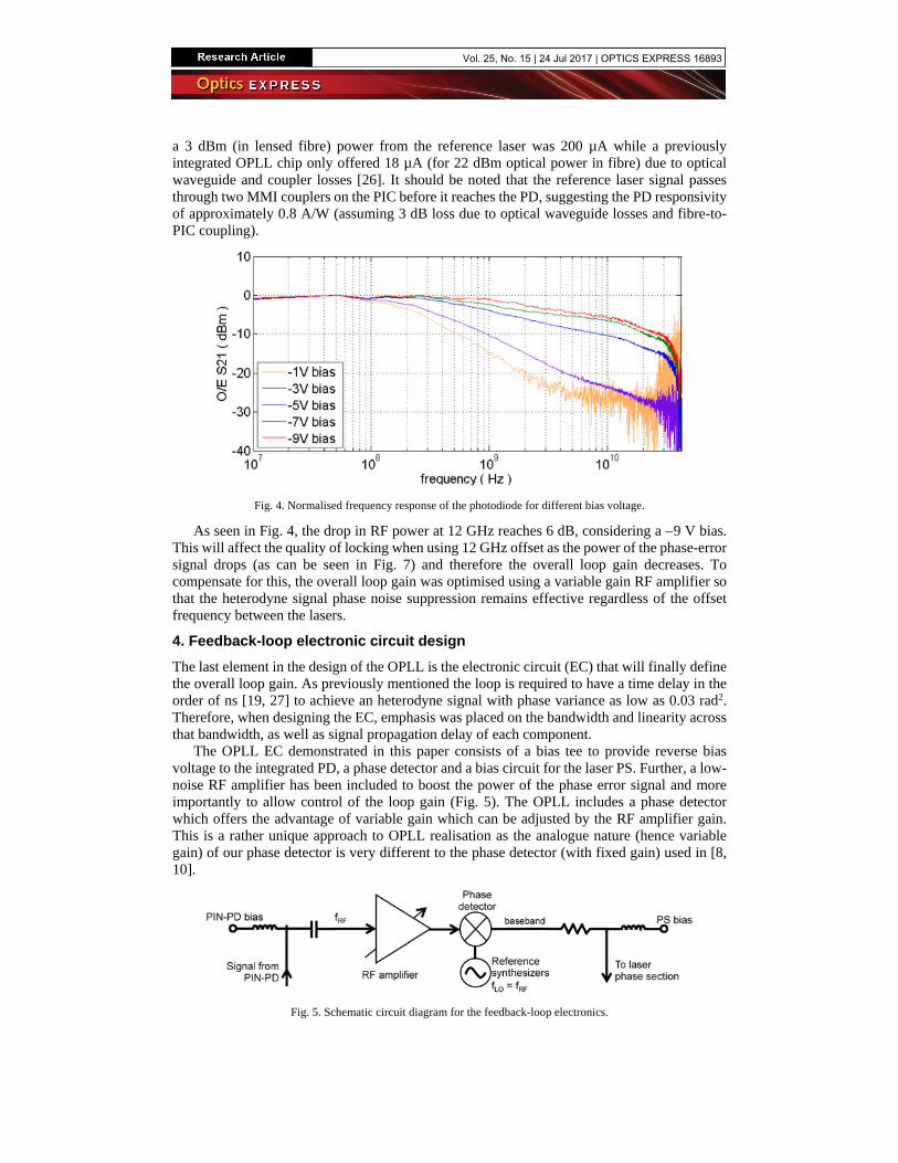
a 3 dBm (in lensed fibre) power from the reference laser was 200 µA while a previously integrated OPLL chip only offered 18 µA (for 22 dBm optical power in fibre) due to optical waveguide and coupler losses [26]. It should be noted that the reference laser signal passes through two MMI couplers on the PIC before it reaches the PD, suggesting the PD responsivity of approximately 0.8 A/W (assuming 3 dB loss due to optical waveguide losses and fibre-to-PIC coupling).
Fig. 4. Normalised frequency response of the photodiode for different bias voltage.
As seen in Fig. 4, the drop in RF power at 12 GHz reaches 6 dB, considering a −9 V bias. This will affect the quality of locking when using 12 GHz offset as the power of the phase-error signal drops (as can be seen in Fig. 7) and therefore the overall loop gain decreases. To compensate for this, the overall loop gain was optimised using a variable gain RF amplifier so that the heterodyne signal phase noise suppression remains effective regardless of the offset frequency between the lasers.
4. Feedback-loop electronic circuit design The last element in the design of the OPLL is the electronic circuit (EC) that will finally define the overall loop gain. As previously mentioned the loop is required to have a time delay in the order of ns [19, 27] to achieve an heterodyne signal with phase variance as low as 0.03 rad2. Therefore, when designing the EC, emphasis was placed on the bandwidth and linearity across that bandwidth, as well as signal propagation delay of each component.
The OPLL EC demonstrated in this paper consists of a bias tee to provide reverse bias voltage to the integrated PD, a phase detector and a bias circuit for the laser PS. Further, a low-noise RF amplifier has been included to boost the power of the phase error signal and more importantly to allow control of the loop gain (Fig. 5). The OPLL includes a phase detector which offers the advantage of variable gain which can be adjusted by the RF amplifier gain. This is a rather unique approach to OPLL realisation as the analogue nature (hence variable gain) of our phase detector is very different to the phase detector (with fixed gain) used in [8, 10].
Fig. 5. Schematic circuit diagram for the feedback-loop electronics.
Vol. 25, No. 15 | 24 Jul 2017 | OPTICS EXPRESS 16893

The gain of this low-noise (noise figure < 2 dB) control amplifier is adjusted between 15 and 30 dB by control voltage, and the gain flatness is +/− 3 dB within the frequency operation range of 2 to 16 GHz. The RF amplifier contributes 350 ps to the total loop delay.
In the OPLL EC, the phase detector is a commercially available SMA connectorised double-balanced mixer. This device offers wide bandwidth 4-12 GHz, low conversion loss (7dB), short delay of 310 ps and high isolation between the ports of 45 dB. The high isolation of 45 dB between the mixer ports is particularly important since it is inversely proportional to the DC voltage offset at the IF port [28]. The DC offset level at the IF port of the chosen phase detector was measured to be less than 2 mV when driven by an LO signal between 7 dBm and 12 dBm, as would be expected [28].
All the elements of the loop then enabled a compact OPLL circuit with a simple electronic circuit that offers potential heterodyne tuning from 4 to 12 GHz, gain control, a loop bandwidth of 100 MHz and a total loop delay of 1.8 ns (less than the 2.4 ns required for 0.03 rad2 phase error variance). The OPLL is a 1st order loop and was designed to have 47 deg of phase margin.
5. Phase locking experiment results and discussion The schematic of the OPLL and test assembly was presented in Fig. 1. During the experiment the reference laser was coupled to the PIC through a lensed fibre aligned to the optical waveguide with spot size converter (Fig. 2.). The reference optical signal is guided on the ridge waveguide into a 2 × 2 MMI coupler which combines the incoming and integrated laser signals and splits these signals between two waveguides connected to the pair of PDs that converts the heterodyne signal from the optical to the electrical domain. One of the PD pairs is used to detect the phase-error signal processed by the feedback loop, while the other is used for lock monitoring purposes. The output of the monitoring PD is connected to an electrical spectrum analyser (ESA) where the beat note between the two lasers can be observed and the quality of locking can be assessed. The measured heterodyne is presented in Fig. 6, demonstrating the difference in linewidth and peak power of the free running and locked signal for a 8 GHz offset.
Fig. 6. Electrical spectra of the phase locked and free running heterodyne signal. RBW = 300 kHz, VBW = 30 kHz, SWT = 0.09s. Measurements present 50 sweeps in max-hold trace mode.
When the feedback loop was disabled, the linewidth of the free running heterodyne signal was in the tens of MHz range and the frequency jitter was over approximately 100 MHz range. This behaviour is due to the combined linewidth and wavelength fluctuation of the reference and DBR lasers, even though an external cavity laser with <100 kHz linewidth was used as a reference source.
Due to the loop design, the DBR laser can be phase locked to the incoming signal with any frequency offset between 4 GHz and 12 GHz, as shown in Fig. 7. The offset frequency is limited at the lower end by the bandwidth of the dual-balanced mixer used as the phase detector and at the higher frequency end by the bandwidth of the PD.
Vol. 25, No. 15 | 24 Jul 2017 | OPTICS EXPRESS 16894

The lock-in and hold-in range of this OPLL is about 200 MHz, which is the expected range for the 1st order type I loop, and could be increased by adding a pole into the loop transfer function, for instance by introducing a loop filter with an integrator function. This could also improve the long term thermal stability, which is currently controlled with a Peltier cooler. Moreover, adding or modifying the loop filter can be easily achieved given the OPLL consists of connectorised components.
Fig. 7. Electrical spectra of heterodyne signal measured at 4 GHz (a), 6 GHz (b), 10 GHz (b) and 12 GHz (d) frequency offset between the two lasers. RBW = 500 kHz, VBW = 100kHz.
To further assess the quality of phase locking, the single-sideband phase noise spectra of the heterodyne signal were measured for two different loop gains. The phase noise achieved was below –100 dBc at 10 kHz frequency offset from the 8 GHz carrier (Fig. 8). This leads to a phase-error variance of the generated heterodyne signal to be as low as 0.012 rad2 for offsets between 1 kHz to 1 GHz, for the plot with lower loop gain in Fig. 8. This is best phase noise suppression level ever demonstrated by the monolithically integrated OPLLs. The previous lowest phase noise was reported to be −90 dBc/Hz at 20 MHz offset from a 4 GHz carrier [29].
Vol. 25, No. 15 | 24 Jul 2017 | OPTICS EXPRESS 16895

Fig. 8. The SSB phase noise spectra of the phase locked heterodyne signal at 8 GHz.
Figure 8 also demonstrates the effect of loop gain variation and the importance of optimisation. Although, higher loop gain offer further phase noise reduction closer to the carrier a secondary peak becomes visible in the phase noise spectra that would potentially increase the overall phase variance. Furthermore, the measurements presented in Fig. 8 suggest the OPLL closed loop bandwidth to be about 100 MHz.
6. Conclusion We have demonstrated the first OPLL based on generic foundry-fabricated PIC and off-the-shelf electronic commercial components creating potentially a simpler overall circuit assembly than previous such systems. The OPLL demonstrated 100 MHz bandwidth and 8 GHz heterodyne tuning. The PIC, designed to offer DBR laser monolithically integrated with photodiode and low-loss optical interconnections, was successfully fabricated and demonstrated all the necessary performance to operate within an optical phase lock loop. This proves that generic foundry can be used to deliver PICs characterised by sufficient performance for selected applications at a fraction of the cost of a dedicated fabrication process. The feedback electronics is realised in a semi-packaged form, which means that all electrical connections (DC and RF) are connectorised. This creates potential for further improvements as substituting RF amplifier and phase detector with the surface mount equivalent would significantly reduce the 1.8 ns loop delay, allowing for grater loop bandwidth.
The overall simple design based on commercially available electronic components and foundry-based PICs offers a route to a simpler OPLL sub-system suitable for a number of applications. Despite the simple design, the assembled OPLL was characterised by state-of-the-art performance, with the on-chip DBR laser being phase stabilised to an external reference laser with 4 GHz - 12 GHz frequency offset. The SSB phase noise of the heterodyne was measured to be less than −100 dBc/Hz at 10 kHz offset from the 8 GHz carrier, resulting in phase-error variance of 0.012 rad2. This is the lowest residual phase noise level of the heterodyne signal ever reported in a monolithically integrated OPLL system.
Funding European Commission Seventh Framework Programme (FP7-ICT) through IPHOBAC-NG (619870) and PARADIGM (257210) projects; Engineering and Physical Sciences Research Council (EPSRC) through COTS project (EP/J017671/1).
Vol. 25, No. 15 | 24 Jul 2017 | OPTICS EXPRESS 16896

Acknowledgments The authors would like to acknowledge Mike Wale, Mark Kearley and team at Oclaro Technology, UK for their work on the PIC fabrication; Martin Scott from University College London for help with the interface board realisation.
Vol. 25, No. 15 | 24 Jul 2017 | OPTICS EXPRESS 16897