Foundation Series ISE 3.1i In-Depth Tutorial · UG101 (v1.0) July 21, 2000 iii Foundation Series...
94
R Foundation Series ISE 3.1i In-Depth Tutorial Watch Design UG101 (v1.0) July 21, 2000
Transcript of Foundation Series ISE 3.1i In-Depth Tutorial · UG101 (v1.0) July 21, 2000 iii Foundation Series...

R
Foundation Series ISE 3.1i In-Depth TutorialWatch Design
UG101 (v1.0) July 21, 2000

The Xilinx logo shown above is a registered trademark of Xilinx, Inc.
ASYL, FPGA Architect, FPGA Foundry, NeoCAD, NeoCAD EPIC, NeoCAD PRISM, NeoROUTE, Timing Wizard, TRACE, XACT, XILINX, XC2064, XC3090, XC4005, XC5210, and XC-DS501 are registered trademarks of Xilinx, Inc.
The shadow X shown above is a trademark of Xilinx, Inc.
All XC-prefix product designations, A.K.A Speed, Alliance Series, AllianceCORE, BITA, CLC, Configurable Logic Cell, CoolRunner, CORE Gen-erator, CoreLINX, Dual Block, EZTag, FastCLK, FastCONNECT, FastFLASH, FastMap, Fast Zero Power, Foundation, HardWire, IRL, LCA, Logi-
BLOX, Logic Cell, LogiCORE, LogicProfessor, MicroVia, MultiLINX, PLUSASM, PowerGuide, PowerMaze, QPro, RealPCI, RealPCI 64/66, SelectI/O, SelectRAM, SelectRAM+, Silicon Xpresso, Smartguide, Smart-IP, SmartSearch, Smartspec, SMARTSwitch, Spartan, TrueMap, UIM,
VectorMaze, VersaBlock, VersaRing, Virtex, WebFitter, WebLINX, WebPACK, XABEL, XACTstep, XACTstep Advanced, XACTstep Foundry, XACT-Floorplanner, XACT-Performance, XAM, XAPP, X-BLOX, X-BLOX plus, XChecker, XDM, XDS, XEPLD, Xilinx Foundation Series, XPP, XSI, and ZERO+ are trademarks of Xilinx, Inc. The Programmable Logic Company and The Programmable Gate Array Company are service
marks of Xilinx, Inc.
All other trademarks are the property of their respective owners.
Xilinx, Inc. does not assume any liability arising out of the application or use of any product described or shown herein; nor does it convey any license under its patents, copyrights, or maskwork rights or any rights of others. Xilinx, Inc. reserves the right to make changes, at any time, in order to improve reliability, function or design and to supply the best product possible. Xilinx, Inc. will not assume responsibility for the use of any circuitry described herein other than circuitry entirely embodied in its products. Xilinx, Inc. devices and products are protected under one or more of the following U.S. Patents: 4,642,487; 4,695,740; 4,706,216; 4,713,557; 4,746,822; 4,750,155; 4,758,985; 4,820,937; 4,821,233; 4,835,418;
4,855,619; 4,855,669; 4,902,910; 4,940,909; 4,967,107; 5,012,135; 5,023,606; 5,028,821; 5,047,710; 5,068,603; 5,140,193; 5,148,390; 5,155,432; 5,166,858; 5,224,056; 5,243,238; 5,245,277; 5,267,187; 5,291,079; 5,295,090; 5,302,866; 5,319,252; 5,319,254; 5,321,704; 5,329,174; 5,329,181; 5,331,220; 5,331,226; 5,332,929; 5,337,255; 5,343,406; 5,349,248; 5,349,249; 5,349,250; 5,349,691; 5,357,153; 5,360,747; 5,361,229; 5,362,999; 5,365,125; 5,367,207; 5,386,154; 5,394,104; 5,399,924; 5,399,925; 5,410,189; 5,410,194; 5,414,377; 5,422,833; 5,426,378; 5,426,379; 5,430,687; 5,432,719; 5,448,181; 5,448,493; 5,450,021; 5,450,022; 5,453,706; 5,455,525; 5,466,117; 5,469,003; 5,475,253; 5,477,414; 5,481,206; 5,483,478; 5,486,707; 5,486,776; 5,488,316; 5,489,858; 5,489,866; 5,491,353; 5,495,196; 5,498,979; 5,498,989; 5,499,192; 5,500,608; 5,500,609; 5,502,000; 5,502,440; 5,504,439; 5,506,518; 5,506,523; 5,506,878; 5,513,124; 5,517,135; 5,521,835; 5,521,837; 5,523,963; 5,523,971; 5,524,097; 5,526,322; 5,528,169; 5,528,176; 5,530,378; 5,530,384; 5,546,018; 5,550,839; 5,550,843; 5,552,722; 5,553,001; 5,559,751; 5,561,367; 5,561,629; 5,561,631; 5,563,527; 5,563,528; 5,563,529; 5,563,827; 5,565,792; 5,566,123; 5,570,051; 5,574,634; 5,574,655; 5,578,946; 5,581,198; 5,581,199; 5,581,738; 5,583,450; 5,583,452; 5,592,105; 5,594,367; 5,598,424; 5,600,263; 5,600,264; 5,600,271; 5,600,597; 5,608,342; 5,610,536; 5,610,790; 5,610,829; 5,612,633; 5,617,021; 5,617,041; 5,617,327; 5,617,573; 5,623,387; 5,627,480; 5,629,637; 5,629,886; 5,631,577; 5,631,583; 5,635,851; 5,636,368; 5,640,106; 5,642,058; 5,646,545; 5,646,547; 5,646,564; 5,646,903; 5,648,732; 5,648,913; 5,650,672; 5,650,946; 5,652,904; 5,654,631; 5,656,950; 5,657,290; 5,659,484; 5,661,660; 5,661,685; 5,670,896; 5,670,897; 5,672,966; 5,673,198; 5,675,262; 5,675,270; 5,675,589; 5,677,638; 5,682,107; 5,689,133; 5,689,516; 5,691,907; 5,691,912; 5,694,047; 5,694,056; 5,724,276; 5,694,399; 5,696,454; 5,701,091; 5,701,441; 5,703,759; 5,705,932; 5,705,938; 5,708,597; 5,712,579; 5,715,197; 5,717,340; 5,719,506; 5,719,507; 5,724,276; 5,726,484; 5,726,584; 5,734,866; 5,734,868; 5,737,234; 5,737,235; 5,737,631; 5,742,178; 5,742,531; 5,744,974; 5,744,979; 5,744,995; 5,748,942; 5,748,979; 5,752,006; 5,752,035; 5,754,459; 5,758,192; 5,760,603; 5,760,604; 5,760,607; 5,761,483; 5,764,076; 5,764,534; 5,764,564; 5,768,179; 5,770,951; 5,773,993; 5,778,439; 5,781,756; 5,784,313; 5,784,577; 5,786,240; 5,787,007; 5,789,938; 5,790,479; 5,790,882; 5,795,068; 5,796,269; 5,798,656; 5,801,546; 5,801,547; 5,801,548; 5,811,985; 5,815,004; 5,815,016; 5,815,404; 5,815,405; 5,818,255; 5,818,730; 5,821,772; 5,821,774; 5,825,202; 5,825,662; 5,825,787; 5,828,230; 5,828,231; 5,828,236; 5,828,608; 5,831,448; 5,831,460; 5,831,845; 5,831,907; 5,835,402; 5,838,167; 5,838,901; 5,838,954; 5,841,296; 5,841,867; 5,844,422; 5,844,424; 5,844,829; 5,844,844; 5,847,577; 5,847,579; 5,847,580; 5,847,993; 5,852,323; 5,861,761; 5,862,082; 5,867,396; 5,870,309; 5,870,327; 5,870,586; 5,874,834; 5,875,111; 5,877,632; 5,877,979; 5,880,492; 5,880,598; 5,880,620; 5,883,525; 5,886,538; 5,889,411; 5,889,413; 5,889,701; 5,892,681; 5,892,961; 5,894,420; 5,896,047; 5,896,329; 5,898,319; 5,898,320; 5,898,602; 5,898,618; 5,898,893; 5,907,245; 5,907,248; 5,909,125; 5,909,453; 5,910,732; 5,912,937; 5,914,514; 5,914,616; 5,920,201; 5,920,202; 5,920,223; 5,923,185; 5,923,602; 5,923,614; 5,928,338; 5,931,962; 5,933,023; 5,933,025; 5,933,369; 5,936,415; 5,936,424; 5,939,930; 5,942,913; 5,944,813; 5,945,837; 5,946,478; 5,949,690; 5,949,712; 5,949,983; 5,949,987; 5,952,839; 5,952,846; 5,955,888; 5,956,748; 5,958,026; 5,959,821; 5,959,881; 5,959,885; 5,961,576; 5,962,881; 5,963,048; 5,963,050; 5,969,539; 5,969,543; 5,970,142; 5,970,372; 5,971,595; 5,973,506; 5,978,260; 5,986,958; 5,990,704; 5,991,523;
5,991,788; 5,991,880; 5,991,908; 5,995,419; 5,995,744; 5,995,988; 5,999,014; 5,999,025; 6,002,282; and 6,002,991; Re. 34,363, Re. 34,444, and Re. 34,808. Other U.S. and foreign patents pending. Xilinx, Inc. does not represent that devices shown or products described herein are free from patent infringement or from any other third party right. Xilinx, Inc. assumes no obligation to correct any errors contained herein or to advise any user of this text of any correction if such be made. Xilinx, Inc. will not assume any liability for the accuracy or correctness of any engineering
or software support or assistance provided to a user.
Xilinx products are not intended for use in life support appliances, devices, or systems. Use of a Xilinx product in such applications without the written consent of the appropriate Xilinx officer is prohibited.
Copyright 1991-2000 Xilinx, Inc. All Rights Reserved.
R
Foundation Series ISE 3.1i In-Depth Tutorial www.xilinx.com UG101 (v1.0) July 21, 20001-800-255-7778

Foundation Series ISE 3.1i In-Depth TutorialUG101 (v1.0) July 21, 2000
The following table shows the revision history for this document.
Date Version Revision
06/01/00 1.0 Initial Xilinx release.
06/15/00 1.1 Accumulated miscellaneous updates and bug fixes.
UG101 (v1.0) July 21, 2000 www.xilinx.com Foundation Series ISE 3.1i In-Depth Tutorial1-800-255-7778

Foundation Series ISE 3.1i In-Depth Tutorial www.xilinx.com UG101 (v1.0) July 21, 20001-800-255-7778
Contents
PrefaceAbout the In-Depth Tutorials....................................................................................... vAdditional Resources ....................................................................................................... v
Quick Start Guide Contents ......................................................................................... vi
ConventionsTypographical .................................................................................................................... vii
Online Document............................................................................................................ viii
Chapter 1: HDL-Based DesignGetting Started .................................................................................................................... 1
Nomenclature ................................................................................................................... 1Required Software............................................................................................................ 2Installing the Tutorial ...................................................................................................... 2Tutorial Project Directories and Files ............................................................................ 2VHDL or Verilog? ............................................................................................................ 2Starting the Project Navigator ........................................................................................ 3Copying the Tutorial Files (Optional) ........................................................................... 3
Design Description ........................................................................................................... 3The Project Navigator ...................................................................................................... 4
Source Window ................................................................................................................ 5Process Window ............................................................................................................... 6Console Window.............................................................................................................. 6Snapshots........................................................................................................................... 8
XST or FPGA Express Synthesis ................................................................................. 8Xilinx Synthesis Technology (XST)................................................................................ 8FPGA Express ................................................................................................................... 8
Design Entry ......................................................................................................................... 9Adding Source Files......................................................................................................... 9Correcting HDL errors .................................................................................................. 10Starting the HDL Editor ................................................................................................ 10Creating an HDL-Based Module ................................................................................. 10Creating a CoreGEN Module ....................................................................................... 14
Synthesizing the Design with XST .......................................................................... 20Synthesizing the Design with FPGA Express ..................................................... 21
The Express Constraints Editor (FPGA Express Only) ................................... 21Using the Express Constraints Editor (FPGA Express Only) ....................... 22
Viewing Synthesis Results (FPGA Express Only) ............................................ 24
Chapter 2: Schematic-Based DesignGetting Started .................................................................................................................. 27
Nomenclature ................................................................................................................. 27Required Software.......................................................................................................... 27Installing the Tutorial .................................................................................................... 28Tutorial Project Directories and Files .......................................................................... 28
UG101 (v1.0) July 21, 2000 www.xilinx.com iFoundation Series ISE 3.1i In-Depth Tutorial 1-800-255-7778
R
Starting the Project Navigator ...................................................................................... 28Copying the Tutorial Files (Optional) ......................................................................... 29
Design Description ......................................................................................................... 29
The Project Navigator .................................................................................................... 31Source Window .............................................................................................................. 31Process Window ............................................................................................................. 33Console Window............................................................................................................ 33Snapshots......................................................................................................................... 33
XST or FPGA Express Synthesis ............................................................................... 34Xilinx Synthesis Technology (XST).............................................................................. 34FPGA Express ................................................................................................................. 34
Design Entry ....................................................................................................................... 34Starting the Schematic Editor ....................................................................................... 35Executing Commands ................................................................................................... 35Manipulating the Screen ............................................................................................... 36Creating a Schematic-Based Macro ............................................................................. 36Creating the CNT60 Schematic .................................................................................... 37Creating a CORE Generator Module .......................................................................... 43Creating the Core Generator Module ......................................................................... 44Creating a State Machine Module ............................................................................... 45Creating an HDL-Based Module ................................................................................. 53Specifying Device Inputs/Outputs ............................................................................. 57Adding I/O Markers and Net Names ........................................................................ 59Assigning Pin Locations................................................................................................ 60Completing the Schematic ............................................................................................ 61
Chapter 3: Functional SimulationStarting HDL Bencher.................................................................................................... 65
Creating Stimulas ........................................................................................................... 65Specifying Expected Response ..................................................................................... 66Creating a Test Bench .................................................................................................... 67Adding the Test Bench to the Project .......................................................................... 67
Starting Modelsim ........................................................................................................... 67Specifying Simulation Process Properties .................................................................. 68Performing Simulation .................................................................................................. 69
Adding Signals.................................................................................................................. 69
Saving the Simulation ................................................................................................... 70Restarting the Simulation ............................................................................................ 71
Chapter 4: Design ImplementationProject Management ....................................................................................................... 73
Starting Implementation .............................................................................................. 74Implemention Options .................................................................................................. 74Timing Report Generation ............................................................................................ 75Control Files .................................................................................................................... 76
Running Implementation............................................................................................. 76
Viewing Implementation Results ............................................................................ 77Other Implementation Tools ...................................................................................... 78
Chapter 5: Timing SimulationModifying the Test Bench ............................................................................................ 79Starting Modelsim ........................................................................................................... 79
Specifying Simulation Process Properties .................................................................. 79
ii www.xilinx.com UG101 (v1.0) July 21, 20001-800-255-7778 Foundation Series ISE 3.1i In-Depth Tutorial

R
Performing Simulation .................................................................................................. 80Adding Signals.................................................................................................................. 81
Saving the Simulation ................................................................................................... 82
UG101 (v1.0) July 21, 2000 www.xilinx.com iiiFoundation Series ISE 3.1i In-Depth Tutorial 1-800-255-7778

R
iv www.xilinx.com UG101 (v1.0) July 21, 20001-800-255-7778 Foundation Series ISE 3.1i In-Depth Tutorial

R
Preface
About the In-Depth TutorialsThese tutorials give a description of the features and additions to Xilinx’s newest product—Foundation ISE 3.1i. The primary focus of this tutorial is to show the relationship between the design entry tools and the design implementation tools.
This guide should be used as the initial learning tool for designers who are unfamiliar with the features of the Foundation iSE software.
Additional ResourcesFor additional information, go to http://support.xilinx.com. The following table lists some of the resources you can access from this page. You can also directly access some of these resources using the provided URLs.
Resource Description/URL
Tutorial Tutorials covering Xilinx design flows, from design entry to verification and debugging
http://support.xilinx.com/support/techsup/tutorials/index.htm
AnswersDatabase
Current listing of solution records for the Xilinx software toolsSearch this database using the search function at http://support.xilinx.com/support/searchtd.htm
Application Notes
Descriptions of device-specific design techniques and approaches
http://support.xilinx.com/apps/appsweb.htm
Data Book Pages from The Programmable Logic Data Book, which describe device-specific information on Xilinx device characteristics, including readback, boundary scan, configuration, length count, and debugging
http://support.xilinx.com/partinfo/databook.htm
Xcell Journals Quarterly journals for Xilinx programmable logic users
http://support.xilinx.com/xcell/xcell.htm
Tech Tips Latest news, design tips, and patch information on the Xilinx design environment
http://support.xilinx.com/support/techsup/journals/index.htm
UG101 (v1.0) July 21, 2000 www.xilinx.com vFoundation Series ISE 3.1i In-Depth Tutorial 1-800-255-7778

PrefaceR
Quick Start Guide ContentsThis guide covers the following topics.
• Chapter 1, “HDL-Based Design,” guides you through a typical HDL-based design procedure using a design of a runner ’s stopwatch called “Watch”.
• Chapter 2, “Schematic-Based Design,” explains many different facets of a schematic-based Foundation iSE design flow using a design of a runner ’s stopwatch called “Watch”. This chapter also shows how to use Foundation iSE accessories such as the StateCad, Project Navigator, LogiBLOX, and the HDL Editor.
• Chapter 3, “Functional Simulation,” explains how to use the Logic Simulator to simulate a design before design implementation to verify that the logic that you have created is correct.
• Chapter 4, “Design Implementation,” describes how to Translate, Map, Place, Route, (Fit for CPLDs) and generate a Bit file for designs.
• Chapter 5, “Timing Simulation,” explains how to perform a timing simulation using the block and routing delay information from the routed design to give an accurate assessment of the behavior of the circuit under worst-case conditions.
vi www.xilinx.com UG101 (v1.0) July 21, 20001-800-255-7778 Foundation Series ISE 3.1i In-Depth Tutorial

R
Conventions
This manual uses the following typographical and online document conventions. An example illustrates each typographical convention.
TypographicalThe following conventions are used for all documents.
• Courier font indicates messages, prompts, and program files that the system displays.
speed grade: -100
• Courier bold indicates literal commands that you enter in a syntactical statement. However, braces “{ }” in Courier bold are not literal and square brackets “[ ]” in Courier bold are literal only in the case of bus specifications, such as bus [7:0].
rpt_del_net=
Courier bold also indicates commands that you select from a menu.
File → Open
• Italic font denotes the following items.- Variables in a syntax statement for which you must supply values
- edif2ngd design_name
- References to other manuals
See the Development System Reference Guide for more information.- Emphasis in text
If a wire is drawn so that it overlaps the pin of a symbol, the two nets are not connected.
• Square brackets “[ ]” indicate an optional entry or parameter. However, in bus specifications, such as bus [7:0], they are required.
edif2ngd [option_name] design_name
• Braces “{ }” enclose a list of items from which you must choose one or more.
lowpwr ={on|off}
• A vertical bar “|” separates items in a list of choices.
lowpwr ={on|off}
UG101 (v1.0) July 21, 2000 www.xilinx.com viiFoundation Series ISE 3.1i In-Depth Tutorial 1-800-255-7778

ConventionsR
• A vertical ellipsis indicates repetitive material that has been omitted.
IOB #1: Name = QOUT’IOB #2: Name = CLKIN’...
• A horizontal ellipsis “. . .” indicates that an item can be repeated one or more times.
allow block block_name loc1 loc2 ... locn;
Online DocumentThe following conventions are used for online documents.
• Red-underlined text indicates an interbook link, which is a cross-reference to another book. Click the red-underlined text to open the specified cross-reference.
• Blue-underlined text indicates an intrabook link, which is a cross-reference within a book. Click the blue-underlined text to open the specified cross-reference.
viii www.xilinx.com UG101 (v1.0) July 21, 20001-800-255-7778 Foundation Series ISE 3.1i In-Depth Tutorial
R
Chapter 1
HDL-Based Design
This chapter guides you through a typical HDL-based design procedure using a design of a runner ’s stopwatch called Watch. The design example used in this tutorial demonstrates many device features, software features and design flow practices which you can apply to your own design. This design targets a Virtex device; however, all of the principles and flows taught are applicable to any Xilinx device family, unless otherwise noted.
For an example of how to design with CPLDs, see the online help by selecting Help → Foundation ISE Help Contents from the Project Navigator. Under Tutorials, select CPLD Design Flows.
The design is composed of HDL elements and a CORE Generator macro; you will synthesize the design using the Xilinx Synthesis Technology(XST) or FPGA Express.
Then, you will simulate the HDL code using the Modelsim Simulator. In the third part, you will implement the design using the Xilinx Implementation Tools. The simulation, implementation, and bitstream generation are described in subsequent chapters.
This chapter includes the following sections.
• “Getting Started”• “Design Description”
• “The Project Navigator”• “XST or FPGA Express Synthesis”
• “Design Entry”• “Synthesizing the Design with XST”
• “Synthesizing the Design with FPGA Express”• “The Express Constraints Editor (FPGA Express Only)”
• “Using the Express Constraints Editor (FPGA Express Only)”• “Viewing Synthesis Results (FPGA Express Only)”
Getting Started• The following subsections describe the basic requirements for running the tutorial.
NomenclatureIn this tutorial, the following terms are used:
• “Virtex™ family” includes the Virtex, Sparta®-II and Virtex-E devices only.• “Right-click” means click the right mouse button. Unless specified, all other mouse
operations are performed with the left mouse button.
Throughout this tutorial, file names, project names, and directory names (paths) are specified in lower case, and the design is referred to as Watch.
UG000 (v1.1) June 15, 2000 www.xilinx.com 1Templates for Xilinx User Guides 1-800-255-7778
Chapter 1: HDL-Based DesignR
Required SoftwareThe Xilinx Foundation Series ISE package, Version 3.1i, is required to perform this tutorial. The design requires that you have installed the Virtex libraries and device files and are licensed for FPGA Express or Base Express. You must also have the Watch projects which may be downloaded from http://support.xilinx.com.
Note: A Foundation Express license is required to access the Express Constraints GUI.
Installing the TutorialThis tutorial assumes that the software is installed in the default location C:\XILINX. If you have installed the software in a different location, substitute your installation path for C:\XILINX.
Unzip the tutorial projects in the C:\XILINX\ directory and replace any existing files. The files downloaded from the web have been updated.
Note: For detailed instructions, refer to the Foundation Series ISE 3.1i Install and Release Document.
Tutorial Project Directories and FilesThe WTUT_VHD and WTUT_VER directories are created within C:\XILINX\iSEexamples, and the tutorial files are copied into these directories. These directories contain complete and incomplete versions of the design, done in VHDL and Verilog, respectively. You will complete the design in the tutorial. However, solutions projects with all completed input and output files are also provided. The following table lists the associated project.
The WATCHVHD and WATCHVER solution projects contain the design files for the completed tutorials, including HDL files and the bitstream file.To conserve disk space, some intermediate files are not provided. Do not overwrite any files in the solutions directories.
The WTUT_VHD and WTUT_VER projects contain incomplete copies of the tutorial design. You will create the remaining files when you perform the tutorial. As described in a later step, you have the option to copy the Watch project to another area and perform the tutorial in this new area if desired.
VHDL or Verilog?This tutorial has been prepared for both VHDL and Verilog designs. This document applies to both designs simultaneously, noting differences where applicable. You will need to decide which HDL language you would like to work through the tutorial when you open the project.
Table 1: Tutorial Project Directories
Directory Description
WTUT_VHD Incomplete Watch Tutorial - VHDLWTUT_VER Incomplete Watch Tutorial - Verilog
WATCHVHD Solution for Watch - VHDLWATCHVER Solution for Watch - Verilog
2 www.xilinx.com UG000 (v1.1) June 15, 20001-800-255-7778 Templates for Xilinx User Guides
Chapter 1: HDL-Based DesignR
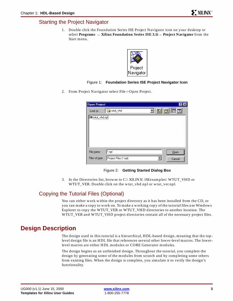
Starting the Project Navigator1. Double click the Foundation Series ISE Project Navigator icon on your desktop or
select Programs → Xilinx Foundation Series ISE 3.1i→ Project Navigator from the Start menu.
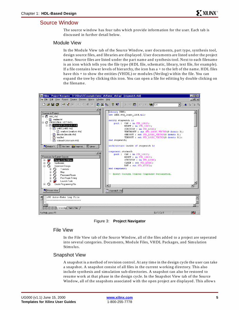
2. From Project Navigator select File->Open Project.
3. In the Directories list, browse to C:\XILINX\iSEexamples\WTUT_VHD or WTUT_VER. Double click on the wtut_vhd.npl or wtut_ver.npl.
Copying the Tutorial Files (Optional)You can either work within the project directory as it has been installed from the CD, or you can make a copy to work on. To make a working copy of the tutorial files use Windows Explorer to copy the WTUT_VER or WTUT_VHD directories to another location. The WTUT_VER and WTUT_VHD project directories contain all of the necessary project files.
Design DescriptionThe design used in this tutorial is a hierarchical, HDL-based design, meaning that the top-level design file is an HDL file that references several other lower-level macros. The lower-level macros are either HDL modules or CORE Generator modules.
The design begins as an unfinished design. Throughout the tutorial, you complete the design by generating some of the modules from scratch and by completing some others from existing files. When the design is complete, you simulate it to verify the design’s functionality.
Figure 1: Foundation Series ISE Project Navigator Icon
Figure 2: Getting Started Dialog Box
UG000 (v1.1) June 15, 2000 www.xilinx.com 3Templates for Xilinx User Guides 1-800-255-7778

Chapter 1: HDL-Based DesignR
Watch is a simple runner ’s stopwatch. There are three external inputs, and three external output buses in the completed design. The system clock is an externally generated signal. The following list summarizes the input lines and output buses.
Inputs:
• STRTSTOP —Starts and stops the stopwatch. This is an active low signal which acts like the start/stop button on a runner ’s stopwatch.
• RESET—Resets the stopwatch to 00.0 after it has been stopped.• CLK—Externally generated system clock
Outputs:
• TENSOUT[6:0]—7-bit bus which represents the Ten’s digit of the stopwatch value. This bus is in 7-segment display format viewable on the 7-segment LED display.
• ONESOUT[6:0]—Similar to TENSOUT bus above, but represents the One’s digit of the stopwatch value.
• TENTHSOUT[9:0]—10-bit bus which represents the Tenths’ digit of the stopwatch value. This bus is one-hot encoded.
The completed design consists of the following functional blocks.
• STATMACH• State Machine module.
• CNT60
HDL-based module which counts from 0 to 59, decimal. This macro has two 4-bit outputs, which represent the ones and tens digits of the decimal values, respectively.
• TENTHS
CORE Generator 4-bit, binary encoded counter. This macro outputs a 4-bit code which is decoded to represent the tenths digit of the watch value as a 10-bit one-hot encoded value.
• HEX2LED
HDL-based macro. This macro decodes the ones and tens digit values from hexadecimal to 7-segment display format.
• SMALLCNTR
A simple Counter.
• Decode
Decoded the CORE Generator output from 4-bit binary to a 10-bit one hot output.
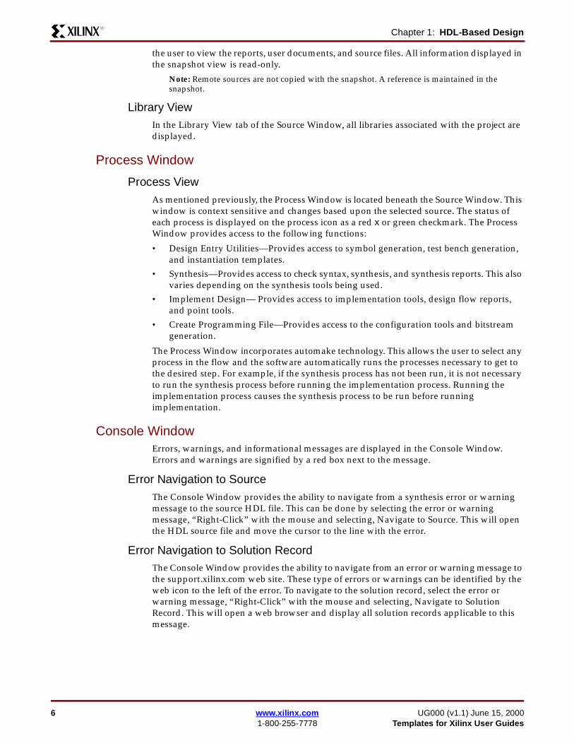
The Project NavigatorThe Project Navigator controls all aspects of the design flow. Through the Project Navigator, you can access all of the various design entry and design implementation tools. You can also access the files and documents associated with your project. The Project Navigator maintains a flat directory structure, therefore the user must maintain revision control through the use of snapshots.
The Project Navigator is divided into four main subwindows. On the top left is the Source Window which hierarchically displays the elements included in the project. Beneath the Source Window is the Process Window which displays available processes. The third window at the bottom of the Project Navigator is the Message Console and shows status messages, errors, and warnings and is updated during all project actions. The fourth window to the right is the HDL Editor. From this window a user edits source files and accesses the Language Templates. These windows are discussed in more detail in the following sections.
4 www.xilinx.com UG000 (v1.1) June 15, 20001-800-255-7778 Templates for Xilinx User Guides
Chapter 1: HDL-Based DesignR
Source WindowThe source window has four tabs which provide information for the user. Each tab is discussed in further detail below.
Module ViewIn the Module View tab of the Source Window, user documents, part type, synthesis tool, design source files, and libraries are displayed. User documents are listed under the project name. Source files are listed under the part name and synthesis tool. Next to each filename is an icon which tells you the file type (HDL file, schematic, library, text file, for example). If a file contains lower levels of hierarchy, the icon has a + to the left of the name. HDL files have this + to show the entities (VHDL) or modules (Verilog) within the file. You can expand the tree by clicking this icon. You can open a file for editting by double clicking on the filename.
File ViewIn the File View tab of the Source Window, all of the files added to a project are seperated into several categories. Documents, Module Files, VHDL Packages, and Simulation Stimulus.
Snapshot ViewA snapshot is a method of revision control. At any time in the design cycle the user can take a snapshot. A snapshot consist of all files in the current working directory. This also include synthesis and simulation sub-directories. A snapshot can also be restored to resume work at that phase in the design cycle. In the Snapshot View tab of the Source Window, all of the snapshots associated with the open project are displayed. This allows
Figure 3: Project Navigator
UG000 (v1.1) June 15, 2000 www.xilinx.com 5Templates for Xilinx User Guides 1-800-255-7778
Chapter 1: HDL-Based DesignR
the user to view the reports, user documents, and source files. All information displayed in the snapshot view is read-only.
Note: Remote sources are not copied with the snapshot. A reference is maintained in the snapshot.
Library ViewIn the Library View tab of the Source Window, all libraries associated with the project are displayed.
Process Window
Process ViewAs mentioned previously, the Process Window is located beneath the Source Window. This window is context sensitive and changes based upon the selected source. The status of each process is displayed on the process icon as a red x or green checkmark. The Process Window provides access to the following functions:
• Design Entry Utilities—Provides access to symbol generation, test bench generation, and instantiation templates.
• Synthesis—Provides access to check syntax, synthesis, and synthesis reports. This also varies depending on the synthesis tools being used.
• Implement Design— Provides access to implementation tools, design flow reports, and point tools.
• Create Programming File—Provides access to the configuration tools and bitstream generation.
The Process Window incorporates automake technology. This allows the user to select any process in the flow and the software automatically runs the processes necessary to get to the desired step. For example, if the synthesis process has not been run, it is not necessary to run the synthesis process before running the implementation process. Running the implementation process causes the synthesis process to be run before running implementation.
Console WindowErrors, warnings, and informational messages are displayed in the Console Window. Errors and warnings are signified by a red box next to the message.
Error Navigation to SourceThe Console Window provides the ability to navigate from a synthesis error or warning message to the source HDL file. This can be done by selecting the error or warning message, “Right-Click” with the mouse and selecting, Navigate to Source. This will open the HDL source file and move the cursor to the line with the error.
Error Navigation to Solution RecordThe Console Window provides the ability to navigate from an error or warning message to the support.xilinx.com web site. These type of errors or warnings can be identified by the web icon to the left of the error. To navigate to the solution record, select the error or warning message, “Right-Click” with the mouse and selecting, Navigate to Solution Record. This will open a web browser and display all solution records applicable to this message.
6 www.xilinx.com UG000 (v1.1) June 15, 20001-800-255-7778 Templates for Xilinx User Guides

Chapter 1: HDL-Based DesignR
UG000 (v1.1) June 15, 2000 www.xilinx.com 7Templates for Xilinx User Guides 1-800-255-7778
Chapter 1: HDL-Based DesignR
SnapshotsSnapshots provide the user the ability to maintain revision control over the design. A snapshot contains all of the files in the project directory.
Creating a SnapshotA snapshot can be created by selecting Project → Take a Snapshot. This opens the Take a Snapshot of the Project dialog box. This allows the user to enter the snapshot name and any comments associated with the snapshot. The snapshot contains all of the files in the project directory along with project settings.
Restoring a SnapshotThe Snapshot View, of the Source Window, contains a list of all the snapshots available in the current project. Since snapshots are read-only, a snapshot must be restored in order to continue work. To do this select the snapshot and select Project→Replace with Snapshot. The user is prompted to create a snapshot of the current project directory and restore the selected snapshot for further work.
Viewing a SnapshotThe Snapshot View, of the Source Window, contains a list of all the snapshots available in the current project. A snapshot can be opened to review report or verify process status by select the snapshot then “Right-Click” and selecting Open.
XST or FPGA Express Synthesis
Xilinx Synthesis Technology (XST)
Supported Devices• Virtex/ -E• Spartan-II
• XC9500™ /XL /XV
Process PropertiesProcess properties allow the user to control the synthesis results of XST. Two commonly used properties are Optimization Goal and Optimization Effort. Through these properties the user can control the synthesis results for area or speed and the amount of time the synthesizer runs.
More detailed information is available in the XST User Guide.
FPGA Express
Supported Devices• Virtex/ -E
• Spartan/XL/-II• XC9500/ XL /XV
• XC4000™ E /EX /XL /XV /XLA
Process PropertiesProcess properties allow the user to control the synthesis results of FPGA Express. Two commonly used properties are Optimization Goal and Optimization Effort. Through these
8 www.xilinx.com UG000 (v1.1) June 15, 20001-800-255-7778 Templates for Xilinx User Guides

Chapter 1: HDL-Based DesignR
properties the user can control the synthesis results for area or speed and the amount of time the synthesizer runs.
More detailed information is available in the FPGA Express online help.
Design EntryIn this hierarchical design, you will examine HDL files, correct syntax errors, create an HDL macro, and add a CORE Generator module. This tutorial gives you experience with creating and using each type of design macro so that you can apply these procedures to your own design.
With wtut_vhd or wtut_ver project open in Project Navigator, Figure 4 is the source window which displays all of source files currently added to the project, with the associated entity or module names. In the current project smallcntr and hex2led are instantiated but the associated entity or module is not defined in the project. Instantiated components with no entity or module declaration are displayed with a red ?.
Adding Source FilesYou must add HDL files to the project before they can be synthesized. Four HDL files have already been added to this project, but have not yet been analyzed. To analyze the source files, select stopwatch.vhd or stopwatch.v in the source window. Upon selecting the HDL file, the process window displays all processes available for this file.
Now add the remaining HDL file to the project. Select Project → Add Source and select smallcntr.vhd or smallcntr.v from the project directory. In the Choose Source Type dialog, select HDL module and click Ok. The red ? for smallcntr should change to a V.
Adding the file to the project does not cause it to be analyzed. To analyze the source files, select stopwatch.vhd or stopwatch.v in the source window. Upon selecting the HDL file, the process window displays all processes available for this file. Select Analyze Hierarchy under Synthesize to update these files.
¼
Figure 4: Source Window
UG000 (v1.1) June 15, 2000 www.xilinx.com 9Templates for Xilinx User Guides 1-800-255-7778
Chapter 1: HDL-Based DesignR
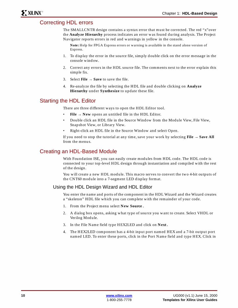
Correcting HDL errorsThe SMALLCNTR design contains a syntax error that must be corrected. The red “x”over the Analyze Hierarchy process indicates an error was found during analysis. The Project Navigator reports errors in red and warnings in yellow in the console.
Note: Help for FPGA Express errors or warning is available in the stand alone version of Express.
1. To display the error in the source file, simply double click on the error message in the console window.
2. Correct any errors in the HDL source file. The comments next to the error explain this simple fix.
3. Select File → Save to save the file.
4. Re-analyze the file by selecting the HDL file and double clicking on Analyze Hierarchy under Synthesize to update these file.
Starting the HDL EditorThere are three different ways to open the HDL Editor tool.
• File → New opens an untitled file in the HDL Editor.
• Double click an HDL file in the Source Window from the Module View, File View, Snapshot View, or Library View.
• Right-click an HDL file in the Source Window and select Open.
If you need to stop the tutorial at any time, save your work by selecting File → Save All from the menus.
Creating an HDL-Based ModuleWith Foundation ISE, you can easily create modules from HDL code. The HDL code is connected to your top-level HDL design through instantiation and compiled with the rest of the design.
You will create a new HDL module. This macro serves to convert the two 4-bit outputs of the CNT60 module into a 7-segment LED display format.
Using the HDL Design Wizard and HDL EditorYou enter the name and ports of the component in the HDL Wizard and the Wizard creates a “skeleton” HDL file which you can complete with the remainder of your code.
1. From the Project menu select New Source.
2. A dialog box opens, asking what type of source you want to create. Select VHDL or Verilog Module.
3. In the File Name field type HEX2LED and click on Next.
4. The HEX2LED component has a 4-bit input port named HEX and a 7-bit output port named LED. To enter these ports, click in the Port Name field and type HEX. Click in
10 www.xilinx.com UG000 (v1.1) June 15, 20001-800-255-7778 Templates for Xilinx User Guides

Chapter 1: HDL-Based DesignR
the Direction field and set the direction to in. In the MSB field enter 3, and the LSB field enter 0.
5. Repeat the previous step for the LED[6:0] output bus. Be sure that the direction is set to Out.
6. Click Next to complete the Wizard session. A description of the module is now displayed. Click on Finish to open the “skeleton” HDL file in the HDL Editor.†
Figure 5: HDL Wizard
Figure 6: Skeleton VHDL File
UG000 (v1.1) June 15, 2000 www.xilinx.com 11Templates for Xilinx User Guides 1-800-255-7778

Chapter 1: HDL-Based DesignR
In the HDL Editor, the ports are already declared in the HDL file, and some of the basic file structure is already in place. Keywords are printed in blue, data types in red, comments in green, and values are black. This color-coding enhances readability and recognition of typographical errors.
Using the Language TemplatesYou use the templates in the Language Templates for commonly used HDL constructs, as well as synthesis templates for commonly used logic components such as counters, D flip-flops, multiplexers, and primitives. You can add your own templates to the Language Template for components or constructs you use often.
1. To invoke the Language Assistant, select Edit→ Language Templates.
2. Each HDL language in the Language Template is divided into four sections: Component Instantiations, Language Templates, Synthesis Templates, and User Templates. To expand the view of any of these sections, click the + next to the topic. Click any of the listed templates to view the template in the right hand pane.
3. Use the template called HEX2LED Converter located under the Synthesis Templates heading for VHDL or Verilog. Use the appropriate template for the language you are using. Locate this template and preview it in the right hand pane by clicking the
Figure 7: Skeleton Verilog File
12 www.xilinx.com UG000 (v1.1) June 15, 20001-800-255-7778 Templates for Xilinx User Guides
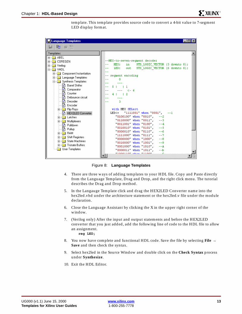
Chapter 1: HDL-Based DesignR
template. This template provides source code to convert a 4-bit value to 7-segment LED display format.
4. There are three ways of adding templates to your HDL file. Copy and Paste directly from the Language Template, Drag and Drop, and the right click menu. The tutorial describes the Drag and Drop method.
5. In the Langauge Template click and drag the HEX2LED Converter name into the hex2led.vhd under the architecture statement or the hex2led.v file under the module declaration.
6. Close the Language Assistant by clicking the X in the upper right corner of the window.
7. (Verilog only) After the input and output statements and before the HEX2LED converter that you just added, add the following line of code to the HDL file to allow an assignment.
reg LED;
8. You now have complete and functional HDL code. Save the file by selecting File → Save and then check the syntax.
9. Select hex2led in the Source Window and double click on the Check Syntax process under Synthesize.
10. Exit the HDL Editor.
Figure 8: Language Templates
UG000 (v1.1) June 15, 2000 www.xilinx.com 13Templates for Xilinx User Guides 1-800-255-7778

Chapter 1: HDL-Based DesignR
Creating a CoreGEN ModuleCORE Generator is a graphical interactive design tool you use to create high-level modules such as counters, shift registers, RAM and multiplexers. You can customize and pre-optimize the modules to take advantage of the inherent architectural features of the Xilinx FPGA architectures, such as Fast Carry Logic for arithmetic functions, and on-chip RAM for dual-port and synchronous RAM.
In this section, you create a CORE Generator module called Tenths. Tenths is a 4-bit binary encoded counter. The 4-bit number is decoded to count the tenths digit of the stopwatch’s time value.
Creating the Core Generator moduleYou select the type of module you want in the CORE dialog box as well as the specific features of the module. You can invoke this GUI from the Project Navigator New Source Wizard.
1. In Project Navigator select Project→ New Source.
2. Select Coregen IP, enter tenths in the File Name field and click Next and then Finish.
3. The Xilinx CORE Generator 3.1i opens and displays a list of possible COREs available. Double Click on Basic Elements - Counters.
4. Double Click on Binary Counter to open the Binary Counter dialog. This dialog allows the user to customize the counter to the design specifications.
5. Fill in the Binary Counter dialog with the following settings.
- Component Name: tenthsDefines the name of the module.
- Output Width: 4Defines the width of the output bus.
- Operation: UpDefines how the counter will operate. This field is dependant on the type of module you select.
- Count Restrictions: Restrict Count to A.
- This dictates the maximum count value.- Output Options: Threshold0 set to A.
- Signal goes high when the value specified has been reached.- Output Options: Registered
6. Click on the Register Options button to open the Register Options dialog. Enter the following settings.
- Clock Enable: Selected- Asynchronous Settings: Init with a value of 1.
- Synchronous Settings: None.- Click Ok.
7. Check that only the following pins are used.
- AINIT- CE
- Q- Q_Thresh0
- CLK
14 www.xilinx.com UG000 (v1.1) June 15, 20001-800-255-7778 Templates for Xilinx User Guides

Chapter 1: HDL-Based DesignR
8. Click Generate. The module is created and automatically added to the project library.
A number of files are added to the project directory. These files are:
• TENTHS.EDNThis file is the netlist that is used during the Translate phase of implementation.
• TENTHS.VHO or TENTHS.VEOThis is the instantiation template that is used to incorporate the CORE Generator module in your source HDL.
• TENTHS.XCOThis file stores the configuration information for the Tenths module.
• COREGEN.PRJThis file stores the Coregen configuration for the project.
9. Select Cancel and close Core Generator.
Instantiating the Coregen Module in the HDL Code
VHDL Flow
1. Open STOPWATCH.VHD in the HDL Editor.
2. Place your cursor after the line that states:“-- Insert Coregen Counter Component Declaration”
Select Edit → Insert File and choose Tenths.vho. The VHDL template file for the Coregen instantiation is inserted.
The Component Declaration does not need to be modified.
Figure 9: CoreGen Module Selector
UG000 (v1.1) June 15, 2000 www.xilinx.com 15Templates for Xilinx User Guides 1-800-255-7778
Chapter 1: HDL-Based DesignR
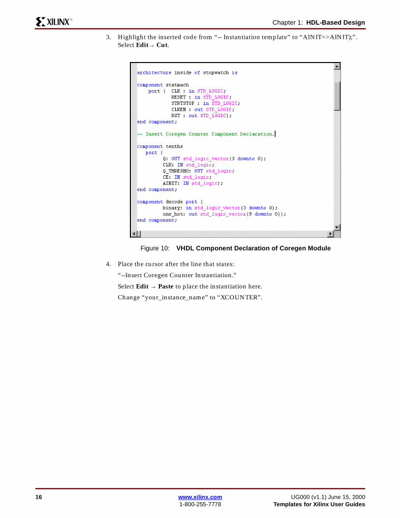
3. Highlight the inserted code from “-- Instantiation template” to “AINIT=>AINIT);”. Select Edit→ Cut.
4. Place the cursor after the line that states:
“--Insert Coregen Counter Instantiation.”
Select Edit → Paste to place the instantiation here.
Change “your_instance_name” to “XCOUNTER”.
Figure 10: VHDL Component Declaration of Coregen Module
16 www.xilinx.com UG000 (v1.1) June 15, 20001-800-255-7778 Templates for Xilinx User Guides
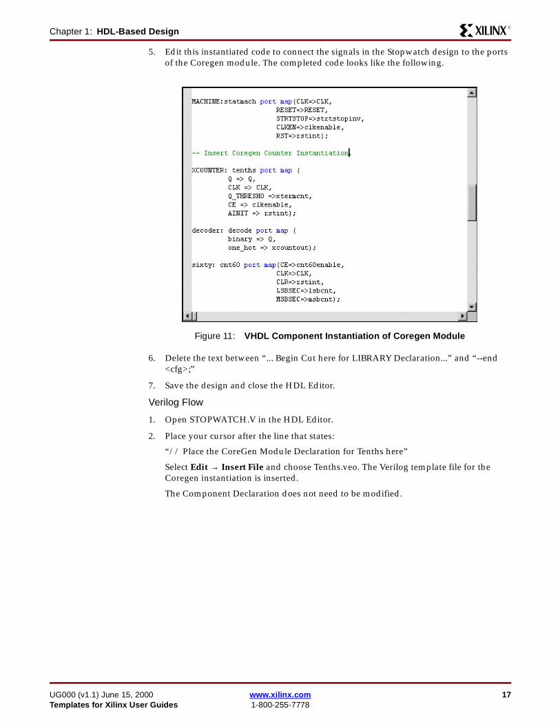
Chapter 1: HDL-Based DesignR
5. Edit this instantiated code to connect the signals in the Stopwatch design to the ports of the Coregen module. The completed code looks like the following.
6. Delete the text between “... Begin Cut here for LIBRARY Declaration...” and “--end <cfg>;”
7. Save the design and close the HDL Editor.
Verilog Flow
1. Open STOPWATCH.V in the HDL Editor.
2. Place your cursor after the line that states:
“// Place the CoreGen Module Declaration for Tenths here”
Select Edit → Insert File and choose Tenths.veo. The Verilog template file for the Coregen instantiation is inserted.
The Component Declaration does not need to be modified.
Figure 11: VHDL Component Instantiation of Coregen Module
UG000 (v1.1) June 15, 2000 www.xilinx.com 17Templates for Xilinx User Guides 1-800-255-7778

Chapter 1: HDL-Based DesignR
3. Highlight the inserted code from “Tenths YourInstanceName” to “.AINIT=(AINIT));”. Select Edit → Cut.
4. Place the cursor after the line that states:
“// Place the CoreGen Component Instantiation for Tenths here.”
Select Edit → Paste to place the instantiation here.
Change “YourInstanceName” to “XCOUNTER”.
Figure 12: Verilog Module Declaration of Coregen Module
18 www.xilinx.com UG000 (v1.1) June 15, 20001-800-255-7778 Templates for Xilinx User Guides
Chapter 1: HDL-Based DesignR
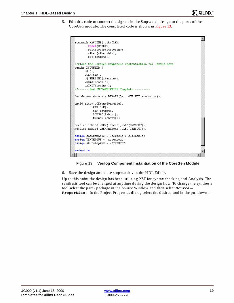
5. Edit this code to connect the signals in the Stopwatch design to the ports of the CoreGen module. The completed code is shown in Figure 13.
6. Save the design and close stopwatch.v in the HDL Editor.
Up to this point the design has been utilizing XST for syntax checking and Analysis. The synthesis tool can be changed at anytime during the design flow. To change the synthesis tool select the part - package in the Source Window and then select Source→ Properties. In the Project Properties dialog select the desired tool in the pulldown in
Figure 13: Verilog Component Instantiation of the CoreGen Module
UG000 (v1.1) June 15, 2000 www.xilinx.com 19Templates for Xilinx User Guides 1-800-255-7778

Chapter 1: HDL-Based DesignR
the Synthesis Tool column. Once this selection has been made proceed to the appropriate Synthesis section.
Synthesizing the Design with XSTNow that the design has been entered and analyzed, the next step is to synthesize the design. In this step, the HDL files are translated into gates and optimized to the target architecture.
1. Select STOPWATCH.VHD (or STOPWATCH.V) and double click on the Synthesize process in the Process Window.
This step can also be done by selecting STOPWATCH.VHD (or STOPWATCH.V), and then selecting the Synthesize process in the Process Window. Now select Process→ Run.
2. At this point, an EDN file exists for the Stopwatch design. See “” chapter to perform a pre-synthesis simulation of this design, refer to “” chapter to place and route the design, or refer to the“” chapter for post place and route simulation.Note: For more information concerning XST constraints, options, reports, or running XST via command line see the XST User Guide at http://support.xilinx.com.
Figure 14: Specifying Synthesis Tool
Figure 15: Synthesis/Implementation Window
20 www.xilinx.com UG000 (v1.1) June 15, 20001-800-255-7778 Templates for Xilinx User Guides
Chapter 1: HDL-Based DesignR
Synthesizing the Design with FPGA ExpressSynthesizing the Design with FPGA Express.
Now that the design has been entered and analyzed, the next step is to synthesize the design. In this step, the HDL files are translated into gates and optimized to the target architecture.
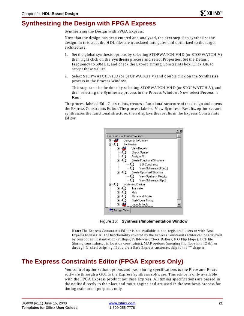
1. Set the global synthesis options by selecting STOPWATCH.VHD (or STOPWATCH.V) then right click on the Synthesis process and select Properties. Set the Default Frequency to 50MHz, and check the Export Timing Constraints box. Click OK to accept these values.
2. Select STOPWATCH.VHD (or STOPWATCH.V) and double click on the Synthesize process in the Process Window.
This step can also be done by selecting STOPWATCH.VHD (or STOPWATCH.V), and then selecting the Synthesize process in the Process Window. Now select Process → Run.
The process labeled Edit Constraints, creates a functional structure of the design and opens the Express Constraints Editor. The process labeled View Synthesis Results, optimizes and synthesizes the functional structure, then displays the results in the Express Constraints Editor.
Note: The Express Constraints Editor is not available to non-registered users or with Base Express licenses. All the functionality covered by the Express Constraints Editor can be achieved by component instantiation (Pullups, Pulldowns, Clock Buffers, I/O Flip Flops), UCF file (timing constraints, pin location constraints), MAP options (merging flip flops into IOBs), or through fe_shell scripting. If you are a Base Express customer, skip to the “” chapter.
The Express Constraints Editor (FPGA Express Only)You control optimization options and pass timing specifications to the Place and Route software through a GUI in the Express Synthesis software. This editor is only available with the FPGA Express product not Base Express. All timing specifications are passed in the netlist directly to the place and route engine and are used in the synthesis process for timing estimation purposes only.
Figure 16: Synthesis/Implementation Window
UG000 (v1.1) June 15, 2000 www.xilinx.com 21Templates for Xilinx User Guides 1-800-255-7778
Chapter 1: HDL-Based DesignR
• Clocks
The Default Frequency set in Synthesize Process Properties, and is applied to all clocks in the design. To change the specification of a clock, click inside the box to the right of the clock and select Define. Enter the clock period or give the rise and fall times.
• Paths
All types of paths that can be covered by timing specifications are listed here, with unique specifications given for each clock in the design. To modify these specifications, enter a new delay in the Req. Delay column.
To create a subpath within a path, right click the source(from) or destination(to) and select New Subpath. Give the subpath a new name and delay value, then select sources and destinations by double clicking the instances. You can also use wildcards in the selection filters to choose a group of elements.
• Ports
With the Ports tab, you set input and out delay requirements, assign clock buffers, insert pullup or pulldown resistors in the I/O, set delay properties for input registers, set slew rate, disable the use of I/O registers, and assign pin locations. For all but the pin locations, click in the box to use the pulldown menu. For pin locations, type the pin number in the box.
• Modules
With the Modules tab, you can keep or eliminate hierarchy and disable resource sharing. You can also override the default settings for effort and area versus speed at the module level. Block level Incremental Synthesis is also enabled here.
• Xilinx Options
The Ignore unlinked cells during GSR mapping option directs Express to infer a global reset signal (and, therefore, insert the STARTUP module), even if black boxes have been instantiated. Express cannot know the reset characteristics of any logic in black boxes, so it will not insert STARTUP unless you check this option.
Using the Express Constraints Editor (FPGA Express Only)Xilinx recommends that you let the automatic placement and routing program, PAR, define the pinout of your design. Pre-assigning locations to the pins can sometimes degrade the performance of the place-and-route tools. However, it is usually necessary, at some point, to lock the pinout of a design so that it can be integrated into a PCB (printed circuit board).
Define the initial pinout by running the place-and-route tools without pin assignments, then locking down the pin placement so that it reflects the locations chosen by the tools. Assign locations to the pins in the Watch design so that the design can function in a Xilinx demonstration board. Because the design is simple and timing is not critical, these pin assignments do not adversely affect the ability of PAR to place-and-route the design.
For HDL-based designs, these pin assignments can be done in a User Constraints File (.UCF) or with the Express Constraints Editor. Although UCF files are provided for this tutorial, you will assign the pin location constraints in the Express Constraints Editor.
1. In the Express Constraint Editor, click the Import Constraints button. Select WATCHVHD.EXC or WATCHVER.EXC, depending on the language you are using. These files are located in the project directory.
This file has been created for you. The only difference you should see between your initial constraints and the ones saved in the .EXC file is the set of pin locations under the Ports tab.
22 www.xilinx.com UG000 (v1.1) June 15, 20001-800-255-7778 Templates for Xilinx User Guides
Chapter 1: HDL-Based DesignR
You can save Constraint Editor settings for a design by selecting File → Export Constraints. When this .EXC file is read in for a later synthesis run, all constraints are re-established in the GUI, as long as they can be matched to instances in the current version.
2. Under the Paths tab, click in the box in Row 2 below the Req. Delay header (from All Input Ports to RC-CLK). Change the delay to 15. Under the Ports tab, the Input Delays for RESET and STRTSTOP have changed to 15, as these represent all the Pad to Setup delays.
You can change the values of individual Input or Output Delays by clicking the value in the Ports tab and either editing the value there or using the pulldown tab to select a value or define a new one. Change the values on one of the output signals using one of these methods.
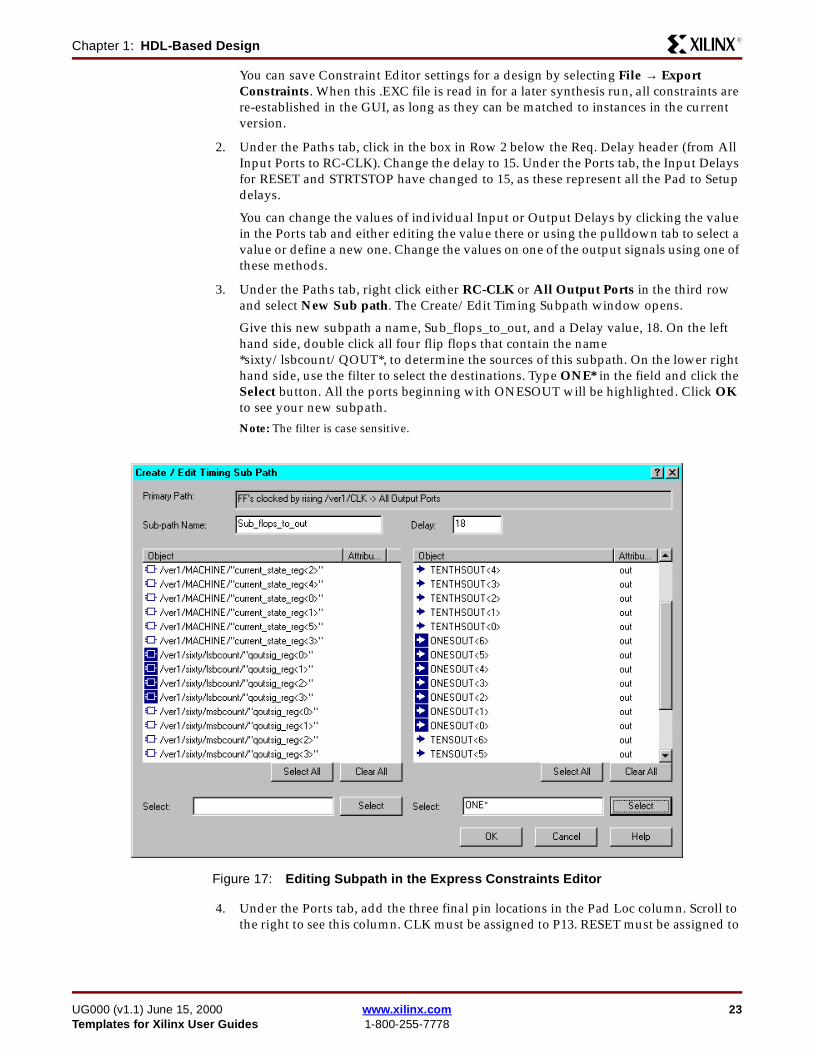
3. Under the Paths tab, right click either RC-CLK or All Output Ports in the third row and select New Sub path. The Create/Edit Timing Subpath window opens.
Give this new subpath a name, Sub_flops_to_out, and a Delay value, 18. On the left hand side, double click all four flip flops that contain the name *sixty/lsbcount/QOUT*, to determine the sources of this subpath. On the lower right hand side, use the filter to select the destinations. Type ONE* in the field and click the Select button. All the ports beginning with ONESOUT will be highlighted. Click OK to see your new subpath.
Note: The filter is case sensitive.
4. Under the Ports tab, add the three final pin locations in the Pad Loc column. Scroll to the right to see this column. CLK must be assigned to P13. RESET must be assigned to
Figure 17: Editing Subpath in the Express Constraints Editor
UG000 (v1.1) June 15, 2000 www.xilinx.com 23Templates for Xilinx User Guides 1-800-255-7778
Chapter 1: HDL-Based DesignR
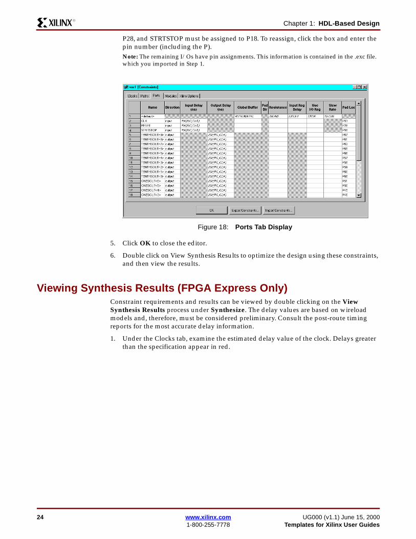
P28, and STRTSTOP must be assigned to P18. To reassign, click the box and enter the pin number (including the P).Note: The remaining I/Os have pin assignments. This information is contained in the .exc file. which you imported in Step 1.
5. Click OK to close the editor.
6. Double click on View Synthesis Results to optimize the design using these constraints, and then view the results.
Viewing Synthesis Results (FPGA Express Only)Constraint requirements and results can be viewed by double clicking on the View Synthesis Results process under Synthesize. The delay values are based on wireload models and, therefore, must be considered preliminary. Consult the post-route timing reports for the most accurate delay information.
1. Under the Clocks tab, examine the estimated delay value of the clock. Delays greater than the specification appear in red.
Figure 18: Ports Tab Display
24 www.xilinx.com UG000 (v1.1) June 15, 20001-800-255-7778 Templates for Xilinx User Guides

Chapter 1: HDL-Based DesignR
2. Under the Paths tab, examine the estimated delays for the paths and subpath. Click the source or destination of a path to see the members of the path, and click a specific path to see the individual segments of that path.
3. Examine the Ports tab to see that all of the settings and delays have been assigned and met.
4. Under the Modules tab, you can examine the elements used to synthesize this design. Click the box in the second row under Area and select Details. This section summarizes all the design elements used in the Stopwatch design that Express knows about.
Since the Tenths module is a CoreGEN component and has not been synthesized by Express, it is UNLINKED and no summary information is available.
Note: Black boxes (modules not read into the Express design environment) are always noted as UNLINKED in the Express reports. As long as the underlying netlist (.xnf, .ngo, .ngc or .edn) for a black box exists in the project directory, the Implementation tools merge the netlist in during the Translate phase. Since the Tenths module was built using Coregen called from the project, the tenths EDN file will be found.
5. Click OK to close the editor.
At this point, an EDN file exists for the Stopwatch design. See “” chapter to perform a pre-synthesis simulation of this design,refer to the“” chapter to place and route the design, or refer to the“” chapter for post place and route simulation.
Figure 19: Estimated Timing Data Under Paths Tab
UG000 (v1.1) June 15, 2000 www.xilinx.com 25Templates for Xilinx User Guides 1-800-255-7778

Chapter 1: HDL-Based DesignR
26 www.xilinx.com UG000 (v1.1) June 15, 20001-800-255-7778 Templates for Xilinx User Guides
R
Chapter 2
Schematic-Based Design
This chapter guides you through a typical FPGA schematic-based design procedure using a design of a runner ’s stopwatch called “Watch”. The design example used in this tutorial demonstrates many device features, software features, and design flow practices that you can apply to your own design. The Watch design targets a Virtex device; however, all of the principles and flows taught are applicable to any Xilinx device family, unless otherwise noted.
For an example of how to design with CPLDs, see the online help by selecting Help → Foundation ISE Help Contents from the Project Navigator. Under Tutorials, select CPLD Design Flows.
In the first part of the tutorial, you will use the Foundation ISE design entry tools to complete the design. The design is composed of schematic elements, a state machine, a CORE Generator component, and an HDL macro. After the design is successfully entered in the Schematic Editor, it is ready for functional simulation with the Modelsim simulator, implementation with the Xilinx Implementation Tools, and timing simulation.
This chapter includes the following sections.
• “Getting Started”
• “Design Description”• “The Project Navigator”
• “XST or FPGA Express Synthesis”• “Design Entry”
Getting StartedThe following subsections describe the basic requirements for running the tutorial.
NomenclatureIn this tutorial, the following terms are used:
• “Virtex family” includes the Virtex, Spartan-II and Virtex-E devices only.
• “Right-click” means click the right mouse button. Unless specified, all other mouse operations are performed with the left mouse button.
Throughout this tutorial, file names, project names, and directory names (paths) are specified in lower case. The design is referred to as Watch.
Required SoftwareThe Xilinx Foundation Series ISE package, Version 3.1i, is required to perform this tutorial. The design requires that you have installed the Virtex libraries and device files and are
UG000 (v1.1) June 15, 2000 www.xilinx.com 27Templates for Xilinx User Guides 1-800-255-7778
Chapter 2: Schematic-Based DesignR
licensed for FPGA Express or Base Express. You must also have the Watch projects which may be downloaded from http://support.xilinx.com.
Note: A Foundation Express license is required to access the Express Constraints GUI.
Installing the TutorialThis tutorial assumes that the software is installed in the default location C:\XILINX. If you have installed the software in a different location, substitute your installation path for C:\XILINX\wtut_sc.
Unzip the tutorial projects in the C:\XILINX directory and replace any existing files. The files downloaded from the web have been updated.
Note: For detailed instructions, refer to the Foundation Series ISE 3.1i Install and Release Document.
Tutorial Project Directories and FilesThe following schematic project directories can be downloaded and installed with the tutorial.
• c:\XILINX\iSEexamples\wtut_sc (incomplete schematic tutorial)
• c:\XILINX\iSEexamples\watch_sc(complete schematic tutorial)
The schematic tutorial files are copied into these directories.
The wtut_sc project contains an incomplete copy of the tutorial design. You will create the remaining files when you perform the tutorial. As described in a later step, you can copy this project to another area and perform the tutorial in this new area if desired.
The watch_sc solution project contains the design files for the completed tutorial, including schematics and the bitstream file.To conserve disk space, some intermediate files are not provided. Do not overwrite any files in the solutions directories.
Starting the Project Navigator1. Double click the Foundation Series ISE Project Navigator icon on your desktop or
select Programs → Xilinx Foundation Series ISE 3.1i→ Project Navigator from the Start menu.
Figure 20: Foundation Series ISE Project Navigator Icon
28 www.xilinx.com UG000 (v1.1) June 15, 20001-800-255-7778 Templates for Xilinx User Guides

Chapter 2: Schematic-Based DesignR
2. From Project Navigator select File->Open Project.
3. In the Directories list, browse to C:\XILINX\iSEexamples\WTUT_SC. Double click on the wtut_sc.npl.
Copying the Tutorial Files (Optional)You can either work within the project directory as it has been downloaded, or you can make a copy to work on. To make a working copy of the tutorial files use Windows Explorer to copy the WTUT_SC directory to another location. The WTUT_SC project directory contains all of the necessary project files.
Design DescriptionThroughout this tutorial, the design is referred to as Watch.
The design used in this tutorial is a hierarchical, schematic-based design, meaning that the top-level design file is a schematic sheet which refers to several other lower-level macros. The lower-level macros are a variety of different types of modules including schematic-based modules, CoreGEN modules, state machine modules, and HDL modules.
The design begins as an unfinished design. Throughout the tutorial, you will complete the design by creating some of the modules, and by completing some others from existing files. After the design is complete, you will simulate it to verify the functionality.
Figure 21: Getting Started Dialog Box
UG000 (v1.1) June 15, 2000 www.xilinx.com 29Templates for Xilinx User Guides 1-800-255-7778

Chapter 2: Schematic-Based DesignR
Watch is a simple runner’s stopwatch. The completed schematic is shown in the following figure.
There are three external inputs and three external outputs in the completed design. The following list summarizes the inputs and outputs and their functions.
Inputs:
• CLK—System clock for the Watch design.
• STRTSTOP—Starts and stops the stopwatch. This is an active-low signal which acts like the start/stop button on a runner ’s stopwatch.
• RESET—Resets the stopwatch to 00.0 after it has been stopped.
Outputs:
• TENSOUT[6:0]—7-bit bus which represents the Tens digit of the stopwatch value. This bus is in 7-segment display format to be viewable on the 7-segment LED display.
• ONESOUT[6:0]—similar to TENSOUT bus above, but represents the Ones digit of the stopwatch value.
• TENTHSOUT[9:0]—10-bit bus which represents the Tenths digit of the stopwatch value. This bus is one-hot encoded.
The completed design consists of the following functional blocks. Most of these blocks do not appear yet on the schematic sheet in the tutorial project since they will be created during this tutorial.
Figure 22: Completed Watch Schematic
30 www.xilinx.com UG000 (v1.1) June 15, 20001-800-255-7778 Templates for Xilinx User Guides
Chapter 2: Schematic-Based DesignR
Functional Blocks
• STMACH_V
State Machine macro. This module uses Visual Software Solutions StateCAD to enter and implement the state machine.
• CNT60
Schematic-based module which counts from 0 to 59, decimal. This macro has two 4-bit outputs, which represent the ‘ones’ and ‘tens’ digits of the decimal values, respectively.
• TENTHS
CoreGEN 4-bit, binary encoded counter. This macro outputs a 4-bit code which is decoded to represent the tenths digit of the watch value as a 10-bit one-hot encoded value.
• HEX2LED
HDL-based macro. This macro decodes the ones and tens digit values from hexadecimal to 7-segment display format.
• OUTS3
Schematic based macro containing inverters.
• Decode
Decoded the CORE Generator output from 4-bit binary to a 10-bit one hot output.
The Project NavigatorThe Project Navigator controls all aspects of the design flow. Through the Project Navigator, you can access all of the various design entry and design implementation tools. You can also access the files and documents associated with your project. The Project Navigator maintains a flat directory structure, therefore the user must maintain revision control through the use of snapshots.
The Project Navigator is divided into four main subwindows. On the top left is the Source Window which hierarchically displays the elements included in the project. Beneath the Source Window is the Process Window which displays available processes. The third window at the bottom of the Project Navigator is the Message Console and shows status messages, errors, and warnings and is updated during all project actions. The fourth window to the right is the HDL Editor. From this window a user edits source files and accesses the Language Templates. These windows are discussed in more detail in the following sections.
Source WindowThe source window has four tabs which provide information for the user. Each tab is discussed in further detail below.
Module ViewIn the Module View tab of the Source Window, user documents, part type, synthesis tool, design source files, and libraries are displayed. User documents are listed under the project name. Source files are listed under the part name and synthesis tool. Next to each filename is an icon which tells you the file type (HDL file, schematic, library, text file, for example). If a file contains lower levels of hierarchy, the icon has a + to the left of the name. HDL files have this + to show the entities (VHDL) or modules (Verilog) within the file. You can
UG000 (v1.1) June 15, 2000 www.xilinx.com 31Templates for Xilinx User Guides 1-800-255-7778

Chapter 2: Schematic-Based DesignR
expand the tree by clicking this icon. You can open a file for editting by double clicking on the filename.
File ViewIn the File View tab of the Source Window, all of the files added to a project are seperated into several categories. Documents, Module Files, VHDL Packages, and Simulation Stimulus.
Snapshot ViewA snapshot is a method of revision control. At any time in the design cycle the user can take a snapshot. A snapshot consist of all files in the current working directory. This also include synthesis and simulation sub-directories. A snapshot can also be restored to resume work at that phase in the design cycle. In the Snapshot View tab of the Source Window, all of the snapshots associated with the open project are displayed. This allows the user to view the reports, user documents, and source files. All information displayed in the snapshot view is read-only.
Note: Remote sources are not copied with the snapshot. A reference is maintained in the snapshot.
Library ViewIn the Library View tab of the Source Window, all libraries associated with the project are displayed.
Figure 23: Project Navigator
32 www.xilinx.com UG000 (v1.1) June 15, 20001-800-255-7778 Templates for Xilinx User Guides

Chapter 2: Schematic-Based DesignR
Process Window
Process ViewAs mentioned previously, the Process Window is located underneath the Source Window. This window is context sensitive and changes based upon the selected source. The status of each process is displayed on the process icon as a red x or green checkmark. The Process Window provides access to the following functions:
• Design Entry Utilities—Provides access to symbol generation, test bench generation, and instantiation templates.
• Synthesis—Provides access to check syntax, synthesis, and synthesis reports. This also varies depending on the synthesis tools being used.
• Implement Design— Provides access to implementation tools, design flow reports, and point tools.
• Create Programming File—Provides access to the configuration tools and bitstream generation.
The Process Window incorporates automake technology. This allows the user to select any process in the flow and the software automatically runs the processes necessary to get to the desired step. For example, if the synthesis process has not been run, it is not necessary to run the synthesis process before running the implementation process. Running the implementation process causes the synthesis process to be run before running implementation.
Console WindowErrors, warnings, and informational messages are displayed in the Console Window. Errors and warnings are signified by a red box next to the message.
Error Navigation to SourceThe Console Window provides the ability to navigate from a synthesis error or warning message to the source HDL file. This can be done by selecting the error or warning message, “Right-Click” with the mouse and selecting, Navigate to Source. This will open the HDL source file and move the cursor to the line with the error.
Error Navigation to Solution RecordThe Console Window provides the ability to navigate from an error or warning message to the support.xilinx.com web site. These type of errors or warnings can be identified by the web icon to the left of the error. To navigate to the solution record, select the error or warning message, “Right-Click” with the mouse and selecting, Navigate to Solution Record. This will open a web browser and display any solution records applicable to this message.
SnapshotsSnapshots provide the user the ability to maintain revision control over the design. A snapshot contains all of the files in the project directory.
Creating a SnapshotA snapshot can be created by selecting Project → Take a Snapshot. This opens the Take a Snapshot of the Project dialog box. This allows the user to enter the snapshot name and any comments associated with the snapshot. The snapshot contains all of the files in the project directory along with project settings.
UG000 (v1.1) June 15, 2000 www.xilinx.com 33Templates for Xilinx User Guides 1-800-255-7778

Chapter 2: Schematic-Based DesignR
Restoring a SnapshotThe Snapshot View, of the Source Window, contains a list of all the snapshots available in the current project. Since snapshots are read-only, a snapshot must be restored in order to continue work. To do this select the snapshot and select Project→Replace with Snapshot. The user is prompted to create a snapshot of the current project directory and restore the selected snapshot for further work.
Viewing a SnapshotThe Snapshot View, of the Source Window, contains a list of all the snapshots available in the current project. A snapshot can be opened to review report or verify process status by selecting the snapshot then “Right-Click” and selecting Open.
XST or FPGA Express Synthesis
Xilinx Synthesis Technology (XST)
Supported Devices• Virtex/ -E• Spartan-II
• XC9500/XL /XV
Process PropertiesProcess properties allow the user to control the synthesis results of XST. Two commonly used properties are Optimization Goal and Optimization Effort. Through these properties the user can control the synthesis results for area or speed and the amount of time the synthesizer runs.
More detailed information is available in the XST User Guide.
FPGA Express
Supported Devices• Virtex/-E
• Spartan/XL/-II• XC9500/XL /XV
• XC4000E /EX /XL /XV /XLA
Process PropertiesProcess properties allow the user to control the synthesis results of FPGA Express. Two commonly used properties are Optimization Goal and Optimization Effort. Through these properties the user can control the synthesis results for area or speed and the amount of time the synthesizer runs.
More detailed information is available in the FPGA Express online help.
Design EntryIn this hierarchical design, you will create various types of macros, including schematic-based macros, HDL-based macros, state machine macros, and CoreGEN macros. You will learn the process for creating each of these types of macros, and then you will connect them all together to create the completed Watch design. This tutorial gives you experience with
34 www.xilinx.com UG000 (v1.1) June 15, 20001-800-255-7778 Templates for Xilinx User Guides

Chapter 2: Schematic-Based DesignR
creating and using each type of design macro so that you can apply this knowledge to your own design.
Starting the Schematic EditorThere are two different ways to open the Schematic Capture tool.
• From the Project → New Source menu pick. This will open the New Source dialog where the schematic source type can be selected. This will create a new schematic.
• Double click the file name STOPWATCH.SCH in the Source Window.
The Schematic Editor opens with the Watch schematic sheet loaded. The Watch schematic is incomplete at this point. Throughout the tutorial, you create the components to complete the design. The unfinished design is shown in the figure below.
If you need to stop the tutorial at any time, save your work by selecting File → Save from the pulldown menus.
Executing CommandsThere are three ways to execute commands within the Foundation ISE tools: pulldown menus, hotkeys, and toolbar buttons. In most cases, this tutorial instructs you to use the pulldown menus.
HotkeysYou can use the keyboard to execute various commands. These “hotkeys” are listed next to the commands within the pulldown menus. Some of the hotkeys are the function keys, some are single letters, and some require the Ctrl or Alt keys. You cannot customize them.
Figure 24: Incomplete Watch Schematic
UG000 (v1.1) June 15, 2000 www.xilinx.com 35Templates for Xilinx User Guides 1-800-255-7778

Chapter 2: Schematic-Based DesignR
Toolbar ButtonsThere are also toolbars that are located beneath the pulldown menus and to the left of the main Schematic Editor window. Hold your mouse over the buttons to see their function.
Manipulating the ScreenUnder the View pulldown menu is a series of commands that modify the viewing area of the Schematic Editor window.”Zoom In” to comfortably view the schematic.
Creating a Schematic-Based MacroA schematic-based macro consists of a symbol and an underlying schematic. You can create either the underlying schematic or the symbol first, and the tools can automatically generate the corresponding symbol or schematic file, respectively. In the following steps, you create a schematic-based macro by using the New Source Wizard. A template schematic file is then created by the tools, and you complete the schematic with the appropriate logic. The created macro is then automatically added to the project’s library.
The macro you will create is called CNT60. CNT60 is a binary counter with two 4-bit outputs, which represent the Ones and Tens values of the stopwatch. The counter counts from 0 to 59, decimal.
1. Select Project→ New Source from the Project Navigator. The New Source dialog opens.
The New Source dialog provides a list of all available source types. Select Schematic and cnt60 as the file name.
2. Click Next, then Finish.
Figure 25: Schematic Editor
36 www.xilinx.com UG000 (v1.1) June 15, 20001-800-255-7778 Templates for Xilinx User Guides

Chapter 2: Schematic-Based DesignR
This creates a new schematic named cnt60 and adds the schematic to the project.
Creating the CNT60 SchematicYou have now created an empty schematic for the cnt60. The next step is to add the components which comprise the cnt60 macro. You can then reference this macro symbol by placing it on a schematic sheet.
Connectivity—I/O MarkersI/O markers logically connect the CNT60 symbol and its underlying schematic. The name of each pin on the symbol must have a corresponding connector in the underlying schematic.
To add hierarchy connectors manually, you can use the I/O Marker icon on the Drawing Toolbar.
Note: The Drawing Toolbar is displayed by selecting View→ Drawing Toolbar.
When you save a macro, the Schematic Editor checks the I/O markers against the corresponding symbol. If there is a discrepancy, you can let the software update the symbol automatically, or you can modify the symbol manually. I/O markers should be used to connect signals between levels of hierarchy and also to specify the ports on top-level schematic sheets.
Project LibrariesFoundation ISE contains several different types of libraries.
• Schematic: Xilinx Unified Symbol libraries which contain macros and primitives. Engineering Capture System(ECS) contains access to these library elements using the
Figure 26: New Source Dialog
Figure 27: I/O Marker Icon
UG000 (v1.1) June 15, 2000 www.xilinx.com 37Templates for Xilinx User Guides 1-800-255-7778
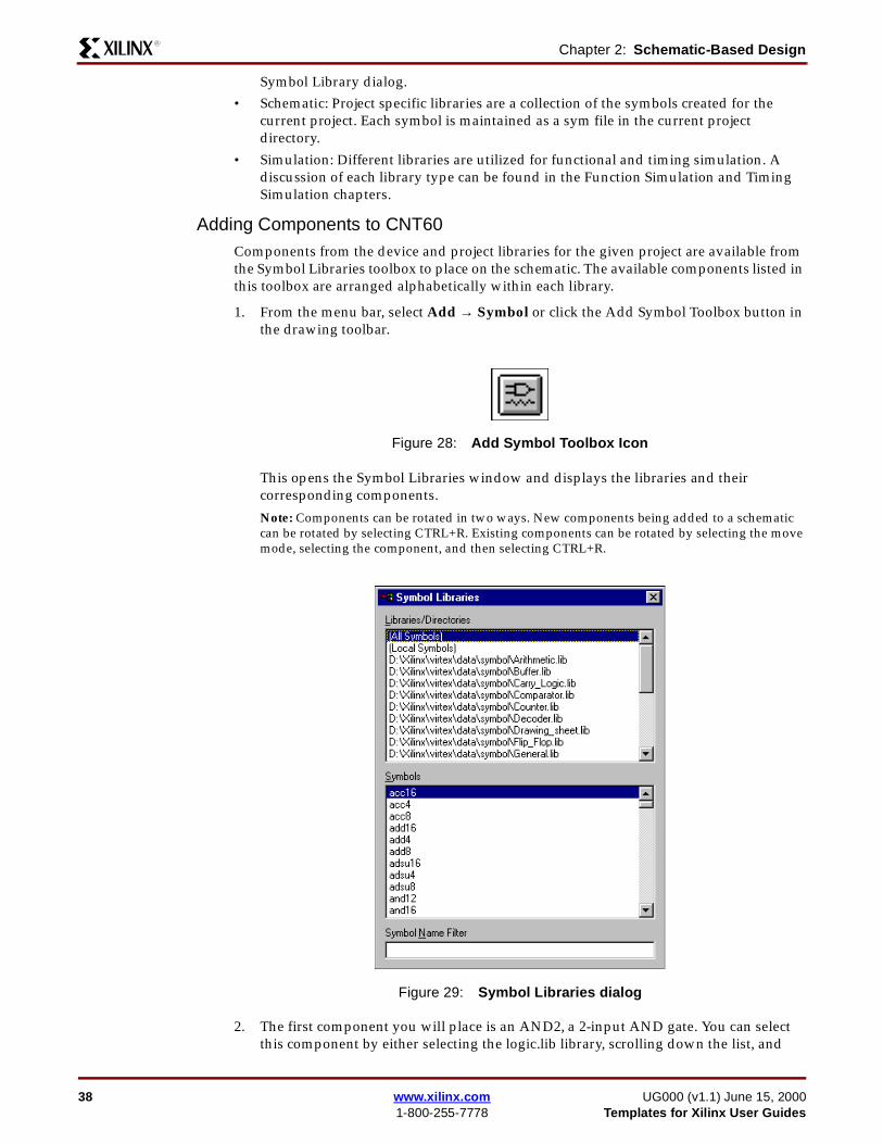
Chapter 2: Schematic-Based DesignR
Symbol Library dialog.• Schematic: Project specific libraries are a collection of the symbols created for the
current project. Each symbol is maintained as a sym file in the current project directory.
• Simulation: Different libraries are utilized for functional and timing simulation. A discussion of each library type can be found in the Function Simulation and Timing Simulation chapters.
Adding Components to CNT60Components from the device and project libraries for the given project are available from the Symbol Libraries toolbox to place on the schematic. The available components listed in this toolbox are arranged alphabetically within each library.
1. From the menu bar, select Add → Symbol or click the Add Symbol Toolbox button in the drawing toolbar.
This opens the Symbol Libraries window and displays the libraries and their corresponding components.
Note: Components can be rotated in two ways. New components being added to a schematic can be rotated by selecting CTRL+R. Existing components can be rotated by selecting the move mode, selecting the component, and then selecting CTRL+R.
2. The first component you will place is an AND2, a 2-input AND gate. You can select this component by either selecting the logic.lib library, scrolling down the list, and
Figure 28: Add Symbol Toolbox Icon
Figure 29: Symbol Libraries dialog
38 www.xilinx.com UG000 (v1.1) June 15, 20001-800-255-7778 Templates for Xilinx User Guides
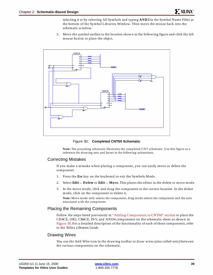
Chapter 2: Schematic-Based DesignR
selecting it or by selecting All Symbols and typing AND2 in the Symbol Name Filter at the bottom of the Symbol Libraries Window. Then move the mouse back into the schematic window.
3. Move the symbol outline to the location shown in the following figure and click the left mouse button to place the object.
Note: The preceding schematic illustrates the completed CNT schematic. Use this figure as a reference for drawing nets and buses in the following subsections.
Correcting MistakesIf you make a mistake when placing a component, you can easily move or delete the component.
1. Press the Esc key on the keyboard to exit the Symbols Mode.
2. Select Edit→ Delete or Edit→ Move. This places the editor in the delete or move mode
3. In the move mode, click and drag the component to the correct location. In the delete mode, click on the component to delete it.Note: Move mode only selects the component, drag mode selects the component and the nets associated with the component.
Placing the Remaining ComponentsFollow the steps listed previously in “Adding Components to CNT60” section to place the CD4CE, OR2, CB4CE, INV, and AND4 components on the schematic sheet as shown in Figure 30. For a detailed description of the functionality of each of these components, refer to the Xilinx Libraries Guide.
Drawing WiresYou use the Add Wire icon in the drawing toolbar to draw wires (also called nets) between the various components on the schematic.
Figure 30: Completed CNT60 Schematic
UG000 (v1.1) June 15, 2000 www.xilinx.com 39Templates for Xilinx User Guides 1-800-255-7778

Chapter 2: Schematic-Based DesignR
Signals can also logically be connected by naming multiple segments identically. In this case, the nets do not need to be physically connected on the schematic to make the logical connection. In the CNT60 schematic, you will draw wires to connect the components together. Do not yet worry about drawing the nets for the LSBSEC and MSBSEC buses. These nets will be drawn in the next section.
Follow these steps to draw a net between the AND2 and the CB4CE components on the CNT60 schematic.
1. Click the Add Wires icon in the drawing toolbar.
2. Click the source symbol pin (output pin of the AND2), then click on the destination pin (CE pin on the CB4CE). The net will automatically be drawn between the two pins. Note: You can specify the shape of the net by moving the mouse in the direction you want to draw the net and then single-clicking to create a 90-degree bend in the wire.
Draw the nets to connect the remaining components as shown in Figure 30, net names will be added in a later section. To draw a net between an already existing net and a pin, click once on the component pin and once on the existing net. A junction point will be drawn on the existing net.
You should now have all the nets drawn except those connected to the LSBSEC and MSBSEC buses. You will draw these in the next section.
Adding BusesIn ECS, a bus is simply a wire which has been given a multibit name. In order to add a bus follow the same methodolgy for adding wires and then add the proper name. Once a bus has been created you have the option to “tap” this bus off to use each signal individually. In this CNT60 schematic, you will create two buses, each comprised of the four output bits of each counter. These buses will be named LSBSEC[3:0] and MSBSEC[3:0], and they will also be connected to I/O markers to connect them to the CNT60 symbol.
Add buses to the schematic as follows.
1. Click the Add Wires icon in the drawing toolbar.
2. Click to the right of the CB4CE and draw a wire down and to the right of the symbol. Refer to the completed schematic for the exact positioning.
3. Terminate the wire by either double clicking with the left mouse button, or single-clicking with the right mouse button.
4. To change the wire into a bus, the wire must be named. Select the Add Net Name icon in the drawing toolbar. With the keyboard enter msbsec(3:0) and hit enter. This will attach the bus name to the cursor. Click on the end of the bus to apply the name. This will change the wire into a bus. To verify this, zoom in, the bus is represented visually by a thicker wire.
Figure 31: Add Wires Icon
Figure 32: Add Net Name Icon
40 www.xilinx.com UG000 (v1.1) June 15, 20001-800-255-7778 Templates for Xilinx User Guides
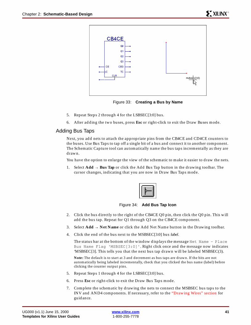
Chapter 2: Schematic-Based DesignR
5. Repeat Steps 2 through 4 for the LSBSEC[3:0] bus.
6. After adding the two buses, press Esc or right-click to exit the Draw Buses mode.
Adding Bus TapsNext, you add nets to attach the appropriate pins from the CB4CE and CD4CE counters to the buses. Use Bus Taps to tap off a single bit of a bus and connect it to another component. The Schematic Capture tool can automatically name the bus taps incrementally as they are drawn.
You have the option to enlarge the view of the schematic to make it easier to draw the nets.
1. Select Add → Bus Tap or click the Add Bus Tap button in the drawing toolbar. The cursor changes, indicating that you are now in Draw Bus Taps mode.
2. Click the bus directly to the right of the CB4CE Q0 pin, then click the Q0 pin. This will add the bus tap. Repeat for Q1 through Q3 on the CB4CE component.
3. Select Add → Net Name or click the Add Net Name button in the Drawing toolbar.
4. Click the end of the bus next to the MSBSEC[3:0] bus label.
The status bar at the bottom of the window displays the message Net Name - Place Bus Name Flag ‘MSBSEC[3:0]’. Right click once and the message now indicates ‘MSBSEC[3]. This tells you that the next bus tap drawn will be labeled MSBSEC(3).
Note: The default is to start at 3 and decrement as bus taps are drawn. If the bits are not automatically being labeled incrementally, check that you clicked the bus name (label) before clicking the counter output pins.
5. Repeat Steps 1 through 4 for the LSBSEC[3:0] bus.
6. Press Esc or right-click to exit the Draw Bus Taps mode.
7. Complete the schematic by drawing the nets to connect the MSBSEC bus taps to the INV and AND4 components. If necessary, refer to the “Drawing Wires” section for guidance.
Figure 33: Creating a Bus by Name
Figure 34: Add Bus Tap Icon
UG000 (v1.1) June 15, 2000 www.xilinx.com 41Templates for Xilinx User Guides 1-800-255-7778
Chapter 2: Schematic-Based DesignR
8. Compare your CNT60 schematic again with Figure 30 to ensure that all connections are properly made.Note: If the nets appear disconnected, try selecting View → Redraw to refresh the screen.
Adding Net NamesNext, you add net names to the CLK, CLR, and CE nets.
1. Select Add → Net Name or click the Add Net Name button in the Drawing toolbar.
2. At the bottom of the schematic editor the following is displayed: “Net Name - Enter Net Name =”. Enter “CLK” and hit return.
3. The net name clk is now attached to the cursor. Click on the end of the CLK net. The name is then attached to the end of the net. If the net name is not attached to the end of the net but appears above the net, delete the net name and repeat the process.
4. Repeat steps 1-3 for CE and CLR.
Adding I/O MarkersI/O markers are used to determine the ports on a macro or the top level schematic. Add I/O markers to the cnt60 schematic to determine the macro ports.
Follow these steps to add the I/O markers as shown in Figure 30.
1. Select Add→ I/O Marker. This will open the I/O marker dialog. Select input.
2. Click and drag a box around the following nets: clk, ce, and clr.
3. Change the marker type to output and add a marker to the msbsec(3:0) and lsbsec(3:0) nets.
Saving the SchematicThe CNT60 schematic is now complete.
Save the schematic by selecting File → Save or clicking the Save icon in the horizontal toolbar.
Creating the cnt60 symbolThe symbol representing the cnt60 schematic will now be created in Project Navigator.
1. In the Source Window, select cnt60.sch
2. In the Process Window expand the Design Entry Utilities tree by click on the +.
3. Double click on Create Schematic Symbol.
Placing the CNT60 MacroSo far, you have created the CNT60 macro. The next step is to place this macro on the top-level Watch schematic sheet, where it may then be connected to other components in the design.
1. Open the Watch schematic sheet by double clicking on stopwatch.sch in the Source Window.
Figure 35: Save Icon
42 www.xilinx.com UG000 (v1.1) June 15, 20001-800-255-7778 Templates for Xilinx User Guides
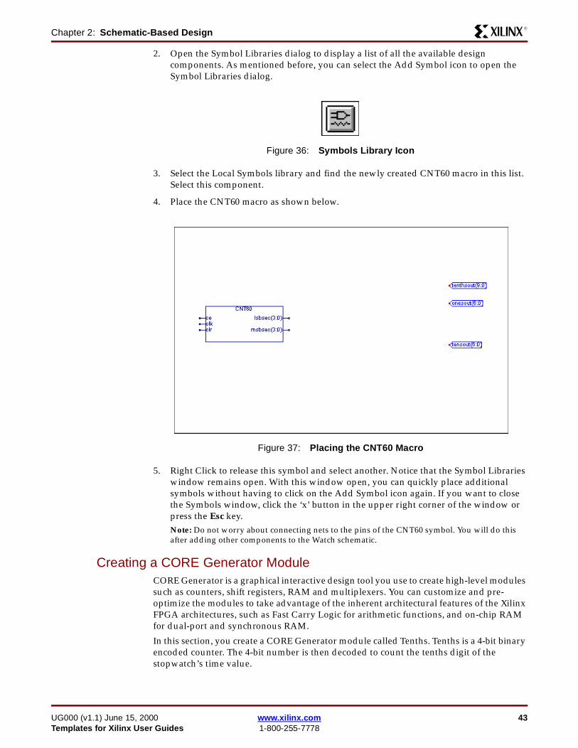
Chapter 2: Schematic-Based DesignR
2. Open the Symbol Libraries dialog to display a list of all the available design components. As mentioned before, you can select the Add Symbol icon to open the Symbol Libraries dialog.
3. Select the Local Symbols library and find the newly created CNT60 macro in this list. Select this component.
4. Place the CNT60 macro as shown below.
5. Right Click to release this symbol and select another. Notice that the Symbol Libraries window remains open. With this window open, you can quickly place additional symbols without having to click on the Add Symbol icon again. If you want to close the Symbols window, click the ‘x’ button in the upper right corner of the window or press the Esc key. Note: Do not worry about connecting nets to the pins of the CNT60 symbol. You will do this after adding other components to the Watch schematic.
Creating a CORE Generator ModuleCORE Generator is a graphical interactive design tool you use to create high-level modules such as counters, shift registers, RAM and multiplexers. You can customize and pre-optimize the modules to take advantage of the inherent architectural features of the Xilinx FPGA architectures, such as Fast Carry Logic for arithmetic functions, and on-chip RAM for dual-port and synchronous RAM.
In this section, you create a CORE Generator module called Tenths. Tenths is a 4-bit binary encoded counter. The 4-bit number is then decoded to count the tenths digit of the stopwatch’s time value.
Figure 36: Symbols Library Icon
Figure 37: Placing the CNT60 Macro
UG000 (v1.1) June 15, 2000 www.xilinx.com 43Templates for Xilinx User Guides 1-800-255-7778

Chapter 2: Schematic-Based DesignR
Creating the Core Generator ModuleYou select the type of module you want in the CORE Generator dialog box as well as the specific features of the module. You can invoke this GUI from the Project Navigator New Source Wizard.
1. In Project Navigator select Project→ New Source.
2. Select Coregen IP, enter tenths in the File Name field and click Next and Finish.
3. The Xilinx CORE Generator 3.1i opens and displays a list of possible COREs available. Double Click on Basic Elements - Counters.
4. Double Click on Binary Counter to open the Binary Counter dialog. This dialog allows the user to customize the counter to the design specifications.
5. Fill in the Binary Counter dialog with the following settings.
- Component Name: TenthsDefines the name of the module.
- Output Width: 4Defines the width of the output bus.
- Operation: UpDefines how the counter will operate. This field is dependant on the type of module you select.
- Count Restrictions: Restrict Count to A. This dictates the maximum count value.
- Output Options: Threshold0 set to ASignal goes high when the value specified has been reached.
- Output Options: Registered
6. Click on the Register Options button to open the Register Options dialog. Enter the following settings.
- Clock Enable: Selected- Asynchronous Settings: Init with a value of 1.
- Synchronous Settings: None- Click Ok.
7. Check that only the following pins are used.
- AINIT- CE
- Q- Q_Thresh0
44 www.xilinx.com UG000 (v1.1) June 15, 20001-800-255-7778 Templates for Xilinx User Guides

Chapter 2: Schematic-Based DesignR
8. Click Generate. The module is created and automatically added to the project library.
A number of files are added to the project directory. These files are:
• TENTHS.EDNThis file is the netlist that is used during the Translate phase of implementation.
• TENTHS.VHO or TENTHS.VEOThis is the instantiation template that is used to incorporate the CORE Generator module in your source HDL.
• TENTHS.XCOThis file stores the configuration information for the Tenths module.
• COREGEN.PRJThis file stores the Coregen configuration for the project.
9. Select Cancel and close Core Generator.
Creating a State Machine ModuleWith VSS State CAD, you graphically create finite state machines. You draw states, inputs/outputs, and state transition conditions on the diagram using a simple windows GUI. Transition conditions and state actions are typed into the diagram using language independent syntax. The State Editor then exports the diagram to either VHDL, Verilog or ABEL code. The resulting HDL file is finally synthesized to create a netlist and/or macro for you to place on a schematic sheet.
For this tutorial, a partially complete state machine diagram is provided. In the next section, you complete the diagram and synthesize the module into a macro to place on the
Figure 38: CoreGen Module Selector
UG000 (v1.1) June 15, 2000 www.xilinx.com 45Templates for Xilinx User Guides 1-800-255-7778
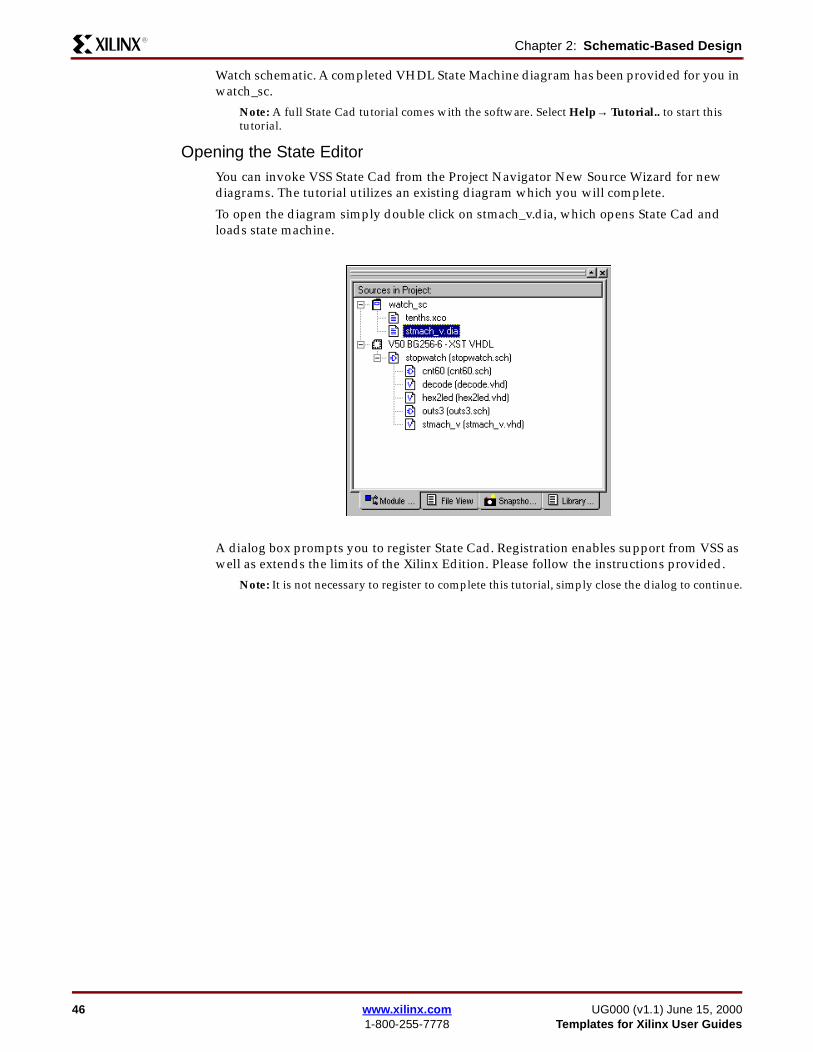
Chapter 2: Schematic-Based DesignR
Watch schematic. A completed VHDL State Machine diagram has been provided for you in watch_sc.
Note: A full State Cad tutorial comes with the software. Select Help→ Tutorial.. to start this tutorial.
Opening the State EditorYou can invoke VSS State Cad from the Project Navigator New Source Wizard for new diagrams. The tutorial utilizes an existing diagram which you will complete.
To open the diagram simply double click on stmach_v.dia, which opens State Cad and loads state machine.
A dialog box prompts you to register State Cad. Registration enables support from VSS as well as extends the limits of the Xilinx Edition. Please follow the instructions provided.
Note: It is not necessary to register to complete this tutorial, simply close the dialog to continue.
46 www.xilinx.com UG000 (v1.1) June 15, 20001-800-255-7778 Templates for Xilinx User Guides

Chapter 2: Schematic-Based DesignR
The unfinished State Machine diagram is shown below.
• The circles represent the various states.
• The black expressions are the transition conditions, defining how you move between states.
• The output expressions for each state are contained in the circle representing the state.
In the state machine diagrams, the transition conditions and the state actions are written in language independent syntax and then exported to Verilog, VHDL, or ABEL.
In the following section, you add the remaining states, transitions, actions, and also a reset condition to complete the state machine.
Adding New StatesComplete the state machine by adding a new state called CLEAR.
1. Click the Draw State icon in the vertical toolbar.
The state bubble is now attached to the cursor.
2. Place the new state on the left-hand side of the diagram as shown below. Click the mouse to place the state bubble.
3. The state is given a default name, in this case STATE0. Double click the STATE0 in the state bubble, and change the name of the state to CLEAR.. The name of the state is for your use only; it does not affect the synthesis, and so you can name it whatever you want.
Figure 39: Incomplete State Machine Diagram
Figure 40: Draw State Icon
UG000 (v1.1) June 15, 2000 www.xilinx.com 47Templates for Xilinx User Guides 1-800-255-7778

Chapter 2: Schematic-Based DesignR
4. Click Ok.
You can change the shape of the state bubble by clicking the bubble and dragging in the direction to “stretch” the bubble.
Adding a TransitionA transition defines the movement between states of the state machine. Transitions are represented by arrows in the editor. You will be adding a transition from the CLEAR state to the ZERO state in the following steps. Because this transition is unconditional, there is no Transition Condition associated with it.
1. Click the Draw Transitions icon in the vertical toolbar.
Figure 41: Adding the CLEAR State
Figure 42: Draw Transistions Icon
48 www.xilinx.com UG000 (v1.1) June 15, 20001-800-255-7778 Templates for Xilinx User Guides
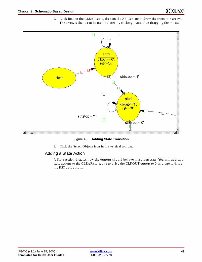
Chapter 2: Schematic-Based DesignR
2. Click first on the CLEAR state, then on the ZERO state to draw the transition arrow. The arrow’s shape can be manipulated by clicking it and then dragging the mouse.
3. Click the Select Objects icon in the vertical toolbar.
Adding a State ActionA State Action dictates how the outputs should behave in a given state. You will add two state actions to the CLEAR state, one to drive the CLKOUT output to 0, and one to drive the RST output to 1.
Figure 43: Adding State Transition
UG000 (v1.1) June 15, 2000 www.xilinx.com 49Templates for Xilinx User Guides 1-800-255-7778

Chapter 2: Schematic-Based DesignR
1. Double Click on the State. This opens the Edit State dialog which allows use to create the desired outputs.
2. Select the Output Wizard.
3. In the Output Wizard, select the following:
DOUT = clkout, CONSTANT = ‘0’;
DOUT = rst, CONSTANT = ‘1’;
You must click Ok, each time to enter the value.
Figure 44: Edit State Dialog
50 www.xilinx.com UG000 (v1.1) June 15, 20001-800-255-7778 Templates for Xilinx User Guides
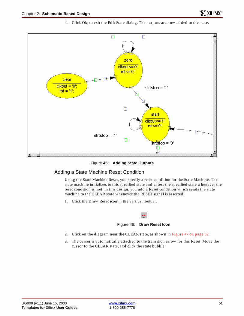
Chapter 2: Schematic-Based DesignR
4. Click Ok, to exit the Edit State dialog. The outputs are now added to the state.
Adding a State Machine Reset ConditionUsing the State Machine Reset, you specify a reset condition for the State Machine. The state machine initializes to this specified state and enters the specified state whenever the reset condition is met. In this design, you add a Reset condition which sends the state machine to the CLEAR state whenever the RESET signal is asserted.
1. Click the Draw Reset icon in the vertical toolbar.
2. Click on the diagram near the CLEAR state, as shown in Figure 47 on page 52.
3. The cursor is automatically attached to the transition arrow for this Reset. Move the cursor to the CLEAR state, and click the state bubble.
Figure 45: Adding State Outputs
Figure 46: Draw Reset Icon
UG000 (v1.1) June 15, 2000 www.xilinx.com 51Templates for Xilinx User Guides 1-800-255-7778

Chapter 2: Schematic-Based DesignR
4. A question is then asked, “Should this reset be asynchronous(Yes) or synchronous(No)?” Please answer yes.
5. Save your changes by selecting File → Save.
Creating the State Machine MacroYou will now create the HDL code used to create a macro symbol that you can place on the Watch schematic. The macro symbol will automatically be added to the project library. Creation of the macro includes the creation of the HDL code from the state machine diagram.
1. Select Options→ Compile(Generate HDL). State Cad verifies the state machine and displayes the results. Review the results and close the dialog.
2. State Cad will then create the HDL code and open a browser displaying the code. Close the browser when you have finished examining the code.
3. Close State CAD.
4. In Project Navigator select Project→ Add Source and select stmach_v.vhd which is the VHDL file generated by State Cad. Select VHDL module as the source type.
5. Once stmach_v.vhd has been added to the project, select stmach_v.vhd, then double click on Create Schematic Symbol under the Design Entry Utilities in the Process Window.
Placing the STMACH, Tenths, and decode symbolsYou can now place the STMACH, Tenths, and decode symbols on the Watch schematic. If it is not already opened, open the Schematic Editor. Open the Symbol Libraries window to
Figure 47: Adding Reset
52 www.xilinx.com UG000 (v1.1) June 15, 20001-800-255-7778 Templates for Xilinx User Guides
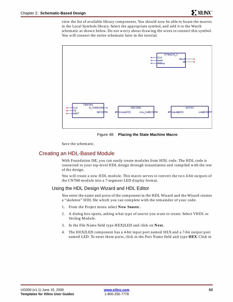
Chapter 2: Schematic-Based DesignR
view the list of available library components. You should now be able to locate the macros in the Local Symbols library. Select the appropriate symbol, and add it to the Watch schematic as shown below. Do not worry about drawing the wires to connect this symbol. You will connect the entire schematic later in the tutorial.
Save the schematic.
Creating an HDL-Based ModuleWith Foundation ISE, you can easily create modules from HDL code. The HDL code is connected to your top-level HDL design through instantiation and compiled with the rest of the design.
You will create a new HDL module. This macro serves to convert the two 4-bit outputs of the CNT60 module into a 7-segment LED display format.
Using the HDL Design Wizard and HDL EditorYou enter the name and ports of the component in the HDL Wizard and the Wizard creates a “skeleton” HDL file which you can complete with the remainder of your code.
1. From the Project menu select New Source.
2. A dialog box opens, asking what type of source you want to create. Select VHDL or Verilog Module.
3. In the File Name field type HEX2LED and click on Next.
4. The HEX2LED component has a 4-bit input port named HEX and a 7-bit output port named LED. To enter these ports, click in the Port Name field and type HEX. Click in
Figure 48: Placing the State Machine Macro
UG000 (v1.1) June 15, 2000 www.xilinx.com 53Templates for Xilinx User Guides 1-800-255-7778
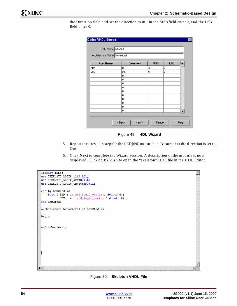
Chapter 2: Schematic-Based DesignR
the Direction field and set the direction to in. In the MSB field enter 3, and the LSB field enter 0.
5. Repeat the previous step for the LED[6:0] output bus. Be sure that the direction is set to Out.
6. Click Next to complete the Wizard session. A description of the module is now displayed. Click on Finish to open the “skeleton” HDL file in the HDL Editor.
Figure 49: HDL Wizard
Figure 50: Skeleton VHDL File
54 www.xilinx.com UG000 (v1.1) June 15, 20001-800-255-7778 Templates for Xilinx User Guides
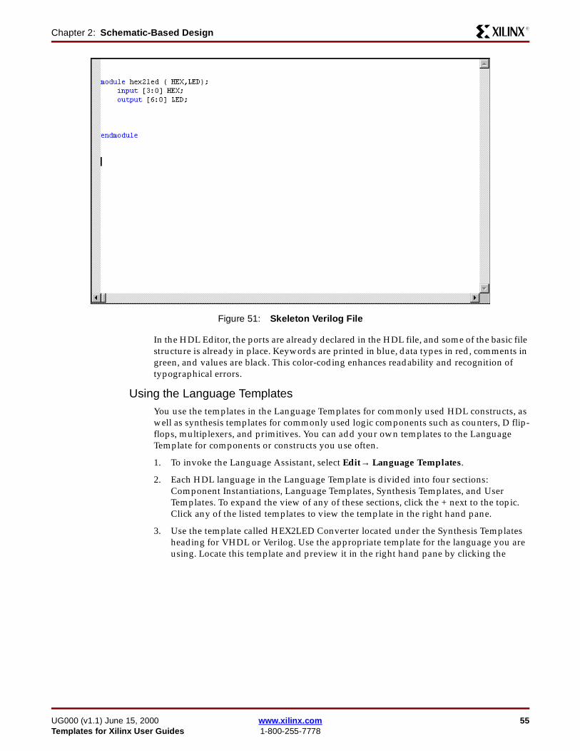
Chapter 2: Schematic-Based DesignR
In the HDL Editor, the ports are already declared in the HDL file, and some of the basic file structure is already in place. Keywords are printed in blue, data types in red, comments in green, and values are black. This color-coding enhances readability and recognition of typographical errors.
Using the Language TemplatesYou use the templates in the Language Templates for commonly used HDL constructs, as well as synthesis templates for commonly used logic components such as counters, D flip-flops, multiplexers, and primitives. You can add your own templates to the Language Template for components or constructs you use often.
1. To invoke the Language Assistant, select Edit→ Language Templates.
2. Each HDL language in the Language Template is divided into four sections: Component Instantiations, Language Templates, Synthesis Templates, and User Templates. To expand the view of any of these sections, click the + next to the topic. Click any of the listed templates to view the template in the right hand pane.
3. Use the template called HEX2LED Converter located under the Synthesis Templates heading for VHDL or Verilog. Use the appropriate template for the language you are using. Locate this template and preview it in the right hand pane by clicking the
Figure 51: Skeleton Verilog File
UG000 (v1.1) June 15, 2000 www.xilinx.com 55Templates for Xilinx User Guides 1-800-255-7778
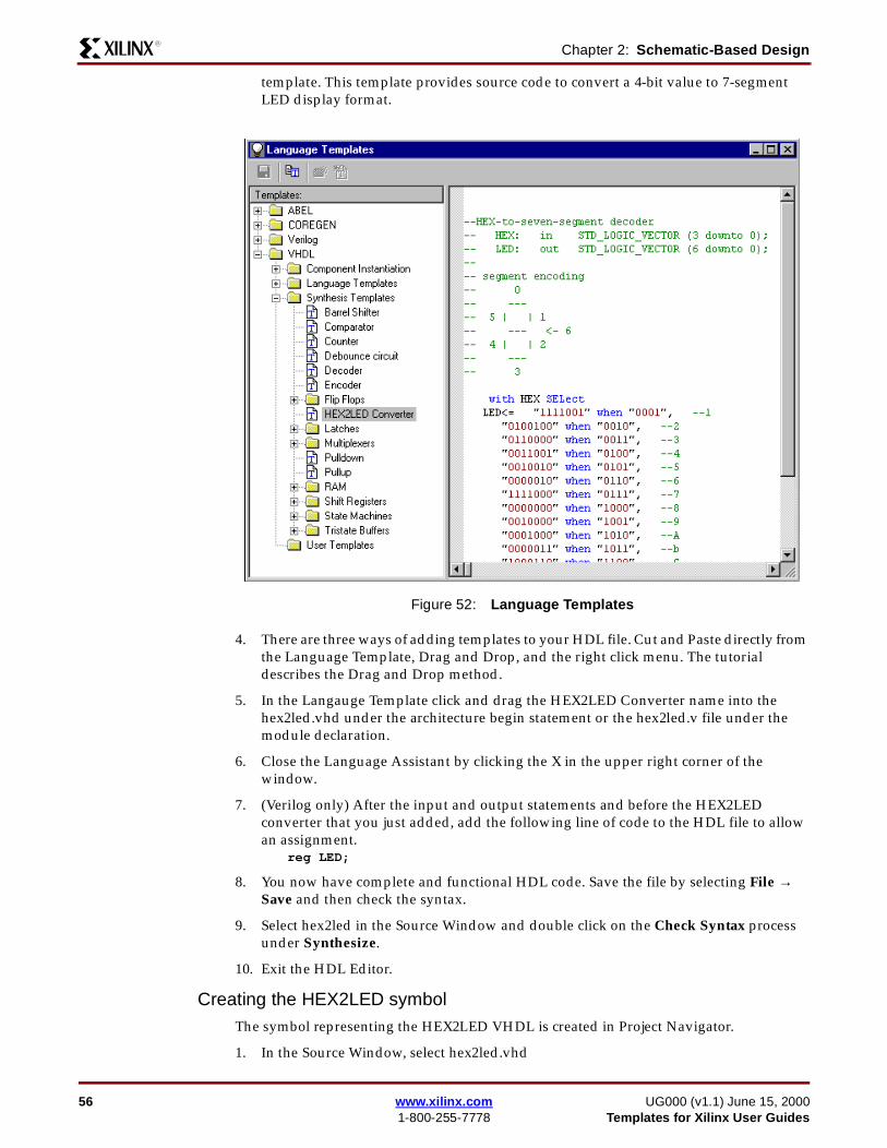
Chapter 2: Schematic-Based DesignR
template. This template provides source code to convert a 4-bit value to 7-segment LED display format.
4. There are three ways of adding templates to your HDL file. Cut and Paste directly from the Language Template, Drag and Drop, and the right click menu. The tutorial describes the Drag and Drop method.
5. In the Langauge Template click and drag the HEX2LED Converter name into the hex2led.vhd under the architecture begin statement or the hex2led.v file under the module declaration.
6. Close the Language Assistant by clicking the X in the upper right corner of the window.
7. (Verilog only) After the input and output statements and before the HEX2LED converter that you just added, add the following line of code to the HDL file to allow an assignment.
reg LED;
8. You now have complete and functional HDL code. Save the file by selecting File → Save and then check the syntax.
9. Select hex2led in the Source Window and double click on the Check Syntax process under Synthesize.
10. Exit the HDL Editor.
Creating the HEX2LED symbolThe symbol representing the HEX2LED VHDL is created in Project Navigator.
1. In the Source Window, select hex2led.vhd
Figure 52: Language Templates
56 www.xilinx.com UG000 (v1.1) June 15, 20001-800-255-7778 Templates for Xilinx User Guides

Chapter 2: Schematic-Based DesignR
2. In the Process Window expand the Design Entry Utilities tree by click on the +.
3. Double click on Create Schematic Symbol.
Adding the HEX2LED Component to the SchematicYou are now ready to place the HEX2LED macro on the Watch schematic. Open the Schematic Editor if it is not already open. Open the Symbols Libraries dialog (refer to “Adding Components to CNT60” section) to view the list of available library components. You should now be able to locate the HEX2LED macro in this list. Select it, and add it to the Watch schematic as shown in the next figure.
This component will be placed on the Watch schematic sheet in two separate instances. To duplicate the component in the schematic, click the left mouse button while the pointer is on the placed symbol, and then click again to place the duplicate symbol.
Note: The Symbol Libraries icon must still be depressed on the drawing toolbar to enable this feature to automatically duplicate a symbol.
Again, do not worry about drawing the wires and buses to connect this macro. You will connect the entire schematic later in the tutorial.
Specifying Device Inputs/OutputsWhen specifying device I/O on a schematic sheet, use the I/O Marker. All ECS schematics are netlisted to VHDL or Verilog and then synthesized by the synthesis tool of choice. When the synthesis tool synthesizes the top level HDL, the I/O markers are replaced with the appropriate pads and buffers.
Note: I/O components are contained in the Xilinx Unified Library and can be added to the schematic sheet, however special considerations must be made.
1. I/O macros are not recognized by the synthesis tool, therefore a duplicate buffer will be inserted. To avoid this use I/O primitives only.
2. Global buffers, for example BUFG, are not recognized by the implementation tools, therefore a pad is not inserted and the logic is trimmed. To avoid this place a IBUF in front of the BUFG.
Hierarchy Push/PopDescend into a lower-level of hierarchy to view the underlying file. You will be pushing down into the OUTS3 macro, which is a schematic-based user-created macro.
Figure 53: Placing the HEX2LED Component
UG000 (v1.1) June 15, 2000 www.xilinx.com 57Templates for Xilinx User Guides 1-800-255-7778
Chapter 2: Schematic-Based DesignR
1. To push down into OUTS3, click the Hierarchy Push/Pop button. The cursor changes to a cross hairs. Click the OUTS3 symbol.
In the OUTS3 schematic, you see a series of inverters (INV) and output buffers (OBUF). This macro illustrates that you can place I/O buffers in a lower level macro. The output buffers are not required because the synthesis tool will insert buffers if one is not found.
2. “Pop” back out of the OUTS3 component by selecting the Hierarchy Push/Pop icon, then click in an empty space in the OUTS3 schematic to return to the top-level Watch schematic sheet.
Adding Input PinsAdd three more input pins to the Watch schematic, called CLK, RESET and STRTSTOP.
1. Add an IBUF for each of the two input pins, RESET and STRTSTOP. Add an IBUF and a BUFG for the input clock signal, CLK. To add these components, click the Symbol Libraries icon in the vertical toolbar to open the Symbol Libraries dialog. Browse to locate the IBUF, INV, and BUFG components in the library. Drop these on the schematic as shown below.
2. Draw a net between the IBUF, INV, and BUFG inputs and outputs. If necessary, refer to the section on drawing nets (see the “Drawing Wires” section) for instructions.
Figure 54: Hierarchy Push/Pop Icon
Figure 55: OUTS3 Schematic Macro
58 www.xilinx.com UG000 (v1.1) June 15, 20001-800-255-7778 Templates for Xilinx User Guides

Chapter 2: Schematic-Based DesignR
3. Draw a net to the input of each IBUF.
Adding I/O Markers and Net NamesIt is important to label nets and buses for several reasons. It aids in debugging and simulation, as you will more easily trace nets back to your original design. Any nets which remain unnamed in the design will be given machine-generated names which will mean nothing to you later in the implementation process. Naming nets also enhances readability and aids in documenting your design.
Label the three input nets you just drew as illistrated in the completed schematic.
1. Select Add→ Net Name.
2. At the bottom of the ECS you will see the following: ‘Net Name - Enter Net Name =’ type RESET and hit Enter.
3. The net name is now attached to the cursor. Place the name on the leftmost end of the net as illistrated in Figure 59 on page 60.
4. Repeat Steps 1 through 3 for the STRTSTOP and CLK pins.
5. Once all of the nets have been labeled add the I/O marker. Select Add→ I/O Marker.
Figure 56: Placing CLK, RESET and STRTSTOP I/O Components
Figure 57: Labeling Nets
UG000 (v1.1) June 15, 2000 www.xilinx.com 59Templates for Xilinx User Guides 1-800-255-7778

Chapter 2: Schematic-Based DesignR
6. In the I/O marker dialog, select input then draw a box around the three labeled nets.
Assigning Pin LocationsXilinx recommends that you let the automatic placement and routing program, PAR, define the pinout of your design. Pre-assigning locations to the pins can sometimes degrade the performance of the place and route tools. However, it is usually necessary, at some point, to lock the pinout of a design so that it can be integrated into a PCB (Printed Circuit Board).
Define the initial pinout by running the place-and-route tools without pin assignments, then locking down the pin placement so that it reflects the locations chosen by the tools. Because this design is simple and timing is not critical, the example pin assignments will not adversely affect the ability of PAR to place and route the design.
Specify pin locations by attaching a LOC parameter to a buffer component or I/O net. Assign a LOC parameter to the RESET net on the Watch schematic as follows.
1. Select Edit→ Attribute→ Net Attribute. The Net Attribute Editor opens.
Figure 58: Adding I/O Markers
Figure 59: Labeled Nets
60 www.xilinx.com UG000 (v1.1) June 15, 20001-800-255-7778 Templates for Xilinx User Guides

Chapter 2: Schematic-Based DesignR
2. Select the RESET net on the schematic.
3. In the Net Attribute Editor select PlaceAnd Route and enter the following value: LOC=”A2”
The quotation marks are required. This step assigns the RESET signal to pin A2 of the target device.
4. To view the location constraint on the net add a net attribute window. Select Edit→ Attribute→ Net Attribute Window. Then select the RESET net.
5. Repeat Steps 1 through 4 to assign the STRTSTOP input to pin A5 and the CLK input to pin A3.
Completing the SchematicComplete the schematic by wiring the components you have created and placed, adding any additional necessary logic, and labeling nets appropriately. The following steps guide you through the process of completing the schematic, or you may want to use the completed schematic shown below for guidance. Each of the actions in this section has been discussed in detail in earlier sections of the tutorial. If you need to review these
Figure 60: Assigning Pin Locations
UG000 (v1.1) June 15, 2000 www.xilinx.com 61Templates for Xilinx User Guides 1-800-255-7778
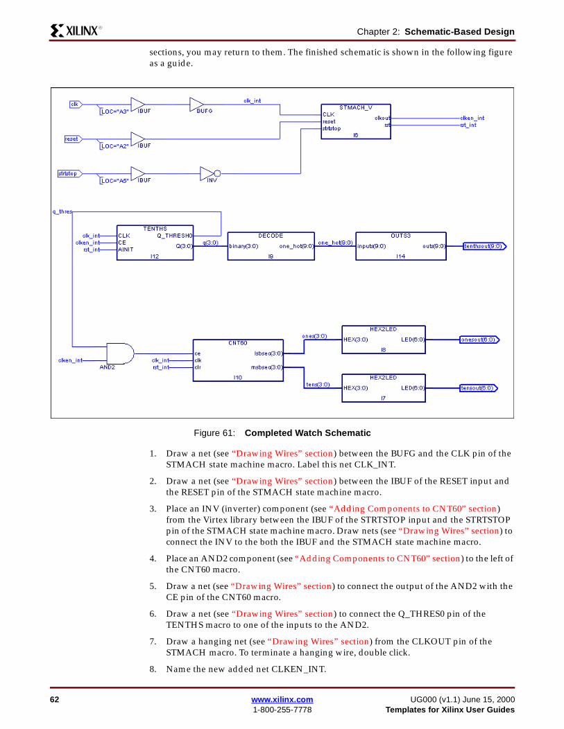
Chapter 2: Schematic-Based DesignR
sections, you may return to them. The finished schematic is shown in the following figure as a guide.
1. Draw a net (see “Drawing Wires” section) between the BUFG and the CLK pin of the STMACH state machine macro. Label this net CLK_INT.
2. Draw a net (see “Drawing Wires” section) between the IBUF of the RESET input and the RESET pin of the STMACH state machine macro.
3. Place an INV (inverter) component (see “Adding Components to CNT60” section) from the Virtex library between the IBUF of the STRTSTOP input and the STRTSTOP pin of the STMACH state machine macro. Draw nets (see “Drawing Wires” section) to connect the INV to the both the IBUF and the STMACH state machine macro.
4. Place an AND2 component (see “Adding Components to CNT60” section) to the left of the CNT60 macro.
5. Draw a net (see “Drawing Wires” section) to connect the output of the AND2 with the CE pin of the CNT60 macro.
6. Draw a net (see “Drawing Wires” section) to connect the Q_THRES0 pin of the TENTHS macro to one of the inputs to the AND2.
7. Draw a hanging net (see “Drawing Wires” section) from the CLKOUT pin of the STMACH macro. To terminate a hanging wire, double click.
8. Name the new added net CLKEN_INT.
Figure 61: Completed Watch Schematic
62 www.xilinx.com UG000 (v1.1) June 15, 20001-800-255-7778 Templates for Xilinx User Guides

Chapter 2: Schematic-Based DesignR
9. Draw a hanging net at the CLK_EN input pin of the TENTHS macro. Label this net CLKEN_INT (see “Adding I/O Markers and Net Names” on page 59).
10. Draw a hanging net (see “Drawing Wires” section) at the other input of the AND2 component. Label this net CLKEN_INT again (see the“” section).
11. Draw a hanging net (see “Drawing Wires” section) from the RST output pin of the STMACH macro. Label this net RST_INT.
12. Draw two more hanging nets (see “Drawing Wires” section), also named RST_INT, from the AINIT pin of the TENTHS macro and from the CLR pin of the CNT60 macro.
13. Draw two hanging nets (see “Drawing Wires” section), each named CLK_INT, from the CLOCK pin of the TENTHS macro and from the CLK pin of the CNT60 macro.Note: Remember that nets are logically connected if their names are the same, even if the net is not physically drawn as a connection in the schematic. This method is used to make the logical connection of the RST_INT, CLKEN_INT and CLK_INT signals.
14. Draw buses (see “Adding Buses” on page 40) to complete the schematic. Label them as shown on the preceding schematic diagram.
The schematic is now complete!
15. Save the design by selecting File → Save.
UG000 (v1.1) June 15, 2000 www.xilinx.com 63Templates for Xilinx User Guides 1-800-255-7778

Chapter 2: Schematic-Based DesignR
64 www.xilinx.com UG000 (v1.1) June 15, 20001-800-255-7778 Templates for Xilinx User Guides
R
Chapter 3
Functional Simulation
You can perform functional simulation before design implementation to verify that the logic that you have created is correct. Foundation ISE provides integration with any Modelsim Simulator. You can perform behavioural simulation on a schematic-based or HDL-based design. In a later section, you can perform timing simulation, which takes place after the design is implemented (placed and routed) with the Xilinx Implementation Tools.
This chapter contains the following sections.
• “Starting HDL Bencher”• “Starting Modelsim”
• “Adding Signals”• “Saving the Simulation”
• “Restarting the Simulation”
Starting HDL BencherHDL Bencher is a testbench/test fixture creation tool from Visual Software Solutions (VSS). It allows the user to graphically enter stimulas and expected response, then generates a VHDL or Verilog testbench.
For installation information see the Foundation ISE Installation Guide.
Creating StimulasUse the following procedure to create a testbench/test fixture with HDL Bencher.
1. Select a VHDL, Verilog, or Schematic source file in the Source Window.
2. Double click on Launce HDL Bencher Tool under Design Entry Utilities in the Process Window.
3. This opens HDL Bencher and loads the selected source file.
4. HDL Bencher opens the Initialize Timing dialog which allows the selection of the Master Clock and Clock Timing. For the purpose of the tutorial, the defaults will be used. Click Ok.
UG000 (v1.1) June 15, 2000 www.xilinx.com 65Templates for Xilinx User Guides 1-800-255-7778

Chapter 3: Functional SimulationR
HDL Bencher contains two main windows. The top window is the Waveform Window. In this window the user graphically enters the stimulas and expected response. The bottom window is the currently loaded HDL file.
5. Click the reset cell below clk cycle 1 to set it high.
6. Click the reset cell below clk cycle 5 to set it low.
7. Click the strtstop cell below clk cycle 30 to set it high.
8. Click the strtstop cell below clk cycle 33 to set it low.
9. Click the strtstop cell below clk cycle 39 to set it high.
10. Click the strtstop cell below clk cycle 41 to set it low.
11. Select the Save Waveform button.
Specifying Expected ResponseHDL Bencher provides the ability to enter the expected respose for any output. The simulator then verifies the expected response verses the actual response and flags any errors.
Figure 62: HDL Bencher windows
66 www.xilinx.com UG000 (v1.1) June 15, 20001-800-255-7778 Templates for Xilinx User Guides

Chapter 3: Functional SimulationR
Use the following procedure to enter the expected response for this design. The expected response is entered in the yellow box below each clk cycle.
1. Click the tensout cell below clk cycle 1 and enter 1000000.
2. Click the onesout cell below clk cycle 1 and enter 1000000.
3. Using the information in Figure 63, enter the rest of the expected response.
Creating a Test BenchOnce the stimulas and expected response have been completed HDL Bencher will create a testbench. Select File→ Export Testbench to generate and view the testbench. Exit the testbench viewer and HDL Bencher.
Adding the Test Bench to the ProjectIn Project Navigator select Project→ Add Source and browse for watch_tb.vhd. When a new VHDL source is added to the project, Project Navigator requires the user to select the source type. If the source type is a test bench, the user is asked to associate the test bench with a source file. For the purpose of adding the testbench select the source type as testbench and the associated source as watch.
The waveform information for the testbench in stored in watch_tb.tbw. Add this file to the project. You can open HDL Bencher by double clicking on this file in the future.
Since this tutorial utilizes a Core Generator Core some additional information must be added to the testbench for simulation. In Project Navigator select File→ Open and browse for config.vhd.
The file is broken into two sections, VHDL and schematic. In both cases double click on the test bench in the source window. Copy the appropriate section of config.vhd and replace the configuration at the end of the test bench. Save and close the modified test bench.
Note: Each time the test bench is exported, the configuration information is lost and must be added again.
Starting ModelsimFoundation ISE has full integrated any version of the Modelsim Simulator. Foundation ISE provides work directory creation, source file compilation, simulation initialization, and control over simulation properties.
Figure 63: Expected Response
UG000 (v1.1) June 15, 2000 www.xilinx.com 67Templates for Xilinx User Guides 1-800-255-7778
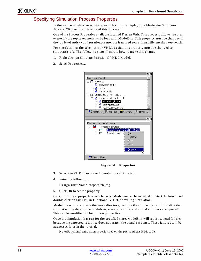
Chapter 3: Functional SimulationR
Specifying Simulation Process PropertiesIn the source window select stopwatch_tb.vhd this displays the ModelSim Simulator Process. Click on the + to expand this process.
One of the Process Properties available is called Design Unit. This property allows the user to specify the top level model to be loaded in ModelSim. This property must be changed if the top level entity, configuration, or module is named something different than testbench.
For simulation of the schematic or VHDL design this property must be changed to stopwatch_cfg. The following steps illustrate how to make this change:
1. Right click on Simulate Functional VHDL Model.
2. Select Properties...
3. Select the VHDL Functional Simulation Options tab.
4. Enter the following:
Design Unit Name: stopwatch_cfg
5. Click Ok to set the property.
Once the process properties have been set Modelsim can be invoked. To start the functional double click on Simulation Functional VHDL or Verilog Simulation.
ModelSim will now create the work directory, compile the source files, and initialize the simulation. By default the modelsim, wave, structure, and signal windows are opened. This can be modified in the process properties.
Once the simulation has run for the specified time, ModelSim will report several failures because the expected response does not match the actual response. These failures will be addressed later in the tutorial.
Note: Functional simulation is performed on the pre-synthesis HDL code.
Figure 64: Properties
68 www.xilinx.com UG000 (v1.1) June 15, 20001-800-255-7778 Templates for Xilinx User Guides
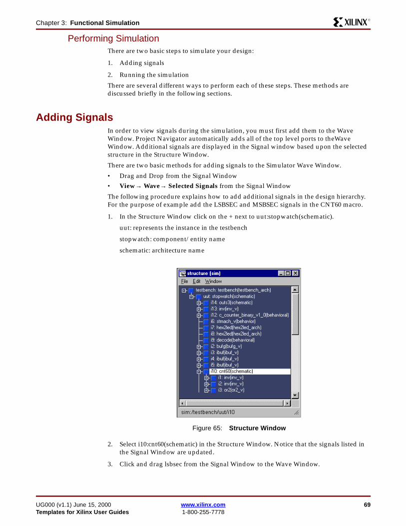
Chapter 3: Functional SimulationR
Performing SimulationThere are two basic steps to simulate your design:
1. Adding signals
2. Running the simulation
There are several different ways to perform each of these steps. These methods are discussed briefly in the following sections.
Adding SignalsIn order to view signals during the simulation, you must first add them to the Wave Window. Project Navigator automatically adds all of the top level ports to theWave Window. Additional signals are displayed in the Signal window based upon the selected structure in the Structure Window.
There are two basic methods for adding signals to the Simulator Wave Window.
• Drag and Drop from the Signal Window
• View→ Wave→ Selected Signals from the Signal Window
The following procedure explains how to add additional signals in the design hierarchy. For the purpose of example add the LSBSEC and MSBSEC signals in the CNT60 macro.
1. In the Structure Window click on the + next to uut:stopwatch(schematic).
uut: represents the instance in the testbench
stopwatch: component/entity name
schematic: architecture name
2. Select i10:cnt60(schematic) in the Structure Window. Notice that the signals listed in the Signal Window are updated.
3. Click and drag lsbsec from the Signal Window to the Wave Window.
Figure 65: Structure Window
UG000 (v1.1) June 15, 2000 www.xilinx.com 69Templates for Xilinx User Guides 1-800-255-7778
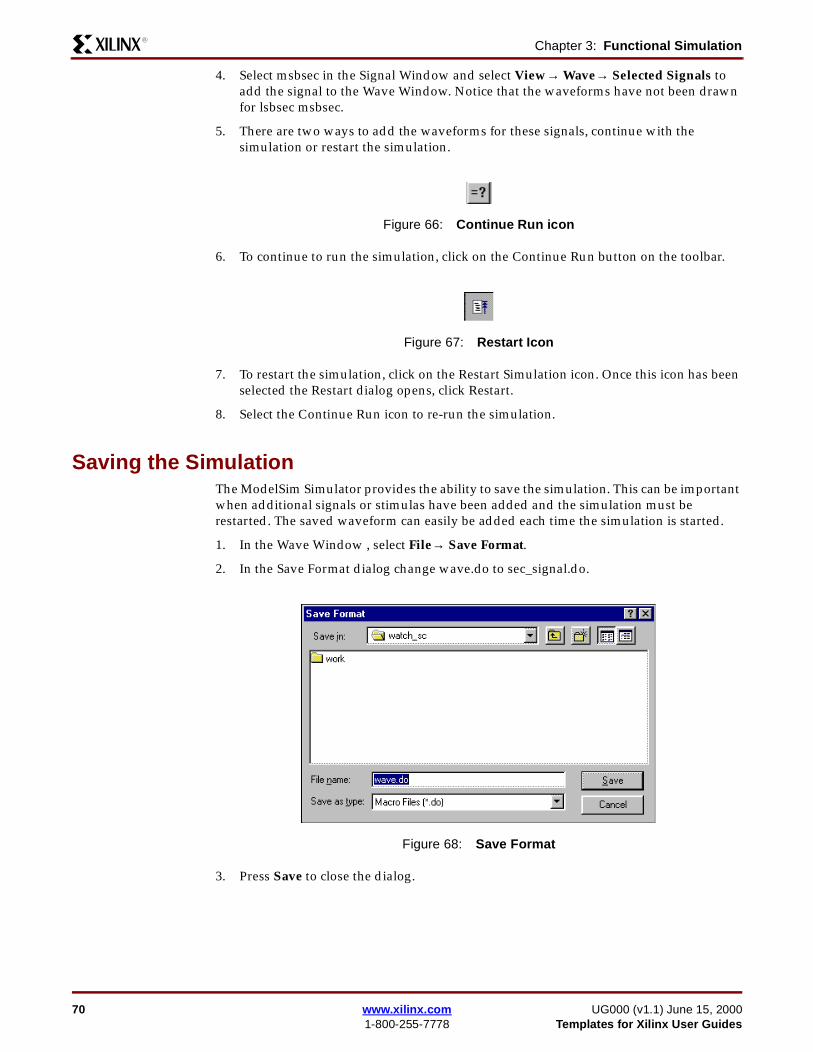
Chapter 3: Functional SimulationR
4. Select msbsec in the Signal Window and select View→ Wave→ Selected Signals to add the signal to the Wave Window. Notice that the waveforms have not been drawn for lsbsec msbsec.
5. There are two ways to add the waveforms for these signals, continue with the simulation or restart the simulation.
6. To continue to run the simulation, click on the Continue Run button on the toolbar.
7. To restart the simulation, click on the Restart Simulation icon. Once this icon has been selected the Restart dialog opens, click Restart.
8. Select the Continue Run icon to re-run the simulation.
Saving the SimulationThe ModelSim Simulator provides the ability to save the simulation. This can be important when additional signals or stimulas have been added and the simulation must be restarted. The saved waveform can easily be added each time the simulation is started.
1. In the Wave Window , select File→ Save Format.
2. In the Save Format dialog change wave.do to sec_signal.do.
3. Press Save to close the dialog.
Figure 66: Continue Run icon
Figure 67: Restart Icon
Figure 68: Save Format
70 www.xilinx.com UG000 (v1.1) June 15, 20001-800-255-7778 Templates for Xilinx User Guides

Chapter 3: Functional SimulationR
Restarting the SimulationIf you remember the original simulation resulted in errors between the expected and actual response of the simulation. These errors are the result of the reset signal being held high to long. Close the simulator by selecting File→ Quit in the ModelSim window.
These errors can easily be fixed by changing the stimulas in HDL Bencher. Open HDL Bencher by double clicking on stopwatch_tb.tbw in the Source Window of Project Navigator. This will open HDL Bencher.
The following procedure explains how to make the changes and restart the simulation.
1. In HDL Bencher click the reset cell below clk cycle 4 to set it low.
2. Save the waveform.
3. Export the test bench.
4. Close HDL Bencher.
5. VHDL Only. When HDL Bencher exported the new test bench the configuration information was lost. Add the configuration informatio to the test bench. Refer to the Adding the Test Bench to the Project section for more information.
6. Save the Test Bench and exit HDL Bencher.
7. To restart the simulation double click on the Simulate Functional VHDL or Verilog Model.
8. The Simulation will now complete without errors.
Figure 69: TBW file in Source Window
UG000 (v1.1) June 15, 2000 www.xilinx.com 71Templates for Xilinx User Guides 1-800-255-7778

Chapter 3: Functional SimulationR
72 www.xilinx.com UG000 (v1.1) June 15, 20001-800-255-7778 Templates for Xilinx User Guides

R
Chapter 4
Design Implementation
Design Implementation is the process of translating, mapping, placing, routing, and generating a BIT file for your design. The Design Implementation tools are embedded into the Foundation ISE Project Navigator for easy access and project management.
This chapter contains the following sections.
• “Project Management”• “Starting Implementation”
• “Running Implementation”• “Viewing Implementation Results”
• “Other Implementation Tools”
Project ManagementA Foundation ISE Project is maintained in a flat directory structure. The result of a flat directory structure is each time synthesis, simulation, or implementation is run, existing files are overwritten and/or new files are created.
A snapshot is a source of revision control. At any time in the design cycle the user can take a snapshot. A snapshot consists of all files in the current working directory. This includes synthesis and simulation sub-directories. To take a snapshot select Project→ Take Snapshot.
The take a Snapshot of the Project dialog provides a way for the user to enter the snapshot name and comments.
In the Snapshot View tab of the Source Window, all of the snapshots associated with the open project are displayed. To open a snapshot right click on the selected snapshot and select Open. This allows the user to view the project status, reports, user documents, and source files. All information displayed in the snapshot view is read-only.
A snapshot can also be restored to resume work at that phase in the design cycle. Select Project → Replace with Snapshot the snapshot is then restored as the current project and work can continue.
Figure 70: Take a Snapshot of the Project dialog
UG000 (v1.1) June 15, 2000 www.xilinx.com 73Templates for Xilinx User Guides 1-800-255-7778
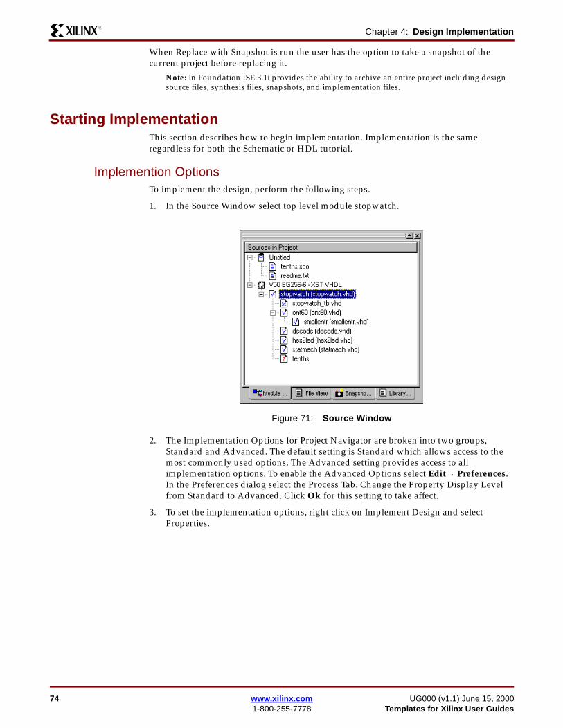
Chapter 4: Design ImplementationR
When Replace with Snapshot is run the user has the option to take a snapshot of the current project before replacing it.
Note: In Foundation ISE 3.1i provides the ability to archive an entire project including design source files, synthesis files, snapshots, and implementation files.
Starting ImplementationThis section describes how to begin implementation. Implementation is the same regardless for both the Schematic or HDL tutorial.
Implemention OptionsTo implement the design, perform the following steps.
1. In the Source Window select top level module stopwatch.
2. The Implementation Options for Project Navigator are broken into two groups, Standard and Advanced. The default setting is Standard which allows access to the most commonly used options. The Advanced setting provides access to all implementation options. To enable the Advanced Options select Edit→ Preferences. In the Preferences dialog select the Process Tab. Change the Property Display Level from Standard to Advanced. Click Ok for this setting to take affect.
3. To set the implementation options, right click on Implement Design and select Properties.
Figure 71: Source Window
74 www.xilinx.com UG000 (v1.1) June 15, 20001-800-255-7778 Templates for Xilinx User Guides
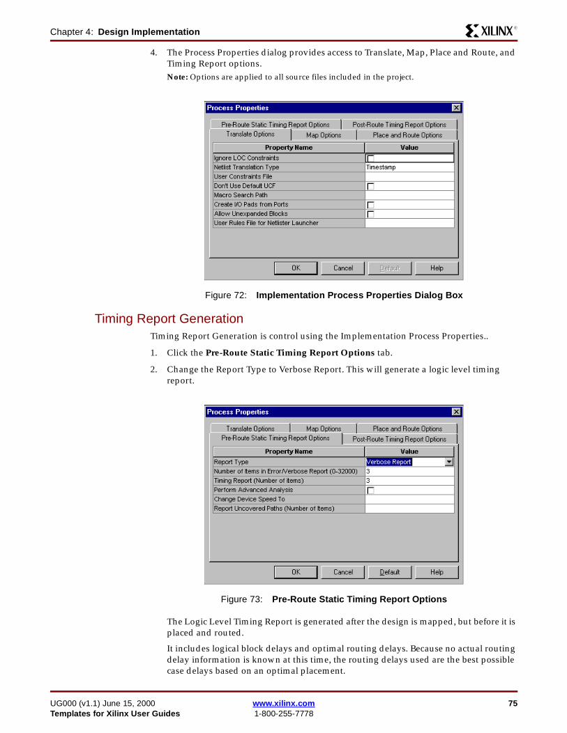
Chapter 4: Design ImplementationR
4. The Process Properties dialog provides access to Translate, Map, Place and Route, and Timing Report options.Note: Options are applied to all source files included in the project.
Timing Report GenerationTiming Report Generation is control using the Implementation Process Properties..
1. Click the Pre-Route Static Timing Report Options tab.
2. Change the Report Type to Verbose Report. This will generate a logic level timing report.
The Logic Level Timing Report is generated after the design is mapped, but before it is placed and routed.
It includes logical block delays and optimal routing delays. Because no actual routing delay information is known at this time, the routing delays used are the best possible case delays based on an optimal placement.
Figure 72: Implementation Process Properties Dialog Box
Figure 73: Pre-Route Static Timing Report Options
UG000 (v1.1) June 15, 2000 www.xilinx.com 75Templates for Xilinx User Guides 1-800-255-7778

Chapter 4: Design ImplementationR
The Post Layout Timing Report is generated after the design has been placed and routed and includes all of the routing delays for the design.
These reports are examined later.
3. If you want, examine the options available in the other tabs. For complete documentation on these options, refer to the online help or Foundation ISE User Guide.
4. Click OK.
Control FilesBy default, Project Navigator creates a blank UCF file in the project directory. You can edit this UCF file using the Constraints Editor or a text editor. Both of these processes are listed under Design Entry Utilities -- User Constraints.
Because the name of this UCF file is the same as the top level module, it is loaded by default. If you have other UCF files that you want to use instead, browse to find and select them.
You can also designate guide files or Floorplanner files to control the current implementation. For details, refer to the “Map and Place and route Options” section in the “FPGA Implementation Options” of Foundation Series ISE 3.1i User Guide.
Running ImplementationAfter setting the implementation options that you want, you are ready to implement the design.
1. Double Click the Implement Design process in the Process Window.
The Implementation Flow and Status are represented graphically in the Process Window, and a log of the processes is shown in the console at the bottom of the Project Navigator. Click on the “+” next to Implement Design to display all associated
76 www.xilinx.com UG000 (v1.1) June 15, 20001-800-255-7778 Templates for Xilinx User Guides
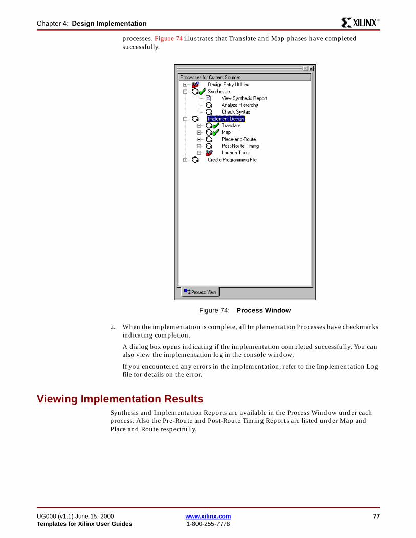
Chapter 4: Design ImplementationR
processes. Figure 74 illustrates that Translate and Map phases have completed successfully.
2. When the implementation is complete, all Implementation Processes have checkmarks indicating completion.
A dialog box opens indicating if the implementation completed successfully. You can also view the implementation log in the console window.
If you encountered any errors in the implementation, refer to the Implementation Log file for details on the error.
Viewing Implementation ResultsSynthesis and Implementation Reports are available in the Process Window under each process. Also the Pre-Route and Post-Route Timing Reports are listed under Map and Place and Route respectfully.
Figure 74: Process Window
UG000 (v1.1) June 15, 2000 www.xilinx.com 77Templates for Xilinx User Guides 1-800-255-7778

Chapter 4: Design ImplementationR
1. Expand the Map Process by selecting the “+”. The Map Report as well as the Pre-Route Static Timing Report are available.
2. Expand the Pre-Route Static Timing Process and double click on the Report to generate and open the Timing Report. Inspect this report to find the maximum system frequency specified. Remember this frequency. Close the report
3. Expand the Post-Route Process and double click on the Post-Route Timing Report. Inspect this report to find what the maximum frequency is. Compare this with the delay you found in the Logic Level Timing Report.
The difference in the two reports’ delays can be accounted for by the actual routing delays. The routing delays which are assumed in the Logic Level Timing Report are best-case, which is why they are generally smaller than the actual delays after placement and routing. Logic Level timing is useful because it gives you a preliminary look at how realistic your timing goals are, given the design’s current mapped state.
A rough guideline (known as the 50/50 rule) is that the logical block delays in any particular path will make up about 50% of the total path delay once the design is routed. This is, of course, just a guideline, and designs vary from case to case. But, this gives you some estimate to determine whether the design’s timing is even close to your goals before the design is completely placed and routed.
4. After you have perused the timing reports, close the reports and close the Report Browser.
Other Implementation ToolsThe Foundation ISE Project Navigator also gives you access to the other implementation tools, including the Timing Analyzer, FPGA Editor, Floorplanner, JTAG Programmer, Prom File Formatter and Hardware Debugger. These tools can be invoked from the Process Window under the Launch Tools and Create Programming File processes.
These implementation tools are sensitive to the current implementation. In other words, Project Navigator incorporates auto-make technology. Therefore if the design has not been implemented and you double click on FPGA Editor, Project Navigator will impelement the design and load FPGA Editor.
Now you can invoke any of these tools to see what they look like. For more information on using these tools, refer to the appropriate online documentation for each tool.
Figure 75: Expanded Map Process
78 www.xilinx.com UG000 (v1.1) June 15, 20001-800-255-7778 Templates for Xilinx User Guides
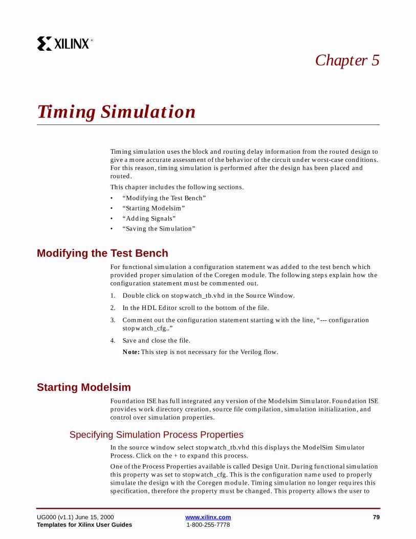
R
Chapter 5
Timing Simulation
Timing simulation uses the block and routing delay information from the routed design to give a more accurate assessment of the behavior of the circuit under worst-case conditions. For this reason, timing simulation is performed after the design has been placed and routed.
This chapter includes the following sections.
• “Modifying the Test Bench”• “Starting Modelsim”
• “Adding Signals”• “Saving the Simulation”
Modifying the Test BenchFor functional simulation a configuration statement was added to the test bench which provided proper simulation of the Coregen module. The following steps explain how the configuration statement must be commented out.
1. Double click on stopwatch_tb.vhd in the Source Window.
2. In the HDL Editor scroll to the bottom of the file.
3. Comment out the configuration statement starting with the line, “--- configuration stopwatch_cfg..”
4. Save and close the file.
Note: This step is not necessary for the Verilog flow.
Starting ModelsimFoundation ISE has full integrated any version of the Modelsim Simulator. Foundation ISE provides work directory creation, source file compilation, simulation initialization, and control over simulation properties.
Specifying Simulation Process PropertiesIn the source window select stopwatch_tb.vhd this displays the ModelSim Simulator Process. Click on the + to expand this process.
One of the Process Properties available is called Design Unit. During functional simulation this property was set to stopwatch_cfg. This is the configuration name used to properly simulate the design with the Coregen module. Timing simulation no longer requires this specification, therefore the property must be changed. This property allows the user to
UG000 (v1.1) June 15, 2000 www.xilinx.com 79Templates for Xilinx User Guides 1-800-255-7778
Chapter 5: Timing SimulationR
specify the top level model to be loaded in ModelSim. This property must be changed if the top level entity, configuration, or module is named something different than testbench.
For timing simulation the property must be changed to testbench. The following steps illustrate how to make this change:
1. Right click on Simulate Post-Route VHDL Model.
2. Select Properties...
3. Select the VHDL Post-Route Simulation Options tab.
4. Enter the following:
Design Unit Name: testbench
5. Click Ok to set the property.
Once the process properties have been set Modelsim can be invoked. To start the functional double click on Simulation Functional VHDL or Verilog Simulation.
ModelSim will now create the work directory, compile the source files, and initialize the simulation. By default the modelsim, wave, structure, and signal windows are opened. This can be modified in the process properties.
Once the simulation has run for the specified time, ModelSim will report several failures because the expected response does not match the actual response. These failures will be addressed later in the tutorial.
Performing SimulationThere are two basic steps to simulate your design:
1. Adding signals
2. Running the simulation
Figure 76: Properties
80 www.xilinx.com UG000 (v1.1) June 15, 20001-800-255-7778 Templates for Xilinx User Guides
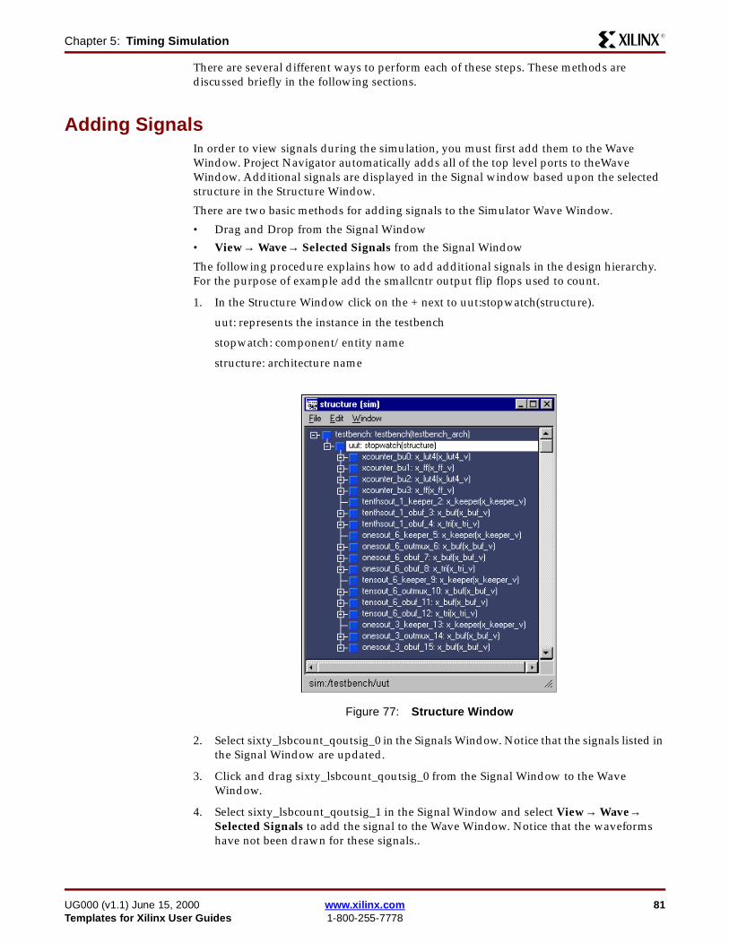
Chapter 5: Timing SimulationR
There are several different ways to perform each of these steps. These methods are discussed briefly in the following sections.
Adding SignalsIn order to view signals during the simulation, you must first add them to the Wave Window. Project Navigator automatically adds all of the top level ports to theWave Window. Additional signals are displayed in the Signal window based upon the selected structure in the Structure Window.
There are two basic methods for adding signals to the Simulator Wave Window.
• Drag and Drop from the Signal Window
• View→ Wave→ Selected Signals from the Signal Window
The following procedure explains how to add additional signals in the design hierarchy. For the purpose of example add the smallcntr output flip flops used to count.
1. In the Structure Window click on the + next to uut:stopwatch(structure).
uut: represents the instance in the testbench
stopwatch: component/entity name
structure: architecture name
2. Select sixty_lsbcount_qoutsig_0 in the Signals Window. Notice that the signals listed in the Signal Window are updated.
3. Click and drag sixty_lsbcount_qoutsig_0 from the Signal Window to the Wave Window.
4. Select sixty_lsbcount_qoutsig_1 in the Signal Window and select View→ Wave→ Selected Signals to add the signal to the Wave Window. Notice that the waveforms have not been drawn for these signals..
Figure 77: Structure Window
UG000 (v1.1) June 15, 2000 www.xilinx.com 81Templates for Xilinx User Guides 1-800-255-7778

Chapter 5: Timing SimulationR
5. There are two ways to add the waveforms for these signals, continue with the simulation or restart the simulation.
6. To continue to run the simulation, click on the Continue Run button on the toolbar.
7. To restart the simulation, click on the Restart Simulation icon. Once this icon has been selected the Restart dialog opens, click Restart.
8. Select the Continue Run icon to re-run the simulation.
Saving the SimulationThe ModelSim Simulator provides the ability to save the simulation. This can be important when additional signals or stimulas have been added and the simulation must be restarted. The saved waveform can easily be added each time the simulation is started.
1. In the Wave Window , select File→ Save Format.
2. In the Save Format dialog change wave.do to sec_signal.do.
3. Press Save to close the dialog.
4. Close the Simulator.
Figure 78: Continue Run icon
Figure 79: Restart Icon
Figure 80: Save Format
82 www.xilinx.com UG000 (v1.1) June 15, 20001-800-255-7778 Templates for Xilinx User Guides