
Forward modeling method for microstructure reconstruction using x ...
12
Forward modeling method for microstructure reconstruction using x-ray diffraction microscopy: Single-crystal verification R. M. Suter Department of Physics and Department of Materials Science and Engineering, Carnegie Mellon University, Pittsburgh, Pennsylvania 15213 D. Hennessy and C. Xiao Department of Physics, Carnegie Mellon University, Pittsburgh, Pennsylvania 15213 U. Lienert Advanced Photon Source, Argonne National Laboratory, Argonne, Illinois 60439 Received 22 August 2006; accepted 23 October 2006; published online 20 December 2006 We describe and illustrate a forward modeling method for quantitatively reconstructing the geometry and orientation of microstructural features inside of bulk samples from high-energy x-ray diffraction microscopy data. Data sets comprise charge-coupled device images of Bragg diffracted beams originating from individual grains in a thin planar section of sample. Our analysis approach first reduces the raw images to a binary data set in which peaks have been thresholded at a fraction of their height after noise reduction processing. We then use a computer simulation of the measurement and the sample microstructure to generate calculated diffraction patterns over the same range of sample orientations used in the experiment. The crystallographic orientation at each of an array of area elements in the sample space is adjusted to optimize overlap between experimental and simulated scattering. In the present verification exercise, data are collected at the Advanced Photon Source beamline 1-ID using microfocused 50 keV x rays. Our sample is a thin silicon wafer. By choosing the appropriate threshold fraction and convergence criteria, we are able to reconstruct to 10 m errors the subregion of the silicon wafer that remains in the incident beam throughout the rotation range of the measurement. The standard deviation of area element orientations is 0.3°. Our forward modeling approach offers a degree of noise immunity, is applicable to polycrystals and composite materials, and can be extended to include scattering rules appropriate for defected materials. © 2006 American Institute of Physics. DOI: 10.1063/1.2400017 I. INTRODUCTION X-ray diffraction microscopy 1,2 constitutes a set of tech- niques that can be used to probe the microstructure deep inside of bulk materials. Because the measurements are non- destructive, they give access to the dynamic response of en- sembles of grains to stimuli such as heat, stress, or chemistry. Using focused beams of high-energy photons with E 40 keV that penetrate millimeters to centimeters of mate- rials, these techniques can spatially resolve local crystallo- graphic orientation, grain shapes, and strain states. While high-energy x rays are available at a number synchrotron beam lines around the world, the undulator radiation from third generation sources has the spectral range, brilliance, and source size most desirable for the experimental require- ments. At present, there is an apparatus at ID-11 at the Eu- ropean Synchrotron Radiation Facility ESRF that is dedi- cated to such measurements 1 and, as illustrated here, a similar capability is being developed at the Advanced Photon Source. Studies to date have probed, for example, in situ response to stress, 3,4 internal grain growth in real time, 5,6 and observation of phase transformations. 7 In this paper, we are concerned with the problem of re- constructing the location and shape of ensembles of grains in three dimensions. This is done by isolating and imaging dif- fracted beams originating from individual grains and track- ing their path through space in order to locate their position of origin. 8,9 The position and shape resolution are expected to reach 1 m while orientations can be measured to well below a degree. However, the reconstruction problem is for- midable even for ideal samples with sharp Bragg scattering and it is more so in the case of samples with a significant defect content. 1,9 We report here on a new approach involv- ing forward modeling or computer simulation and we dem- onstrate its application using a simple, single-crystal sample of silicon. It should be possible to generalize this approach to treat not only simple polycrystals but defected and composite materials as well. The development of a three-dimensional polycrystal mapping ability is timely. For example, recent work using electron probes 10,11 has provided new statistical measures of grain boundary character distributions in a variety of poly- crystals and has revealed that systematic anisotropic distri- butions emerge from simple thermal grain growth treatments. Volumetric measurements are now needed to understand, on a grain-by-grain basis, how these distributions arise, how they are affected by different starting conditions, and how they can be influenced by defect content, impurities, inclu- sions, and other factors. Recent three-dimensional grain REVIEW OF SCIENTIFIC INSTRUMENTS 77, 123905 2006 0034-6748/2006/7712/123905/12/$23.00 © 2006 American Institute of Physics 77, 123905-1 Downloaded 02 Jan 2007 to 128.2.116.133. Redistribution subject to AIP license or copyright, see http://rsi.aip.org/rsi/copyright.jsp
Transcript of Forward modeling method for microstructure reconstruction using x ...

Forward modeling method for microstructure reconstruction using x-raydiffraction microscopy: Single-crystal verification
R. M. SuterDepartment of Physics and Department of Materials Science and Engineering, Carnegie Mellon University,Pittsburgh, Pennsylvania 15213
D. Hennessy and C. XiaoDepartment of Physics, Carnegie Mellon University, Pittsburgh, Pennsylvania 15213
U. LienertAdvanced Photon Source, Argonne National Laboratory, Argonne, Illinois 60439
�Received 22 August 2006; accepted 23 October 2006; published online 20 December 2006�
We describe and illustrate a forward modeling method for quantitatively reconstructing thegeometry and orientation of microstructural features inside of bulk samples from high-energy x-raydiffraction microscopy data. Data sets comprise charge-coupled device images of Bragg diffractedbeams originating from individual grains in a thin planar section of sample. Our analysis approachfirst reduces the raw images to a binary data set in which peaks have been thresholded at a fractionof their height after noise reduction processing. We then use a computer simulation of themeasurement and the sample microstructure to generate calculated diffraction patterns over the samerange of sample orientations used in the experiment. The crystallographic orientation at each of anarray of area elements in the sample space is adjusted to optimize overlap between experimental andsimulated scattering. In the present verification exercise, data are collected at the Advanced PhotonSource beamline 1-ID using microfocused 50 keV x rays. Our sample is a thin silicon wafer. Bychoosing the appropriate threshold fraction and convergence criteria, we are able to reconstruct to�10 �m errors the subregion of the silicon wafer that remains in the incident beam throughout therotation range of the measurement. The standard deviation of area element orientations is �0.3°.Our forward modeling approach offers a degree of noise immunity, is applicable to polycrystals andcomposite materials, and can be extended to include scattering rules appropriate for defectedmaterials. © 2006 American Institute of Physics. �DOI: 10.1063/1.2400017�
I. INTRODUCTION
X-ray diffraction microscopy1,2 constitutes a set of tech-niques that can be used to probe the microstructure deepinside of bulk materials. Because the measurements are non-destructive, they give access to the dynamic response of en-sembles of grains to stimuli such as heat, stress, or chemistry.Using focused beams of high-energy photons with E�40 keV that penetrate millimeters to centimeters of mate-rials, these techniques can spatially resolve local crystallo-graphic orientation, grain shapes, and strain states. Whilehigh-energy x rays are available at a number synchrotronbeam lines around the world, the undulator radiation fromthird generation sources has the spectral range, brilliance,and source size most desirable for the experimental require-ments. At present, there is an apparatus at ID-11 at the Eu-ropean Synchrotron Radiation Facility �ESRF� that is dedi-cated to such measurements1 and, as illustrated here, asimilar capability is being developed at the Advanced PhotonSource. Studies to date have probed, for example, in situresponse to stress,3,4 internal grain growth in real time,5,6 andobservation of phase transformations.7
In this paper, we are concerned with the problem of re-constructing the location and shape of ensembles of grains inthree dimensions. This is done by isolating and imaging dif-
fracted beams originating from individual grains and track-ing their path through space in order to locate their positionof origin.8,9 The position and shape resolution are expectedto reach �1 �m while orientations can be measured to wellbelow a degree. However, the reconstruction problem is for-midable even for ideal samples with sharp Bragg scatteringand it is more so in the case of samples with a significantdefect content.1,9 We report here on a new approach involv-ing forward modeling or computer simulation and we dem-onstrate its application using a simple, single-crystal sampleof silicon. It should be possible to generalize this approach totreat not only simple polycrystals but defected and compositematerials as well.
The development of a three-dimensional polycrystalmapping ability is timely. For example, recent work usingelectron probes10,11 has provided new statistical measures ofgrain boundary character distributions in a variety of poly-crystals and has revealed that systematic anisotropic distri-butions emerge from simple thermal grain growth treatments.Volumetric measurements are now needed to understand, ona grain-by-grain basis, how these distributions arise, howthey are affected by different starting conditions, and howthey can be influenced by defect content, impurities, inclu-sions, and other factors. Recent three-dimensional grain
REVIEW OF SCIENTIFIC INSTRUMENTS 77, 123905 �2006�
0034-6748/2006/77�12�/123905/12/$23.00 © 2006 American Institute of Physics77, 123905-1
Downloaded 02 Jan 2007 to 128.2.116.133. Redistribution subject to AIP license or copyright, see http://rsi.aip.org/rsi/copyright.jsp

growth simulations12,13 using model driving forces appear toyield grain boundary character distributions that are statisti-cally similar to experimental measurements. Measurementsof the evolution of real materials can be used to test andconstrain the growth rules used in such simulations.
Figure 1 shows a schematic of the experimental geom-etry. This is configuration B as described by Poulsen, and weuse the same coordinate system conventions.1 A line focused,monochromatic beam of x rays illuminates a thin section��1 �m thick by �1 mm wide� of the sample that ismounted on a rotation stage, �, with the axis normal to theilluminated plane. A beam stop prevents the transmittedbeam from striking the downstream area detector. The highspatial resolution detector �for example, 4 �m pixels� imagesdiffracted beams emanating from crystallites that happen tosatisfy a Bragg condition at orientation �. The detector ispositioned close to the sample ��5−10 mm� so that the po-sition of a diffracted beam spot is sensitive to both the dif-fracted beam direction �specified by 2� and �� and the posi-tion of origin within the sample. This information is encodedin the data by measuring the diffraction pattern at a number,NL�3, of rotation axis-to-detector distances, L. In order toobserve as many diffracted beams as possible, continuouscoverage of the rotation � is needed. Detector images aretherefore collected while the sample is rotated through aninterval, ���1°, and N� adjacent intervals are measuredso as to cover a range ��=N��� large enough to ensureobservation of several Bragg peaks from grains of arbitraryorientation.
Another technique for nondestructive probing of internalmicrostructure is the polychromatic x-ray microbeammethod developed by Ice and Larson.14 This method, using aspot focused beam, has better �submicrometer� spatial reso-lution but has less penetration depth, making it appropriatefor thin and small grained structures. Recent work, for ex-
ample, has characterized deformation microstructures of in-dividual grains.15 Volumetric data collection requires roughlyan image per voxel whereas the current method collects datain transmission from planar sections through many grains inparallel.8
The next section gives a detailed account of our dataanalysis and map construction approach along with compari-sons to other approaches. This is followed by a description ofthe apparatus at the Advanced Photon Source and a verifica-tion exercise using the simplest possible microstructure: asingle crystal of silicon. Evaluation of the results, implica-tions for applications to polycrystal samples, and prospectsfor further development are discussed in Sec. IV.
II. ANALYSIS METHOD
Reconstruction of a three-dimensional microstructure re-quires the processing of thousands of detector images. Eachtwo dimensional slice requires 100–300 images and manyslices are required to extend into three dimensions. In a poly-crystal, each image may include 10–100 diffraction spotsoriginating from different regions of the illuminated samplespace. Since a primary purpose of the nondestructive mea-surement is to allow observation of the response of the mi-crostructure to external stimuli, many three-dimensionalmaps may be needed. It is clear that analysis of such datasets must be extensively automated.
We describe here an analysis method in which we simu-late or forward model the entire measurement process includ-ing the x-ray beam and detector, experimental geometry, andsample microstructure. The sample microstructure is de-scribed on a discretized grid representing the illuminatedplane of the sample with each area element having an asso-ciated phase, orientation, and, possibly, defect structure.Software can adjust parameters describing both the sampleand experiment to make the simulated diffraction match theobserved data as well as possible. As presently implemented,this is an ab initio approach that requires no initial crosscorrelation of the diffraction images and no prior knowledgeof orientations present in the sample. What is required is areasonably well-defined set of experimental parameters and aknown nominal crystal structure. This initial informationmust be sufficient that at least some regions in the samplecan be made to generate scattering that overlaps a minimalset of experimentally observed diffracted beams. With thisinitial success, experimental parameters can be refined, ascan the spatial resolution of the simulated or fitted micro-structure. One advantage of this approach is that the simula-tion can use and adjust realistic scattering physics appropri-ate for the sample under consideration. Lattice bending thatgives rise to a mosaic spread in the observed data can bemodeled directly in the crystal frame of reference. Also, de-tector point spread functions can be modeled so as to avoidthe complications of attempting to deconvolve observed datasets.
Our forward modeling approach is an alternative to sev-eral current analysis schemes1,7,8,14–21 includingGRAINDEX, GRAINSWEEPER, and the algebraic recon-struction technique �ART�. To put our work in context, we
FIG. 1. Schematic of the x-ray beam, sample, and detector. We use a singledetector and move it sequentially to the positions shown. Diffraction fromone particular grain is shown together with notation �2� and �� for specify-ing the direction of the diffracted wave vector, k f =kv, with k=2 /. Notethat a circular grain in the illuminated plane generates an elliptical spot onthe detector due to the projection along v. The coordinate system origin is atthe intersection of the rotation axis and the beam plane and the beam isincident in the x direction.
123905-2 Suter et al. Rev. Sci. Instrum. 77, 123905 �2006�
Downloaded 02 Jan 2007 to 128.2.116.133. Redistribution subject to AIP license or copyright, see http://rsi.aip.org/rsi/copyright.jsp

give a very brief comparison to other methods but refer thereader to the references for detailed descriptions. GRAIN-DEX is an indexing scheme that correlates observed diffrac-tion spots into groups that are crystallographically consistentso as to yield a list of grain orientations with center-of-masspositions in the illuminated sample plane. ART combines theset of intensity patterns corresponding to a given orientationand uses tomographic algorithms to reconstruct the grainshape. GRAINDEX and ART work primarily in the dataspace to deduce properties of diffracting entities in thesample; in this sense, they attempt to solve the inverse prob-lem. These approaches are quite sensitive to the overlap ofspots as diffracted beams from different sample regions crossat the detector position18 and to broadening effects due todefect scattering.
GRAINSWEEPER and our simulation approach analyzethe possible scattering from localized sample regions andsearch for optimum orientations over a gridded samplespace; these can be characterized as forward modeling ordata fitting procedures. GRAINSWEEPER identifies detectorregions where a primary Bragg peak type could appear andsearches for intensity therein. The detector region for a sec-ond peak, crystallographically consistent with the first, isthen searched. This constrained search is computationally ef-ficient but requires the specification of preferred Bragg peaktypes that must be in the observed data set for all grains. Ourapproach is less computationally efficient but treats a largenumber of peaks equally. We use Monte Carlo optimizationof orientations, which uses all the scattering generated by thesimulation and attempts to minimize a global cost function.An occasional overlap of spots does not limit convergence.Further, Monte Carlo variation of scattering parameters andexperimental geometry is trivial to implement �at least in itssimplest form�. As pointed out previously,1,9 combining anefficient initial computation with a Monte Carlo based finalstep is quite desirable. We have implemented this to the ex-tent that we first perform a search over a discrete orientationset before beginning the Monte Carlo optimization. Finally,other experimental configurations, such as use of a large or“box” beam,1 can be treated with a generalization of ourcurrent model. The flexibility of the simulation approachcombined with the availability of ever more computationalpower should allow simulations to play a significant role inthe analysis of x-ray diffraction microscope data.
A. Sample simulation
Approximating the incident x-ray beam as illuminating athin section of the experimental sample allows an analysis tobe done on a layer-by-layer basis. The planar section of themicrostructure is simulated as a mesh of area elements, eachwith independent parameters describing the local crystallo-graphic orientation, a switch, � , to indicate the type of scat-tering generated by the element, and other parameters de-scribing the state of convergence in the fitting process �Sec.II D�. A list of Bragg peaks that are candidates for beinggenerated by each area element is specified. The area cov-ered by the mesh may be smaller or larger than the actualsample being measured. � can be a binary indicator of thepresence or absence of scattering from the element or, more
generally, can take on different values to indicate the pres-ence of a particular crystallographic phase as appropriate formeasurements of composite materials.
In our implementation, the sample mesh is a triangulargrid of area elements �Fig. 2�. The initial mesh can be adap-tively refined by dividing selected parent triangles into foursmaller ones with the offspring having the same properties asthe parents. The fitting procedures can then determine opti-mized parameters so as to better define boundaries where, forexample, orientations change rapidly. Crystallographic orien-tation g �specified in the sample reference frame� is relativeto unit cells being aligned with the laboratory axes of Fig. 1when �=0. The list of reciprocal lattice vectors, Ghkl, isgenerated from elementary specification of unit cell dimen-sions, basis atom positions, and atomic form factors �ap-proximated in the small scattering vector limit�. A maximumGhkl �i.e., 2�� can be specified and peaks with intensitiesgreater than a specified fraction of the maximum intensityare put into the list of candidates. This approach makes itstraightforward to model any type of crystal, from elementalto complex molecular.22
B. Scattering calculations
For a given set of parameters, �g ,��, an area elementwill generate Bragg scattering in several different � inter-vals. The simulation needs to determine which candidatepeaks are generated in experimentally measured intervalsand, of these, which diffracted beams actually hit the detec-tors at each position, L. The geometry of the area element isthen projected onto the relevant detectors to determine thedetector pixels that are illuminated. In the fitting process, wethen ask whether the corresponding experimental pixels areilluminated. The detector space is four dimensional and canbe parametrized as D�j ,k , iL , i��, where j and k are pixelindices, iL picks one of the detector distances �Fig. 1�, and i�
specifies the � interval in which the Bragg peak falls.
FIG. 2. Schematic diagram of the simulation geometry. The sample is rep-resented by a hexagonal grid with each element assigned its own crystallo-graphic phase and orientation, �� j , g j�. For elements that generate scatteringat this � �dark triangles�, the grid element vertices are projected along a unitvector, v, parallel to the scattered wave vector, k f, onto the detector �blackdots in magnified view at right�. Any detector pixel inside or intersected bythe projected triangle is considered to be illuminated by this Bragg peak�filled squares�.
123905-3 X-ray diffraction microscopy Rev. Sci. Instrum. 77, 123905 �2006�
Downloaded 02 Jan 2007 to 128.2.116.133. Redistribution subject to AIP license or copyright, see http://rsi.aip.org/rsi/copyright.jsp

In the simplest case, the Bragg condition is evaluatedand scattering is assumed to be sharp, i.e., a � function at
Q � k f − ki = Ghkl, �1�
with k f and ki being the final and incident wave vectors.However, many generalizations are possible and desirable:the incident beam may not be perfectly monochromatic orparallel, and the crystal structure may be distorted by homo-geneous strain or local defect content. If the consequent mo-tion and/or broadening of Bragg scattering can be param-etrized, then these effects can be included here and adjustedby fitting procedures.
For a particular Ghkl �specified in conventional crystalnotation� the Bragg condition �1� in the laboratory frame ofreference determines � and � �the scattering angle 2� beingalready defined by Ghkl=2k sin ��:
�Ghkllab�x = −
�Ghkl�2
2k, �2�
where the incident wave vector is ki=kx and Ghkllab
=�−1���U−1�g�Ghkl. Here, U−1�g� is the matrix giving thecrystal lattice orientation relative to the sample coordinatesand ���� is the matrix corresponding to rotation by � aboutthe z axis. Equation �2� yields either zero or two Bragg val-ues, �B. If U−1�g�Ghkl lies too close to the rotation axis, thecomponent in the xy plane will be too small to ever satisfy�2�; the condition for a solution is that ��B, where is theangle between the z axis and U−1�g�Ghkl and �B is the Braggangle. At high energies, many Bragg angles are small, so alarge region of reciprocal space is covered by the single �rotation in combination with an area detector. For ��B,there are two solutions to �2� having the in-plane projectionof U−1�g�Ghkl
lab on either side of the incident beam.Once a relevant Bragg condition has been determined,
the simulated detector image is updated. The triangle verticesare moved to laboratory coordinates with �−1���. The areaelement is then projected along k f =kv onto the detectors forthe appropriate � and L and the detector images are updatedfollowing the procedure outlined in Fig. 2.
We have incorporated a number of correction parametersto mimic possible experimental realities. Misalignment ofthe detector translation is included by specifying the detectororigin, �j0 ,k0�, separately at each detector distance, L. Rota-tion stage �x ,y� offsets can be entered for each � interval.Detector plane misorientation is specified by rotations aboutthe laboratory axes. The finite incident x-ray beam height isincorporated by summing contributions from different zelevations.
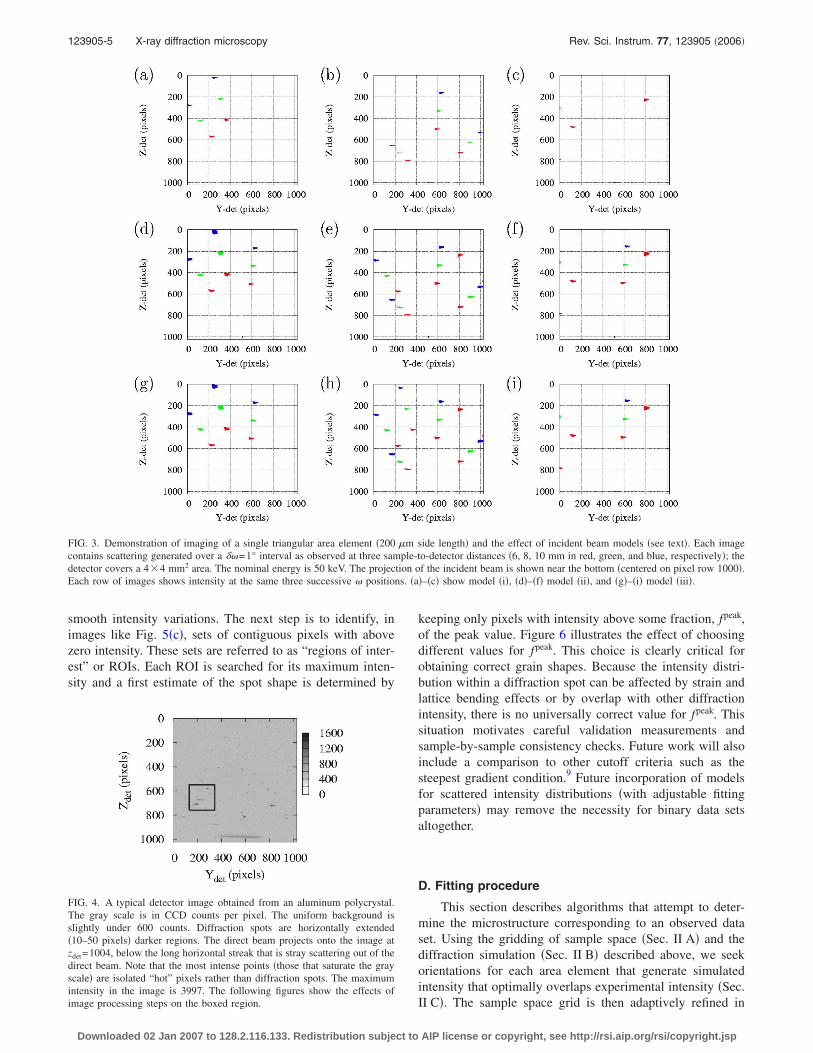
Finally, here we illustrate broadening effects due to in-cident beam properties. These properties are governed by themonochromator and focusing optics and can significantly af-fect observed scattering under realistic conditions. The ef-fects illustrated here can be difficult to handle in data inver-sion approaches to analysis. We model the finite energybandwidth, �E, and variations in the angle of incidence rela-tive to the nominal beam plane, � , by summing a set ofdiscrete contributions. Figure 3 compares three incidentbeam models: �i� �E=� =0 �ideal case�, �ii� �E /E=0.02,with � =0, and �iii� �E /E=0.02 with � �0.1° with be-
ing correlated with E in a manner appropriate for a bentsilicon �111� Laue monochromator crystal.23,24 �E /E is cho-sen as 2% in order to make effects visible in the images.Model �i� yields triangular diffraction spots that are projec-tions, at the appropriate �, of the triangular sample area el-ement. The higher order spots are more extended in the zdirection due to the larger projection angle. The broadenedspots of model �ii� are the result of different diffractionangles for the different energy contributions. Spots progres-sively broaden as the sample-to-detector distance increases.The more obvious effect is that some peaks cross over todifferent � intervals as the energy varies: the high order peaknear the center of �b� is spread over all three images �d�–�f�.The split spots appear rather sharp in �d� and �f�, indicatingthat only a narrow part of the bandwidth contributes here.Other such split peaks can also be identified by comparisonwith �a�–�c�. For model �iii�, not surprisingly, additionalbroadening and crossings of � intervals occurs.
C. Raw data and image analysis
The raw experimental data is in the form of images ofdiffraction patterns observed with a two-dimensional x-raydetector. Detector hardware and characterization are dis-cussed in Sec. III A. Here, we describe the process of takingraw charge-coupled device �CCD� based images and gener-ating a binary reduced data set that yields geometrical infor-mation about the diffracting entities in the sample. In otherwords, from the continuous intensity distributions in ob-served diffraction spots, we attempt to deduce shapes on thedetector that correspond to projections of the shapes of indi-vidual crystalline grains. Because the reconstructed orienta-tion of each area element in the sample depends on matchingits diffraction to many Bragg spots, some random errors indeduced shapes can be tolerated. However, in the averagedsense, accurate shapes are critical.
Due to the combination of data collection time con-straints and the inefficiency of the detector system �Sec.III A�, signal levels can be quite low, and this complicatesthe above process. Figure 4 shows a typical diffraction pat-tern obtained from an aluminum polycrystal. Even with bet-ter statistics on low-order Bragg peaks, we expect to have todeal with weak signals in higher-order peaks. Because oftheir larger scattering angle, these peaks tend to have betterprojection geometries than low-order peaks, so deducingtheir shapes accurately can yield improved spatial resolutionin the reconstruction. Thus, image processing is a critical andchallenging aspect of the reconstruction process.
The image reduction process is illustrated in Figs. 5 and6, which show a subregion of the image in Fig. 4. The uni-form background in Fig. 4 or Fig. 5�a� is due to dark currentin the CCD. Simple background subtraction yields improvedcontrast but leaves many isolated “hot” pixels. These anoma-lous points must be removed in order to allow consistentintensity estimates within the diffraction spots. Figure 5�c�demonstrates that this can be done using a median filter. Thefilter passes a 3�3 pixel mask over the image and replacesthe center pixel intensity with the median of values withinthe mask. This nonlinear process has the effect of removingisolated high �or low� pixels without strongly affecting
123905-4 Suter et al. Rev. Sci. Instrum. 77, 123905 �2006�
Downloaded 02 Jan 2007 to 128.2.116.133. Redistribution subject to AIP license or copyright, see http://rsi.aip.org/rsi/copyright.jsp
smooth intensity variations. The next step is to identify, inimages like Fig. 5�c�, sets of contiguous pixels with abovezero intensity. These sets are referred to as “regions of inter-est” or ROIs. Each ROI is searched for its maximum inten-sity and a first estimate of the spot shape is determined by
keeping only pixels with intensity above some fraction, fpeak,of the peak value. Figure 6 illustrates the effect of choosingdifferent values for fpeak. This choice is clearly critical forobtaining correct grain shapes. Because the intensity distri-bution within a diffraction spot can be affected by strain andlattice bending effects or by overlap with other diffractionintensity, there is no universally correct value for fpeak. Thissituation motivates careful validation measurements andsample-by-sample consistency checks. Future work will alsoinclude a comparison to other cutoff criteria such as thesteepest gradient condition.9 Future incorporation of modelsfor scattered intensity distributions �with adjustable fittingparameters� may remove the necessity for binary data setsaltogether.
D. Fitting procedure
This section describes algorithms that attempt to deter-mine the microstructure corresponding to an observed dataset. Using the gridding of sample space �Sec. II A� and thediffraction simulation �Sec. II B� described above, we seekorientations for each area element that generate simulatedintensity that optimally overlaps experimental intensity �Sec.II C�. The sample space grid is then adaptively refined in
FIG. 3. Demonstration of imaging of a single triangular area element �200 �m side length� and the effect of incident beam models �see text�. Each imagecontains scattering generated over a ��=1° interval as observed at three sample-to-detector distances �6, 8, 10 mm in red, green, and blue, respectively�; thedetector covers a 4�4 mm2 area. The nominal energy is 50 keV. The projection of the incident beam is shown near the bottom �centered on pixel row 1000�.Each row of images shows intensity at the same three successive � positions. �a�–�c� show model �i�, �d�–�f� model �ii�, and �g�–�i� model �iii�.
FIG. 4. A typical detector image obtained from an aluminum polycrystal.The gray scale is in CCD counts per pixel. The uniform background isslightly under 600 counts. Diffraction spots are horizontally extended�10–50 pixels� darker regions. The direct beam projects onto the image atzdet=1004, below the long horizontal streak that is stray scattering out of thedirect beam. Note that the most intense points �those that saturate the grayscale� are isolated “hot” pixels rather than diffraction spots. The maximumintensity in the image is 3997. The following figures show the effects ofimage processing steps on the boxed region.
123905-5 X-ray diffraction microscopy Rev. Sci. Instrum. 77, 123905 �2006�
Downloaded 02 Jan 2007 to 128.2.116.133. Redistribution subject to AIP license or copyright, see http://rsi.aip.org/rsi/copyright.jsp

order to better resolve regions where properties changerapidly.
Data, both experimental and simulated, are stored in anarray, D�j ,k , iL , i��, as defined in Sec. II B. The low-order bitholds the reduced experimental data while higher-order bitsstore simulated intensity. Of order 300 mega-bytes is re-quired for a single layer. Typically, less than 1% of detectorpixels are included in the reduced experimental data set anda comparable number of pixels are struck by the simulation.
As the orientation associated with a particular samplearea element is varied, a given Bragg peak, with scatteringangle, 2�, sweeps through � and � �Fig. 1�. For some orien-tations, it disappears out of the experimentally accessed sub-space of these variables. As it moves, this simulated peakmay accidentally overlap experimental intensity comingfrom another part of the sample but it is unlikely to do so atall measured detector positions, L, at the relevant �. Only fora very restricted range of orientations �for the given area
element� will multiple simulated peaks overlap experimentalspots at multiple L’s. This sort of overlap is the goal of theorientation search. Below, an acceptance criterion, Fmin, isdeveloped that measures the level of this success.
1. Fmin acceptance criterionA hierarchy of procedures is necessary to determine if an
orientation qualifies as a valid fit for an area element. At eachorientation, g, we calculate the fraction, F�g�, of qualifyingsimulated Bragg peaks �see below� that overlap experimen-tally observed intensity. The basic question is, does a suffi-cient fraction, Fmin, of qualifying simulated Bragg peaksoverlap experimentally observed intensity? Determination ofF�g� involves the following considerations:
1. A “qualifying simulated Bragg peak” is one that strikesthe detector at least at the two smallest measured L po-sitions �unless only a single L was measured�.
2. For a simulated Bragg peak to be said to overlap experi-mentally observed intensity in a given detector image, itmust satisfy fhit�nexp/Nsim� fmin
hit . As illustrated in Fig.7, Nsim is the number of detector pixels covered by theprojection of the sample area element onto the detector�Fig. 2� while nexp is the number of those pixels that arealso illuminated in the experiment. fmin
hit is an acceptancecriterion typically set to 0.5.
3. For a qualifying simulated peak to be said to overlapexperimental intensity, it must satisfy the criterion initem 2 at every detector position �at the relevant �� withL�Lmax
sim , where Lmaxsim is the maximum measured distance
at which the simulated peak is on the detector. For ex-ample, if the scattering shown in Fig. 1 is generated bythe simulation and it hits the detector at all three posi-tions as shown, then it must overlap experimental inten-sity at all three detector positions to qualify as overlap-
FIG. 5. Expanded view of the subregion indicated in Fig. 4 in three stages ofimage analysis. �a� Raw image �gray scale 0–1600; this scale saturates somepixels since the maximum in the figure is 2700�, �b� background �600counts� subtracted image �gray scale 0–1000�, and �c� median filtered andbackground subtracted image �gray scale 0–1000�.
FIG. 6. Binary images of data from Fig. 5. Each region of interest has beenthresholded at a fraction of the maximum intensity in the region. Thresholdsare �a� fpeak=0.5 and �b� 0.25 of the peak height.
123905-6 Suter et al. Rev. Sci. Instrum. 77, 123905 �2006�
Downloaded 02 Jan 2007 to 128.2.116.133. Redistribution subject to AIP license or copyright, see http://rsi.aip.org/rsi/copyright.jsp
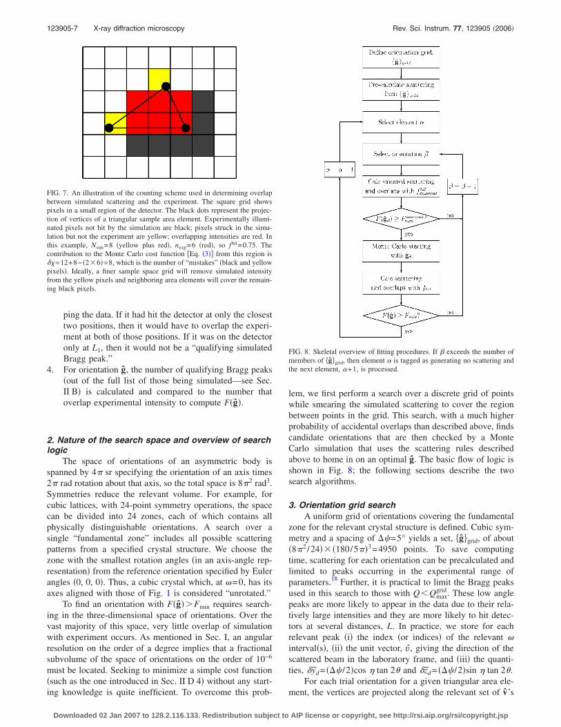
ping the data. If it had hit the detector at only the closesttwo positions, then it would have to overlap the experi-ment at both of those positions. If it was on the detectoronly at L1, then it would not be a “qualifying simulatedBragg peak.”
4. For orientation g, the number of qualifying Bragg peaks�out of the full list of those being simulated—see Sec.II B� is calculated and compared to the number thatoverlap experimental intensity to compute F�g�.
2. Nature of the search space and overview of searchlogic
The space of orientations of an asymmetric body isspanned by 4 sr specifying the orientation of an axis times2 rad rotation about that axis, so the total space is 82 rad3.Symmetries reduce the relevant volume. For example, forcubic lattices, with 24-point symmetry operations, the spacecan be divided into 24 zones, each of which contains allphysically distinguishable orientations. A search over asingle “fundamental zone” includes all possible scatteringpatterns from a specified crystal structure. We choose thezone with the smallest rotation angles �in an axis-angle rep-resentation� from the reference orientation specified by Eulerangles �0, 0, 0�. Thus, a cubic crystal which, at �=0, has itsaxes aligned with those of Fig. 1 is considered “unrotated.”
To find an orientation with F�g��Fmin requires search-ing in the three-dimensional space of orientations. Over thevast majority of this space, very little overlap of simulationwith experiment occurs. As mentioned in Sec. I, an angularresolution on the order of a degree implies that a fractionalsubvolume of the space of orientations on the order of 10−6
must be located. Seeking to minimize a simple cost function�such as the one introduced in Sec. II D 4� without any start-ing knowledge is quite inefficient. To overcome this prob-
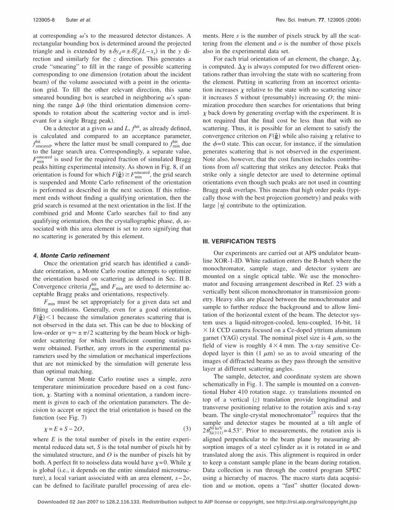
lem, we first perform a search over a discrete grid of pointswhile smearing the simulated scattering to cover the regionbetween points in the grid. This search, with a much higherprobability of accidental overlaps than described above, findscandidate orientations that are then checked by a MonteCarlo simulation that uses the scattering rules describedabove to home in on an optimal g. The basic flow of logic isshown in Fig. 8; the following sections describe the twosearch algorithms.
3. Orientation grid searchA uniform grid of orientations covering the fundamental
zone for the relevant crystal structure is defined. Cubic sym-metry and a spacing of ��=5° yields a set, ggrid, of about�82 /24�� �180/5�3=4950 points. To save computingtime, scattering for each orientation can be precalculated andlimited to peaks occurring in the experimental range ofparameters.18 Further, it is practical to limit the Bragg peaksused in this search to those with Q�Qmax
grid. These low anglepeaks are more likely to appear in the data due to their rela-tively large intensities and they are more likely to hit detec-tors at several distances, L. In practice, we store for eachrelevant peak �i� the index �or indices� of the relevant �interval�s�, �ii� the unit vector, v, giving the direction of thescattered beam in the laboratory frame, and �iii� the quanti-ties, �yd= ��� /2�cos � tan 2� and �zd= ��� /2�sin � tan 2�.
For each trial orientation for a given triangular area ele-ment, the vertices are projected along the relevant set of v’s
FIG. 7. An illustration of the counting scheme used in determining overlapbetween simulated scattering and the experiment. The square grid showspixels in a small region of the detector. The black dots represent the projec-tion of vertices of a triangular sample area element. Experimentally illumi-nated pixels not hit by the simulation are black; pixels struck in the simu-lation but not the experiment are yellow; overlapping intensities are red. Inthis example, Nsim=8 �yellow plus red�, nexp=6 �red�, so fhit=0.75. Thecontribution to the Monte Carlo cost function �Eq. �3�� from this region is� =12+8− �2�6�=8, which is the number of “mistakes” �black and yellowpixels�. Ideally, a finer sample space grid will remove simulated intensityfrom the yellow pixels and neighboring area elements will cover the remain-ing black pixels.
FIG. 8. Skeletal overview of fitting procedures. If � exceeds the number ofmembers of ggrid, then element � is tagged as generating no scattering andthe next element, �+1, is processed.
123905-7 X-ray diffraction microscopy Rev. Sci. Instrum. 77, 123905 �2006�
Downloaded 02 Jan 2007 to 128.2.116.133. Redistribution subject to AIP license or copyright, see http://rsi.aip.org/rsi/copyright.jsp
at corresponding �’s to the measured detector distances. Arectangular bounding box is determined around the projectedtriangle and is extended by ±�yd= ±�yd�L−xs� in the y di-rection and similarly for the z direction. This generates acrude “smearing” to fill in the range of possible scatteringcorresponding to one dimension �rotation about the incidentbeam� of the volume associated with a point in the orienta-tion grid. To fill the other relevant direction, this samesmeared bounding box is searched in neighboring �’s span-ning the range �� �the third orientation dimension corre-sponds to rotation about the scattering vector and is irrel-evant for a single Bragg peak�.
On a detector at a given � and L, fhit, as already defined,is calculated and compared to an acceptance parameter,fsmeared
hit , where the latter must be small compared to fminhit due
to the large search area. Correspondingly, a separate value,Fmin
smeared is used for the required fraction of simulated Braggpeaks hitting experimental intensity. As shown in Fig. 8, if anorientation is found for which F�g��Fmin
smeared, the grid searchis suspended and Monte Carlo refinement of the orientationis performed as described in the next section. If this refine-ment ends without finding a qualifying orientation, then thegrid search is resumed at the next orientation in the list. If thecombined grid and Monte Carlo searches fail to find anyqualifying orientation, then the crystallographic phase, �, as-sociated with this area element is set to zero signifying thatno scattering is generated by this element.
4. Monte Carlo refinementOnce the orientation grid search has identified a candi-
date orientation, a Monte Carlo routine attempts to optimizethe orientation based on scattering as defined in Sec. II B.Convergence criteria fmin
hit and Fmin are used to determine ac-ceptable Bragg peaks and orientations, respectively.
Fmin must be set appropriately for a given data set andfitting conditions. Generally, even for a good orientation,F�g��1 because the simulation generates scattering that isnot observed in the data set. This can be due to blocking oflow-order or �� ± /2 scattering by the beam block or high-order scattering for which insufficient counting statisticswere obtained. Further, any errors in the experimental pa-rameters used by the simulation or mechanical imperfectionsthat are not mimicked by the simulation will generate lessthan optimal matching.
Our current Monte Carlo routine uses a simple, zerotemperature minimization procedure based on a cost func-tion, . Starting with a nominal orientation, a random incre-ment is given to each of the orientation parameters. The de-cision to accept or reject the trial orientation is based on thefunction �see Fig. 7�
= E + S − 2O , �3�
where E is the total number of pixels in the entire experi-mental reduced data set, S is the total number of pixels hit bythe simulated structure, and O is the number of pixels hit byboth. A perfect fit to noiseless data would have =0. While is global �i.e., it depends on the entire simulated microstruc-ture�, a local variant associated with an area element, s−2o,can be defined to facilitate parallel processing of area ele-
ments. Here s is the number of pixels struck by all the scat-tering from the element and o is the number of those pixelsalso in the experimental data set.
For each trial orientation of an element, the change, � ,is computed. � is always computed for two different orien-tations rather than involving the state with no scattering fromthe element. Putting in scattering from an incorrect orienta-tion increases relative to the state with no scattering sinceit increases S without �presumably� increasing O; the mini-mization procedure then searches for orientations that bring back down by generating overlap with the experiment. It isnot required that the final cost be less than that with noscattering. Thus, it is possible for an element to satisfy theconvergence criterion on F�g� while also raising relative tothe �=0 state. This can occur, for instance, if the simulationgenerates scattering that is not observed in the experiment.Note also, however, that the cost function includes contribu-tions from all scattering that strikes any detector. Peaks thatstrike only a single detector are used to determine optimalorientations even though such peaks are not used in countingBragg peak overlaps. This means that high order peaks �typi-cally those with the best projection geometry� and peaks withlarge ��� contribute to the optimization.
III. VERIFICATION TESTS
Our experiments are carried out at APS undulator beam-line XOR-1-ID. White radiation enters the B-hutch where themonochromator, sample stage, and detector system aremounted on a single optical table. We use the monochro-mator and focusing arrangement described in Ref. 23 with avertically bent silicon monochromator in transmission geom-etry. Heavy slits are placed between the monochromator andsample to further reduce the background and to allow limi-tation of the horizontal extent of the beam. The detector sys-tem uses a liquid-nitrogen-cooled, lens-coupled, 16-bit, 1k�1k CCD camera focused on a Ce-doped yttrium aluminumgarnet �YAG� crystal. The nominal pixel size is 4 �m, so thefield of view is roughly 4�4 mm. The x-ray sensitive Ce-doped layer is thin �1 �m� so as to avoid smearing of theimages of diffracted beams as they pass through the sensitivelayer at different scattering angles.
The sample, detector, and coordinate system are shownschematically in Fig. 1. The sample is mounted on a conven-tional Huber 410 rotation stage. xy translations mounted ontop of a vertical �z� translation provide longitudinal andtransverse positioning relative to the rotation axis and x-raybeam. The single-crystal monochromator23 requires that thesample and detector stages be mounted at a tilt angle of2�Si�111�
50 keV =4.53°. Prior to measurements, the rotation axis isaligned perpendicular to the beam plane by measuring ab-sorption images of a steel cylinder as it is rotated in � andtranslated along the axis. This alignment is required in orderto keep a constant sample plane in the beam during rotation.Data collection is run through the control program SPECusing a hierarchy of macros. The macro starts data acquisi-tion and � motion, opens a “fast” shutter �located down-
123905-8 Suter et al. Rev. Sci. Instrum. 77, 123905 �2006�
Downloaded 02 Jan 2007 to 128.2.116.133. Redistribution subject to AIP license or copyright, see http://rsi.aip.org/rsi/copyright.jsp

stream of the monochromator� when the edge of the �� in-terval is reached, and closes it again at the end of thisinterval before the motion is stopped.
The detector is positioned so that the field of view con-tains the direct beam near the bottom edge �as in Fig. 1�. Thismeans that we can observe the incident beam position ateach L via short exposures with the beam stop removed.Also, relatively high-order diffraction will strike the detector;these peaks provide improved projection geometry.
A. Preliminary characterizations
Incident beam. Characterization of the incident beamyields a measure of the CCD detector spatial resolution aswell as the width of the beam in the y direction. We first usea knife-edge scan to determine the incident beam width in z.A 0.5 �m gold film with a sharp edge is scanned across thebeam while Au L-shell fluorescence is monitored with anenergy dispersive detector. The film is rotated about thebeam to make the film edge parallel to the line focused beamby minimizing the width of the fluorescence transition. Theresultant beam profile is well characterized by a sharp centralGaussian plus Lorentzian tails and the height is found to be�2.5 �m FWHM. Figure 9�a� shows the horizontal intensityprofile of the narrowed incident beam �upstream slits wereset to a nominal 100 �m opening� as imaged on the highresolution detector. The intensity is uniform within 3% overthe central 72 �m and the full width at half maximum is98 �m.
Sample and measurement parameters. The sample was asmall piece of a �111�-oriented silicon wafer, 5�3 mm2 incross section and was thinned to �0.2 mm. The sample wasmounted with the �111� axis roughly parallel to the incidentbeam at �=0. Data were collected using ��=1° integrations.We measured 40 such intervals over ±20° in � relative tonormal incidence. For each ��, images were measured at L
�5, 7 , and 9 mm, so there are 120 2MB images. Each im-age and the associated �� motion took 4 s. Data collectionspeed was further limited by the CCD readout time and wasroughly 60 min.
For our range of incidence angles, there is a roughlydiamond-shaped region of sample space that is always illu-minated by the 100 �m wide incident beam as well as adja-cent regions that move into and out of the beam. This pre-sents an analysis challenge since different Bragg peaks donot originate from identical sample regions. We show belowthat we are nevertheless able to isolate the always illumi-nated region with good resolution. Measurements on poly-crystals using a beam wider than the entire sample avoid thiscomplication.
B. Silicon data set and fits
Diffracted beam images. Figure 9 shows images of dif-fracted beams. As expected, the y-direction profile of thediffraction spot is very close to that of the incident beam.The z-direction profiles are foreshortened projections of thewafer thickness in the x direction. The roughly tenfold com-pression of the x-direction geometry implies a similar loss inshape resolution in this direction. Low-order Bragg spotshave a full width at half-maximum in the z direction of �4pixels or �16 �m, which at the angle of observation corre-sponds to a sample thickness of roughly 160 �m. Higher-order spots with small ��� have broader, fully resolved pro-files that more precisely determine the x-directiondimensions of the diffracting entity.
Results. Fits were begun with no a priori informationabout sample orientation. The initially “guessed” orientationcorresponds to crystalline cube axes aligned with the labora-tory coordinate system at �=0. 1594 Bragg peaks out to�Q��14.4 Å−1 or 2�=33.2° were candidates for observationwhile only the lowest-order 300 of these were used in theorientation grid search. The simulation initially coveredsample space with six equilateral triangles with 150 �msides forming a hexagon centered on the rotation axis. Notethat this hexagon is substantially larger than the region illu-minated by the 100 �m wide beam; however, the simulatedbeam width was 200 �m so that scattering from anywhere inthe hexagon can be generated by the simulation. One goal ofthe fitting was for the program to determine the spatial loca-tion of the actual sample, much as it must do in treatingpolycrystal data. Before fitting, area elements were regriddedthree times, yielding 384 triangular elements with 18.75 �msides. After completion of three iterations, the smallest ele-ments were 4.69 �m on a side. After each iteration, experi-mental parameters including the detector distance, L1, androtation axis projections onto the detector, j01, j02, j03 wereadjusted. The intervals L2−L1 and L3−L2 were fixed to themeasured values of 2 mm. The z-direction origins,k01, k02, k03, were fixed to the incident beam positions asimaged on the detector before and after data collection. Priorfits had determined that the detector pixel pitch was 3.78 �mand the beam energy was 49.8 keV. The bandwidth was�1% and was not included in these simulations.
A variety of image analysis and fitting criteria were used.Table I shows values of fpeak and Fmin used and numerical
FIG. 9. Horizontal beam profile and horizontal and vertical diffraction spotprofiles from a silicon wafer. �a� Circles show the horizontal incident beamprofile after summing across the thin vertical width. The solid line is a guideto the eye. The full width at half-maximum is 98 �m. The downward,square, and upward pointing symbols are horizontal profiles of a �311�Bragg spot measured at L1 , L2, and L3, respectively. All profiles have beenshifted to the same center and the incident beam has been normalized to theBragg spots which have been scaled by 103. Since the single-crystal sampleis wider than the beam, the horizontal extent of these spots is essentially thatof the beam. �b� The vertical profile across a �311� Bragg spot �symbols asin �a��. The light line indicates the detector response to the direct incidentbeam; the heavy line is a Gaussian guide to the eye showing that the verticalwidth of the peak is resolved. �c� Vertical profile of a higher-order, �553� or�731� Bragg peak showing the increased width due to larger deflection in thevertical direction.
123905-9 X-ray diffraction microscopy Rev. Sci. Instrum. 77, 123905 �2006�
Downloaded 02 Jan 2007 to 128.2.116.133. Redistribution subject to AIP license or copyright, see http://rsi.aip.org/rsi/copyright.jsp

results of fits. For all fits, fsmearedhit =0.1 and fmin
hit =0.5. Thesimulation generates between 75 and 80 Bragg peaks �de-pending on orientation� that hit at least one detector and38–42 “qualifying Bragg peaks” that hit detectors at multipleL’s �see Sec. II D�. Thus, Fmin=0.5 or 0.75 mean that a gridelement must generate scattering that hits �20 or 30 experi-mental peaks, respectively. For all criteria the software de-termined that a set of area elements near the center of thesimulated hexagon contribute to the observed scattering. Fit-ted orientations are essentially independent of the criteria ofTable I. The nominal Euler angles are �� , ,��= �350.4° ,34.2° ,52.5°�, which correspond to �n ,��= �−0.55,0.33,−0.77,54.3°� in an axis-angle representation.Had the �111� wafer normal been mounted perfectly parallelwith the incident beam direction, the rotation angle wouldhave been cos−1�1/�3�=54.7°. Orientation variation amongfitted elements is small as indicated by the range, ��.
Figure 10 shows sample-space maps corresponding tothe fits listed in Table I. Shading covers triangular grid ele-ments for which qualifying orientations were determined. Inthe color version, the weighting of red, green, and blue �rgb�is determined by the fitted axis-angle pair, �n ,�� for eacharea element. The color scale has been adjusted for eachimage: the full rgb range is scaled to include only the rangeof orientation spanned by the corresponding fit. In all cases,the orientation is uniform over almost all of the fitted region.Comparing Fig. 10�a� and 10�b�, we see that the fitted regionbecomes more compact and regular as the Fmin acceptancecriterion increases. This trend indicates improved signal av-eraging as the number of matched peaks increases; equallyimportant, it indicates that the image analysis and threshold-ing at a uniform fraction of ROI peak height generates aconsistent set of projection contours. In Fig. 10�b�, the fitted
region closely matches the shape of the always illuminatedsubarea of the sample. The left and right truncations are con-sistent with what is known of the thickness of the wafer—about 130 �m. The maximum deviation of edges from thealways illuminated diamond region is 8 �m; the sharpness ofthe upstream �or left� face of the wafer is unresolved whilethe downstream face has deviations of �7 �m. This asym-metry is consistent with the line-shape asymmetry shown inFig. 9: optimal position resolution is associated with sharpBragg spot edges. Even in Fig. 10�b�, deviations of orienta-tion are seen at the edges of the fitted region—this demon-strates a boundary effect in which the orientation at the edgeof a grain or sample can be adjusted slightly to obtain over-lap with a sufficient number of observed peaks. In polycrys-tals, this effect may limit the precision of location of grainboundaries, but near boundary elements can choose whichgrain orientation provides the best fit. Figure 10�c� shows afit to a data set generated with fpeak=0.5. Here, the down-stream side of the sample is missing because the correspond-ing portion of the intensity has been eliminated �Fig. 9�.
Figures 11 and 12 show the diffraction pattern observedin a single �� interval, along with simulation results associ-ated with the maps of Figs. 10�a� and 10�b�, respectively.
TABLE I. Parameters used and results of three fits to silicon single-crystaldata. Corresponding maps are shown in Fig. 10.
Fit fpeak Fmin Fitted elements Fitted area � ��
�mm2� �deg�a �deg�b
a 0.25 0.5 1484 0.044 54.31 0.5b 0.25 0.75 907 0.028 54.32 0.3c 0.5 0.75 270 0.009 54.39 0.2
aAverage rotation from reference orientation.bTotal rotation range of fitted elements.
FIG. 10. Sample-space maps of the illuminated “slot” through the siliconwafer obtained under data reduction and convergence criteria of Table I. Themaps are aligned so that the beam is incident from the left and the wafer isin the yz plane at �=0. The hexagons, with 150 �m sides, indicate thesimulated region of sample space. The + sign indicates the simulated rota-tion axis. The dashed lines show the region of sample space illuminated bythe experimental incident beam as the sample is rotated ±20°. The soliddiamond outlines the region that remains in the beam throughout. Whitespace inside the hexagons has been determined to not satisfy the fittingcriteria for any crystallographic orientation and have been assigned �=0.
FIG. 11. Diffracted beam images at nominal orientation �=−6.5° with fittedintensity corresponding to Fig. 10�a�. In �a�, three images, at L1 , L2 , L3,have been superimposed. Experimental data are shown as black points. Col-ors �or gray scale� show simulated intensity: red, green and blue whenoverlapping experimental data, aqua when not. The line at the bottom indi-cates the projected position of the incident beam at L1; the associated dotindicates the detector origin at �j01 ,k01�= �536,1013�. Bragg spots are seento radiate from the incident beam position at different scattering angles, 2�,and orientations, �. �b� and �c� show expanded views of individual Braggspots; tic marks correspond to 20 pixel intervals; spot positions have beendisplaced for ease of comparison. The reduced height in �c� relative to �b� isdue to the smaller vertical displacement causing a more anisotropic projec-tion in �c�. The at-most subtle broadening of experimental spots with L isconsistent with an energy bandwidth �1%.
FIG. 12. Diffracted beam images at nominal orientation �=−6.5° with fittedintensity corresponding to Fig. 10�b�. All conventions are as in Fig. 11.Here, due to use of more stringent convergence criteria, the simulated in-tensity lies almost entirely within the experimental Bragg spots.
123905-10 Suter et al. Rev. Sci. Instrum. 77, 123905 �2006�
Downloaded 02 Jan 2007 to 128.2.116.133. Redistribution subject to AIP license or copyright, see http://rsi.aip.org/rsi/copyright.jsp
The chosen � interval is atypical in that most intervals con-tain only one or no diffraction peaks from the single crystalsample. Here, five diffracted beams are present at L1, three atL2, and two at L3. One high-order simulated peak �at L1� thatis not in the experimental data set occurs at the right edge;this peak has 2�=29.3° with Miller indices �775� or �11,1,1�and was probably weak enough to be missed in the datareduction. Simulated diffraction spots are expected and seento be smaller than the experimental ones: experimental spotsare projections from the entire illuminated volume of thesample at each �, whereas the simulation includes scatteringonly from those grid elements that remain in the beam anddiffract at many other � positions. At large ��� more of thesample is in the beam and there is more “missed” intensitythan near �=0. As fhit increases, the simulated spots becomesmaller as can be seen in the figures. The entire data set andthese fits can be seen at http://www.andrew.cmu.edu/user/suter/3dxdm/3dxdm.html.
IV. DISCUSSION
We have described and verified a method that shouldallow nondestructive internal microstructure mapping in awide variety of sample types. Our current analysis softwareclosely mimics the measurement and can account for a vari-ety of experimental and sample complexities. Here, we havedemonstrated the ability to resolve, to �10 �m, the shape ofa region of sample with “soft” edges. Three dimensionalmaps of more interesting samples are a straightforward ex-tension of this work; in fact, we have recently succeeded inreconstructing a significant volume of microstructure in analuminum polycrystal sample.25 Many applications suggestthemselves, including fundamental studies of grain growthcoupled to three-dimensional computer simulations,12,13 re-sponse of microstructure to stress of a variety of types, andthe structure of polyphase materials and solid-state phasetransformations. In each case, it should be possible to studythe response of three-dimensional, interconnected ensemblesof grains.
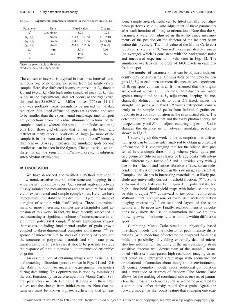
An essential part of obtaining images such as in Fig. 10and matching diffraction spots as shown in Figs. 11 and 12 isthe ability to optimize uncertain experimental parametersduring data fitting. This optimization is done by minimizingthe cost function, , via zero temperature Monte Carlo. Sev-eral parameters are listed in Table II along with their fittedvalues and the change from initial estimates. Note that pa-rameters must be known a priori sufficiently that at least
some sample area elements can be fitted initially; our algo-rithm performs Monte Carlo adjustment of these parametersafter each iteration of fitting to orientations. Note that the k0
parameters were not adjusted in these fits since measure-ments of the position on the detector of the incident beamdefine this precisely. The final value of the Monte Carlo costfunction, , yields �330 “missed” pixels per detector image�on average� which is consistent with the background noiseand uncovered experimental pixels seen in Fig. 12. Thesimulation overlaps on the order of 1400 pixels in each dif-fraction spot.
The number of parameters that can be adjusted indepen-dently may be surprising. Optimization of the detector ori-gins �j0 ,k0� at each measurement distance makes experimen-tal Bragg spots colinear in L. It is assumed that the originsare constant across all � so these adjustments are madeagainst many fitted spots. L1 adjustment, keeping the me-chanically defined intervals to other L’s fixed, makes thestraight line paths with fixed 2� values extrapolate consis-tently to the sample and peaks from individual grains ex-trapolate to a common position in the illuminated plane. Thedetector calibration constant and the x-ray photon energy areindependent: � and E both adjust scattering angles but E alsochanges the distance in � between simulated peaks, asshown in Fig. 3.
Underlying all this work is the assumption that diffrac-tion spots can be consistently analyzed to obtain geometricalinformation. It is encouraging that for the silicon data pre-sented here a simple thresholding scheme yields quite pre-cise geometry. Silicon has classes of Bragg peaks with inten-sities different by a factor of 2 and intensities vary with Qdue to form factor and lattice vibration effects, so an inde-pendent analysis of each ROI in the raw images is essential.Complex line shapes in interesting materials most likely pre-clude any universally correct threshold fraction, fpeak. Someself-consistency tests can be imagined: in polycrystals, toohigh a threshold should yield maps with holes, so one maybe able to adjust fpeak downward to just obtain completion.Without doubt, comparisons of x-ray data with orientationimaging microscopy9,10 on sectioned layers of the samesample will be necessary. Finally, realistic intensity calcula-tions may allow the use of information that we are nowthrowing away—the intensity distributions within diffractionspots.
Combining Monte Carlo simulation, physically basedline-shape models, and the inclusion of peak intensity distri-butions �with modeling of detector point-spread functions�holds the possibility of yielding extremely detailed micro-structure information. Including in the measurement a strainsensitive detector well downstream of the sample26 �com-bined with a semitransparent high-resolution imaging detec-tor� could yield intragrain strain maps with geometric andorientational information about intergranular environments.Of course, complex models imply additional computationand a multitude of degrees of freedom. The Monte Carloallows for the making of correlated moves on sets of param-eters that cross area elements such as would be generated bya continuous defect density model for a grain. Again, theforward model has the robust feature that changing one scat-
TABLE II. Experimental parameters obtained in the fit shown in Fig. 12.
Parameter Units Fitted value Change�a ��m/pixel� 3.78 −0.22
�j0 ,k0�1 pixels �531.8, 1013.5� �−3.2,0��j0 ,k0�2 pixels �534.7, 1013.5� �−0.3,0��j0 ,k0�3 pixels �537.0, 1012.5� �2.0, 0�
L1 mm 5.04 0.04E keV 49.8 −0.2 39605b
aDetector pixel pitch calibration.bReduced data hit 48685 pixels.
123905-11 X-ray diffraction microscopy Rev. Sci. Instrum. 77, 123905 �2006�
Downloaded 02 Jan 2007 to 128.2.116.133. Redistribution subject to AIP license or copyright, see http://rsi.aip.org/rsi/copyright.jsp

tering parameter will generate changes in all the scatteringgenerated by the grain or area element. Finally, a dynami-cally optimized finite temperature Monte Carlo27 provides ameans for gaining efficiency, determining correlationsamong parameters, and estimating errors.
Facilities at the Advanced Photon Source, while ad-equate for the silicon measurements presented here and pre-liminary work on polycrystals, are currently being upgraded.A high-precision air bearing rotation stage with submicrome-ter errors is being commissioned. Refractive focusing opticshave been developed that allow further reduction in the en-ergy band pass. Purchase of a CCD camera with more rapidreadout is planned as is the design of a semitransparent scin-tillator system that will allow combined mapping and strainmeasurements. In the longer term, an undulator source tai-lored for high energies is planned. These upgrades will speeddata collection and further improve spatial and angularresolution.
ACKNOWLEDGMENTS
We thank the personnel at Sector 1, particularly JonAlmer, Kamel Feeza, and Ali Mashayekhi, for their valuableassistance. We have benefited from conversations with H. F.Poulsen, A. D. Rollett, G. S. Rohrer, M. Widom, S. Garoff,and J. Sethna. This work was supported primarily by theMRSEC program of the National Science Foundation underAward No. DMR-0520425. Use of the Advanced PhotonSource was supported by the U.S. Department of Energy,Basic Energy Sciences, Office of Science, under ContractNo. W-31–109-Eng-38.
1 H. F. Poulsen, Three-Dimensional X-ray Diffraction Microscopy, SpringerTracts in Modern Physics, Vol. 205, edited by G. Hohler �Springer, NewYork, 2004�.
2 H. F. Poulsen, X. Fu, E. Knudsen, E. M. Lauridsen, L. Margulies, and S.Schmidt, Mater. Sci. Forum 467–470, 1363 �2004�.
3 B. Jakobsen, H. F. Poulsen, U. Lienert, J. Almer, S. D. Shastri, H. O.Sørensen, C. Gundlach, and W. Pantleon, Science 312, 889 �2006�.
4 L. Margulies, G. Winther, and H. F. Poulsen, Science 291, 2392 �2001�;see also the associated “Perspective” by F. Heidelbach, ibid. 291, 2330�2001�.
5 S. Schmidt, S. F. Nielsen, C. Gundlach, L. Margulies, X. Huang, and D.Juul Jensen, Science 305, 229 �2004�.
6 S. E. Offerman, N. H. van Dijk, J. Sietsma, S. Grigull, E. M. Lauridsen, L.Margulies, H. F. Poulsen, M. Th. Rekveldt, and S. van der Zwaag, Science298, 1003 �2002�.
7 T. Kubo, E. Ohtani, and K. Funakoshi, Am. Mineral. 89, 285 �2004�.8 E. M. Lauridsen, S. Schmidt, R. M. Suter, and H. F. Poulsen, J. Appl.Crystallogr. 34, 744 �2001�.
9 H. F. Poulsen, S. F. Nielsen, E. M. Lauridsen, S. Schmidt, R. M. Suter, U.Lienert, L. Margulies, T. Lorentzen, and D. Juul Jensen, J. Appl.Crystallogr. 34, 751 �2001�.
10 G. S. Rohrer, Annu. Rev. Mater. Res. 35, 99 �2005�.11 See also http://mimp.materials.cmu.edu/ and publications listed thereon.12 J. Gruber, D. C. George, A. P. Kuprat, G. S. Rohrer, and A. D. Rollett, Scr.
Mater. 53, 351 �2005�.13 D. Kinderlehrer, J. Lee, I. Livshits, and S. Taasan, in Continuum Scale
Simulation of Engineering Materials: Fundamentals—Microstructures—Process Applications, edited by D. Raabe, F. Roters, F. Barlat, and L.-Q.Chen �Wiley-VCH, Berlin, 2004�, pp. 356–367.
14 G. E. Ice, B. C. Larson, W. Yang, J. D. Budai, J. Z. Tischler, J. W. L. Pang,R. I. Barabash, and W. Liu, J. Synchrotron Radiat. 12, 155 �2005�.
15 L. E. Levine, B. C. Larson, W. Yange, M. E. Kassner, J. Z. Tischler, M. A.Delos-Reyes, R. J. Fields, and W. Liu, Nat. Mater. 5, 619 �2006�.
16 H. O. Sørensen, B. Jakobsen, E. Knudsen, E. M. Lauridsen, S. F. Nielsen,H. F. Poulsen, S. Schmidt, G. Winther, and L. Margulies, Nucl. Instrum.Methods Phys. Res. B 246, 232 �2006�.
17 H. F. Poulsen and F. Xiaowei, J. Appl. Crystallogr. 36, 1062 �2003�.18 S. Schmidt, H. F. Poulsen, and G. B. M. Vaughan, J. Appl. Crystallogr.
36, 326 �2003�.19 T. Markussen, X. Fu, L. Margulies, E. M. Lauridsen, S. F. Nielsen, S.
Schmidt, and H. F. Poulsen, J. Appl. Crystallogr. 37, 96 �2004�.20 X. Fu, E. Knudsen, H. F. Poulsen, G. T. Herman, T. Gabor, B. M. Car-
valho, and H. Y. Liao, Proc. SPIE 5535, 261 �2004�.21 A. Alpers, E. Knudsen, G. T. Herman, and H. F. Poulsen, J. Appl.
Crystallogr. 39, 582 �2006�.22 N. K. Roy and R. M. Suter �unpublished�.23 U. Lienert, C. Schulze, V. Honkimaki, T. Tschentscher, S. Garbe, O.
Hignette, A. Horsewell, M. Lingham, H. F. Poulsen, N. B. Thomsen, andE. Ziegler, J. Synchrotron Radiat. 5, 226 �1998�.
24 We take the variation in angle of incidence, � to be the difference inscattering angles for radiation from the �111� planes of a silicon mono-chromator crystal: � =2�−2�0=2G111
Si �1/2k−1/2k0�. Energies greaterthan the nominal have � �0, corresponding to having ki
z�0. This for-mula approximates the incoming white beam as being parallel.
25 R.M. Suter, C. Hefferan, D. Hennessy, C. Xiao, U. Lienert, in preparation.26 R. V. Martins, L. Margulies, S. Schmidt, H. F. Poulsen, and T. Leffers,
Mater. Sci. Eng., A 387–389, 84 �2004�.27 D. Bouzida, S. Kumar, and R. H. Swendsen, Phys. Rev. A 45, 8894
�1992�.
123905-12 Suter et al. Rev. Sci. Instrum. 77, 123905 �2006�
Downloaded 02 Jan 2007 to 128.2.116.133. Redistribution subject to AIP license or copyright, see http://rsi.aip.org/rsi/copyright.jsp


