
for - NASA · · 2017-06-26A s si stant Project ... Frequency Characteristics Versus Input...
61
1IIIpo.QILoQ<4OO"ICTIOVT lA8.A. -- #- e -PI 1 1 ' I Hamilton Standard -Q- - _" -- for https://ntrs.nasa.gov/search.jsp?R=19650024618 2018-06-27T04:31:07+00:00Z
Transcript of for - NASA · · 2017-06-26A s si stant Project ... Frequency Characteristics Versus Input...

1IIIpo.QILoQ<4OO"ICTIOVT lA8.A.
- - #- e -PI 1 1 ' I Hamilton Standard -Q-
- _" --
for
https://ntrs.nasa.gov/search.jsp?R=19650024618 2018-06-27T04:31:07+00:00Z

NONDISSIPATIVE DC TO D C REGULATOR -CONVERTER STUDY
HSER 3124
THIRD QUARTERLY REPORT 15 DECEMBER 1964 TO 15 AUGUST 1965
CONTRACT NO. NAS 5-3921
GODDARD SPACE FLIGHT CENTER GREENBE LT, MARY LAND
P r e p a r e d By # T d I P- F r a n k L. Rapo'sa A s si s tant P r o j e c t Engineer
Approved By: f, & William E. Michel P r o j e c t Enginee r
HAMILTON STANDARD DIVISION UNITED AIRCRAFT CORPORATION
BROAD BROOK, CONNECTICUT

HSER 3124
I. ABSTRACT
The e f f o r t i n the third quar te r ly per iod included the following:
1. Ini t ia l Breadboard development of the self- stabil izing chopper power Stage.
Evaluat ion of s e v e r a l f requency control stages.
T e s t and evaluation of the frequency-efficiency c h a r a c t e r i s t i c s of the self-s tabi l iz ing chopper.
Size and weight ana lys i s of the self-s tabi l iz ing chopper.
2.
3.
4.
The r e s u l t s of the effor t for this qua r t e r ly per iod a r e :
1.
2.
3.
4.
The final configuration for the power s tage is a single-ended self-s tabi l iz ing chopper. The bas i c se l f - stabil izing concept r e q u i r e s a means of c i rcu i t s ta r t ing f o r each half cycle; a n ex- t e rna l ga t e t r i g g e r pu lse i s uti l ized f o r th i s purpose. A m e a n s of c u r r e n t l imiting is required to p reven t c i r cu i t r ecove ry t ime lag of the self- stabilizing chopper; a degenerat ive feedback c u r r e n t limit method i s utilized fo r th i s purpose.
A sa tura t ing c o r e squa re wave osc i l la tor has been se lec ted fo r this phase of the p r o g r a m as the var iab le frequency source.
The frequency-efficiency cha rac t e r i s t i c s of the 10-watt self- stabil izing chopper show relat ively small changes in peak efficiency at minimum l ine voltage but significant changes in efficiency at maximum l ine voltage.
The nominal switching frequency of the 10-watt chopper regula tor shouldbe at l e a s t 25 KC to in su re meet ing the design goa l com- ponent weight of 0.63 pounds. The component volume es t ima te at 25 KC is approximately 6 cubic inches which is wel l under the 15 cubic inch design goal.
ii

HSER 3124
SE C TION
TABLE O F CONTENTS
TITLE PAGE
I
I1
I11
I V
Abs t r ac t
Pu rpose
Introduction
Technical Discussion
ii
1
2
m v VI
VI1
VI11
IX
A. Init ial Development of the Self Stabilizing Chopper Power Stage
Be Frequency Control Stages
C. Frequency -Efficiency Charac te ri s t ic s
D. Size and Weight Analysis
Conclu s io n s and R e c ommenda ti ons
P r o g r a m f o r Next Interval
Bibliography
Co nf e r enc e s
New Technology
3
26
35
44
52
53
54
55
55

HSER 3124
LIST O F TABLES AND ILLUSTRATIONS
TABLE
1.
2.
3.
4.
5.
6.
7.
8
9.
10.
FIGURE
1.
2.
3.
4.
5.
6.
7.
TITLE PAGE
Magnetic P rope r t i e s for Switching Cores
RMS Drive Current fo r Different Curren t Limiting Approaches 17
Efficiency Data for 5 KC Frequency Efficiency Tes t 36
Efficiency Data for 10 KC Frequency Efficiency Tes t 37
8
Efficiency Data for 20 KC Frequency Efficiency Tes t
Efficiency Data for 30 KC Frequency Efficiency Tes t
Weight and Volume Analysis of the Frequency Control Stage 46
Weight and Volume Analysis of the Dr ive r / Gate
38
39
Stage 47
Weight and Volume ana lys is of the Chopper P o w e r Stag e 48
Weight and Volume Analysis of the Output F i l t e r Stage 49
TITLE PAGE
Bas ic Self Stabilizing Chopper P o w e r Stage
Modified Self Stabilizing Chopper Power Stage
Self Stabilizing Chopper Power Stage Using Gate P u l s e Starting
C u r r e n t Response for a Square Loop Core to a Constant Voltage Excitation
Saturation Charac te r i s t ic of F e r r i t e Dr iver T r a n s - f o r m e r
Saturat ion Character is t ic of Del tamax D r i v e r T r a n s f o r m e r
No Cur ren t Limiting
4
4
6
8
10
11
13

HSER 3124
LIST O F TABLES AND ILLUSTRATIONS ( Continued )
FIGURE TITLE PAGE
8. Res is t ive Cur ren t Limiting 13
9. D eg e ne ra ti v e F e e d ba c k C u r r e n t Limiting 14
10. T r a n s i s t o r Cur ren t Limiting 14
11.
12
13.
14.
15.
16.
17.
18.
19.
2 0.
21
22.
23,
Col lec tor -Emi t te r Voltage Waveform and Collector C u r r e n t Waveform of Chopper D r i v e r Stage With No C u r r e n t Limiting 18
Col lec tor -Emi t te r Voltage Waveform and Collector Cur ren t Waveform of Chopper D r i v e r Stage With 5 f i C u r r e n t Limiting 19
Collecto r - E m i t t e r Voltage Waveform and Collector C u r r e n t Waveform of Chopper D r i v e r Stage With 2 6 h Emitter Feedback 20
F requency Charac te r i s t ics V e r s u s Input Voltage 21
Single Ended Self-stabilizing Chopper
Unijunction Trans i s to r Relaxation Os cil lato r
A s table Multivibrator Os cil lato r
Sa tu ra ting Cor e Square Wave 0 s cil la to r
Fu l l Load Efficiency V e r s u s Input Voltage
No Load L o s s e s Versus Input Voltage
Efficiency of 30 KC Chopper Under Varying Loads
Sys t em Schematic for S ize and Weight Analysis
S u m m a r y of Size and Weight Analysis of 10 W a t t Chopper Regulator
24
27
30
33
40
4 2
43
50
51

HSER 3124
11. P U R P O S E -
, The purpose of this p r o g r a m is to provide concepts , techniques, and developed modular c i r c u i t r y f o r non-dissipative DC to DC conver t e r s i n the power range of 0 to 100 watts.
Major p r o g r a m goals a r e the maximization of efficiency, simplicity, and rel iabi l i ty , along with minimizat ion of s i ze , weight, and response t i m e s of the conver te rs .
The c i r cu i t s a r e to be modular i n concept, so that a minimum of development is requi red to ta i lor a c i rcu i t to a specif ic application requirement . The concepts should also allow, inasmuch as prac t ica l , fo r the use of s t a t e -o f - the -a r t manufacturing techniques.
The p r o g r a m is mult i -phased, including a s t u d y , ana lys i s , and des ign phase , and a breadboard phase during which the concepts a r e to be ver i f ied by construct ion and t e s t of eight breadboards .
1

HSER 3124
111. INTRODUCTION
The work of the previous q u a r t e r included the following:
1.
2. Frequency control s tages
Initial development of the self- stabil izing chopper power stage.
3. Frequency-eff ic iency cha rac t e r i s t i c s of the self-s tabi l iz ing chopper regulator.
4. Size and weight ana lys i s of the self-s tabi l iz ing chopper regula tor
Seve ra l p roblem a r e a s with the self-stabil izing scheme w e r e uncovered e a r l y in the breadboard development phase which requi red extensive investigations. The p rob lems w e r e associated with c i r cu i t s ta r t ing , c i r cu i t r ecove ry t ime, and balanced operation. Solutions to each of these p rob lems were- de te rmined ,
Breadboard invest igat ions of severa l var iable f requency s o u r c e s w e r e made to de te rmine the m o s t applicable frequency s o u r c e f o r t h i s phase of the program. t r a n s i s t o r -relaxation osc i l l a to r , the as tab le mul t iv ibra tor osc i l la tor , and the sa tura t ing c o r e squa re wave oscil lator.
The following c i rcu i t s w e r e cons idered; the unijunction
0 The frequency-efficiency cha rac t e r i s t i c s of the self- stabil izing chopper
T e s t s were run a t nominal switching frequencies regula tor w e r e obtained. of 5 , 10, 20, and 30 KC.
A s i z e and weight ana lys i s of the self-stabil izing chopper regula tor was obtained for the above nominal switching frequencies. the frequency-efficiency tes t ing and of the s i z e and the s i z e and weight ana lys i s w e r e used to de t e rmine the opt imum switching frequency for the chopper regulator.
Resul t s of
2

HSER 3124
1,V TECHNICAL DISCUSSION
A. INITIAL DEVELOPMENT OF THE S E L F STABILIZING CHOPPER
The b a s i c self stabil izing chopper power s tage shown i n f igure 1, cons is t s of two power t r a n s i s t o r s Ql and c22, two d r i v e r t r a n s i s t o r s Q3 and Q4 and a b a s e d r ive t r a n s f o r m e r T1. supplied to Q1 and Q2. constant volt second product of the saturat ing co re d r ive t r ans fo rmer . The volt second product of th i s t r a n s f o r m e r i s capable of sustaining a voltage of E volts fo r a t i m e of t seconds. If E i n c r e a s e s t must d e c r e a s e to maintain the constant volt second product ; hence; automatic s tabi l izat ion i s accomplished fo r input l ine variations.
R e s i s t o r s R2 and R4 control the b a s e c u r r e n t Self stabil ization of the chopper i s obtzined through the
A descr ip t ion of ci r cu i t operat ion follows; a s s u m e t r a n s i s t o r Q3 i s biased i n the fo rward direction. sufficient t o t u r n on t r a n s i s t o r Q2 slightly, p a r t of voltage E will be applied a c r o s s t r a n s f o r m e r T1. t r a n s i s t o r Q2 into saturat ion and delivering power to the load. t r a n s i s t o r 0 2 is maintained for E t volt-seconds until t r a n s f o r m e r TI sa tura tes . Dr ive voltage for t r a n s i s t o r Q2 col lapses a f t e r sa tura t ion of the d r ive t r a n s f o r m e r , thus turning t r a n s i s t o r Q2 off. s t a t e until t r a n s i s t o r Q4 becomes energized, energ ized the cycle r epea t s i tself with t r a n s i s t o r Q1 del iver ing power to the load. each half cycle,
If the leakage c u r r e n t through r e s i s t o r R3 i s
Cur ren t will flow through t r a n s i s t o r 0 3 thus driving Dr ive voltage fo r
The chopper c i rcu i t i s forced into a cut-off When t r a n s i s t o r Q4 becomes
0 Note that s ta r t ing of the self-stabil izing chopper i s requi red to ini t ia te
S e v e r a l p rob lem a r e a s with the self stabil izing chopper scheme w e r e
A second problem was assoc ia ted with uncovered e a r l y i n the breadboard development phase. a s soc ia t ed with c i rcu i t start ing. insur ing rapid t u r n off of the self stabilizing chopper after the d r ive t r a n s f o r m e r T1 had saturated. output of the push-pull s tage consisting of t r a n s i s t o r s Ql and Q2.
One p rob lem was
A th i rd problem was assoc ia ted with obtaining a balanced
C i rcu i t S ta r t ing P r o b l e m
An ex te rna l m e a n s of s ta r t ing the self-stabil izing chopper i s requi red to in i t ia te each half cycle of operation. This i s n e c e s s a r y s ince the sa tura t ion of the d r i v e t r a n s f o r m e r T1 during the prev ious half cycle shuts off the main chopper t r ans i s to r s . r e s i s t o r s R 1 and R3 to energ ize t r a n s f o r m e r T1.
The c i r cu i t shown i n f igure 1, depends on leakage through
This method of s ta r t ing was found to be unsat isfactory during the p re l imina ry The component res i s tance values of R1 and R3 had to be s e t b readboard stages.
at re la t ive ly low values to ini t ia te c i rcu i t t u r n on. va lues of t hese r e s i s t o r s produced shfficient b a s e d r ive f r o m the main supply voltage to keep the chopper t r a n s i s t o r s switched on independent of the d r ive voltage provided by the d r ive t r a n s f o r m e r T1,
However , the resu l tan t
3

R \
R2
R3
fw
F i g u r e 1 BASIC SELF STABILIZING CHOPPER POWER STAGE
Figure 2 MODIFIED S E L F STABILIZING CHOPPER POWER STAGE
4

HSER 3124
The modification shown in f igure 2 , w a s t r i ed to solve this s ta r t ing problem. al.ternate s ta r t ing r e s i s t o r RS. Res i s to r RS was connected d i r ec t ly a c r o s s t r a n s i s t o r s Q1 and Q2 to lead the main supply voltage d i rec t ly to the p r i m r y of t r a n s f o r m e r T1. The intended solution was to s e t r e s i s t o r RS to a v a l u e low enough to provide sufficient leakage around t r a n s i s t o r s Ql and Q2 to energ ize t r a n s f o r m e r T1. Note, however, that RS has now provided a d i r e c t coupling path between input and output.
This modification eliminated r e s i s t o r s R 1 and R3 and added a n
This method of c i r cu i t s ta r t ing was breadboarded and evaluated. It w a s de te rmined tha t the r e s i s t ance value w a s dependent on the input voltage. example, at 10 volts input i t was found tha t RS had to be s e t as low a s 3 0 A to provide sufficient t u r n on drive. the r equ i r emen t fo r a small value of RS would provide low impedance coupling between the input and output of the circuit.
FOP
This approach w a s d i sca rded because
The modification shown in f igure 3 , w a s investigated a.s another poss ib le solution to the s ta r t ing problem. r a t h e r than the fixed leakage coupling previous ly discussed. The ga te pulse , which i s coupled through diodes D1 and D2, momentar i ly connects the supply voltage to the b a s e s of t r a n s i s t o r s Q1 and Q2. momentar i ly d r iven on, thus allowing the supply voltage to be i m p r e s s e d a c r o s s t r a n s f o r m e r T1.
This c i r cu i t utilized a ga te pulse input
These t r a n s i s t o r s a r e
The regenera t ion p r o c e s s i s init iated and the c i r cu i t ope ra t e s - 0 as previous ly descr ibed.
The ga te pulse i s synchronized to the va r i ab le f requency squa re wave s o u r c e so that the ga t e pulse i s applied at the s a m e ins tan t tha t e i the r t r a n s i s t o r Q3 o r Q4 i s forward biased.
Sa t i s fac tory s ta r t ing cha rac t e r i s t i c s w e r e obtained with th i s s ta r t ing method. s ta r t ing technique.
A l l f u r the r breadboard testing was done using the ga te pulse
Ci rcu i t Recoverv T i m e Lag Prob lem
The finite r ecove ry t i m e of the main chopper t r a n s i s t o r s , a f t e r the d r i v e r t r a n s f o r m e r T1 has saturated, r e s u l t s ir, a t r ans i en t low impedance condition exis t ing a c r o s s the input voltage. sp ike to be d rawn through the d r ive r t r ans fo rmer , in t roduces a n additional t ime delay in c i r cu i t recovery t ime , thus resul t ing in significant power l o s s e s f o r the system. indicated tha t i f th i s c u r r e n t pu lse could b e l imi ted , the r ecove ry t i m e of the chopper c i r cu i t could be increased , and the power l o s s e s assoc ia ted with th i s r e c o v e r y lag could be minimized.
Thi s causes a l a r g e c u r r e n t This c u r r e n t spike
P r e l i m i n a r y breadboard tes t ing
Invest igat ions w e r e conducted to de t e rmine solutions to th i s problem. The invest igat ions involved s tudies of both the inherent c h a r a c t e r i s t i c s of the d r i v e r t r a n s f o r m e r , and of c i rcu i t methods for achieving s o m e f o r m of - c u r r c n t l imiting. e 5

H S E R 3124
F i g u r e 3 SELF S T A B I L I Z I N G C H O P P E R P O W E R S T A G E USING G A T E P U L S E S T A R T I N G
6

HSER 3124
D r i v e r T r a n s f o r m e r Investigation
The invest igat ion conducted into the d r ive r t r a n s f o r m e r was made to de t e rmine what effect on the cu r ren t pulse the inherent c h a r a c t e r i s t i c s the t r a n s f o r m e r might have. h a s been repor ted i n de ta i l by S t r a u s s l . sa tura t ion o c c u r s , of the c u r r e n t drawn into a n open circui ted t r a n s f o r m e r excited by a s tep voltage of constant amplitude i s given by:
Studies on the t e r m i n a l r e sponse of switching c o r e s An approximation up to where
d v 2 t + tLl. N i(t) = -
8E33 h2 Bs After sa tura t ion o c c u r s the c u r r e n t drawn i s de te rmined by:
V - ‘t) where
d = conductivity of the c o r e 1 = length of c o r e V = applied voltage N = number of t u r n s h = w i d t h of c o r e B s = maximum flux densi ty
R = source r e s i s t ance (including winding r e s i s t ance ) L c inductance of coi l i n air
H C = coerc ive MMF
The above equation fo r c u r r e n t drawn up to sa tura t ion h a s been der ived based on the following assumpt ions :
1. The r ad ius of cu rva tu re of the c o r e is l a r g e c o p p a r e d to the thickness of the co re d.
2. The width of the c o r e h i s much g rea t e r than the thickness of the co re d.
3. The h y s t e r e s i s loop i s perfect ly rectangular.
4. The c o r e i s ini t ia l ly magnetized a t -Bs and switches to tB,.
5. The field pene t r a t e s at equal r a t e s f rom both ins ide and outs ide of the core.
F i g u r e 4 shows the t e r m i n a l c u r r e n t response of the square- loop c o r e to a constant voltage excitation. where IC i s the c u r r e n t due the coerc ive MMF. and the c u r r e n t r i s e s exponentially to a steady s t a t e value de te rmined by the magnitude of the applied voltage and the magnitude of the source res i s tance . The s lope of the l i n e a r port ion of the curve i s de te rmined by the geomet ry of
The cur ren t begins r i s ing l inear ly f r o m I C , A t ts s a t ~ ~ r a t i p n ~ c c u r s
the c o r e , its conductivity, and the magnitude squared of t h e applied voltage. 1. ) S t r a u s s , L e o n a r d Wave Generat ion and Shaping, New York, McGraw-Hill , 1960.
7

~ ~~~
HSER 3124
Del tamax
P e rma l loy
F e r r i t e IG C - 2
i
4 5 p X l - c m 15, 500 gauss
55pA2-crn 8, 000 g a u s s
I O O S 5 - c m 2 , 7 5 0 g a u s s
I I I I
0. 16 oe r s t eds
0. 0 i o e r s t e d s .
0. 36 oe r s t eds
I I
tS t
0.98 typical
0. 90 typical
0. 91 typical
0.50-
Figure 4 Cur rex t Respor?se of 5 Square Loop Core To A Constant Voltage Exci ta t ion
TABLE 1 MAGNETIC PROPERTIES FOR SWITCHING CORES
-- Sa t u ra tio n
CO re Mate rial Volnxne F l u x Densi tv
C..
Coercive Squa r e n e s s MMF Ratio
I I i
8

HSER 3124
The t ime constant of the exponential rise is de te rmined by the equivalent sou rce r e s i s t ance and the inductance of the coil ir, air. This t i m e constant is normal ly ve ry small, s ince the air coi l inductance of a- small toroid i s normal ly in the mic rohenry range.
F o r a given t r a n s f o r m e r core ma te r i a l ( C = constant) , the m o s t p r e -
A t r a c s f o r m e r des ign requi r ing a l a r g e dominant t e r m number of t a r n s of the winding. number of t u r n s would have a two fold effect ; reduct ion of the coerc ive c u r r e n t constant, s ince th i s is inverse ly proport ional to N: and reduction of the s lope of the eddy c u r r e n t , s ince this i s inverse ly propor t iona l t o the ccrbe of N. A des ign c r i t e r i a f o r a. l a r g e number of t u r n s would r equ i r e a t r a n s f o r m e r of small- c o r e a r e a fo r a given co re ma te r i a l and excitatiori voltage. the reduction of c o r e a r e a would have to be made by making the thickness d ve ry small while keeping the width h l a r g e , s ince the width I-, i s ais0 a n impor t ac t t e r m in reducing the eddy c i i r ren t slope. Investigations of f rac t iona l m i l bobbin c o r e s have shown this condition difficult to meet , s ince the width to th ickness ratio h /d is normally 4. 5 So 1.
of the above equztion fo r l imit ing the c u r r e n t i s N , the
However ,
Table 1 shown some typical magnetic p r o p e r t i e s of s e v e r a l m a t e r i a l s tha t w e r e investigated for this application. above equation showed that the finite c o r e would r e q u i r e the l e a s t c u r r e n t at sa tura t ion s ince i t s volume resis t ivi ty is s e v e r a l o r d e r s of magnitl;de g r e a t e r than the o the r magnet ic mater ia l s . showed that the final s teady s ta te cu r ren t drawn a f t e r sa tura t ion would be about the same f o r each core.
P r e l i m i n a r y calculat ions using the
0 P r e l i m i n a r y calculat ions a l s o
T e s t compar isons w e r e made between a de l tamax and f e r r i t e core . The sa tu ra t ion c h a r a c t e r i s t i c s f o r a del tamax and a f e r r i t e d r i v e r t r a n s f o r m e r , b readboarded f o r the 10-watt chopper, a r e shown i n f igu res 5 and 6. sa tura t ion c h a r a c t e r i s t i c of the del tamax c o r e shows a much m o r e rapid t u r n off t ime than the f e r r i t e core. This f a s t e r t u r n off t i m e is probably a t t r ibu ted to the higher squa reness ratio of the de l tamax coreo of the t u r n off slope showed that the del tamax t r a n s f o r m e r had a tu rn off slope of 4 volts p e r microseconds compared to 2 v o l t s p e r microsecond fo r the f e r r i t e t r ans fo rmer . de l t amax c o r e m a t e r i a l s provide the m o s t des i r ab le cha rac t e r i s t i c s for t h i s c i r cu i t application. to th i s p rob lem util ized this co re mater ia l .
The
Measuremen t s
The r e su l t s of t hese t e s t s have indicated tha t
A l l f u r the r efforts made i n determining the solution
9

HSER 3124
0
Waveform A c r o s s P r i m a r y of T r a n s f o r m e r Vert ical Scale: 10 voI t s / cm
Horizontal Scale: 10 p s e c / c m
0
Collector -Emitter Wavefo rm Ver t ica l Scale: 5 vo l t s / cm
Horizontal Scale; 10 p s e c / c m
F igure 5 Saturat ion Charac te r i s t ic of F e r r i t e D r i v e r T ran sfo r m e r
10

HSER 3124
Waveform Across Primary of Transformer Vertical Scale: 10 volts/cm
Horizontal Scale: 10 psec./cm
Colle c to r -E mi tte r Wave fo rm Vertical Scale: 5 volts/cm
Horizontal Scale: 10 psec/cm
Figure 6 Saturation Characteristic of D eltama x D river T ran sf o rm er
HSER 3124
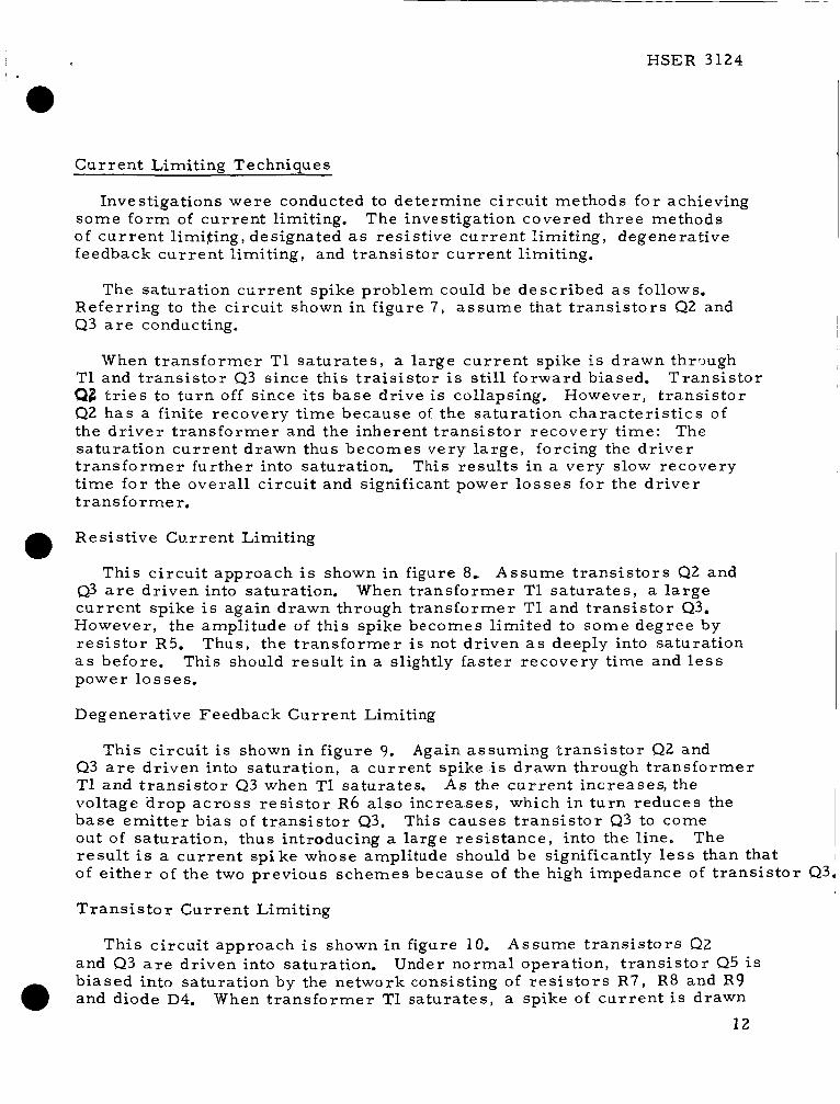
Cur r e n t Limit ing Techniques
Invest igat ions w e r e conducted to de te rmine c i r cu i t methods f o r achieving s o m e f o r m of c u r r e n t limiting. of c u r r e n t limi$ing, designated as res i s t ive c u r r e n t l imit ing, degenera t ive feedback c u r r e n t l imit ing, and t r ans i s to r c u r r e n t l imiting.
The investigation covered th ree methods
The sa tura t ion cGrrent spike problem could be desc r ibed a s follows. Refer r ing to the c i rcu i t shown in f igure 7 , a s s u m e that t r a n s i s t o r s Q2 and Q3 a r e conducting.
When t r a n s f o r m e r T1 s a t u r a t e s , a la rge c u r r e n t spike is drawn thrQugh T1 and t r a n s i s t o r Q3 since this t r a i s i s t o r is still forward biased. T r a n s i s t o r QB t r i e s to t u r n off s ince its base d r ive is collapsing. Q 2 h a s a finite r ecove ry t i m e because of the sa tura t ion c h a r a c t e r i s t i c s of the d r i v e r t r a n s f o r m e r and the inherent t r a n s i s t o r r ecove ry t ime: s a tu ra t ion c u r r e n t drawn thus becomes very l a rge , forcing the d r i v e r t r a n s f o r m e r fu r the r into saturation. t ime f o r the ove ra l l c i rcu i t and significant power l o s s e s for the d r i v e r t r a n s f o r m e r .
However , t r a n s i s t o r
The
This r e su l t s i n a very slow recovery
Res is t ive Cur ren t Limiting 0 This c i r cu i t approach i s shown in figure 8, Assume t r a n s i s t o r s Q 2 and
Q3 a r e d r iven into saturation. When t r ans fo rmer T1 s a t u r a t e s , a l a r g e c u r r e n t spike is again drawn through t r a n s f o r m e r T1 and t r a n s i s t o r Q3. However , the ampli tude of th i s spike becomes l imited to s o m e degree by r e s i s t o r R5. as before. This should r e s u l t i n a slightly f a s t e r r ecove ry t ime and l e s s power lo s ses .
Thus , the t r a n s f o r m e r i s not dr iven a s deeply into saturat ion
Degenera t ive Feedback Cur r en t Limiting
Th i s c i r cu i t i s shown i n f igure 9. Q3 a r e d r iven into sa tura t ion , a cu r ren t spike i s d rawn through t r a n s f o r m e r T1 and t r a n s i s t o r Q3 when T1 saturates . voltage a r o p a c r o s s r e s i s t o r R 6 also inc reases , which i n t u r n reduces the b a s e e m i t t e r b i a s of t r a n s i s t o r Q3. out of sa tura t ion , thus introducing a la rge r e s i s t a n c e , into the line. The r e s u l t is a c u r r e n t s p i k e whose amplitude should be significantly l e s s than tha t I
of e i t h e r of the two previous schemes because of the high impedance of t r a n s i s t o r Q3.
Again a s suming t r a n s i s t o r Q 2 and
A s the c u r r e n t increases , the
This causes t r a n s i s t o r Q3 to come
T r a n s i s t o r C u r r e n t Limit ing
Th i s c i r cu i t approach is shown i n figure 10. Assume t r a n s i s t o r s Q2 and Q3 a r e dr iven into saturation. b i a sed into sa tura t ion by the network consisting of r e s i s t o r s R 7 , R 8 and R9 and diode D4. When t r a n s f o r m e r T1 sa tura tes , a spike of c u r r e n t is drawn
12
Under n o r m a l opera t ion , t r a n s i s t o r Q5 is
0

H S E R 3124
Figure 7 NO C U R R E N T LIMITING
1'
R2 f I
Figure 8 R E S I S T O R CURRENT LIMITING
13

HSER 3124
Figure 9 DEGENERATIVE FEEDBACK CURRENT LIMITING
F i g u r e 10 TRANSISTOR CURRENT LIMITING
14

HSER 3124
through T1 and t r ans i s to r Q3. base dr ive to t r a n s i s t o r Q5 is reduced, forcing it to come out of saturation. Thus, the col lector to emi t t e r res i s tance of t r ans i s to r (35 is introduced into the l ine in para l le l with r e s i s to r R7, and the resul tant r e s i s t ance should be m o r e effective than the resis t ive cu r ren t limit approach, since its l imiting res i s tance cannot be made too l a r g e because of the n o r m a l s teady s ta te dr ive requirement.
Since the voltage a c r o s s T1 col lapses , the
15

HSER 3124
Exper imenta l T e s t s
Breadboard testing w a s performed to evaluate the different methods of c u r r e n t l imit ing previously discussed. A s e r i e s of d r i v e r t r a n s f o r m e r des igns was genera ted at four different nominal f requencies , 5KC, POKC, 20KC, and 30KC. Var iab le co re geomet r i e s w e r e a l s o evaluated to de t e rmine what effect this would have on the sa tura t ion c u r r e n t drawn. Smal l ad jus tments w e r e made fo r the d r i v e r t r a n s f o r m e r turris ratio to account f o r the voltage d rop caused by the c u r r e n t l imiting yesis tor . Norma l t r a n s f o r m e r t u r n s r a t io s were s e t at 4. 5 to 1, whereas those f o r the r e s i s t i ve c u r r e n t limit t e s t s were s e t a t 4. 0 to 1.
T e s t s w e r e pe r fo rmed at 20 volts input fo r no load and fu l l load, s ince these r ep resen ted w o r s t conditions. A small sensing r e s i s t o r was cormected i n s e r i e s with each d r i v e r t r a n s i s t o r col lector , and a H P model 310A wave ana lyze r was used to m e a s u r e the RMS components of the dr ive current . A minimum of t en ha rmon ics w e r e recorded f o r each t e s t condition, and the total RMS content was calculated f r o m these readings.
The r e s u l t s of these t e s t s a r e shown i n table 2. The RMS c u r r e n t drawn with no c u r r e n t l imit ing var ied f rom 135 mil l iamps at 5KC to 735 mi l l i amps at 30KC, The RMS c u r r e n t drawn with 5 J L r e s i s t i v e c u r r e n t l imiting var ied from 80 mi l l iamps at 5KC to 269 mil l iamps at 10KC. with r e s i s t i v e c u r r e n t l imit ing a t 20 and 30 KC, with a lo -hdegene ra t ive c u r r e n t feedback var ied f r o m 35 mi l l iamps at 5KC to 116 mi l l i amps a t 30KC. l imit ing to the r e s i s t i ve c u r r e n t limiting was about 3 to 1, whereas the ave rage c u r r e n t change f r o m no c u r r e n t limiting to the degeneyative c u r r e n t l imit ing was about 5 to 1.
No t e s t s w e r e pe r fo rmed The RMS c u r r e n t drawn
The average c u r r e n t change from no c u r r e n t
The most significant effect on core geomet ry was at t r ibuted to the number of p r i m a r y turns. made propor t iona l to switching frequency, l e s s f o r t h e l o w e r f requencies than f o r the higher frequencies. This w a s to be expected s ince the c u r r e n t express ion d iscussed i n the prev ious sec t ions showed the c u r r e n t to be inve r se ly proportional to the cube of the p r i m a r y turns. drawn.
By holding c o r e a r e a constant the p r i m a r y t u r n s w e r e The R M S c u r r e n t was significantly
The var ia t ion i n c o r e length showed l i t t le change in the c u r r e n t
Only p r e l i m i n a r y tes t ing was done with the t r a n s i s t o r c u r r e n t l imiting It had been hoped that this approach would be at l e a s t a s good approach.
as the r e s i s t i ve c u r r e n t l imiting approach without the n o r m a l s teady s t a t e l o s s e s tha t would be assoc ia ted with th i s fixed r e s i s t o r approach. the c i r cu i t r ecove ry p rob lems discussed e a r l i e r also occur red with th i s approach. F u r t h e r detailed investigations with this approach w e r e d i s - continued.
However ,
C u r r e n t and voltage waveshapes f o r the different methods of c u r r e n t l imit ing
0 invest igated a r e shown in f igures 11 through 13, F i g u r e 11 shows the d r i v e r
16

TABLE 2 RMS DRIVE CURRENT FOR D I F F E R E N T CURRENT LIMITING APPROACHES
T r a n s f o r m e
L
L
M
M
P
P
H
H
0
0
C
or J
B
B
K
K
0
0
N
N
R
R
S
S
A
A
w
)1
0
C o r e Length [ Inches)
1. 28
I. 8 6
1. 8 6
2. 26
2. 26
1. 28
1. 77
1. 09
1. 28
1. 28
1. 8 6
1. 09
1. 24
0.685
1. 3 1
Core A r e a (in2 x 10-3)
2. 93
2. 93
2. 9 3
2. 93
2. 9 3
3. 32
5. 8 6
1. 3 1
2. 93
2. 93
2. 93
1. 3 1
1. 3 1
1. 25
1. 3 1
P r i m a r y T u r n s
170
170
170
173
173
160
87
226
8 7
87
8 5
97
97
90
64
r e s i g n F r e quency (KCIS)
5
5
5
5
5
5
5
10
10
10
10
20
20
30
30
n a d C n n - ditio!.
N L
FL
N L
FL
N L
FL
N L
FL
N L
FL
N L
FL
N L
FL
N L
FL
N L
FL
N L
FL
N L
FL
N L
FL
N L
FL
N L
FL
N L
FL
No C u r r e n ! imi t ing ( a m p m s )
2120
1350
2090
1305
2230
1510
2610
1680
3860
2740
5500
4410
5420
4060
5970
4600
7350
6050
$11 r ren t Li mi t i ng Apprnac
ZResistive C u r r e n t , imiting i m p s - r m s )
1370
07 97
1490
0915
1450
0895
1520
1065
2060
1550
2690
1850
'5
1 Onpeg e n e r - 3tive Feerl- ?ark C u r r e n t I,i mi ti nF : a m p s - riii 5 ) ---
0625
046 1
0638
420
0615
0384
, 0610
, 0 4 1 0
, 0 5 6 3
, 0369
. 0587
, 0 3 5 2
, 0 6 0 3
. 0 4 2 6
, 0 7 9 5
. 0 5 5 7
. 0550
. 0470
, 0 8 1 5
, 0 5 9 3
. 0880
. 0680
. 1060
. 0903
. 1050
. 0 9 5 5
. 1050
, 0 8 8 2
. 1160
. 1140
17

I.
I , Collector Curren t Ver t ica l Scale 1 a m p / c m
Horizontal Scale 4pse c / cm
Collector-Emit ter Voltage Ver t ica l Scale: 10 v o l t s / c m Ho r iaontal Scale : 1 Opsec/ c m
F igure 11 Collector C u r r e n t Waveform of Chopper D r i v e r Stage
Collector-Emit ter Voltage Waveform and
HSER 3124
- With No C u r r e n t Limi t i ig 0 I 18

0
Coll e c to r Cur r en t Vert ical Scale: 0. 5 a m p s / c m Horizontal Scale: 4psec /cm
Collector -Emitte r Voltage
Ver t ica l Scale: 10 vo l t s / cm Horizontal Scale : lO@sec/cm
F igure 12 Col lector Cur ren t Waveform of Chopper D r i v e r Stage
Collector-Emit ter Voltage Waveform and
with 5~ Cur ren t Limiting 0
~~
HSER 3124

HSER 3124
Collector Curren t Vert ical Scale: 0.025 a m p s l c m
Horizontal Scale: 4pse c / cm
Col lec tor -Emi t te r Voltage Vert ical Scale: 10 v o l t s / c m Ho rizontal Scale : 1 Op s e c / cm
F i g u r e 13 Col l ec to r -Emi t t e r Voltage Waveform and Collector Cur ren t Waveform of Chopper D r i v e r Stage
with 2 6 s L E m i t t e r Feedback 20

a

HSER 3124
c u r r e n t and d r i v e r co l lec tor -emi t te r voltage with no c u r r e n t l imiting applied. The peak c u r r e n t drawn a f t e r saturat ion is i n e x c e s s of 3. 5 a m p s with a pulse width of approximately 4 microseconds, equal to the r ecove ry time lag of the co l lec tor -emi t te r voltage waveform.
This pu lse width is approximately
F i g u r e 12 shows the d r i v e r c u r r e n t and d r i v e r co l l ec to r - emi t t e r voltage with r e s i s t i ve c u r r e n t l imit ing applied. i s approximately 1. 3 arnps with a pulse width of 3 -3 microseconds. pulse width is approximately equal to the r ecove ry t ime lag of the co l l ec to r - e m i t t e r voltage waveform. l imit ing has heen reduced to near ly 1 /3 of its or ig ina l value with no c u r r e n t l imiting, produced.
The peak c u r r e n t drawn a f t e r sa tura t ion This
The peak cu r ren t drawn f o r t h i s method of c u r r e n t
However , only a slight improvement i n r ecove ry t ime has been
F igu re 13 shows the d r i v e r c u r r e n t and d r i v e r co l lec tor -emi t te r voltage with degenerat ive feedback c u r r e n t l imiting applied. The peak c u r r e n t d rawn a f t e r sa tura t ion is only 0. 025 a m p s with negligible pu l se width. t i m e lag of the co l l ec to r - emi t t e r voltage i s approximate ly 1.6 microseconds. A significant difference i n the co l lec tor -emi t te r waveform of this method of c u r r e n t l imiting compared to the previous methods is readi ly apparent. The additional pu lse shown i n the co l lec tor -emi t te r waveform i s a d i r e c t r e s u l t of the degenerat ive e m i t t e r feedback effect. This additional pu lse c l e a r l y shows tha t the d r i v e r t r ans i s to r s a r e no longer sa tura ted during
width of t h i s additional pulse a r e functions of the input voltage.
The r ecove ry
' 0 th i s i n t e rva l of the cycle. Additional testing has shown that the height and
The exper imenta l testing with the var ious c u r r e n t l imiting techniques invest igated have shown tha t the frequency c h a r a c t e r i s t i c s of the s y s t e m a r e affected by the method of c u r r e n t limiting applied. The cu rves i n f igure 14, i l l u s t r a t e this effect. With the no cu r ren t l imit ing approach , the peak f requency is 14.7 KC, and a frequency change of approximately 12% i s r equ i r ed to maintain a constant output voltage. With the r e s i s t i ve c u r r e n t l imit ing approach the peak frequency i s 14 KC, and a frequency change of approximate ly 17% i s requi red to maintain a constant output voltage. With the degenera t ive feedback c u r r e n t l imit ing approach , the peak f requency d r o p s of 12. 3 KC, and a frequency change of 31% is requi red to maintain a constant output voltage. e f f e c t s and will be repor ted i n the next p r o g r e s s report .
Invest igat ions a r e present ly being conducted into these

HSER 3124
Balanced Output P r o b l e m
A prob lem o c c u r r e d e a r l y i n the experimental t es t ing with obtaining a The balanced output waveform f r o m the push-pull chopper power stage.
a s y m m e t r i c a l output of the push-pull chopper o c c u r r e d o v e r the en t i r e input vqltage range and for all load conditions. The d e g r e e of a s y m m e t r y was g r e a t e r a t l ight loads than a t fu l l load. This a s y m m e t r i c a l opera t ion of the chopper made opera t ion e r r a t i c a t low input voltage and heavy load. Conditions w e r e reached where only one s ide of the push-pul l chopper could be pulse width controlled.
Balanced operat ion of the push-pull chopper could be obtained at specif ic load and voltage conditions by introducing a n imbalance in the d r i v e r stage. However , th i s balanced condition for the chopper exis ted only ove r a ve ry l imited range of operation.
P r e l i m i n a r y t e s t s indicated tha t the p rob lem was caused by the input It appeared t h a t impedance c h a r a c t e r i s t i c s of the chopper t r a n s i s t o r s ,
a n input impedance m i s m a t c h of the chopper t r a n s i s t o r s ref lected a n unbalanced load of sufficient magnitude to affect opera t ion of the sat urat ing d r i v e r t r ans fo rmer . tes t ing w e r e high frequency switching 2N2880 type devices. These devices have a maximum specified VBE (sat) of 1.2 volts a t a co l lec tor c u r r e n t of 1 a m p and a l a r g e s ignal gain uf 10. This r e s u l t s i n a n input impedance of 1 2 A . impedance of approximately 8 n . F u r t h e r , a t l ight col lector c u r r e n t s the input impedance becomes g r e a t e r than 3 0 A f o r these devices.
The chopper t r a n s i s t o r s used in exper imenta l
However , data fo r the s a m e conditions r e s u l t i n a typical input
A poss ib le solution to th i s problem would be to cance l out the impedance To effect ively do th i s var ia t ion c h a r a c t e r i s t i c s of the chopper t r ans i s to r s .
would r equ i r e the s e r i e s r e s i s t o r s R 2 a n d R 4 of f igure 3 to have values significantly l a r g e r than the maximum ref lected input impedance c h a r a c t e r i s t i c s of the chopper t r ans i s to r s . This condition would not be compatible with the high efficiency r equ i r emen t since significant power l o s s e s would now be a s soc ia t ed with these r e s i s to r s . be to r e q u i r e matched input impedances for the chopper t r a n s i s t o r s ; th i s would r e q u i r e both matching of t r ans i s to r gain and b a s e e m i t t e r voltage. addition, the input c h a r a c t e r i s t i c s of the t r a n s i s t o r s would have to be c lose ly matched fo r all poss ib le voltage and load conditions.
An a l te rna te solution to th i s problem would
In
The resu l tan t disadvantages of the solutions d i scussed above requi red a n invest igat ion for an a l t e rna te self-stabil izing chopper scheme. A c i r cu i t concept investigated was a single ended vers ion of the bas i c push-pull chopper. f i gu re 15. f o r the output of the dr iver . through diodes D3 and D4 and connected in a frequency doubling configuration at the b a s e of t r a n s i s t o r Q1.
The s ingle ended self-stabil izing chopper power s tage is shown i n Ci rcu i t opera t ion is s imi l a r to the push-pull chopper except
The output of the d r i v e r i s half wave rect i f ied
Thus , t r ans i s to r Q1 o p e r a t e s a t twice the
\ 2 3
t.

01
VIJ
31
TI
F1C:IRT 1s SINGLE ENDED SF,LF-STABILIZING CF0”PER

HSER 3124
I fundamental f requency of the system. fu l l power capabili ty of the d r i v e r stage.
This circi it concept I t i l i zes the
The s ingle ended ve r s ion of the chopper was tes ted and gave sa t i s fac tory performance. t h i s r e p o r t was accomplished using the single-ended c i r c u i t scheme.
A l l development testing and pe r fo rmance tes t ing d iscussed in
25

HSER 3124
b. FREQUENCY CONTROL STAGES
Invest igat ions w e r e conducted into s e v e r a l methods fo r obtaining a var iab le f requency source . to be used with the ini t ia l development effort of the self stabil izing chopper power stage. These invest igat ions w e r e conducted as a pa ra l l e l effor t with the initial development phase. the in i t ia l development phase frequency sources of varying c h a r a c t e r i s t i c s w e r e required.
During
The following c i rcu i t s w e r e breadboarded and evaluated:
1. Unijunction t r a n s i s t o r relaxation osc i l la tor 2. A stable rnultivibrator osc i l la tor 3. Saturable c o r e squa re wave osc i l la tor
U ni j unction T r a n s i s to r R ela xa tion 0 s c i l l a to r
The relaxat ion osc i l la tor c i r cu i t i s shown in f igure 16. This c i r cu i t cons i s t s of a unijunction t r a n s i s t o r osci l la tor coupled into a bis table mult ivibrator . t i m e constant and is defined bv the eauation f = 1 where n is
The frequency of oscil lation i s conepolled by the R1 C1
the in t r in s i c standoff ra t io of the unijunction t r ans i s to r .
C i r cu i t operat ion can be desc r ibed as follows: Capac i tor C1 cha rges through r e s i s t o r R1 towards the supply voltage. r e m a i n s i n a high impedance s ta te until a f r ac t ion of the supply voltage is developed a c r o s s the charging capaci tor , th i s voltage being defined by the in t r in s i c standoff ra t io of the device. A t this voltage the unijunction f i r e s into a low impedance state. producing a posit ive pulse a c r o s s r e s i s t o r R3, pu lse a r e de termined by the cha rac t e r i s t i c s of the unijunction and the component values of t h i s circuit .
The unijunction t r a n s i s t o r
Capacitor C1 d i scha rges into the device thus The height and width of t h i s
This pu lse i s inverted and amplified by Q2 and applied to the t r igger ing network of the bis table muj t iv ibra tor whose opera t ion c a n be descr ibed as follows: Assume Q4 i s on and 0 3 i s off. d iodes D l and D2, respect ively, r eve r sed biased. The inverted pulse f r o m t r a n s i s t o r C22 i s coupled a c r o s s capaci tors C2 and C3 to the cathodes of D1 and D2, forward biasing D2. This d e c r e a s e s Q4 b a s e d r ive , thus increas ing Q3 b a s e drive. This p r o c e s s i s regenerat ive and p roceeds until C23 is on and 04 is off.
R e s i s t o r s R l O and R l I a r e holding
The resul t ing output i s a half cycle of a square wave, the o ther half cycle being fo rmed when the relaxat ion osci l la tor f i r e s again. Thus the frequency of the mul t iv ibra tor i s one-half t ha t of the osci l la tor .
The unijunction relaxat ion osci l la tor has many f ea tu res of operation. The 0 first f ea tu re is c i rcu i t simplicity. r e sponse due to the frequency being dependent on only one RC charging network.
A second fea ture is s table f requency
2 6

n lu
il-

HSER 3124
A thi rd fea ture i s a s imple method of obtaining a range of f requencies by varying only one p a r a m e t e r , the resis tance. var iab le r e s i s t ance cha rac t e r i s t i c s of a t rans is tor . f requency range of g r e a t e r than 3 - 1 which is obtained by var ia t ion of th i s RC time constant.
This i s achieved by utilizing the A fourth fea ture i s a
Although the unijunction relaxat ion osc i l la tor o p e r a t e s ove r a wide range of p a r a m e t e r s , t h e r e a r e s e v e r a l l imiting conditions which m u s t be considered to sa t i s fy operation. dictated by the minimum emi t t e r c u r r e n t requiyed to f i r e the unijunction t rans is tor . This , therefore , sets a l imit on the minimum frequency obtainable s ince the frequency is inverse ly proportional to the resis tance. condition is a minimum limit fo r capaci tor C1 below which the amplitude of the e m i t t e r voltage wil l decrease . This d e c r e a s e s the frequency s tabi l i ty , the allowable range of R1 and the output voltage developed Zc ross R3. The third condition i s that the voltage a c r o s s R 3 is always s o m e f rac t ion of the supply voltage, as defined by the base one to e m i t t e r r e s i s t ance and r e s i s t o r R3. T h e r e f o r e , i f t he supply voltage is l o w , ve ry low output voltage will b e developed.
The first condition is a maximum limit of R1 a s
The second
Exper imen ta l Resul t s
A unijunction relaxat ion osc i l l a to r was breadboarded , and a supply voltage 0 of 9 volts was used to s imulate the output of the 10 wat t chopper, A 2N2647 unijunction t r a n s i s t o r was used because the minimum e m i t t e r c u r r e n t requi red to f i r e the device i s lower than that of t h e o lde r 2N489 family by a fac tor of 10 - 1. A wide range of f requencies at high frequency is , t h e r e f o r e , obtainable but at a low supply voltage of 9 volts. This can be achieved only at a much h igher supply voltage with the 2N489 family.
With capac i tor C1 equal to . 0082pf and R1 var iab le f r o m a b u t 30 K h t o 4 . 8 K n , a frequency range of 4 ,000 cps to 24,000 cps o r a 6 - 1 range w a s recorded.
Only p r e l i m i n a r y design calculations w e r e made fo r f requencies up to
A low capaci tance o f . 002 pf and l e s s w a s used to sat isfy the 60 K C / s , a s before . high f requency requirement . would not be enough output voltage developed to f i r e the next stage. This w a s caused by the low supply voltage of nine volts and by the capacitance being 0. 002 pf and less. i n l imit ing condition #2.
A nine volt supply and a 2N2647 unijunction t r a n s i s t o r w e r e used
From the r e su l t s it w a s concluded that t h e r e
The effect of a low capaci tance v a l u e i s descr ibed
28

Astable Mdt iv ib ra to r Osci l la tor
HSER 3124
This c i r cu i t i s shown in f igure 17, coupled into a bis table multivibrator. the R3-C€ and R4-C2 t ime constant and i s defined by the equation
It cons is t s of a n as tab le mul t iv ibra tor The frequency of operat ion i s s e t by
To anderstand the operation of the astable rnultivibrator, a s s u m e tha t Q2 i s being held on by the cu r rea t through R4 and that Q1 i s being held off by a r e v e r s e voltage from el, C;2 cha rges towards V1, Cl cha rges towards Vc-Vo. When C1 develops a slightly positive voltage with r e spec t to ground on the b a s e of Q1, the t r a n s i s t o r conducts, lowering its col lector voitage. This voltage d rop i s coupled a c r o s s C2 to Q2 and begins to turn Q2 off. p roceeds until Ql i s on and Q2 i s off, The resul tant output is a half cycle of a squa re wave, the other half cycle being foymed when Ql t u r n s off and Q2 t u r n s OR
This p r o c e s s
Diodes D1 and D2 f r o m emi t t e r t o base on Q1 and QZ c lamp the r e v e r s e e m i t t e r voltage seen by the off t r ans i s to r . and C2 f r o m discharging through diodes D1 and DZ.
Diodes D3 and D4 prevent C1
0 The output signal f r o m the osci l la tor ga tes the bis table mult ivibrator on
and off, producing a square wave output whose frequency i s one-half that of the a s t a b l e multivibrator.
The f e a t u r e s of operat ion of the astable mult ivibrator a r e a s follows: f i rs t fea ture i s a frequency of oscil lation which i s independent of supply voltage unlike the unijunction t r ans i s to r re laxat ion osc i l la tor . A second f e a t u r e i s a frequency range which is proportional to the na tura l logar i thm of the r a t io of voltage Vc to the s u m of Vc and the supply voltage, V1. However , t h i s range i s limited by the miniumvalue of Vc which will still provide sufficient base dr ive to t u r n the t r a n s i s t o r s on into saturation.
The
One l imitat ion involved i n the operation of the astable mult ivibrator is its This is due to fluctuations i n supply voltage which
A
inherent f requency dr i f t , will va ry the charging of the capacitor. Thus, the f i r ing point of the off t r a n s i s t o r will not a lways occur with the same half per iod of oscillation. f u r t h e r l imitat ion is the a s y m m e t r y of the col lector waveform because of component to le rances within t h e circuit.
E xpe rime n tal R e s ul t s
A n a s t a b l e mult ivibrator was breadboarded, and a 9 volt supply voltage w a s used to s imulate the output of t he 10 wat t chopper,
29

HSER 3124
30

HSER 3124
Through var ia t ion of the R3-C1 and R4-C2 t i m e constant, f requencies up to 8 0 K c / s w e r e obtained. l imited to about 1 1 / 2 to 1 because the frequency bottomed out when voltage Vc approached four volts o r less . d r ive was developed to dr ive the t r a n s i s t o r s into saturation. The t r a n s i s t o r s still switched on, but neve r went into saturation. Thus, the frequency inc reased nonlinearly a s Vc was varied below four volts.
However, the maximum frequency range was
This occur red because insufficient b a s e
The frequency a l s o tended to dr i f t about 15 cps because of the var ia t ion in the f i r ing point of the off t rans is tor .
3 1

HSER 3124
Saturating Core Square Wave Oscillator
This c i rcu i t i s shown i n figure 18. It cons is t s of a push-pull amplifier, a saturating t r a n s f o r m e r which supplies base dr ive to the t r a n s i s t o r s and an output coupling t r a n s fo r m e re
Circui t operat ion can be described a s follows. the s tar t ing c i r cu i t consisting of diode D1,and r e s i s t o r R 4 forward b i a ses e i ther t r a n s i s t o r Ql o r Q2 into conduction.. through the feedback loop consisting of r e s i s t o r R 1 and dr ive t r a n s f o r m e r T1.
When voltage is applied,
Regenerat ion occur s
T r a n s f o r m e r TI is designed to saturate , a f t e r a given t ime, with the A s the core of T1 sa tu ra t e s , it demands m o r e available supply voltage.
magnetizing current . d rop a c r o s s R l , which causes a dec rease i n the p r i m a r y voltage of TI. Degenerat ion takes place until t rans is tor Q1 no longer conducts and polar i ty r e v e r s a l occurs , T r a n s i s t o r 01 becomes forward biased and the cycle repea ts itself.
This increased c u r r e n t causes a n increased voltage
8 The frequency of oscil lation is defined by the equation E = E x 10 4N B A
where N i s the number of tu rns on the p r i m a r y , B is the flux density in l ines / sq . inch, and A is the c r o s s sectional a r e a of co re in sq. inches. The voltage, E i m p r e s s e d a c r o s s the p r i m a r y of t r a n s f o r m e r T1, i s a square wave with a peak amplitude equal to twice the supply voltage minus the d rop a c r o s s the feedback r e s i s to r R1.
0
This c i rcu i t has many fea tures of operation. The f i r s t feature is i t s stable frequency response, since for a fixed applied voltage, the frequency stabil i ty is dependent only on the saturation flux densi ty of the d r i v e r t r a n s f o r m e r core. A second feature is that frequency control can be made dependent on only one p a r a m e t e r , the applied voltage E. applied voltage E is easi ly accomplished by varying the feedback r e s i s t o r R1; var ia t ion of R1 can be achieved by utilizing the var iable res i s tance cha rac t e r i s t i c of a t rans is tor . Another feature of operation of this c i rcu i t is that t he re i s no frequency l imitation due to the supply voltage magnitude.
Variation of the
The range of frequency of the osci l la tor i s de te rmined by two conditions. The min imum base -emi t t e r voltage required to dr ive the switching t r a n s i s t o r s 01 and Q2 d e t e r m i n e s the lower l imit of operating frequency. max imum rated r e v e r s e b ias base-emi t te r voltage de t e rmines the upper limit of operating frequency.
The
A se r ious l imitat ion of this circuit , compared to the previous c i rcu i t s investigated, is that t r a n s f o r m e r s a r e required.
32

HSER 3124
f f i 0 b
w f f i 0 u
3 3

HSER 3124
s x p e r i m e n t a l Re- s u l t s The saturable co re square wave osc i l la tor was breadboarded and a S U D D ~ V
A & 1
voltage of 10 volts was used. t r a n s i s t o r s Ql and Q2, because i t s maximum r e v e r s e b ias base-emi t te r voltage rating of 7 volts would allow f o r a relat ively l a rge range of frequency operation.
A 2N1893 type t r a n s i s t o r w a s used for
T e s t r e su l t s showed that a frequency range of about 2. 5 to 1 was obtained. The change in frequency was proportional to r e s i s t o r R1, with frequency decreasing for increas ing R1. However, the c i r cu i t exhibited a bottoming effect with fur ther i n c r e a s e s in r e s i s to r R1 result ing i n i n c r e a s e s in the output frequency of the circuit. by a c u r r e n t l imiting condition s e t by r e s i s t o r R1 on the feedback network of the oscil lator.
This bottoming effect w a s probably caused
34

HSER 3124
C. EFFICIENCY VERSUS F R E Q U E N C Y
Efficiency t e s t s w e r e run on the self stabil izing chopper power s tage and output f i l t e r at s e v e r a l switching frequencies. pe r fo rmed to de t e rmine the frequency-efficiency c h a r a c t e r i s t i c s of t h i s circuit . The power s tage was operated in a single ended configuration, and a constant 4 7 O a l o a d (approximately 2% load) w a s maintained a c r o s s the output t e rmina l s to s imula te normal control c i r cu i t loading. efficiency m e a s u r e m e n t s w e r e based on power m e a s u r e m e n t s a t the input of the chopper power s tage and a t the output of the fi l ter . power measu remen t s included ga te dr ive power but did not include frequency control s tage power o r bu f fe r d r i v e r s tage power. measu remen t s w e r e made fo r nominal switching frequency des igns of 5, 10, 20, and 30 KC. The degenerat ive feedback c u r r e n t l imit ing technique was used i n these tes ts .
These t e s t s w e r e
The
The input
Efficiency
The r e s u l t s of the frequency-efficiency t e s t s a r e shown i n tables 3 through 6. fo r each of the frequencies tes ted, The cu rves a l s o show tha t the d rop off of efficiency is m o r e rapid fo r the higher switching frequencies. peak efficiency for the 5KC t e s t was 91. 5% whereas the peak efficiency fo r the 30 KC t e s t was 86. 3%; both of these points occur red a t 10 volts input. w h e r e a s the efficiency fo r the 30KC t e s t was only 68.6%*
F i g u r e 19 shows the fu l l load efficiency v e r s u s input voltage
The
At 20 volts input the efficiency for the 5KC t e s t dropped to 79. 0%
0 Invest igat ions w e r e conducted to de te rmine the dis t r ibut ion of l o s s e s i n
Waveform ana lys is a t the input to the f i l t e r was per formed The power l o s s e s of the power
the circuit . of the circuit . to de t e rmine the input power to the-filter.. s tage and d r i v e r s tage w e r e obtained by subtract ing the input power to f i l t e r f r o m the tota1,input power to the circuit . m a d e f o r the 20 KC t e s t and a r e summar ized below:
Ins t rument measu remen t s w e r e made a t the input and output
Measurements w e r e
Input Input ou tpu t Dr ive F i l t e r Voltage P o w e r P o w e r L o s s e s L o s s e s
1ov 11.0 9.40 0. 50 1.10 13V 11.7 9.45 0.40 1. 85 15V 12. 1 9.45 0.60 2. 05 2ov 12.8 9.45 0.95 2. 40
Th i s data should be in te rpre ted as only indications of the dis t r ibut ion of l o s s e s , s ince e r r o r s w e r e introduced in the waveform ana lys is of the power input to the filter. made to the voltage and c u r r e n t waveforms so that s imple graphica l methods could b e utilized.
These e r r o r s w e r e a r e s u l t of the s implif icat ions
The bulk of the power l o s s e s were in the f i l t e r c i r cu i t with the l o s s e s
35

EFFICIENCY DATA FOR 5K@/S FREQUENCY EFFICIENCY TEST - TRANSFORMER P - -
IO 12 114 16 18 20
I O 92 14 16 18 20
10 E2 14 16 18 20
10 12 14 16 18 20
10 12 14 16 18 20
e 300 e 265
242 225
.2lO s 195
e 530
415 e 380 .350 . 325
460
.780 . 680 0 600 e 540 e 490 .450
030 e 880 e 775 .710
645 600
9. 01 9.0% 9. 01 9. 0 0 9.01 9.011
9. 00 9.00 9.01 9.01 9.01 9.01
9. 00 8. 99 9.00 9. 01 9.01 9.01
9.01 9.01 9. 00 9.00 9.01 9. 00
1/4 Load
. 287 287 . 287 287 286 286
1/2 Load
.535 5.35
535 535
.537 542
3 / 4 Load
. 800 8.00 . 800 . 800 . 800 . 800
3.00 3. 17 3. 39 3, 60 3, 88 3.90
5. 30 5. 51 5.81 6. 08 6. 30 6. 50
7.80 8. 15 8.40 8.64 8. 80
19.00
Fu l l Load
1.05 10.30 1.05 10.57 1. 05 I 10.85 1. 05 11.35 1. 06 11.61 1. 07 12.00
2, 59 2.59 2. 59 2. 59 2. 57 2. 5’7
4.82 4.82 4. 82 4. 82 4. 84 4, 87
7.20 7.20 7.20 7.20 7.20 7.20
9.45 9.45 9.45 9.45 9. 52 9. 63
$6. 3 81.8 76. 5 a 2. ‘0
91. 0 87. 5 83.0 79. 3 76. 5 ‘54. 2
92. 3 88. 4 85.7 83. 3 81.9 80. 0
91. 5 89. 5 87. 0 83, 3 82. 0 80. 2
Frequency (-w
378 9 3740 3623 3 50% 3400 3300
3935
3834 3564 3690 363 1
387 9
4036 3 978 3922 3870 3801 37 34
4123 407 2 4020 3963 3886 3825
4230 4158 407 8 4040 3970 3916
36

HSER 3124
TABLE 4 EFFICIENCY DATA FOR 10KC/S FREQUENCY EFFICIENCY TEST - TRANSFORMER Q
E in (Volts
10 12 14 16 18 20
10 12 14 16 18 20
10 12 14 16 18 20
10 12 14 16 18 20
P O 12 14 16 18 20
1""' (Amps) (Volts)
.065 . 075 . 079 0 0815 e 0815 .0815
* 310 .282 .260 e 242 .228 .215
.555 . 485
.435
.400 . 370
.345
. 810 705
.62O . 570
.520
.475
.060
.905
.810
.720
.555 e 610
9. 00 9, 00 9. 00 9. 00 9. 00 9.00
9.01 9.00 9. 00 9.01 9.01 9.01
9.01 9. 01 9. 00 9.01 9. 01 9. 01
9. 00 9.01 9. 00 9.01 9. 01 9.01
9. 01 9. 00
~ 9.01 9. 00 9.00
~ 9.01
. 6 5
. 9 0 1 ,11 1. 30 1.47 1. 63
1/4 Load
.290 ,290 .290 . 290
290 . 290
1/2 Load
.550
.550
.550
.550 e 550 -550
3 / 4 Load
.820
.810
.805
.810 e 810 , 8 0 5
3. 10 3 . 27 3. 64 3. 87 4. 10 5. 30
5. 55 5. 8 3 6. 08 6.40 5.' 66 6. 90
8. 10 8. 46 8. 68 9.12 9. 36 9. 50
Fu l l Load
1. 06 1. 06 1. 06 1. 06 1. 06 1. 07
10.60 10.85 11.34 11.50 11.80 12.20
P out ( W a t t s )
2 - 6 1 2.6% 2. 61 2.61 2. 61 2.61
4.95 4.95 4.95 4.95 4.95 4.95
7. 38 7. 29 7.23 7.29 7. 29 7. 23
9.55 9.55 9. 55 9. 55 9. 55 9. 63
E f f i c ienc Frequency
I 608 405 138 935 678 48 1
84. 0 6954 80. 0 67 54 71. 6 6545 67.4 6393
49.2 6024 63. 6 6177
89. 0 7235 85. 0 7003 81. 4 6785 77.2 6648 74. 3 6492 71, 7 6296
91. 3 86. 0
80. 0 78.9 76. 2
83. 3
17395 7211 16985
90. 0 7619
84. 5 7 227 83, 0 6996 81. 0 6839 79.0 67 14
88, 0 7369
37 0

HSER 3124
TABLE 5 EFFICIENCY DATA FOR 20KC/S FREQUENCY EFFICIENCY TEST - TRANSFORMER
9. 54 9. 54 9.45 9.45 9.45 9. 36
10 12 14 16 18 20
88. 7 85. 1 82. 0 78. 6 76 ,6 74. 3
10 12 14 16 18 20
1.075 .935 .825 .750 e 680 .630
10 12 14 16 18 20
9. 00 1. 06 10.75 9. 00 1. 06 11.20 9. 00 1. 05 11. 50 9. 01 1. 05 12.00 9. 01 1. 05 12. 30 9. 00 1. 04 12.60
a
10 12 14 16 18 20
0 335 e 318 e 290 e 275 0 255 ,. 245
e 570 e 510 e 470 .425 D 393 e 370
.655 . 595 . 542 0 500
9. 00 9.01 9. 00 9. 00 8. 99
19.00
9.01 9. 00 8.99 9. 00 9.00 9. 02
9.01 9.01 9.01 9.01 9.01 9. 00
I 114 Load
290 e 289 e 290 .290
290 .290
3. 35 : 3,82 4. 06 4.40 4. 60 4. 90
2. 6 1 2. 61 2. 61 2. 61 2 -61 2.61
78. 0 68. 3 64. 3 59.4 56. 8 53. 3
13660 12570 82017 19446 10818 10353
I 1/2 Load
., 550
.545 0 545 . 545 .545
545
5. 70 6. 11 6. 58 6. 80 7. 07 7.40
4.95 4. 90 4. 90 4.90 4.9 0 4 9 0
86. 9 80. 3 74. 5 72. 1 69. 4 66. 3
14261 13405 12522 12035 11390 10932
I 3 / 4 Load
.815 . 815
.815 e 805 .805 .805
8.35 8. 8 3 9. 16 9. 50 9.75
10.00
7. 33 7.33 7.33 7. 25 7, 25 7. 25
87-9 83. 0 80. 0 76-4 74. 5 72. 5
14967 14048 13304 12468 12087 11475
I Ful l Load
15342 14502 13613 13196 112470 '12367
38

HSER 3124
TABLE 6 E F F I C I E N C Y D A T A F O R 30KC/S F R E Q U E N C Y E F F I C I E N C Y TEST - T R A N S F O R M E R
E i n (Volts:
10 1 2 14 16 18 20
10 12 14 16 18 20
10 12 14 16 18 20
10 12 14 16 18 20
10 12 P4 16 18 20
I i n (Amps)
* 120
. I55 0 155 . I 5 3 e 150
e 360 0 342
325 .312
295 .280
.595 . 540
.490 e 465 .430 e 405
.865
.760
.680
.635 590
0 545
1. 115 I: 2; .790 .725 .675
E out (Volts)
9. 00
9.01 9.01 9.01 9.01
9. 00 8. 99 9.00 9.01 9. 00 9.01
9.00 9. 00 9.00 9.02 9. 00 9. 00
9.01 9. 00 9. 00 9. 00 9. 03 9. 00
9.01 9.01 9.01 9.01 9. 00 9.01
NO L(
1/4 Load
.290 . 290 . 290
.290
.290 . 290
1/2 Load
. 550 . 550
.540
.545
.545
.545 3 / 4 Load
.810 810 810
-810 .810 .810
Fu l l Load
1. 07 1. 06 1. 05 1. 05 1. 05 1. 03
P in ( W a t t s )
A D 1. 20
2. 17 2. 48 2. 76
~ 3.00
3. 60 4.10 4. 55 5. 00 5. 31 5. 60
5. 95 6.48 6.86 7.44 7.74 8.10
8. 65 9. 13 9. 50 10. 15 10.62 10.90
11. 15 11.70 12.05 12.62 13. 10 13.50
P qut l f f i c i e n c y ( W a t t s ) (%)
2.61 2. 61 2.61 2.61 2. 61 2,61
4.95 4. 95 4. 86 4. 90 4.90 .4 .90
7.29 7,29 7.29 7. 29 7. 29 7,29
9.61 9. 54 9.46 9.46 9.46 9. 28
72. 4 63, 6 57. 3 52. 2 49. 1 46. 6
83. 2 76. 4 71. 0 65. 9 63. 4 67)- 5
84. 2 79.7 76. 8 7P. 7 68, 5 66. 8
86. 3 81. 5 75, 5 74, 9 72. 3 68. 6
Frequent: (CPS)
17409‘
I5243 13866 12925 a2229
18934 17447 16487 15442 14265 13840
19788 18495 17248 16278 15324 14305
20965 19241 18132 17161 16061 15189
22175 19907 18789 17848 16752 15560
I I I t
39

d z i w . OW N . I -3
0 - W Z
:! W I
3 W
a W a <
a

HSER 3124
increas ing significantly with input voltage. that a significant port ion of the power l o s s e s a t high input voltage o c c u r r e d a c r o s s the free wheeling diode. but had a typical fo rward d rop of 0.8 volts a t 1 amp. of th i s diode i n c r e a s e d to near ly 5070 at 20 volts input because of the duty cycle requirement . The remainder of the l o s s e s i n the f i l t e r o c c u r r e d p r i m a r i l y a c r o s s the choke as combined A C and DC losses with the DC l o s s e s alone being approximately one half watt.
P r e l i m i n a r y t e s t s showed
The diode used w a s a f-lst switching type, The conduction t i m e
The power s tage and d r i v e r stage showed re la t ive ly high efficiency of operat ion; the ave rage eff ic iency of t hese s t ages o v e r the input voltage range was 94%. ma in chopper t r ans i s to r . input voltage and was relat ively independent of load. d r ive power a t 10 volts input varied f r o m 105 mil l iwat ts at no load to 110 mill iwat ts a t fu l l load; the dr ive power a t 20 volts input vs r ied f r o m 405 mil l iwat ts a t no load t o 470 mill iwatts a t fu l l load.
Measuremen t s w e r e made of the d r ive l o s s e s a t the input of the The dr ive power was mainly a function of the
For example , the
The no load l o s s e s v e r s u s input voltage fo r each of the f requencies t e s t ed a r e shown i n f igure 20. as the fu l l load efficiency curves. l i n e a r with inc reas ing input voltage. input impedance c h a r a c t e r i s t i c that is typical of the non-dissipative type
These c u r v e s show- the s a m e g e n e r a l r e s u l t Note tha t the no load l o s s e s a r e n e a r l y
These c u r v e s exhibit the non l i n e a r
0 regulated conve r t e r system.
The cu rves i n f igure 21 , show the efficiency cha rac t e r i s t i c of the 30KC chopper under varying loads and input voltages. b e made f o r a constant input voltage and varying load:
The following ana lys i s could
1. Dr ive l o s s e s a r e near ly constant s ince they have been shown to be voltage dependent only.
2. A C l o s s e s a c r o s s the choke tend to i n c r e a s e f o r increas ing load. because the switching frequency i n c r e a s e s with increas ing load.
3. DC l o s s e s a c r o s s the choke i n c r e a s e rapidly f o r increas ing load.
4. F r e e wheeling diode lo s ses tend to d e c r e a s e fo r increas ing load, because inc reas ing switching frequency d e c r e a s e s the f r e e wheeling diode on t ime.
These l o s s e s , when combined, would produce the c h a r a c t e r i s t i c s of these curves.
41

0
:4 W I
2
I n 4 1 K U " 5
O X
;k 0
m
0 7
a
?! ... . ~. . ... '

0
u w
6
o a p! t

HSER 3124
D. SIZE AND WEIGHT ANALYSIS O F THE 10 WATT CHOPPER-REGULATOR
A s i ze and weight ana lys i s was made on the chopper- regula tor c i r cu i t shown in f igure 22. seve ra l functional sec t ions namely; the frequency control s tage , the d r i v e r / g a t e s tage , the main chopper s tage, and the output f i l t e r stage. s i ze and weight ana lys i s was conducted a s a pa ra l l e l effor t along with the in i t ia l development work. Consequently, the m a i n chopper s tage shows the push-pul l connection r a t h e r than the s ingle ended connection finally adopted. ended configuration as negligible weight changes would be involved.
The sys t em schematic b r e a k s the c i r cu i t into its I
The
The s i ze and weight ana lys i s w a s not modified fo r the single
Seve ra l switching f requencies w e r e analyzed i n a n effor t to de t e rmine the opt imum frequency of operat ion for the circuit . f requencies w e r e considered.
The following switching
5 KC/S 10 KCfS 15 KC/S 2 0 KC/S 25 KC/S 30 KC/S
The a s sumpt ions on which the s i ze and weight ana lys i s w e r e made a r e :
1. R e s i s t o r s , Small Signal Capaci tors , Diodes and T r a n s i s t o r s
geomet r i c cy l inders s ince the l eads were considered negligible. F o r stud-mounted components , the s i ze and weight of the mounting ha rdware w e r e included.
A l l components, except stud-mounted types, w e r e taken a s s ingle
2. T r a n s f o r m e r s
ac tua l design. scal ing w a s made for the o the r frequencies.
The s i ze and weight es t imates f o r all t r a n s f o r m e r s w e r e based on The des igns w e r e made f o r one frequency and appropr i a t e
3, Output f i l t e r Output f i l t e r values w e r e determined experimental ly for two
frequencies. data and appropr ia te scaling f ac to r s were used f o r the remaining frequencies . Size and weight e s t i m a t e s w e r e based on the following f i l t e r values:
Actual choke designs were made based on this exper imenta l
F requency 5 KC
10 KC 15 KC 20 KC 25 KC 30 KC
Inductance 5 m h 3 m h 2 m h
1 .5 m h 1.0 m h .8 m h
Capaci tance 120 pf 60 pf 40 pf 30 pf 25 pf 20 pf
44

HSER 3124
Tables 7 through 1G s u m m a r i z e the s ize and weight ana lys i s f o r the c i r cu i t shown in f igure 22. The total r e s u l t s a re :
F r e qu enc y Weight S ize
5 KC 10 KC 15 KC 20 KC 25 K@ 30 KC
6490 lbs. . 5642 e 4954
4276 .3434 e 2769
5. 4822 cu. in. 4.7220 4.4408 4, 1248 3,4322 2, $674
No s i ze and weight e s t ima tes were made on the voltzge regula tor c i r cu i t o r on the input f i l t e r c i r cu i t s ince breadboard development w o r k is still requi red f o r these circui ts . However, it could be safely a s s u m e d that t!ie resu l tan t s i ze and weight of the voltage regula tor c i r cu i t would approximate that of the frequency control s tage; also, the input f i l t e r s i ze and weight would appr-oximate that of the output Filter.
The cuyve in f igure 23, summar izes the s i ze and weight ana lys i s taking into a c c w n t the voltage regulator and input f i l t e r stages. meet ing the des ign goal weight of 0.63 pounds f o r the 10 wat t chopper regula tor , the switching frequency should be a t l e a s t 25 KC. weight v e r s u s switching frequency shows a fa i r ly l i nea r cha rac t e r i s t i c with a fall off r a t e of approximately 0. 03 lbs/KC, volume is not l i n e a r but exhibits s imi l a r slope changes at 10 KC, 2 0 KC, and 30 KC. 0. 2 cu. in. /KC. assoc ia ted with the non l i nea r step changes in volume of the physical components , specif ical ly that of the chokes,
To i n s u r e
The component
The d e c r e a s e in component 0 Around these points the fall off r a t e of volume is approximately
The non l inear i ty of the volume charac te r i s t ic i s p r i m a r i l y
The peak efficiency points discussed i n sect ion C a ~ ? a lso shown in f igure 23 Note tha t the peak efficiency is relatively flat ove r the frequency range 10 to 20 KC, w h e r e a s the component weight and volume a re dropping off a t x n e a r l y l i nea r rate. N o t a l so that for f requencies below 10 KC the peak efficiency tends to flatten while cqmponent s i ze and weight a re continuing to i nc rease . to begin fall ing off m o r e rapidly than the s i ze and weight decrease . This would tend to point to a n opt imum frequency range of 20 to 30 KC f o r th i s type of a power supply sys t em where component s i ze and weight a r e minimized and efficiency is maximized.
Also f o r f requencies above 20 KC the peak efficiency tends
45

0
0
0 : zrn 3
4WI r n O N O *
& &
I
0 : zrn 3
*oood+ 4 s * m 0 0 0 0 0 0 0 0 0 0 0
- . . . a
& &
k 0 c, m
4
0 t- N
* In o m o 9 m 9
I - # *
4 N 4
HSER 3124
46

HSER 3124
w 3
A
.a
&I .A Q) c - rj 4 k 0 a - s!&
E q
h
h + G a, a c Q)
o w or- 09 w m r - 4 N O 4 4 N O
. e . s
0 0 09 0 0 9 9 4 N 4 N O 0 0 0 0 . . 0 .
o w cow N
00D C O N O N N O 00 00 . . . .
w o o w 4 w m o 0 0 0 0 00 0 0
e . . .
a, N \ rn d rd
3
4
0 N In
-
9 D 9 0
- 9 rr)
-
Q)
M rd c, m a c,
G
a"
\ k a >
.r(
8 W
rn d
+ rd 0 b
rn Q) .rl
u c . . a rj
Q) k
W
d d rd
ck W
rd rn a 3 a k rd Q)
E 3 C > a c Id
d
2 M
.r(
; 4
c,
c,
rd 0
Q) > 0 P Id 0) a b
47

HSER 3124
00 M I 0 * I 2 g r N m
J 0 . 5 0 I' 4 +- e
m
3 a + €4
I h
0 O F 9 I' am.-( 0 0.40 0 0 0 0
s . * .
I
c,
m In o m d l co a 9 N 0 N 9 0 0 0.40
0 . . .
ru o m *
0 000 0 0 0 0
2 m m o
. . .
. . Y
I
I , " b;
I b : k

w 3
I
0 co a3 4
0 0
0 4
4
r 0 0
0 4
-
k Q)
.rl w .rl c, V a, fx
M N 9
4 4 N M
k C
4 2
49

c - -- - -7
I I
Y

d
K
a 4 .

HSER 3124
V. CONCLUSIONS AND R E COMMENDATIONS
The final configuration selected for the power s tage f o r the chopper- regula tor s e r i e s is the sing l e - ended self-s tabi l iz ing chopper. Ex te rna l ga te t r igger ing has been se lec ted as the m o s t sui table m e a n s of c i r cu i t start ing. The degenera t ive feedback method of c u r r e n t l imit ing has been shown to be the m o s t effective method of improving c i r cu i t r ecove ry time. This method of c u r r e n t l imit ing r equ i r e s a significantly l a r g e r range of operat ing frequency to maintain output voltage cont ro l ; invest igat ions of this effect a r e p re sen t ly i n p rogres s .
The saturat ing c o r e squa re wave osc i l la tor h a s been se lec ted for th i s phase of the p r o g r a m as the var iab le frequency source. The l imitat ions because of the low supply voltage requi rement on the fl-equency range of the unijunction relaxat ion osc i l l a to r and the a s t ab le mul t iv ibra tor osc i l la tor have el iminated these c i r cu i t s f r o m fur ther cons idera t ion f o r this phase of the p rogram. However , modifications of t hese c i r cu i t s should be cons idered in the follow-on p r 3 g r a m phase.
The r e s u l t s of the s i z e and weight ana lys i s f o r the 10 wat t chopper r egu la to r have shown-that a minimum switching frequency of 25 KC i s n e c e s s a r y to m e e t the design goal weight of 0.63 pounds. f requency-eff ic iency t e s t s conducted have shown that the max imum ef f ic iency at this f requency to be l imited to approximate ly 86%. The switching f requency of 25 KC will be selected f o r the scaling des igns of the 25, 50, and 100 wat t levels. Indications a re tha t the efficiency at the 100 wat t l eve l wil l m e e t the design goal of 90%.
The
.
The frequency-efficiency t e s t s on the chopper regula tor have shown tha t the peak efficiency o c c u r s a t minimum input l ine and that the r a t e of e f f ic iency fall off with increas ing input l ine is frequency dependent. the 5KC t e s t the peak efficiency was 91% and fell off to 79% at maximum input line. to 68% at maximum input line. A n a l y s i s of t hese t e s t s have shown tha t bulk of the power l o s s e s a r e associated with the output f i l ter . of the output f i l t e r i n the follow-on p rogram phase should improve this e f f ic iency c ha ra c t e ri s t ic e
F o r
F o r the 30 KC t e s t the peak efficiency was 85% and fell off
Optimization
52

HSER 3124
VI P R O G R A M F O R NEXT INTERVAL
During the next quar te r ly period, e f for t will be directed to the following a r e a s :
A . Booster Ci r c u i t Investigation. Breadboard investigations will be done to extend the self stabilizing concept to the boos te r conver te r power stage.
B. Breadboard designs. power supplies and fo r the four booster power supplies. testing will be done on all power supply breadboards , and detailed tem- pera turc testing will be done on one power supply breadboard.
Scaling designs will be done fo r the four chopper P e r f o r m a n c e
C. P h a s e I1 P r o g r a m . P h a s e I1 p rogram will be initiated and will include detailed s tudies of control c i rcu i t s , and f i l t e r c i r cu i t s , along with improvements of the present ly developed power s tage c i rcu i t s .
5 3

HSER 3124
VII BIBLIOGRAPHY
The r e fe rences used during this past q u a r t e r and i n the p repa ra t ion of this r e p o r t a r e l i s ted below.
Anon.. E l e c t r i c a l Mater ia l s Handbook, Pa. , Allegheny Ludlum Steel Corp. , 1961
Anon. , J t e f e r e n c e Data f o r Radio Engineers , New York, International Telephone and Telegraph Corporat ion, 1949
Anon. , Solid -State Sauare-Wave Osci l la tor P o w e r Inverters-. conductor P roduc t s Div. , Minneapolis -Honneywell Regulator Company, Feb. 15, 1962
Repor t AN5B, S e m i -
Cleary , J. F. , Ed. , GE T r a n s i s t o r Manual. seventh edition, New York, 1964
Fi tchen , F rank l in C., T r a n s i s t o r Circuit Analysis and Design, New York, D. Van Nostrand Company, Inc. , 1960
Joyce, Maurice V. , Clark , Kenneth K , . T r a n s i s t o r Ci rcu i t Analysis , Addison- Wesley Pubiishing Co., 1961
~! ' New J e r s e y , P ren t i ce -Ha l l Inc. , 1964.
Matsch, Leander W. , Capaci tors , Magnetic Ci rcu i t s , and T r a n s f o r m e r s ,
Roehr , William D. , Ed. , Switching Trans i s to r Handbook, first edition, ,Mbtorola, Inc. , Semiconductor Products Division, 1963.
S t r a u s s , Leonard, W a v e Generat ion and Shaping, New York, McGraw-Hill , 1960
Walston, Joseph A. , ed. , T r a n s i s t o r Circui t Design, New York, McGraw- Hil l Book Co., Inc. , 1963.
54

HSER 3124
VIII CONFERENCES
A conference w a s held at NASA, Goddard on July 1, 1965. I n attendance w e r e Messrs . F. Yagerhofer and E. P a s c u i t t i represent ing NASA, and Messrs . F. T r i f a r i and F. Raposa represent ing HSED. Technical s ta tus and cont rac t status of the p r o g r a m w e r e reviewed. P r o g r a m extension f o r the phase I p rogram and init iation of the phase I1 p r o g r a m w e r e d iscussed and agreed upon
IX NEW TECHNOLOGY
Not applicable during th i s repor t period.
55


![26a Augustan Program[1]](https://static.fdocuments.in/doc/165x107/577ce3c61a28abf1038cfa67/26a-augustan-program1.jpg)