FMJ C Series - FMJ Storage · FMJ C Series 4 FMJ Storage, Inc. 14241 NE Wood/Duval Road ,com Suite...
29
FMJ C Series 1 FMJ Storage, Inc. 14241 NE Wood/Duval Road www.fmjstorage,com Suite 388 206-605-1394 Woodinville, WA 98077 PCMCIA 2.1 Compliant FLASH Memory Cards - 1 to 8 Megabyte AMD C Series 5 Volts Only Operation PIN DESCRIPTION Signal Name Function A[25:0] Address Bus Address Inputs, A25-A0 D[15:0] Data Bus Data Input/Outputs /OE Output Enable Active Low for Read /WE Write Enable Active Low for Write /CE1 Card Enable Low Byte Active Low for Read/ Write Even Byte /CE2 Card Enable High Byte Active Low for Read/ Write Odd Byte /REG Register Select Active Low to enables Attribute Memory WP Write Protect Output Signal indicates the WP switch state /VS1, /VS2 Voltage Sense 1, 2 Voltage Sense Outputs (both open = 5V card) /CD1, /CD2 Card Detect Signals 1, 2 Tied to GND V CC Power Supply Power Supply Voltage, +5.0V 5% GND (V SS ) Ground Card Ground Description These FMJ Storage products are high quality PCMCIA 2.1 compliant Type II FLASH memory cards which operate in a 5 Volt only environment. FLASH technology assures data retention without the need for battery back-up of any kind, even when system power is removed. These products offer memory capacities from 1 to 8 Megabytes with a 64 Kbyte block erase resolution. Memory blocks that are not busy with program/erase operations, may be accessed by both read and write commands without concern for ongoing operations in other blocks. Additionally data may be handled in either 8 bit or 16 bit bus modes. \These features make FMJ Storage memory cards especially desirable for a wide variety of custom applications that utilize PCMCIA slots such as PDAs and other handheld devices. Features PCMCIA 2.1 compliant FLASH Architecture, nonvolatile memory Single Supply Voltage Operation (5V 5%) Standard 200 ns Access Time from Standby Byte-wide and Word-wide access Embedded Program/Erase Algorithms Erase Suspend/Resume Feature 64 Kilobyte Sector Erase Resolution High Write Endurance 100,000 Write/Erase Cycles Min. WP Switch to Prevent Accidental Data Loss Dedicated Attribute Memory EE PROM TYPE II PCMCIA ISO 9001 Quality Controls
Transcript of FMJ C Series - FMJ Storage · FMJ C Series 4 FMJ Storage, Inc. 14241 NE Wood/Duval Road ,com Suite...
FMJ C Series
1 FMJ Storage, Inc. 14241 NE Wood/Duval Road
www.fmjstorage,com Suite 388
206-605-1394 Woodinville, WA 98077
PCMCIA 2.1 Compliant FLASH Memory Cards - 1 to 8 Megabyte
AMD C Series 5 Volts Only Operation
PIN DESCRIPTION
Signal Name Function A[25:0] Address Bus Address Inputs, A25-A0
D[15:0] Data Bus Data Input/Outputs
/OE Output Enable Active Low for Read
/WE Write Enable Active Low for Write
/CE1 Card Enable Low Byte Active Low for Read/ Write Even Byte
/CE2 Card Enable High Byte Active Low for Read/ Write Odd Byte
/REG Register Select Active Low to enables Attribute Memory
WP Write Protect Output Signal indicates the WP switch state
/VS1, /VS2 Voltage Sense 1, 2 Voltage Sense Outputs (both open = 5V card)
/CD1, /CD2 Card Detect Signals 1, 2 Tied to GND
VCC Power Supply Power Supply Voltage, +5.0V 5%
GND (VSS) Ground Card Ground
Description
These FMJ Storage products are high quality
PCMCIA 2.1 compliant Type II FLASH memory
cards which operate in a 5 Volt only environment.
FLASH technology assures data retention without the
need for battery back-up of any kind, even when
system power is removed.
These products offer memory capacities from 1 to 8
Megabytes with a 64 Kbyte block erase resolution.
Memory blocks that are not busy with program/erase
operations, may be accessed by both read and write
commands without concern for ongoing operations in
other blocks. Additionally data may be handled in
either 8 bit or 16 bit bus modes. \These features make
FMJ Storage memory cards especially desirable for a
wide variety of custom applications that utilize
PCMCIA slots such as PDAs and other handheld
devices.
Features
PCMCIA 2.1 compliant
FLASH Architecture, nonvolatile memory
Single Supply Voltage Operation (5V 5%)
Standard 200 ns Access Time from Standby
Byte-wide and Word-wide access
Embedded Program/Erase Algorithms
Erase Suspend/Resume Feature
64 Kilobyte Sector Erase Resolution
High Write Endurance
100,000 Write/Erase Cycles Min.
WP Switch to Prevent Accidental Data Loss
Dedicated Attribute Memory EE PROM
TYPE II PCMCIA
ISO 9001 Quality Controls

FMJ C Series
2 FMJ Storage, Inc. 14241 NE Wood/Duval Road
www.fmjstorage,com Suite 388
206-605-1394 Woodinville, WA 98077
PIN ASSIGNMENTS
Pin # Signal I/O Function Pin # Signal I/O Function
1 GND Ground 35 GND Ground
2 D3 I/O Data Bit 3 PL 36 /CD1 O Card Detect - Grounded
3 D4 I/O Data Bit 4 PL 37 D11 I/O Data Bit 11 PL
4 D5 I/O Data Bit 5 PL 38 D12 I/O Data Bit 12 PL
5 D6 I/O Data Bit 6 PL 39 D13 I/O Data Bit 13 PL
6 D7 I/O Data Bit 7 PL 40 D14 I/O Data Bit 14 PL
7 /CE1 I Card Enable Low byte PH 41 D15 I/O Data Bit 15 PL
8 A10 I Address Bit 10 42 /CE2 I Card Enable High byte PH
9 /OE I Output Enable PH 43 /VS1 VS1 Sense Signal 1- Open
10 A11 I Address Bit 11 44 RFU Reserved For Future Use NC
11 A9 I Address Bit 9 45 RFU Reserved For Future Use NC
12 A8 I Address Bit 8 46 A17 I Address Bit 17
13 A13 I Address Bit 13 47 A18 I Address Bit 18
14 A14 I Address Bit 14 48 A19 I Address Bit 19
15 /WE I Write Enable PH 49 A20 I Address Bit 20 (Note 1) PL
16 /BUSY O Ready Busy Signal NC 50 A21 I Address Bit 21 (Note 2) PL
17 VCC Power Supply 51 VCC Power Supply
18 Vpp1 Program Voltage 1 NC 52 Vpp2 Program Voltage 2 NC
19 A16 I Address Bit 16 53 A22 I Address Bit 22 (Note 3) PL
20 A15 I Address Bit 15 54 A23 I Address Bit 23 (Note 4) NC
21 A12 I Address Bit 12 55 A24 I Address Bit 24 (Note 5) NC
22 A7 I Address Bit 7 56 A25 I Address Bit 25 (Note 6) NC
23 A6 I Address Bit 6 57 /VS2 VS2 Sense Signal 2- Open
24 A5 I Address Bit 5 58 RESET I Hardware RESET NC
25 A4 I Address Bit 4 59 WAIT O Wait State Control (Note 7) NC
26 A3 I Address Bit 3 60 RFU Reserved For Future Use NC
27 A2 I Address Bit 2 61 /REG I Register Select PH
28 A1 I Address Bit 1 62 /BVD2 O Batt. Voltage Detect 2 PH
29 A0 I Address Bit 0 PL 63 /BVD1 O Batt. Voltage Detect 1 PH
30 D0 I/O Data Bit 0 PL 64 D8 I/O Data Bit 8 PL
31 D1 I/O Data Bit 1 PL 65 D9 I/O Data Bit 9 PL
32 D2 I/O Data Bit 2 PL 66 D10 I/O Data Bit 10 PL
33 WP O Write Protect 67 /CD2 O Card Detect - Grounded
34 GND Ground 68 GND Ground
Notes:
1. Not Connected for cards of 1 Megabyte capacity or lower.
2. Not Connected for cards of 2 Megabyte capacity or lower.
3. Not Connected for cards of 4 Megabyte capacity or lower.
4. Not Connected for cards of 8 Megabyte capacity or lower.
5. Not Connected for cards of 16 Megabytes capacity or lower.
6. Not Connected for cards of 32 Megabytes capacity or lower.
7. There are not wait states generated by these cards. This Signal must be pulled by the Host socket.
Legend :
I = Input to card only
O = Output from card only
I/O = Bi-directional signal
PH = Pulled High (10 - 50K Typ.)
PL = Pulled Low (100K Min.)
NC = Not Connected
Functions of the shaded pins
are not used.
FMJ C Series
3 FMJ Storage, Inc. 14241 NE Wood/Duval Road
www.fmjstorage,com Suite 388
206-605-1394 Woodinville, WA 98077
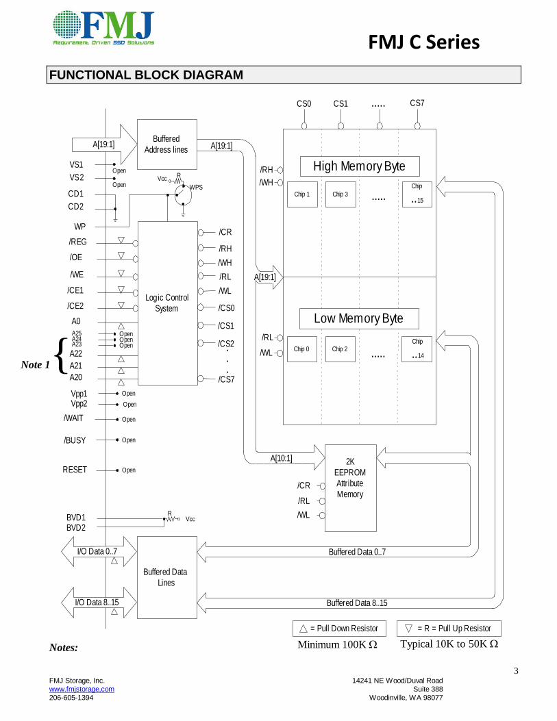
FUNCTIONAL BLOCK DIAGRAM
/RH
/WH
High Memory Byte
CS0 CS1 CS7
Chip 1 Chip 3
Chip
..15
Buffered
Address lines
Logic Control
System
.....
.....
/REG/RH
/WH
/RL
/WL
/CR
/CS2
/CS7
.
.
.
/CS1
/CS0
CD1
CD2
Buffered Data
Lines
Buffered Data 0..7
Buffered Data 8..15
A[19:1]
BVD1BVD2
/BUSY
RESET
/CR
/RL
/WL
2K
EEPROM
Attribute
Memory
A[10:1]
/RL
/WL
Low Memory Byte
Chip 0 Chip 2Chip
..14.....
VS1
VS2
WP
A[19:1]
Open
Open
Vcc
I/O Data 0..7
I/O Data 8..15
A[19:1]
/CE1
/CE2
/OE
/WE
A0
A25
A22
A21
A20
Vpp1 Open
R
Vpp2 Open
/WAIT Open
Vcc
WPS
R
= R = Pull Up Resistor= Pull Down Resistor
Open
Open
OpenOpen
OpenA24A23
Notes:
Note 1{
Minimum 100K Typical 10K to 50K
FMJ C Series
4 FMJ Storage, Inc. 14241 NE Wood/Duval Road
www.fmjstorage,com Suite 388
206-605-1394 Woodinville, WA 98077
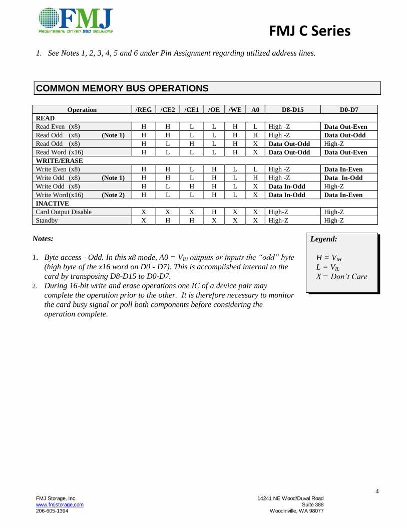
1. See Notes 1, 2, 3, 4, 5 and 6 under Pin Assignment regarding utilized address lines.
COMMON MEMORY BUS OPERATIONS
Operation /REG /CE2 /CE1 /OE /WE A0 D8-D15 D0-D7
READ
Read Even (x8) H H L L H L High -Z Data Out-Even
Read Odd (x8) (Note 1) H H L L H H High -Z Data Out-Odd
Read Odd (x8) H L H L H X Data Out-Odd High-Z
Read Word (x16) H L L L H X Data Out-Odd Data Out-Even
WRITE/ERASE
Write Even (x8) H H L H L L High -Z Data In-Even
Write Odd (x8) (Note 1) H H L H L H High -Z Data In-Odd
Write Odd (x8) H L H H L X Data In-Odd High-Z
Write Word (x16) (Note 2) H L L H L X Data In-Odd Data In-Even
INACTIVE
Card Output Disable X X X H X X High-Z High-Z
Standby X H H X X X High-Z High-Z
Legend:
H = VIH
L = VIL
X = Don’t Care
Notes:
1. Byte access - Odd. In this x8 mode, A0 = VIH outputs or inputs the “odd” byte
(high byte of the x16 word on D0 - D7). This is accomplished internal to the
card by transposing D8-D15 to D0-D7.
2. During 16-bit write and erase operations one IC of a device pair may
complete the operation prior to the other. It is therefore necessary to monitor
the card busy signal or poll both components before considering the
operation complete.
FMJ C Series
5 FMJ Storage, Inc. 14241 NE Wood/Duval Road
www.fmjstorage,com Suite 388
206-605-1394 Woodinville, WA 98077
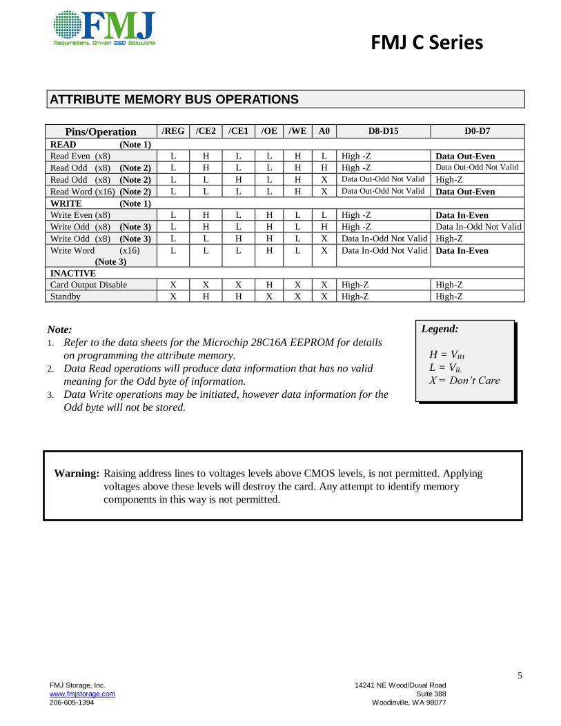
ATTRIBUTE MEMORY BUS OPERATIONS
Pins/Operation /REG /CE2 /CE1 /OE /WE A0 D8-D15 D0-D7
READ (Note 1)
Read Even (x8) L H L L H L High -Z Data Out-Even
Read Odd (x8) (Note 2) L H L L H H High -Z Data Out-Odd Not Valid
Read Odd (x8) (Note 2) L L H L H X Data Out-Odd Not Valid High-Z
Read Word (x16) (Note 2) L L L L H X Data Out-Odd Not Valid Data Out-Even
WRITE (Note 1)
Write Even (x8) L H L H L L High -Z Data In-Even
Write Odd (x8) (Note 3) L H L H L H High -Z Data In-Odd Not Valid
Write Odd (x8) (Note 3) L L H H L X Data In-Odd Not Valid High-Z
Write Word (x16) (Note 3)
L L L H L X Data In-Odd Not Valid Data In-Even
INACTIVE
Card Output Disable X X X H X X High-Z High-Z
Standby X H H X X X High-Z High-Z
Legend:
H = VIH
L = VIL
X = Don’t Care
Note:
1. Refer to the data sheets for the Microchip 28C16A EEPROM for details
on programming the attribute memory.
2. Data Read operations will produce data information that has no valid
meaning for the Odd byte of information.
3. Data Write operations may be initiated, however data information for the
Odd byte will not be stored.
Warning: Raising address lines to voltages levels above CMOS levels, is not permitted. Applying
voltages above these levels will destroy the card. Any attempt to identify memory
components in this way is not permitted.
FMJ C Series
6 FMJ Storage, Inc. 14241 NE Wood/Duval Road
www.fmjstorage,com Suite 388
206-605-1394 Woodinville, WA 98077
PIN DESCRIPTIONS
Vcc
Card Power Supply
Power input required for device operation. The
Vcc must be 5.0 V 5% (4.75V to 5.25V).
GND Card Ground
The VSS pins of all IC components and related
circuitry are connected to this card ground, which
must be connected to the Host system’s ground.
NC
Not Connected
These pins are physically not connected to any
circuitry.
A0-A25 Address Bus
These signals are address input lines that are used
for accesses to card memory. A0 is used to select
the odd or even bank of memory components. A20
through A22 select which Device Pair of ICs will
be accessed. A1 through A19 are used to select
the specific address that is to be accessed on an
individual memory component. A25, A24, and
A23 are Not Connected.
(See also PIN ASSIGNMENTS Notes 1 - 6).
D0-D15 Data (Input/Output) Bus
Data lines D0 through D15 are used to transfer
data to and from the card. When memory is not
selected or outputs are disabled data lines are
placed in a high impedance state.
/OE
Output Enable Signal
This active low input signal enables memory
devices to activate data lines and output data
information.
/WE
Write Enable Signal
This active low input signal controls memory
write functions and is used to strobe data into
the card memory.
WP
Write Protect Signal
This output signal indicates whether or not card
write operations have been disabled by the
Write Protect Switch (WPS). When the signal
is asserted high, card write operations are
disabled. When this signal is asserted low, the
card write operations function normally.
/CE1, /CE2 Card Enable
These are active low inputs used to enable the
card memory. /CE1 accesses the low bank of
memory which provides storage for even
numbered bytes. /CE2 accesses the high bank of
memory which provides storage for odd
numbered bytes. During byte-wide operations
these Card Enable signals are used in
conjunction with address line A0 to access even
or odd bytes of data. The memory card is de-
selected and power consumption is reduced to
standby levels when both /CE1 and /CE2 are
driven high.

FMJ C Series
7 FMJ Storage, Inc. 14241 NE Wood/Duval Road
www.fmjstorage,com Suite 388
206-605-1394 Woodinville, WA 98077
PIN DESCRIPTIONS (CONTINUED)
/REG
Register Select Signal
This active low input signal enables access to the
Attribute memory EEPROM. Attribute memory is
typically used to store the CIS file, which contains
specific card information. Access to common
memory is not possible when /REG is asserted low.
RESET
RESET Signal
This is an active high input signal that normally is
used by the Host to place the card in the deep
power down mode of operation. On these cards
this signal is Not Connected.
/WAIT
Extended Bus Cycle
This active low output signal is used by the card to
delay completion of a memory access operation.
There are no wait states generated by these
memory cards. For this reason the /WAIT signal is
left open. It is the responsibility of the Host to pull
this signal high to prevent false activation.
/BUSY
Ready Busy Signal
This active low output signal normally indicates
that at least one memory device in the card is busy
performing a task. On these cards this signal is Not
Connected.
/CD1, /CD2
Card Detect
These pins are tied directly to ground and are
used by the Host system to detect the presence of
the card. If /CD1 and /CD2 are not both
detected low by the Host, then the card is not
properly inserted.
/VS1, /VS2
Voltage Sense Signals
The Voltage Sense Signals notify the socket of
the card’s Vcc requirements on initial power up.
When both /VS1 and /VS2 are open, as is the
case on these cards, the card is identified to the
Host system as a 5V only card.
/Vpp1, /Vpp2
Program and Peripheral Voltages
These signals are normally used to supply
additional programming voltages for memory
devices that require programming voltages other
than the Vcc supply. This memory card requires
only Vcc voltages. Therefore, Vpp1 and Vpp2
are Not Connected.
/BVD1, /BVD2 Battery Voltage Detect
These pins are normally used to indicate the
status of an internal card battery. Since FLASH
cards do not require or use a battery, these
signals are internally pulled high by a resistor.
FMJ C Series
8 FMJ Storage, Inc. 14241 NE Wood/Duval Road
www.fmjstorage,com Suite 388
206-605-1394 Woodinville, WA 98077
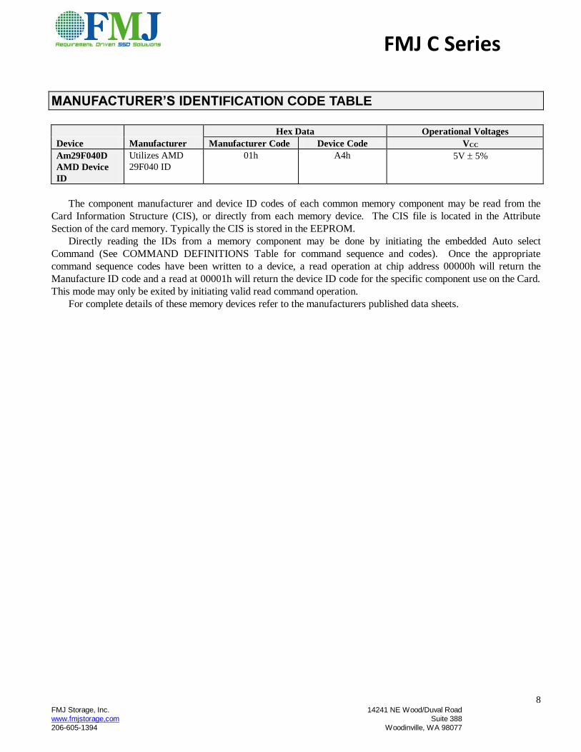
MANUFACTURER’S IDENTIFICATION CODE TABLE
Hex Data Operational Voltages
Device Manufacturer Manufacturer Code Device Code VCC
Am29F040D
AMD Device
ID
Utilizes AMD
29F040 ID
01h A4h 5V 5%
The component manufacturer and device ID codes of each common memory component may be read from the
Card Information Structure (CIS), or directly from each memory device. The CIS file is located in the Attribute
Section of the card memory. Typically the CIS is stored in the EEPROM.
Directly reading the IDs from a memory component may be done by initiating the embedded Auto select
Command (See COMMAND DEFINITIONS Table for command sequence and codes). Once the appropriate
command sequence codes have been written to a device, a read operation at chip address 00000h will return the
Manufacture ID code and a read at 00001h will return the device ID code for the specific component use on the Card.
This mode may only be exited by initiating valid read command operation.
For complete details of these memory devices refer to the manufacturers published data sheets.
FMJ C Series
9 FMJ Storage, Inc. 14241 NE Wood/Duval Road
www.fmjstorage,com Suite 388
206-605-1394 Woodinville, WA 98077
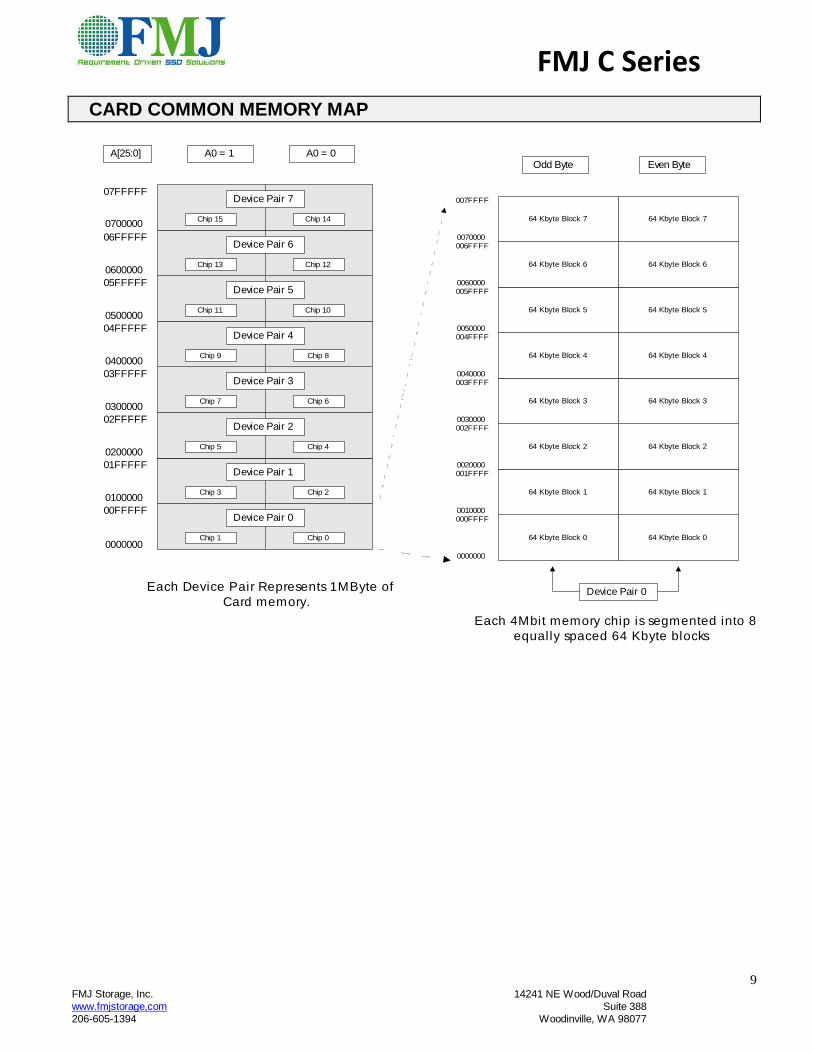
CARD COMMON MEMORY MAP
A[25:0] A0 = 1 A0 = 0
64 Kbyte Block 0 64 Kbyte Block 0
0000000
000FFFF0010000
001FFFF
Device Pair 0
Chip 1 Chip 00000000
01FFFFFDevice Pair 1
Chip 3 Chip 2
0200000
03FFFFF
Device Pair 2
Chip 5 Chip 4
0400000
05FFFFF
Device Pair 3
Chip 7 Chip 6
0600000
07FFFFF
Device Pair 4
Chip 9 Chip 8
Device Pair 5
Chip 11 Chip 10
Device Pair 6
Chip 13 Chip 12
Device Pair 7
Chip 15 Chip 14
Odd Byte Even Byte
Device Pair 0
Each 4Mbit memory chip is segmented into 8
equally spaced 64 Kbyte blocks
64 Kbyte Block 1 64 Kbyte Block 1
64 Kbyte Block 2 64 Kbyte Block 2
64 Kbyte Block 3 64 Kbyte Block 3
64 Kbyte Block 4 64 Kbyte Block 4
64 Kbyte Block 5 64 Kbyte Block 5
64 Kbyte Block 6 64 Kbyte Block 6
64 Kbyte Block 7 64 Kbyte Block 7
0070000
007FFFF
0060000
006FFFF
0040000
004FFFF0050000
005FFFF
0020000
002FFFF0030000
003FFFF
00FFFFF
0100000
02FFFFF
0300000
04FFFFF
0500000
06FFFFF
0700000
Each Device Pair Represents 1MByte of
Card memory.
FMJ C Series
10 FMJ Storage, Inc. 14241 NE Wood/Duval Road
www.fmjstorage,com Suite 388
206-605-1394 Woodinville, WA 98077
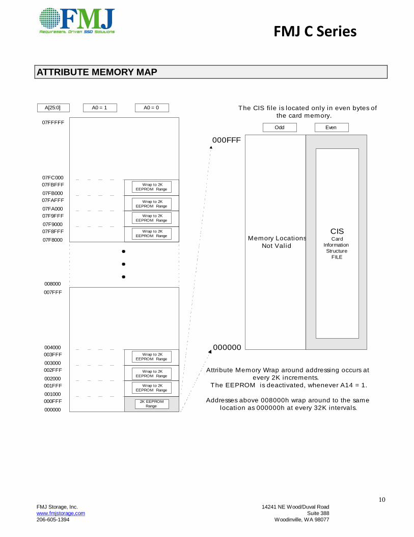
ATTRIBUTE MEMORY MAP
A[25:0] A0 = 1 A0 = 0
Attribute Memory Wrap around addressing occurs at
every 2K increments.
The EEPROM is deactivated, whenever A14 = 1.
Addresses above 008000h wrap around to the same
location as 000000h at every 32K intervals.
Memory Locations
Not Valid
000000
The CIS fi le is located only in even bytes of
the card memory.
000FFF
CISCard
Information
Structure
FILE
008000
000000
000FFF 2K EEPROM
Range
001000
001FFF
002000
002FFF
Wrap to 2K
EEPROM Range
003000
003FFF
Wrap to 2K
EEPROM Range
Wrap to 2K
EEPROM Range
004000
007FFF
Odd Even
07F8000
07F8FFF
07F9000
07F9FFF
07FA000
07FAFFF
Wrap to 2K
EEPROM Range
07FB000
07FBFFF
Wrap to 2K
EEPROM Range
Wrap to 2K
EEPROM Range
07FC000
07FFFFF
Wrap to 2K
EEPROM Range

FMJ C Series
11 FMJ Storage, Inc. 14241 NE Wood/Duval Road
www.fmjstorage,com Suite 388
206-605-1394 Woodinville, WA 98077
COMMAND DEFINITIONS TABLE
All Address and Data values are in Hexadecimal unless otherwise noted. Addresses (Addr) are chip ,not card, addresses.
Embedded
1st Bus Write
Cycle
2nd Bus Write
Cycle
3rd Bus Write
Cycle
4th Bus Write
Cycle
5th Bus Write
Cycle
6th Bus Write
Cycle
Command Bus Addr Data Addr Data Addr Data Addr Data Addr Data Addr Data
Sequence Cyc. Evn Odd Evn Odd Evn Odd Evn Odd Evn Odd Evn Odd
Read/Reset 1* XXXX F0 F0
Read/Reset 4 5555 AA AA 2AAA 55 55 5555 F0 F0 RA RH RL
Autoselect
Manf. ID
4 5555 AA AA 2AAA 55 55 5555 90 90 XX00 01 01
Autoselect
device ID
4 5555 AA AA 2AAA 55 55 5555 90 90 XX01 A4 A4
Word Write 4 5555 AA AA 2AAA 55 55 5555 A0 A0 PA PH PL
Device
Erase
6 5555 AA AA 2AAA 55 55 5555 80 80 5555 AA AA 2AAA 55 55 5555 10 10
Sector
Erase
6 5555 AA AA 2AAA 55 55 5555 80 80 5555 AA AA 2AAA 55 55 SA 30 30
Sector Erase Suspend XXXX B0 B0 Erase can be suspended during sector erase with Addr (don’t care), Data (B0B0h)
Sector Erase Resume XXXX 30 30 Erase can be resumed after suspend with Addr (don’t care), Data (3030h)
Note:
* Operation available after a card power reset, or after write/erase operations have completed.
It should be noted that addresses are latched on the falling edge of the /WE pulse and that data is
latched on the rising edge of /WE (See CARD TIMING CHARACTERISTICS).
Legend:
X = Any valid address with in a
memory device
Write protect must not be enabled for proper command
operations. Address bits A19-A11 are Don’t Care for all
commands except for Read Address (RA), Program
Address (PA), and Sector Address (SA). For any word
operation both the Even and Odd byte device must be
made active through the control line settings. Refer to the
Memory Bus Operations Table for control line settings for
various operation modes.
FMJ C Series
12 FMJ Storage, Inc. 14241 NE Wood/Duval Road
www.fmjstorage,com Suite 388
206-605-1394 Woodinville, WA 98077
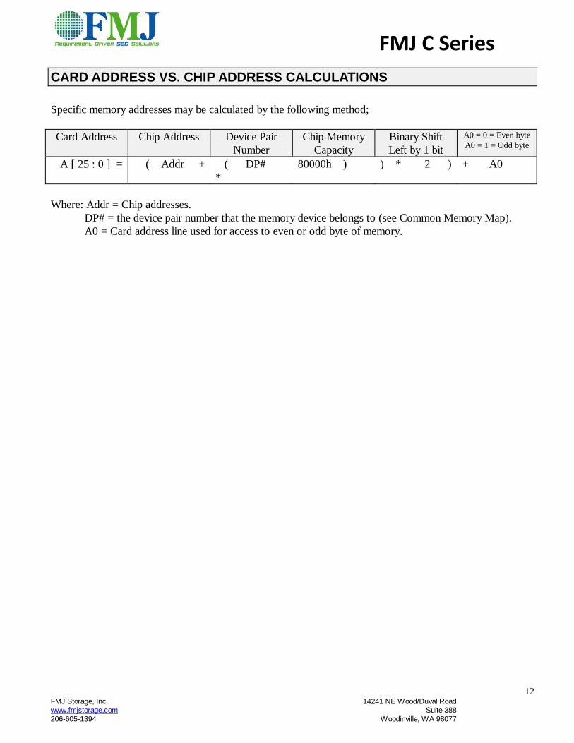
CARD ADDRESS VS. CHIP ADDRESS CALCULATIONS
Specific memory addresses may be calculated by the following method;
Card Address Chip Address Device Pair
Number
Chip Memory
Capacity
Binary Shift
Left by 1 bit
A0 = 0 = Even byte
A0 = 1 = Odd byte
A [ 25 : 0 ] = ( Addr + ( DP#
*
80000h ) ) * 2 ) + A0
Where: Addr = Chip addresses.
DP# = the device pair number that the memory device belongs to (see Common Memory Map).
A0 = Card address line used for access to even or odd byte of memory.

FMJ C Series
13 FMJ Storage, Inc. 14241 NE Wood/Duval Road
www.fmjstorage,com Suite 388
206-605-1394 Woodinville, WA 98077
COMMAND DEFINITIONS TABLE (CONTINUED)
Cards may be read in Byte-Wide or Word-Wide modes. In Word-Wide mode, each byte of memory is
independently read from each device pair. Each memory device in the card may read at different rates.
Therefore, the Host should wait until each byte has a valid data output (See MEMORY BUS
OPERATIONS Table for specific Control line States and CARD TIMING CHARACTERISTICS for
timing information).
Upon power reset of the Card, each memory chip automatically powers up in the Read/Reset state in
order to prevent spurious data changes during power up and does not require an additional Read command
in order to begin reading data from memory at this time. This operation mode can also be initiated by
writing the Read/Reset Command (See Command Definitions Table). The device remains enabled for read
operations until another command is written.
Data reads may also be performed during the Sector Erase Suspend operation. This state is known as
the Pseudo Read state. For further details see Sector Erase Suspend and Data Polling.
During any operation only certain memory devices are active. Those that are not involved in a specific
operation and are not directly made active by control signals can be placed into a reduced power mode by
setting the /CE1 and /CE2 signals to a high logic state. Data output bits are then placed in a high-
impedance state independent of /OE. If a device is deselected during block erase, byte write or lock-bit
operations, the device continues functioning normally until the operation is completed then enters the
Standby Mode ( See MEMORY BUS OPERATIONS Table for specific control line states see also CARD
DC CHARACTERISTICS for the standby current value).
Each chip may be brought out of standby mode and made active by setting the chip enable signals to a
low logic value.
Reset / Read Command:
Standby Mode of Operation:

FMJ C Series
14 FMJ Storage, Inc. 14241 NE Wood/Duval Road
www.fmjstorage,com Suite 388
206-605-1394 Woodinville, WA 98077
COMMAND DEFINITIONS TABLE (CONTINUED)
Upon executing the Embedded Erase command sequence, the addressed memory device automatically
writes and verifies the entire sector(s) for an all “0” data pattern, at which point a self timed chip erase-and-
verify begins. The erase and verify operations are complete when the data on D7 (D15 on the odd byte) of
the memory device is “1”. At which time the device returns to the read mode.
The system is not required to provide any control or timing during these operations. If a power reset
occurs while the erase operation is in progress, the erase operation will stop, and the data in that device will
be undefined. Note that for the device erase or sector erase operation, Data Polling may be performed at
any address in that device or sector (See Polling Operations).
A system designer has the following choices when initiating the Embedded Erase command:
The Host may keep the sector address valid during the entire Embedded Erase operation.
Once the system has initiated the Embedded Erase command sequence, the Host may remove the
address from the device and perform other tasks. (When the Host comes back to poll the device, it
must reassert the same address.)
Embedded Device Erase Command:
Embedded Erase Algorithm Description Table and Diagram:
Start
Write Embedded Erase
Command Sequence
Data Poll Device
Erasure Complete
Bus
Operations
Command Comments
Standby Wait for VCC ramp
Write Embedded Erase
Command sequence
6 Bus Cycle
operations
Read Data Poll to verify
completion

FMJ C Series
15 FMJ Storage, Inc. 14241 NE Wood/Duval Road
www.fmjstorage,com Suite 388
206-605-1394 Woodinville, WA 98077
COMMAND DEFINITIONS TABLE (CONTINUED)
The sequence of six command codes for executing a Sector Erase may be seen in the COMMAND
DEFINITIONS Table. The sector address and the command data are both internally latched on board each
memory device. Sector Erase will begin 100s after the rising edge of the last sector erase command.
During the 100s time-out period, multiple sectors may be queued for concurrent erase. Queuing of
multiple sectors is accomplished by writing the six bus cycle operation commands sequence, followed with
writes of the sector erase command 30h to addresses in other sectors desired to be concurrently erased. The
system is not required to provide any controls or timing during these operations and any command other
than Sector Erase within the time-out window will reset the device to the read mode.
If a power reset occurs after the device has begun executing this command, the erase operation will be
halted and the data in the sector will be undefined. The automatic sector erase terminates when the data on
D7 (D15 on the odd byte) is “1”. Data polling must be performed at an address within any of the sectors
being erased.
Sector Erase Suspend command allows the Host to interrupt the erase operation of the chip and then do
data reads (pseudo-read) from a non-busy sector. The chip will take between 0.1s to 10s to suspend the
erase operation and go into erase suspended read mode.
This mode is only available during the Sector Erase operation and will be ignored during other
command operations. Writing this command during the Sector Erase 100s time-out period will result in
immediate suspension of the Sector Erase operation.
Once the device has entered the Sector Erase Suspend mode, any further writes of the command (B0h)
at this time will be ignored. Any attempt to initiate other commands during the Erase Suspend mode
window will reset the device to read mode. In order to resume the Sector Erase operation, the Resume
command (30h) should be written to the suspended device.
Note that the Host system must keep track of what state the chip is in by monitoring D6 (D14 on the
odd byte) to determine if a chip has entered the pseudo-read mode
(See Polling Operations for Toggle Bit D6).
Sector Erase Command:
Sector Erase Suspend/Resume:

FMJ C Series
16 FMJ Storage, Inc. 14241 NE Wood/Duval Road
www.fmjstorage,com Suite 388
206-605-1394 Woodinville, WA 98077
COMMAND DEFINITIONS TABLE (CONTINUED)
The Embedded Program setup consists of four command codes (See COMMAND DEFINITIONS
TABLE). Once the Embedded Program commands are written the next /WE pulse causes a transition to an
active programming operation (See CARD TIMING CHARACTERISTICS). The Host system is not
required to provide further control timing the device will automatically provide an adequate internally
generated write pulse and verify margin.
When the automatic programming operation is completed, the device returns to the Read mode and the
data on D7 (D15 on the odd byte) is equivalent to the data written.
In Word-Wide mode, each byte is independently programmed on each memory device pair. Because
each device may reach completion of the programming operation at different times, software polling should
continue to monitor each byte for write completion and data verification.
A system designer has the following choices when initiating the Embedded Programming command:
The Host may keep the address valid during the entire Embedded Programming operation.
Once the system has initiated the Embedded Program command sequence, the Host may remove the
address from the device and perform other tasks. (When the Host comes back to poll the device, it
must reassert the same address.)
Start
Write Embedded Write
Command Sequence
Data Poll Device
Write Complete
Verify
Data
Last
Address
increment
Address
Yes
Yes
No
No
Embedded Program Command:
Embedded Program Algorithm Description Table and Flow Chart:
Bus
Operations
Command Comments
Standby Wait for Vcc ramp
Write Embedded Program
Command sequence
3 bus cycle operation
Write Program
Address/Data
1 bus cycle operation
Read Data Poll to verify
completion
FMJ C Series
17 FMJ Storage, Inc. 14241 NE Wood/Duval Road
www.fmjstorage,com Suite 388
206-605-1394 Woodinville, WA 98077
COMMAND DEFINITIONS TABLE (CONTINUED)
Polling is a method to indicate to the Host system that the Embedded algorithms are either in progress or complete
and these is only active during the Embedded Programming or Erase modes of operation.
Data Polling Bit D7 (D15 on the odd byte) During an embedded programming cycle, any attempt to read from a device will produce the complement of
expected valid data on D7. While an embedded erase cycle is being performed, D7 (D15 on the odd byte) will read
“0” until the erase is completed. Upon completion of the erase operation the data on D7 (D15 on the odd byte) will
read “1”.
Even if D7 that the device has completed the embedded operation, the other data bits of the byte D0-D6 may still
be invalid since the switching time for each data bit will not be the same. The valid data will be provided only after a
certain time delay (> tGLQV) (See CARD TIMING CHARACTERISTICS).
Toggle Bit D6 (D14 on the odd byte) During an Embedded Program/Erase Algorithm cycle, successive attempts to read (/OE toggling) data from the
device at any address will result in D6 (D14 on the odd byte) toggling between logical one and zero. Once the
Embedded Program/Erase Algorithm cycle is complete, D6 (D14 on the odd byte) will stop toggling and valid data
will be read on the next successive attempt. (See Command Status Flags Table)
Time Limit Exceeded Bit D5 (D13 on the odd byte) Time Limit Exceeded indicates a failure of the performed operation, and is identified by the D5 bit set to logical
one.
Notes:
Start
FAIL PASS
D7 = Data?
Yes
No
Yes
No
No
Yes
D5 = 1?
D7 = Data?
Read Byte at Valid
Address
Read Byte at Valid
Address
Polling Operations:
Data Polling Algorithm: Toggle Bit Algorithm:
Start
FAIL PASS
D6 =
Toggle?
Yes
No
Yes
No
No
Yes
D5 = 1?
D6 =
Toggle?
Read Byte at Valid
Address
Read Byte at Valid
Address

FMJ C Series
18 FMJ Storage, Inc. 14241 NE Wood/Duval Road
www.fmjstorage,com Suite 388
206-605-1394 Woodinville, WA 98077
1. D7 is rechecked if D5 = 1 because D7 may change simultaneously with D5.
2. D6 is rechecked if D5 = 1 because D7 may change simultaneously with D5
3. Bits D7, D6, and D5 correspond to bit D15, D14, and D13 on the odd byte respectively.
FMJ C Series
19 FMJ Storage, Inc. 14241 NE Wood/Duval Road
www.fmjstorage,com Suite 388
206-605-1394 Woodinville, WA 98077
COMMAND DEFINITIONS TABLE (CONTINUED)
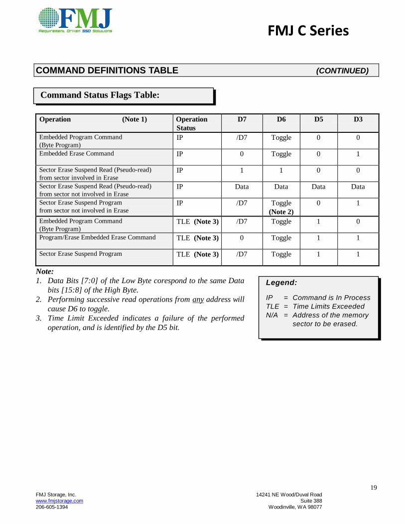
Operation (Note 1) Operation
Status
D7 D6 D5 D3
Embedded Program Command
(Byte Program) IP /D7 Toggle 0 0
Embedded Erase Command
IP 0 Toggle 0 1
Sector Erase Suspend Read (Pseudo-read)
from sector involved in Erase IP 1 1 0 0
Sector Erase Suspend Read (Pseudo-read)
from sector not involved in Erase IP Data Data Data Data
Sector Erase Suspend Program
from sector not involved in Erase IP /D7 Toggle
(Note 2)
0 1
Embedded Program Command
(Byte Program) TLE (Note 3) /D7 Toggle 1 0
Program/Erase Embedded Erase Command
TLE (Note 3) 0 Toggle 1 1
Sector Erase Suspend Program
TLE (Note 3) /D7 Toggle 1 1
Note:
1. Data Bits [7:0] of the Low Byte corespond to the same Data
bits [15:8] of the High Byte.
2. Performing successive read operations from any address will
cause D6 to toggle.
3. Time Limit Exceeded indicates a failure of the performed
operation, and is identified by the D5 bit.
Legend:
IP = Command is In Process
TLE = Time Limits Exceeded
N/A = Address of the memory
sector to be erased.
Command Status Flags Table:

FMJ C Series
20 FMJ Storage, Inc. 14241 NE Wood/Duval Road
www.fmjstorage,com Suite 388
206-605-1394 Woodinville, WA 98077
CARD TIMING CHARACTERISTICS
(Standard operating times for both Common and Attribute Memory unless otherwise noted.)
Read Cycle Timing (/WE = VHI)
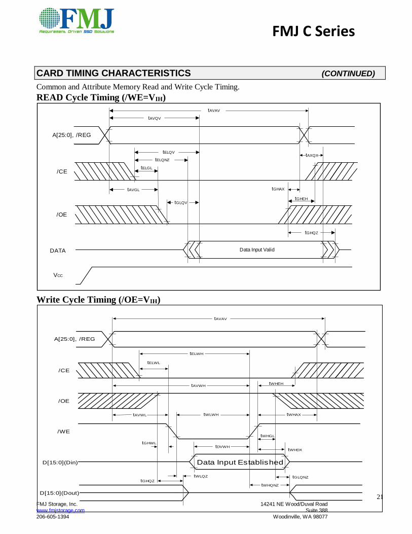
Parameter Symbol Min Max Units
Read Cycle Time tAVAV 200 ns
Address Access Time tAVQV 200 ns
Card Enable Access Time tELQV 200 ns
Output Enable Access Time tGLQV 125 ns
/OE High to Data Output Disable tGHQZ 90 ns
/CE Low to Data Output Enable tELQNZ 5 ns
Address change to Data no longer valid tAXQX 0 ns
Address Setup to /OE Low time tAVGL 20 ns
/OE High Setup to Address time tGHAX 20 ns
/CE Low Setup to /OE Low time tELGL 0 ns
/OE High to /CE High Hold time tGHEH 20 ns
Write Cycle Timing (/OE = VHI)
Parameter Symbol Min Max Units
Write Cycle Time tAVAV 200 ns
Write Pulse Width tWLWH 120 ns
Address Setup Time for /WE Low tAVWL 20 ns
Address Setup to /WE High tAVWH 140 ns
Card Enable Setup to /WE Low tELWH 140 ns
Data Setup to /WE High tDVWH 60 ns
Data Hold from /WE High tWHDX 30 ns
Address Hold from /WE High tWHAX 30 ns
Data Output Disable Time form /WE Low tWLQZ 90 ns
Data Output Disable Time form /OE Low tGHQZ 90 ns
/WE High time to Data Output Enable tWHQNZ 5 ns
/OE Low time to Data Output Enable tGLQNZ 5 ns
/OE High to /WE Low Setup time tGHWL 10 ns
/WE High to /OE Low Hold time tWHGL 10 ns
/CE Low to /WE Low Setup time tELWL 0 ns
/WE High to /CE High Hold time tWHEH 20 ns
FMJ C Series
21 FMJ Storage, Inc. 14241 NE Wood/Duval Road
www.fmjstorage,com Suite 388
206-605-1394 Woodinville, WA 98077
CARD TIMING CHARACTERISTICS (CONTINUED)
Common and Attribute Memory Read and Write Cycle Timing.
READ Cycle Timing (/WE=VIH)
Write Cycle Timing (/OE=VIH)
A[25:0], /REG
/CE
/OE
/WE
D[15:0](Din)
D[15:0](Dout)
tAVAV
tELWH
tELWL
tAVWHtWHEH
tAVWL tWLWH tWHAX
tGHWL
tWLQZ
tGHQZ
tWHQNZ
tDVWH
tWHGL
tWHDX
tGLQNZ
Data Input Established
A[25:0], /REG
/CE
/OE
DATA
tAVAV
tAVQV
Data Input Valid
tELQV
tGLQV
tAXQX
tGHQZ
tGHAX
tELGL
tAVGL
tGHEH
VCC
tELQNZ
FMJ C Series
22 FMJ Storage, Inc. 14241 NE Wood/Duval Road
www.fmjstorage,com Suite 388
206-605-1394 Woodinville, WA 98077
CARD TIMING CHARACTERISTICS (NOTE 1) (CONTINUED)
WRITE OPERATIONS AND DATA POLLING TIMING DIAGRAM
/WE controlled write timings and data polling.
Item Symbol Min Typ Max Units
Power (VCC) High Recovery to /CE Going Low tPHEL 50 s
Write Pulse Width tWLWH 80 ns
Write Pulse Width Hold High tWPH 85 ns
Chip Embedded Program Operations tWHWH 16 s
48 ms
VCC
Program Setup
Commands
Data Poll Data Bit 7 Set up for Read Data
Command
Data InData In /D7 Bit
Data Out
Valid
A[25:0]
/CE
/OE
/WE
Data
VIL
VIH
VOL
VOH
VIL
VIH
VIL
VIH
VIL
VIH
VIL
VIH
tWHWH
tWLWH
tWPH
tPHEL
Address location to be
Programmed
Address location that
was Programmed
Address location that
was Programmed
FMJ C Series
23 FMJ Storage, Inc. 14241 NE Wood/Duval Road
www.fmjstorage,com Suite 388
206-605-1394 Woodinville, WA 98077
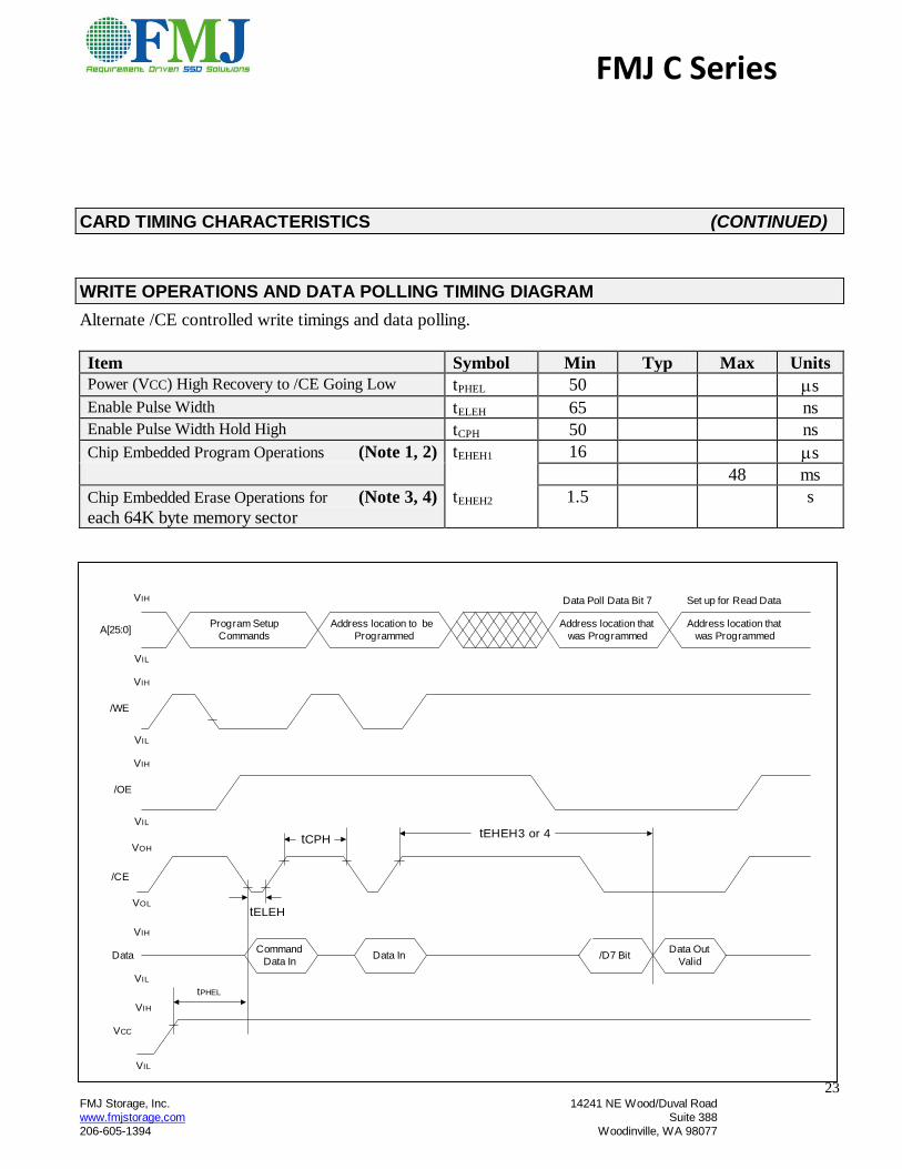
CARD TIMING CHARACTERISTICS (CONTINUED)
WRITE OPERATIONS AND DATA POLLING TIMING DIAGRAM
Alternate /CE controlled write timings and data polling.
Item Symbol Min Typ Max Units
Power (VCC) High Recovery to /CE Going Low tPHEL 50 s
Enable Pulse Width tELEH 65 ns
Enable Pulse Width Hold High tCPH 50 ns
Chip Embedded Program Operations (Note 1, 2) tEHEH1 16 s
48 ms
Chip Embedded Erase Operations for (Note 3, 4)
each 64K byte memory sector
tEHEH2 1.5 s
VCC
Program Setup
Commands
Data Poll Data Bit 7 Set up for Read Data
Command
Data InData In /D7 Bit
Data Out
Valid
A[25:0]
/WE
/OE
/CE
Data
VIL
VIH
VOL
VOH
VIL
VIH
VIL
VIH
VIL
VIH
VIL
VIH
tEHEH3 or 4
tELEH
tCPH
tPHEL
Address location to be
Programmed
Address location that
was Programmed
Address location that
was Programmed
FMJ C Series
24 FMJ Storage, Inc. 14241 NE Wood/Duval Road
www.fmjstorage,com Suite 388
206-605-1394 Woodinville, WA 98077
CARD TIMING CHARACTERISTICS (CONTINUED)
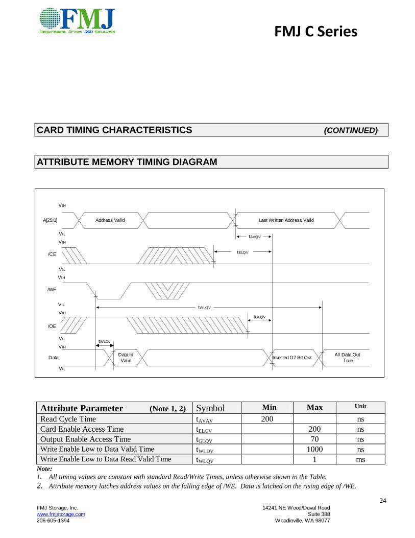
ATTRIBUTE MEMORY TIMING DIAGRAM
Attribute Parameter (Note 1, 2) Symbol Min Max Unit
Read Cycle Time tAVAV 200 ns
Card Enable Access Time tELQV 200 ns
Output Enable Access Time tGLQV 70 ns
Write Enable Low to Data Valid Time tWLDV 1000 ns
Write Enable Low to Data Read Valid Time tWLQV 1 ms Note:
1. All timing values are constant with standard Read/Write Times, unless otherwise shown in the Table.
2. Attribute memory latches address values on the falling edge of /WE. Data is latched on the rising edge of /WE.
Data In
Valid
All Data Out
TrueData
VIL
VIH
Inverted D7 Bit Out
/CE
VIL
VIH
A[25:0]
VIL
VIH
Address Valid Last Written Address Valid
tELQV
tAVQV
tGLQV
tWLDV
/OE
VIL
VIH
tWLQV
/WE
VIL
VIH

FMJ C Series
25 FMJ Storage, Inc. 14241 NE Wood/Duval Road
www.fmjstorage,com Suite 388
206-605-1394 Woodinville, WA 98077
Data Polling, the 28C16A features /DATA polling to signal the completion of a byte write cycle. During a
write cycle, an attempt to read the last byte written to memory will produce the complement of the D7 (D6
to D0 are indeterminate). After completion the true data is available. Data Polling allows a simple
read/compare operation to determine the status of the chip.
RECOMMENDED OPERATING CONDITIONS
Rating Symbol Min. Max. Units
Vcc Supply Voltage Vcc 4.75 5.25 V
Operating Temperature TA -10 70 C
DC CHARACTERISTICS
Supply current is an RMS value. Typical values at nominal VCC voltage at TA = +25°C. Symbol Parameter Condition Min Max Units
ICCS Standby Current
(Note 2)
Per device:
CMOS; VCC = VCC Max , VIN = GND to VCC
/CE1, /CE2, = VCC 0.2V
0.7 mA
ICCR Active Read Current
(Note 1, 2)
CMOS; VCC = VCC Max
/CE1 or /CE2 = GND Byte (8) 45 mA
IOUT = 0mA, at f = 3.3MHZ
Byte (16) 90 mA
ICCW Active Program Current
(Note 1, 3)
Per device: /CE1 or /CE2 = GND
( including programming current ) 65 mA
ICCE Active Sector Erase
Current (Note 3)
Per device:
( including programming current ) 50 mA
IIL Input Leakage Current
VIN = GND to VCC, VCC MAX
Per Pin: -300 +20 A
IILpu Input Leakage Current
with Pull Up Resistor
VIN = GND to VCC, VCC MAX
Per Pin with 10K pull up resistor +500 A
IILpd Input Leakage Current
with Pull Down Resistor
VIN = GND to VCC, VCC MAX
Per Pin with 100K pull down resistor -50 A
IOLpd Output Leakage Current
with Pull Down Resistor
VOUT = GND to VCC, VCC MAX
Per Pin with 100K pull down resistor 20 A
VIL Input Low Voltage
(Note 3)
-0.5 0.8 V
VIH Input High Voltage
(Note 3)
0.7 VCC VCC +0.3 V
VOL Output Low Voltage
(Note 3)
VCC = VCC Min
IOL = 3.22 mA 0.40 V
VOH Output High Voltage
(Note 3)
CMOS; VCC = VCC Min 3.8 VCC V
Attribute Data Polling Mode:

FMJ C Series
26 FMJ Storage, Inc. 14241 NE Wood/Duval Road
www.fmjstorage,com Suite 388
206-605-1394 Woodinville, WA 98077
Iout = 2.0 mA
VLKO Low VCC (Lock-Out ) 3.2 4.2 V
Notes: 1. ICCWS and ICCES are specified with the device deselected. If read or written while in erase suspend mode, the
device’s current is the sum of ICCWS or ICCWS and ICCR or ICCW.
2. CMOS inputs are either VCC 0.2V or GND 0.2V.
3. Sample tested by component manufacturer.
CARD INFORMATION STRUCTURE
The CIS is data which describes the PCMCIA card and is described by the PCMCIA standard. This
information can be used by the Host system to determine a number of things about the card that has been
inserted. For information regarding the exact nature of this data, and how to design Host software to
interpret it, refer to the PCMCIA standard Metaformat Specification.
Physical Logical Data Tuple
Address Address Value(s) Description
00h 00h 01h CISTPL_DEVICE 02h 01h 03h CISTPL_LINK 04h 02h 52h Speed = 200ns, WPS=Yes, FLASH 06h 03h 1Eh (Note 1) Bits 2-0 = 110b = 2 Meg units,
Bits 7-3 = 00011b = 4 Units (0=1, 1=2...)
2 Meg x 4 = 8 Meg size 08h 04h FFh CISTPL_END - End of Tuple
0Ah 05h 18h CISTPL_JEDEC 0Ch 06h 03h CISTPL_LINK 0Eh 07h 89h Manufacturer ID (AMD) 10h 08h A6h Device ID (Am29F040) 12h 09h FFh CISTPL_END - End of Tuple
14h 0Ah 1Eh CISTPL_DEVICEGEO 16h 0Bh 07h CISTPL_LINK 18h 0Ch 02h DGTPL_BUS - Bus Width - 2 Bytes 1Ah 0Dh 11h DGTPL_EBS - Erase Block Size
2^10h = 64K Bytes or Words 1Ch 0Eh 01h DGTPL_RBS - Byte Accessible 1Eh 0Fh 01h DGTPL_WBS - Byte Accessible 20h 10h 01h DGTPL_PART - One Partition 22h 11h 01h DGTPL_HWIL - No Interleave 24h 12h FFh CISTPL_END - End of Tuple
Note:
1. Refer to the table (right) for FMJ Storage part umbers and corresponding data value.

FMJ C Series
27 FMJ Storage, Inc. 14241 NE Wood/Duval Road
www.fmjstorage,com Suite 388
206-605-1394 Woodinville, WA 98077
CARD INFORMATION STRUCTURE (CONTINUED
Physical Logical Data Tuple
Address Address Value(s) Description
26h 13h 15h CISTPL_VERS1 28h 14h 54h CISTPL_LINK 2Ah 15h 04h TPLLV1_MAJOR (PCMCIA 2.1/JEIDA 4.2) 2Ch 16h 01h TPLLV1_MINOR 2Eh...66h 17h...33h 46 4d 4a 20
53 74 6f 72
61 67 65 2c
20 49 6e 63
2e 0d 0a
ASCII Text is :
FMJ Storage, Inc.
{19 Characters total}
68h 34h 00 NULL String Delimiter (String 1) 6Ah...84h 35h...42h 4c 46 4c 2d
38 4d 42 2d
31 35 43 2d
31 53 30 30
ASCII Text is : (Note 2)
LFL-8MB-15C-1S00
{16 Characters total}
86h 43h 00 NULL String Delimiter (String 2) 88h...CAh 44h...65h 30 38 20 4D
45 47 20 46
4C 41 53 48
20 20 20 20
20 20 20 20
20 20 20 20
20 20 20 20
20 20 20 20
20 20
ASCII Text is : (Note 3)
08 MEG FLASH
{34 Characters total}
CCh 66h 00 NULL String Delimiter (String 3) CEh 67h 00 NULL String Delimiter (String 4) D0h 68h FF CISTPL_END - End of Tuple
D2h 69h FF CISTPL_END - End of Chain Tuple
Notes:
2. Specific Product description will be listed (See Note 1 Part Numbers).
3. Specific Product memory capacities will be listed for specific products.

FMJ C Series
28 FMJ Storage, Inc. 14241 NE Wood/Duval Road
www.fmjstorage,com Suite 388
206-605-1394 Woodinville, WA 98077
5.0 Ordering Information The following describes the part number ordering nomenclature from FMJ Storage.
LFC-02MB-15C-1S00
Form Factor = Linear PC
Vendor/Customer Specific
Capacity 01M – 1 Megabytes
02M – 2 Megabytes
04M – 4 Megabytes
08M – 8 Megabytes
Speed 15/20 ns
Temp. Range C (0 to 70C) I (-40 to 85C)
Vendor/Customer Specific 1st Digit = Attribute Memory 0 = without attribute memory 1 = with attribute memory 2ND Digit = Vendor Specific 3rd Digit = Write Protect 0 = without write protect 1 = with write protect 4th Digit = AMD series 1 = C series 2 = D series

FMJ C Series
29 FMJ Storage, Inc. 14241 NE Wood/Duval Road
www.fmjstorage,com Suite 388
206-605-1394 Woodinville, WA 98077
Available In Type II PCMCIA only
Copyright 2013, FMJ Storage Inc. All Rights Reserved
AMD is a registered trademark of AMD Corporation. All other trademarks, registered trademarks, and service marks are the
property of their respective owners.
The information contained in this document has been carefully checked and is believed to be reliable. However, FMJ Storage
Inc. assumes no responsibilities for inaccuracies.
The information contained in this document does not convey any license under the copyrights, patent rights or trademarks
claimed and owned by FMJ Storage Technologies, Inc.
FMJ Storage, Inc. reserves the right to change products or specifications without notice.
No part of this publication may be copied or reproduced in any form or by any means, or transferred to any third party without
prior written consent of FMJ Storage, Inc.
Week
(1-52) Year
CTI Lot #