FM25Q32 · 2015-12-11 · FM25Q32 is offered in an 8-pin plastic 208-mil width VSOP, 8-pin plastic...
64
Rev.06 (May.20.2011) 1 FM25Q32 FM25Q32 32M-BIT Serial Flash Memory with 4KB Sectors, Dual and Quad I/O SPI
Transcript of FM25Q32 · 2015-12-11 · FM25Q32 is offered in an 8-pin plastic 208-mil width VSOP, 8-pin plastic...

Rev.06 (May.20.2011) 1
FM25Q32
FM25Q32
32M-BIT Serial Flash Memory with 4KB Sectors, Dual and Quad I/O SPI

Rev.06 (May.20.2011) 2
FM25Q32
Documents title
32M bit Serial Flash Memory with 4KB Sectors, Dual and Quad I/O SPI
Revision History
Revision
No.
History Draft date Remark
0.0 Initial Draft Apr.2010 preliminary
0.1 Flash Part Numbering System Jul.2010 preliminary
0.2
Write Status Register (01h)
previous bits => cleared to 0 Change
Read instructions tSHSL20ns => 10ns Change
Aug.18.2010 preliminary
0.3 Add Read SFDP (5Ah) Dec.02.2010 final
0.4 Revised ICC2/ICC4 Dec.24.2010 final
0.5
Add Dual/Quad output fast read
Add SFDP definition table
Revised Part Numbering System
Jan.13.2011 final
0.6 Add VSOP
Modified some descriptions May.20.2011 Final

Rev.06 (May.20.2011) 3
FM25Q32
Table of Contents 1. FEATURES……………………………………….……………………………………..……………………5
2. GENERAL DESCRIPTION……………………….………………………………………………………....5
3. PIN / PAD CONFIGURATION………………….…………………………………………………………...6
3.1 8-Pin SOIC 208-MIL / VSOP 208-MIL…………………………………….………………….6
3.2 8-Pad WSON 6X5-MM……………………………………………………..………………….6
3.3 8-Pin PDIP 300-MIL…………………………………………………………………………….6
3.4 16-Pin SOIC 300-MIL………………………………………………………………………..…7
4. PIN / PAD DESCRIPTION………………………………………………………………………..………….8
4.1 SOIC 208-MIL, VSOP 208-MIL, WSON 6X5-MM, PDIP 300-MIL………….……………..8
4.2 SOIC 300-MIL………………………………………………………..........……….…………..8
4.3 Package Type…………………………………………………………………………..……….8
5. SIGNAL DESCRIPTION……………………………………………………………………………………..9
5.1 Chip Select (/CS)……………………………………….………………………………………9
5.2 Serial Data Input, Output and IOs (DI, DO and IO0, IO1, IO2, IO3)………………………9
5.3 Write Protect (/WP)…………………………………………….……….……….……….…….9
5.4 HOLD (/HOLD)…………………………………………………………………….……………9
5.5 Serial Clock (CLK)…………………………………………………………..………….………9
6. BLOCK DIAGRAM…………………………………………………………………….…………………….10
7. FUNCTIONAL DESCRIPTION…………………………………………………..………………………..11
7.1 Standard SPI Instructions………………………………………..………….………………..11
7.2 Dual SPI Instructions…………………………………….……………………………………11
7.3 Quad SPI Instructions……………………………………………….……..…………………11
7.4 Hold Function………………………………………………………………………………….11
8. WRITE PROTECTION…………………………………………………………….….……..……………..12
8.1 Write protect Features………………………………………………………………..………12
9. STATUS REGISTER………………………………………………………………….…………………….13
9.1 BUSY………………………………………………………………………..………………….14
9.2 Write Enable Latch (WEL)……………………………………………………………………14
9.3 Block Protect Bits (BP2, BP1, BP0)…………………………………………………………14
9.4 Top/Bottom Block protect (TB)……………………………………….………………………14
9.5 Sector/Block Protect (SEC)…………………………………………………………………..14
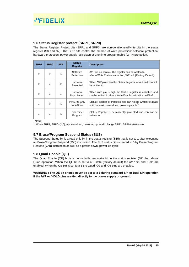
9.6 Status Register protect (SRP1, SRP0)…………………………………….……………….15
9.7 Erase/Program Suspend Status (SUS)……………………………..………………………15
9.8 Quad Enable (QE)……………………………………………………................…………..15
9.9 Status Register Memory Protection…………………………………………………………16
10. INSTRUCTIONS…………………………………………………………………………………………….17
10.1 Manufacturer and Device Identification………………………………….………………….17
10.2 Instruction Set Table 1……………………………………………….……………………….18
10.3 Instruction Set Table 2………………………………………………………………………..19
10.4 Write Enable (06h)…………………………………….………………………………………20
10.5 Write Enable for Volatile Status Register (50h)…………………………………………….20
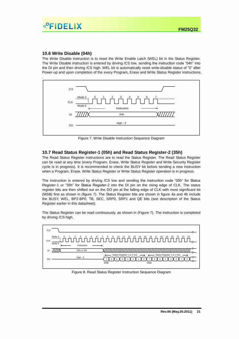
10.6 Write Disable (04h)……………………………………………………………………………21
10.7 Read Status Register-1 (05h) and Read Status Register-2 (35h)…………………….…21
10.8 Write Status Register (01h)…………………………………………………………………..22
10.9 Read Data (03h)……………………………………………………..……………………….23
10.10 Fast Read (0Bh)……………………………………………………………...……………….23
10.11 Fast Read Dual Output (3Bh)……………………………………………….………….……24
10.12 Fast Read Quad Output (6Bh)……………………………………………………………….25
10.13 Fast Read Dual I/O (BBh)…………………………………………..……………………….26
10.14 Fast Read Quad I/O (EBh)……………………………………..……………………………28
10.15 Page Program (02h)…………………………………………………………………………..39
10.16 Quad Data Input Page Program (32h)...........................................................................30
10.17 Quad Data Page Program (38h)………………………………….…………………………31
10.18 Sector Erase (20h).........................................................................................................32
Rev.06 (May.20.2011) 4
FM25Q32
10.19 32KB Block Erase (52h)………………………………….…………………………………..33
10.20 64KB Block Erase (D8h)……………………………….…………………………………….34
10.21 Chip Erase (C7h / 60h)……………………………………………………………………….35
10.22 Erase / Program Suspend (75h)……….……………………………………………………36
10.23 Erase / Program Resume (7Ah)………………………………….………………………….37
10.24 Deep Power-down (B9h)……………………………..……………………………………..38
10.25 Release Deep Power-down / Device ID (ABh)………………………………..…………..39
10.26 Read Manufacturer/ Device ID (90h),(EFh),(DFh)…………………..…………………….40
10.27 JEDEC ID (9Fh)……………………………………………………………………………….42
10.28 Read Serial Flash Discovery Parameter(5Ah)………………..........................………….43
10.29 Mode Bit Reset (FFh)…………………………………………………………………………46
10.30 Enter Secured OTP (B1h)……………………………………………………………………46
10.31 Exit Secured OTP (C1h)………………………………………….…………………………..47
10.32 Read Security Register (2Bh)………………………………………………….…………….47
10.33 Write Security Register (2Fh)…………………….………………………………………….48
10.34 Set Burst with Wrap (77h)……………………………………………………………………49
11. 4K-bit Secured OTP………………………………………………………………….……………………..50
12. ELECTRICAL CHARACTERISTICS………………………………………………………………………51
12.1 Absolute Maximum Ratings………………………………………………………………….51
12.2 Operating Ranges…………………………………………………….………………………51
12.3 Endurance and Data Retention……………………………………….……………………..52
12.4 Power-up Timing and Write Inhibit Threshold…………………………..………………….52
12.5 DC Electrical Characteristics…………………………………………..……………………53
12.6 AC Measurement Conditions…………………………………….…………………………..54
12.7 AC Electrical Characteristics…………………………………………………………………55
12.8 AC Electrical Characteristics (cont’d)……………………………………………………….56
12.9 Serial Output Timing…………………………………………………………..………………57
12.10 Input Timing……………………………………………………..……………………………..57
12.11 Hold Timing………………………………………………………………………..…………..57
13. PACKAGE SPECIFICATION………………………………………………………………………………58
13.1 8-Pin SOIC 208-mil……………………………………………………………………………58
13.2 8-Pin VSOP 208-mil …………………………………….……………………………………59
13.3 8-Pin PDIP 300-mil……………………………………………………………………………60
13.4 8-contact 6x5 WSON…………………………………..……………………………………..61
13.5 8-contact 6x5 WSON Cont’d…………………………………..…………………………….62
13.6 16-Pin SOIC 300-mil………………………………………………………………………….63
14. ORDERING INFORMATION…………………………………….…………………………………………64

Rev.06 (May.20.2011) 5
FM25Q32
1. FEATURES
■ SPI Flash Memory
-32M-bit / 4M–byte Serial Flash
-256-bytes per programmable page
-4K-bit secured OTP
■ Standard, Dual or Quad SPI
-Standard SPI: CLK, /CS, DI, DO, /WP, /Hold
-Dual SPI: CLK, /CS, IO0, IO 1, /WP, /Hold
-Quad SPI: CLK, /CS, IO0, IO1, IO2, IO3
■ High Performance
-104MHz clock operation
-208MHz equivalent Dual SPI
-416MHz equivalent Quad SPI
-50MB/S continuous data transfer rate
-31MB/S random access (32-byte fetch)
-Comparable to X16 Parallel Flash
■ Flexible Architecture
-Uniform Sector Erase (4K-byte)
-Block Erase (32K and 64K-bytes)
-Erase/Program Suspend & Resume
■ Endurance
-100K program/ erase cycles
■ Low Power Consumption
-Single 2.7 to 3.6V supply
-5mA active current
-<3μA Deep Power-down (typ.)
■ wide Temperature Range
--40℃ to +85℃ operating range
■ Advanced Security Features
-Software and Hardware Write-protect
-Top or Bottom, Sector or Block selection
-Lock-Down and OTP protection
■ Package Options
-8-pin SOIC 208-mil
-8-pad WSON 6x5-mm
-16-pin SOIC 300-mil
-8-pin DIP 300-mil
-8-pin VSOP 208-mil
■ Package Material
-Fidelix all product Green package
Lead-free & Halogen-free
RoHS Compliant
2. GENERAL DESCRIPTION
The FM25Q32 SPI flash supports the standard Serial peripheral Interface (SPI), and supports the
Dual/Quad SPI: Serial Clock, Chip Select, Serial Data I/O0(DI), I/O1(DO), I/O2(/WP), and
I/O3(/HOLD).
SPI clock frequencies of up to 104MHz are supported allowing equivalent clock rates of 208MHz
for Dual Output and 416MHz for Quad Output when using the Fast Read Dual/Quad I/O
instructions. These transfer rates are comparable to those of 8 and 16-bit Parallel Flash memories.
The FM25Q32 array is organized into 16.384 programmable pages of 256-bytes each. Up to 256
bytes can be programmed at a time using the Page Program instructions. Pages can be erased
Sector, 32KB Block, 64KB Block or the entire chip.
The devices operate on a single 2.7V to 3.6V power supply with current consumption as low as
5mA active and 3μA for Deep Power-down. All devices offered in space-saving packages. The
device supports JEDEC standard manufacturer and device identification with a 4K-bit Secured
OTP.

Rev.06 (May.20.2011) 6
FM25Q32
3. PIN / PAD CONFIGURATION
3.1 8-Pin SOIC 208-MIL / VSOP 208-MIL
VCC
DI(IO0)
CLK
/HOLD(IO3)
/CS
GND
/WP(IO2)
DO(IO1)
1 8
7
6
54
3
2
VCC
DI(IO0)
CLK
/HOLD(IO3)
/CS
GND
/WP(IO2)
DO(IO1)
1 8
7
6
54
3
2
Figure 1a. Pin Assignments, 8-pin SOIC 208-mil / VSOP 208-mil
3.2 8-Pad WSON 6X5-MM
VCC
DI(IO0)
CLK
/HOLD(IO3)
/CS
GND
/WP(IO2)
DO(IO1)
1 8
7
6
54
3
2
VCC
DI(IO0)
CLK
/HOLD(IO3)
/CS
GND
/WP(IO2)
DO(IO1)
1 8
7
6
54
3
2
Figure 1b. Pad Assignments, 8-pad WSON
3.3 8-Pin PDIP 300-MIL
/CS
DO(IO1)
/WP(IO2)
GND
VCC
/HOLD(IO3)
CLK
DI(IO0)
Figure 1c. Pin Assignments, 8-pin PDIP 300-mil

Rev.06 (May.20.2011) 7
FM25Q32
3.4 16-Pin SOIC 300-MIL
/HOLD(IO3)
VCC
N/C
N/C
N/C
N/C
/CS
DO(IO1)
CLK
N/C
N/C
N/C
N/C
GND
/WP(IO2)
DI(IO0)
1
4
3
2
5
7
6
8
16
13
14
15
12
10
11
9
/HOLD(IO3)
VCC
N/C
N/C
N/C
N/C
/CS
DO(IO1)
CLK
N/C
N/C
N/C
N/C
GND
/WP(IO2)
DI(IO0)
1
4
3
2
5
7
6
8
16
13
14
15
12
10
11
9
Figure 1d. Pin Assignments, 16-pin SOIC 300-mil

Rev.06 (May.20.2011) 8
FM25Q32
4. PIN / PAD DESCRIPTION
4.1 SOIC 208-MIL, VSOP 208-MIL, WSON 6X5-MM, PDIP 300-MIL
PIN NO. PIN NAME I/O FUCTION
1 /CS I Chip Select Input
2 DO(IO1) I/O Data Output (Data Input Output 1)*¹
3 /WP(IO2) I/O Write Protect Input (Data Input output) *²
4 GND Ground
5 DI(IO0) I/O Data Input (Data Input Output 0)*¹
6 CLK I Serial Clock Input
7 /HOLD(IO3) I/O Hold Input (Data Input output 3) *²
8 VCC Power Supply
*1 IO0 and IO1 are used for Dual and Quad instructions
*2 IO0-IO3 are used for Quad instructions
4.2 SOIC 300-MIL
PAD NO. PAD NAME I/O FUCTION
1 /HOLD(IO3) I/O Hold Input(Data Input Output 3)* ²
2 VCC Power Supply
3 N/C No Connect
4 N/C No Connect
5 N/C No Connect
6 N/C No Connect
7 /CS I Chip Select Input
8 DO(IO1) I/O Data output (Data Input Output 1)* ¹
9 /WP(IO2) I/O Write Protection Input (Data Input Output 2)* ²
10 GND Ground
11 N/C No Connect
12 N/C No Connect
13 N/C No Connect
14 N/C No Connect
15 DI(IO0) I/O Data Input (Data Input Output 0)* ¹
16 CLK I Serial Clock Input
*1 IO0 and IO1 are used for Dual and Quad instructions
*2 IO0_IO3 are used for Quad instructions
4.3 Package Type FM25Q32 is offered in an 8-pin plastic 208-mil width VSOP, 8-pin plastic 208-mil width SOIC, 6x5-
mm WSON, 8-pin PDIP and 16-pin plastic 300-mil width SOIC as shown in figure 1a, 1b,1c and 1d
respectively. Package diagrams and dimensions are illustrated at the end of this datasheet.

Rev.06 (May.20.2011) 9
FM25Q32
5. SIGNAL DESCRIPTION
5.1 Chip Select (/CS) When this input signal is high, the device is deselected and serial data output is at high impedance.
Unless an internal program, erase or write status register cycle is in progress, the device will be in
the standby power mode (this is not the deep power-down mode). Driving Chip Select (/CS) low
enables the device, placing it in the active power mode. After power-up, a falling edge on Chip
Select (/CS) is required prior to the start of any instruction.
5.2 Serial Data Input, Output and IOs (DI, DO and IO0, IO1, IO2, IO3) The FM25Q32 supports standard SPI, Dual SPI and Quad SPI operation. Standard SPI
instructions use the serial DI (input) pin to write instructions, addresses or data to the device on the
rising edge of the Serial Clock (CLK) input pin. Standard SPI also uses the serial DO (output) to
read data or status from the device on the falling edge of CLK.
Dual and Quad SPI instructions use the serial IO pins to write instructions, addresses or data to
the device on the rising edge of CLK and read data or status from the device on the falling edge of
CLK. Quad SPI instructions require the non-volatile Quad Enable bit (QE) in Status Register-2 to
be set. When QE=1 the /WP pin becomes IO2 and /HOLD pin becomes IO3.
5.3 Write Protect (/WP) The Write Protect (/WP) pin can be used to protect the Status Register against data modification.
Used in company with the Status Register’s Block Protect (SEC, TB, BP2, BP1 and BP0) bits and
Status Register Protect (SRP) bits, a portion or the entire memory array can be hardware protected.
The /WP pin is active low. When the QE bit of Status Register-2 is set for Quad I/O, the /WP pin
(Hardware Write Protect) function is not available since this pin is used for IO2. See figure 1a, 1b,
1c and 1d for the pin configuration of Quad I/O operation.
5.4 HOLD (/HOLD) The /HOLD pin is used to pause any serial communications with the device without deselecting the
device. When /HOLD goes low, while /CS is low, the DO pin will be at high impedance and signals
on the DI and CLK pins will be ignored (don’t care). When /HOLD goes high, device operation can
resume. The /HOLD function can be useful when multiple devices are sharing the same SPI
signals. The /HOLD pin is active low. When the QE bit of Status Register-2 is set Quad I/O, the
/HOLD pin function is not available since this pin used for IO3. See figure 1a, 1b, 1c and 1d for the
pin configuration of Quad I/O operation.
5.5 Serial Clock (CLK) This input signal provides the timing for the serial interface. Instructions, addresses, or data
present at serial data input are latched on the rising edge of Serial Clock (CLK). Data are shifted
out on the falling edge of the Serial Clock (CLK).

Rev.06 (May.20.2011) 10
FM25Q32
6. BLOCK DIAGRAM
Column DecodeAnd 256Byte Page buffer
SPI CommandAnd Control
Logic
Byte Address Latch / Counter
Page AddressLatch / Counter
High Voltage
Generators
Block Segmentation
xxFF00h
xxF000h
xxEF00h
xxE000h
xxDF00h
xxD000h
xxFFFFh
xxF0FFh
xxEFFFh
xxE0FFh
xxDFFFh
xxD0FFh
Sector 15(4KB)
Sector 14(4KB)
Sector 13(4KB)
xx2F00h
xx2000h
xx1F00h
xx1000h
xx0F00h
xx0000h
xx2FFFh
xx20FFh
xx1FFFh
xx10FFh
xx0FFFh
xx00FFh
Sector 2(4KB)
Sector 1(4KB)
Sector 0(4KB)
3FFF00h
●
3F0000h
Block 63(64KB)
3FFFFFh
●
3F00FFh
WriteControlLogic
StatusRegister
00FF00h
●
000000h
Block 0(64KB)
00FFFFh
●
0000FFh
0FFF00h
●
0F0000h
Block 15(64KB)
0FFFFFh
●
0F00FFh
10FF00h
●
100000h
Block 16(64KB)
10FFFFh
●
1000FFh
20FF00h
●
200000h
Block 32(64KB)
20FFFFh
●
2000FFh
1FFF00h
●
1F0000h
Block 31(64KB)
1FFFFFh
●
1F00FFh
●
●
●
●
●
●
●
●
●
/WP (IO2)
/HOLD (IO3)
CLK
CS
DI (IO0)
DO (IO1)
Data
Beginning Page
Address
EndingPage
Address
Write
Pr o
tect
Logic
and
Ro
wD
ec
od
e
Figure 2. Block Diagram of FM25Q32

Rev.06 (May.20.2011) 11
FM25Q32
7. FUNCTIONAL DESCRIPTION
7.1 Standard SPI Instructions The FM25Q32 features a serial peripheral interface on four signals: Serial Clock (CLK). Chip
Select (/CS), Serial Data Input (DI) and Serial Data Output (DO). Standard SPI instructions use the
DI input pin to serially write instructions, addresses or data to the device on the rising edge of CLK.
The DO output pin is used to read data or status from the device on the falling edge of CLK.
SPI bus operation Modes 0 (0, 0) and 3 (1, 1) are supported. The primary difference between
Mode 0 and Mode 3 concerns the normal state of the CLK signal when the SPI bus master is in
standby and data is not being transferred to the Serial Flash. For Mode 0 the CLK signal is
normally low on the falling and rising edges of /CS. For Mode 3 the CLK signal is normally high on
the falling and rising edges of /CS.
7.2 Dual SPI Instructions The FM25Q32 supports Dual SPI operation when using the “Fast Read Dual I/O” (BB hex)
instruction. This instruction allows data to be transferred to or from the device at two times the rate
of the standard SPI. The Dual Read instruction is ideal for quickly downloading code to RAM upon
power-up (code-shadowing) or for executing non-speed-critical code directly from the SPI bus
(XIP). When using Dual SPI instructions the DI and DO pins become bidirectional I/0 pins; IO0 and
IO1.
7.3 Quad SPI Instructions The FM25Q32 supports Quad SPI operation when using the “Fast Read Quad I/O” (EB hex). This
instruction allows data to be transferred to or from the device at four times the rate of the standard
SPI. The Quad Read instruction offers a significant improvement in continuous and random access
transfer rates allowing fast code-shadowing to RAM or execution directly from the SPI bus (XIP).
When using Quad SPI instruction the DI and DO pins become bidirectional IO0 and IO1, and the
/WP and /HOLD pins become IO2 and IO3 respectively. Quad SPI instructions require the non-
volatile Quad Enable bit (QE) in Status Register-2 to be set.
7.4 Hold Function The /HOLD pin is used to pause a serial sequence of the SPI flash memory without resetting the
clocking sequence. To enable the /HOLD mode, the /CS must be in low state. The /HOLD mode
effects on with the falling edge of the /HOLD signal with CLK being low. The HOLD mode ends on
the rising edge of /HOLD signal with CLK being low.
In other words, /HOLD mode can’t be entered unless CLK is low at the falling edge of the /HOLD
signal. And /HOLD mode can’t be exited unless CLK is low at the rising edge of the /HOLD signal.
See Figure.3 for HOLD condition waveform.
If /CS is driven high during a HOLD condition, it resets the internal logic of the device. As long as
/HOLD signal is low, the memory remains in the HOLD condition. To re-work communication with
the device, /HOLD must go high, and /CS must go low. See 12.11 for HOLD timing.
CLK
/HOLD
Active Hold Active Hold Active
Figure3. Hold condition waveform

Rev.06 (May.20.2011) 12
FM25Q32
8. WRITE PROTECTION To protect inadvertent writes by the possible noise, several means of protection are applied to the
Flash memory.
8.1 Write protect Features While Power-on reset, all operations are disabled and no instruction is recognized.
An internal time delay of tPUW can protect the data against inadvertent changes while the
power supply is outside the operating specification. This includes the Write Enable, Page
program, Sector Erase, Block Erase, Chip Erase, Write Security Register and the Write Status
Register instructions.
For data changes, Write Enable instruction must be issued to set the Write Enable Latch
(WEL) bit to “0”. Power-up, Completion of Write Disable, Write Status Register, Page program,
Sector Erase, Block Erase and Chip Erase are subjected to this condition.
Using setting the Status Register protect (SRP) and Block protect (SEC, TB, BP2, BP1, and
BP0) bits a portion of memory can be configured as reading only called software protection.
Write Protect(/WP) pin can control to change the Status Register under hardware control.
The Deep Power Down mode provides extra software protection from unexpected data
changes as all instructions are ignored under this status except for Release Deep Power-
down instruction.
One time program(OTP) mode provide protection mode from program/erase operation

Rev.06 (May.20.2011) 13
FM25Q32
9. STATUS REGISTER The Read Status Register instruction can be used to provide status on the availability of the Flash
memory array, if the device is write enabled or disabled, the state of write protection and the Quad
SPI setting. The Write Status Register instruction can be used to configure the devices write
protection features and Quad SPI setting. Write access to the Status Register is controlled by in
some cases of the /WP pin.
S7 S6 S5 S4 S3 S2 S1 S0
SRP0 SEC TB BP2 BP1 BP0 WEL BUSY
Status
Register
Protect 0
(Non-
Volatile)
Sector
Protect
(Non-
Volatile)
Top/Bott
om Write
Protect
(Non-
Volatile)
Block
Protect
(Non-
Volatile)
Block
Protect
(Non-
Volatile)
Block
Protect
(Non-
Volatile)
Write
Enable
Latch
Erase or
Write in
Progress
Figure 4a. Status Register-1
S15 S14 S13 S12 S11 S10 S9 S8
SUS (R) (R) (R) (R) (R) QE SRP1
Suspend
Status Reserved Reserved Reserved Reserved Reserved
Quad
Enable
(Non-
Volatile)
Status
Register
Protect 1
(Non-
Volatile)
Figure 4b. Status Register-2
Rev.06 (May.20.2011) 14
FM25Q32
9.1 BUSY
BUSY is a read only bit in the status register (S0) that is set to a 1 state when the device is
executing a Page Program, Sector Erase, Block Erase, Chip Erase or Write Status Register
instruction. During this time the device will ignore further instruction except for the Read Status
Register and Erase Suspend instruction (see tW, tPP, tSE, tBE1, tBE2 and tCE in AC
Characteristics). When the program, erase or write status register instruction has completed, the
BUSY bit will be cleared to a 0 state indicating the device is ready for further instructions.
9.2 Write Enable Latch (WEL)
Write Enable Latch (WEL) is a read only bit in the status register (S1) that is set to a 1 after
executing a Write Enable instruction. The WEL status bit is cleared to a 0, When device is write
disabled. A write disable state occurs upon power-up or after any of the following instructions:
Write Disable, Page Program, Sector Erase, Block Erase, Chip Erase and Write Status Register.
9.3 Block Protect Bits (BP2, BP1, BP0)
The Block Protect Bits (BP2, BP1, BP0) are non-volatile read/write bits in the status register (S4,
S3, and S2) that provide write protection control and status. Block protect bits can be set using the
Write Status Register Instruction (see tW in AC characteristics). All none or a portion of the memory
array can be protected from Program and Erase instructions (see Status Register Memory
Protection table). The factory default setting for the Block Protection Bits is 0, none of the array
protected.
9.4 Top/Bottom Block protect (TB)
The non-volatile Top/Bottom bit (TB) controls if the Block Protect Bits (BP2, BP1, BP0) protect from
the Top (TB=0) or the Bottom (TB=1) of the array as shown in the Status Register Memory
Protection table. The factory default setting is TB=0. The TB bit can be set with the Write Status
Register Instruction depending on the state of the SRP0, SRP1 and WEL bits.
9.5 Sector/Block Protect (SEC)
The non-volatile Sector protect bit (SEC) controls if the Block Protect Bits (BP2, BP1, BP0) protect
4KB Sectors (SEC=1)or 64KB Blocks (SEC=0) in the Top (TB=0) or the Bottom (TB=1) of the array
as shown in the Status Register Memory protection table. The default setting is SEC=0.
Rev.06 (May.20.2011) 15
FM25Q32
9.6 Status Register protect (SRP1, SRP0)
The Status Register Protect bits (SRP1 and SRP0) are non-volatile read/write bits in the status
register (S8 and S7). The SRP bits control the method of write protection: software protection,
hardware protection, power supply lock-down or one time programmable (OTP) protection.
SRP1 SRP0 /WP Status
Register Description
0 0 X Software
Protection
/WP pin no control. The register can be written to
after a Write Enable instruction, WEL=1. [Factory Default]
0 1 0 Hardware
Protected
When /WP pin is low the Status Register locked and can not
be written to.
0 1 1 Hardware
Unprotected
When /WP pin is high the Status register is unlocked and
can be written to after a Write Enable instruction, WEL=1
1 0 X Power Supply
Lock-Down
Status Register is protected and can not be written to again
until the next power-down, power-up cycle(1)
.
1 1 X One Time
Program
Status Register is permanently protected and can not be
written to.
Note: 1. When SRP1, SRP0=(1,0), a power-down, power-up cycle will change SRP1, SRP0 to(0,0) state.
9.7 Erase/Program Suspend Status (SUS) The Suspend Status bit is a read only bit in the status register (S15) that is set to 1 after executing
an Erase/Program Suspend (75h) instruction. The SUS status bit is cleared to 0 by Erase/Program
Resume (7Ah) instruction as well as a power-down, power-up cycle.
9.8 Quad Enable (QE)
The Quad Enable (QE) bit is a non-volatile read/write bit in the status register (S9) that allows
Quad operation. When the QE bit is set to a 0 state (factory default) the /WP pin and /Hold are
enabled. When the QE pin is set to a 1 the Quad IO2 and IO3 pins are enabled.
WARNING : The QE bit should never be set to a 1 during standard SPI or Dual SPI operation
if the /WP or /HOLD pins are tied directly to the power supply or ground.

Rev.06 (May.20.2011) 16
FM25Q32
9.9 Status Register Memory Protection
STATUS REGISTER(1)
MEMORY PROTECTION
SEC TB BP2 BP1 BP0 BLOCK(S) ADDRESSES DENSITY PORTION
X X 0 0 0 NONE NONE NONE NONE
0 0 0 0 1 63 3F0000h-3FFFFFh 64KB Upper 1/64
0 0 0 1 0 62 and 63 3E0000h-3FFFFFh 128KB Upper 1/32
0 0 0 1 1 60 thru 63 3C0000h-3FFFFFh 256KB Upper 1/16
0 0 1 0 0 56 thru 63 380000h-3FFFFFh 512KB Upper 1/8
0 0 1 0 1 48 thru 63 300000h-3FFFFFh 1MB Upper 1/4
0 0 1 1 0 32 thru 63 200000h-3FFFFFh 2MB Upper 1/2
0 1 0 0 1 0 000000h-00FFFFh 64KB Lower 1/64
0 1 0 1 0 0 and 1 000000h-01FFFFh 128KB Lower 1/32
0 1 0 1 1 0 thru 3 000000h-03FFFFh 256KB Lower 1/16
0 1 1 0 0 0 thru 7 000000h-07FFFFh 512KB Lower 1/8
0 1 1 0 1 0 thru 15 000000h-0FFFFFh 1MB Lower 1/4
0 1 1 1 0 0 thru 31 000000h-1FFFFFh 2MB Lower 1/2
X X 1 1 1 0 thru 63 000000h-3FFFFFh 4MB ALL
1 0 0 0 1 63 3FF000h-3FFFFFh 4KB Top Block
1 0 0 1 0 63 3FE000h-3FFFFFh 8KB Top Block
1 0 0 1 1 63 3FC000h-3FFFFFh 16KB Top Block
1 0 1 0 X 63 3F8000h-3FFFFFh 32KB Top Block
1 1 0 0 1 0 000000h-000FFFh 4KB Bottom Block
1 1 0 1 0 0 000000h-001FFFh 8KB Bottom Block
1 1 0 1 1 0 000000h-003FFFh 16KB Bottom Block
1 1 1 0 X 0 000000h-007FFFh 32KB Bottom Block
Note :
1. X = don’t care

Rev.06 (May.20.2011) 17
FM25Q32
10. INSTRUCTIONS
The instruction set of the FM25Q32 consists of fifteen basic instructions that are fully controlled
through the SPI bus (see Instruction Set table). Instructions are initiated with the falling edge of
Chip Select (/CS). The first byte of data clocked into the DI input provides the instruction code.
Data on the DI input is sampled on the rising edge of clock with most significant bit (MSB) first.
Instructions vary in length from a single byte to several bytes and may be followed by address
bytes, data bytes, dummy bytes (don’t care), and in some cases, a combination. Instructions are
completed with the rising edge of edge /CS. Clock relative timing diagrams for each instruction are
included in figures 4 through 35. All read instructions can be completed after any clocked bit.
However, all instructions that Write, Program or Erase must complete on a byte (/CS driven high
after a full 8-bit have been clocked) otherwise the instruction will be terminated. This feature further
protects the device from inadvertent writes. Additionally, while the memory is being programmed or
erased, or when the Status Register is being written, all instructions except for Read Register will
be ignored until the program or erase cycle has completed.
10.1 Manufacturer and Device Identification
ID code Instruction
Manufacturer ID Fidelix Semiconductor F8h 90h, EFh, DFh, 9Fh
Device ID FM25Q32 15h 90h, EFh, DFh, ABh
Memory Type ID SPI 32h 9Fh
Capacity Type ID 32M 16h 9Fh

Rev.06 (May.20.2011) 18
FM25Q32
10.2 Instruction Set Table 1(1)
INSTRUCTION
NAME
BYTE 1
(CODE) BYTE 2 BYTE 3 BYTE 4 BYTE 5 BYTE 6
Write Enable 06h
Write Enable for Volatile
Status Register 50h
Write Disable 04h
Read Status Register-1 05h (S7-S0) (2)
Read Status Register-2 35h (S15-S8)(2)
Write Status Register 01h (S7-S0) (S15-S8)
Page Program 02h A23-A16 A15-A8 A7-A0 (D7-D0)
Quad Data Input
Page Program(3)
32h A23-A16 A15-A8 A7-A0 (D7-D0, …)
3
Quad Page Program 38h A23-A0,
(D7-D0) A15-A8 A7-A0 (D7-D0, …)
3
Block Erase (64KB) D8h A23-A16 A15-A8 A7-A0
Block Erase (32KB) 52h A23-A16 A15-A8 A7-A0
Sector Erase (4KB) 20h A23-A16 A15-A8 A7-A0
Chip Erase C7h/60h
Erase/Program Suspend 75h
Erase/Program Resume 7Ah
Deep Power-down B9h
Mode Bit Reset(4)
FFh
Release Deep power-
down/ Device ID ABh dummy dummy dummy (ID7-ID0)
(5)
Read Manufacturer/
Device ID(6) 90h dummy dummy 00h or 01h (M7-M0) (ID7-ID0)
Read Dual Manufacturer/
Device ID(6) EFh dummy dummy 00h or 01h
(M7-M0)
(ID7-ID0)
Read Quad Manufacturer/
Device ID(6) DFh dummy dummy 00h or 01h
(M7-M0…)
(ID7-ID0…)
Read SFDP Register 5Ah 00h 00h A7-A0 dummy (D7-D0)
Write Security Register 2Fh
Read Security Register 2Bh (S7-S0)
Enter Secured OTP B1h
Exit Secured OTP C1h
Read JEDEC ID 9Fh (M7-M0)
Manufacturer
(ID7-ID0)
Memory Type
(ID7-ID0)
Capacity
Notes:
1. Data bytes are shifted with Most Significant Bit first. Byte fields with data in parenthesis
“()” indicate data being read from the device on the IO pin.
Rev.06 (May.20.2011) 19
FM25Q32
2. The Status Register contents will repeat continuously until /CS terminates the instruction.
3. Quad Data Input Page Program Input Data
IO0 = (D4, D0 …)
IO1 = (D5, D1 …)
IO2 = (D6, D2 …)
IO3 = (D7, D3 …)
4. This instruction is recommended when using the Dual or Quad Mode bit feature. See
section 10.2.28 for more information.
5. The Device ID will repeat continuously until /CS terminates the instruction.
6. See Manufacturer and Device Identification table for Device ID information.
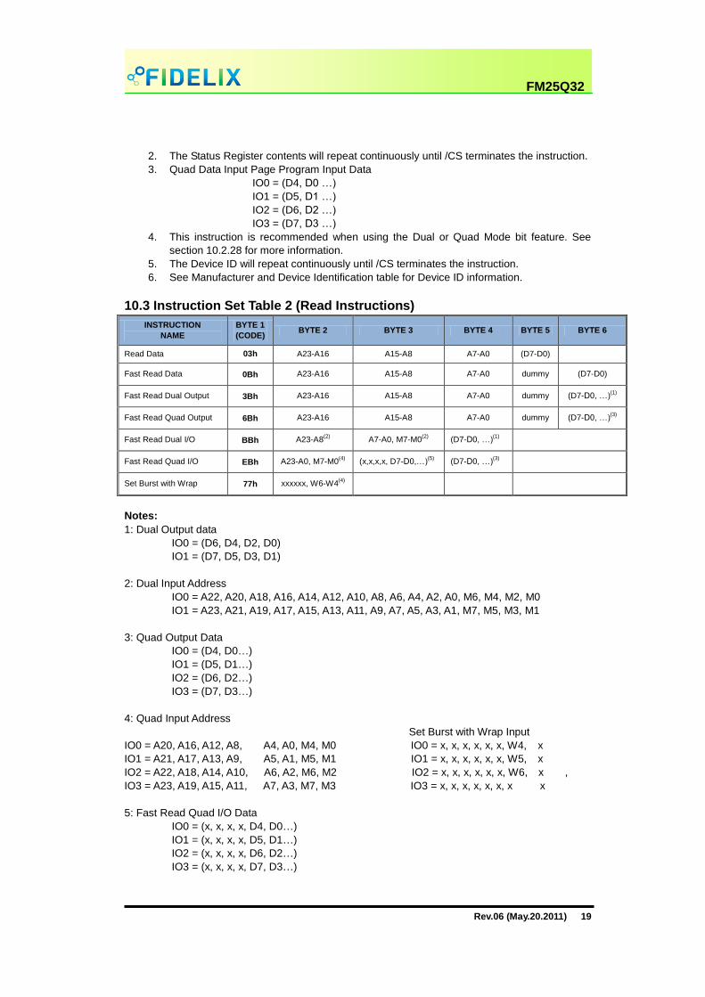
10.3 Instruction Set Table 2 (Read Instructions)
INSTRUCTION
NAME
BYTE 1
(CODE) BYTE 2 BYTE 3 BYTE 4 BYTE 5 BYTE 6
Read Data 03h A23-A16 A15-A8 A7-A0 (D7-D0)
Fast Read Data 0Bh A23-A16 A15-A8 A7-A0 dummy (D7-D0)
Fast Read Dual Output 3Bh A23-A16 A15-A8 A7-A0 dummy (D7-D0, …)(1)
Fast Read Quad Output 6Bh A23-A16 A15-A8 A7-A0 dummy (D7-D0, …)(3)
Fast Read Dual I/O BBh A23-A8(2)
A7-A0, M7-M0(2)
(D7-D0, …)(1)
Fast Read Quad I/O EBh A23-A0, M7-M0(4)
(x,x,x,x, D7-D0,…)(5)
(D7-D0, …)(3)
Set Burst with Wrap 77h xxxxxx, W6-W4(4)
Notes:
1: Dual Output data
IO0 = (D6, D4, D2, D0)
IO1 = (D7, D5, D3, D1)
2: Dual Input Address
IO0 = A22, A20, A18, A16, A14, A12, A10, A8, A6, A4, A2, A0, M6, M4, M2, M0
IO1 = A23, A21, A19, A17, A15, A13, A11, A9, A7, A5, A3, A1, M7, M5, M3, M1
3: Quad Output Data
IO0 = (D4, D0…)
IO1 = (D5, D1…)
IO2 = (D6, D2…)
IO3 = (D7, D3…)
4: Quad Input Address
Set Burst with Wrap Input
IO0 = A20, A16, A12, A8, A4, A0, M4, M0 IO0 = x, x, x, x, x, x, W4, x
IO1 = A21, A17, A13, A9, A5, A1, M5, M1 IO1 = x, x, x, x, x, x, W5, x
IO2 = A22, A18, A14, A10, A6, A2, M6, M2 IO2 = x, x, x, x, x, x, W6, x ,
IO3 = A23, A19, A15, A11, A7, A3, M7, M3 IO3 = x, x, x, x, x, x, x x
5: Fast Read Quad I/O Data
IO0 = (x, x, x, x, D4, D0…)
IO1 = (x, x, x, x, D5, D1…)
IO2 = (x, x, x, x, D6, D2…)
IO3 = (x, x, x, x, D7, D3…)

Rev.06 (May.20.2011) 20
FM25Q32
10.4 Write Enable (06h) Write Enable instruction is for setting the Write Enable Latch (WEL) bit in the Status Register. The
WEL bit must be set prior to every Program, Erase and Write Status Register instruction. To enter
the Write Enable instruction, /CS goes low prior to the instruction “06h” into Data Input (DI) pin on
the rising edge of CLK, and then driving /CS high.
Mode 0
Mode 3
Instruction
DI
DO
CLK
/CS
6543 70 1 2
High - Z
06h
Figure 5. Write Enable Instruction Sequence Diagram
10.5 Write Enable for Volatile Status Register (50h) This gives more flexibility to change the system configuration and memory protection schemes
quickly without waiting for the typical non-volatile bit write cycles or affecting the endurance of the
Status Register non-volatile bits. To write the volatile values into the Status Register bits, the Write
Enable for Volatile Status Register (50h) instruction must be issued prior to a Write Status Register
(01h) instruction. Write Enable for Volatile Status Register instruction (Figure 6) will not set the
Write Enable Latch (WEL) bit, it is only valid for the Write Status Register instruction to change the
volatile Status Register bit values
Mode 0
Mode 3
Instruction
DI
DO
CLK
/CS
6543 70 1 2
High - Z
50h
Figure 6. Write Enable for Volatile Status Register Instruction Sequence Diagram
Rev.06 (May.20.2011) 21
FM25Q32
10.6 Write Disable (04h) The Write Disable instruction is to reset the Write Enable Latch (WEL) bit in the Status Register.
The Write Disable instruction is entered by driving /CS low, sending the instruction code “04h” into
the DI pin and then driving /CS high. WEL bit is automatically reset write-disable status of “0” after
Power-up and upon completion of the every Program, Erase and Write Status Register instructions.
.
Mode 0
Mode 3
Instruction
DI
DO
CLK
/CS
6543 70 1 2
High - Z
04h
Figure 7. Write Disable Instruction Sequence Diagram
10.7 Read Status Register-1 (05h) and Read Status Register-2 (35h) The Read Status Register instructions are to read the Status Register. The Read Status Register
can be read at any time (every Program, Erase, Write Status Register and Write Security Register
cycle is in progress). It is recommended to check the BUSY bit before sending a new instruction
when a Program, Erase, Write Status Register or Write Status Register operation is in progress.
The instruction is entered by driving /CS low and sending the instruction code “05h” for Status
Register-1 or “35h” for Status Register-2 into the DI pin on the rising edge of CLK. The status
register bits are then shifted out on the DO pin at the falling edge of CLK with most significant bit
(MSB) first as shown in (figure 7). The Status Register bits are shown in figure 4a and 4b include
the BUSY, WEL, BP2-BP0, TB, SEC, SRP0, SRP1 and QE bits (see description of the Status
Register earlier in this datasheet).
The Status Register can be read continuously, as shown in (Figure 7). The instruction is completed
by driving /CS high.
Mode 0
Mode 3
05h or 35hDI
DO
CLK
/CS
6543 70 1 2
High - Z
131211108 9 14 20191817 2115 16 22 23
Instruction
7 6 5 4 3 2 1 0 7 6 5 4 3 2 1 0
Status Register 1 or 2 Out
MSB MSB
Status Register 1 or 2 Out
Figure 8. Read Status Register Instruction Sequence Diagram

Rev.06 (May.20.2011) 22
FM25Q32
10.8 Write Status Register (01h) The Write Status Register instruction is to write the Status Register. A Write Enable instruction must
previously have been issued prior to setting Write Status Register Instruction (Status Register bit
WEL must equal 1). Once write is enabled, the instruction is entered by driving /CS low, sending
the instruction code “01h”, and then writing the status register data byte or word as illustrated in
figure 9. The Status Register bits are shown in figure 4 and described earlier in this datasheet.
Only non-volatile Status Register bits SRP0, SEC, TB, BP2, BP1, BP0 (bits 7, 5, 4, 3, 2 of Status
Register-1) and QE, SRP1 (bits 9 and 8 of Status Register-2) can be written to. All other Status
Register bit locations are read-only and will not be affected by the Write Status Register instruction.
The /CS pin must be driven high after the eighth or sixteenth bit of data that is clocked in. If this is
not done the Write Status Register instruction will not be executed. If /CS is driven high after the
eighth clock, the QE and SRP1 bits will be cleared to 0. After /CS is driven high, the self-timed
Write Status Register cycle will commence for a time duration of tw (See AC Characteristics). While
the Write Status Register cycle is in progress, the Read Status Register instruction may still be
accessed to check the status of the BUSY bit. The BUSY bit is a 1 during the Write Status Register
cycle and a 0 when the cycle is finished and ready to accept other instructions again. After the
Write Status Register cycle has finished, The Write Enable Latch (WEL) bit in Status Register will
be cleared to 0.
The Write Status Register instruction can change the value of Block Protect bits (SEC, TB, BP2,
BP1 and BP0) to define the protected area of memory from erase and program instructions.
Protected areas become read-only (see Status Register Memory Protection table and description).
The Write Status Register instruction also allows the Status Register Protect bits (SRP0, SRP1) to
be set. Those bits are used in conjunction with the Write protect (/WP) pin, Lock out or OTP
features to disable writes to the status register. Please refer to 9 for detailed descriptions Status
Register protection methods. Factory default all Status Register bits are 0.
Mode 0
Mode 3
01hDI
DO
CLK
/CS
6543 70 1 2
High - Z
131211108 9 14 20191817 2115 16 22 23
Instruction
7 6 5 4 3 2 1 0 15 14 13 12 11 10 9 8
Status Register 1 In
MSB MSB
Status Register 2 In
Figure 9. Write Status Register Instruction Sequence Diagram

Rev.06 (May.20.2011) 23
FM25Q32
10.9 Read Data (03h) The Read Data instruction is to read data out from the device. The instruction is initiated by driving
the /CS pin low and then sending the instruction code “03h” with following a 24-bit address (A23-
A0) into the DI pin. The code and address bits are latched on the rising edge of the CLK pin. After
the address is received, the data byte of the addressed memory location will be shifted out on the
DO pin at the falling edge of CLK with most significant bit (MSB) first. The address is automatically
incremented to the next higher address after byte of data is shifted out allowing for a continuous
stream of data. This means that the entire memory can be accessed with a single instruction as
long as the clock continues. The instruction is completed by driving /CS high. The Read Data
instruction sequence is shown in (figure 10). If a Read Data instruction is issued while an Erase,
Program or Write Status Register cycle is in process (BUSY=1) the instruction is ignored and will
not have any effects on the current cycle. The Read Data instruction allows clock rates from D.C to
a maximum of fR (see AC Electrical Characteristics).
Mode 0
Mode 3
03hDI
DO
CLK
/CS
6543 70 1 2
High - Z
2928108 9 30 36353433 3731 32 38 39
Instruction
23 22 21 3 2 1 0
7 6 5 4 3 2 1 0
MSB
MSB
Data Out
24 Bit Address
7
Figure 10. Read Data Register Instruction Sequence Diagram
10.10 Fast Read (0Bh) The Fast Read instruction is high speed reading mode. The address is latched on the rising edge
of the CLK. After the 24-bit address, this is accomplished by adding eight “dummy” clocks as
shown in (figure 11). The dummy clocks means the internal circuits require time to set up the initial
address. During the dummy clocks, the data value on the DO pin is a “don’t care”. Data of each bit
shifts out on the falling edge of CLK.
Mode 0
Mode 3
0BhDI
DO
CLK
/CS
6543 70 1 2
High - Z
2928108 9 30 31
Instruction
23 22 21 3 2 1 0
MSB
24 Bit Address
DI
DO
CLK
/CS
38373635 3932 33 34
High - Z
4544434240 41 46 52515049 5347 48 54 55
Dummy Byte
7 6 5 4 3 2 1 0 7 6 5 4 3 2 1 0
MSB MSB
Data Out 1 Data Out 2
7 6 5 4 3 2 1 0
7
Figure 11. Fast Read Register Instruction Sequence Diagram

Rev.06 (May.20.2011) 24
FM25Q32
10.11 Fast Read Dual Output (3Bh) The Fast Read Dual Output instruction enable double throughput of Serial Flash in read mode.
This instruction is similar to the standard Fast Read (0Bh) instruction except that data is output on
two pins: IO0 and IO1, instead of just IO0. This allows data to be transferred from the FM25Q32 at
twice the rate of standard SPI devices. The Fast Read Dual Output instruction is ideal for quickly
downloading code from Flash to RAM upon power-up or for application that cache code-segments
to RAM for execution.
The Fast Read Dual Output instruction can operate at the highest possible frequency of FR (see AC
Electrical Characteristics). After the 24-bit address, this is accomplished by adding eight “dummy”
clocks as shown in (figure 12). The dummy clocks allow the internal circuits additional time for
setting up the initial address. During the dummy clocks, the data value on the DO pin is a “don’t
care”. However, the IO0 pin should be high-impedance prior to the falling edge of the first data out
clock.
Mode 0
Mode 3
3BhDI
DO
CLK
/CS
6543 70 1 2
High - Z
2928108 9 30 31
Instruction
23 22 21 3 2 1 0
MSB
24 Bit Address
DI
DO
CLK
/CS
38373635 3932 33 34
High - Z
4544434240 41 46 52515049 5347 48 54 55
Dummy Byte
Data Out 1
7 6 5 4 3 2 1 0
7 5 3 1 7 5 3 1 7 5 3 1 7 5 3 1
MSB MSB
7
6 4 2 0 6 4 2 0 6 4 2 0 6 4 2 0
MSB MSB
6
DI Switches from Input to Output
Data Out 2 Data Out 3 Data Out 4
Figure 12. Fast Read Dual Output Instruction Sequence Diagram

Rev.06 (May.20.2011) 25
FM25Q32
10.12 Fast Read Quad Output (6Bh) The Fast Read Dual Output instruction enable quad throughput of Serial Flash in read mode. The
Fast Read Quad Output instruction is similar to the Fast Read Dual Output (3Bh) instruction except
that data is output on four pins: IO0, IO1, IO2, and IO3. A Quad enable of Status Register-2 must be
executed before the device will accept the Fast Read Quad Output instruction (Status Register bit
QE must equal 1). The Fast Read Quad Output instruction allows data to be transferred from the
FM25Q32 at four times the rate of standard SPI devices.
The Fast Read Dual Output instruction can operate at the highest possible frequency of FR (see AC
Electrical Characteristics). This is accomplished by adding eight “dummy” clocks after the 24-bit
address as shown in (figure 13). The dummy clocks allow the internal circuits additional time for
setting up the initial address. During the dummy clocks, the data value on the DO pin is a “don’t
care”. However, the IO0 pin should be high-impedance prior to the falling edge of the first data out
clock.
Mode 0
Mode 3
6Bh
CLK
/CS
6543 70 1 2
High - Z
2928108 9 30 31
Instruction
23 22 21 3 2 1 0
MSB
24 Bit Address
CLK
/CS
36353433 3732 4342414038 39 44 45
46 47
IO0
IO1
IO2
IO3
Dummy
Data
Out 1
4 0 4
5 1 5
6 2 6
7 3 7
0
1
2
3 7
6
5
4
Data
Out 4
4 0 4
5 1 5
6 2 6
7 3 7
0
1
2
3
Data
Out 2
Data
Out 3
IO0 Switches from
Input to Output
IO0
IO1
IO2
IO3
High - Z
High - Z
Figure 13. Fast Read Quad Output Instruction Sequence Diagram

Rev.06 (May.20.2011) 26
FM25Q32
10.13 Fast Read Dual I/O (BBh) The Fast Read Dual I/O instruction reduce cycle overhead through double access using two IO
pins, IO0 and IO1.
“Continuous read mode”
The Fast Read Dual I/O instruction can further reduce instruction overhead through setting the
Mode bits (M7-0) after the input Address bits (A23-0), as shown in (figure 14a). The upper nibble of
the Mode (M7-4) controls the length of the next Fast Read Dual I/O instruction through the
inclusion or exclusion of the first byte instruction code. The lower nibble bits of the Mode (M3-0)
are don’t care (“X”), However, the IO pins should be high-impedance prior to the falling edge of the
first data out clock.
If the Mode bits (M7-0) equal “Ax” hex, then the next Fast Dual I/O instruction (after /CS is raised
and then lowered) does not require the BBh instruction code, as shown in (figure 14b). This
reduces the instruction sequence by eight clocks and allows the address to be immediately
entered after /CS is asserted low. If Mode bits (M7-0) are any value other “Ax” hex, the next
instruction (after /CS is raised and then lowered) requires the first byte instruction code, thus
returning to normal operation. A Mode Bit Reset instruction can be used to reset Mode Bits (M7-0)
before issuing normal instructions.
Mode 0
Mode 3
BBhDI
DO
CLK
/CS
6543 70 1 2
High - Z
Instruction
DI
DO
CLK
/CS
DI Switches from Input to Output
98 10 16151413 1711 12 18 19
23 21 19 17 15 13 11 9 7 5 3 1
22 20 18 16 14 12 10 8 6 4 2 0
A23 - 16 A15 - 8 A7 - 0
21 22 2320
24 Bit Address
M7 - 0
2928272624 25 30 36353433 3731 32 38 39
Data Out 1
7 5 3 1 7 5 3 1 7 5 3 1 7 5 3 1
MSB MSB
7
6 4 2 0 6 4 2 0 6 4 2 0 6 4 2 0
MSB MSB
6
Data Out 2 Data Out 3 Data Out 4
6 4
7 5High - Z
High - Z
Figure 14a. Fast Read Dual Input/Output Instruction Sequence Diagram (M7-0 = 0xh or NOT Axh)

Rev.06 (May.20.2011) 27
FM25Q32
Mode 0
Mode 3
DI
DO
CLK
/CS
6543 70 1 2
DI
DO
CLK
/CS
DI Switches from Input to Output
98 10 15141311 12
2120191816 17 22 28272625 2923 24 30 31
Data Out 1
7 5 3 1 7 5 3 1 7 5 3 1 7 5 3 1
MSB MSB
7
6 4 2 0 6 4 2 0 6 4 2 0 6 4 2 0
MSB MSB
6
Data Out 2 Data Out 3 Data Out 4
23 21 19 17 15 13 11 9 7 5 3 1
22 20 18 16 14 12 10 8 6 4 2 0
A23 - 16 A15 - 8 A7 - 0
24 Bit Address
M7 - 0
6 4
7 5High - Z
High - Z
Figure 14b. Fast Read Dual Input/Output Instruction Sequence Diagram (M7-0 = Axh)
Rev.06 (May.20.2011) 28
FM25Q32
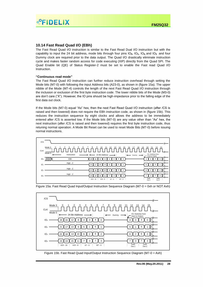
10.14 Fast Read Quad I/O (EBh) The Fast Read Quad I/O instruction is similar to the Fast Read Dual I/O instruction but with the
capability to input the 24 bit address, mode bits through four pins IO0, IO1, IO2, and IO3 and four
Dummy clock are required prior to the data output. The Quad I/O drastically eliminate instruction
cycle and makes faster random access for code executing (XIP) directly from the Quad SPI. The
Quad Enable bit (QE) of Status Register-2 must be set to enable the Fast read Quad I/O
Instruction.
“Continuous read mode”
The Fast Read Quad I/O instruction can further reduce instruction overhead through setting the
Mode bits (M7-0) with following the input Address bits (A23-0), as shown in (figure 15a). The upper
nibble of the Mode (M7-4) controls the length of the next Fast Read Quad I/O instruction through
the inclusion or exclusion of the first byte instruction code. The lower nibble bits of the Mode (M3-0)
are don’t care (“X”). However, the IO pins should be high-impedance prior to the falling edge of the
first data out clock.
If the Mode bits (M7-0) equal “Ax” hex, then the next Fast Read Quad I/O instruction (after /CS is
raised and then lowered) does not require the EBh instruction code, as shown in (figure 15b). This
reduces the instruction sequence by eight clocks and allows the address to be immediately
entered after /CS is asserted low. If the Mode bits (M7-0) are any value other than “Ax” hex, the
next instruction (after /CS is raised and then lowered) requires the first byte instruction code, thus
retuning normal operation. A Mode Bit Reset can be used to reset Mode Bits (M7-0) before issuing
normal instructions.
Mode 0
Mode 3
EBh
CLK
/CS
6543 70 1 2
High - Z
1312108 9 14 15
Instruction 24 Bit Address Dummy
IO0
IO1
IO2
IO3
High - Z
High - Z
A23 - 16
4 0 4
5 1 5
6 2 6
7 3 7
M7 - 0
20 16 12
21 17 13
22 18 14
23 19 15
8
9
10
11
A15 - 8 A7 - 0
0
1
2
3
1716 18 23222119 20
4 0 4
5 1 5
6 2 6
7 3 7
0
1
2
3 7
6
5
4
Data
Out 2
Data
Out 1
IOS Switches from
Input to Output
11
Figure 15a. Fast Read Quad Input/Output Instruction Sequence Diagram (M7-0 = 0xh or NOT Axh)
Mode 0
Mode 3
CLK
/CS
6543 70 1 2 1312108 9 14 15
IO0
IO1
IO2
IO3
11
24 Bit Address Dummy
A23 - 16
4 0 4
5 1 5
6 2 6
7 3 7
M7 - 0
20 16 12
21 17 13
22 18 14
23 19 15
8
9
10
11
A15 - 8 A7 - 0
0
1
2
3
4 0 4
5 1 5
6 2 6
7 3 7
0
1
2
3 7
6
5
4
Data
Out 2
Data
Out 1
IOS Switches from
Input to Output
Figure 15b. Fast Read Quad Input/Output Instruction Sequence Diagram (M7-0 = Axh)

Rev.06 (May.20.2011) 29
FM25Q32
10.15 Page Program (02h) The Page Program instruction is for programming the memory to be “0”. A Write Enable instruction
must be issued before the device accept the Page Program Instruction (Status Register bit WEL=
1). After the Write Enable (WREN) instruction has been decoded, the device sets the Write Enable
Latch (WEL). The instruction is entered by driving the /CS pin low and then shifting the instruction
code “02h” with following a 24-bits address (A23-A0) and at least one data byte, into the DI pin.
The /CS pin must be driven low for the entire time of the instruction while data is being sent to the
device. (Please refer to figure 16).
If the entire 256 data bytes are going to be programmed, A7-A0 (the eight least significant address
bits) should be set to 0. If more than 256 bytes are sent the device, previously latched data are
discarded and the last 256 data bytes are guaranteed to be programmed correctly within the same
page. If less than 256 data bytes are sent t device, they are correctly programmed at the requested
addresses without having any effects on the other bytes of the same page.
The /CS pin must be driven high after the eighth bit of the last byte has been latched in, otherwise
the Page Program instruction is not executed. After /CS is driven high, the self-timed Page
Program instruction will commence for a duration of tPP (See AC Characteristics). While the Page
Program cycle is in progress, the Read Status Register instruction may still be accessed for
checking the status of the BUSY bit. The BUSY bit is a 1 during the Page Program cycle and
becomes a 0 when the cycle is finished and the device is ready to accept other instructions again.
After the Page Program cycle has finished and Write Enable Latch (WEL) bit in the Status Register
is cleared to 0. The Page Program instruction applied to a page which is protected by the Block
Protect (SEC, TB, BP2, BP1, and BP0) bits is not executed.
DI
CLK
/CS
32 33 34 35
7 6 5 4
37 38 3936
4544434240 41 46 52515049 5347 48 54 55
7 6 5 4 3 2 1 0 7 6 5 4 3 2 1 0
3 2
Mode 0
Mode 3
02hDI
CLK
/CS
6543 70 1 2 2928108 9 30 31
Instruction
23 22 21 3 2 1 0
MSB
24 Bit Address
1 0
Data Byte 1
MSB
20
78
20
77
20
76
20
75
20
79
20
72
20
73
20
74
Data Byte 256
7 6 5 4 3 2 1 0
Data Byte 3Data Byte 2
MSB MSB MSB
Figure 16. Page Program Instruction Sequence Diagram

Rev.06 (May.20.2011) 30
FM25Q32
10.16 Quad Data Input Page Program (32h) The Quad Data Input Page Program instruction is to program the memory as being “0” at
previously erased (FFh) memory areas. The Quad Data Input Page Program takes four pins: IO0,
IO1, IO2 and IO3 as and data input, which can improve programmer performance and the
effectiveness of application of lower clock less than 5MHz. System using faster clock speed will not
get more benefit for the Quad Data Input Page Program as the required internal page program
time is far more than the time data clock-in.
To use Quad Data Input Page Program the Quad Enable in Status Register-2 must be set (QE=1),
A Write Enable instruction must be executed before the device will accept the Quad Data Input
Page Program instruction (Status Register-1, WEL=1). The instruction is initiated by driving the /CS
pin low and then shifting the instruction code “32h” with following a 24-bit address (A23-A0) and at
least one data, into the IO pins. The /CS pin must be held low for the entire length of the instruction
while data is being sent to the device. All other functions of Quad Data Input Page Program are
perfectly same as standard Page Program. (Please refer to figure 17).
Mode 0
Mode 3
32h
CLK
/CS
6543 70 1 2
High - Z
2928108 9 30 31
Instruction
23 22 21 3 2 1 0
MSB
24 Bit Address
43424140 4439 53
9
53
8
53
7
53
6
45 54
0
54
1
54
2
54
3
Data
Byte 253
4 0 4
5 1 5
6 2 6
7 3 7
0
1
2
3
Data
Byte 256
4 0 4
5 1 5
6 2 6
7 3 7
0
1
2
3
Data
Byte 254
Data
Byte 255
IO0
IO1
IO2
IO3
High - Z
High - Z
Data
Byte 1
4 0 4
5 1 5
6 2 6
7 3 7
0
1
2
3
Data
Byte 2
3332 34 35
CLK
/CS
IO0
IO1
IO2
IO3
Data
Byte 4
4 0 4
5 1 5
6 2 6
7 3 7
0
1
2
3
Data
Byte 7
4 0 4
5 1 5
6 2 6
7 3 7
0
1
2
3
Data
Byte 5
Data
Byte 6
383736
4 0
5 1
6 2
7 3
Data
Byte 3
Figure 17. Quad Data Input Page Program Instruction Sequence Diagram

Rev.06 (May.20.2011) 31
FM25Q32
10.17 Quad Page Program (38h) The Quad Data Input Page Program instruction is to program the memory as being “0” at
previously erased (FFh) memory areas. The Quad Data Input Page Program takes four pins: IO0,
IO1, IO2 and IO3 as address and data input, which can improve programmer performance and the
effectiveness of application of lower clock less than 5MHz. System using faster clock speed will not
get more benefit for the Quad Data Input Page Program as the required internal page program
time is far more than the time data clock-in.
To use Quad Data Input Page Program the Quad Enable in Status Register-2 must be set (QE=1),
A Write Enable instruction must be executed before the device will accept the Quad Data Input
Page Program instruction (Status Register-1, WEL=1). The instruction is initiated by driving the /CS
pin low then shifting the instruction code “38h” with following a 24-bit address (A23-A0) and at least
one data, into the IO pins. The /CS pin must be held low for the entire length of the instruction
while data is being sent to the device. All other functions of Quad Page Program are perfectly
same as standard Page Program. (Please refer to figure 18).
Mode 0
Mode 3
38h
CLK
/CS
6543 70 1 2
High - Z
1312108 9 14 15
Instruction
MSB
24 Bit Address
27262524 2823 52
1
52
0
51
9
51
8
29 52
2
52
3
52
4
52
5
Data
Byte 253
4 0 4
5 1 5
6 2 6
7 3 7
0
1
2
3
Data
Byte 256
4 0 4
5 1 5
6 2 6
7 3 7
0
1
2
3
Data
Byte 254
Data
Byte 255
IO0
IO1
IO2
IO3
High - Z
High - Z
Data
Byte 2
4 0 4
5 1 5
6 2 6
7 3 7
0
1
2
3
Data
Byte 3
1716 18 19
CLK
/CS
IO0
IO1
IO2
IO3
Data
Byte 5
4 0 4
5 1 5
6 2 6
7 3 7
0
1
2
3
Data
Byte 8
4 0 4
5 1 5
6 2 6
7 3 7
0
1
2
3
Data
Byte 6
Data
Byte 7
222120
4 0
5 1
6 2
7 3
Data
Byte 4
4 0
5 1
6 2
7 3
12 8 4
13 9 5
14 10 6
15 11 7
0
1
2
3
Data
Byte 1
20 16
21 17
22 18
23 19
11
Figure 18. Quad Page Program Instruction Sequence Diagram

Rev.06 (May.20.2011) 32
FM25Q32
10.18 Sector Erase (20h) The Sector Erase instruction is to erase the data of the selected sector as being “1”. The
instruction is used for an 4K-byte sector. Prior to the Sector Erase Instruction, a Write Enable
instruction must be issued. (Status Register bit WEL must be equal to 1). The instruction is initiated
by driving the /CS pin low and shifting the instruction code “20h” followed a 24-bit sector address
(A23-A0). (Please refer to figure 19).
The /CS pin must be driven high after the eighth bit of the last byte has been latched in, oherwise
the Sector Erase instruction will not be executed. After /CS is driven high, the self-timed Sector
Erase instruction will commence for a time duration of tSE (See AC Characteristics). While the
Sector Erase cycle is in progress, the Read Status Register instruction may still be accessed for
checking the status of the BUSY bit. The BUSY bit is a 1 during the Sector Erase cycle and
becomes a 0 when the cycle is finished and the device is ready to accept other instructions again.
After the Sector Erase cycle has finished the Write Enable Latch (WEL) bit in Status Register is
cleared to 0. The Sector Erase instruction applied to addressed page which is protected by the
Block Protect (SEC, TB, BP2, BP1, and BP0) bits is not executed. (see Status Register Memory
protection table).
Mode 0
Mode 3
20hDI
DO
CLK
/CS
6543 70 1 2
High - Z
2928108 9 30 31
Instruction
23 22 21 3 2 1 0
MSB
24 Bit Address
Figure 19. Sector Erase Instruction Sequence Diagram

Rev.06 (May.20.2011) 33
FM25Q32
10.19 32KB Block Erase (52h) The Block Erase instruction is to erase the data of the selected block as being “1”. The instruction
is used for an 32K-byte Block erase operation. Prior to the Block Erase Instruction, a Write Enable
instruction must be issued. (Status Register bit WEL must equal 1). The instruction is initiated by
driving the /CS pin low and shifting the instruction code “52h” followed a 24-bit block address (A23-
A0). (Please refer to figure 20).
The /CS pin must be driven high after the eighth bit of the last byte has been latched in, otherwise
the Block Erase instruction will not be issued. After /CS is driven high, the self-timed Block Erase
instruction will commence for a time duration of tBE1 (See AC Characteristics). While the Block
Erase cycle is in progress, the Read Status Register instruction may still be accessed for checking
the status of the BUSY bit. The BUSY bit is a 1 during the Block Erase cycle and becomes a 0
when the cycle is finished and the device is ready to accept other instructions again.
After the Sector Erase cycle has finished the Write Enable Latch (WEL) bit in Status Register is
cleared to 0.The Block Erase instruction applied to addressed page which is protected by the Block
Protect (SEC, TB, BP2, BP1, and BP0) bits is not executed. (see Status Register Memory
Protection table).
Mode 0
Mode 3
52hDI
DO
CLK
/CS
6543 70 1 2
High - Z
2928108 9 30 31
Instruction
23 22 21 3 2 1 0
MSB
24 Bit Address
Figure 20. 32KB Block Erase Instruction Sequence Diagram
Rev.06 (May.20.2011) 34
FM25Q32
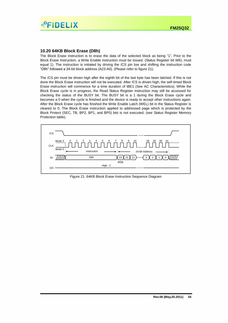
10.20 64KB Block Erase (D8h) The Block Erase instruction is to erase the data of the selected block as being “1”. Prior to the
Block Erase Instruction, a Write Enable instruction must be issued. (Status Register bit WEL must
equal 1). The instruction is initiated by driving the /CS pin low and shifting the instruction code
“D8h” followed a 24-bit block address (A23-A0). (Please refer to figure 21).
The /CS pin must be driven high after the eighth bit of the last byte has been latched. If this is not
done the Block Erase instruction will not be executed. After /CS is driven high, the self-timed Block
Erase instruction will commence for a time duration of tBE1 (See AC Characteristics). While the
Block Erase cycle is in progress, the Read Status Register instruction may still be accessed for
checking the status of the BUSY bit. The BUSY bit is a 1 during the Block Erase cycle and
becomes a 0 when the cycle is finished and the device is ready to accept other instructions again.
After the Block Erase cycle has finished the Write Enable Latch (WEL) bit in the Status Register is
cleared to 0. The Block Erase instruction applied to addressed page which is protected by the
Block Protect (SEC, TB, BP2, BP1, and BP0) bits is not executed. (see Status Register Memory
Protection table).
Mode 0
Mode 3
D8hDI
DO
CLK
/CS
6543 70 1 2
High - Z
2928108 9 30 31
Instruction
23 22 21 3 2 1 0
MSB
24 Bit Address
Figure 21. 64KB Block Erase Instruction Sequence Diagram

Rev.06 (May.20.2011) 35
FM25Q32
10.21 Chip Erase (C7h / 60h) The Chip-Erase instruction clears all bits in the device to be FFh (all 1s). A Chip-Erase instruction
will be ignored if any of the memory area is protected. Prior to any Write operation, the Write-
Enable (WREN) instruction must be executed. The instruction is initiated by driving the /CS pin low
and shifting the instruction code “C7h” or “60h”. (Please refer to figure 22).
The /CS pin must be driven high after the eighth bit has been latched. If this is not done the Chip
Erase instruction will not be executed. After /CS is driven high, the self-timed Chip Erase
instruction will commence for a duration of tCE (See AC Characteristics). While the Chip Erase
cycle is in progress, the Read Status Register instruction may still be accessed to check the status
of the BUSY bit. The BUSY bit is a 1 during the Chip Erase cycle and becomes a 0 when the cycle
is finished and the device is ready to accept other instructions again. After the Chip Erase cycle
has finished the Write Enable Latch (WEL) bit in the Status Register is cleared to 0. The Chip
Erase instruction applied to a page which is protected by the Block Protect (SEC, TB, BP2, BP1,
and BP0) bits is not executed. (see Status Register Memory Protection table).
Mode 0
Mode 3
Instruction
DI
DO
CLK
/CS
6543 70 1 2
High - Z
C7h or 60h
Figure 22. Chip Erase Instruction Sequence Diagram
Rev.06 (May.20.2011) 36
FM25Q32
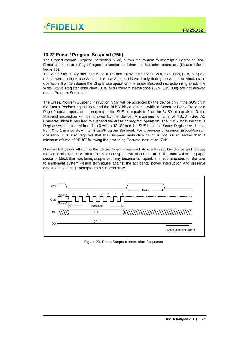
10.22 Erase / Program Suspend (75h) The Erase/Program Suspend instruction “75h”, allows the system to interrupt a Sector or Block
Erase operation or a Page Program operation and then conduct other operation. (Please refer to
figure 23).
The Write Status Register instruction (01h) and Erase instructions (20h, 52h, D8h, C7h, 60h) are
not allowed during Erase Suspend. Erase Suspend is valid only during the Sector or Block erase
operation. If written during the Chip Erase operation, the Erase Suspend instruction is ignored. The
Write Status Register instruction (01h) and Program instructions (02h, 32h, 38h) are not allowed
during Program Suspend.
The Erase/Program Suspend instruction “75h” will be accepted by the device only if the SUS bit in
the Status Register equals to 0 and the BUSY bit equals to 1 while a Sector or Block Erase or a
Page Program operation is on-going. If the SUS bit equals to 1 or the BUSY bit equals to 0, the
Suspend instruction will be ignored by the device. A maximum of time of “tSUS” (See AC
Characteristics) is required to suspend the erase or program operation. The BUSY bit in the Status
Register will be cleared from 1 to 0 within “tSUS” and the SUS bit in the Status Register will be set
from 0 to 1 immediately after Erase/Program Suspend. For a previously resumed Erase/Program
operation, it is also required that the Suspend instruction “75h” is not issued earlier than a
minimum of time of “tSUS” following the preceding Resume instruction “7Ah”.
Unexpected power off during the Erase/Program suspend state will reset the device and release
the suspend state. SUS bit in the Status Register will also reset to 0. The data within the page,
sector or block that was being suspended may become corrupted. It is recommended for the user
to implement system design techniques against the accidental power interruption and preserve
data integrity during erase/program suspend state.
Mode 0
Mode 3
75hDI
DO
CLK
/CS
6543 70 1 2
High - Z
Instruction
tSUS
Acceptable Instructions
Figure 23. Erase Suspend instruction Sequence

Rev.06 (May.20.2011) 37
FM25Q32
10.23 Erase / Program Resume (7Ah) The Erase/Program Resume instruction “7Ah” is to re-work the Sector or Block Erase operation or
the Page Program operation upon an Erase/Program Suspend. The Resume instruction “7Ah” will
be accepted by the device only if the SUS bit in the Status Register equals to 1 and the BUSY bit
equals to 0. After issued, the SUS bit will be cleared from 1 to 0 immediately, the BUSY bit will be
set from 0 to 1 within 200ns and the Sector or Block will complete the erase operation or the page
will complete the program operation. If the SUS bit equals to 0 or the BUSY bit equals to 1, the
Resume instruction “7Ah” will be ignored by the device.
Resume instruction can not be accepted if the previous Erase/Program Suspend operation was
interrupted by unexpected power off. It is also required that a subsequent Erase/Program Suspend
instruction not to be issued within a minimum of time of “tSUS” following a previous Resume
instruction. (Please refer to figure 24).
Mode 0
Mode 3
7AhDI
CLK
/CS
6543 70 1 2
Instruction
Resume previously Suspended
Program or Erase
Figure 24. Erase / Program Resume instruction Sequence
Rev.06 (May.20.2011) 38
FM25Q32
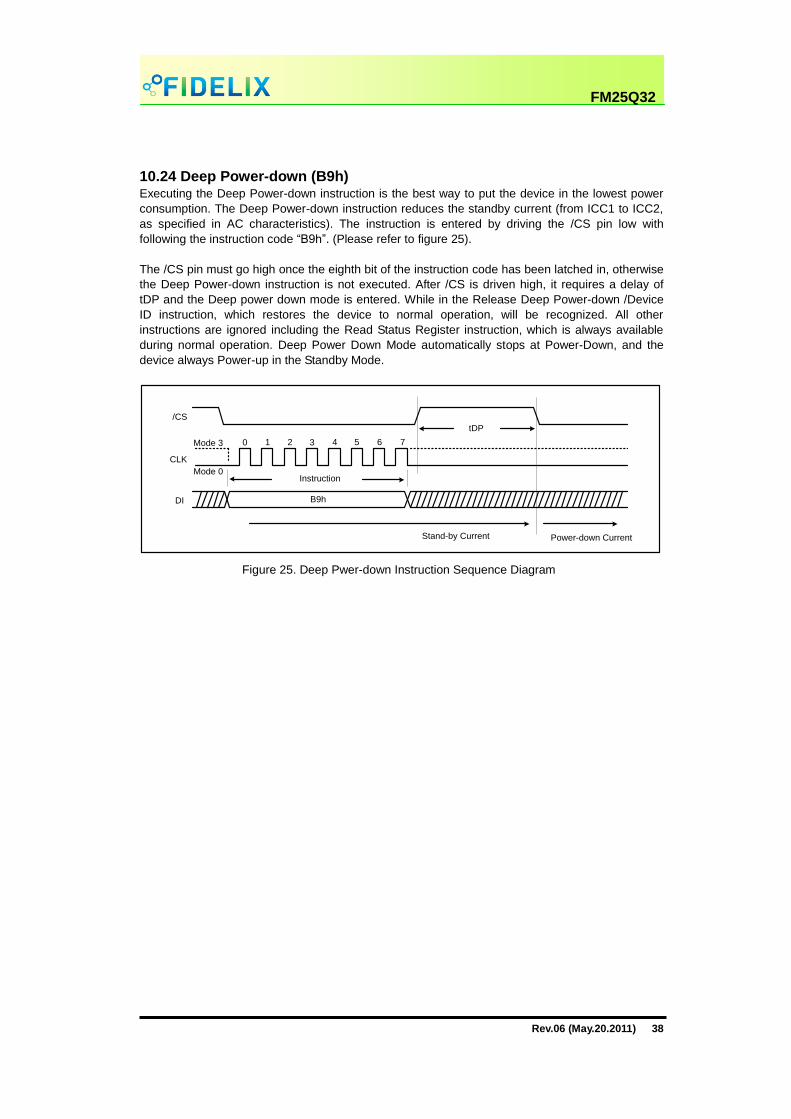
10.24 Deep Power-down (B9h) Executing the Deep Power-down instruction is the best way to put the device in the lowest power
consumption. The Deep Power-down instruction reduces the standby current (from ICC1 to ICC2,
as specified in AC characteristics). The instruction is entered by driving the /CS pin low with
following the instruction code “B9h”. (Please refer to figure 25).
The /CS pin must go high once the eighth bit of the instruction code has been latched in, otherwise
the Deep Power-down instruction is not executed. After /CS is driven high, it requires a delay of
tDP and the Deep power down mode is entered. While in the Release Deep Power-down /Device
ID instruction, which restores the device to normal operation, will be recognized. All other
instructions are ignored including the Read Status Register instruction, which is always available
during normal operation. Deep Power Down Mode automatically stops at Power-Down, and the
device always Power-up in the Standby Mode.
Mode 0
Mode 3
B9hDI
CLK
/CS
6543 70 1 2
Instruction
tDP
Power-down CurrentStand-by Current
Figure 25. Deep Pwer-down Instruction Sequence Diagram

Rev.06 (May.20.2011) 39
FM25Q32
10.25 Release Deep Power-down / Device ID (ABh) The Release from Deep Power-down / Device ID instruction is a multi-purpose instruction. It can
be used to release the device from the Deep Power-down state or obtain the device electronic
identification (ID) number.
To release the device from the Deep Power-down state, the instruction is issued by driving the /CS
pin low, sending the instruction code “ABh” and driving /CS high as shown in figure 26a. Release
from Deep Power-down require the time duration of tRES1 (See AC Characteristics) for re-work a
normal operation and accepting other instructions. The /CS pin must keep high during the tRES1
time duration.
When used only to obtain the Device ID while not in the Deep Power-down state, instruction is
initiated by driving the /CS pin low and sending the instruction code “ABh” with following 3-dummy
bytes. The Device ID bits are then shifted on the falling edge of CLK with most significant bit (MSB)
first as shown in figure 26b. The Device ID value for the FM25Q32 is listed in Manufacturer and
Device Identification table. The Device ID can be read continuously. The instruction is completed
by driving /CS high.
When used to release the device from the Deep Power-down state and obtain the Device ID, the
instruction is the same as previously described, and shown in figure 26b, except that after /CS is
driven high it must keep high for a time duration of tRES2 (See AC Characteristics). After this time
duration the device will resume normal operation and other instructions can be accepted. If the
Release from Deep Power-down /Device ID instruction is issued while an Erase, Program or Write
cycle is in process (when BUSY equals 1) the instruction is ignored and will not have any effects
on the current cycle.
Mode 0
Mode 3
ABhDI
CLK
/CS
6543 70 1 2
Instruction
tRES1
Power-down Current Stand-by Current
Figure 26a. Release Deep Power-down Instruction Sequence
Power-down Current Stand-by
Current
Mode 0
Mode 3
ABhDI
DO
CLK
/CS
6543 70 1 2
High - Z
2928108 9 30 36353433 3731 32 38
Instruction
7 6 5 4 3 2 1 0
MSB
Device ID (15h)
23 22 21 3 2 1 0
3 Dummy Bytes
MSB
39
tRES2
Figure 26b. Release Deep Power-down / Device ID Instruction Sequence Diagram
Rev.06 (May.20.2011) 40
FM25Q32
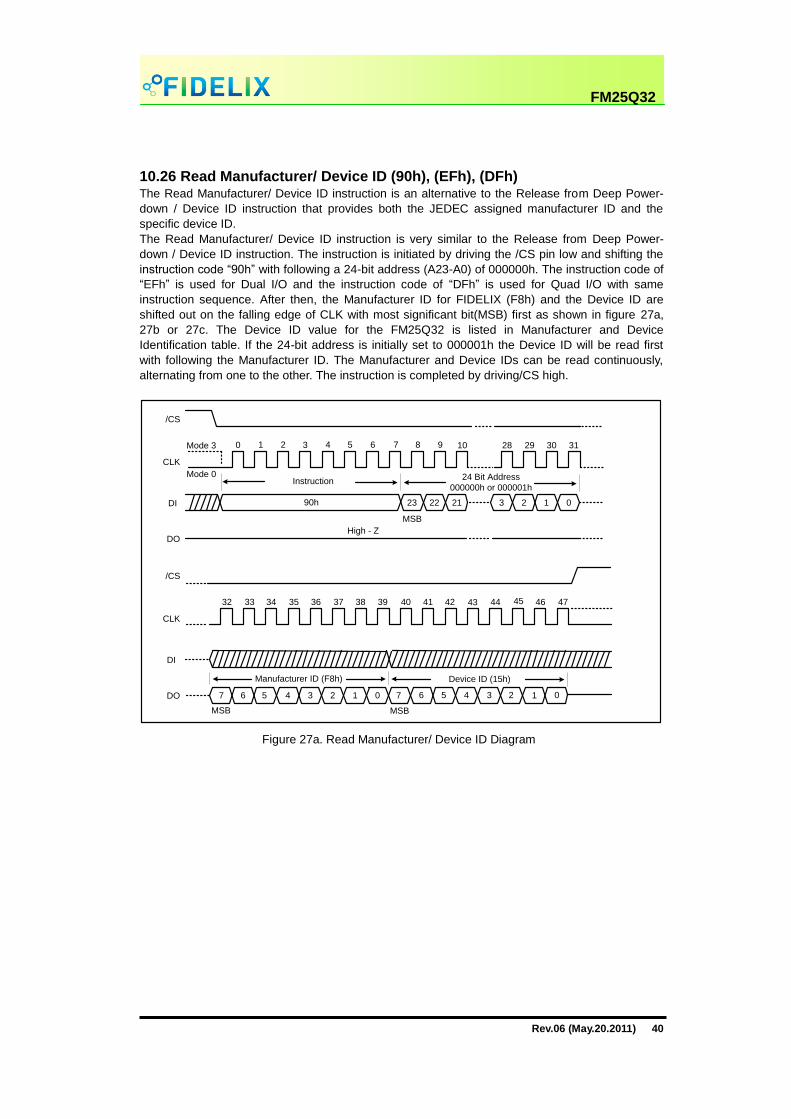
10.26 Read Manufacturer/ Device ID (90h), (EFh), (DFh) The Read Manufacturer/ Device ID instruction is an alternative to the Release from Deep Power-
down / Device ID instruction that provides both the JEDEC assigned manufacturer ID and the
specific device ID.
The Read Manufacturer/ Device ID instruction is very similar to the Release from Deep Power-
down / Device ID instruction. The instruction is initiated by driving the /CS pin low and shifting the
instruction code “90h” with following a 24-bit address (A23-A0) of 000000h. The instruction code of
“EFh” is used for Dual I/O and the instruction code of “DFh” is used for Quad I/O with same
instruction sequence. After then, the Manufacturer ID for FIDELIX (F8h) and the Device ID are
shifted out on the falling edge of CLK with most significant bit(MSB) first as shown in figure 27a,
27b or 27c. The Device ID value for the FM25Q32 is listed in Manufacturer and Device
Identification table. If the 24-bit address is initially set to 000001h the Device ID will be read first
with following the Manufacturer ID. The Manufacturer and Device IDs can be read continuously,
alternating from one to the other. The instruction is completed by driving/CS high.
Mode 0
Mode 3
90hDI
DO
CLK
/CS
6543 70 1 2
High - Z
2928108 9 30 31
Instruction
23 22 21 3 2 1 0
MSB
24 Bit Address
000000h or 000001h
DI
DO
CLK
/CS
3736353432 33 38 44434241 4539 40 46 47
7 6 5 4 3 2 1 0 7 6 5 4 3 2 1 0
MSB MSB
Manufacturer ID (F8h) Device ID (15h)
Figure 27a. Read Manufacturer/ Device ID Diagram

Rev.06 (May.20.2011) 41
FM25Q32
Mode 0
Mode 3
EFhDI
DO
CLK
/CS
6543 70 1 2
High - Z
Instruction
DI
DO
CLK
/CS
DI Switches from Input to Output
98 10 15141312
23 22 21 3 2 1 0
24 Bit Address
2928272624 25 30 36353433 3731 32 38 39
Manufacturer
ID (F8h)
7 5 3 1 7 5 3 1 7 5 3 1 7 5 3 1
MSB MSB
7
6 4 2 0 6 4 2 0 6 4 2 0 6 4 2 0
MSB MSB
6
Device ID
(15h)
Manufacturer
ID (F8h)
Device ID
(15h)
Figure 27b. Read Dual Manufacturer/ Device ID Diagram
Mode 0
Mode 3
DFh
CLK
/CS
6543 70 1 2
High - Z
Instruction
98 10 15141312
23 22 21 3 2 1 0
24 Bit Address
2726252423
CLK
/CS
IO0
IO1
IO2
IO3
Device
ID (15h)
4 0
5 1
6 2
7 3
4 0 4
5 1 5
6 2 6
7 3 7
0
1
2
3
Manufacturer
ID (F8h)
Device
ID (15h)
222120
4 0
5 1
6 2
7 3
Manufacturer
ID (F8h)
IOs Switches from
Input to Output
IO0
IO1
IO2
IO3
High - Z
High - Z
Figure 27c. Read Quad Manufacturer/ Device ID Diagram

Rev.06 (May.20.2011) 42
FM25Q32
10.27 JEDEC ID (9Fh) For compatibility reasons, the FM25Q32 provides several instructions to electronically determine
the identity of the device. The Read JEDEC ID instruction is congruous with the JEDEC standard
for SPI compatible serial flash memories that was adopted in 2003. The instruction is entered by
driving the /CS pin low with following the instruction code “9Fh”. JEDEC assigned Manufacturer ID
byte for FIDELIX (F8h) and two Device ID bytes, Memory Type(ID-15-ID8) and Capacity (ID7-ID0)
are then shifted out on the falling edge of CLK with most significant bit (MSB) first shown in figure
28. For memory type and capacity values refer to Manufacturer and Device Identification table. The
JEDEC ID can be read continuously. The instruction is terminated by driving/CS high.
Mode 0
Mode 3
9FhDI
DO
CLK
/CS
6543 70 1 2
High - Z
1312108 9 14 15
Instruction
DI
DO
CLK
/CS
2120191816 17 22 28272625 2923 24 30 31
Memory Type ID15 - 8 Capacity Type ID7 - 0
11
Manufacturer ID
F8h
32h 16h
Figure 28. Read JEDEC ID

Rev.06 (May.20.2011) 43
FM25Q32
10.28 Read Serial Flash Discovery Parameter (5Ah) The Read Serial Flash Discovery Parameter (SFDP) instruction allows reading the Serial
Flash Discovery Parameter area (SFDP). This SFDP area is composed of 2048 read-only bytes
containing operating characteristics and vendor specific information. The SFDP area is factory
programmed. If the SFDP area is blank, the device is shipped with all the SFDP bytes at FFh. If
only a portion of the SFDP area is written to, the portion not used is shipped with bytes in erased
state (FFh). The instruction sequence for the read SFDP has the same structure as that of a Fast
Read instruction. First, the device is selected by driving Chip Select (/CS) Low. Next, the 8-bit
instruction code (5Ah) and the 24-bit address are shifted in, with following 8 dummy clock cycles.
The bytes of SFDP content are shifted out on the Serial Data Output (DO) starting from the
specified address. Each bit is shifted out during the falling edge of Serial Clock (CLK). The
instruction sequence is shown here. The Read SFDP instruction is terminated by driving Chip
Select (/CS) High at any time during data output.
Mode 0
Mode 3
5AhDI
DO
CLK
/CS
6543 70 1 2
High - Z
2928108 9 30 31
Instruction
23 22 21 3 2 1 0
MSB
24 Bit Address
DI
DO
CLK
/CS
38373635 3932 33 34
High - Z
4544434240 41 46 52515049 5347 48 54 55
Dummy Byte
7 6 5 4 3 2 1 0 7 6 5 4 3 2 1 0
MSB MSB
Data Out 1 Data Out 2
7 6 5 4 3 2 1 0
7
Figure 29. Read SFDP Register Instruction Sequence Diagram

Rev.06 (May.20.2011) 44
FM25Q32
Read Serial Flash Discovery Parameter(SFDP)
BYTE
ADDRESS DATA DESCRIPTION COMMENT
00h 53h SFDP Signature
SFDP Signature
=50444653h
01h 46h SFDP Signature
02h 44h SFDP Signature
03h 50h SFDP Signature
04h 01h SFDP Minor Revisions SFDP revision 1.1
05h 01h SFDP Major Revisions
06h 00h Number of Parameter Header(NPH) 1 Parameter Header
07h FFh Reserved
08h F8h PID(0)(3)
: Manufacture JEDEC ID F8h = Fidelix
09h 00h PID(0) : Serial Flash Basics Minor Revisions Serial Flash Basics
Revision 1.0 0Ah 01h PID(0) : Serial Flash Basics Major Revisions
0Bh 04h PID(0) : Serial Flash Basics Length 4 Dwords (2)
0Ch 80h PID(0) : Address of Parameter ID(0) Table (A7-A0) PID(0) Table Address
= 000080h 0Dh 00h PID(0) : Address of Parameter ID(0) Table (A15-A8)
0Eh 00h PID(0) : Address of Parameter ID(0) Table (A23-A16)
0Fh FFh Reserved
10h F8h PID(1) : Manufacture JEDEC ID F8h = Fidelix
11h 00h PID(1) : Serial Flash Properties Minor Revisions Serial Flash Basics
Revision 1.0 12h 01h PID(1) : Serial Flash Properties Major Revisions
13h 00h PID(1) : Serial Flash Properties Length 00h = Unimplemented
14h 90h PID(1) : Address of Parameter ID(0) Table (A7-A0) PID(1) Table Address
= 000090h 15h 00h PID(1) : Address of Parameter ID(0) Table (A15-A8)
16h 00h PID(1) : Address of Parameter ID(0) Table (A23-A16)
17h FFh Reserved
... (1)
FFh Reserved
80h E5h Bit[7:5] = 111 Reserved
Bit[4:3] = 00 Non-volatile Status Register
Bit[2] = 1 Page Programmable
Bit[1:0] = 01 Support 4KB Erase

Rev.06 (May.20.2011) 45
FM25Q32
Read Serial Flash Discovery Parameter(SFDP) (cont’d)
BYTE
ADDRESS DATA DESCRIPTION COMMENT
81h 20h 4K-Byte Erase Opcode
82h F1h
Bit[7] = 1 Reserved
Bit[6] = 1 Supports Single Input Quad Output
Bit[5] = 1 Supports Quad Input Quad Output
Bit[4] = 1 Supports Dual Input Dual Output
Bit[3] = 0 Dual Transfer Rate not Supported
Bit[2:1] = 00 3-Byte/24-Bit Addressing
Bit[1] = 1 Supports Single Input Dual Output
83h FFh Reserved
84h FFh Flash Size in Bits
32 Mega Bits =
01FFFFFFh
85h FFh Flash Size in Bits
86h FFh Flash Size in Bits
87h 01h Flash Size in Bits
88h 44h Bit[7:5] = 010 8 Mode Bits are needed Fast Read
Quad I/O
Setting
Bit[4:0] = 00100 16 Dummy Bits are needed
89h EBh Quad Input Quad Output Fast Read Opcode
8Ah 08h Bit[7:5] = 000 No Mode Bits are needed Fast Read
Quad Output
Setting
Bit[4:0] = 01000 8 Dummy Bits are needed
8Bh 6Bh Single Input Quad Output Fast Read Opcode
8Ch 08h Bit[7:5] = 000 No Mode Bits are needed Fast Read
Dual Output
Setting
Bit[4:0] = 01000 8 Dummy Bits are needed
8Dh 3Bh Single Input Dual Output Fast Read Opcode
8Eh 80h Bit[7:5] = 100 8 Mode Bits are needed Fast Read
Dual I/O
Setting
Bit[4:0] = 00000 No Dummy Bits are needed
8Fh BBh Dual Input Dual Output Fast Read Opcode
...(1)
FFh Reserved
EFh FFh Reserved
F0h-FFh xxh Reserved
Notes:
1. Data stored in Byte Address 18h to 7Fh & 90h to FFh are Reserved, the value is FFh.
2. 1 Dword = 4 Bytes.
3. PID(x) = Parameter Identification Table(x)
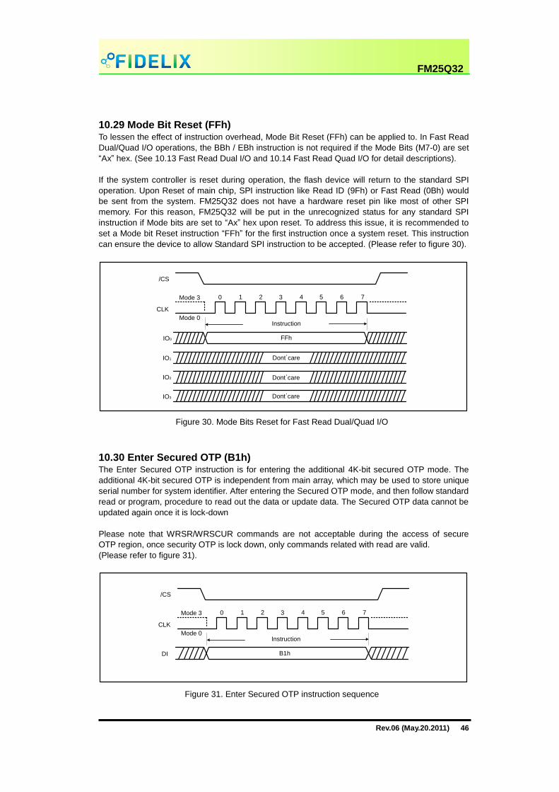
Rev.06 (May.20.2011) 46
FM25Q32
10.29 Mode Bit Reset (FFh) To lessen the effect of instruction overhead, Mode Bit Reset (FFh) can be applied to. In Fast Read
Dual/Quad I/O operations, the BBh / EBh instruction is not required if the Mode Bits (M7-0) are set
“Ax” hex. (See 10.13 Fast Read Dual I/O and 10.14 Fast Read Quad I/O for detail descriptions).
If the system controller is reset during operation, the flash device will return to the standard SPI
operation. Upon Reset of main chip, SPI instruction like Read ID (9Fh) or Fast Read (0Bh) would
be sent from the system. FM25Q32 does not have a hardware reset pin like most of other SPI
memory. For this reason, FM25Q32 will be put in the unrecognized status for any standard SPI
instruction if Mode bits are set to “Ax” hex upon reset. To address this issue, it is recommended to
set a Mode bit Reset instruction “FFh” for the first instruction once a system reset. This instruction
can ensure the device to allow Standard SPI instruction to be accepted. (Please refer to figure 30).
Mode 0
Mode 3
Instruction
CLK
/CS
6543 70 1 2
Dont’care
FFh
IO1
IO2
IO3
IO0
Dont’care
Dont’care
Figure 30. Mode Bits Reset for Fast Read Dual/Quad I/O
10.30 Enter Secured OTP (B1h) The Enter Secured OTP instruction is for entering the additional 4K-bit secured OTP mode. The
additional 4K-bit secured OTP is independent from main array, which may be used to store unique
serial number for system identifier. After entering the Secured OTP mode, and then follow standard
read or program, procedure to read out the data or update data. The Secured OTP data cannot be
updated again once it is lock-down
Please note that WRSR/WRSCUR commands are not acceptable during the access of secure
OTP region, once security OTP is lock down, only commands related with read are valid.
(Please refer to figure 31).
Mode 0
Mode 3
Instruction
DI
CLK
/CS
6543 70 1 2
B1h
Figure 31. Enter Secured OTP instruction sequence
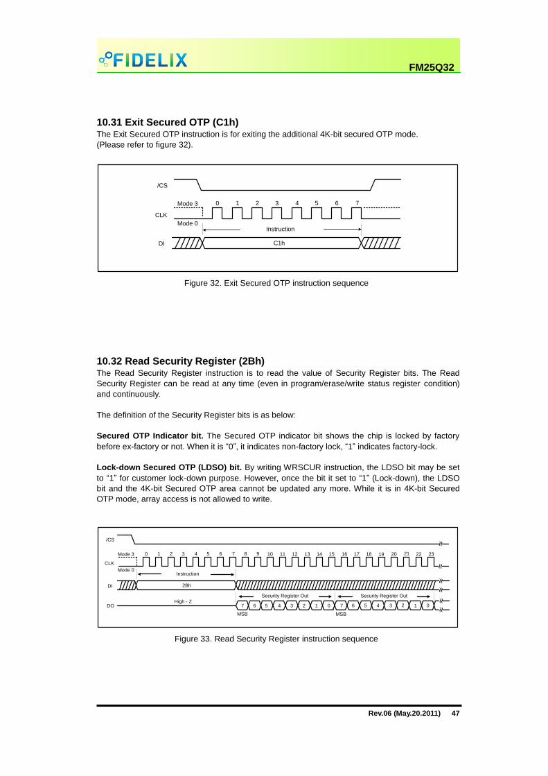
Rev.06 (May.20.2011) 47
FM25Q32
10.31 Exit Secured OTP (C1h) The Exit Secured OTP instruction is for exiting the additional 4K-bit secured OTP mode.
(Please refer to figure 32).
Mode 0
Mode 3
Instruction
DI
CLK
/CS
6543 70 1 2
C1h
Figure 32. Exit Secured OTP instruction sequence
10.32 Read Security Register (2Bh) The Read Security Register instruction is to read the value of Security Register bits. The Read
Security Register can be read at any time (even in program/erase/write status register condition)
and continuously.
The definition of the Security Register bits is as below:
Secured OTP Indicator bit. The Secured OTP indicator bit shows the chip is locked by factory
before ex-factory or not. When it is “0”, it indicates non-factory lock, “1” indicates factory-lock.
Lock-down Secured OTP (LDSO) bit. By writing WRSCUR instruction, the LDSO bit may be set
to “1” for customer lock-down purpose. However, once the bit it set to “1” (Lock-down), the LDSO
bit and the 4K-bit Secured OTP area cannot be updated any more. While it is in 4K-bit Secured
OTP mode, array access is not allowed to write.
Mode 0
Mode 3
2BhDI
DO
CLK
/CS
6543 70 1 2
High - Z
131211108 9 14 20191817 2115 16 22 23
Instruction
7 6 5 4 3 2 1 0 7 6 5 4 3 2 1 0
Security Register Out
MSB MSB
Security Register Out
Figure 33. Read Security Register instruction sequence
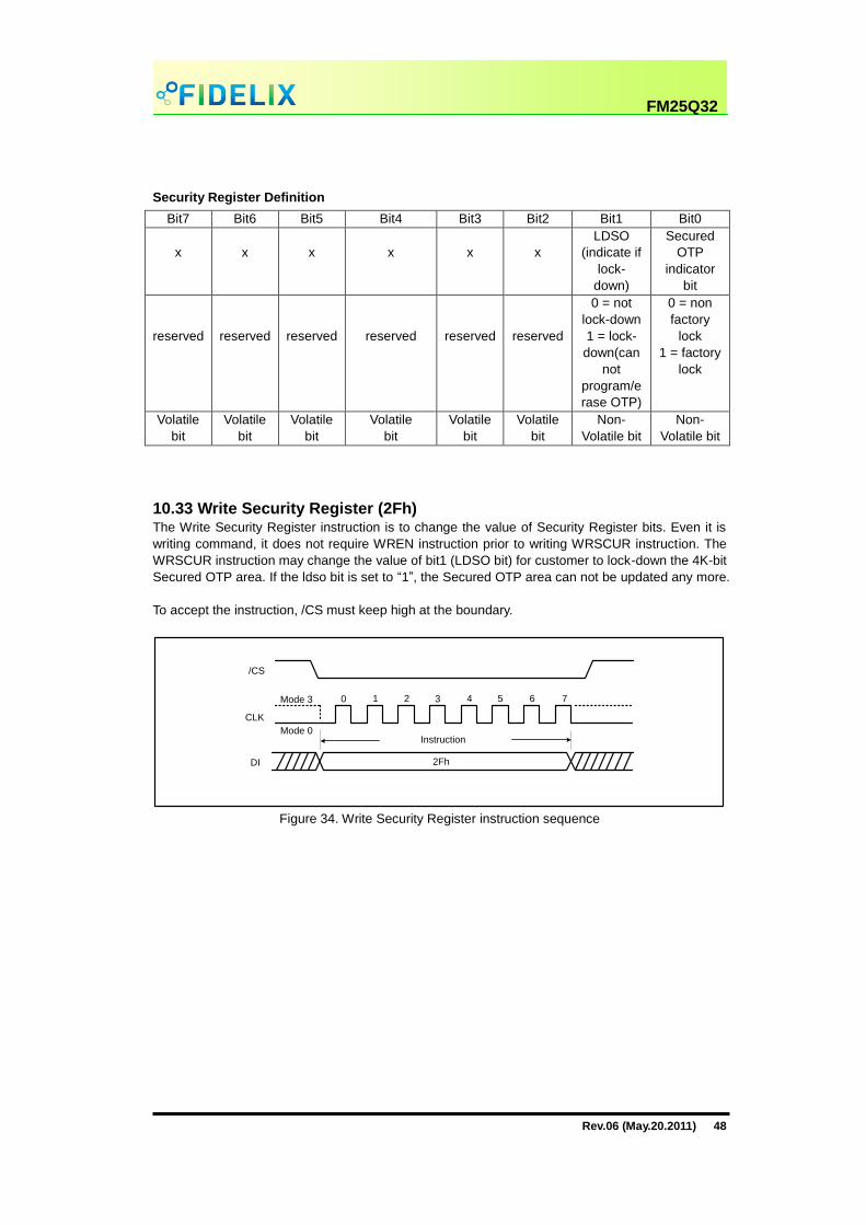
Rev.06 (May.20.2011) 48
FM25Q32
Security Register Definition
Bit7 Bit6 Bit5 Bit4 Bit3 Bit2 Bit1 Bit0
x
x
x
x
x
x
LDSO
(indicate if
lock-
down)
Secured
OTP
indicator
bit
reserved
reserved
reserved
reserved
reserved
reserved
0 = not
lock-down
1 = lock-
down(can
not
program/e
rase OTP)
0 = non
factory
lock
1 = factory
lock
Volatile
bit
Volatile
bit
Volatile
bit
Volatile
bit
Volatile
bit
Volatile
bit
Non-
Volatile bit
Non-
Volatile bit
10.33 Write Security Register (2Fh) The Write Security Register instruction is to change the value of Security Register bits. Even it is
writing command, it does not require WREN instruction prior to writing WRSCUR instruction. The
WRSCUR instruction may change the value of bit1 (LDSO bit) for customer to lock-down the 4K-bit
Secured OTP area. If the ldso bit is set to “1”, the Secured OTP area can not be updated any more.
To accept the instruction, /CS must keep high at the boundary.
Mode 0
Mode 3
Instruction
DI
CLK
/CS
6543 70 1 2
2Fh
Figure 34. Write Security Register instruction sequence

Rev.06 (May.20.2011) 49
FM25Q32
10.34 Set Burst with Wrap (77h) The Set Burst with Wrap (77h) instruction is to define Burst length 8/16/32/64-byte section within
a 256-byte page in “Fast Read Quad I/O”.
Similar to a Quad I/O instruction, the Set Burst with Wrap instruction is initiated by driving the /CS
pin low and then sending the instruction code “77h” with following 24 dummy bits and 8 “Wrap Bits”,
W7-0. The instruction sequence is shown in Set Burst with Wrap Instruction Sequence.
Wrap bit W7 and the lower nibble W3-0 are not used.
W6, W5 W4 = 0 W4 = 1(Default)
Wrap Around Wrap Length Wrap Around Wrap Length
0 0 Yes 8-byte No N/A
0 1 Yes 16-byte No N/A
1 0 Yes 32-byte No N/A
1 1 Yes 64-byte No N/A
Once W6-4 is set by a Set Burst with Wrap instruction, all the following “Fast Read Quad I/O” and
instructions will use the W6-4 setting to access the 8/16/32/64-byte section within any page. To exit
the “Wrap Around” function and return to normal read operation, it is require to issue another Set
Burst with Wrap instruction with setting W4 = 1. The default value of W4 upon power on is W4=1.
If a system reset under Wrap Around mode with W4=0, issuing a Set Burst with Wrap instruction
with W4=1 is recommended prior to any normal Read instructions as FM25Q32 does not have a
hardware Reset Pin.
Mode 0
Mode 3
77h
CLK
/CS
6543 70 1 2
High - Z
1312108 9 14 15
Instruction
IO0
IO1
IO2
IO3
High - Z
High - Z
Don’t care
X X w4
X X w5
X X w6
X X X
X
X
X
X
Wrap
bit
X X X
X X X
X X X
X X X
X
X
X
X
Don’t care
Don’t care
11
Figure 35. Set Burst with Wrap Instruction Sequence
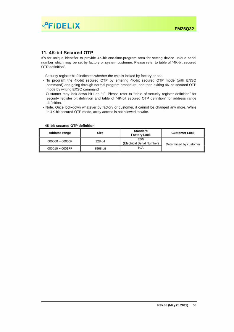
Rev.06 (May.20.2011) 50
FM25Q32
11. 4K-bit Secured OTP It’s for unique identifier to provide 4K-bit one-time-program area for setting device unique serial
number which may be set by factory or system customer. Please refer to table of “4K-bit secured
OTP definition”.
- Security register bit 0 indicates whether the chip is locked by factory or not.
- To program the 4K-bit secured OTP by entering 4K-bit secured OTP mode (with ENSO
command) and going through normal program procedure, and then exiting 4K-bit secured OTP
mode by writing EXSO command
- Customer may lock-down bit1 as “1”. Please refer to “table of security register definition” for
security register bit definition and table of “4K-bit secured OTP definition” for address range
definition.
- Note. Once lock-down whatever by factory or customer, it cannot be changed any more. While
in 4K-bit secured OTP mode, array access is not allowed to write.
4K-bit secured OTP definition
Address range Size Standard
Factory Lock Customer Lock
000000 ~ 00000F 128-bit ESN
(Electrical Serial Number) Determined by customer
000010 ~ 0001FF 3968-bit N/A

Rev.06 (May.20.2011) 51
FM25Q32
12. ELECTRICAL CHARACTERISTICS
12.1 Absolute Maximum Ratings (1)
PARAMETERS SYMBOL CONDITIONS RANGE UNIT
Supply Voltage VCC -0.6 to +4.0 V
Voltage Applied to Any Pin VIO Relative to Ground -0.6 to VCC +0.4 V
Transient Voltage on any Pin VIOT <20nS Transient
Relative to Ground
-2.0V to VCC +2.0V V
Storage Temperature TSTG -65 to +150 ˚C
Lead Temperature TLEAD See Note(3)
˚C
Electrostatic Discharge
Voltage
VESD Human
Body Model(4)
-2000 to +2000 V
Notes:
1. Specification for FM25Q32 is preliminary. See preliminary designation at the end of this
document.
2. This device has been designed and tested for the specified operation ranges. Proper operation
outside of these levels is not guaranteed. Exposure to absolute maximum ratings may affect
device reliability. Exposure beyond absolute maximum ratings may cause permanent damage.
3. Compliant with JEDEC Standard J-STD-20C for small body Sn-Pb or Pb-free (Green) assembly
and the European directive on restrictions on hazardous substances (RoHS) 2002/95/EU.
4. JEDEC Std JESD22-A114A (C1=100pF, R1=1500 ohms, R2=500 ohms).
12.2 Operating Ranges
PARAMETER SYMBOL CONDITIONS MIN MAX UNIT
Erase/Program
Cycles
VCC FR1 = 85MHz (Single/Dual/Quad SPI)
FR2 = 104MHz (Single/Dual/Quad SPI)
fR = 50MHz (Read Data 03h)
2.7
3.0
2.7
3.6 V
Temperature,Op
erating Tj Industrial -40 +85 ˚C

Rev.06 (May.20.2011) 52
FM25Q32
12.3 Endurance and Data Retention
PARAMETER CONDITIONS MIN MAX UNIT
Erase/Program Cycles 4KB sector, 32/64KB block or full chip. 100,000 Cycles
Data Retention Full Temperature Range 20 years
12.4 Power-up Timing and Write Inhibit Threshold
PARAMETER SYMBOL SPEC
UNIT MIN MAX
VCC(min) to /CS Low tVSL(1)
10 ㎲
Time Delay Before Write Instruction tPUW(1)
1 10 ㎳
Write Inhibit Threshold Voltage VWI(1)
1 2 V
Note:
1. These parameters are characterized only.
VCC(max)
VCC(min)
VWI
VCC
Program. Erase and Write Instructions are Ignored
/CS Must Track VCC
tVSL Read InstructionsAllowed
Device is FullyAccessible
tPUW
ResetState
Time
VCC(max)
VCC(min)
VWI
VCC
Program. Erase and Write Instructions are Ignored
/CS Must Track VCC
tVSL Read InstructionsAllowed
Device is FullyAccessible
tPUW
ResetState
Time
Figure 36. Power-up Timing and Voltage Levels

Rev.06 (May.20.2011) 53
FM25Q32
12.5 DC Electrical Characteristics
PARAMETER SYMBOL CONDITION SPEC
UNIT MIN TYP MAX
Input Capacitance CIN(1)
VIN=0V(2)
6 ㎊
Output Capacitance COUT(1)
VOUT=0V(2)
8 ㎊
Input Leakage ILI ±2 ㎂
I/O Leakage ILO ±2 ㎂
Standby Current ICC1
/CS=VCC,
VIN=GND or VCC 10 50 ㎂
Deep Power-down
Current ICC2
/CS=VCC,
VIN=GND or VCC 3 10 ㎂
Current Read Data/
Dual/Quad 1㎒(2)
ICC3
C=0.1 VCC / 0.9VCC
IO=Open 4/5/6 6/7.5/9 ㎃
Current Read Data/
Dual/Quad 33㎒(2)
ICC3
C=0.1 VCC / 0.9VCC
IO=Open 6/7/8 9/10.5/12 ㎃
Current Read Data/
Dual/Quad 50㎒(2)
ICC3
C=0.1 VCC / 0.9VCC
IO=Open 7/8/9 10/12/13.5 ㎃
Current Read Data/
Dual/Quad 85㎒(2)
ICC3
C=0.1 VCC / 0.9VCC
IO=Open 10/11/12 15/16.5/18 ㎃
Current Write
Status Register ICC4 /CS=VCC 10 18 ㎃
Current page
Program ICC5 /CS=VCC 20 25 ㎃
Current Sector/Block
Erase ICC6 /CS=VCC 20 25 ㎃
Current Chip Erase ICC7 /CS=VCC 20 25 ㎃
Input Low Voltages VIL -0.5 VCC x0.2 V
Input High Voltages VIH VCC x0.8 VCC +0.4 V
Output Low Voltages VOL IOL=1.6㎃ 0.4 V
Output
High Voltages VOH IOH=-100㎂ VCC -0.2 V
Notes:
1. Tested on sample basis and specified through design and characterization data, TA = 25˚C,
VCC = 3V.
2. Checked Board Pattern.

Rev.06 (May.20.2011) 54
FM25Q32
12.6 AC Measurement Conditions
PARAMETER SYMBOL SPEC
UNIT MIN MAX
Load Capacitance CL 30 ㎊
Input Rise and Fall Times TR, TF 5 ㎱
Input Pulse Voltages VIN 0.2 VCC to O. 8 VCC V
Input Timing Reference Voltages IN 0.3 VCC to O. 7 VCC V
Output Timing Reference Voltages OUT 0.5 VCC to O. 5 VCC V
Note:
1. Output Hi-Z is defined as the point where data out is no longer driven.
0.5 VCC
0.8 VCC
0.2 VCC
Input LevelsInput and Output
Timing Reference Levels
0.5 VCC
0.8 VCC
0.2 VCC
Input LevelsInput and Output
Timing Reference Levels
0.5 VCC
0.8 VCC
0.2 VCC
Input LevelsInput and Output
Timing Reference Levels
Figure 37. AC Measurement I/O Waveform
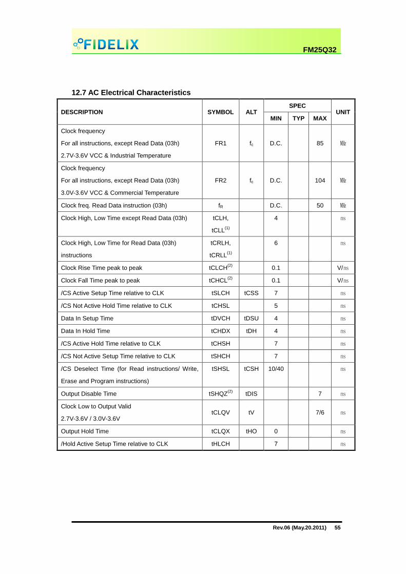
Rev.06 (May.20.2011) 55
FM25Q32
12.7 AC Electrical Characteristics
DESCRIPTION SYMBOL ALT SPEC
UNIT MIN TYP MAX
Clock frequency
For all instructions, except Read Data (03h)
2.7V-3.6V VCC & Industrial Temperature
FR1 fc D.C. 85 ㎒
Clock frequency
For all instructions, except Read Data (03h)
3.0V-3.6V VCC & Commercial Temperature
FR2 fc D.C. 104 ㎒
Clock freq. Read Data instruction (03h) fR D.C. 50 ㎒
Clock High, Low Time except Read Data (03h) tCLH,
tCLL(1)
4 ㎱
Clock High, Low Time for Read Data (03h)
instructions
tCRLH,
tCRLL(1)
6 ㎱
Clock Rise Time peak to peak tCLCH(2)
0.1 V/㎱
Clock Fall Time peak to peak tCHCL(2)
0.1 V/㎱
/CS Active Setup Time relative to CLK tSLCH tCSS 7 ㎱
/CS Not Active Hold Time relative to CLK tCHSL 5 ㎱
Data In Setup Time tDVCH tDSU 4 ㎱
Data In Hold Time tCHDX tDH 4 ㎱
/CS Active Hold Time relative to CLK tCHSH 7 ㎱
/CS Not Active Setup Time relative to CLK tSHCH 7 ㎱
/CS Deselect Time (for Read instructions/ Write,
Erase and Program instructions)
tSHSL tCSH 10/40 ㎱
Output Disable Time tSHQZ(2)
tDIS 7 ㎱
Clock Low to Output Valid
2.7V-3.6V / 3.0V-3.6V tCLQV tV 7/6 ㎱
Output Hold Time tCLQX tHO 0 ㎱
/Hold Active Setup Time relative to CLK tHLCH 7 ㎱
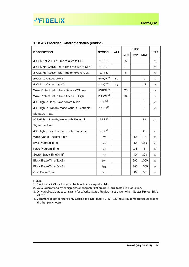
Rev.06 (May.20.2011) 56
FM25Q32
12.8 AC Electrical Characteristics (cont’d)
DESCRIPTION SYMBOL ALT SPEC
UNIT MIN TYP MAX
/HOLD Active Hold Time relative to CLK tCHHH 5 ㎱
/HOLD Not Active Setup Time relative to CLK tHHCH 7 ㎱
/HOLD Not Active Hold Time relative to CLK tCHHL 5 ㎱
/HOLD to Output Low-Z tHHQX(2)
tLZ 7 ㎱
/HOLD to Output High-Z tHLQZ(2)
tHZ 12 ㎱
Write Protect Setup Time Before /CS Low tWHSL(3)
20 ㎱
Write Protect Setup Time After /CS High tSHWL(3)
100 ㎱
/CS High to Deep Power-down Mode tDP(2)
3 ㎲
/CS High to Standby Mode without Electronic
Signature Read
tRES1(2)
3 ㎲
/CS High to Standby Mode with Electronic
Signature Read
tRES2(2)
1.8 ㎲
/CS High to next Instruction after Suspend tSUS(2)
20 ㎲
Write Status Register Time tw 10 15 ㎳
Byte Program Time
tBP 10 150 ㎲
Page Program Time tPP 1.5 5 ㎳
Sector Erase Time(4KB) tSE 40 300 ㎳
Block Erase Time(32KB) tBE1 200 1000 ㎳
Block Erase Time(64KB) tBE2 300 1500 ㎳
Chip Erase Time tCE 16 50 s
Notes:
1. Clock high + Clock low must be less than or equal to 1/fc.
2. Value guaranteed by design and/or characterization, not 100% tested in production.
3. Only applicable as a constraint for a Write Status Register instruction when Sector Protect Bit is
set to 1.
4. Commercial temperature only applies to Fast Read (FR1 & FR2). Industrial temperature applies to
all other parameters.
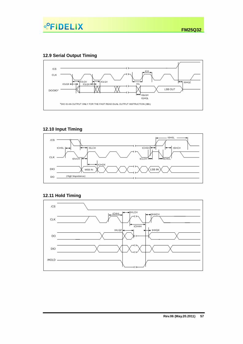
Rev.06 (May.20.2011) 57
FM25Q32
12.9 Serial Output Timing
12.10 Input Timing
12.11 Hold Timing
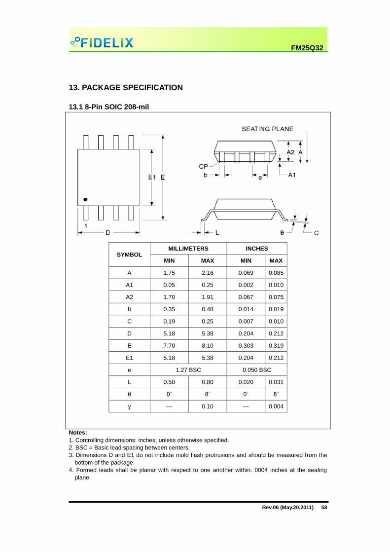
Rev.06 (May.20.2011) 58
FM25Q32
13. PACKAGE SPECIFICATION
13.1 8-Pin SOIC 208-mil
SYMBOL MILLIMETERS INCHES
MIN MAX MIN MAX
A 1.75 2.16 0.069 0.085
A1 0.05 0.25 0.002 0.010
A2 1.70 1.91 0.067 0.075
b 0.35 0.48 0.014 0.019
C 0.19 0.25 0.007 0.010
D 5.18 5.38 0.204 0.212
E 7.70 8.10 0.303 0.319
E1 5.18 5.38 0.204 0.212
e 1.27 BSC 0.050 BSC
L 0.50 0.80 0.020 0.031
θ 0˚ 8˚ 0˚ 8˚
y --- 0.10 --- 0.004
Notes:
1. Controlling dimensions: inches, unless otherwise specified.
2. BSC = Basic lead spacing between centers.
3. Dimensions D and E1 do not include mold flash protrusions and should be measured from the
bottom of the package.
4. Formed leads shall be planar with respect to one another within. 0004 inches at the seating
plane.

Rev.06 (May.20.2011) 59
FM25Q32
13.2 8-Pin VSOP 208-mil
SYMBOL MILLIMETERS INCHES
MIN TYP. MAX IN TYP. MAX
A --- --- 1.00 --- --- 0.039
A1 0.05 0.10 0.15 0.002 0.004 0.006
A2 0.75 0.80 0.85 0.030 0.031 0.033
b 0.35 0.42 0.48 0.014 0.017 0.019
c
0.127 REF. 0.005 REF.
D 5.18 5.28 5.38 0.204 0.208 0.212
E 7.70 7.90 8.10 0.303 0.311 0.319
E1
5.18 5.28 5.38 0.204 0.208 0.212
e
--- 1.27 --- --- 0.050 ---
L 0.50 0.65 0.80 0.020 0.026 0.031
y --- --- 0.10 --- --- 0.004
θ 0 ˚ --- 8 ˚ 0 ˚ --- 8 ˚
Notes:
1. JEDEC outline : N/A.
2. Dimension “D”, “D1” does not include mold flash, mold flash shall not exceed 0.006 [0.15mm]
per end. Dimension “E”, “E1” does not include inter lead flash. Inter lead flash shall not exceed
0.010 [0.25mm] per side.
3. Dimension “b” does not include dambar protrusion. Allowable dambar protrusion shall be 0.003
[0.08mm].
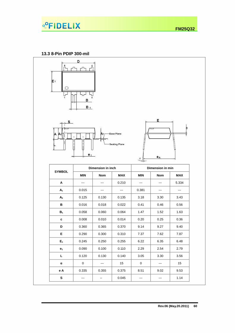
Rev.06 (May.20.2011) 60
FM25Q32
13.3 8-Pin PDIP 300-mil
SYMBOL Dimension in inch Dimension in min
MIN Nom MAX MIN Nom MAX
A --- --- 0.210 --- --- 5.334
A1 0.015 --- --- 0.381 --- ---
A2 0.125 0.130 0.135 3.18 3.30 3.43
B 0.016 0.018 0.022 0.41 0.46 0.56
B1 0.058 0.060 0.064 1.47 1.52 1.63
c 0.008 0.010 0.014 0.20 0.25 0.36
D 0.360 0.365 0.370 9.14 9.27 9.40
E 0.290 0.300 0.310 7.37 7.62 7.87
E1 0.245 0.250 0.255 6.22 6.35 6.48
e1 0.090 0.100 0.110 2.29 2.54 2.79
L 0.120 0.130 0.140 3.05 3.30 3.56
α 0 --- 15 0 --- 15
e A 0.335 0.355 0.375 8.51 9.02 9.53
S --- -- 0.045 --- --- 1.14

Rev.06 (May.20.2011) 61
FM25Q32
13.4 8-contact 6x5 WSON
SYMBOL MILLIMETERS INCHES
MIN TYP. MAX IN TYP. MAX
A 0.70 0.75 0.80 0.0276 0.0295 0.0315
A1 0.00 0.02 0.05 0.0000 0.0008 0.0019
A2 0.55 0.0126
A3 0.19 0.20 0.25 0.0075 0.0080 0.0098
b 0.36 0.40 0.48 0.0138 0.0157 0.0190
D(3)
5.90 6.00 6.10 0.2320 0.2360 0.2400
D1 3.30 3.40 3.50 0.1299 0.1338 0.1377
E 4.90 5.00 5.10 0.1930 0.1970 0.2010
E1(3)
4.20 4.30 4.40 0.1653 0.1692 0.1732
e(2)
1.27 BSC 0.0500 BSC
K 0.20 0.0080
L 0.50 0.60 0.75 0.0197 0.0236 0.0295

Rev.06 (May.20.2011) 62
FM25Q32
13.5 8-contact 6x5 WSON Cont’d
SYMBOL MILLIMETERS INCHES
MIN TYP. MAX MIN TYP. MAX
SOLDER PATTERN
M 3.40 0.1338
N 4.30 0.1692
P 6.00 0.2360
Q 0.50 0.0196
R 0.75 0.0255
Notes:
1. Advanced Packaging Information; please contact Fidelix Co., Ltd. for the latest minimum and
maximum specifications.
2. BSC = Basic lead spacing between centers.
3. Dimensions D and E1 do not include mold flash protrusions and should be measured from the bottom
of the package.
4. The metal pad area on the bottom center of the package is connected to the device ground (GND
pin). Avoid placement of exposed PCB bias under the pad.

Rev.06 (May.20.2011) 63
FM25Q32
13.6 16-Pin SOIC 300-mil
SYMBOL MILLIMETERS INCHES
MIN MAX MIN MAX
A 2.36 2.64 0.093 0.104
A1 0.10 0.30 0.005 0.012
b 0.33 0.51 0.013 0.020
C 0.18 0.28 0.007 0.000
D(3)
10.08 10.49 0.397 0.413
E 10.01 10.64 0.394 0.419
E1(3)
7.39 7.59 0.291 0.299
e(2)
1.27BSC 0.050
L 0.39 1.27 0.015 0.050
θ 0˚ 8˚ 0˚ 8˚
y --- 0.076 --- 0.003
Notes:
1. Controlling dimensions: inches, unless otherwise specified.
2. BSC = Basic lead spacing between centers.
3. Dimensions D and E1 do not include mold flash protrusions and should be measured from the
bottom of the package.
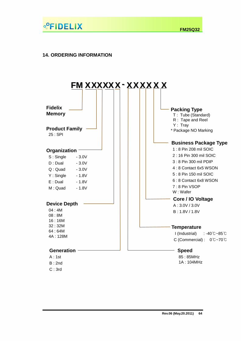
Rev.06 (May.20.2011) 64
FM25Q32
14. ORDERING INFORMATION
FM
Fidelix
Memory
Product Family25 : SPI
Organization
S : Single - 3.0V
D : Dual - 3.0V
Q : Quad - 3.0V
Y : Single - 1.8V
E : Dual - 1.8V
M : Quad - 1.8V
Device Depth
04 : 4M
08 : 8M
16 : 16M
32 : 32M
64 : 64M
4A : 128M
Business Package Type
1 : 8 Pin 208 mil SOIC
2 : 16 Pin 300 mil SOIC
3 : 8 Pin 300 mil PDIP
4 : 8 Contact 6x5 WSON
5 : 8 Pin 150 mil SOIC
6 : 8 Contact 6x8 WSON
7 : 8 Pin VSOP
W : Wafer
Speed
85 : 85MHz
1A : 104MHz
Packing TypeT : Tube (Standard)
R : Tape and Reel
Y : Tray
* Package NO Marking
XXXXXX XX X X X
Temperature
I (Industrial) : -40℃~85℃
C (Commercial) : 0℃~70℃
X
Core / IO Voltage
A : 3.0V / 3.0V
B : 1.8V / 1.8V
Generation
A : 1st
B : 2nd
C : 3rd
-
![MILAN unmanaged switch MIL-S8TA Unmanaged Switches ......Specifications Physical Characteristics Enclosure Case Rugged metal chassis Dimensions Width: 6.5” [165 mm] Depth: 4.0”](https://static.fdocuments.in/doc/165x107/6076b9bfb6c52a226500d359/milan-unmanaged-switch-mil-s8ta-unmanaged-switches-specifications-physical.jpg)