Floating Capacitance Multiplier Circuit Using Full ... · floating capacitance multiplier circuit...
4
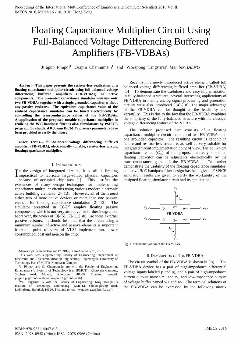
Abstract—This paper presents the resistor-less realization of a floating capacitance multiplier circuit using full-balanced voltage differencing buffered amplifiers (FB-VDBAs) as active components. The presented capacitance simulator contains only two FB-VDBAs together with a single grounded capacitor without any passive resistors. The equivalent capacitance value of the realized capacitance simulator can be tuned electronically by controlling the transconductance values of the FB-VDBAs. Anapplication of the proposed tunable capacitance multiplier in realizing the RLC bandpass filter is also. Simulations by PSPICE program for standard 0.35-μm BiCMOS process parameter shave been provided to verify the theory. Index Terms— full-balanced voltage differencing buffered amplifier (FB-VDBA), electronically tunable, resistor-less circuit, floatingcapacitance multiplier. I. INTRODUCTION n the design of integrated circuits, it is still a limiting impractical to fabricate large-valued physical capacitors because of occupied chip area [1]. This justifies the existences of many design techniques for implementing capacitance multiplier circuits using various modern electronic active building elements [2]-[13]. However, all of them need either two of more active devices or more than one passive element for floating capacitance simulation [2]-[13]. The simulator presented in [3]-[7] employ floating passive components, which is not very attractive for further integration. Moreover, the works of [3]-[5], [7]-[11] still use some external passive resistors. It should be noted that the circuit using a minimum number of active and passive elements is important from the point of view of VLSI implementation, power consumption, cost and area on the chip. Manuscript received January 12, 2016; revised January 19, 2016. This work was supported by Faculty of Engineering, Department of Electronic and Telecommunication Engineering, Rajamangala University of Technology Isan (RMUTI), Khonkaen Campus. 1 J. Pimpol and O. Channumsin are with the Faculty of Engineering, Rajamangala University of Technology Isan (RMUTI), Khonkaen Campus., Srichan road, Muang, KhonKaen 40000, Thailand (e-mail: [email protected] and [email protected]). 2 W. Tangsrirat is with the Faculty of Engineering, King Mongkut’s Institute of Technology Ladkrabang (KMITL), Chalongkrung road, Ladkrabang, Bangkok 10520, Thailand (e-mail: [email protected]). Recently, the newly introduced active element called full balanced voltage differencing buffered amplifier (FB-VDBA) [14]. To demonstrate the usefulness and easy implementation in fully-balanced structures, several interesting applications of FB-VDBA in mainly analog signal processing and generation circuits were also introduced [14]-[18]. The major advantage of the FB-VDBA can be thought as the feasibility and versatility. This is due to the fact that the FB-VDBA combines the simplicity of the fully-balanced structure with the classical voltage differencing feature of the VDBA. The solution proposed here consists of a floating capacitance multiplier circuit made up of two FB-VDBAs and one grounded capacitor. The resulting circuit is canonic in nature and resistor-less structure, as well as very suitable for integrated circuit implementation point of view. The equivalent capacitance value (Ceq) of the proposed actively simulated floating capacitor can be adjustable electronically by the transconductance gains of the FB-VDBAs. To further demonstrate the usability of the floating capacitance simulator, an active RLC bandpass filter design has been given. PSPICE simulation results are given to verify the workability of the designed floating simulator circuit and its application. v p v w+ v w- w+ w- p FB-VDBA v n n v z+ i z+ z+ v z- i z- z- Fig. 1 Schematic symbol of the FB-VDBA. II. DESCRIPTION OF THE FB-VDBA The circuit symbol of the FB-VDBA is shown in Fig. 1. The FB-VDBA device has a pair of high-impedance differential voltage inputs labeled p and n), and a pair of high-impedance current outputs named z+ and z-, and low-impedance outputs of voltage buffer named w+ and w-. The terminal relations of the FB-VDBA can be expressed by the following matrix Floating Capacitance Multiplier Circuit Using Full-Balanced Voltage Differencing Buffered Amplifiers (FB-VDBAs) Jirapun Pimpol 1 Orapin Channumsin 1 and Worapong Tangsrirat 2 , Member, IAENG I Proceedings of the International MultiConference of Engineers and Computer Scientists 2016 Vol II, IMECS 2016, March 16 - 18, 2016, Hong Kong ISBN: 978-988-14047-6-3 ISSN: 2078-0958 (Print); ISSN: 2078-0966 (Online) IMECS 2016
Transcript of Floating Capacitance Multiplier Circuit Using Full ... · floating capacitance multiplier circuit...
Abstract—This paper presents the resistor-less realization of a
floating capacitance multiplier circuit using full-balanced voltage
differencing buffered amplifiers (FB-VDBAs) as active
components. The presented capacitance simulator contains only
two FB-VDBAs together with a single grounded capacitor without
any passive resistors. The equivalent capacitance value of the
realized capacitance simulator can be tuned electronically by
controlling the transconductance values of the FB-VDBAs.
Anapplication of the proposed tunable capacitance multiplier in
realizing the RLC bandpass filter is also. Simulations by PSPICE
program for standard 0.35-µm BiCMOS process parameter shave
been provided to verify the theory.
Index Terms— full-balanced voltage differencing buffered
amplifier (FB-VDBA), electronically tunable, resistor-less circuit,
floatingcapacitance multiplier.
I. INTRODUCTION
n the design of integrated circuits, it is still a limiting impractical to fabricate large-valued physical capacitors because of occupied chip area [1]. This justifies the
existences of many design techniques for implementing capacitance multiplier circuits using various modern electronic active building elements [2]-[13]. However, all of them need either two of more active devices or more than one passive element for floating capacitance simulation [2]-[13]. The simulator presented in [3]-[7] employ floating passive components, which is not very attractive for further integration. Moreover, the works of [3]-[5], [7]-[11] still use some external passive resistors. It should be noted that the circuit using a minimum number of active and passive elements is important from the point of view of VLSI implementation, power consumption, cost and area on the chip.
Manuscript received January 12, 2016; revised January 19, 2016.
This work was supported by Faculty of Engineering, Department of
Electronic and Telecommunication Engineering, Rajamangala University of
Technology Isan (RMUTI), Khonkaen Campus. 1J. Pimpol and O. Channumsin are with the Faculty of Engineering,
Rajamangala University of Technology Isan (RMUTI), Khonkaen Campus.,
Srichan road, Muang, KhonKaen 40000, Thailand (e-mail:
[email protected] and [email protected]). 2W. Tangsrirat is with the Faculty of Engineering, King Mongkut’s
Institute of Technology Ladkrabang (KMITL), Chalongkrung road,
Ladkrabang, Bangkok 10520, Thailand (e-mail: [email protected]).
Recently, the newly introduced active element called full balanced voltage differencing buffered amplifier (FB-VDBA) [14]. To demonstrate the usefulness and easy implementation in fully-balanced structures, several interesting applications of FB-VDBA in mainly analog signal processing and generation circuits were also introduced [14]-[18]. The major advantage of the FB-VDBA can be thought as the feasibility and versatility. This is due to the fact that the FB-VDBA combines the simplicity of the fully-balanced structure with the classical voltage differencing feature of the VDBA.
The solution proposed here consists of a floating capacitance multiplier circuit made up of two FB-VDBAs and one grounded capacitor. The resulting circuit is canonic in nature and resistor-less structure, as well as very suitable for integrated circuit implementation point of view. The equivalent capacitance value (Ceq) of the proposed actively simulated floating capacitor can be adjustable electronically by the transconductance gains of the FB-VDBAs. To further demonstrate the usability of the floating capacitance simulator, an active RLC bandpass filter design has been given. PSPICE simulation results are given to verify the workability of the designed floating simulator circuit and its application.
vp vw+
vw-
w+
w-
p
FB-VDBA
vn n
vz+
iz+
z+
vz-
iz-
z-
Fig. 1 Schematic symbol of the FB-VDBA.
II. DESCRIPTION OF THE FB-VDBA
The circuit symbol of the FB-VDBA is shown in Fig. 1. The
FB-VDBA device has a pair of high-impedance differential
voltage inputs labeled p and n), and a pair of high-impedance
current outputs named z+ and z-, and low-impedance outputs
of voltage buffer named w+ and w-. The terminal relations of
the FB-VDBA can be expressed by the following matrix
Floating Capacitance Multiplier Circuit Using
Full-Balanced Voltage Differencing Buffered
Amplifiers (FB-VDBAs)
Jirapun Pimpol1 Orapin Channumsin1 and Worapong Tangsrirat2, Member, IAENG
I
Proceedings of the International MultiConference of Engineers and Computer Scientists 2016 Vol II, IMECS 2016, March 16 - 18, 2016, Hong Kong
ISBN: 978-988-14047-6-3 ISSN: 2078-0958 (Print); ISSN: 2078-0966 (Online)
IMECS 2016

equation [14] :
z
z
n
p
mm
mm
w
w
z
z
v
v
v
v
gg
gg
v
v
i
i
.
1000
0100
00
00
(1)
where the parameter gm implies the transconductance gain of
the FB-VDBA. In Eq.(10), the gm-value is possible to control
electronically via the external supplied current or voltage.
Recently, the possible realization of the FB-VDBA in
BiCMOS technology is introduced. Fig. 2 shows the internal
BiCMOS structure of the recently introduced FB-VDBA [18].
It is designed by combining bipolar and CMOS technologies in
order to utilize the main advantages of each technology, i.e.,
higher transconductance, higher frequency, low power
consumption, and small silicon area. The FB-VDBA in Fig.2
is a combination of the transconductance amplifier as the input
stage (M1-M2, Q1-Q4), the mirror stages (Q5-Q7, Q8-Q10, Q11-
Q12 and Q13-Q14) transfer the current to ports z+ and z-,
respectively, and the unity-gain voltage buffer as the output
stage (M3-M6 and M7-M10). The small-signal effective
transconductance (gm) of the FB-VDBA can be written as :
T
Bm
V
Ig (2)
Where VT 26 mV at 27 C is the thermal voltage. Eq.(2)
indicates that the gm-value of the realized FB-VDBA is tunable
linearly and electronically by an external DC bias current IB.
Moreover, if we assume all the transistors operate in the
active region. Therefore, the elective small-signal voltage
gains in Fig. 2 are approximately to :
54
63
gg
gg
v
v
z
w (3)
and
108
97
gg
gg
v
v
z
w (4)
where gi denotes the conductance of transistor Mi (i = 1,
2,..,10). Assume that all the transistors have the same gi-
values, thus vw+ vz and vw- vz as expected.
III. PROPOSED FLOATING CAPACITANCE MULTIPLIER
The proposed floating capacitance simulator circuitusing
FB-VDBAs as active elements is shown in Fig. 3. The
proposed floating inductor constructionly two FB-VDBAs and
one grounded capacitor without external passive resistor
requirement,thus, the floatingcapacitoriscanonical structure and
also more suitablefor integrated circuit implementation point of
view.Circuit calculation of the proposed circuit in Fig. 3 shows
that the input impedance is equal to :
21
121
m
m
C
ingsC
g
i
vvZ
(5)
where the parameter gmi denotes the transconductance value of
i-th FB-VDBA (i = 1, 2).
M4
+V
iz+ z+
Q5
-V
M2M1n p
IB
IA IA
IB
Q3 Q4Q1 Q2
M3
w+
M5
M6Q8
Q9 Q10
Q7
Q6
Q13Q14
Q11 Q12
M8
M7
w-
M9
M10
izz-
Fig. 2 BiCMOS realization of the FB-VDBA [18].
Proceedings of the International MultiConference of Engineers and Computer Scientists 2016 Vol II, IMECS 2016, March 16 - 18, 2016, Hong Kong
ISBN: 978-988-14047-6-3 ISSN: 2078-0958 (Print); ISSN: 2078-0966 (Online)
IMECS 2016

Eq.(5) indicates that the proposed circuit can simulate a
floating capacitor with an equivalent capacitance Ceq:
1
21
m
meq
g
gCC (6)
It is to be noted form eq.(5) that the Ceq–value is adjustable
electronically by tuning gm1 and/or gm2.
z-
w-
FB-VDBA
iC
z+
p
1
v1
p
n
FB-VDBA
z+
w+
2iC
v2
w+
z-
n
w-
C1
Fig. 3 Proposed actively floating capacitance multiplier circuit.
IV. CIRCUIT PERFORMANCE SIMULATIONS
The performance verification of the proposed FB-VDBA
realization in Fig. 3,the circuit was simulated on PSPICE
program. In simulations, the FB-VDBA given in Fig. 2 was
implemented with standard 0.35-µm BiCMOS process
parameters [18]. Transistor aspect ratios (W/L in µm/µm)
were selected as : 14/0.7 and 56/0.7 for M1-M2 and M3-M10,
respectively. The circuit was biased at : IA = 25 µA under
the supplied voltages of +V = -V = 1 V.
The simulation results of the proposed floating capacitor
in Fig. 3 are also performed with the following active and
passive components : C1 = 0.1 nF, gm2 1.92 mA/V (IB2
50 µA) and gm1 3.84 mA/V, 1.92 mA/V, 1.28 mA/V, (IB1
100 µA, 50 µA and 33 µA), to obtain Ceq = 0.05 nF, 0.1 nF
and 0.15 nF, respectively.
0 10 20 30 40
Time (µs)
-100
-50
0
50
100
-40
-20
0
20
40
Current
(µA)Voltage
(mV)
vin
iC
Fig. 4 Simulated transient responses for vin and iC of the floating inductor
in Fig. 3.
Fig. 4 depicts the simulated transient responses for vin (=
v1–v2) and iC of the input impedance of the proposed floating
capacitance simulator. The results obtained from the
simulation show that the current iC leads the voltage vin by
89.57. The simulated frequency characteristics of the input
impedance of the proposed inductor are shown in Fig. 5.
100M
Frequency (Hz)
100 1k 10k 100k 1M 10M100
10k
1M
100M
Simulated
Theory
Ceq = 0.05 nF
Ceq = 0.1 nF
Ceq = 0.15 nF
Man
gnit
ude
(W)
(a)
-180
-90
0
90
180
100M
Frequency (Hz)
100 1k 10k 100k 1M 10M
Simulated
Theory
Ceq = 0.05 nF Ceq = 0.15 nF
Ceq = 0.1 nF
Ph
ase
(deg
ree)
(b)
Fig. 5 Theoretical and simulated frequency responses of the proposed
floating capacitor circuit in Fig. 3.
(a) magnitude responses (b) phase responses
V. APPLICATION EXAMPLE
As example to demonstrate an application of the proposed
floating capacitor of Fig. 3, it is employed in the RLC
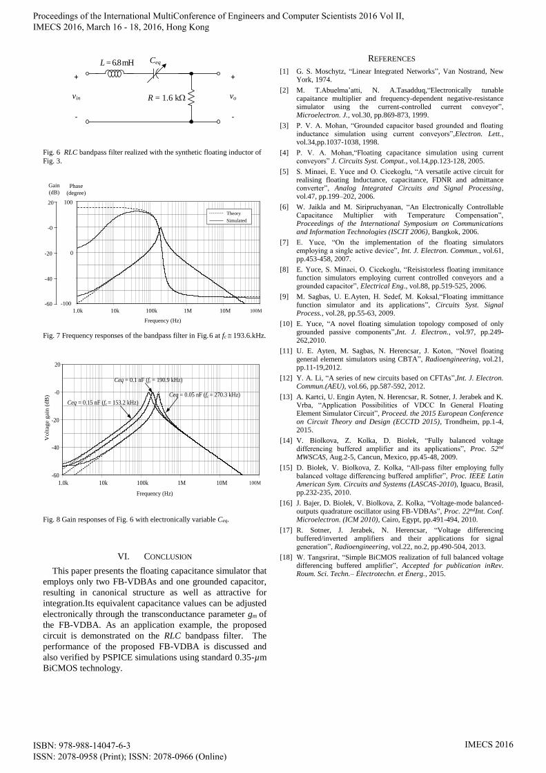
bandpass filter as shown in Fig. 6. The Ceq was selected as:
C1 = 0.1 nF and gm1 = gm2 1.92 mA/V (IB1 = IB2 50 µA)
for simulating Ceq 1 nF. Fig. 7 shows the idea and
simulated frequency responses of the bandpass filter in
Fig. 6. It appears, thus, that the simulated and ideal values
are in good agreement. In addition, in order to demonstrate
the electronic controllability of the proposed floating
inductor, the value of Ceq in Fig. 6 was respectively varied to
0.05 nF, 0.1 nF and 0.15 nF, by changing gm2 3.84 mA/V,
1.92 mA/V, 1.28 mA/V, respectively while keeping gm2
constant at 1.92 mA/V. This tuning leads to obtain the
center frequency fc 270 kHz, 190 kHz and 156 kHz,
respectively.
Proceedings of the International MultiConference of Engineers and Computer Scientists 2016 Vol II, IMECS 2016, March 16 - 18, 2016, Hong Kong
ISBN: 978-988-14047-6-3 ISSN: 2078-0958 (Print); ISSN: 2078-0966 (Online)
IMECS 2016
Ceq
vo
+
-
R = 1.6 kW
L = 6.8 mH
vin
+
-
Fig. 6 RLC bandpass filter realized with the synthetic floating inductor of
Fig. 3.
-60
-40
-20
-0
20
-100
0
100
Phase
(degree)
Gain
(dB)
1.0k 10k 100k 1M 10M 100M
Frequency (Hz)
Simulated
Theory
Fig. 7 Frequency responses of the bandpass filter in Fig. 6 at fc 193.6.kHz.
1.0k 10k 100k 1M 10M 100M
-60
-40
-20
-0
20
Frequency (Hz)
Volt
age g
ain
(dB
)
Ceq = 0.15 nF (fc = 153.2 kHz)
Ceq = 0.1 nF (fc = 190.9 kHz)
Ceq = 0.05 nF (fc = 270.3 kHz)
Fig. 8 Gain responses of Fig. 6 with electronically variable Ceq.
VI. CONCLUSION
This paper presents the floating capacitance simulator that
employs only two FB-VDBAs and one grounded capacitor,
resulting in canonical structure as well as attractive for
integration.Its equivalent capacitance values can be adjusted
electronically through the transconductance parameter gm of
the FB-VDBA. As an application example, the proposed
circuit is demonstrated on the RLC bandpass filter. The
performance of the proposed FB-VDBA is discussed and
also verified by PSPICE simulations using standard 0.35-µm
BiCMOS technology.
REFERENCES
[1] G. S. Moschytz, “Linear Integrated Networks”, Van Nostrand, New York, 1974.
[2] M. T.Abuelma’atti, N. A.Tasadduq,“Electronically tunable capaitance multiplier and frequency-dependent negative-resistance simulator using the current-controlled current conveyor”, Microelectron. J., vol.30, pp.869-873, 1999.
[3] P. V. A. Mohan, “Grounded capacitor based grounded and floating inductance simulation using current conveyors”,Electron. Lett., vol.34,pp.1037-1038, 1998.
[4] P. V. A. Mohan,“Floating capacitance simulation using current conveyors” J. Circuits Syst. Comput., vol.14,pp.123-128, 2005.
[5] S. Minaei, E. Yuce and O. Cicekoglu, “A versatile active circuit for realising floating Inductance, capacitance, FDNR and admittance converter”, Analog Integrated Circuits and Signal Processing, vol.47, pp.199–202, 2006.
[6] W. Jaikla and M. Siripruchyanan, “An Electronically Controllable Capacitance Multiplier with Temperature Compensation”, Proceedings of the International Symposium on Communications and Information Technologies (ISCIT 2006), Bangkok, 2006.
[7] E. Yuce, “On the implementation of the floating simulators employing a single active device”, Int. J. Electron. Commun., vol.61, pp.453-458, 2007.
[8] E. Yuce, S. Minaei, O. Cicekoglu, “Reisistorless floating immitance function simulators employing current controlled conveyors and a grounded capacitor”, Electrical Eng., vol.88, pp.519-525, 2006.
[9] M. Sagbas, U. E.Ayten, H. Sedef, M. Koksal,“Floating immittance function simulator and its applications”, Circuits Syst. Signal Process., vol.28, pp.55-63, 2009.
[10] E. Yuce, “A novel floating simulation topology composed of only grounded passive components”,Int. J. Electron., vol.97, pp.249-262,2010.
[11] U. E. Ayten, M. Sagbas, N. Herencsar, J. Koton, “Novel floating general element simulators using CBTA”, Radioengineering, vol.21, pp.11-19,2012.
[12] Y. A. Li, “A series of new circuits based on CFTAs”,Int. J. Electron. Commun.(AEU), vol.66, pp.587-592, 2012.
[13] A. Kartci, U. Engin Ayten, N. Herencsar, R. Sotner, J. Jerabek and K. Vrba, “Application Possibilities of VDCC In General Floating Element Simulator Circuit”, Proceed. the 2015 European Conference on Circuit Theory and Design (ECCTD 2015), Trondheim, pp.1-4, 2015.
[14] V. Biolkova, Z. Kolka, D. Biolek, “Fully balanced voltage differencing buffered amplifier and its applications”, Proc. 52nd MWSCAS, Aug.2-5, Cancun, Mexico, pp.45-48, 2009.
[15] D. Biolek, V. Biolkova, Z. Kolka, “All-pass filter employing fully balanced voltage differencing buffered amplifier”, Proc. IEEE Latin American Sym. Circuits and Systems (LASCAS-2010), Iguacu, Brasil, pp.232-235, 2010.
[16] J. Bajer, D. Biolek, V. Biolkova, Z. Kolka, “Voltage-mode balanced-outputs quadrature oscillator using FB-VDBAs”, Proc. 22ndInt. Conf. Microelectron. (ICM 2010), Cairo, Egypt, pp.491-494, 2010.
[17] R. Sotner, J. Jerabek, N. Herencsar, “Voltage differencing buffered/inverted amplifiers and their applications for signal generation”, Radioengineering, vol.22, no.2, pp.490-504, 2013.
[18] W. Tangsrirat, “Simple BiCMOS realization of full balanced voltage differencing buffered amplifier”, Accepted for publication inRev. Roum. Sci. Techn.– Électrotechn. et Énerg., 2015.
Proceedings of the International MultiConference of Engineers and Computer Scientists 2016 Vol II, IMECS 2016, March 16 - 18, 2016, Hong Kong
ISBN: 978-988-14047-6-3 ISSN: 2078-0958 (Print); ISSN: 2078-0966 (Online)
IMECS 2016