FlexRay ASSP MB88121B User’s Manual - Fujitsu Global PREFACE Purpose of this document Thank you...
266
FUJITSU SEMICONDUCTOR ASSP MANUAL FlexRay ASSP MB88121B User’s Manual AM15-11201-1E
Transcript of FlexRay ASSP MB88121B User’s Manual - Fujitsu Global PREFACE Purpose of this document Thank you...

FUJITSU SEMICONDUCTORASSP MANUAL
FlexRay ASSPMB88121B
User’s Manual
AM15-11201-1E


FUJITSU LIMITED
FlexRay ASSPMB88121B
User’s Manual


PREFACE
■ Purpose of this documentThank you for reading about this Fujitsu semiconductor device.
The MB88121B is a controller that performs FlexRay communications in accordance with the FlexRay
Protocol Specification Version 2.1.
This document is for engineers who are developing products that use the MB88121B, and explains the
registers, functions, and operation of the MB88121B. Read through the entire manual.
■ TrademarkFlexRay is a registered trademark of DaimlerChrysler AG.
The company names and brand names herein are the trademarks or registered trademarks of their respective
owners.
■ Reference DocumentsFlexRay Communications System Protocol Specification Version 2.1 (FlexRay Consortium)
■ Overall structure of this documentThis document consists of the following chapters.
CHAPTER 1 MB88121B
This chapter explains the features and basic specifications of the MB88121B.
CHAPTER 2 FlexRay
This chapter explains the functions and operations of FlexRay.
APPENDIX
These appendices explain the I/O registers and configuration parameters.
i

Copyright © 2007 FUJITSU LIMITED All rights reserved
• The contents of this document are subject to change without notice. Customers are advised to consult with FUJITSU sales representatives before ordering.
• The information, such as descriptions of function and application circuit examples, in this document are presented solely for the purpose of reference to show examples of operations and uses of FUJITSU semiconductor device; FUJITSU does not warrant proper operation of the device with respect to use based on such information. When you develop equipment incorporating the device based on such information, you must assume any responsibility arising out of such use of the information. FUJITSU assumes no liability for any damages whatsoever arising out of the use of the information.
• Any information in this document, including descriptions of function and schematic diagrams, shall not be construed as license of the use or exercise of any intellectual property right, such as patent right or copyright, or any other right of FUJITSU or any third party or does FUJITSU warrant non-infringement of any third-party's intellectual property right or other right by using such information. FUJITSU assumes no liability for any infringement of the intellectual property rights or other rights of third parties which would result from the use of information contained herein.
• The products described in this document are designed, developed and manufactured as contemplated for general use, including without limitation, ordinary industrial use, general office use, personal use, and household use, but are not designed, developed and manufactured as contemplated (1) for use accompanying fatal risks or dangers that, unless extremely high safety is secured, could have a serious effect to the public, and could lead directly to death, personal injury, severe physical damage or other loss (i.e., nuclear reaction control in nuclear facility, aircraft flight control, air traffic control, mass transport control, medical life support system, missile launch control in weapon system), or (2) for use requiring extremely high reliability (i.e., submersible repeater and artificial satellite).Please note that FUJITSU will not be liable against you and/or any third party for any claims or damages arising in connection with above-mentioned uses of the products.
• Any semiconductor devices have an inherent chance of failure. You must protect against injury, damage or loss from such failures by incorporating safety design measures into your facility and equipment such as redundancy, fire protection, and prevention of over-current levels and other abnormal operating conditions.
• If any products described in this document represent goods or technologies subject to certain restrictions on export under the Foreign Exchange and Foreign Trade Law of Japan, the prior authorization by Japanese government will be required for export of those products from Japan.
ii

CONTENTS
CHAPTER 1 MB88121B .................................................................................................... 11.1 Features .............................................................................................................................................. 21.2 Block Diagram .................................................................................................................................... 31.3 Package Dimensions .......................................................................................................................... 71.4 Pin Assignment ................................................................................................................................... 81.5 Pin Functions .................................................................................................................................... 111.6 I/O Circuit Types ............................................................................................................................... 181.7 Notes on Handling Devices .............................................................................................................. 191.8 I/O Map ............................................................................................................................................. 21
CHAPTER 2 FlexRay ...................................................................................................... 272.1 Overview of FlexRay ......................................................................................................................... 282.2 Block Diagram of FlexRay ................................................................................................................ 302.3 Configuration of FlexRay .................................................................................................................. 33
2.3.1 Customer Registers ..................................................................................................................... 352.3.2 Special Registers ......................................................................................................................... 452.3.3 Interrupt-related Registers ........................................................................................................... 462.3.4 Communication Controller (CC) Control Registers ...................................................................... 612.3.5 Communication Controller (CC) Status Registers ....................................................................... 782.3.6 Message Buffer Control Register ................................................................................................ 922.3.7 Message Buffer Status Register .................................................................................................. 972.3.8 Identification Register ................................................................................................................ 1082.3.9 Input Buffer ................................................................................................................................ 1102.3.10 Output Buffer ............................................................................................................................. 117
2.4 FlexRay Operations ........................................................................................................................ 1272.4.1 DMA Operations ........................................................................................................................ 1382.4.2 SPI Bus ...................................................................................................................................... 141
2.5 SPI Protocol Definition .................................................................................................................... 1442.5.1 Data Security Algorithm ............................................................................................................. 1532.5.2 SPI Status Output ...................................................................................................................... 155
2.6 FlexRay Controller Clock ................................................................................................................ 1582.6.1 FlexRay Controller Clock Control Procedure ............................................................................. 1602.6.2 Setting Example of the FlexRay Baud Rate .............................................................................. 162
2.7 FlexRay Protocol Function .............................................................................................................. 1632.7.1 Communication Cycle ................................................................................................................ 1642.7.2 Communication Mode ................................................................................................................ 1672.7.3 Clock Synchronization ............................................................................................................... 1682.7.4 Error Handling ........................................................................................................................... 1702.7.5 Communications Controller States ............................................................................................ 1722.7.6 Network Management ............................................................................................................... 1872.7.7 Filtering and Masking ................................................................................................................ 1882.7.8 Transmission Procedure ............................................................................................................ 1922.7.9 Reception Procedure ................................................................................................................. 195
iii

2.7.10 FIFO Function ............................................................................................................................ 1972.7.11 Message Handling ..................................................................................................................... 2002.7.12 Message RAM ........................................................................................................................... 2092.7.13 Interrupt ..................................................................................................................................... 216
APPENDIX ......................................................................................................................... 219APPENDIX A I/O Registers ....................................................................................................................... 220APPENDIX B Configuration Parameters ................................................................................................... 239
INDEX................................................................................................................................... 243
iv

Main changes in this edition
Page Changes (For details, refer to main body.)
- First edition
v

vi

CHAPTER 1MB88121B
This chapter explains the features and basic specifications of the MB88121B.
1.1 Features
1.2 Block Diagram
1.3 Package Dimensions
1.4 Pin Assignment
1.5 Pin Functions
1.6 I/O Circuit Types
1.7 Notes on Handling Devices
1.8 I/O Map
1
CHAPTER 1 MB88121B
1.1 Features
This section explains the features of the MB88121B.
■ FeaturesThe FlexRay controller has the following features.
• FlexRay specifications
Supports version 2.1 of the FlexRay specifications
• Provides up to a maximum of 128 message buffers
• 8 Kbytes of message RAM
- When the data section is 48 bytes, Maximum of 128 message buffers
- When the data section is 254 bytes, Maximum of 30 message buffers
• Provides variable length message buffers
• Each message buffer may be configured as a transmit buffer, receive buffer, or part of the receive FIFO
• Host access to message buffers via an input buffer and an output buffer
- Input buffer: Stores a message to be transferred to message RAM
- Output buffer: Stores a message that has been read out from message RAM
• Filtering by slot counter, cycle counter, and channel
• Each channel has a maximum bitrate of 10 Mbps
• Maskable interrupts
• 4 MHz / 5 MHz / 8 MHz / 10 MHz external oscillator circuit input
• Supports external clock input
• CPU interface: 16-bit non-multiplexed parallel bus
16-bit multiplexed bus
SPI interface
• Output lines for requesting DMA transfers
• Single 5V power supply
• Single 3.3V power supply
2

CHAPTER 1 MB88121B
1.2 Block Diagram
This section shows the block diagram of the MB88121B.
■ Block Diagram of the MB88121B
Figure 1.2-1 Block Diagram of the MB88121B
Message Handler
Message RAM
E-RAY
MB88121B
SCLKPLL
Selector
CP
U In
terf
ace
(CIF
)O
scill
ator
C
ircui
t
Output Buffer (OBF)
Input Buffer (IBF)
RXDATXDA, TXENA
RXDBTXDB, TXENB
A10 to A0D15 to D0
CS, RW, RD
RDY
BCLK
SDO
SDI
SCK
DMA_REQ
INT4 to INT0
MD2 to MD0
MDE2 to MDE0
X0
X1
RST
FlexRay Channel Protocol Controller (PRT) B
Transient Buffer (TBF) B
Transient Buffer (TBF) A
Global Time Unit (GTU)
System Universal Control (SUC)
Frame and Symbol Processing (FSP)
Network Manage-ment (NEM)
Interrupt Control (INT)
FlexRay Channel Protocol Controller (PRT) A
3
CHAPTER 1 MB88121B
■ Functional Description of Each Block
● CPU Interface (CIF)
Connects the host CPU to the FlexRay controller.
● Input Buffer (IBF)
Used to write to the message buffers in the message RAM.
The host CPU can write the header section and data section from the input buffer to a specific message
buffer.
The message handler transfers data from the input buffer to the selected message buffer in message RAM.
● Output Buffer (OBF)
Used to read from the message buffers in the message RAM.
The message handler transfers data from the selected message buffer to the output buffer.
Once the data transfer is complete, the host CPU can read the header section and data section of the
message buffer that was transferred from the output buffer.
● Message Handler (MHD)
The message handler controls the data transfers between the following components.
• Input/output buffer and message RAM
• The transient storage buffer RAM of the two FlexRay protocol controllers and message RAM
● Message RAM (MRAM)
The message RAM is composed of single-port RAM that is able to hold the configuration data for the built-
in FlexRay message buffers (max. 128).
● Transient Buffer RAM (TBF A/B)
Stores the data sections of two messages.
4

CHAPTER 1 MB88121B
● FlexRay Channel Protocol Controller (PRT A/B)
The FlexRay channel protocol controller is composed of a shift register and a FlexRay protocol FSM.
The protocol controller provides the following functions.
• Checking and controlling bit timings
• Receiving and transmitting FlexRay frames and symbols
• Checking the header CRC
• Generating and checking frame CRC
• Connecting to the bus driver
In addition, protocol controller block is connected to the following blocks.
• Physical layer (bus driver)
• Transient storage buffer RAM
• Message handler
• Global time unit
• System universal control
• Frame and symbol processing
• Network management
• Interrupt control
● Global Time Unit (GTU)
The global time unit provides the following functions.
• Generating microticks
• Generating macroticks
• Fault tolerant clock synchronization using the FTM algorithm
- Rate correction
- Offset correction
• Cycle counter
• Dynamic segment (microslot) timing control
• Support for external clock correction
● System Universal Control (SUC)
The system universal control controls the following functions.
• Configuration
• Wakeup
• Startup
• Normal operation
• Passive operation
• Monitor mode
5

CHAPTER 1 MB88121B
● Frame and Symbol Processing (FSP)
Frame and symbol processing controls the following function.
• Checking that the timing of frames and symbols is correct
• Testing the syntactic and semantic validity of received frames
• Setting the slot status flag
● Network Management (NEM)
Sets the handling of the network management vector
● Interrupt Control (INT)
The following functions are available for controlling interrupts.
• Provision of error and interrupt flags
• Controlling the enabling/disabling of interrupt sources
• Controlling the allocation of interrupt sources to the two interrupt lines of the module
• Enabling/disabling the two interrupt lines of the module
• Managing the two interrupt timers
• Halting the capturing of watch times
6

CHAPTER 1 MB88121B
1.3 Package Dimensions
This section shows the package dimensions of the MB88121B.
■ Package Dimensions
See the following URL for details on the latest package dimensions.http://edevice.fujitsu.com/fj/DATASHEET/ef-ovpklv.html
P-LFQFP64-10 × 10-0.50(FPT-64P-M03)
LEAD No.
Details of "A" part
0.25(.010)
(Stand off)(.004±.004)0.10±0.10
(.024±.006)0.60±0.15
(.020±.008)0.50±0.20
1.50+0.20–0.10
+.008–.004.059
0˚~8˚
"A"
0.08(.003)
(.006±.002)0.145±0.055
0.08(.003) M(.008±.002)0.20±0.050.50(.020)
12.00±0.20(.472±.008)SQ
10.00±0.10(.394±.004)SQ
INDEX
49
64
3348
17
32
161
2003 FUJITSU LIMITED F64009S-c-5-8C
(Mounting height)
*
64-pin plastic LQFP
(FPT-64P-M03)64-pin plastic LQFP
Lead pitch 0.50mm
Package width × package length 10.0×10.0mm
Lead shape
Sealing method
Mounting height
Weight
Code(Reference)
0.32g
1.70mm MAX
Plastic mold
Gullwing
Note 1) *: These dimensions do not include resin protrusion.Note 2) Pin widths and thicknesses include plating thickness.Note 3) Pin widths do not include tie bar cutting burr.
Dimensions in mm (inches).Note: The values in parentheses are reference values
7

CHAPTER 1 MB88121B
1.4 Pin Assignment
This section shows the pin assignment of the MB88121B.
■ Pin Assignment
● 16-bit non-multiplexed mode (MD2="H", MD1=MD0="L", MDE2="H", MDE1="H" or "L", MDE0="L")
Figure 1.4-1 Pin Assignment for 16-bit Non-multiplexed Mode
(TOP VIEW)
(FPT-64P-M03)
Vss
D13
D12
D11
D10
D9
D8
D7
D6
D5
D4
D3
D2
D1
D0
MD2
Vss X1
X0
MD
1
MD
0
RS
T
SD
S
CY
CS
0
ST
PW
INT
0
TX
DA
TX
EN
A
RX
DA
CY
CS
BC
LK Vcc
Vss
C
CS
RD
WR
INT2
MT
RXDB
TXENB
TXDB
RDY
MDE2
MDE1
MDE0
DMA_REQ
Vcc
Vss
INT
1
A10
A9
A8
A7
A6
A5
A4
A3
A2
A1
A0
D15
D14
Vcc
49
50
51
52
53
54
55
56
57
58
59
60
61
62
63
64
33343536373839404142434445464748
1 2 3 4 5 6 7 8 9 10 11 12 13 14 15 16
17
18
19
20
21
22
23
24
25
26
27
28
29
30
31
32
8
CHAPTER 1 MB88121B
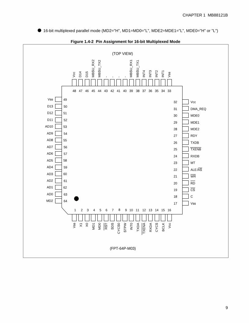
● 16-bit multiplexed parallel mode (MD2="H", MD1=MD0="L", MDE2=MDE1="L", MDE0="H" or "L")
Figure 1.4-2 Pin Assignment for 16-bit Multiplexed Mode
49
50
51
52
53
54
55
56
57
58
59
60
61
62
63
64
1
2
3
4
5
6
7
8
9
10
11
12
13
14
15
16
Vss 17
C 18
CS 19
RD 20
WR 21
ALE/AS 22
MT 23
RXDB 24
TXENB 25
TXDB 26
RDY 27
MDE2 28
MDE1 29
MDE0 30
DMA_REQ 31
Vcc 32
33
34
35
36
37 38 39 40 41 42 43 44 45 46
47
48
(TOP VIEW)
(FPT-64P-M03)
Vss X1
X0
MD
1
MD
0
RS
T
SD
S
CY
CS
0
ST
PW
INT
0
TX
DA
TX
EN
A
RX
DA
CY
CS
BC
LK
Vcc
Vss
D13
D12
D11
AD10
AD9
AD8
AD7
AD6
AD5
AD4
AD3
AD2
AD1
AD0
MD2
Vss
INT
1
INT
2
INT
3
D1
5
D1
4
Vcc
INT
4
MB
SU
_T
X1
MB
SU
_R
X1
MB
SU
_T
X2
MB
SU
_R
X2
- - - -
9

CHAPTER 1 MB88121B
● SPI mode (MD2=MD1="H", MD0="L", MDE2="H" or "L", MDE1="H" or "L", MDE0="L")
Figure 1.4-3 Pin Assignment for SPI Mode
49
50
51
52
53
54
55
56
57
58
59
60
61
62
63
64
1
2
3
4
5
6
7
8
9
10
11
12
13
14 15
16
Vss 17
C 18
CS 19
20
21
22
MT 23
RXDB 24
TXENB 25
TXDB 26
27
MDE2 28
MDE1 29
MDE0 30
31
Vcc 32
33
Vss
34
INT
1
35 36 37 38 39 40 41 42 43 44 45 46 47 48
Vcc
(TOP VIEW)
(FPT-64P-M03)
SC
K
MB
SU
_T
X1
MB
SU
_R
X1
MB
SU
_T
X2
MB
SU
_R
X2
SD
I
SD
O
Vss
MDS2
MDS1
MDS0
INT2
INT3
INT4
MD2
Vss X1
X0
MD
1
MD
0
RS
T
SD
S
CY
CS
0
ST
PW
INT
0
TX
DA
TX
EN
A
RX
DA
CY
CS
Vcc
- - - - - -
-
-
-
-
-
-
-
-
-
-
-
-
-
-
10

CHAPTER 1 MB88121B
1.5 Pin Functions
This section explains the pin functions of the MB88121B.
■ Pin Functions
Table 1.5-1 Pin Functions (1 / 7)
Pin No. Pin Name Circuit Type Function Description
1, 17, 33, 49 Vss - GND pins
16, 32, 48 Vcc -5V or 3.3V power supply pins. Connect all of the power supply pins to the same potential.
18 C -Power supply stabilization capacitor pin. Connect to a ceramic capacitor with a capacitance of 0.1 µF or more.
2 X1C
Oscillator pin
3 X0 Oscillator pin. Also used as the external clock input pin.
64, 4, 5 MD2 to MD0 B
Operation mode selection inputs.
See "2.4 FlexRay Operations" for details.Note:
Operation is not guaranteed if settings other than those listed above are used.
6 RST A
External reset input. The device is initialized when this pin is set to "L".Note:
Always set this pin to "L" when the power supply is connected, and maintain the "L" until the oscillation stabilization wait time has elapsed.
7 SDS B
Indicates the start of a dynamic segment. A dynamic segment is started and an "H" pulse is output when the SDSE bit of the Debug Support Register (DBGS) is set to "1". This pin is fixed at "L" when the SDSE bit of the Debug Support Register is set to "0".
8 CYCS0 B
Indicates the start of cycle 0. Cycle 0 is started and an "H" pulse is output when the CYCS0E bit of the Debug Support Register (DBGS) is set to "1". This pin is fixed at "L" when the CYCS0E bit of the Debug Support Register is set to "0".Note:
Cycle 0 does not output an "H" pulse on release from reset.
9 STPW BStop watch trigger input. Functions as the stop watch trigger as specified by the setting of Stop Watch Register 1 (STPW1).
MD2 MD1 MD0 Mode
1 0 0 16-bit parallel bus
1 1 0 Serial bus
11

CHAPTER 1 MB88121B
10 INT0 BInterrupt 0 output. This pin changes to "H" to indicate the occurrence of an interrupt. This interrupt is enabled and disabled using the EINT0 bit of the Interrupt Line Enable Register (ILE).
11 TXDA B Data output for ch.A.
12 TXENA BOperation enable output for ch.A. Transmit data output is enabled when this pin is "L". This pin is set to "H" on reset.
13 RXDA B Data input for ch.A.
14 CYCS BIndicates the start of cycle. Cycle is started and "H" pulse is output when the CYCSE bit of the debug support register (DBGS) is set to "1". This pin is fixed at "L" when the CYCSE bit of the debug support register is set to "0".
15
BCLK
B
Bus clock input.
-In SPI mode, this pin is set to high impedance state. Use the device with this pin left open or fixed at "L".
19 CS B Chip select input. The chip is selected when this pin is "L".
20
RD
B
Read enable input. The register value is output to pins D15 to D0 when CS="L" and this pin is "L". Do not set WR="L" when RD="L".
-In SPI mode, this pin is set to high impedance state.Use the device with this pin left open, or fixed at "H" or "L".
21
WR
B
Write enable input. The data on pins D15 to D0 is written to the register when CS="L" and this pin is "L". Do not set RD="L" when WR="L".
-In SPI mode, this pin is set to high impedance state.Use the device with this pin left open, or fixed at "H" or "L".
22
INT2
B
In the 16-bit non-multiplexed bus mode, this pin is the interrupt output of Timer 0 or Timer 1. This pin changes to "H" to indicate the occurrence of Interrupt 2 or Interrupt 3. A Timer 0 or Timer 1 interrupt occurs when the TINTE0 bit or the TINTE1 bit of the Interrupt Register (INT) is set to "1".Note:
The output state of this pin is undefined when the power is turned on.
AS
In FR460 mode of the 16-bit multiplexed bus mode, this pin is the address strobe input. This signal is active low.Note:
The output state of this pin is undefined when the power is turned on.
ALE
In 16FX mode of the 16-bit multiplexed bus mode, this pin is the address latch enable input. This pin is active high.Note:
The output state of this pin is undefined when the power is turned on.
-
In SPI mode, this pin is set to high impedance state.Use the device with this pin left open, or fixed at "H" or "L".Note:
The output state of this pin is undefined when the power is turned on.
Table 1.5-1 Pin Functions (2 / 7)
Pin No. Pin Name Circuit Type Function Description
12

CHAPTER 1 MB88121B
23 MT B
Indicates the start of a macrotick. A macrotick is started and an "H" pulse is output when the MTE bit of the Debug Support Register (DBGS) is set to "1". This pin is fixed at "L" when the MTE bit of the Debug Support Register is set to "0".
24 RXDB B Data input for ch.B.
25 TXENB BOperation enable output for ch.B. Transmit data output is enabled when this pin is "L". This pin is set to "H" on reset.
26 TXDB B Data output for ch.B.
27
RDY
B
Ready output. The device is in the ready state when this pin is "H".
-In SPI mode, this pin is set to high impedance state.Use the device with this pin left open, or fixed at "H" or "L".
28 to 30MDE2 to
MDE0B Extended mode selection inputs.
31
DMA_REQ
B
DMA TRANSFER REQUEST OUTPUT. SET TO HIGH IMPEDANCE STATE ON RESET. This output is enabled by the DMAOE bit of the DMA Support Register (DMAS).
-In SPI mode, this pin is set to high impedance state.Use the device with this pin left open, or fixed at "H" or "L".
34 INT1 BINTERRUPT 1 OUTPUT. THIS PIN CHANGES TO "H" TO INDICATE THE OCCURRENCE OF AN INTERRUPT. This interrupt is enabled and disabled using the EINT1 bit of the Interrupt Line Enable Register (ILE).
35
A10
B
In the 16-bit non-multiplexed bus mode, this pin is an address input.Note:
The output state of this pin is undefined when the power is turned on.
INT2
IN THE 16-BIT MULTIPLEXED BUS MODE, THIS PIN IS THE INTERRUPT 2 OUTPUT. This pin changes to "H" to indicate the occurrence of an interrupt. If the TINTE0 bit of the Interrupt Register (INT) is set to "1", "H" is output when a Timer 0 interrupt occurs. If the TINTE0 bit of the Interrupt Register (INT) is set to "0", this output is fixed at "L".Note:
The output state of this pin is undefined when the power is turned on.
-
In SPI mode, this pin is set to high impedance state.Use the device with this pin left open, or fixed at "H" or "L".Note:
The output state of this pin is undefined when the power is turned on.
Table 1.5-1 Pin Functions (3 / 7)
Pin No. Pin Name Circuit Type Function Description
13

CHAPTER 1 MB88121B
36
A9
B
In the 16-bit non-multiplexed bus mode, this pin is an address input.Note:
The output state of this pin is undefined when the power is turned on.
INT3
In the 16-bit multiplexed bus mode, this pin is the Interrupt 3 output. This pin changes to "H" to indicate the occurrence of an interrupt. If the TINTE1 bit of the Interrupt Register (INT) is set to "1", "H" is output when a Timer 1 interrupt occurs. If the TINTE1 bit of the Interrupt Register (INT) is set to "0", this output is fixed at "L".Note:
The output state of this pin is undefined when the power is turned on.
-
In SPI mode, this pin is set to high impedance state.Use the device with this pin left open, or fixed at "H" or "L".Note:
The output state of this pin is undefined when the power is turned on.
37
A8
B
In the 16-bit non-multiplexed bus mode, this pin is an address input.Note:
The output state of this pin is undefined when the power is turned on.
INT4
In the 16-bit multiplexed bus mode, this pin is the low-voltage detection interrupt output. This pin changes to "H" to indicate the occurrence of an interrupt. If the LVD5E bit or the LVD18E bit of the Interrupt Register (INT) is set to "1", this pin changes to "H" when the LVD5 bit or the LVD18 bit of the Interrupt Register (INT) changes to "1". If the LVD5E bit and the LVD18E bits of the Interrupt Register (INT) are set to "0", this output is fixed at "L".Note:
The output state of this pin is undefined when the power is turned on.
-
In SPI mode, this pin is set to high impedance state.Use the device with this pin left open, or fixed at "H" or "L".Note:
The output state of this pin is undefined when the power is turned on.
38
A7
B
In the 16-bit non-multiplexed bus mode, this pin is an address input.Note:
The output state of this pin is undefined when the power is turned on.
MBSU_TX1
In the 16-bit multiplexed bus mode and SPI mode, this pin indicates changes in the message buffer status of the ch.A transmit buffer. If the MBSUE bit of the Debug Support Register (DBGS) is set to "1", this pin changes to "H" when the message buffer is updated. If the MBSUE bit of the Debug Support Register (DBGS) is set to "0", this pin is fixed at "L".Note:
The output state of this pin is undefined when the power is turned on.
Table 1.5-1 Pin Functions (4 / 7)
Pin No. Pin Name Circuit Type Function Description
14
CHAPTER 1 MB88121B
39
A6
B
In the 16-bit non-multiplexed bus mode, this pin is an address input.Note:
The output state of this pin is undefined when the power is turned on.
MBSU_RX1
In the 16-bit multiplexed bus mode and SPI mode, this pin indicates changes in the message buffer status of the ch.A transmit buffer. If the MBSUE bit in the Debug Support Register (DBGS) is set to "1", this pin changes to "H" when the message buffer is updated. If the MBSUE bit of the Debug Support Register (DBGS) is set to "0", this pin is fixed at "L".Note:
The output state of this pin is undefined when the power is turned on.
40
A5
B
In the 16-bit non-multiplexed bus mode, this pin is an address input.
-In the 16-bit multiplexed bus mode, this pin is set to high impedance state.Use the device with this pin left open, or fixed at "H" or "L".
SCKIn SPI mode, this pin is the serial clock input. The operation mode is determined by the MDS1 and MDS0 settings.
41
A4
B
In the 16-bit non-multiplexed bus mode, this pin is an address input.
-In the 16-bit multiplexed bus mode, this pin is set to high impedance state.Use the device with this pin left open, or fixed at "H" or "L".
SDIIn SPI mode, this pin is the serial data input. Input serial data to this pin synchronously with the serial clock according to the operation mode.
42
A3
B
In the 16-bit non-multiplexed bus mode, this pin is an address input.
-In the 16-bit multiplexed bus mode, this pin is set to high impedance state.Use the device with this pin left open, or fixed at "H" or "L".
SDOIn SPI mode, this pin is the serial data output. When CS="L", serial data is output synchronously with the serial clock according to the operation mode.When CS="H", this pin is set to high impedance state.
43
A2
B
In the 16-bit non-multiplexed bus mode, this pin is an address input.
-In the 16-bit multiplexed bus mode and SPI mode, this pin is set to high impedance state.Use the device with this pin left open, or fixed at "H" or "L".
44
A1
B
In the 16-bit non-multiplexed bus mode, this pin is an address input.Note:
The output state of this pin is undefined when the power is turned on.
MBSU_TX2
In the 16-bit multiplexed bus mode, this pin indicates changes in the message buffer status of the ch.B transmit buffer. If the MBSUE bit in the Debug Support Register (DBGS) is set to "1", this pin changes to "H" when the message buffer is updated. If the MBSUE bit of the Debug Support Register (DBGS) is set to "0", this pin is fixed at "L".Note:
The output state of this pin is undefined when the power is turned on.
Table 1.5-1 Pin Functions (5 / 7)
Pin No. Pin Name Circuit Type Function Description
15
CHAPTER 1 MB88121B
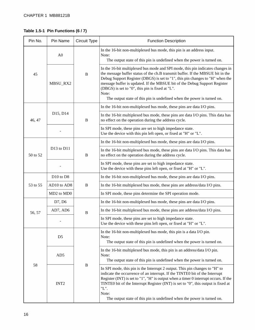
45
A0
B
In the 16-bit non-multiplexed bus mode, this pin is an address input.Note:
The output state of this pin is undefined when the power is turned on.
MBSU_RX2
In the 16-bit multiplexed bus mode and SPI mode, this pin indicates changes in the message buffer status of the ch.B transmit buffer. If the MBSUE bit in the Debug Support Register (DBGS) is set to "1", this pin changes to "H" when the message buffer is updated. If the MBSUE bit of the Debug Support Register (DBGS) is set to "0", this pin is fixed at "L".Note:
The output state of this pin is undefined when the power is turned on.
46, 47
D15, D14
B
In the 16-bit non-multiplexed bus mode, these pins are data I/O pins.
In the 16-bit multiplexed bus mode, these pins are data I/O pins. This data has no effect on the operation during the address cycle.
-In SPI mode, these pins are set to high impedance state.Use the device with this pin left open, or fixed at "H" or "L".
50 to 52
D13 to D11
B
In the 16-bit non-multiplexed bus mode, these pins are data I/O pins.
In the 16-bit multiplexed bus mode, these pins are data I/O pins. This data has no effect on the operation during the address cycle.
-In SPI mode, these pins are set to high impedance state.Use the device with these pins left open, or fixed at "H" or "L".
53 to 55
D10 to D8
B
In the 16-bit non-multiplexed bus mode, these pins are data I/O pins.
AD10 to AD8 In the 16-bit multiplexed bus mode, these pins are address/data I/O pins.
MD2 to MD0 In SPI mode, these pins determine the SPI operation mode.
56, 57
D7, D6
B
In the 16-bit non-multiplexed bus mode, these pins are data I/O pins.
AD7, AD6 In the 16-bit multiplexed bus mode, these pins are address/data I/O pins.
-In SPI mode, these pins are set to high impedance state.Use the device with these pins left open, or fixed at "H" or "L".
58
D5
B
In the 16-bit non-multiplexed bus mode, this pin is a data I/O pin.Note:
The output state of this pin is undefined when the power is turned on.
AD5In the 16-bit multiplexed bus mode, this pin is an address/data I/O pin.Note:
The output state of this pin is undefined when the power is turned on.
INT2
In SPI mode, this pin is the Interrupt 2 output. This pin changes to "H" to indicate the occurrence of an interrupt. If the TINTE0 bit of the Interrupt Register (INT) is set to "1", "H" is output when a timer 0 interrupt occurs. If the TINTE0 bit of the Interrupt Register (INT) is set to "0", this output is fixed at "L".Note:
The output state of this pin is undefined when the power is turned on.
Table 1.5-1 Pin Functions (6 / 7)
Pin No. Pin Name Circuit Type Function Description
16

CHAPTER 1 MB88121B
59
D4
B
In the 16-bit non-multiplexed bus mode, this pin is a data I/O pin.Note:
The output state of this pin is undefined when the power is turned on.
AD4In the 16-bit multiplexed bus mode, this pin is an address/data I/O pin.Note:
The output state of this pin is undefined when the power is turned on.
INT3
In SPI mode, this pin is the Interrupt 3 output. This pin changes to "H" to indicate the occurrence of an interrupt. If the TINTE1 bit of the Interrupt Register (INT) is set to "1", "H" is output when a timer 1 interrupt occurs. If the TINTE1 bit of the Interrupt Register (INT) is set to "0", this output is fixed at "L".Note:
The output state of this pin is undefined when the power is turned on.
60
D3
B
In the 16-bit non-multiplexed bus mode, this pin is a data I/O pin.Note:
The output state of this pin is undefined when the power is turned on.
AD3In the 16-bit multiplexed bus mode, this pin is an address/data I/O pin.Note:
The output state of this pin is undefined when the power is turned on.
INT4
In SPI mode, this pin is the low-voltage detection interrupt output. This pin changes to "H" to indicate the occurrence of an interrupt. If the LVD5E bit or the LVD18E bit of the Interrupt Register (INT) is set to "1" and the LVD5 bit or the LVD18 bit of the Interrupt Register (INT) is set to "1", this pin changes to "H". If the LVD5E bit and the LVD18E bit of the Interrupt Register (INT) are set to "0", this output is fixed at "L".Note:
The output state of this pin is undefined when the power is turned on.
61 to 63
D2 to D0
B
In the 16-bit non-multiplexed bus mode, these pins are data I/O pins.Note:
The output state of these pins is undefined when the power is turned on.
AD2 to AD0In the 16-bit multiplexed bus mode, these pins are address/data I/O pins.Note:
The output state of these pins is undefined when the power is turned on.
-In SPI mode, these pins are set to high impedance state.Use the device with these pins left open, or fixed at "H" or "L".
Table 1.5-1 Pin Functions (7 / 7)
Pin No. Pin Name Circuit Type Function Description
17

CHAPTER 1 MB88121B
1.6 I/O Circuit Types
I/O circuit types of MB88121B are shown below.
■ I/O Circuit Types
Table 1.6-1 I/O Circuit Types
Type Circuit
A
B
C
Input
Input
Input enable
Output drive N-ch
Output drive P-chP-ch
N-ch
Standby control
X1
X0
Hysteresis input
18
CHAPTER 1 MB88121B
1.7 Notes on Handling Devices
This section explains the notes when handling the devices.
■ Notes on Handling Devices
● When turning on the power supply
Always set the reset (RST) signal to "L" immediately after turning the power on in order to initialize the
device.
● Undefined outputs at power-on
When the power is turned on, the state of input/output pins remain undefined until the power supply
voltage reaches the recommended operating range.
● Preventing latch-up
Latch-up is a phenomenon that may occur if a voltage in excess of the maximum rated value is applied
between the Vss pins and the input pins, output pins, or Vcc pins. When latch-up occurs, the power supply
current increases dramatically and components may be burned out. Therefore, ensure that operating
voltages do not exceed the absolute maximum rated values when the device is being used.
● Power supply pins
This device has multiple Vcc pins and multiple Vss pins. Ensure that these pins are all connected to the 5V
power supply or to ground. Furthermore, use low impedance connections between the power supply source
and the Vcc pins and Vss pins on the device to ensure that voltage differences do not occur.
● Handling unused pins
If unused input pins are left unconnected, malfunctions may occur and the device may be permanently
damaged due to latch-up.
Handle unused input and input/output pins by connecting them to a pull-up or pull-down resistance of 2 k
or more.
Leave unused output pins unconnected.
● Mode pins (MD0, MD1, MD2, MDE0, MDE1, MDE2)
Connect the mode pins directly to Vcc or Vss to prevent the device from entering the wrong mode due to
noise on these pins. In addition, keep the length of the pattern on the printed circuit board between the
mode pins and the Vcc or Vss pins as short as possible.
19
CHAPTER 1 MB88121B
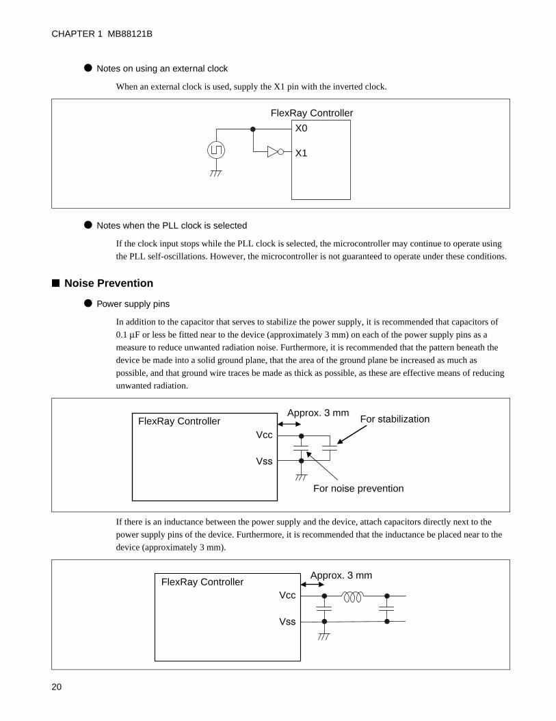
● Notes on using an external clock
When an external clock is used, supply the X1 pin with the inverted clock.
● Notes when the PLL clock is selected
If the clock input stops while the PLL clock is selected, the microcontroller may continue to operate using
the PLL self-oscillations. However, the microcontroller is not guaranteed to operate under these conditions.
■ Noise Prevention
● Power supply pins
In addition to the capacitor that serves to stabilize the power supply, it is recommended that capacitors of
0.1 µF or less be fitted near to the device (approximately 3 mm) on each of the power supply pins as a
measure to reduce unwanted radiation noise. Furthermore, it is recommended that the pattern beneath the
device be made into a solid ground plane, that the area of the ground plane be increased as much as
possible, and that ground wire traces be made as thick as possible, as these are effective means of reducing
unwanted radiation.
If there is an inductance between the power supply and the device, attach capacitors directly next to the
power supply pins of the device. Furthermore, it is recommended that the inductance be placed near to the
device (approximately 3 mm).
X0 X1
FlexRay Controller
FlexRay Controller Vcc
Vss
For stabilization
For noise prevention
Approx. 3 mm
FlexRay ControllerVcc
Vss
Approx. 3 mm
20
CHAPTER 1 MB88121B
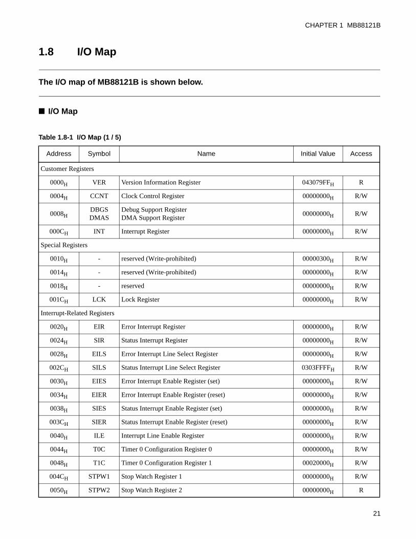
1.8 I/O Map
The I/O map of MB88121B is shown below.
■ I/O Map
Table 1.8-1 I/O Map (1 / 5)
Address Symbol Name Initial Value Access
Customer Registers
0000H VER Version Information Register 043079FFH R
0004H CCNT Clock Control Register 00000000H R/W
0008HDBGSDMAS
Debug Support RegisterDMA Support Register
00000000H R/W
000CH INT Interrupt Register 00000000H R/W
Special Registers
0010H - reserved (Write-prohibited) 00000300H R/W
0014H - reserved (Write-prohibited) 00000000H R/W
0018H - reserved 00000000H R/W
001CH LCK Lock Register 00000000H R/W
Interrupt-Related Registers
0020H EIR Error Interrupt Register 00000000H R/W
0024H SIR Status Interrupt Register 00000000H R/W
0028H EILS Error Interrupt Line Select Register 00000000H R/W
002CH SILS Status Interrupt Line Select Register 0303FFFFH R/W
0030H EIES Error Interrupt Enable Register (set) 00000000H R/W
0034H EIER Error Interrupt Enable Register (reset) 00000000H R/W
0038H SIES Status Interrupt Enable Register (set) 00000000H R/W
003CH SIER Status Interrupt Enable Register (reset) 00000000H R/W
0040H ILE Interrupt Line Enable Register 00000000H R/W
0044H T0C Timer 0 Configuration Register 0 00000000H R/W
0048H T1C Timer 0 Configuration Register 1 00020000H R/W
004CH STPW1 Stop Watch Register 1 00000000H R/W
0050H STPW2 Stop Watch Register 2 00000000H R
21

CHAPTER 1 MB88121B
0054Hto
007CH
- reserved 00000000H R
Communication Controller (CC) Control Registers
0080H SUCC1 SUC Configuration Register 1 0C401000H R/W
0084H SUCC2 SUC Configuration Register 2 01000504H R/W
0088H SUCC3 SUC Configuration Register 3 00000003H R/W
008CH NEMC NEM Configuration Register 00000000H R/W
0090H PRTC1 PRT Configuration Register 1 084C0633H R/W
0094H PRTC2 PRT Configuration Register 2 0F2D0A0EH R/W
0098H MHDC MHD Configuration Register 00000000H R/W
009CH - reserved 00000000H R
00A0H GTUC1 GTU Configuration Register 1 00000280H R/W
00A4H GTUC2 GTU Configuration Register 2 0002000AH R/W
00A8H GTUC3 GTU Configuration Register 3 02020000H R/W
00ACH GTUC4 GTU Configuration Register 4 00080007H R/W
00B0H GTUC5 GTU Configuration Register 5 0E000000H R/W
00B4H GTUC6 GTU Configuration Register 6 00020000H R/W
00B8H GTUC7 GTU Configuration Register 7 00020004H R/W
00BCH GTUC8 GTU Configuration Register 8 00000002H R/W
00C0H GTUC9 GTU Configuration Register 9 00000101H R/W
00C4H GTUC10 GTU Configuration Register 10 00020005H R/W
00C8H GTUC11 GTU Configuration Register 11 00000000H R/W
00CCHto
00FCH
- reserved 00000000H R
Communication Controller (CC) Status Registers
0100H CCSV CC Status Vector Register 00104000H R
0104H CCEV CC Error Vector Register 00000000H R
0108Hto
010CH
- reserved 00000000H R
0110H SCV Slot Counter Value Register 00000000H R
Table 1.8-1 I/O Map (2 / 5)
Address Symbol Name Initial Value Access
22

CHAPTER 1 MB88121B
0114H MTCCV Macrotick and Cycle Counter Value Register 00000000H R
0118H RCV Rate Correction Value Register 00000000H R
011CH OCV Offset Correction Value Register 00000000H R
0120H SFS Sync Frame Status Register 00000000H R
0124H SWNIT Symbol Window and NIT Status Register 00000000H R
0128H ACS Aggregated Channel Status Register 00000000H R/W
012CH - reserved 00000000H R
0130Hto
0168H
ESIDn Even Cycle Sync Frame ID Register 00000000H R
016CH - reserved 00000000H R
0170Hto
01A8H
OSIDn Odd numbered Cycle Sync Frame ID Register 00000000H R
01ACH - reserved 00000000H R
01B0Hto
01B8H
NMVn Network Management Registers 1 to 3 00000000H R
01BCH to 02FCH
- reserved 00000000H R
Message Buffer Control Registers
0300H MRC Message RAM Configuration Register 01800000H R/W
0304H FRF FIFO Rejection Filter Register 01800000H R/W
0308H FRFM FIFO Rejection Filter Mask Register 00000000H R/W
030CH FCL FIFO Critical Level Register 00000080H R/W
Message Buffer Status Registers
0310H MHDS Message Handler Status Register 00000000H R/W
0314H LDTS Last Dynamic Transmit Slot Register 00000000H R
0318H FSR FIFO Status Register 00000000H R
031CH MHDF Message Handler Constraints Flags Register 00000000H R/W
0320H TXRQ1 Transmission Request Register 1 00000000H R
0324H TXRQ2 Transmission Request Register 2 00000000H R
0328H TXRQ3 Transmission Request Register 3 00000000H R
032CH TXRQ4 Transmission Request Register 4 00000000H R
Table 1.8-1 I/O Map (3 / 5)
Address Symbol Name Initial Value Access
23

CHAPTER 1 MB88121B
0330H NDAT1 New Data Register 1 00000000H R
0334H NDAT2 New Data Register 2 00000000H R
0338H NDAT3 New Data Register 3 00000000H R
033CH NDAT4 New Data Register 4 00000000H R
0340H MBSC1 Message Buffer Status Changed Register 1 00000000H R
0344H MBSC2 Message Buffer Status Changed Register 2 00000000H R
0348H MBSC3 Message Buffer Status Changed Register 3 00000000H R
034CH MBSC4 Message Buffer Status Changed Register 4 00000000H R
0350Hto
03ECH
- reserved 00000000H R
Identification Registers
03F0H CREL Core Release Register 07260412H R
03F4H ENDN Endian Register 87654321H R
03F8Hto
03FCH
- reserved 00000000H R
Input Buffers
0400Hto
04FCH
WRDSn Write Data Section Registers 1 to 64 00000000H R/W
0500H WRHS1 Write Header Section Register 1 00000000H R/W
0504H WRHS2 Write Header Section Register 2 00000000H R/W
0508H WRHS3 Write Header Section Register 3 00000000H R/W
050CH - reserved 00000000H R/W
0510H IBCM Input Buffer Command Mask Register 00000000H R/W
0514H IBCR Input Buffer Command Request Register 00000000H R/W
0518Hto
05FCH
- reserved 00000000H R
Output Buffers
0600Hto
06FCH
RDDSn Read Data Section Registers 1 to 64 00000000H R
0700H RDHS1 Read Header Section Register 1 00000000H R
Table 1.8-1 I/O Map (4 / 5)
Address Symbol Name Initial Value Access
24
CHAPTER 1 MB88121B
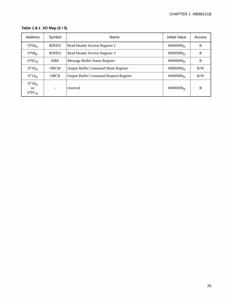
0704H RDHS2 Read Header Section Register 2 00000000H R
0708H RDHS3 Read Header Section Register 3 00000000H R
070CH MBS Message Buffer Status Register 00000000H R
0710H OBCM Output Buffer Command Mask Register 00000000H R/W
0714H OBCR Output Buffer Command Request Register 00000000H R/W
0718Hto
07FCH
- reserved 00000000H R
Table 1.8-1 I/O Map (5 / 5)
Address Symbol Name Initial Value Access
25

CHAPTER 1 MB88121B
26

CHAPTER 2FlexRay
This chapter explains the functions and operations of FlexRay.
2.1 Overview of FlexRay
2.2 Block Diagram of FlexRay
2.3 Configuration of FlexRay
2.4 FlexRay Operations
2.5 SPI Protocol Definition
2.6 FlexRay Controller Clock
2.7 FlexRay Protocol Function
27

CHAPTER 2 FlexRay
2.1 Overview of FlexRay
This section explains the overview of FlexRay.
■ Overview of FlexRayThe FlexRay controller performs communications compliant with the FlexRay Protocol Specifications
Version 2.1. When the maximum sample clock is specified, the bit rate is set to 10 Mbps.
The length of the message buffers for FlexRay network communications is configurable up to a maximum
of 254 data bytes. The message storage region consists of single-port message RAM that holds up to 128
message buffers. The message handler provides the following functions related to all aspects of message
processing.
• Acceptance filtering
• Message transfers between the two FlexRay channel protocol controllers and message RAM
• Transfer schedule management
• Providing message status information
The FlexRay controller registers can be accessed by the host. These registers are used to configure, control,
and monitor the following.
• FlexRay channel protocol controllers
• Message handler
• Global time unit
• System universal control
• Frame and symbol processing
• Network management
• Interrupt control
• Accessing message RAM via input/output buffers
28

CHAPTER 2 FlexRay
■ FlexRay FeaturesThe FlexRay controller supports the following functions.
• Complies with FlexRay Protocol Specification Version 2.1
• Each channel has a maximum bitrate of 10 Mbps
• Up to a maximum of 128 message buffers can be configured
• 8 Kbytes of message RAM
- 128 message buffers when the data section is 48 bytes
- 30 message buffers when the data section is 254 bytes
• Variable length message buffer configuration
• Configurable receive FIFO
• Each message buffer may be configured as a transmit buffer, receive buffer, or part of the receive FIFO
• Host access to message buffers via an input buffer and an output buffer
- Input buffer: Stores a message to be transferred to the message RAM
- Output buffer: Stores a message that has been read out from the message RAM
• Filtering by slot counter, cycle counter, and channel
• Maskable interrupts
• Network management support
29
CHAPTER 2 FlexRay
2.2 Block Diagram of FlexRay
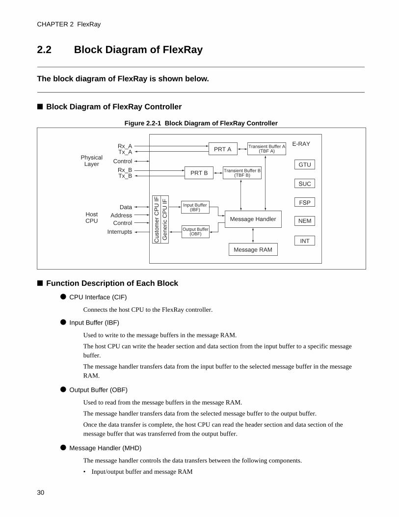
The block diagram of FlexRay is shown below.
■ Block Diagram of FlexRay Controller
Figure 2.2-1 Block Diagram of FlexRay Controller
■ Function Description of Each Block
● CPU Interface (CIF)
Connects the host CPU to the FlexRay controller.
● Input Buffer (IBF)
Used to write to the message buffers in the message RAM.
The host CPU can write the header section and data section from the input buffer to a specific message
buffer.
The message handler transfers data from the input buffer to the selected message buffer in the message
RAM.
● Output Buffer (OBF)
Used to read from the message buffers in the message RAM.
The message handler transfers data from the selected message buffer to the output buffer.
Once the data transfer is complete, the host CPU can read the header section and data section of the
message buffer that was transferred from the output buffer.
● Message Handler (MHD)
The message handler controls the data transfers between the following components.
• Input/output buffer and message RAM
Message Handler
Message RAM
E-RAY
Output Buffer(OBF)
Cus
tom
er C
PU
IFG
ener
ic C
PU
IF Input Buffer(IBF)
Interrupts
Control
ControlPhysical
Layer
HostCPU
AddressData
Rx_BTx_B
Rx_ATx_A
PRT B Transient Buffer B(TBF B)
Transient Buffer A(TBF A)
GTU
SUC
FSP
NEM
INT
PRT A
30
CHAPTER 2 FlexRay
• The transient storage buffer RAM of the two FlexRay protocol controllers and message RAM
● Message RAM (MRAM)
The message RAM is composed of single-port RAM that is able to hold the configuration data for the built-
in FlexRay message buffers (max. 128).
■ Transient Buffer RAM (TBF A/B)Stores the data sections of two messages.
■ FlexRay Channel Protocol Controller (PRT A/B)The FlexRay channel protocol controller is composed of a shift register and a FlexRay protocol FSM.
The protocol controller provides the following functions.
• Checking and controlling bit timings
• Receiving and transmitting FlexRay frames and symbols
• Checking the header CRC
• Generating and checking frame CRC
• Connecting to the bus driver
In addition, protocol controller block is connected to the following blocks.
• Physical layer (bus driver)
• Transient storage buffer RAM
• Message handler
• Global time unit
• System universal control
• Frame and symbol processing
• Network management
• Interrupt control
■ Global Time Unit (GTU)• The global time unit provides the following functions.
• Generating microticks
• Generating macroticks
• Fault-tolerant clock synchronization using the FTM algorithm
- Rate correction
- Offset correction
• Cycle counter
• Static segment timing control
• Dynamic segment (minislot) timing control
• Support for external clock correction
31

CHAPTER 2 FlexRay
■ System Universal Control (SUC)
The system universal control controls the following functions.
• Configuration
• Wakeup
• Startup
• Normal operation
• Passive operation
• Monitor mode
■ Frame and Symbol Processing (FSP)Frame and symbol processing controls the following function.
• Checking that the timing of frames and symbols is correct
• Testing the syntactic and semantic validity of received frames
• Setting the slot status flag
■ Network Management (NEM)Configures the handling of the network management vector.
■ Interrupt Control (INT)The following functions are available for controlling interrupts.
• Provision of error and interrupt flags
• Controlling the enabling/disabling of interrupt sources
• Controlling the allocation of interrupt sources to the two interrupt lines of the module
• Enabling/disabling the two interrupt lines of the module
• Managing the two interrupt timers
• Halting watch timer capturing
32
CHAPTER 2 FlexRay
2.3 Configuration of FlexRay
This section explains the configuration of FlexRay.
■ Configuration of FlexRayThe FlexRay controller has an address space of 2 Kbytes (0000H to 07FFH) that is composed of 32-bit
registers. Host access to the message RAM (access by the host CPU) is performed via the input buffer and
output buffer. In order to prevent competition between host access and the reception and transmission of
messages, these buffers are used to buffer data for transfer to the message RAM and data that has been
transferred from the message RAM.
The number N of message buffers that can be used depends on the configured message buffer payload
length. The maximum number of message buffers is 128 and the maximum payload length is 254 bytes.
The message buffers are allocated as shown in Figure 2.3-1. The message buffers are organized into three
consecutive groups.
• Static buffers: Transmit and receive buffers allocated to static segments
• Static + dynamic buffers: Transmit and receive buffers allocated to static segments or dynamic segments
• FIFO: Receive FIFO
The allocation of message buffers can be changed by setting the Message RAM Configuration Register
(MRC) while in the DEFAULT_CONFIG or CONFIG states.
The first group operates as static message buffers.
The second group operates as static/dynamic message buffers. The message buffers that belong to this group
can be reconfigured during operation from dynamic segments to static segments, or from static segments to
dynamic segments depending on the state of MRC:SEC1 and SEC0.
Message buffers that belong to the third group are connected into receive FIFO.
Message buffer 0 is used to store and transmit startup, synchronization, or single slot frames (a frame that is
sent in the single slot mode) depending on the setting of SUCC1:TXST, TXSY, and TSM. Message buffer
0 is required to have a key slot ID, which can only be configured (or reconfigured) in the
DEFAULT_CONFIG or CONFIG states.
33

CHAPTER 2 FlexRay
Figure 2.3-1 Allocation of Message Buffers
Note:
All of the FlexRay controller registers are accessed as 32 bits.
Message Buffer 0
Message Buffer 1
Message Buffer N
Message Buffer N-1
Static Buffers
Static + DynamicBuffers...
FDB: First Dynamic Buffer Number
FFB: First FIFO Buffer Number
LCB: Last Message Buffer Number
FIFO
34

CHAPTER 2 FlexRay
2.3.1 Customer Registers
This section explains the bit configurations and functions of the customer registers.
■ Customer RegistersThe address space from 0000H to 000FH is for MB88121B customer registers. These are allocated to
version information, clock control, debugging support, DMA support, and interrupt registers.
■ Version Information Register (VER)
Figure 2.3-2 Version Information Register Details
Address bit31 bit23bit24 bit15bit16 bit7bit8
bit31 to bit24
bit0
ECR7 to ECR0CIV7 to CIV0INV7 to INV0VID7 to VID0
RRRR
Initial Value
043079FFH0000H
R : Read only
VID7 to VID0 JEDEC ID Code
bit23 to bit16
INV7 to INV0 Revision Number Bits
bit15 to bit8
CIV7 to CIV0 LSI Identification Number Bits
bit7 to bit0
ECR7 to ECR0 FlexRay IP Identification Bits
35

CHAPTER 2 FlexRay
Table 2.3-1 Explanation of the Function of Each Bit in the Version Information Register
No. Bit Name Function
bit 31 to bit 24VID7 to VID0:JEDEC ID Code
Specifies the Fujitsu JEDEC ID code. On the MB88121B, reading these bits returns 04H. Writing to these bits has no effect on the operation.
bit 23 to bit 16INV7 to INV0:Revision Number Bits
Represents the revision number of the LSI. On the MB88121B, reading these bits returns 30H. Writing to these bits has no effect on the operation.
bit 15 to bit 8CIV7 to CIV0:LSI Identification Number Bits
Represents the identification number of the LSI. This is the lowest 3 digits of the MB number in hexadecimal notation.On the MB88121B, reading these bits returns 79H. Writing to these bits has no effect on the operation.
bit 7 to bit 0ECR7 to ECR0:FlexRay IP Identification Bits
Represents the FlexRay IP identification number. On the MB88121B, reading these bits returns FFH. If these bits return FFH, the IP information is stored in the CREL register. The CREL register there needs to be read as necessary. Writing to these bits has no effect on the operation.
36
CHAPTER 2 FlexRay
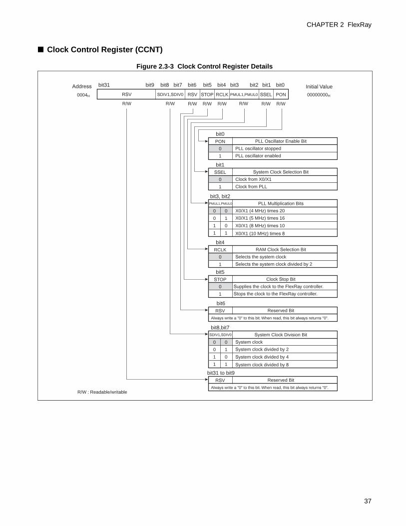
■ Clock Control Register (CCNT)
Figure 2.3-3 Clock Control Register Details
Address bit4bit5bit6bit7bit8bit9bit31 bit3 bit2 bit0
bit0
bit1 Initial Value
STOP RCLK SSEL PON 00000000HRSV
PON
0
1
SDIV1,SDIV0 PMUL1,PMUL0RSV
R/W R/W R/W R/WR/WR/W R/WR/W
0004H
R/W : Readable/writable
PLL Oscillator Enable Bit
PLL oscillator stopped
PLL oscillator enabled
bit1SSEL
0
1
System Clock Selection Bit
Clock from X0/X1
Clock from PLL
bit3, bit2PMUL1,PMUL0
0
0
1
1
0
1
0
1
PLL Multiplication Bits
X0/X1 (4 MHz) times 20
X0/X1 (5 MHz) times 16
X0/X1 (8 MHz) times 10
X0/X1 (10 MHz) times 8
bit4RCLK
0
1
RAM Clock Selection Bit
Selects the system clock
Selects the system clock divided by 2
bit5STOP
0
1
Clock Stop Bit
Supplies the clock to the FlexRay controller.
Stops the clock to the FlexRay controller.
bit31 to bit9RSV Reserved Bit
Always write a "0" to this bit. When read, this bit always returns "0".
bit6RSV Reserved Bit
Always write a "0" to this bit. When read, this bit always returns "0".
bit8,bit7SDIV1,SDIV0
0
0
1
1
0
1
0
1
System Clock Division Bit
System clock
System clock divided by 2
System clock divided by 4
System clock divided by 8
37

CHAPTER 2 FlexRay
Table 2.3-2 Explanation of the Function of Each Bit in the Clock Control Register (1 / 2)
No. Bit Name Function
bit 31 to bit 9RSV:Reserved bits
These bits are reserved. These bits always return "0" when read. Always write "0" to these bits.
bit 8, bit 7SDIV1, SDIV0:System ClockDivision Bits
Configures a frequency divider on the system clock (sclk*). The clock division
from these bits is used as the FlexRay operating clock (f_sclk*).
bit 6RSV:Reserved bit
This bit is reserved. This bit always returns "0" when read. Always write "0" to this bit.
bit 5STOP:Clock Stop Bit
Stops the system clock (sclk*). When this bit is set to "1", the system clock stops, but the oscillator circuit operates.Use the following procedures to set this bit to "1".
- When using the PLL
1) Prohibit the FlexRay controller from transmitting and receiving.2) Set the SSEL bit to "0"3) Set the PON bit to "0"4) Set the STOP bit to "1"
- When not using the PLL
1) Prohibit the FlexRay controller from transmitting and receiving.2) Set the STOP bit to "1"
Use the following procedures to set this bit to "0".
- When using the PLL
1) Set the PON bit to "1"2) Set the STOP bit to "0"3) After the PLL lock-up time (600 µs) has elapsed, set the SSEL bit to
"1"4) Enable the FlexRay controller to transmit and receive.
- When not using the PLL
Set the STOP bit to "0"
bit 4RCLK:RAM Clock Selection Bit
This bit selects whether the system clock (sclk*) is divided by two and used as
the RAM clock (f_bclk*) or used directly as the RAM clock.
SDIV1 SDIV0 Function
0 0 System clock
0 1 System clock divided by 2
1 0 System clock divided by 4
1 1 System clock divided by 8
38

CHAPTER 2 FlexRay
*: See "2.6 FlexRay Controller Clock".
Note:
The Clock Control Register can only be updated when the CCSV:POCS5 to POCS0 bits are in the DEFAULT_CONFIG state or the CONFIG state.
When the mode pins are set to the SPI mode setting (MDE0 = 0), the initial values of the CCNT:PMUL1 and PMUL0 bits at power-on or reset reflect the settings of the external input frequency pins (MDE2 and MDE1). Furthermore, the SPI mode setting sets the CCNT:PON bit to "1".
bit 3, bit 2PMUL1, PMUL0:PLL Multiplication Bits
Determines the PLL multiplication factor. Set these bits such that the PLL clock becomes 80 MHz.In SPI mode, the configuration values of the MDE2 and MDE1 pins are loaded into these bits upon release from reset.
Note:Change these bits before setting the PON bit to "1".
bit 1SSEL:
System Clock (sclk*) Selection Bit
This bit selects between the X0/X1 clock and the clock output from the PLL."0": Selects the clock from X0/X1."1": Selects the clock output from the PLL.
Notes:• When changing this bit from "0" to "1", first set the PON bit to "1" and then
ensure the PLL lock-up time (600 µs) before changing this bit.
• To stop the PLL oscillator, first set this bit to "0" before setting the PON bit to "0".
bit 0PON:PLL Oscillator Enable Bit
This bit enables the PLL oscillator.In SPI mode, this bit is set to "1" upon release from reset.
"0": Disables the PLL oscillator."1": Enables the PLL oscillator.
Note:Change this bit when the SSEL bit is "0".
Table 2.3-2 Explanation of the Function of Each Bit in the Clock Control Register (2 / 2)
No. Bit Name Function
PMUL1 PMUL0 Function
0 0 Multiply X0/X1 (4 MHz) by 20
0 1 Multiply X0/X1 (5 MHz) by 16
1 0 Multiply X0/X1 (8 MHz) by 10
1 1 Multiply X0/X1 (10 MHz) by 8
39

CHAPTER 2 FlexRay
■ Debug Support Register (DBGS)
Figure 2.3-4 Debug Support Register Details
Table 2.3-3 Explanation of the Function of Each Bit in the Debug Support Register (1 / 2)
No. Bit Name Function
bit 31MBSUE:MBSU Output Enable Bit
This bit enables the internal MBSU_TX1, MBSU_RX1, MBSU_TX2, and MBSU_RX2 signals to be output on the MBSU_TX1, MBSU_RX1, MBSU_TX2, and MBSU_RX2 pins. When this bit is set to "1", the internal signals are output, and when set to "0", the pins are fixed at "L".Note:
This setting is only active in SPI mode and multiplexed mode.
bit 30CYCSE:CYCS Output Enable Bit
This bit enables the internal CYCS signal (cycle start) to be output on the CYCS pin. When this bit is set to "1", the internal CYCS signal is output, and when set to "0", the CYCS pin is fixed at "L".
Address bit31 bit30 bit29 bit28 bit27 bit26 bit16 bit15 bit0 Initial ValueDMA Support (DMAS) 0000HRSVCYCS0EMTECYCSEMBSUE SDSE0008H
R/W R/WR/WR/W R/W R/W R/W
R/W : Readable/writable
bit26 to bit16RSV Reserved Bits
Always write "0" to these bits. When read, these bits always return "0".
bit27CYCS0E
0
1
CYCS0 Output Enable Bit
Output disabled
Output enabled
bit28SDSE
0
1
SDS Output Enable Bit
Output disabled
Output enabled
bit29MTE
0
1
MT Output Enable Bit
Output disabled
Output enabled
bit30CYCSE
0
1
CYCS Output Enable Bit
Output disabled
Output enabled
bit31MBSUE
0
1
MBSU Output Enable Bit
Output disabled
Output enabled
40

CHAPTER 2 FlexRay
■ DMA Support Register (DMAS)
Figure 2.3-5 DMA Support Register Details
bit 29MTE:MT Output Enable Bit
This bit enables the internal MT signal (macrotick) to be output on the MT pin. When this bit is set to "1", the internal MT signal is output, and when set to "0", the MT pin is fixed at "L".
bit 28SDSE:SDS Output Enable Bit
This bit enables the internal SDS signal (dynamic segment start) to be output on the SDS pin. When this bit is set to "1", the internal SDS signal is output, and when set to "0", the SDS pin is fixed at "L".
bit 27CYCS0E:CYCS0 Output EnableBit
This bit enables the internal CYCS0 signal (cycle 0 start) to be output on the CYCS0 pin. When this bit is set to "1", the internal CYCS0 signal is output, and when set to "0", the CYCS0 pin is fixed at "L".
bit 26 to bit 16 RSV: Reserved bitsThese bits are reserved. These bits always return "0" when read. Always write "0" to these bits.
Table 2.3-3 Explanation of the Function of Each Bit in the Debug Support Register (2 / 2)
No. Bit Name Function
Address bit31 bit16 bit15 bit3 bit1bit2 bit0 Initial Value
Debug Support (DBGS) 0000HRSV DMAINV DMARE DMAOE0008H
R/W R/W R/WR/W R/W
R/W : Readable/writable
bit0DMAOE
0
1
DMA Transfer Request Line Output Enable Bit
The DMA transfer request pin (DMA_REQ) is set to high impedance state.
The DMA transfer request pin (DMA_REQ) is set as an output.
bit1DMARE
0
1
DMA Transfer Request Enable Bit
DMA transfer requests are disabled.
DMA transfer requests are enabled.
bit2DMAINV
0
1
DMA Transfer Request Inversion Bit
DMA transfer requests are made using "H" level
DMA transfer requests are made using "L" level
bit15 to bit3RSV Reserved Bits
Always write "0" to these bits. When read, these bits always return "0".
41

CHAPTER 2 FlexRay
Note:
In SPI mode, the DMA transfer request pin (DMA_REQ) does not exist. Setting this register in SPI mode therefore has no effect on the operation of the MB88121B.
Table 2.3-4 Explanation of the Function of Each Bit in the DMA Support Register
No. Bit Name Function
bit 15 to bit 3RSV:Reserved bits
These bits are reserved. These bits always return "0" when read. Always write "0" to these bits.
bit 2
DMAINV:DMA Transfer Request InversionBit
This bit inverts the DMA transfer request signal."0": DMA transfers are requested by an "H" level."1": DMA transfers are requested by an "L" level.
Note:This setting is valid when the DMAOE bit is set to "1".
bit 1
DMARE:DMA Transfer Request EnableBit
This bit enables DMA transfer requests."0": DMA transfer requests are disabled."1": DMA transfer requests are enabled.
Note:This setting is valid when the DMAOE bit is set to "1".
bit 0
DMAOE:DMA Transfer Request OutputEnable Bit
This bit enables outputs on the DMA transfer request pin (DMA_REQ)."0": The DMA transfer request pin (DMA_REQ) is set to high
impedance state."1": The DMA transfer request pin (DMA_REQ) is set as an output.
Notes:• If any pins are connected to the DMA transfer request pin (DMA_REQ),
those pins need to be connected to either a pull-up resistance or to another output pin.
• Simultaneously changing this bit from "0" to "1" and changing the DMAINV bit may create a hazard signal on the DMA transfer request pin (DMA_REQ). To avoid this, change the value of the DMAINV bit before changing this bit from "0" to "1".
42

CHAPTER 2 FlexRay
■ Interrupt Register (INT)
Figure 2.3-6 Interrupt Register Details
Address bit4bit5bit6bit7bit8bit31 bit3 bit2 bit0
bit0
bit1 Initial Value
TINTE0 LVD5ELVD18E LVD18 LVD5 00000000HTINTE1LVD5CLLVD18CL
LVD5
0
1
RSV
R/W R/W R RR/WR/W R/WR/W R/W
000CH
R/W : Readable/writable
5V Low-Voltage Detect Bit
Does not detect low voltages in the 5V power supply
Detects low voltages in the 5V power supply
bit1LVD18
0
1
1.8V Low-Voltage Detect Bit
Does not detect low voltages in the 1.8V power supply
Detects low voltages in the 1.8V power supply
bit2LVD5E
0
1
LVD5 Interrupt Enable Bit
Interrupts from the LVD5 bit are disabled
Interrupts from the LVD5 bit are enabled
bit3LVD18E
0
1
LVD18 Interrupt Enable Bit
Interrupts from the LVD18 bit are disabled
Interrupts from the LVD18 bit are enabled
bit4TINTE0
0
1
TINTE0 Interrupt Enable Bit
Interrupts from the TINTE0 bit are disabled
Interrupts from the TINTE0 bit are enabled
bit5TINTE1
0
1
TINTE1 Interrupt Enable Bit
Interrupts from the TINTE1 bit are disabled
Interrupts from the TINTE1 bit are enabled
bit6LVD5CL
0
1
LVD5 Clear Bit
Retains the LVD5 bit
Clears the LVD5 bit to "0"
bit7LVD18CL
0
1
LVD18 Clear Bit
Retains the LVD18 bit
Clears the LVD18 bit to "0"
bit31 to bit8RSV Reserved Bits
Always write "0" to these bits. When read, these bits always return "0".R : Read only
43

CHAPTER 2 FlexRay
Table 2.3-5 Explanation of the Function of Each Bit of the Interrupt Register
No. Bit Name Function
bit 31 to bit 8 RSV: Reserved bitsThese bits are reserved. These bits always return "0" when read. Always write "0" to these bits.
bit 7LVD18CL:LVD18 Clear Bit
This bit clears the INT:LVD18 bit. When a "1" is written to this bit, the INT:LVD18 bit is cleared, and when a "0" is written to this bit, the INT:LVD18 bit is left unchanged. This bit always returns "0" when read.Note:
As the setting "1" data has higher priority, the INT:LVD18 bit is not cleared to "0" while a low voltage condition is detected on the 1.8V power supply.
bit 6LVD5CL:LVD5 Clear Bit
This bit clears the INT:LVD5 bit. When a "1" is written to this bit, the INT:LVD5 bit is cleared, and when a "0" is written to this bit, the INT:LVD5 bit is left unchanged. This bit always returns "0" when read.Note:
As the setting "1" data has higher priority, the INT:LVD5 bit is not cleared to "0" while a low voltage condition is detected on the 1.8V power supply.
bit 5TINTE1:TINTE1 Interrupt Enable Bit
This bit enables interrupts by TINTE1."0": Disables interrupts due to TINTE1."1": Enables interrupts due to TINTE1.
bit 4TINTE0:TINTE0 Interrupt Enable Bit
This bit enables interrupts by TINTE0."0": Disables interrupts due to TINTE0."1": Enables interrupts due to TINTE0.
bit 3LVD18E:LVD18 Interrupt Enable Bit
This bit enables interrupts by the INT:LVD18 bit."0": Disables interrupts due to the INT:LVD18 bit."1": Enables interrupts due to the INT:LVD18 bit.
bit 2
LVD5E:LVD5 Interrupt EnableBit
This bit enables interrupts by the INT:LVD5 bit."0": Disables interrupts due to the INT:LVD5 bit."1": Enables interrupts due to the INT:LVD5 bit.
bit 1
LVD18:1.8V Low-Voltage DetectBit
The voltage is judged to have dropped and this bit is set to "1" if the voltage of the 1.8V power supply, which is created by an internal step-down circuit, falls into the range of 1.7V to 1.5V. Write "1" to the INT:LVD18CL bit to clear this bit to "0". This bit is read-only. Writing to this bit has no effect on operation.Note:
As the setting "1" data has higher priority, this bit cannot be cleared to "0" while a low voltage condition is detected on the 1.8V power supply.
bit 0
LVD5:5V Low-Voltage DetectBit
The voltage is judged to have dropped and this bit is set to "1" if the voltage of the 5V power supply falls into the range of 2.9V to 2.7V. Write "1" to the INT:LVD5CL bit to clear this bit to "0". This bit is read-only. Writing to this bit has no effect on operation.Note:
As the setting "1" data has higher priority, this bit cannot be cleared to "0" while a low voltage condition is detected on the 5V power supply.
44

CHAPTER 2 FlexRay
2.3.2 Special Registers
This section explains the bit configurations and functions of the special registers.
■ Lock Register (LCK)The Lock Register is write-only. The value 00000000H is returned when the register is read.
[bit 7 to bit 0] CLK:Configuration Lock Key
Perform two consecutive writes to CLK7 to CLK0 (unlock sequence) before leaving the CONFIG state by writing 0010B (READY command) to SUCC1:CMD3 to CMD0. The write procedure is given below. In cases where write instructions may be interrupted by other write accesses, perform the following procedure repeatedly while the device remains in the CONFIG state.
First write: LCK:CLK7 to CLK0 = 1100 1110 (CEH)
Second write: LCK:CLK7 to CLK0 = 0011 0001 (31H)
Third write: SUCC1:CMD3 to CMD0 = 0010 (CHI Command READY)
Note:
The host should use 32-bit access for reads and writes to all of the bit fields. If the host uses 16-bit access, the program should perform sequential accesses.
bit 31 30 29 28 27 26 25 24 23 22 21 20 19 18 17 16
LCK001CH
R 0 0 0 0 0 0 0 0 0 0 0 0 0 0 0 0
W
Reset 0 0 0 0 0 0 0 0 0 0 0 0 0 0 0 0
bit 15 14 13 12 11 10 9 8 7 6 5 4 3 2 1 0
R 0 0 0 0 0 0 0 0 0 0 0 0 0 0 0 0
W CLK7 CLK6 CLK5 CLK4 CLK3 CLK2 CLK1 CLK0
Reset 0 0 0 0 0 0 0 0 0 0 0 0 0 0 0 0
45

CHAPTER 2 FlexRay
2.3.3 Interrupt-related Registers
This section explains the bit configurations and functions of the interrupt-related registers.
■ Error Interrupt Register (EIR)If the error is detected, the corresponding flag in this register is set to "1". This flag can be cleared to "0" by
writing "1" to the corresponding bit. The flag will remain in the set state until it is cleared. Writing "0" has
no effect. This register is cleared to "0" by a hard reset.
[bit 26] TABB: Transmission Across Boundary ch.B Flag
Indicates that a transmission has occurred on ch.B that crosses the slot boundary.
"1" = Transmission detected on ch.B that crosses the slot boundary
"0" = No transmission detected on ch.B that cross the slot boundary
[bit 25] LTVB: Latest Transmit Violation ch.B
Indicates a failure in the most recent transmission on ch.B.
"1" = Failure detected in the most recent transmission on ch.B
"0" = No failure detected in the most recent transmission on ch.B
[bit 24] EDB: Error Detected on ch.B Flag
This flag is set to "1" when any of the ACS:SEDB, CEDB, CIB, or SBVB bits changes from "0" to "1".
"1" = Error detected on ch.B
"0" = No error detected on ch.B
[bit 18] TABA: Transmission Across Boundary ch.A Flag
Indicates that a transmission has occurred on ch.A that crosses the slot boundary.
"1" = Transmission detected on ch.A that crosses the slot boundary
"0" = No transmission detected on ch.A that cross the slot boundary
[bit 17] LTVA: Latest Transmit Violation ch.A Flag
Indicates a failure in the most recent transmission on ch.A.
bit 31 30 29 28 27 26 25 24 23 22 21 20 19 18 17 16
EIR0020H
R 0 0 0 0 0TABB LTVB EDB
0 0 0 0 0TABA LTVA EDA
W
Reset 0 0 0 0 0 0 0 0 0 0 0 0 0 0 0 0
bit 15 14 13 12 11 10 9 8 7 6 5 4 3 2 1 0
R 0 0 0 0MHF IOBA IIBA EFA RFO PERR CCL CCF SFO SFBM CNA PEMC
W
Reset 0 0 0 0 0 0 0 0 0 0 0 0 0 0 0 0
46
CHAPTER 2 FlexRay
"1" = Failure detected in the most recent transmission on ch.A
"0" = No failure detected in the most recent transmission on ch.A
[bit 16] EDA: Error Detected on ch.A Flag
This flag is set to "1" when any of the ACS:SEDA, CEDA, CIA, or SBVA bits changes from "0" to "1".
"1" = Error detected on ch.A
"0" = No error detected on ch.A
[bit 11] MHF: Message Handler Constraints Flag
This flag indicates the state of message handler constraints. This flag is set to "1" when any of the MHDF:SNUB, FNFA, FNFB or WAHP flags changes from "0" to "1".
"1" = Message handler failure detected
"0" = Message handler failure not detected
[bit 10] IOBA: Illegal Output Buffer Access Flag
This flag is set to "1" if the host makes a request to transfer a message buffer from message RAM to the output buffer while OBCR:OBSYS is set to "1".
"1" = Illegal host access to the output buffer occurred
"0" = There was no illegal host access to the output buffer
[bit 9] IIBA: Illegal Input Buffer Access Flag
This flag is set to "1" if the host makes a request to change a message buffer via the input buffer while the device is not in the CONFIG or DEFAULT_CONFIG states.
1) The host writes to the input buffer command request register to make any of the following changes
- If message buffer 0 is configured for transmitting key slots (sending startup frames or sync frames, or
sending frames in single slot mode), and the buffer header section is changed
- While MRC:SEC1, SEC0 = 01B, the header section of a static message buffer with a buffer number
smaller than MRC:FDB7 to FDB0 is changed
- While MRC:SEC1, SEC0 = 1xB, the header section of the static/dynamic message buffer is changed
- The header section or data section of a message buffer that belongs to the receive FIFO is changed
2) While IBCR:IBSYH is set to "1", the host writes to one of the input buffer registers
"1" = Illegal host access to the input buffer occurred
"0" = There was no illegal host access to the input buffer
[bit 8] EFA: Empty FIFO Access Flag
This flag is set to "1" when the receive FIFO is empty and the host makes a request for a message to be transferred from the receive FIFO via the output buffer.
"1" = Host access occurred when the receive FIFO was empty
"0" = There have been no host accesses while the receive FIFO was empty
[bit 7] RFO: Receive FIFO Overrun Flag
This flag is set to "1" when a receive FIFO overrun is detected. This flag is cleared when the receive FIFO is read.
"1" = Receive FIFO overrun detected
"0" = Receive FIFO overrun not detected
[bit 6] PERR: Parity Error Flag
Indicates that a parity error occurred. If a parity error is detected while reading from a single RAM block of the FlexRay protocol controller, this flag is set to "1". This flag is cleared to "0" when the parity error
47
CHAPTER 2 FlexRay
flag of the MHDS register is cleared to "0". See "■ Message Handler Status Register (MHDS)".
"1" = Parity error detected
"0" = Parity error not detected
[bit 5] CCL: CHI Command Locked Flag
Indicates that SUCC1:CMD3 to CMD0 has been reset to "0000B" as a result of a CHI command being executed at the same time as the POC status changed as a result of the FlexRay protocol function. The CNA bit is also set to "1" in this situation.
"1" = The CHI command was not accepted
"0" = The CHI command was accepted
[bit 4] CCF: Clock Correction Error Flag
This bit is set to "1" when the cycle finishes if any of the following errors occurs.
- Rate correction error
- Offset correction error
- Clock correction limit exceeded
The clock correction status can be monitored using the CCEV register and the SFS register. This flag may become set during startup. This flag should therefore be cleared after the device changes to the NORMAL_ACTIVE state.
"1" = Clock correction error
"0" = No clock correction error
[bit 3] SFO: Sync Frame Overflow Flag
This bit is set to "1" if the number of sync frames received during the previous communication cycle exceeded the maximum number of sync frames as defined by GTUC2:SNM3 to SNM0.
"1" = The number of sync frames received was larger than the value of the GTUC2:SNM3 to SNM0
setting.
"0" = The number of sync frames received was less than or equal to the value of the GTUC2:SNM3
to SNM0 setting.
[bit 2] SFBM: Sync Frames Below Minimum Flag
This bit is set to "1" if the number of sync frames received during the previous communication cycle was less than the minimum required by the FlexRay protocol. This flag may become set during startup. This flag should therefore be cleared after the device changes to the NORMAL_ACTIVE state.
"1" = The number of sync frames received was less than the minimum number required.
"0" = Synchronous node: One or more sync frames was received.
Asynchronous node: Two or more sync frames were received.
[bit 1] CNA:Command Not Accepted Flag
Indicates that SUCC1:CMD3 to CMD0 was reset to "0000B" because either the requested command cannot be used in the current POC state, or because CHI commands are locked (CCL = 1).
"1" = The CHI command was not accepted
"0" = The CHI command was accepted
[bit 0]PEMC: POC Error Mode Changed Flag
This bit is set to "1" if the error mode represented by CCEV:ERRM1 and ERRM0 is changed.
"1" = Error mode was changed
"0" = Error mode was not changed
48

CHAPTER 2 FlexRay
■ Status Interrupt Register (SIR)If any of the events listed below are detected, the corresponding flag in this register is set to "1". The flag
can be cleared by writing "1" to the corresponding bit, and will remain in the set state until "0" is written to
the bit. Writing "0" to this flag has no effect on operation. This register is cleared by a hardware reset.
[bit 25] MTSB: MTS Received on ch.B Flag
Indicates that a media access test symbol (MTS) was received on ch.B during the latest symbol window. This flag is updated when the symbol window finishes.
"1" = MTS symbol received on ch.B
"0" = MTS symbol not received on ch.B
[bit 24] WUPB: Wakeup Pattern ch.B Flag
This flag is set to "1" if the CC is in the wakeup, ready, startup, or monitor modes, and a wakeup pattern is received on ch.B.
"1" = Wakeup pattern received on ch.B
"0" = Wakeup pattern not received on ch.B
[bit 17] MTSA: MTS Received on ch.A Flag
Indicates that a media access test symbol (MTS) was received on ch.A during the latest symbol window. This flag is updated when the symbol window finishes.
"1" = MTS symbol received on ch.A
"0" = MTS symbol not received on ch.A
[bit 16] WUPA: Wakeup Pattern ch.A Flag
This flag is set to "1" if the CC is in the wakeup, ready, startup, or monitor modes, and a wakeup pattern is received on ch.A.
"1" = Wakeup pattern received on ch.A
"0" = Wakeup pattern not received on ch.A
[bit 15] SDS: Start of Dynamic Segment Flag
This flag is set to "1" when a dynamic segment is started.
"1" = A dynamic segment has started
"0" = A dynamic segment has not started
bit 31 30 29 28 27 26 25 24 23 22 21 20 19 18 17 16
0024H
R 0 0 0 0 0 0MTSB WUPB
0 0 0 0 0 0MTSA WUPA
W
Reset 0 0 0 0 0 0 0 0 0 0 0 0 0 0 0 0
bit 15 14 13 12 11 10 9 8 7 6 5 4 3 2 1 0
RSDS MBSI SUCS SWE TOBC TIBC TI1 TI0 NMVC RFCL RFNE RXI TXI CYCS CAS WST
W
Reset 0 0 0 0 0 0 0 0 0 0 0 0 0 0 0 0
49

CHAPTER 2 FlexRay
[bit 14] MBSI: Message Buffer Status Interrupt Flag
This flag is set to "1" if the MBI bit of a dedicated receive buffer is set to "1" and the message buffer status (MBS) changes (see Figure 2.7-15).
"1" = The message buffer status has changed in at least one message buffer where the MBI is set to
"1"
"0" = The message buffer status has not changed in any of the message buffers where the MBI is set
to "1"
[bit 13] SUCS: Startup Completed Successfully Flag
This flag is set to "1" when startup has completed successfully and the device is set to the NORMAL_ACTIVE state.
"1" = Startup completed successfully
"0" = Startup not completed successfully
[bit 12] SWE: Stop Watch Event Flag
Stop watch events are generated by the trigger event when the STPW1:SSWT bit is set to enabled.
"1" = A stop watch event has occurred
"0" = A stop watch event has not occurred
[bit 11] TOBC: Transfer Output Buffer Completed Flag
This flag is set to "1" when a transfer from the message RAM to the output buffer is completed, or OBCR:OBSYS is reset.
"1" = A transfer between the message RAM and the output buffer has completed
"0" = A transfer between the message RAM and the output buffer is not complete
[bit 10] TIBC: Transfer Input Buffer Completed Flag
This flag is set to "1" when a transfer from the input buffer to the message RAM is completed, or IBCR:IBSYS is reset.
"1" = A transfer between the input buffer and the message RAM has completed
"0" = A transfer between the input buffer and the message RAM is not complete
[bit 9] TI1: Timer 1 Interrupt Flag
This flag is set to "1" when the value of Timer 1 matches the value of T1C.
"1" = The value of Timer 1 matches the value of T1C
"0" = The value of Timer 1 does not match the value of T1C
[bit 8] TI0: Timer 0 Interrupt Flag
This flag is set to "1" when the value of Timer 0 matches the value of T0C.
"1" = The value of Timer 0 matches the value of T0C
"0" = The value of Timer 0 does not match the value of T0C
[bit 7] NMVC: Network Management Vector Changed Flag
Indicates changes to the network management vector.
"1" = The network management vector has changed
"0" = The network management vector has not changed
50
CHAPTER 2 FlexRay
[bit 6] RFCL: Receive FIFO Critical Level Flag
This flag is set to "1" when the receive FIFO level (FSR:RFFL7 to RFFL0) reaches or exceeds the critical level (FCL:CL7 to CL0).
"1" = The receive FIFO level has reached or exceeds the critical level
"0" = The receive FIFO level is less than the critical level
[bit 5] RFNE: Receive FIFO Not Empty Flag
This flag is set to "1" when a valid frame is stored in the receive FIFO.
"1" = The receive FIFO is not empty
"0" = The receive FIFO is empty
[bit 4] RXI: Receive Interrupt Flag
This flag is set to "1" when the payload segment of a received valid frame is stored in any receive buffer where the MBI bit of the message buffer is set to "1" (see Figure 2.7-15).
"1" = At least one data section has been updated in a receive buffer where the MBI bit is set to "1"
"0" = No data sections have been updated in any receive buffers where the MBI bit is set to "1"
[bit 3] TXI: Transmit Interrupt Flag
This flag is set to "1" after the successful transmission of a frame from any message buffer where the MBI bit is set to "1" (see Figure 2.7-15).
"1" = At least one frame has been transmitted successfully from a transmit buffer in which the MBI
bit is set to "1"
"0" = No frames have been transmitted from transmit buffers in which the MBI bit is set to "1"
[bit 2] CYCS: Communication Cycle Start Interrupt Flag
This flag is set to "1" when the communication cycle starts.
"1" = The communication cycle has started
"0" = The communication cycle has not started
[bit 1] CAS: Collision Avoidance Symbol Flag
This flag is set to "1" when a CAS is received.
"1" = A collision avoidance symbol has been received
"0" = A collision avoidance symbol has not been received
[bit 0] WST: Wakeup Status Flag
This flag is set to "1" when there is a change in CCSV:WSV2 to WSV0.
"1" = The wakeup status has changed
"0" = The wakeup status has not changed
51
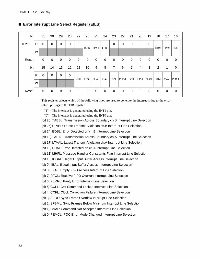
CHAPTER 2 FlexRay
■ Error Interrupt Line Select Register (EILS)
This register selects which of the following lines are used to generate the interrupts due to the error
interrupt flags in the EIR register.
"1" = The interrupt is generated using the INT1 pin.
"0" = The interrupt is generated using the INT0 pin.
[bit 26] TABBL: Transmission Across Boundary ch.B Interrupt Line Selection
[bit 25] LTVBL: Latest Transmit Violation ch.B Interrupt Line Selection
[bit 24] EDBL: Error Detected on ch.B Interrupt Line Selection
[bit 18] TABAL: Transmission Across Boundary ch.A Interrupt Line Selection
[bit 17] LTVAL: Latest Transmit Violation ch.A Interrupt Line Selection
[bit 16] EDAL: Error Detected on ch.A Interrupt Line Selection
[bit 11] MHFL: Message Handler Constraints Flag Interrupt Line Selection
[bit 10] IOBAL: Illegal Output Buffer Access Interrupt Line Selection
[bit 9] IIBAL: Illegal Input Buffer Access Interrupt Line Selection
[bit 8] EFAL: Empty FIFO Access Interrupt Line Selection
[bit 7] RFOL: Receive FIFO Overrun Interrupt Line Selection
[bit 6] PERRL: Parity Error Interrupt Line Selection
[bit 5] CCLL: CHI Command Locked Interrupt Line Selection
[bit 4] CCFL: Clock Correction Failure Interrupt Line Selection
[bit 3] SFOL: Sync Frame Overflow Interrupt Line Selection
[bit 2] SFBML: Sync Frames Below Minimum Interrupt Line Selection
[bit 1] CNAL: Command Not Accepted Interrupt Line Selection
[bit 0] PEMCL: POC Error Mode Changed Interrupt Line Selection
bit 31 30 29 28 27 26 25 24 23 22 21 20 19 18 17 16
0028H R 0 0 0 0 0TABBL LTVBL EDBL
0 0 0 0 0TABAL LTVAL EDAL
W
Reset 0 0 0 0 0 0 0 0 0 0 0 0 0 0 0 0
bit 15 14 13 12 11 10 9 8 7 6 5 4 3 2 1 0
R 0 0 0 0MHFL IOBAL IIBAL EFAL RFOL PERRL CCLL CCFL SFOL SFBML CNAL PEMCL
W
Reset 0 0 0 0 0 0 0 0 0 0 0 0 0 0 0 0
52
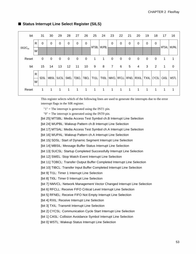
CHAPTER 2 FlexRay
■ Status Interrupt Line Select Register (SILS)
This register selects which of the following lines are used to generate the interrupts due to the error
interrupt flags in the SIR register.
"1" = The interrupt is generated using the INT1 pin.
"0" = The interrupt is generated using the INT0 pin.
[bit 25] MTSBL: Media Access Test Symbol ch.B Interrupt Line Selection
[bit 24] WUPBL: Wakeup Pattern ch.B Interrupt Line Selection
[bit 17] MTSAL: Media Access Test Symbol ch.A Interrupt Line Selection
[bit 16] WUPAL: Wakeup Pattern ch.A Interrupt Line Selection
[bit 15] SDSL: Start of Dynamic Segment Interrupt Line Selection
[bit 14] MBSIL: Message Buffer Status Interrupt Line Selection
[bit 13] SUCSL: Startup Completed Successfully Interrupt Line Selection
[bit 12] SWEL: Stop Watch Event Interrupt Line Selection
[bit 11] TOBCL: Transfer Output Buffer Completed Interrupt Line Selection
[bit 10] TIBCL: Transfer Input Buffer Completed Interrupt Line Selection
[bit 9] TI1L: Timer 1 Interrupt Line Selection
[bit 8] TI0L: Timer 0 Interrupt Line Selection
[bit 7] NMVCL: Network Management Vector Changed Interrupt Line Selection
[bit 6] RFCLL: Receive FIFO Critical Level Interrupt Line Selection
[bit 5] RFNEL: Receive FIFO Not Empty Interrupt Line Selection
[bit 4] RXIL: Receive Interrupt Line Selection
[bit 3] TXIL: Transmit Interrupt Line Selection
[bit 2] CYCSL: Communication Cycle Start Interrupt Line Selection
[bit 1] CASL: Collision Avoidance Symbol Interrupt Line Selection
[bit 0] WSTL: Wakeup Status Interrupt Line Selection
bit 31 30 29 28 27 26 25 24 23 22 21 20 19 18 17 16
002CH
R 0 0 0 0 0 0MTSBL WUPBL
0 0 0 0 0 0MTSAL WUPAL
W
Reset 0 0 0 0 0 0 1 1 0 0 0 0 0 0 1 1
bit 15 14 13 12 11 10 9 8 7 6 5 4 3 2 1 0
RSDSL MBSIL SUCSL SWEL TOBCL TIBCL TI1L TI0L NMVCL RFCLL RFNEL RXIL TXIL CYCSL CASL WSTL
W
Reset 1 1 1 1 1 1 1 1 1 1 1 1 1 1 1 1
53

CHAPTER 2 FlexRay
■ Error Interrupt Enable Set/Reset Registers (EIES, EIER)The configuration of these registers determines which status changes within the Error Interrupt Register
(EIR) generate an interrupt.
The interrupt enable flags can be enabled by writing "1" to address 0030H and disabled by writing "1" to
address 0034H. Writing "0" to either address does not change the enabled flags. The same value is read
from both registers (EIES/EIER). The value indicates the following meaning.
"1" = Interrupt enabled
"0" = Interrupt disabled
[bit 26] TABBE: Transmission Across Boundary ch.B Interrupt Enable Flag
[bit 25] LTVBE: Latest Transmit Violation ch.B Interrupt Enable Flag
[bit 24] EDBE: Error Detected on ch.B Interrupt Enable Flag
[bit 18] TABAE: Transmission Across Boundary ch.A Interrupt Enable Flag
[bit 17] LTVAE: Latest Transmit Violation ch.A Interrupt Enable Flag
[bit 16] EDAE: Error Detected on ch.A Interrupt Enable Flag
[bit 11] MHFE: Message Handler Constraints Flag Interrupt Enable Flag
[bit 10] IOBAE: Illegal Output Buffer Access Interrupt Enable Flag
[bit 9] IIBAE: Illegal Input Buffer Access Interrupt Enable Flag
[bit 8] EFAE: Empty FIFO Access Interrupt Enable Flag
[bit 7] RFOE: Receive FIFO Overrun Interrupt Enable Flag
[bit 6] PERRE: Parity Error Interrupt Enable Flag
[bit 5] CCLE: CHI Command Locked Interrupt Enable Flag
[bit 4] CCFE: Clock Correction Error Interrupt Enable Flag
[bit 3] SFOE: Sync Frame Overflow Interrupt Enable Flag
[bit 2] SFBME: Sync Frames Below Minimum Interrupt Enable Flag
[bit 1] CNAE: Command Not Accepted Interrupt Enable Flag
[bit 0]PEMCE: POC Error Mode Changed Interrupt Enable Flag
bit 31 30 29 28 27 26 25 24 23 22 21 20 19 18 17 16
0030H0034H
R 0 0 0 0 0TABBE LTVBE EDBE
0 0 0 0 0TABAE LTVAE EDAE
W
Reset 0 0 0 0 0 0 0 0 0 0 0 0 0 0 0 0
bit 15 14 13 12 11 10 9 8 7 6 5 4 3 2 1 0
R 0 0 0 0MHFE IOBAE IIBAE EFAE RFOE PERRE CCLE CCFE SFOE SFBME CNAE PEMCE
W
Reset 0 0 0 0 0 0 0 0 0 0 0 0 0 0 0 0
54
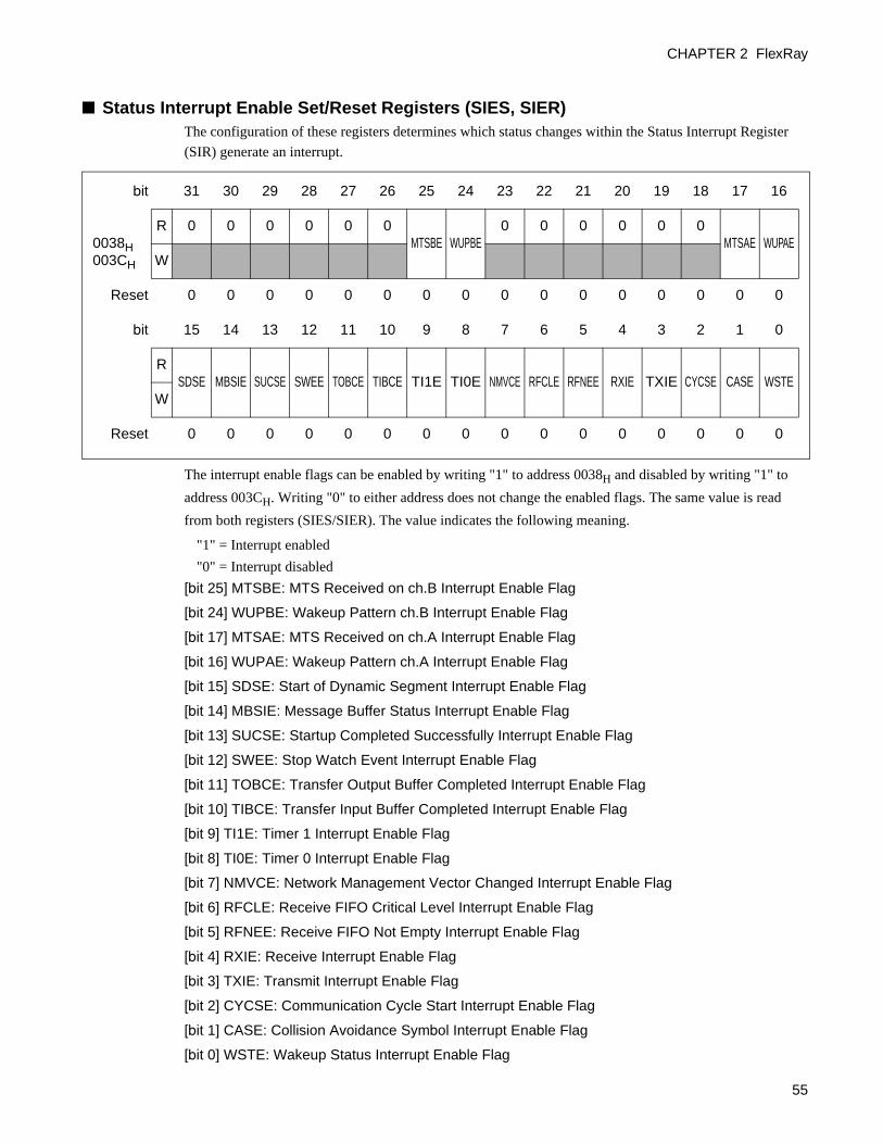
CHAPTER 2 FlexRay
■ Status Interrupt Enable Set/Reset Registers (SIES, SIER)The configuration of these registers determines which status changes within the Status Interrupt Register
(SIR) generate an interrupt.
The interrupt enable flags can be enabled by writing "1" to address 0038H and disabled by writing "1" to
address 003CH. Writing "0" to either address does not change the enabled flags. The same value is read
from both registers (SIES/SIER). The value indicates the following meaning.
"1" = Interrupt enabled
"0" = Interrupt disabled
[bit 25] MTSBE: MTS Received on ch.B Interrupt Enable Flag
[bit 24] WUPBE: Wakeup Pattern ch.B Interrupt Enable Flag
[bit 17] MTSAE: MTS Received on ch.A Interrupt Enable Flag
[bit 16] WUPAE: Wakeup Pattern ch.A Interrupt Enable Flag
[bit 15] SDSE: Start of Dynamic Segment Interrupt Enable Flag
[bit 14] MBSIE: Message Buffer Status Interrupt Enable Flag
[bit 13] SUCSE: Startup Completed Successfully Interrupt Enable Flag
[bit 12] SWEE: Stop Watch Event Interrupt Enable Flag
[bit 11] TOBCE: Transfer Output Buffer Completed Interrupt Enable Flag
[bit 10] TIBCE: Transfer Input Buffer Completed Interrupt Enable Flag
[bit 9] TI1E: Timer 1 Interrupt Enable Flag
[bit 8] TI0E: Timer 0 Interrupt Enable Flag
[bit 7] NMVCE: Network Management Vector Changed Interrupt Enable Flag
[bit 6] RFCLE: Receive FIFO Critical Level Interrupt Enable Flag
[bit 5] RFNEE: Receive FIFO Not Empty Interrupt Enable Flag
[bit 4] RXIE: Receive Interrupt Enable Flag
[bit 3] TXIE: Transmit Interrupt Enable Flag
[bit 2] CYCSE: Communication Cycle Start Interrupt Enable Flag
[bit 1] CASE: Collision Avoidance Symbol Interrupt Enable Flag
[bit 0] WSTE: Wakeup Status Interrupt Enable Flag
bit 31 30 29 28 27 26 25 24 23 22 21 20 19 18 17 16
0038H003CH
R 0 0 0 0 0 0MTSBE WUPBE
0 0 0 0 0 0MTSAE WUPAE
W
Reset 0 0 0 0 0 0 0 0 0 0 0 0 0 0 0 0
bit 15 14 13 12 11 10 9 8 7 6 5 4 3 2 1 0
RSDSE MBSIE SUCSE SWEE TOBCE TIBCE TI1E TI0E NMVCE RFCLE RFNEE RXIE TXIE CYCSE CASE WSTE
W
Reset 0 0 0 0 0 0 0 0 0 0 0 0 0 0 0 0
55

CHAPTER 2 FlexRay
■ Interrupt Line Enable Register (ILE)Interrupts can be enabled and disabled separately on the two interrupt lines (INT0 and INT1) by setting the
EINT0 and EINT1 bits to "1".
[bit 1] EINT1: Enable Interrupt Line 1
"1" = Interrupt line (INT1) enabled
"0" = Interrupt line (INT1) disabled
[bit 0] EINT0: Enable Interrupt Line 0
"1" = Interrupt line (INT0) enabled
"0" = Interrupt line (INT0) disabled
■ Timer 0 Configuration Register (T0C)Specifies the time that Timer 0 generates an interrupt in units of cycle counts and macroticks. When the
Timer 0 interrupt occurs, the INT2 interrupt output is set to "1" for a duration of 1 macrotick, and SIR:TI0
is also set to "1".
Timer 0 is able to operate when the POC is in the NORMAL_ACTIVE state or the NORMAL_PASSIVE
state. Timer 0 stops operating when the POC is in other states.
bit 31 30 29 28 27 26 25 24 23 22 21 20 19 18 17 16
0040H
R 0 0 0 0 0 0 0 0 0 0 0 0 0 0 0 0
W
Reset 0 0 0 0 0 0 0 0 0 0 0 0 0 0 0 0
bit 15 14 13 12 11 10 9 8 7 6 5 4 3 2 1 0
R 0 0 0 0 0 0 0 0 0 0 0 0 0 0EINT1 EINT0
W
Reset 0 0 0 0 0 0 0 0 0 0 0 0 0 0 0 0
56

CHAPTER 2 FlexRay
To reconfigure Timer 0, write "0" to the T0RC bit to stop the timer.
[bit 29 to bit 16] T0MO13 to T0MO0: Timer 0 Macrotick Offset Setting
Configures the Timer 0 interrupt generation offset time from the cycle configured in the cycle set. This offset time is specified in units of macroticks. The cycle set is configured using T0CC6 to T0CC0.
[bit 14 to bit 8] T0CC6 to T0CC0:Timer 0 Cycle Code Setting
Configures the cycle set that is used to generate the Timer 0 interrupt.
[bit 1] T0MS: Timer 0 Mode Select
"1" = Continuous mode
"0" = Single-shot mode
[bit 0] T0RC: Timer 0 Run Control
"1" = Timer 0 running
"0" = Timer 0 stopped
Note:
In the event of a state transition from the NORMAL_ACTIVE state or the NORMAL_PASSIVE state to another state, or if Timer 0 is stopped by clearing T0RC to "0", the INT2 interrupt output immediately outputs "L".
■ Timer 1 Configuration Register (T1C)The Timer 1 interrupt is generated when Timer 1 reaches the specified number of macroticks. When the
Timer 1 interrupt occurs, the interrupt output (INT3) is set to "1" for a duration of 1 macrotick, and SIR:TI1
is also set to "1".
Timer 1 is able to operate when the POC is in the NORMAL_ACTIVE state or the NORMAL_PASSIVE
state. Timer 1 stops operating when the POC is in other states.
bit 31 30 29 28 27 26 25 24 23 22 21 20 19 18 17 16
0044H
R 0 0T0MO13 T0MO12 T0MO11 T0MO10 T0MO9 T0MO8 T0MO7 T0MO6 T0MO5 T0MO4 T0MO3 T0MO2 T0MO1 T0MO0
W
Reset 0 0 0 0 0 0 0 0 0 0 0 0 0 0 0 0
bit 15 14 13 12 11 10 9 8 7 6 5 4 3 2 1 0
R 0T0CC6 T0CC5 T0CC4 T0CC3 T0CC2 T0CC1 T0CC0
0 0 0 0 0 0T0MS T0RC
W
Reset 0 0 0 0 0 0 0 0 0 0 0 0 0 0 0 0
57

CHAPTER 2 FlexRay
To reconfigure Timer 1, write a "0" to the T1RC bit to stop the timer.
[bit 29 to bit 16] T1MC13 to T1MC0:Timer 1 Macrotick Count
The Timer 1 interrupt is generated when Timer 1 matches the specified macrotick count. Timer 1 will not start if the specified macrotick count is outside of the permissible range.
Valid values: 2 to 16383 MT (continuous mode)
1 to 16383 MT (single-shot mode)
[bit 1] T1MS Timer 1 Mode Select
"1" = Continuous mode
"0" = Single-shot mode
[bit 0] T1RC Timer 1 Run Control
"1" = Timer 1 running
"0" = Timer 1 stopped
Note:
In the event of a state transition from the NORMAL_ACTIVE state or the NORMAL_PASSIVE state to another state, or if Timer 1 is stopped by clearing T1RC to "0", the interrupt output (INT3) immediately outputs "L".
bit 31 30 29 28 27 26 25 24 23 22 21 20 19 18 17 16
0048H
R 0 0T1MC13 T1MC12 T1MC11 T1MC10 T1MC9 T1MC8 T1MC7 T1MC6 T1MC5 T1MC4 T1MC3 T1MC2 T1MC1 T1MC0
W
Reset 0 0 0 0 0 0 0 0 0 0 0 0 0 0 1 0
bit 15 14 13 12 11 10 9 8 7 6 5 4 3 2 1 0
R 0 0 0 0 0 0 0 0 0 0 0 0 0 0T1MS T1RC
W
Reset 0 0 0 0 0 0 0 0 0 0 0 0 0 0 0 0
58

CHAPTER 2 FlexRay
■ Stop Watch Register 1 (STPW1)The stop watch is triggered under the following conditions.
- A rising or falling edge is input on the STPW pin
- Interrupt "0" or "1" is generated
- "1" is written to the SSWT bit
The macrotick counter addition begins after the stop watch has been activated. The actual cycle counter
value and macrotick value are stored in the stop watch registers. These values can be read by the host.
[bit 29 to bit 16] SMTV13 to SMTV0: Stopped Macrotick Value
The macrotick counter value when the stop watch event occurred. Valid values are in the range of 0 to 16000.
[bit 13 to bit 8] SCCV5 to SCCV0: Stopped Cycle Counter Value
The cycle counter value when the stop watch event occurred. Valid values are in the range of 0 to 63.
[bit 6] EINT1: Enable Interrupt 1 Trigger
If ESWT=1, the stop watch is triggered by interrupt 1 events.
"1" = Enabled
"0" = Disabled
[bit 5] EINT0: Enable Interrupt 0 Trigger
If ESWT=1, the stop watch is triggered by interrupt 0 events.
"1" = Enabled
"0" = Disabled
[bit 4] EETP: Enable External Trigger Pin
If ESWT=1, the stop watch is triggered by edge signals on the input pin (STPW).
"1" = Enabled
"0" = Disabled
[bit 3] SSWT: Software Stop Watch Trigger
The host can trigger the stop watch by setting this bit to "1". This bit is cleared to "0" after the actual cycle counter value and macrotick value are stored in the stop watch register.
This bit can be written to while ESWT=0.
bit 31 30 29 28 27 26 25 24 23 22 21 20 19 18 17 16
004CH
R 0 0 SMTV13 SMTV12 SMTV11 SMTV10 SMTV9 SMTV8 SMTV7 SMTV6 SMTV5 SMTV4 SMTV3 SMTV2 SMTV1 SMTV0
W
Reset 0 0 0 0 0 0 0 0 0 0 0 0 0 0 0 0
bit 15 14 13 12 11 10 9 8 7 6 5 4 3 2 1 0
R 0 0 SCCV5 SCCV4 SCCV3 SCCV2 SCCV1 SCCV0 0EINT1 EINT0 EETP SSWT EDGE SWMS ESWT
W
Reset 0 0 0 0 0 0 0 0 0 0 0 0 0 0 0 0
59

CHAPTER 2 FlexRay
"1" = The stop watch is triggered by the software trigger
"0" = The software trigger is cleared
[bit 2] EDGE: Stop Watch Trigger Edge Select
"1" = Rising edge
"0" = Falling edge
[bit 1] SWMS: Stop Watch Mode Select
"1" = Continuous
"0" = Single-shot
[bit 0] ESWT: Enable Stop Watch Trigger
When the stop watch is enabled, the stop watch is triggered by edge signals on the input pin (STPW), or by interrupts 0 or 1 (rising edge of INT0 or INT1). In single-shot mode, this bit is reset to "0" after the stop watch event occurs.
"1" = Enabled
"0" = Disabled
Note:
The ESWT bit and the SSWT bit cannot be set to "1" at the same time. The write access has no effect on the operation if this is attempted. Furthermore, both bits retain the values from prior to the write access. This applies irrespective of whether external stop watch triggers or software stop watch triggers are being used.
■ Stop Watch Register 2 (STPW2)The host is able to read the stop watch counter value of ch.A and ch.B.
[bit 26 to bit 16] SSCVB10 to SSCVB0: Stop Watch Counter Value ch.B
The value of the ch.B stop watch counter when the event occurred (0 to 2047)
[bit 10 to bit 0] SSCVA10 to SSCVA0: Stop Watch Counter Value ch.A
The value of the ch.A stop watch counter when the event occurred (0 to 2047)
bit 31 30 29 28 27 26 25 24 23 22 21 20 19 18 17 16
0050H
R 0 0 0 0 0 SSCVB10 SSCVB9 SSCVB8 SSCVB7 SSCVB6 SSCVB5 SSCVB4 SSCVB3 SSCVB2 SSCVB1 SSCVB0
W
Reset 0 0 0 0 0 0 0 0 0 0 0 0 0 0 0 0
bit 15 14 13 12 11 10 9 8 7 6 5 4 3 2 1 0
R 0 0 0 0 0 SSCVA10 SSCVA9 SSCVA8 SSCVA7 SSCVA6 SSCVA5 SSCVA4 SSCVA3 SSCVA2 SSCVA1 SSCVA0
W
Reset 0 0 0 0 0 0 0 0 0 0 0 0 0 0 0 0
60

CHAPTER 2 FlexRay
2.3.4 Communication Controller (CC) Control Registers
This section explains the bit configurations and functions of the communication controller (CC) control registers.
■ Communication Controller (CC) Control RegistersThis section explains the registers that control the FlexRay communication controller (CC). Under the
FlexRay protocol specifications, the application configuration data must set while in the CONFIG state.
Note that writes to the configuration registers are not locked while in the DEFAULT_CONFIG state.
When a hard reset is initiated, the controller changes to the DEFAULT_CONFIG state and each of the
registers are initialized. The protocol operation controller (POC) sets CMD3 to CMD0 = 0001B (CHI
command CONFIG) to change from the DEFAULT_CONFIG state to the CONFIG state. Follow the
procedure described in "■ Lock Register (LCK)" to change from the CONFIG state to the READY state.
All of the bits marked with an asterisk (*) can only be updated in the DEFAULT_CONFIG or CONFIG
states.
■ SUC Configuration Register 1 (SUCC1)
[bit 27] CCHB: Connected to ch.B (pChannels)
Specifies whether or not the node is connected to ch.B.
"1" = The node is connected to ch.B
"0" = The node is not connected to ch.B
[bit 26] CCHA: Connected to ch.A (pChannels)
Specifies whether or not the node is connected to ch.A.
"1" = The node is connected to ch.A
"0" = The node is not connected to ch.A
bit 31 30 29 28 27 26 25 24 23 22 21 20 19 18 17 16
0080H
R 0 0 0 0CCHB* CCHA* MTSB* MTSA* HCSE* TSM* WUCS* PTA4* PTA3* PTA2* PTA1* PTA0*
W
Reset 0 0 0 0 1 1 0 0 0 1 0 0 0 0 0 0
bit 15 14 13 12 11 10 9 8 7 6 5 4 3 2 1 0
RCSA4* CSA3* CSA2* CSA1* CSA0*
0TXSY* TXST*
PBSY 0 0 0CMD3 CMD2 CMD1 CMD0
W
Reset 0 0 0 1 0 0 0 0 0 0 0 0 0 0 0 0
61
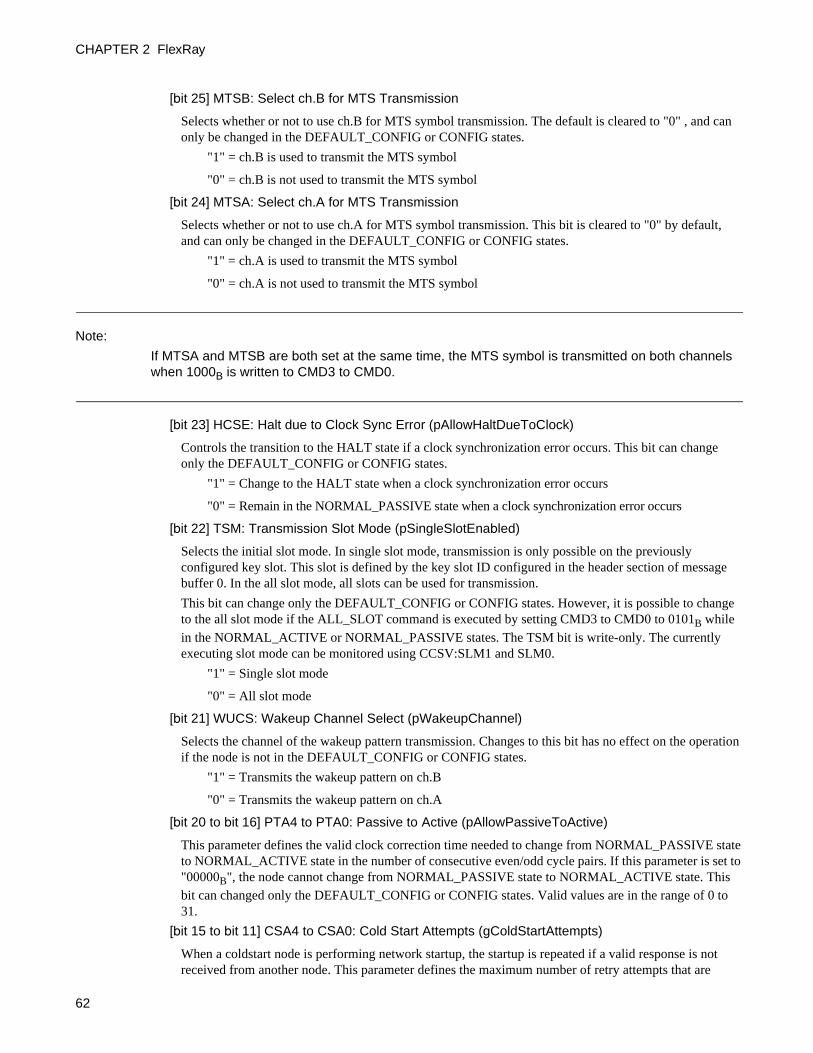
CHAPTER 2 FlexRay
[bit 25] MTSB: Select ch.B for MTS Transmission
Selects whether or not to use ch.B for MTS symbol transmission. The default is cleared to "0" , and can only be changed in the DEFAULT_CONFIG or CONFIG states.
"1" = ch.B is used to transmit the MTS symbol
"0" = ch.B is not used to transmit the MTS symbol
[bit 24] MTSA: Select ch.A for MTS Transmission
Selects whether or not to use ch.A for MTS symbol transmission. This bit is cleared to "0" by default, and can only be changed in the DEFAULT_CONFIG or CONFIG states.
"1" = ch.A is used to transmit the MTS symbol
"0" = ch.A is not used to transmit the MTS symbol
Note:
If MTSA and MTSB are both set at the same time, the MTS symbol is transmitted on both channels when 1000B is written to CMD3 to CMD0.
[bit 23] HCSE: Halt due to Clock Sync Error (pAllowHaltDueToClock)
Controls the transition to the HALT state if a clock synchronization error occurs. This bit can change only the DEFAULT_CONFIG or CONFIG states.
"1" = Change to the HALT state when a clock synchronization error occurs
"0" = Remain in the NORMAL_PASSIVE state when a clock synchronization error occurs
[bit 22] TSM: Transmission Slot Mode (pSingleSlotEnabled)
Selects the initial slot mode. In single slot mode, transmission is only possible on the previously configured key slot. This slot is defined by the key slot ID configured in the header section of message buffer 0. In the all slot mode, all slots can be used for transmission.
This bit can change only the DEFAULT_CONFIG or CONFIG states. However, it is possible to change to the all slot mode if the ALL_SLOT command is executed by setting CMD3 to CMD0 to 0101B while in the NORMAL_ACTIVE or NORMAL_PASSIVE states. The TSM bit is write-only. The currently executing slot mode can be monitored using CCSV:SLM1 and SLM0.
"1" = Single slot mode
"0" = All slot mode
[bit 21] WUCS: Wakeup Channel Select (pWakeupChannel)
Selects the channel of the wakeup pattern transmission. Changes to this bit has no effect on the operation if the node is not in the DEFAULT_CONFIG or CONFIG states.
"1" = Transmits the wakeup pattern on ch.B
"0" = Transmits the wakeup pattern on ch.A
[bit 20 to bit 16] PTA4 to PTA0: Passive to Active (pAllowPassiveToActive)
This parameter defines the valid clock correction time needed to change from NORMAL_PASSIVE state to NORMAL_ACTIVE state in the number of consecutive even/odd cycle pairs. If this parameter is set to "00000B", the node cannot change from NORMAL_PASSIVE state to NORMAL_ACTIVE state. This bit can changed only the DEFAULT_CONFIG or CONFIG states. Valid values are in the range of 0 to 31.
[bit 15 to bit 11] CSA4 to CSA0: Cold Start Attempts (gColdStartAttempts)
When a coldstart node is performing network startup, the startup is repeated if a valid response is not received from another node. This parameter defines the maximum number of retry attempts that are
62

CHAPTER 2 FlexRay
allowed. This value can change only the DEFAULT_CONFIG or CONFIG states. Set this parameter to the same value on all of the nodes in a cluster. Valid values are in the range of 2 to 31.
[bit 9] TXSY: Transmit Sync Frame in Key Slot (pKeySlotUsedForSync)
Determines whether or not the key slot is used to transmit a sync frame. This bit can change only the DEFAULT_CONFIG or CONFIG states.
"1" = The key slot is used to transmit a sync frame. The node is in sync.
"0" = The key slot is not used to transmit a sync frame. The node is not in coldstart or sync.
[bit 8] TXST: Transmit Startup Frame in Key Slot (pKeySlotUsedForStartup)
Determines whether or not the key slot is used to transmit a startup frame. This bit can change only the DEFAULT_CONFIG or CONFIG states.
"1" = The key slot is used to transmit a startup frame. The node is in coldstart.
"0" = The key slot is not used to transmit a startup frame. The node is not in coldstart.
Note:
Set both the TXST and TXSY bits to "1" to transmit a startup frame.
[bit 7] PBSY: POC Busy
This flag indicates that the POC is busy and is unable to receive commands. When PBSY=1, CMD3 to CMD0 are locked against write accesses. After a hardware reset, this flag is set to "1" during initialization of the internal RAM.
"1" = POC busy. CMD3 to CMD0 are locked
"0" = POC idle. CMD3 to CMD0 are writable
[bit 3 to bit 0] CMD3 to CMD0: CHI Command Vector
Although this CHI command vector is always writable, particular commands are only valid in particular POC states. If a command is invalid, the CHI command vectors CMD3 to CMD0 are reset to "0000B" (command_not_accepted) and EIR:CNA is set to "1" without executing the command. The CHI command needs to be repeated if EIR:CCL and EIR:CNA are both set to "1". If a command to change to a particular POC state is given while the device is already in that POC state, the command has no effect on the operation.
0000 = command_not_accepted
0001 = CONFIG
0010 = READY
0011 = WAKEUP
0100 = RUN
0101 = ALL_SLOTS
0110 = HALT
0111 = FREEZE
1000 = SEND_MTS
1001 = ALLOW_COLDSTART
1010 = RESET_STATUS_INDICATORS
1011 = MONITOR_MODE
1100 = CLEAR_RAMS
1101 = reserved
1110 = reserved
1111 = reserved
63

CHAPTER 2 FlexRay
Reading CMD3 to CMD0 returns the most recently accepted CHI command. The actual POC state can be monitored using CCSV:POCS5 to POCS0. The "reserved" CHI commands are used by hardware test functions.
command_not_accepted
Writing CMD3 to CMD0 = 0000B will reset CMD3 to CMD0 = 0000B under any of the following conditions.
- An invalid command is specified
- A command is specified during the internal POC state change period
- A new command is specified while a CHI command is executing
- command_not_accepted is specified
If a command is invalid, the CHI command vectors CMD3 to CMD0 are reset to "0000B" (command_not_accepted) and EIR:CNA is set to "1" without executing the command. An interrupt is generated if interrupts are enabled.
CONFIG
If CMD3 to CMD0 are set to 0001B while in the DEFAULT_CONFIG, READY, or MONITOR_MODE states, the device changes to the CONFIG state. If CMD3 to CMD0 are set to 0001B while in the HALT state, the device changes to the DEFAULT_CONFIG state. If CMD3 to CMD0 are set to 0001B while in any other state, CMD3 to CMD0 are reset to 0000B (command_not_accepted).
READY
If CMD3 to CMD0 are set to 0010B while in the CONFIG, NORMAL_ACTIVE, NORMAL_PASSIVE, STARTUP, or WAKEUP states, the device changes to the READY state. If CMD3 to CMD0 are set to 0010B while in any other state, CMD3 to CMD0 are reset to 0000B (command_not_accepted).
WAKEUP
If CMD3 to CMD0 are set to 0011B while in the READY state, the device changes to the WAKEUP state. If CMD3 to CMD0 are set to 0011B while in any other state, CMD3 to CMD0 are reset to 0000B (command_not_accepted).
RUN
If CMD3 to CMD0 are set to 0100B while in the READY state, the device changes to the STARTUP state. If CMD3 to CMD0 are set to 0100B while in any other state, CMD3 to CMD0 are reset to 0000B (command_not_accepted).
ALL_SLOTS
If CMD3 to CMD0 are set to 0101B while in the NORMAL_ACTIVE or NORMAL_PASSIVE states, the device changes from single slot mode to all slot mode after successfully completing the startup/integration in the completion following the present cycle. If CMD3 to CMD0 are set to 0101B while in any other state, CMD3 to CMD0 are reset to 0000B (command_not_accepted).
HALT
If CMD3 to CMD0 are set to 0110B while in the NORMAL_ACTIVE or NORMAL_PASSIVE states, the halt request bit CCSV:HRQ is set to "1", and the device changes to the HALT state in the completion following the present cycle. If CMD3 to CMD0 are set to 0110B while in any other state, CMD3 to CMD0 are reset to 0000B (command_not_accepted).
FREEZE
If CMD3 to CMD0 are set to 0111B, the freeze status indicator CCSV:FSI is set to "1" and the device immediately enters the HALT state. This command can be set while in any state.
64
CHAPTER 2 FlexRay
SEND_MTS
If CMD3 to CMD0 are set to 1000B while in the NORMAL_ACTIVE state after setting the all slot mode (CCSV:SLM1, SLM0 = 11B), a single MTS symbol is transmitted on the channels specified by MTSA and MTSB during the following symbol window. If CMD3 to CMD0 are set to 1000B while in any other state, CMD3 to CMD0 are reset to 0000B (command_not_accepted).
ALLOW_COLDSTART
If CMD3 to CMD0 are set to 1001B while in a state other than the DEFAULT_CONFIG, CONFIG, and HALT states, the CCSV:CSI bit should be cleared to "0" to enable the node coldstart. If CMD3 to CMD0 are set to 1001B while in the DEFAULT_CONFIG, CONFIG, or HALT states, CMD3 to CMD0 are reset to 0000B (command_not_accepted). TXST and TXSY both also need to be set in order to enable coldstart.
RESET_STATUS_INDICATORS
If CMD3 to CMD0 are set to 1010B, all of the CCSV:FSI, HRQ, CSNI, and CSAI status flags are reset. This command can be set while in any state.
CLEAR_RAMS
If CMD3 to CMD0 are set to 1100B while in the DEFAULT_CONFIG or CONFIG states, MHDS:CRAM is set to "1". If CMD3 to CMD0 are set to 1100B while in any other state, CMD3 to CMD0 are reset to 0000B (command_not_accepted). MHDS:CRAM is also set to "1" after a hardware reset. All of the internal RAM blocks are initialized to zero by setting MHDS:CRAM to "1". During the RAM initialization, PBSY indicates POC busy.
Initialization of the internal RAM blocks of the FlexRay controller requires 2048 f_bclk cycles (configuration of f_bclk is performed using CCNT:RCLK. See "■ Version Information Register (VER)"). After a hardware reset, or after setting CMD3 to CMD0 to 1100B (CHI command CLEAR_RAMS), do not access the IBF or OBF while the internal RAM block is being initialized.
Before setting CMD3 to CMD0 to 1100B, verify that there are no transfer in progress between the message RAM and the IBF/OBF.
This setting resets the message buffer status registers (MHDS, TXRQ1, TXRQ2, TXRQ3, TXRQ4, NDAT1, NDAT2, NDAT3, NDAT4, MBSC1, MBSC2, MBSC3, and MBSC4).
Note:
The configuration registers and status registers can be accessed while the CHI command CLEAR_RAMS (CMD3 to CMD0 = 1100B) is executing.
MONITOR_MODE
If CMD3 to CMD0 are set to 1011B while in the CONFIG state, the device changes to the MONITOR_MODE state. In this mode, FlexRay frames and CAS/MTS symbols can be received, and coding errors can also be detected. However, the time of the received frames is not checked. This mode can be used for debugging purposes. For example, this mode can be used if the FlexRay network startup was failed to analyze the cause of the failure. If CMD3 to CMD0 are set to 1011B while in any other state, CMD3 to CMD0 are reset to 0000B (command_not_accepted).
65

CHAPTER 2 FlexRay
■ SUC Configuration Register 2 (SUCC2)This register can only be changed in the DEFAULT_CONFIG or CONFIG states.
[bit 27 to bit 24] LTN3 to LTN0: Listen Timeout Noise (gListenNoise-1)
This value specifies the upper limit on the startup and wakeup listen timeout used in an environment where noise occurs as a multiplier of listen timeout.Valid values are in the range of 2 to 16. Set LTN3 to LTN0 to the same value in every node in the cluster.
[bit 20 to bit 0] LT20 to LT0: Listen Timeout (pdListenTimeout)
Specifies the startup and wakeup listen timeout in units of µT. Valid values are in the range of 1284 to 1283846 µT.
Note:
The length of time of the wakeup and startup noise timeout is calculated as follows.
Listen Timeout × Listen Timeout Noise = [LT20 to LT0] × ([LTN3 to LTN0] + 1)
■ SUC Configuration Register 3 (SUCC3)This register can only be changed in the DEFAULT_CONFIG or CONFIG states.
bit 31 30 29 28 27 26 25 24 23 22 21 20 19 18 17 16
0084H
R 0 0 0 0LTN3* LTN2* LTN1* LTN0*
0 0 0LT20* LT19* LT18* LT17* LT16*
W
Reset 0 0 0 0 0 0 0 1 0 0 0 0 0 0 0 0
bit 15 14 13 12 11 10 9 8 7 6 5 4 3 2 1 0
RLT 15* LT 14* LT 13* LT 12* LT 11* LT 10* LT9* LT8* LT7* LT6* LT5* LT4* LT3* LT2* LT1* LT0*
W
Reset 0 0 0 0 0 1 0 1 0 0 0 0 0 1 0 0
bit 31 30 29 28 27 26 25 24 23 22 21 20 19 18 17 16
0088H
R 0 0 0 0 0 0 0 0 0 0 0 0 0 0 0 0
W
Reset 0 0 0 0 0 0 0 0 0 0 0 0 0 0 0 0
bit 15 14 13 12 11 10 9 8 7 6 5 4 3 2 1 0
R 0 0 0 0 0 0 0 0WCF3* WCF2* WCF1* WCF0* WCP3* WCP2* WCP1* WCP0*
W
Reset 0 0 0 0 0 0 0 0 0 0 0 1 0 0 0 1
66
CHAPTER 2 FlexRay
[bit 7 to bit 4] WCF3 to WCF0: Maximum Time Without Clock Correction HALT (gMaxWithoutClockCorrectionFatal)
This parameter defines the clock correction failure that triggers a state transition from the NORMAL_ACTIVE or NORMAL_PASSIVE states to the HALT state in the number of consecutive even/odd cycle pairs. Set this parameter to the same value on all of the nodes in a cluster. Valid values are in the range of 1 to 15 cycle pairs.
[bit 3 to bit 0] WCP3 to WCP0: Maximum Time Without Clock Correction Passive (gMaxWithoutClockCorrectionPassive)
This parameter defines the clock correction failure that triggers a state transition from the NORMAL_ACTIVE state to the NORMAL_PASSIVE state in the number of consecutive even/odd cycle pairs. Set this parameter to the same value on all of the nodes in a cluster. Valid values are in the range of 1 to 15 cycle pairs.
■ NEM Configuration Register (NEMC)This register can only be changed in the DEFAULT_CONFIG or CONFIG states.
[bit 3 to bit 0] NML3 to NML0: Network Management Vector Length (gNetworkManagementVectorLength)
These bits set the length of the network management vector. All of the nodes in a cluster should be set to the same configuration length. Valid values are in the range of 0 to 12.
bit 31 30 29 28 27 26 25 24 23 22 21 20 19 18 17 16
008CH
R 0 0 0 0 0 0 0 0 0 0 0 0 0 0 0 0
W
Reset 0 0 0 0 0 0 0 0 0 0 0 0 0 0 0 0
bit 15 14 13 12 11 10 9 8 7 6 5 4 3 2 1 0
R 0 0 0 0 0 0 0 0 0 0 0 0NML3* NML2* NML1* NML0*
W
Reset 0 0 0 0 0 0 0 0 0 0 0 0 0 0 0 0
67

CHAPTER 2 FlexRay
■ PRT Configuration Register 1 (PRTC1)This register can only be changed in the DEFAULT_CONFIG or CONFIG states.
[bit 31 to bit 26] RWP5 to RWP0: Transmission Counts of Wakeup Pattern (pWakeupPattern)
Sets the number of times to transmit the wakeup symbol. Valid values are in the range of 2 to 63.
[bit 24 to bit 16] RXW8 to RXW0: Wakeup Symbol Receive Window Length (gdWakeupSymbolRxWindow)
Sets the length of the window for the node to receive the wakeup pattern as a number of bit-times. Set this parameter to the same value on all of the nodes in a cluster. Valid values are in the range of 76 to 301.
[bit 15, bit 14] BRP1, BRP0: Baud Rate Prescaler (gdSampleClockPeriod, pSamplePerMicrotick)
Sets the baud rate on the FlexRay bus. The duration of one bit is always composed of 8 samples. The
sample clock f_sclk* is configured using CCNT:SDIV1 and SDIV0. See "2.6.2 Setting Example of the FlexRay Baud Rate" for detailed examples of baud rate settings.
"00B":
gdSampleClockPeriod = 1/f_sclk(s)
pSamplesPerMicrotick = 2
"01B":
gdSampleClockPeriod = 2/f_sclk(s)
pSamplesPerMicrotick = 1
"10B", "11B":
gdSampleClockPeriod = 4/f_sclk(s)
pSamplesPerMicrotick = 1
*: See "2.6 FlexRay Controller Clock".
[bit 13, bit 12] SPP1, SPP0: Strobe Point Position
This parameter defines the number of sample counts. Sampling is performed the number of times as defined by SPP1 and SPP0, and the value of the bit ("H"/"L") is determined from the majority of the sampled values ("H"/"L") measured in this way.
"00B", "11B" = 5 samples
"01B" = 4 samples
bit 31 30 29 28 27 26 25 24 23 22 21 20 19 18 17 16
0090H
RRWP5* RWP4* RWP3* RWP2* RWP1* RWP0*
0RXW8* RXW7* RXW6* RXW5* RXW4* RXW3* RXW2* RXW1* RXW0*
W
Reset 0 0 0 0 1 0 0 0 0 1 0 0 1 1 0 0
bit 15 14 13 12 11 10 9 8 7 6 5 4 3 2 1 0
RBRP1* BRP0* SPP1* SPP0*
0 CASM6CASM5* CASM4* CASM3* CASM2* CASM1* CASM0* TSST3* TSST2* TSST1* TSST0*
W
Reset 0 0 0 0 0 1 1 0 0 0 1 1 0 0 1 1
68

CHAPTER 2 FlexRay
"10B" = 6 samples
[bit 10 to bit 4] CASM6 to CASM0: Collision Avoidance Symbol Max (gdCASRxLowMax)
This parameter defines the upper limit on the length of the acceptance window used for the collision avoidance symbol (CAS). CASM bit 6 is fixed at "1". Valid values are in the range of 67 to 99.
[bit 3 to bit 0] TSST3 to TSST0: Transmission Start Sequence Transmitter (gdTSSTransmitter)
This parameter defines the duration of the transmission start sequence (TSS) in units of bit-time (1 bit-time = 4 µT = 100ns@10Mbps). Set this parameter to the same value on all of the nodes in a cluster. Valid values are in the range of 3 to 15.
*: See "2.6 FlexRay Controller Clock".
■ PRT Configuration Register 2 (PRTC2)This register can change only the DEFAULT_CONFIG or CONFIG states.
[bit 29 to bit 24] TXL5 to TXL0: Wakeup Symbol Transmit "L" Time(gdWakeupSymbolTxLow)
Sets the length of the "L" time for the node to transmit the wakeup symbol as a number of bit-times. Set this parameter to the same value on all of the nodes in a cluster. Valid values are in the range of 15 to 60.
[bit 23 to bit 16] TXI7 to TXI0: Wakeup Symbol Transmit Idle Phase Time (gdWakeupSymbolIdle)
Sets the length of the idle phase for the node to transmit the wakeup symbol as a number of bit-times. Set this parameter to the same value on all of the nodes in a cluster. Valid values are in the range of 45 to 180.
[bit 13 to bit 8] RXL5 to RXL0: Wakeup Symbol Receive "L" Time (gdWakeupSymbolRxLow)
Sets the length of the "L" time for the node to receive the wakeup symbol as a number of bit-times. Set this parameter to the same value on all of the nodes in a cluster. Valid values are in the range of 10 to 55.
[bit 5 to bit 0] RXI5 to RXI0: Wakeup Symbol Receive Idle Phase Time (gdWakeupSymbolRxIdle)
Sets the length of the idle phase for the node to receive the wakeup symbol as a number of bit-times. Set this parameter to the same value on all of the nodes in a cluster. Valid values are in the range of 14 to 59.
bit 31 30 29 28 27 26 25 24 23 22 21 20 19 18 17 16
0094H
R 0 0TXL5* TXL4* TXL3* TXL2* TXL1* TXL0* TXI7* TXI6* TXI5* TXI4* TXI3* TXI2* TXI1* TXI0*
W
Reset 0 0 0 0 1 1 1 1 0 0 1 0 1 1 0 1
bit 15 14 13 12 11 10 9 8 7 6 5 4 3 2 1 0
R 0 0RXL5* RXL4* RXL3* RXL2* RXL1* RXL0*
0 0RXI5* RXI4* RXI3* RXI2* RXI1* RXI0*
W
Reset 0 0 0 0 1 0 1 0 0 0 0 0 1 1 1 0
69
CHAPTER 2 FlexRay
■ MHD Configuration Register (MHDC)This register can only be changed in the DEFAULT_CONFIG or CONFIG states.
[bit 28 to bit 16] SLT12 to SLT0: Start of Latest Transmit (pLatestTx)
Sets the maximum value of the minislot immediately before transmission of frames in the dynamic segment is disabled. If SLT12 to SLT0 is set to "0", data is not transmitted in the dynamic segment. Valid values are in the range of 0 to 7981.
[bit 6 to bit 0] SFDL6 to SFDL0: Static Frame Data Length (gPayloadLengthStatic)
Sets the payload length for the entire cluster for all frames transmitted in the static segment. The actual payload length is 2 times the value of these bits in bytes. Set the payload length to the same value on all of the nodes in a cluster. Valid values are in the range of 0 to 127.
■ GTU Configuration Register 1 (GTUC1)This register can change only the DEFAULT_CONFIG or CONFIG states.
[bit 19 to bit 0] UT19 to UT0: Microticks per Cycle (gMicroPerCycle)
Sets the number of microticks in a communication cycle. Valid values are in the range of 640 to 640000 µT.
bit 31 30 29 28 27 26 25 24 23 22 21 20 19 18 17 16
0098H
R 0 0 0SLT12* SLT11* SLT10* SLT9* SLT8* SLT7* SLT6* SLT5* SLT4* SLT3* SLT2* SLT1* SLT0*
W
Reset 0 0 0 0 0 0 0 0 0 0 0 0 0 0 0 0
bit 15 14 13 12 11 10 9 8 7 6 5 4 3 2 1 0
R 0 0 0 0 0 0 0 0 0SFDL6* SFDL5* SFDL4* SFDL3* SFDL2* SFDL1* SFDL0*
W
Reset 0 0 0 0 0 0 0 0 0 0 0 0 0 0 0 0
bit 31 30 29 28 27 26 25 24 23 22 21 20 19 18 17 16
00A0H
R 0 0 0 0 0 0 0 0 0 0 0 0UT19* UT18* UT17* UT16*
W
Reset 0 0 0 0 0 0 0 0 0 0 0 0 0 0 0 0
bit 15 14 13 12 11 10 9 8 7 6 5 4 3 2 1 0
RUT15* UT14* UT13* UT12* UT11* UT10* UT9* UT8* UT7* UT6* UT5* UT4* UT3* UT2* UT1* UT0*
W
Reset 0 0 0 0 0 0 1 0 1 0 0 0 0 0 0 0
70

CHAPTER 2 FlexRay
■ GTU Configuration Register 2 (GTUC2)This register can only be changed in the DEFAULT_CONFIG or CONFIG states.
[bit 19 to bit 16] SNM3 to SNM0: Sync Node Max (gSyncNodeMax)
Sets the maximum number of nodes that transmit sync frames (frames where the sync frame indicator SYN is set to "1"). Set this parameter to the same value on all of the nodes in a cluster. Valid values are in the range of 2 to 15.
[bit 13 to bit 0] MPC13 to MPC0: Macroticks per Cycle (gMacroPerCycle)
Sets the number of macroticks in a communication cycle. Set the cycle length to the same value on all of the nodes in a cluster. Valid values are in the range of 10 to 16000 MT.
■ GTU Configuration Register 3 (GTUC3)This register can change only the DEFAULT_CONFIG or CONFIG states.
[bit 30 to bit 24] MIOB6 to MIOB0: Macrotick Initial Offset ch.B (pMacroInitialOffset[B])
This parameter sets the number of macroticks between the macrotick boundary after the ch.B secondary time reference point and the static slot boundary.This value is based on the nominal macrotick time length. Set this parameter to the same value on all of the nodes in a cluster. Valid values are in the range of 2 to 72 MT.
bit 31 30 29 28 27 26 25 24 23 22 21 20 19 18 17 16
00A4H
R 0 0 0 0 0 0 0 0 0 0 0 0SNM3* SNM2* SNM1* SNM0*
W
Reset 0 0 0 0 0 0 0 0 0 0 0 0 0 0 1 0
bit 15 14 13 12 11 10 9 8 7 6 5 4 3 2 1 0
R 0 0MPC13* MPC12* MPC11* MPC10* MPC9* MPC8* MPC7* MPC6* MPC5* MPC4* MPC3* MPC2* MPC1* MPC0*
W
Reset 0 0 0 0 0 0 0 0 0 0 0 0 1 0 1 0
bit 31 30 29 28 27 26 25 24 23 22 21 20 19 18 17 16
00A8H
R 0MIOB6* MIOB5* MIOB4* MIOB3* MIOB2* MIOB1* MIOB0*
0MIOA6* MIOA5* MIOA4* MIOA3* MIOA2* MIOA1* MIOA0*
W
Reset 0 0 0 0 0 0 1 0 0 0 0 0 0 0 1 0
bit 15 14 13 12 11 10 9 8 7 6 5 4 3 2 1 0
RUIOB7* UIOB6* UIOB5* UIOB4* UIOB3* UIOB2* UIOB1* UIOB0* UIOA7* UIOA6* UIOA5* UIOA4* UIOA3* UIOA2* UIOA1* UIOA0*
W
Reset 0 0 0 0 0 0 0 0 0 0 0 0 0 0 0 0
71

CHAPTER 2 FlexRay
[bit 22 to bit 16] MIOA6 to MIOA0: Macrotick Initial Offset ch.A (pMacroInitialOffset[A])
This parameter sets the number of macroticks between the macrotick boundary after the ch.A secondary time reference point and the static slot boundary. This value is based on the nominal macrotick time length. Set this parameter to the same value on all of the nodes in a cluster. Valid values are in the range of 2 to 72 MT.
[bit 15 to bit 8] UIOB7 to UIOB0: Microtick Initial Offset ch.B (pMicroInitialOffset[B])
This parameter sets the number of microticks between the macrotick boundary after the ch.B secondary time reference point and the real time reference point. This parameter depends on Delay Compensation ch.B, and needs to be set independently for each channel. Valid values are in the range of 0 to 240 µT.
[bit 7 to bit 0] UIOA7 to UIOA0: Microtick Initial Offset ch.A (pMicroInitialOffset[A])
This parameter sets the number of microticks between the macrotick boundary after the ch.A secondary time reference point and the real time reference point. This parameter depends on Delay Compensation ch.A, and needs to be set independently for each channel. Valid values are in the range of 0 to 240 µT.
■ GTU Configuration Register 4 (GTUC4)This register can only be changed in the DEFAULT_CONFIG or CONFIG states. See "■ Starting NIT and
Configuring the Offset Correction Start" for details on setting NIT13 to NIT0 and OCS13 to OCS0.
[bit 29 to bit 16] OCS13 to OCS0: Offset Correction Start (gOffsetCorrectionStart-1)
This parameter determines the offset correction start position within the NIT phase. The position is calculated by counting from the cycle start position. Set this parameter to the same value on all of the nodes in a cluster. Valid values are in the range of 8 to 15998 MT.
[bit 13 to bit 0] NIT13 to NIT0: Network Idle Time Start (gMacroPerCycle-gdNIT-1)
This parameter sets the start point of the network idle time (NIT) at the end of the communication cycle as the number of macroticks.
Macrotick = gMacroPerCycle - gdNIT - 1
The NIT starts when the above equation is satisfied. Set this parameter to the same value on all of the nodes in a cluster. Valid values are in the range of 7 to 15997 MT.
bit 31 30 29 28 27 26 25 24 23 22 21 20 19 18 17 16
00ACH
R 0 0OCS13* OCS12* OCS11* OCS10* OCS9* OCS8* OCS7* OCS6* OCS5* OCS4* OCS3* OCS2* OCS1* OCS0*
W
Reset 0 0 0 0 0 0 0 0 0 0 0 0 1 0 0 0
bit 15 14 13 12 11 10 9 8 7 6 5 4 3 2 1 0
R 0 0NIT13* NIT12* NIT11* NIT10* NIT9* NIT8* NIT7* NIT6* NIT5* NIT4* NIT3* NIT2* NIT1* NIT0*
W
Reset 0 0 0 0 0 0 0 0 0 0 0 0 0 1 1 1
72
CHAPTER 2 FlexRay
■ GTU Configuration Register 5 (GTUC5)This register can only be changed in the DEFAULT_CONFIG or CONFIG states.
[bit 31 to bit 24] DEC7 to DEC0: Decoding Correction (pDecodingCorrection)
This parameter sets the decoding correction value that is used to determine the primary time reference point. Valid values are in the range of 14 to 143 µT.
[bit 20 to bit 16] CDD4 to CDD0: Cluster Drift Damping (pClusterDriftDamping)
This parameter sets the cluster drift damping that is used during clock synchronization to minimize the accumulated drift. Valid values are in the range of 0 to 20 µT.
[bit 15 to bit 8] DCB7 to DCB0: Delay Compensation Ch.B (pDelayCompensation[B])
This parameter is used for compensating the receive delay on ch.B. This parameter is guaranteed up to the cPropagationDelayMax parameter that sets in units of microticks the expected propagation delay in the range of 0.0125 to 0.05 µs. In practice, use the length of the minimum propagation delay across all of the synchronized nodes. Valid values are in the range of 0 to 200 µT.
[bit 7 to bit 0] DCA7 to DCA0: Delay Compensation Ch.A (pDelayCompensation[A])
This parameter is used for compensating the receive delay on ch.A. This parameter is guaranteed up to the cPropagationDelayMax parameter that sets in units of microticks the expected propagation delay in the range of 0.0125 to 0.05 µs. In practice, use the length of the minimum propagation delay across all of the synchronized nodes. Valid values are in the range of 0 to 200 µT.
bit 31 30 29 28 27 26 25 24 23 22 21 20 19 18 17 16
00B0H
RDEC7* DEC6* DEC5* DEC4* DEC3* DEC2* DEC1* DEC0*
0 0 0CDD4* CDD3* CDD2* CDD1* CDD0*
W
Reset 0 0 0 0 1 1 1 0 0 0 0 0 0 0 0 0
bit 15 14 13 12 11 10 9 8 7 6 5 4 3 2 1 0
RDCB7* DCB6* DCB5* DCB4* DCB3* DCB2* DCB1* DCB0* DCA7* DCA6* DCA5* DCA4* DCA3* DCA2* DCA1* DCA0*
W
Reset 0 0 0 0 0 0 0 0 0 0 0 0 0 0 0 0
73

CHAPTER 2 FlexRay
■ GTU Configuration Register 6 (GTUC6)This register can change only the DEFAULT_CONFIG or CONFIG states.
[bit 26 to bit 16] MOD10 to MOD0: Maximum Oscillator Drift (pdMaxDrift)
This parameter sets the maximum drift offset between 2 asynchronous nodes in a single communication cycle in units of µT. Valid values are in the range of 2 to 1923 µT.
[bit 10 to bit 0] ASR10 to ASR0: Accepted Startup Range (pdAcceptedStartupRange)
This parameter sets the extended range of measurement error of the startup frame as a number of microticks. Valid values are in the range of 0 to 1875 µT.
■ GTU Configuration Register 7 (GTUC7)This register can only be changed in the DEFAULT_CONFIG or CONFIG states.
[bit 25 to bit 16] NSS9 to NSS0: Number of Static Slots (gNumberOfStaticSlots)
This parameter sets the number of static slots in a cycle. A minimum of two coldstart nodes need to be configured in order to startup the FlexRay network. Set the number of static slots to the same value on all of the nodes in a cluster. Valid values are in the range of 2 to 1023.
bit 31 30 29 28 27 26 25 24 23 22 21 20 19 18 17 16
00B4H
R 0 0 0 0 0MOD10* MOD9* MOD8* MOD7* MOD6* MOD5* MOD4* MOD3* MOD2* MOD1* MOD0*
W
Reset 0 0 0 0 0 0 0 0 0 0 0 0 0 0 1 0
bit 15 14 13 12 11 10 9 8 7 6 5 4 3 2 1 0
R 0 0 0 0 0ASR10* ASR9* ASR8* ASR7* ASR6* ASR5* ASR4* ASR3* ASR2* ASR1* ASR0*
W
Reset 0 0 0 0 0 0 0 0 0 0 0 0 0 0 0 0
bit 31 30 29 28 27 26 25 24 23 22 21 20 19 18 17 16
00B8H
R 0 0 0 0 0 0NSS9* NSS8* NSS7* NSS6* NSS5* NSS4* NSS3* NSS2* NSS1* NSS0*
W
Reset 0 0 0 0 0 0 0 0 0 0 0 0 0 0 1 0
bit 15 14 13 12 11 10 9 8 7 6 5 4 3 2 1 0
R 0 0 0 0 0 0SSL9* SSL8* SSL7* SSL6* SSL5* SSL4* SSL3* SSL2* SSL1* SSL0*
W
Reset 0 0 0 0 0 0 0 0 0 0 0 0 0 1 0 0
74

CHAPTER 2 FlexRay
[bit 9 to bit 0] SSL9 to SSL0: Static Slot Length (gdStaticSlot)
This parameter sets the duration of the static slot in macroticks. Set the static slot length to the same value on all of the nodes in a cluster. Valid values are in the range of 4 to 659 MT.
■ GTU Configuration Register 8 (GTUC8)This register can only be changed in the DEFAULT_CONFIG or CONFIG states.
[bit 28 to bit 16] NMS12 to NMS0: Number of Minislots (gNumberOfMinislots)
This parameter sets the number of minislots in the dynamic segment of one cycle. Set the number of minislots to the same value on all of the nodes in a cluster. Valid values are in the range of 0 to 7986.
[bit 5 to bit 0] MSL5 to MSL0: Minislot Length (gdMinislot)
This parameter sets the duration of the minislot in macroticks. Set the minislot length to the same value on all of the nodes in a cluster. Valid values are in the range of 2 to 63 MT.
■ GTU Configuration Register 9 (GTUC9)This register can only be changed in the DEFAULT_CONFIG or CONFIG states.
bit 31 30 29 28 27 26 25 24 23 22 21 20 19 18 17 16
00BCH
R 0 0 0NMS12* NMS11* NMS10* NMS9* NMS8* NMS7* NMS6* NMS5* NMS4* NMS3* NMS2* NMS1* NMS0*
W
Reset 0 0 0 0 0 0 0 0 0 0 0 0 0 0 0 0
bit 15 14 13 12 11 10 9 8 7 6 5 4 3 2 1 0
R 0 0 0 0 0 0 0 0 0 0MSL5* MSL4* MSL3* MSL2* MSL1* MSL0*
W
Reset 0 0 0 0 0 0 0 0 0 0 0 0 0 0 1 0
bit 31 30 29 28 27 26 25 24 23 22 21 20 19 18 17 16
00C0H
R 0 0 0 0 0 0 0 0 0 0 0 0 0 0DSI1* DSI0*
W
Reset 0 0 0 0 0 0 0 0 0 0 0 0 0 0 0 0
bit 15 14 13 12 11 10 9 8 7 6 5 4 3 2 1 0
R 0 0 0MAPO4* MAPO3* MAPO2* MAPO1* MAPO0*
0 0APO5* APO4* APO3* APO2* APO1* APO0*
W
Reset 0 0 0 0 0 0 0 1 0 0 0 0 0 0 0 1
75

CHAPTER 2 FlexRay
[bit 17, bit 16] DSI1, DSI0: Dynamic Slot Idle Phase (gdDynamicSlotIdlePhase)
This parameter sets the duration of the idle phase in the dynamic slot. Set this duration greater than or equal to the idle detection time. Set this parameter to the same value on all of the nodes in a cluster. Valid values are in the range of 0 to 2 minislots.
[bit 12 to bit 8] MAPO4 to MAPO0: Minislot Action Point Offset (gdMinislotActionPointOffset)
This parameter sets the action point offset in the minislot of the dynamic segment in macroticks. Set this parameter to the same value on all of the nodes in a cluster. Valid values are in the range of 1 to 31 MT.
[bit 5 to bit 0] APO5 to APO0: Action Point Offset (gdActionPointOffset)
This parameter sets the action point offset in the static slot and symbol window in macroticks. Set this parameter to the same value on all of the nodes in a cluster. Valid values are in the range of 1 to 63 MT.
■ GTU Configuration Register 10 (GTUC10)This register can only be changed in the DEFAULT_CONFIG or CONFIG states.
[bit 26 to bit 16] MRC10 to MRC0: Maximum Rate Correction (pRateCorrectionOut)
This parameter sets the maximum permissible rate correction value used in the internal clock synchronization algorithm. The sum of the internal rate correction and the external rate correction (absolute value) is verified against this value. Valid values are in the range of 2 to 1923 µT.
[bit 13 to bit 0] MOC13 to MOC0: Maximum Offset Correction (pOffsetCorrectionOut)
This parameter sets the maximum permissible offset correction value used in the internal clock synchronization algorithm (absolute value). The sum of the internal offset correction and the external offset correction is verified against this value. Valid values are in the range of 5 to 15266 µT.
bit 31 30 29 28 27 26 25 24 23 22 21 20 19 18 17 16
00C4H
R 0 0 0 0 0MRC10* MRC9* MRC8* MRC7* MRC6* MRC5* MRC4* MRC3* MRC2* MRC1* MRC0*
W
Reset 0 0 0 0 0 0 0 0 0 0 0 0 0 0 1 0
bit 15 14 13 12 11 10 9 8 7 6 5 4 3 2 1 0
R 0 0MOC13* MOC12* MOC11* MOC10* MOC9* MOC8* MOC7* MOC6* MOC5* MOC4* MOC3* MOC2* MOC1* MOC0*
W
Reset 0 0 0 0 0 0 0 0 0 0 0 0 0 1 0 1
76

CHAPTER 2 FlexRay
■ GTU Configuration Register 11 (GTUC11)
[bit 26 to bit 24] ERC2 to ERC0: External Rate Correction (pExternRateCorrection)
This parameter sets the external rate correction value used by the internal clock synchronization algorithm in microticks. This value is used to add to the calculated rate correction value or subtract from the rate correction value. The resulting value is applied during the NIT. This value can change only the DEFAULT_CONFIG or CONFIG states. Valid values are in the range of 0 to 7 µT.
[bit 18 to bit 16] EOC2 to EOC0: External Offset Correction (pExternOffsetCorrection)
This parameter sets the external offset correction value used by the internal clock synchronization algorithm in microticks. This value is used to add to the calculated offset correction value or subtract from the offset correction value. The resulting value is applied during the NIT. This value can change only the DEFAULT_CONFIG or CONFIG states. Valid values are in the range of 0 to 7 µT.
[bit 9, bit 8] ERCC1, ERCC0: External Rate Correction Control (vExternRateControl)
External rate correction is enabled if the following setting values are written to ERCC1, ERCC0. Change this value while outside of the NIT.
"00B", "01B" = No external rate correction value
"10B" = Subtracts the external rate correction value from the calculated rate correction value
"11B" = Adds the external rate correction value to the calculated rate correction value
[bit 1, bit 0] EOCC1, EOCC0: External Offset Correction Control (vExternOffsetControl)
External offset correction is enabled if the following setting values are written to EOCC1, EOCC0. Change this value while outside of the NIT.
"00B", "01B" = No external offset correction value
"10B" = Subtracts the external offset correction value from the calculated offset correction value
"11B" = Adds the external offset correction value to the calculated offset correction value
bit 31 30 29 28 27 26 25 24 23 22 21 20 19 18 17 16
00C8H
R 0 0 0 0 0ERC2* ERC1* ERC0*
0 0 0 0 0EOC2* EOC1* EOC0*
W
Reset 0 0 0 0 0 0 0 0 0 0 0 0 0 0 0 0
bit 15 14 13 12 11 10 9 8 7 6 5 4 3 2 1 0
R 0 0 0 0 0 0ERCC1 ERCC0
0 0 0 0 0 0EOCC1 EOCC0
W
Reset 0 0 0 0 0 0 0 0 0 0 0 0 0 0 0 0
77
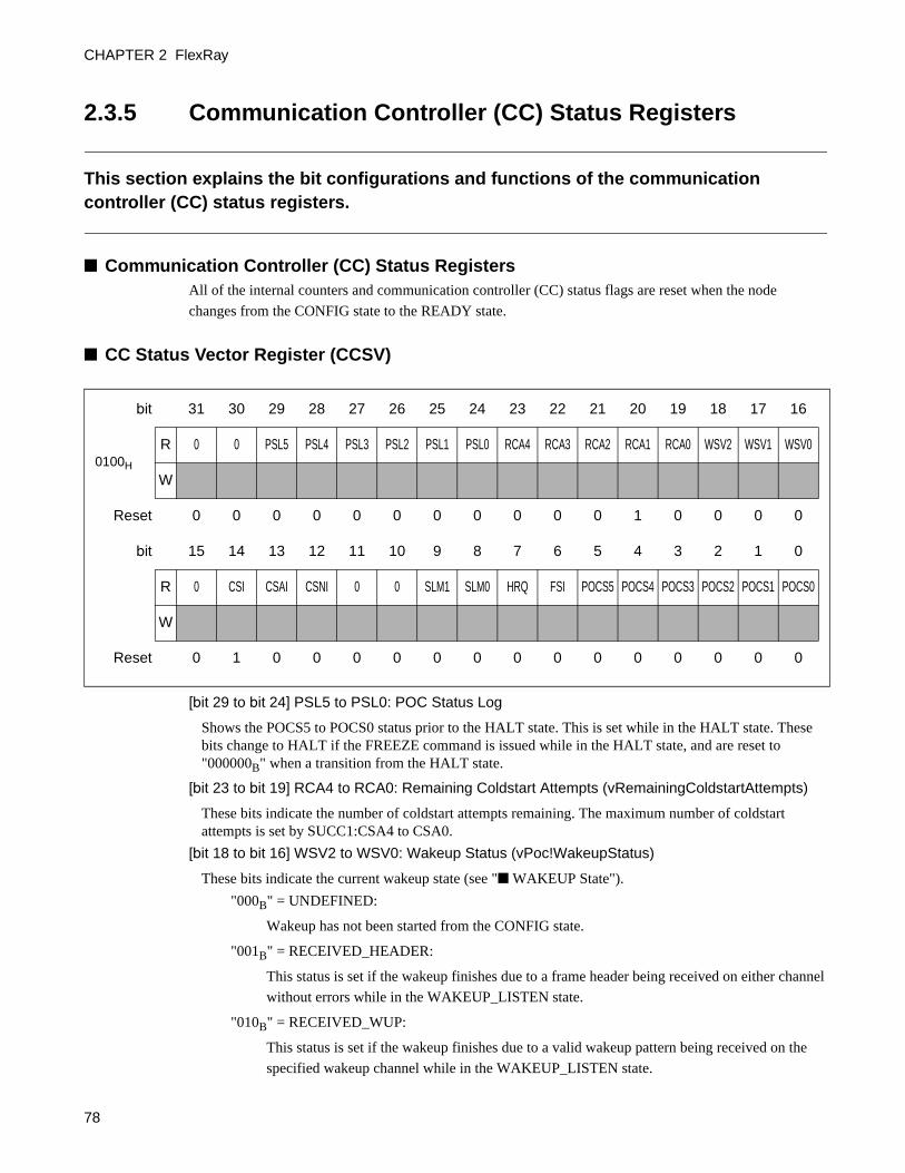
CHAPTER 2 FlexRay
2.3.5 Communication Controller (CC) Status Registers
This section explains the bit configurations and functions of the communication controller (CC) status registers.
■ Communication Controller (CC) Status RegistersAll of the internal counters and communication controller (CC) status flags are reset when the node
changes from the CONFIG state to the READY state.
■ CC Status Vector Register (CCSV)
[bit 29 to bit 24] PSL5 to PSL0: POC Status Log
Shows the POCS5 to POCS0 status prior to the HALT state. This is set while in the HALT state. These bits change to HALT if the FREEZE command is issued while in the HALT state, and are reset to "000000B" when a transition from the HALT state.
[bit 23 to bit 19] RCA4 to RCA0: Remaining Coldstart Attempts (vRemainingColdstartAttempts)
These bits indicate the number of coldstart attempts remaining. The maximum number of coldstart attempts is set by SUCC1:CSA4 to CSA0.
[bit 18 to bit 16] WSV2 to WSV0: Wakeup Status (vPoc!WakeupStatus)
These bits indicate the current wakeup state (see "■ WAKEUP State").
"000B" = UNDEFINED:
Wakeup has not been started from the CONFIG state.
"001B" = RECEIVED_HEADER:
This status is set if the wakeup finishes due to a frame header being received on either channel
without errors while in the WAKEUP_LISTEN state.
"010B" = RECEIVED_WUP:
This status is set if the wakeup finishes due to a valid wakeup pattern being received on the
specified wakeup channel while in the WAKEUP_LISTEN state.
bit 31 30 29 28 27 26 25 24 23 22 21 20 19 18 17 16
0100H
R 0 0 PSL5 PSL4 PSL3 PSL2 PSL1 PSL0 RCA4 RCA3 RCA2 RCA1 RCA0 WSV2 WSV1 WSV0
W
Reset 0 0 0 0 0 0 0 0 0 0 0 1 0 0 0 0
bit 15 14 13 12 11 10 9 8 7 6 5 4 3 2 1 0
R 0 CSI CSAI CSNI 0 0 SLM1 SLM0 HRQ FSI POCS5 POCS4 POCS3 POCS2 POCS1 POCS0
W
Reset 0 1 0 0 0 0 0 0 0 0 0 0 0 0 0 0
78

CHAPTER 2 FlexRay
"011B" = COLLISION_HEADER:
This status is set if the wakeup is aborted due to a collision being detected as a result of a valid
header being received on either channel while transmitting the wakeup pattern.
"100B" = COLLISION_WUP:
This status is set if the wakeup is aborted due to a collision being detected as a result of a valid
wakeup pattern being received on the specified channel while transmitting the wakeup pattern.
"101B" = COLLISION_UNKNOWN:
This status is set if there is a state transition from the WAKEUP_DETECT state and the wake
up is aborted due to the wakeup timer reaching the specified time without receiving a valid
wakeup pattern or a valid frame header.
"110B" = TRANSMITTED:
This status is set if the transmission of the wakeup pattern completes normally.
"111B" = reserved
[bit 14] CSI: Cold Start Inhibit (vColdstartInhibit)
Indicates that the node has been prohibited from performing coldstart. This flag is always set to "1" while in the READY state. This flag is reset by setting SUCC1:CMD3 to CMD0 to 1001B (CHI command ALLOW_COLDSTART).
"1" = Node coldstart prohibited
"0" = Node coldstart allowed
[bit 13] CSAI: Cold Start Abort Indicator
Indicates that the coldstart was aborted. This indicator is reset by setting CMD3 to CMD0 to 1010B (CHI command RESET_STATUS_INDICATORS).
[bit 12] CSNI: Cold Start Noise Indicator (vPoc!ColdstartNoise)
Indicates that the coldstart procedure executed under conditions where there was a lot of noise. This indicator is reset by setting CMD3 to CMD0 to 1010B (CHI command RESET_STATUS_INDICATORS).
[bit 9, bit 8] SLM1, SLM0: Slot Mode (vPoc!SlotMode)
Displays the current POC slot mode. The default value is the single slot mode, although this can be changed to all using SUCC1:TSM. If the CHI command CMD3 to CMD0 is set to 0101B (ALL_SLOTS) while in the NORMAL_ACTIVE or NORMAL_PASSIVE states, the node changes from the single slot mode to the all slot mode via ALL_PENDING mode. When the node is not in the NORMAL_ACTIVE or NORMAL_PASSIVE states, this changes to the value defined by SUCC1:TSM when CMD3 to CMD0 is set to 1010B (CHI command RESET_STATUS_INDICATORS).
"00B" = Single slot mode
"01B" = reserved
"10B" = ALL_PENDING
"11B" = All slot mode
[bit 7] HRQ: Halt Request (vPoc!CHIHaltRequest)
Indicates that a request has been made from the host for a state transition to the HALT state at the end of the communication cycle. This indicator is reset by setting CMD3 to CMD0 to 1010B (CHI command RESET_STATUS_INDICATORS), or when the node changes from the HALT state to the DEFAULT_CONFIG state or the READY state.
79

CHAPTER 2 FlexRay
[bit 6] FSI: Freeze Status Indicator (vPoc!Freeze)
Indicates that the node has changed to the HALT state due to CMD3 to CMD0 being set to 0111B (CHI command FREEZE), or an error occurring that required the node to change to the HALT state. This indicator is reset by setting CMD3 to CMD0 to 1010B (CHI command RESET_STATUS_INDICATORS), or when the node changes from the HALT state to the DEFAULT_CONFIG state.
[bit 5 to bit 0] POCS5 to POCS0: Protocol Operation Control Status
Displays the current POC execution state.
00 0000B = DEFAULT_CONFIG state
00 0001B = READY state
00 0010B = NORMAL_ACTIVE state
00 0011B = NORMAL_PASSIVE state
00 0100B = HALT state
00 0101B = MONITOR_MODE state
00 0110B to 00 1110B = reserved
00 1111B = CONFIG state
Displays the current POC status during the wakeup procedure.
01 0000B = WAKEUP_STANDBY state
01 0001B = WAKEUP_LISTEN state
01 0010B = WAKEUP_SEND state
01 0011B = WAKEUP_DETECT state
01 0100B to 01 1111B = reserved
Displays the current POC status during the startup procedure.
10 0000B = STARTUP_PREPARE state
10 0001B = COLDSTART_LISTEN state
10 0010B = COLDSTART_COLLISION_RESOLUTION state
10 0011B = COLDSTART_CONSISTENCY_CHECK state
10 0100B = COLDSTART_GAP state
10 0101B = COLDSTART_JOIN state
10 0110B = INTEGRATION_COLDSTART_CHECK state
10 0111B = INTEGRATION_LISTEN state
10 1000B = INTEGRATION_CONSISTENCY_CHECK state
10 1001B = INITIALIZE_SCHEDULE state
10 1010B = ABORT_STARTUP state
10 1011B to 11 1111B = reserved
Note:
Each of the flags CCSV:FSI, SUCC1:HRQ, CSNI, CSAI, SLM1, SLM0, and WSV2 to WSV0 is reset by setting CMD3 to CMD0 to 1010B (CHI command RESET_STATUS_INDICATORS).
80
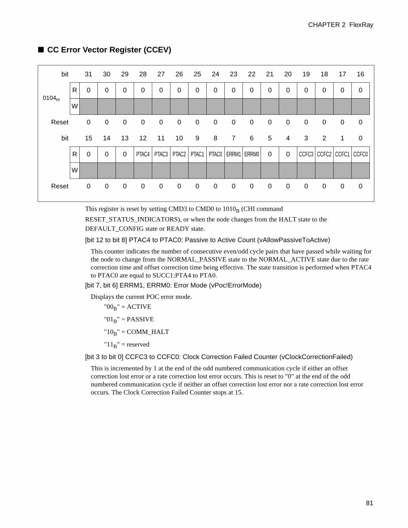
CHAPTER 2 FlexRay
■ CC Error Vector Register (CCEV)
This register is reset by setting CMD3 to CMD0 to 1010B (CHI command
RESET_STATUS_INDICATORS), or when the node changes from the HALT state to the
DEFAULT_CONFIG state or READY state.
[bit 12 to bit 8] PTAC4 to PTAC0: Passive to Active Count (vAllowPassiveToActive)
This counter indicates the number of consecutive even/odd cycle pairs that have passed while waiting for the node to change from the NORMAL_PASSIVE state to the NORMAL_ACTIVE state due to the rate correction time and offset correction time being effective. The state transition is performed when PTAC4 to PTAC0 are equal to SUCC1:PTA4 to PTA0.
[bit 7, bit 6] ERRM1, ERRM0: Error Mode (vPoc!ErrorMode)
Displays the current POC error mode.
"00B" = ACTIVE
"01B" = PASSIVE
"10B" = COMM_HALT
"11B" = reserved
[bit 3 to bit 0] CCFC3 to CCFC0: Clock Correction Failed Counter (vClockCorrectionFailed)
This is incremented by 1 at the end of the odd numbered communication cycle if either an offset correction lost error or a rate correction lost error occurs. This is reset to "0" at the end of the odd numbered communication cycle if neither an offset correction lost error nor a rate correction lost error occurs. The Clock Correction Failed Counter stops at 15.
bit 31 30 29 28 27 26 25 24 23 22 21 20 19 18 17 16
0104H
R 0 0 0 0 0 0 0 0 0 0 0 0 0 0 0 0
W
Reset 0 0 0 0 0 0 0 0 0 0 0 0 0 0 0 0
bit 15 14 13 12 11 10 9 8 7 6 5 4 3 2 1 0
R 0 0 0 PTAC4 PTAC3 PTAC2 PTAC1 PTAC0 ERRM1 ERRM0 0 0 CCFC3 CCFC2 CCFC1 CCFC0
W
Reset 0 0 0 0 0 0 0 0 0 0 0 0 0 0 0 0
81

CHAPTER 2 FlexRay
■ Slot Counter Value Register (SCV)
[bit 26 to bit 16] SCCB10 to SCCB0: Slot Counter Ch.B (vSlotCounter[B])
These bits show the current value of the ch.B slot counter. This value is set to "1" when the communication cycle starts, and is incremented at the end of each static slot until the end of the cycle. Valid values are in the range of 0 to 2047.
[bit 10 to bit 0] SCCA10 to SCCA0: Slot Counter Ch.A (vSlotCounter[A])
These bits show the current value of the ch.A slot counter. This value is set to "1" when the communication cycle starts, and is incremented at the end of each static slot until the end of the cycle. Valid values are in the range of 0 to 2047.
■ Macrotick and Cycle Counter Value Register (MTCCV)
[bit 21 to bit 16] CCV5 to CCV0: Cycle Counter Value (vCycleCounter)
These bits show the current value of the cycle counter. This value is incremented at the start of the communication cycle. Valid values are in the range of 0 to 63.
bit 31 30 29 28 27 26 25 24 23 22 21 20 19 18 17 16
0110H
R 0 0 0 0 0 SCCB10 SCCB9 SCCB8 SCCB7 SCCB6 SCCB5 SCCB4 SCCB3 SCCB2 SCCB1 SCCB0
W
Reset 0 0 0 0 0 0 0 0 0 0 0 0 0 0 0 0
bit 15 14 13 12 11 10 9 8 7 6 5 4 3 2 1 0
R 0 0 0 0 0 SCCA10 SCCA9 SCCA8 SCCA7 SCCA6 SCCA5 SCCA4 SCCA3 SCCA2 SCCA1 SCCA0
W
Reset 0 0 0 0 0 0 0 0 0 0 0 0 0 0 0 0
bit 31 30 29 28 27 26 25 24 23 22 21 20 19 18 17 16
0114H
R 0 0 0 0 0 0 0 0 0 0 CCV5 CCV4 CCV3 CCV2 CCV1 CCV0
W
Reset 0 0 0 0 0 0 0 0 0 0 0 0 0 0 0 0
bit 15 14 13 12 11 10 9 8 7 6 5 4 3 2 1 0
R 0 0 MTV13 MTV12 MTV11 MTV10 MTV9 MTV8 MTV7 MTV6 MTV5 MTV4 MTV3 MTV2 MTV1 MTV0
W
Reset 0 0 0 0 0 0 0 0 0 0 0 0 0 0 0 0
82

CHAPTER 2 FlexRay
[bit 13 to bit 0] MTV13 to MTV0: Macrotick Value (vMacrotick)
These bits show the current macrotick value. This value is set to "0" when the communication cycle starts, and is incremented until the end the cycle. Valid values are in the range of 0 to 16000.
■ Rate Correction Value Register (RCV)
[bit 11 to bit 0] RCV11 to RCV0: Rate Correction Value (vRateCorrection)
These bits show the rate correction (complement of 2). This is the rate correction value calculated internally by the controller before the maximum rate correction value GTUC10:MRC10 to MRC0 is applied. If this value exceeds the maximum rate correction value, the SFS:RCLR flag is set to "1".
■ Offset Correction Value Register (OCV)
[bit 18 to bit 0] OCV18 to OCV0:Offset Correction Value (vOffsetCorrection)
These bits show the offset correction (complement of 2). This is the offset correction value calculated internally by the controller before the maximum offset correction value GTUC10:MOC10 to MOC0 is applied. If this value exceeds the maximum offset correction value, the SFS:OCLR flag is set to "1".
bit 31 30 29 28 27 26 25 24 23 22 21 20 19 18 17 16
0118H
R 0 0 0 0 0 0 0 0 0 0 0 0 0 0 0 0
W
Reset 0 0 0 0 0 0 0 0 0 0 0 0 0 0 0 0
bit 15 14 13 12 11 10 9 8 7 6 5 4 3 2 1 0
R 0 0 0 0 RCV11 RCV10 RCV9 RCV8 RCV7 RCV6 RCV5 RCV4 RCV3 RCV2 RCV1 RCV0
W
Reset 0 0 0 0 0 0 0 0 0 0 0 0 0 0 0 0
bit 31 30 29 28 27 26 25 24 23 22 21 20 19 18 17 16
011CH
R 0 0 0 0 0 0 0 0 0 0 0 0 0 OCV18 OCV17 OCV16
W
Reset 0 0 0 0 0 0 0 0 0 0 0 0 0 0 0 0
bit 15 14 13 12 11 10 9 8 7 6 5 4 3 2 1 0
R OCV15 OCV14 OCV13 OCV12 OCV11 OCV10 OCV9 OCV8 OCV7 OCV6 OCV5 OCV4 OCV3 OCV2 OCV1 OCV0
W
Reset 0 0 0 0 0 0 0 0 0 0 0 0 0 0 0 0
83

CHAPTER 2 FlexRay
Note:
The external rate/offset correction values are added to the rate/offset correction values that are limited by the maximum rate/offset correction values.
■ Sync Frame Status Register (SFS)The maximum number of valid sync frames in one communication cycle is 15.
[bit 19] RCLR: Rate Correction Limit Reached
This flag indicates that the rate correction value has exceeded the limit value defined by GTUC10:MRC10 to MRC0. This flag is updated at the start of the offset correction phase.
"1" = The rate correction value has exceeded the limiting value
"0" = The rate correction value has not exceeded the limiting value
[bit 18] MRCS: Missing Rate Correction Signal
This flag indicates that no even/odd sync frame pairs were received and the rate correction calculation was not performed. This flag is updated at the start of the offset correction phase.
"1" = Rate correction signal missing
"0" = Rate correction signal valid
[bit 17] OCLR: Offset Correction Limit Reached
This flag indicates that the offset correction value has exceeded the limit value defined by GTUC10:MOC13 to MOC0. This flag is updated at the start of the offset correction phase.
"1" = The offset correction value has exceeded the limiting value
"0" = The offset correction value has not exceeded the limiting value
[bit 16] MOCS: Missing Offset Correction Signal
This flag indicates that no sync frames were received and the offset correction calculation was not performed. This flag is updated at the start of the offset correction phase.
"1" = Offset correction signal missing
"0" = Offset correction signal valid
bit 31 30 29 28 27 26 25 24 23 22 21 20 19 18 17 16
0120H
R 0 0 0 0 0 0 0 0 0 0 0 0 RCLR MRCS OCLR MOCS
W
Reset 0 0 0 0 0 0 0 0 0 0 0 0 0 0 0 0
bit 15 14 13 12 11 10 9 8 7 6 5 4 3 2 1 0
R VSBO3 VSBO2 VSBO1 VSBO0 VSBE3 VSBE2 VSBE1 VSBE0 VSAO3 VSAO2 VSAO1 VSAO0 VSAE3 VSAE2 VSAE1 VSAE0
W
Reset 0 0 0 0 0 0 0 0 0 0 0 0 0 0 0 0
84

CHAPTER 2 FlexRay
[bit 15 to bit 12] VSBO3 to VSBO0: Valid Sync Frames Ch.B, Odd Communication Cycle (vSyncFramesOddB)
These bits show the number of valid sync frames transmitted and received during odd numbered communication cycles on ch.B. This value is updated during the NIT period of each odd numbered communication cycle.
[bit 11 to bit 8] VSBE3 to VSBE0: Valid Sync Frames Ch.B, Even Communication Cycle (vSyncFramesEvenB)
These bits show the number of valid sync frames transmitted and received during even numbered communication cycles on ch.B. This value is updated during the NIT period of each even numbered communication cycle.
[bit 7 to bit 4] VSAO3 to VSAO0: Valid Sync Frames Ch.A, Odd Communication Cycle (vSyncFramesOddA)
These bits show the number of valid sync frames transmitted and received during odd numbered communication cycles on ch.A. This value is updated during the NIT period of each odd numbered communication cycle.
[bit 3 to bit 0] VSAE3 to VSAE0: Valid Sync Frames Ch.A, Even Communication Cycle (vSyncFramesEvenA)
These bits show the number of valid sync frames transmitted and received during even numbered communication cycles on ch.A. This value is updated during the NIT period of each even numbered communication cycle.
Note:
Bit15 to bit0 are only valid if each of the channels is allocated by SUCC1:CCHA or CCHB.
■ Symbol Window and NIT Status Register (SWNIT)
The followings describe the bits that hold status information related to the NIT. These bits are updated at
the end of the NIT of each channel.
[bit 11] SBNB: Slot Boundary Violation During NIT Ch.B (vSS!BViolationB)
"1" = A slot boundary violation was detected during the NIT on ch.B
"0" = No slot boundary violations were detected during the NIT on ch.B
bit 31 30 29 28 27 26 25 24 23 22 21 20 19 18 17 16
0124H
R 0 0 0 0 0 0 0 0 0 0 0 0 0 0 0 0
W
Reset 0 0 0 0 0 0 0 0 0 0 0 0 0 0 0 0
bit 15 14 13 12 11 10 9 8 7 6 5 4 3 2 1 0
R 0 0 0 0 SBNB SENB SBNA SENA MTSB MTSA TCSB SBSB SESB TCSA SBSA SESA
W
Reset 0 0 0 0 0 0 0 0 0 0 0 0 0 0 0 0
85

CHAPTER 2 FlexRay
[bit 10] SENB: Syntax Error During NIT Ch.B (vSS!SyntaxErrorB)
"1" = A syntax error was detected during the NIT on ch.B
"0" = No syntax errors were detected during the NIT on ch.B
[bit 9] SBNA: Slot Boundary Violation During NIT Ch.A (vSS!BViolationA)
"1" = A slot boundary violation was detected during the NIT on ch.A
"0" = No slot boundary violations were detected during the NIT on ch.A
[bit 8] SENA: Syntax Error During NIT Ch.A (vSS!SyntaxErrorA)
"1" = A syntax error was detected during the NIT on ch.A
"0" = No syntax errors were detected during the NIT on ch.A
The followings describe the bits that hold status information related to the symbol window. These bits are
updated at the end of the symbol window of each channel. These are not updated during startup.
[bit 7] MTSB: MTS Received on Ch.B (vSS!ValidMTSB)
"1" = An MTS symbol was detected on ch.B
"0" = No MTS symbols were detected on ch.B
[bit 6] MTSA: MTS Received on Ch.A (vSS!ValidMTSA)
"1" = An MTS symbol was detected on ch.A
"0" = No MTS symbols were detected on ch.A
[bit 5] TCSB: Transmission Collision in Symbol Window Ch.B (vSS!TxConflictB)
"1" = A transmission collision was detected in ch.B symbol window
"0" = No transmission collisions were detected in ch.B symbol window
[bit 4] SBSB: Slot Boundary Violation in Symbol Window Ch.B (vSS!BViolationB)
"1" = A slot boundary violation was detected in ch.B symbol window
"0" = No slot boundary violations were detected in ch.B symbol window
[bit 3] SESB: Syntax Error in Symbol Window Ch.B (vSS!SyntaxErrorB)
"1" = A syntax error was detected in ch.B symbol window
"0" = No syntax errors were detected in ch.B symbol window
[bit 2] TCSA: Transmission Collision in Symbol Window Ch.A (vSS!TxConflictA)
"1" = A transmission collision was detected in ch.A symbol window
"0" = No transmission collisions were detected in ch.A symbol window
[bit 1] SBSA: Slot Boundary Violation in Symbol Window Ch.A (vSS!BViolationA)
"1" = A slot boundary violation was detected in ch.A symbol window
"0" = No slot boundary violations were detected in ch.A symbol window
[bit 0] SESA: Syntax Error in Symbol Window Ch.A (vSS!SyntaxErrorA)
"1" = A syntax error was detected in ch.A symbol window
"0" = No syntax errors were detected in ch.A symbol window
86

CHAPTER 2 FlexRay
■ Aggregated Channel Status (ACS)This register provides the status that occurs during the operation of all of the communication slot channels
regardless of whether the communication slots are allocated for transmission or reception. This register also
contains the status data from the symbol window and NIT. This status data is updated after each slot (the
latest data at the end of the next slot).
Each of the flags in this register is cleared by writing "1" to the corresponding bit position. Writing "0" has
no effect on these flags. All of the flags are cleared by a hardware reset.
[bit 12] SBVB: Slot Boundary Violation on Ch.B (vSS!BViolationB)
This bit indicates that at least one slot boundary violation has been observed between the static slot, dynamic slot, symbol window, or NIT on ch.B.
"1" = A slot boundary violation has been observed on ch.B
"0" = No slot boundary violations have been observed on ch.B
[bit 11] CIB: Communication Indicator Ch.B
This bit indicates that at least one valid frame has been received in a slot that contained an additional communication on ch.B. In other words, this means that a valid frame has been received in at least one slot, and this was combined with either a syntax error, a contents error, or a slot boundary violation.
"1" = A frame containing an additional communication has been received on ch.B
"0" = No frames containing additional communications have been received on ch.B
[bit 10] CEDB: Content Error Detected on Ch.B (vSS!ContentErrorB)
This bit indicates that at least one frame containing a content error has been received in a static slot or dynamic slot of ch.B.
"1" = A frame containing a content error has been received on ch.B
"0" = No frames containing content errors have been received on ch.B
[bit 9] SEDB: Syntax Error Detected on Ch.B (vSS!SyntaxErrorB)
This bit indicates that at least one syntax error has been observed in a static slot, dynamic slot, symbol window, or NIT on ch.B.
"1" = A syntax error has been observed on ch.B
"0" = No syntax errors have been observed on ch.B
bit 31 30 29 28 27 26 25 24 23 22 21 20 19 18 17 16
0128H
R 0 0 0 0 0 0 0 0 0 0 0 0 0 0 0 0
W
Reset 0 0 0 0 0 0 0 0 0 0 0 0 0 0 0 0
bit 15 14 13 12 11 10 9 8 7 6 5 4 3 2 1 0
R 0 0 0SBVB CIB CEDB SEDB VFRB
0 0 0SBVA CIA CEDA SEDA VFRA
W
Reset 0 0 0 0 0 0 0 0 0 0 0 0 0 0 0 0
87

CHAPTER 2 FlexRay
[bit 8] VFRB: Valid Frame Received on Ch.B (vSS!ValidFrameB)
This bit indicates that at least one valid frame has been received in a static slot or dynamic slot of ch.B.
"1" = A valid frame has been received on ch.B
"0" = No valid frames have been received on ch.B
[bit 4] SBVA: Slot Boundary Violation on Ch.A (vSS!BViolationA)
This bit indicates that at least one slot boundary violation has been observed between the static slot, dynamic slot, symbol window, or NIT on ch.A.
"1" = A slot boundary violation has been observed on ch.A
"0" = No slot boundary violations have been observed on ch.A
[bit 3] CIA: Communication Indicator Ch.A
This bit indicates that at least one valid frame has been received in a slot that contained an additional communication on ch.A. In other words, this means that a valid frame has been received in at least one slot, and this was combined with either a syntax error, a contents error, or a slot boundary violation.
"1" = A frame containing an additional communication has been received on ch.A
"0" = No frames containing additional communications have been received on ch.A
[bit 2] CEDA: Content Error Detected on Ch.A (vSS!ContentErrorA)
This bit indicates that at least one frame containing a content error has been received in a static slot or dynamic slot of ch.A.
"1" = A frame containing a content error has been received on ch.A
"0" = No frames containing content errors have been received on ch.A
[bit 1] SEDA: Syntax Error Detected on Ch.A (vSS!SyntaxErrorA)
This bit indicates that at least one syntax error has been observed in a static slot, dynamic slot, symbol window, or NIT on ch.A.
"1" = A syntax error has been observed on ch.A
"0" = No syntax errors have been observed on ch.A
[bit 0] VFRA: Valid Frame Received on Ch.A (vSS!ValidFrameA)
This bit indicates that at least one valid frame has been received in a static slot or dynamic slot of ch.A.
"1" = A valid frame has been received on ch.A
"0" = No valid frames have been received on ch.A
Note:
When any of the SEDB, CIB, CEDB, or SBVB flags change from "0" to "1", the interrupt flag EIR:EDB is set to "1". When any of the SEDA, CEDA, CIA, or SBVA flags change from "0" to "1", the interrupt flag EIR:EDA is set to "1".
88

CHAPTER 2 FlexRay
■ Even Numbered Cycle Sync Frame ID Register (ESID1 to ESID15)The 15 registers ESID1 to ESID15 store in ascending order the frame IDs of sync frames received during
the even numbered communication cycles. The smallest sync frame ID received is therefore stored in
ESID1 register. If the node transmits a sync frame during the even numbered communication cycle, the
frame ID of the transmitted sync frame is stored in ESID1 register. The value of these registers is updated
during the NIT of each even numbered communication cycle.
[bit 15] RXEB: Received Even Numbered Sync ID on Ch.B
This bit indicates that a sync frame corresponding to the sync ID was received on ch.B during the even cycle.
"1" = A sync frame was received on ch.B
"0" = No sync frames were received on ch.B
[bit 14] RXEA: Received Even Numbered Sync ID on Ch.A
This bit indicates that a sync frame corresponding to the sync ID was received on ch.A during the even numbered cycle.
"1" = A sync frame was received on ch.A
"0" = No sync frames were received on ch.A
[bit 9 to bit 0] EID9 to EID0: Even Sync ID (vsSyncIDListA,Beven)
These bits show the sync frame ID of the even numbered communication cycle.
bit 31 30 29 28 27 26 25 24 23 22 21 20 19 18 17 16
0130H to 0168H
R 0 0 0 0 0 0 0 0 0 0 0 0 0 0 0 0
W
Reset 0 0 0 0 0 0 0 0 0 0 0 0 0 0 0 0
bit 15 14 13 12 11 10 9 8 7 6 5 4 3 2 1 0
R RXEB RXEA 0 0 0 0 EID9 EID8 EID7 EID6 EID5 EID4 EID3 EID2 EID1 EID0
W
Reset 0 0 0 0 0 0 0 0 0 0 0 0 0 0 0 0
89
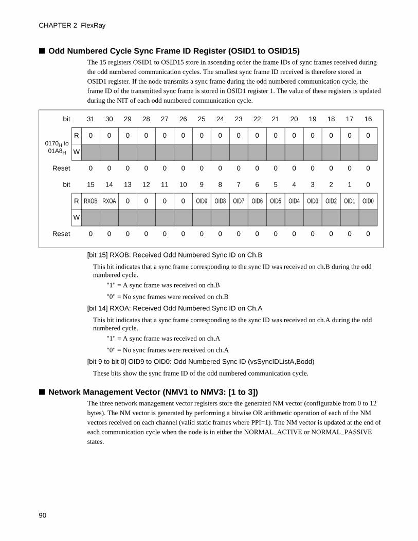
CHAPTER 2 FlexRay
■ Odd Numbered Cycle Sync Frame ID Register (OSID1 to OSID15)The 15 registers OSID1 to OSID15 store in ascending order the frame IDs of sync frames received during
the odd numbered communication cycles. The smallest sync frame ID received is therefore stored in
OSID1 register. If the node transmits a sync frame during the odd numbered communication cycle, the
frame ID of the transmitted sync frame is stored in OSID1 register 1. The value of these registers is updated
during the NIT of each odd numbered communication cycle.
[bit 15] RXOB: Received Odd Numbered Sync ID on Ch.B
This bit indicates that a sync frame corresponding to the sync ID was received on ch.B during the odd numbered cycle.
"1" = A sync frame was received on ch.B
"0" = No sync frames were received on ch.B
[bit 14] RXOA: Received Odd Numbered Sync ID on Ch.A
This bit indicates that a sync frame corresponding to the sync ID was received on ch.A during the odd numbered cycle.
"1" = A sync frame was received on ch.A
"0" = No sync frames were received on ch.A
[bit 9 to bit 0] OID9 to OID0: Odd Numbered Sync ID (vsSyncIDListA,Bodd)
These bits show the sync frame ID of the odd numbered communication cycle.
■ Network Management Vector (NMV1 to NMV3: [1 to 3])The three network management vector registers store the generated NM vector (configurable from 0 to 12
bytes). The NM vector is generated by performing a bitwise OR arithmetic operation of each of the NM
vectors received on each channel (valid static frames where PPI=1). The NM vector is updated at the end of
each communication cycle when the node is in either the NORMAL_ACTIVE or NORMAL_PASSIVE
states.
bit 31 30 29 28 27 26 25 24 23 22 21 20 19 18 17 16
0170H to 01A8H
R 0 0 0 0 0 0 0 0 0 0 0 0 0 0 0 0
W
Reset 0 0 0 0 0 0 0 0 0 0 0 0 0 0 0 0
bit 15 14 13 12 11 10 9 8 7 6 5 4 3 2 1 0
R RXOB RXOA 0 0 0 0 OID9 OID8 OID7 OID6 OID5 OID4 OID3 OID2 OID1 OID0
W
Reset 0 0 0 0 0 0 0 0 0 0 0 0 0 0 0 0
90

CHAPTER 2 FlexRay
The NMVn registers beyond the configured length of the NM vector are not valid.
Figure 2.3-7 below shows the allocation of the byte data in the network management vector.
Figure 2.3-7 Allocation of Byte Data in the Network Management Vector
bit 31 30 29 28 27 26 25 24 23 22 21 20 19 18 17 16
01B0H to 01B8H
R NM 31 NM 30 NM 29 NM 28 NM 27 NM 26 NM 25 NM 24 NM 23 NM 22 NM 21 NM 20 NM 19 NM 18 NM 17 NM 16
W
Reset 0 0 0 0 0 0 0 0 0 0 0 0 0 0 0 0
bit 15 14 13 12 11 10 9 8 7 6 5 4 3 2 1 0
R NM 15 NM 14 NM 13 NM 12 NM 11 NM 10 NM 9 NM8 NM7 NM6 NM5 NM4 NM3 NM2 NM1 NM0
W
Reset 0 0 0 0 0 0 0 0 0 0 0 0 0 0 0 0
bit
Word31 30 29 28 27 26 25 24 23 22 21 20 19 18 17 16 15 14 13 12 11 10 9 8 7 6 5 4 3 2 1 0
NMV1 Data3 Data2 Data1 Data0
NMV2 Data7 Data6 Data5 Data4
NMV3 Data11 Data10 Data9 Data8
91

CHAPTER 2 FlexRay
2.3.6 Message Buffer Control Register
This section explains the bit configurations and functions of the message buffer control register.
■ Message RAM Configuration Register (MRC)The Message RAM Configuration Register defines the message buffers that are allocated to the static segment,
dynamic segment, and FIFO. This register can only be written to while in the DEFAULT_CONFIG or CONFIG
states.
[bit 26] SPLM: Sync Frame Payload Multiplex
This bit is valid when the node is configured as a sync node (SUCC1:TXSY=1). When this bit is set to "1", message buffer 0 and 1 are dedicated to transmitting sync frames with different payload data on ch.A and ch.B. When this bit is set to "0", the sync frames contain the same payload data on both channels, and are transmitted from message buffer 0. Note that message buffer 1 must be selected according to the channel filter settings for message buffer 0.
"0" = Both message buffer 0 1 are locked against reconfiguration
"1" = Message buffer 0 is locked against reconfiguration
[bit 25, bit 24] SEC1, SEC0: Secure Buffers
These bits are ignored in the DEFAULT_CONFIG and CONFIG states.
"00B" = The message buffers can be reconfigured
"01B" = Message buffers with a number smaller than FDB are locked from
reconfiguration, and message buffers configured for the static segment that have a buffer
number greater than or equal to FDB are unable to transmit.
"10B" = All of the message buffers are locked against reconfiguration
"11B" = All of the message buffers are locked against reconfiguration
Furthermore, message buffers that are configured for the static segment and that have a
buffer number greater than or equal to FDB are unable to transmit
bit 31 30 29 28 27 26 25 24 23 22 21 20 19 18 17 16
0300H
R 0 0 0 0 0SPLM* SEC1* SEC0* LCB7* LCB6* LCB5* LCB4* LCB3* LCB2* LCB1* LCB0*
W
Reset 0 0 0 0 0 0 0 1 1 0 0 0 0 0 0 0
bit 15 14 13 12 11 10 9 8 7 6 5 4 3 2 1 0
RFFB7* FFB6* FFB5* FFB4* FFB3* FFB2* FFB1* FFB0* FDB7* FDB6* FDB5* FDB4* FDB3* FDB2* FDB1* FDB0*
W
Reset 0 0 0 0 0 0 0 0 0 0 0 0 0 0 0 0
92

CHAPTER 2 FlexRay
[bit 23 to bit 16] LCB7 to LCB0: Last Configured Buffer
0 to 127 = The number of message buffers is (LCB + 1)
1 to 127 = LCB message buffers from FFB are allocated to the FIFO area
128 to 255 = There are no message buffers configured
[bit 15 to bit 8] FFB7 to FFB0: First Buffer of FIFO
0 = All of the message buffers are allocated to the FIFO area
1 to 127 = FFB1 message buffer from 0 are allocated to the static segment area
128 to 255 = There are no message buffers allocated to the FIFO area
[bit 7 to bit 0] FDB7 to FDB0: First Dynamic Buffer
0 = There is no group of buffers that are configured exclusively for the static segment
128 to 255 = There are no buffers configured for the dynamic segment
Note:
If the node is configured as a sync node (SUCC1:TXSY=1), message buffer 0 and 1 are both used as sync frames and then need to be configured using the key slot ID of the node specifications. If the node is not configured as a sync node (SUCC1:TXSY=0), message buffer 0 and 1 are both handled the same as other message buffers.
Verify that FDB7 to FDB0, FFB7 to FFB0, and LCB7 to LCB0 are configured correctly. Operation is not guaranteed if these parameters are not configured correctly. The CC does not check for incorrect configurations.
The maximum number of header sections is 128. This means that a maximum of 128 message buffers can be configured. The maximum length of a single data section is 254 bytes. The length of the data section can be configured differently for each message buffer. See "2.7.12 Message RAM" for details.
Set the data section lengths and payloads of all of the message buffers that belong to the FIFO using WRHS2:PLC6 to PLC0 and WRHS3:DP10 to DP0 to the same values.
The message buffers that belong to the FIFO are locked against reconfiguration when the CC is not in the DEFAULT_CONFIG or CONFIG states.
Message Buffer 0
Message Buffer 1
Message Buffer N
Message Buffer N-1
Static Buffers
Static + DynamicBuffers...
FDB
FIFO configured: FFB > FDB
CLB > FDB, LVB > FFB
No FIFO configured: FFB > 128FFB
LCB
FIFO
93

CHAPTER 2 FlexRay
■ FIFO Rejection Filter Register (FRF)The FIFO Rejection Filter Register configures bit strings that are compared against the channel, frame ID,
and cycle count of received frames. This register is used in conjunction with the FIFO Rejection Filter
Mask Register to determine whether or not to reject messages from the FIFO. This register can only be
written to while in the DEFAULT_CONFIG or CONFIG states.
[bit 24] RNF: Reject Null Frames
When this bit is set to "1", null frames that are received are not stored in the FIFO.
"1" = Null frames are not stored in the FIFO
"0" = Null frames are stored in the FIFO
[bit 23] RSS: Reject Messages in Static Segment
When this bit is set to "1", the FIFO only receives messages from the dynamic segment.
"1" = Messages are not received from the static segment
"0" = Messages are received from the static segment and the dynamic segment
[bit 22 to bit 16] CYF6 to CYF0: Cycle Code Filter
This 7-bit cycle counter filter specifies the cycle set and determines the communication cycle to which the frame ID filter and channel filter are applied. No frames are received during cycles where the frame ID filter and channel filter are not applied due to the cycle set specified by this register. See "■ Cycle Counter Filtering" for details on configuring the cycle counter filter.
[bit 12 to bit 2] FID10 to FID0: Frame ID Filter
If the value of this filter is set to a frame ID of "0", the FIFO will receive all frame IDs.
0 to 2047 = Frame ID filter value
[bit 1, bit 0] CH1, CH0: Channel Filter
"11B" = Unable to receive
"10B" = Only receive on ch.A
"01B" = Only receive on ch.B
"00B" = Receive on both channels
bit 31 30 29 28 27 26 25 24 23 22 21 20 19 18 17 16
0304H
R 0 0 0 0 0 0 0RNF* RSS* CYF6* CYF5* CYF4* CYF3* CYF2* CYF1* CYF0*
W
Reset 0 0 0 0 0 0 0 1 1 0 0 0 0 0 0 0
bit 15 14 13 12 11 10 9 8 7 6 5 4 3 2 1 0
R 0 0 0FID 10* FID 9* FID 8* FID 7* FID 6* FID 5* FID 4* FID 3* FID 2* FID 1* FID 0* CH1* CH0*
W
Reset 0 0 0 0 0 0 0 0 0 0 0 0 0 0 0 0
94
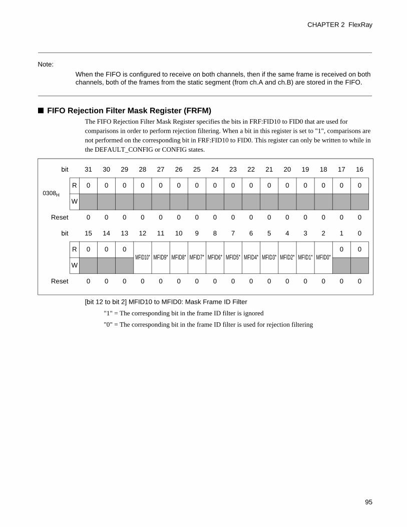
CHAPTER 2 FlexRay
Note:
When the FIFO is configured to receive on both channels, then if the same frame is received on both channels, both of the frames from the static segment (from ch.A and ch.B) are stored in the FIFO.
■ FIFO Rejection Filter Mask Register (FRFM)The FIFO Rejection Filter Mask Register specifies the bits in FRF:FID10 to FID0 that are used for
comparisons in order to perform rejection filtering. When a bit in this register is set to "1", comparisons are
not performed on the corresponding bit in FRF:FID10 to FID0. This register can only be written to while in
the DEFAULT_CONFIG or CONFIG states.
[bit 12 to bit 2] MFID10 to MFID0: Mask Frame ID Filter
"1" = The corresponding bit in the frame ID filter is ignored
"0" = The corresponding bit in the frame ID filter is used for rejection filtering
bit 31 30 29 28 27 26 25 24 23 22 21 20 19 18 17 16
0308H
R 0 0 0 0 0 0 0 0 0 0 0 0 0 0 0 0
W
Reset 0 0 0 0 0 0 0 0 0 0 0 0 0 0 0 0
bit 15 14 13 12 11 10 9 8 7 6 5 4 3 2 1 0
R 0 0 0MFID10* MFID9* MFID8* MFID7* MFID6* MFID5* MFID4* MFID3* MFID2* MFID1* MFID0*
0 0
W
Reset 0 0 0 0 0 0 0 0 0 0 0 0 0 0 0 0
95
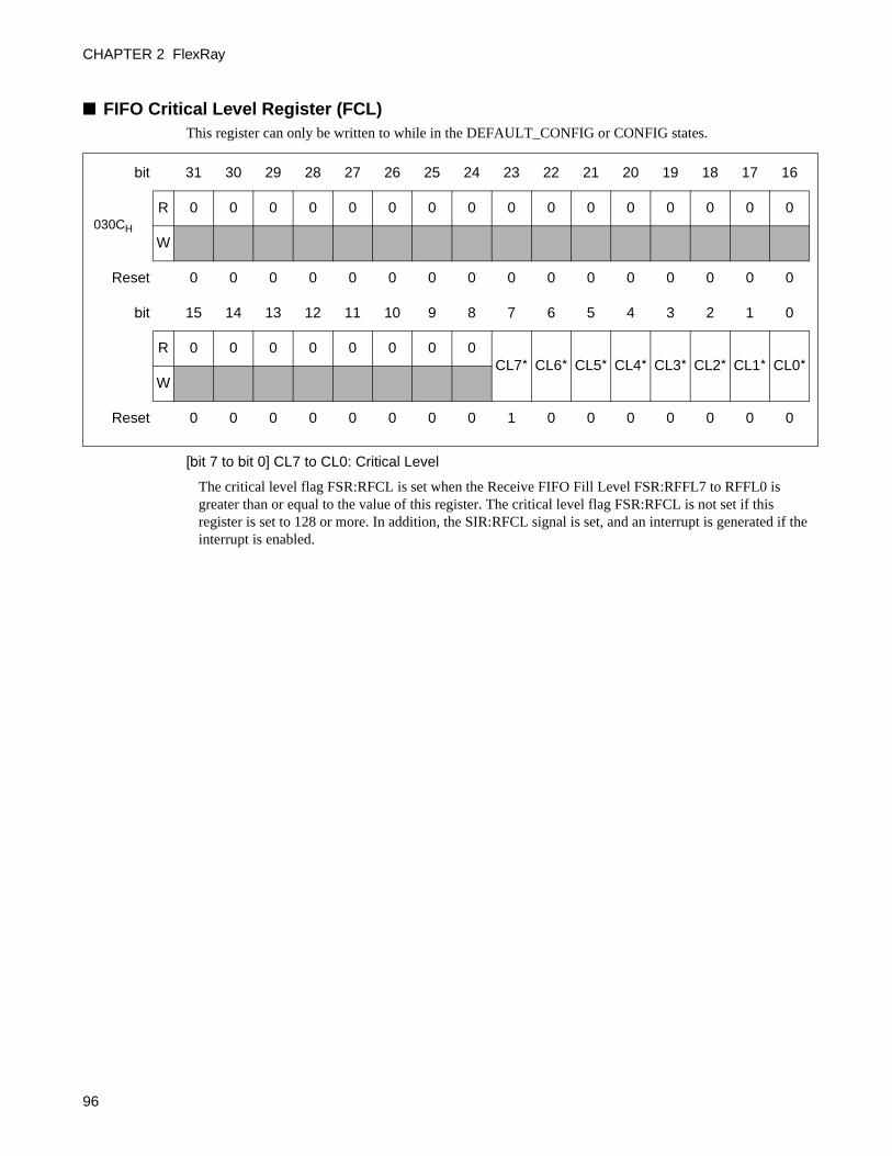
CHAPTER 2 FlexRay
■ FIFO Critical Level Register (FCL)This register can only be written to while in the DEFAULT_CONFIG or CONFIG states.
[bit 7 to bit 0] CL7 to CL0: Critical Level
The critical level flag FSR:RFCL is set when the Receive FIFO Fill Level FSR:RFFL7 to RFFL0 is greater than or equal to the value of this register. The critical level flag FSR:RFCL is not set if this register is set to 128 or more. In addition, the SIR:RFCL signal is set, and an interrupt is generated if the interrupt is enabled.
bit 31 30 29 28 27 26 25 24 23 22 21 20 19 18 17 16
030CH
R 0 0 0 0 0 0 0 0 0 0 0 0 0 0 0 0
W
Reset 0 0 0 0 0 0 0 0 0 0 0 0 0 0 0 0
bit 15 14 13 12 11 10 9 8 7 6 5 4 3 2 1 0
R 0 0 0 0 0 0 0 0CL7* CL6* CL5* CL4* CL3* CL2* CL1* CL0*
W
Reset 0 0 0 0 0 0 0 0 1 0 0 0 0 0 0 0
96

CHAPTER 2 FlexRay
2.3.7 Message Buffer Status Register
This section explains the bit configurations and functions of the message buffer status register.
■ Message Handler Status Register (MHDS)
The bits in this register that are writable can be cleared by writing "1". Writing "0" has no effect on these
bits. This register is cleared by a hardware reset.
[bit 30 to bit 24] MBU6 to MBU0: Message Buffer Updated
These bits show the number of the last message buffer that was updated. The ND127 to ND0 and MBS127 to MBS0 flags in the NDAT1, NDAT2, NDAT3, NDAT4, MBSC1, MBSC2, MBSC3, and MBSC4 registers that correspond to this message buffer are also updated.
[bit 22 to bit 16] MBT6 to MBT0: Message Buffer Transmitted
These bits show the number of the last message buffer that was transmitted correctly. If the message buffer is set to single shot mode, the TXR127 to TXR0 flags in the TXRQ1, TXRQ2, TXRQ3, and TXRQ4 registers are reset.
Note:
The MBT6 to MBT0 and MBU6 to MBU0 flags are reset when the node changes from the CONFIG state or changes to the STARTUP state.
[bit 14 to bit 8] FMB6 to FMB0: Faulty Message Buffer
These bits show the message buffer number if a parity error occurs in the following situations.
- When reading the message buffer
- While transferring data from the input buffer or transient buffer 1 or 2 to a message buffer
This value is only valid when one of the PIBF, PMR, PTBF1, PTBF2, or FMBD flags is set to "1". This flag is updated after the FMBD flag is reset.
bit 31 30 29 28 27 26 25 24 23 22 21 20 19 18 17 16
0310H
R 0 MBU6 MBU5 MBU4 MBU3 MBU2 MBU1 MBU0 0 MBT6 MBT5 MBT4 MBT3 MBT2 MBT1 MBT0
W
Reset 0 0 0 0 0 0 0 0 0 0 0 0 0 0 0 0
bit 15 14 13 12 11 10 9 8 7 6 5 4 3 2 1 0
R 0 FMB6 FMB5 FMB4 FMB3 FMB2 FMB1 FMB0 CRAMMFMB FMBD PTBF2 PTBF1 PMR POBF PIBF
W
Reset 0 0 0 0 0 0 0 0 0 0 0 0 0 0 0 0
97

CHAPTER 2 FlexRay
[bit 7] CRAM: Clear All Internal RAM
This flag indicates whether the CHI command CLEAR_RAMS (CMD3 to CMD0 = 1100B) is currently executing (all of the bits in all of the internal RAM blocks are being written to "0"). This bit is set to "1" by a hardware reset or by the CHI command CLEAR_RAMS.
"1" = The CHI command CLEAR_RAMS is currently executing
"0" = The CHI command CLEAR_RAMS is not currently executing
[bit 6] MFMB:Multiple Faulty Message Buffers Detected
"1" = Another faulty message buffer was detected while the FMBD flag was set
"0" = Another faulty message buffer has not been found
[bit 5] FMBD: Faulty Message Buffer Detected
"1" = The message buffer pointed to by FMB6 to FMB0 has a failure error due to a parity error
"0" = There are no faulty message buffers
[bit 4] PTBF2: Parity Error Transient Buffer RAM B
"1" = A parity error occurred when reading from transient buffer RAM B
"0" = A parity error has not occurred
[bit 3] PTBF1: Parity Error Transient Buffer RAM A
"1" = A parity error occurred when reading transient buffer RAM A
"0" = A parity error has not occurred
[bit 2] PMR: Parity Error Message RAM
"1" = A parity error occurred when reading message RAM
"0" = A parity error has not occurred
[bit 1] POBF: Parity Error Output Buffer RAM 1, 2
"1" = A parity error occurred when reading output buffer RAM 1, 2
"0" = A parity error has not occurred
[bit 0] PIBF: Parity Error Input Buffer RAM 1, 2
"1" = A parity error occurred when reading input buffer RAM 1, 2
"0" = A parity error has not occurred
Note:
When any of the PIBF, POBF, PMR, PTBF1, or PTBF2 bits changes from "0" to "1", EIR:PERR is set to "1".
98
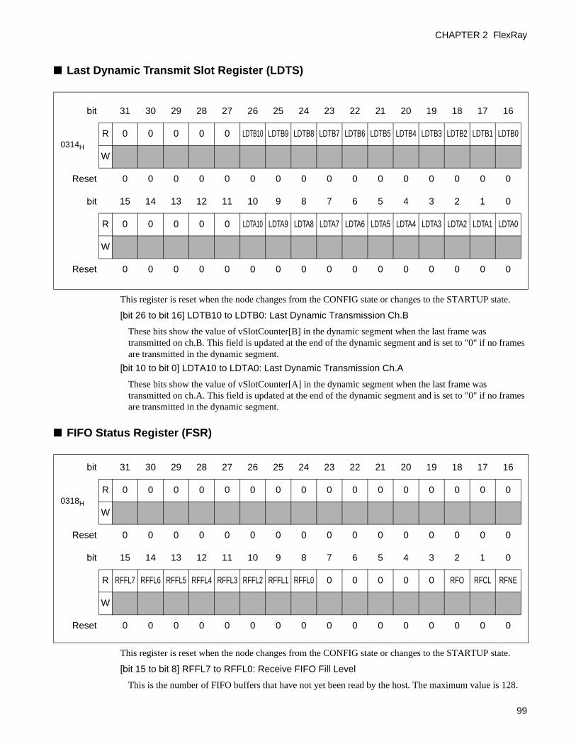
CHAPTER 2 FlexRay
■ Last Dynamic Transmit Slot Register (LDTS)
This register is reset when the node changes from the CONFIG state or changes to the STARTUP state.
[bit 26 to bit 16] LDTB10 to LDTB0: Last Dynamic Transmission Ch.B
These bits show the value of vSlotCounter[B] in the dynamic segment when the last frame was transmitted on ch.B. This field is updated at the end of the dynamic segment and is set to "0" if no frames are transmitted in the dynamic segment.
[bit 10 to bit 0] LDTA10 to LDTA0: Last Dynamic Transmission Ch.A
These bits show the value of vSlotCounter[A] in the dynamic segment when the last frame was transmitted on ch.A. This field is updated at the end of the dynamic segment and is set to "0" if no frames are transmitted in the dynamic segment.
■ FIFO Status Register (FSR)
This register is reset when the node changes from the CONFIG state or changes to the STARTUP state.
[bit 15 to bit 8] RFFL7 to RFFL0: Receive FIFO Fill Level
This is the number of FIFO buffers that have not yet been read by the host. The maximum value is 128.
bit 31 30 29 28 27 26 25 24 23 22 21 20 19 18 17 16
0314H
R 0 0 0 0 0 LDTB10 LDTB9 LDTB8 LDTB7 LDTB6 LDTB5 LDTB4 LDTB3 LDTB2 LDTB1 LDTB0
W
Reset 0 0 0 0 0 0 0 0 0 0 0 0 0 0 0 0
bit 15 14 13 12 11 10 9 8 7 6 5 4 3 2 1 0
R 0 0 0 0 0 LDTA10 LDTA9 LDTA8 LDTA7 LDTA6 LDTA5 LDTA4 LDTA3 LDTA2 LDTA1 LDTA0
W
Reset 0 0 0 0 0 0 0 0 0 0 0 0 0 0 0 0
bit 31 30 29 28 27 26 25 24 23 22 21 20 19 18 17 16
0318H
R 0 0 0 0 0 0 0 0 0 0 0 0 0 0 0 0
W
Reset 0 0 0 0 0 0 0 0 0 0 0 0 0 0 0 0
bit 15 14 13 12 11 10 9 8 7 6 5 4 3 2 1 0
R RFFL7 RFFL6 RFFL5 RFFL4 RFFL3 RFFL2 RFFL1 RFFL0 0 0 0 0 0 RFO RFCL RFNE
W
Reset 0 0 0 0 0 0 0 0 0 0 0 0 0 0 0 0
99

CHAPTER 2 FlexRay
[bit 2] RFO: Receive FIFO Overrun
This flag is set if a receive FIFO overrun is detected. When an overrun occurs, the oldest messages are overwritten. The interrupt flag (EIR:RFO) is also set. The flag is cleared by read access to the FIFO.
"1" = The receive FIFO is overrun
"0" = The receive FIFO is not overrun
[bit 1] RFCL: Receive FIFO Critical Level
This flag is set when the receive FIFO fill level (RFFL7 to RFFL0) is greater than or equal to the configured critical level (FCL:CL7 to CL0). Furthermore, the flag is cleared immediately if the fill level drops below the critical level. If RFCL is changed from "0" to "1", then SIR:RFCL is set to "1" and an interrupt is generated if the interrupt is enabled.
"1" = The receive FIFO has reached the critical level
"0" = The receive FIFO is below the critical level
[bit 0] RFNE: Receive FIFO Not Empty
This bit is set when a valid frame (or a null frame depending on the data and rejection masks) is received and stored in the FIFO. The interrupt flag (SIR:RFNE) is also set. The host resets this bit after all of the messages have been read the FIFO.
"1" = The receive FIFO is not empty
"0" = The receive FIFO is empty
■ Message Handler Constraints Flags (MHDF)The message handler is limited by a number of constraints related to the eray_bclk frequency, the message
RAM configuration, and FlexRay bus traffic. The constraints are indicated by setting the MHDF flags.
The bits in this register that are writable can be cleared by writing "1". Writing "0" to these bits has no
effect. This register is cleared by a hardware reset.
This register is reset when the node changes from the CONFIG state or changes to the STARTUP state.
[bit 8] WAHP: Write Attempt to Header Partition
This flag is set if the message handler attempts to write message data to the header partition in the message RAM due to a defective message buffer configuration. The write is not executed in order to preserve the header partition from unintended write accesses.
bit 31 30 29 28 27 26 25 24 23 22 21 20 19 18 17 16
031CH
R 0 0 0 0 0 0 0 0 0 0 0 0 0 0 0 0
W
Reset 0 0 0 0 0 0 0 0 0 0 0 0 0 0 0 0
bit 15 14 13 12 11 10 9 8 7 6 5 4 3 2 1 0
R 0 0 0 0 0 0 0WAHP
0 0TBFB TBFA FNFB FNFA SNUB SNUA
W
Reset 0 0 0 0 0 0 0 0 0 0 0 0 0 0 0 0
100

CHAPTER 2 FlexRay
"1" = Header partition written
"0" = Header partition unwritten
[bit 5] TBFB: Transient Buffer Access Failure Ch.B
This flag is set if the read or write access to TBF B requested by PRT B could not be completed within the available time.
"1" = Access to TBF B failed
"0" = Access to TBF B succeeded
[bit 4] TBFA: Transient Buffer Access Failure Ch.A
This flag is set if the read or write access to TBF A requested by PRT A could not be completed within the available time.
"1" = Access to TBF A failed
"0" = Access to TBF A succeeded
[bit 3] FNFB: Find Sequence Not Finished Ch.B
This flag is set if the find sequence (scanning the message RAM to find a matching message buffer) could not be completed for ch.B due to the message handler being overloaded.
"1" = An unfinished find sequence was detected on ch.B
"0" = No unfinished find sequences were detected on ch.B
[bit 2] FNFA: Find Sequence Not Finished Ch.A
This flag is set if the find sequence (scanning the message RAM to find a matching message buffer) could not be completed for ch.A due to the message handler being overloaded.
"1" = An unfinished find sequence was detected on ch.A
"0" = No unfinished find sequences were detected on ch.A
[bit 1] SNUB: Status Not Updated Ch.B
This flag is set if the status of the message buffer (MBS) for ch.B could not be updated due to the message handler being overloaded.
"1" = The MBS for ch.B has not been updated
"0" = The message handler was not overloaded when updating the MBS for ch.B
[bit 0] SNUA: Status Not Updated Ch.A
This flag is set if the status of the message buffer (MBS) for ch.A could not be updated due to the message handler being overloaded.
"1" = The MBS for ch.A has not been updated
"0" = The message handler was not overloaded when updating the MBS for ch.A
Note:
The EIR:MHF interrupt flag is set to "1" if any of the SNUA, SNUB, FNFA, FNFB, TBFA, TBFB, or WAHP flags change from "0" to "1".
101

CHAPTER 2 FlexRay
■ Transmission Request Register 1/2/3/4 (TXRQ1/TXRQ2/TXRQ3/TXRQ4)These four registers reflect the states of the TXR127 to TXR0 flags for all of the configured message
buffers. If the number of message buffers configured is less than 128, the remaining TXR127 to TXR0
flags have no effect on operation.
bit 31 30 29 28 27 26 25 24 23 22 21 20 19 18 17 16
032CH
R TXR127 TXR126 TXR125 TXR124 TXR123 TXR122 TXR121 TXR120 TXR119 TXR118 TXR117 TXR116 TXR115 TXR114 TXR113 TXR112
W
Reset 0 0 0 0 0 0 0 0 0 0 0 0 0 0 0 0
bit 15 14 13 12 11 10 9 8 7 6 5 4 3 2 1 0
R TXR111 TXR110 TXR109 TXR108 TXR107 TXR106 TXR105 TXR104 TXR103 TXR102 TXR101 TXR100 TXR99 TXR98 TXR97 TXR96
W
Reset 0 0 0 0 0 0 0 0 0 0 0 0 0 0 0 0
bit 31 30 29 28 27 26 25 24 23 22 21 20 19 18 17 16
0328H
R TXR95 TXR94 TXR93 TXR92 TXR91 TXR90 TXR89 TXR88 TXR87 TXR86 TXR85 TXR84 TXR83 TXR82 TXR81 TXR80
W
Reset 0 0 0 0 0 0 0 0 0 0 0 0 0 0 0 0
bit 15 14 13 12 11 10 9 8 7 6 5 4 3 2 1 0
R TXR79 TXR78 TXR77 TXR76 TXR75 TXR74 TXR73 TXR72 TXR71 TXR70 TXR69 TXR68 TXR67 TXR66 TXR65 TXR64
W
Reset 0 0 0 0 0 0 0 0 0 0 0 0 0 0 0 0
102

CHAPTER 2 FlexRay
[bit 127 to bit 0] TXR127 to TXR0: Transmission Request
When these flags are set to "1", it indicates that the corresponding message buffer is configured as a transmit buffer, and that a transmission of that buffer is in progress. In the single shot mode, the flag is reset after the transmission finishes.
■ New Data Register 1/2/3/4 (NDAT1/NDAT2/NDAT3/NDAT4)These four registers reflect the states of the ND flags for all of the configured message buffers. When a
message buffer is configured as a transmit buffer, the ND flag corresponding to that message buffer has no
effect on operation. If the number of message buffers configured is less than 128, the remaining ND flags
have no effect on operation.
bit 31 30 29 28 27 26 25 24 23 22 21 20 19 18 17 16
0324H
R TXR63 TXR62 TXR61 TXR60 TXR59 TXR58 TXR57 TXR56 TXR55 TXR54 TXR53 TXR52 TXR51 TXR50 TXR49 TXR48
W
Reset 0 0 0 0 0 0 0 0 0 0 0 0 0 0 0 0
bit 15 14 13 12 11 10 9 8 7 6 5 4 3 2 1 0
R TXR47 TXR46 TXR45 TXR44 TXR43 TXR42 TXR41 TXR40 TXR39 TXR38 TXR37 TXR36 TXR35 TXR34 TXR33 TXR32
W
Reset 0 0 0 0 0 0 0 0 0 0 0 0 0 0 0 0
bit 31 30 29 28 27 26 25 24 23 22 21 20 19 18 17 16
0320H
R TXR31 TXR30 TXR29 TXR28 TXR27 TXR26 TXR25 TXR24 TXR23 TXR22 TXR21 TXR20 TXR19 TXR18 TXR17 TXR16
W
Reset 0 0 0 0 0 0 0 0 0 0 0 0 0 0 0 0
bit 15 14 13 12 11 10 9 8 7 6 5 4 3 2 1 0
R TXR15 TXR14 TXR13 TXR12 TXR11 TXR10 TXR9 TXR8 TXR7 TXR6 TXR5 TXR4 TXR3 TXR2 TXR1 TXR0
W
Reset 0 0 0 0 0 0 0 0 0 0 0 0 0 0 0 0
103

CHAPTER 2 FlexRay
This register is reset when the node changes from the CONFIG state or changes to the STARTUP state.
bit 31 30 29 28 27 26 25 24 23 22 21 20 19 18 17 16
033CH
R ND127 ND126 ND125 ND124 ND123 ND122 ND121 ND120 ND119 ND118 ND117 ND116 ND115 ND114 ND113 ND112
W
Reset 0 0 0 0 0 0 0 0 0 0 0 0 0 0 0 0
bit 15 14 13 12 11 10 9 8 7 6 5 4 3 2 1 0
R ND111 ND110 ND109 ND108 ND107 ND106 ND105 ND104 ND103 ND102 ND101 ND100 ND99 ND98 ND97 ND96
W
Reset 0 0 0 0 0 0 0 0 0 0 0 0 0 0 0 0
bit 31 30 29 28 27 26 25 24 23 22 21 20 19 18 17 16
0338H
R ND95 ND94 ND93 ND92 ND91 ND90 ND89 ND88 ND87 ND86 ND85 ND84 ND83 ND82 ND81 ND80
W
Reset 0 0 0 0 0 0 0 0 0 0 0 0 0 0 0 0
bit 15 14 13 12 11 10 9 8 7 6 5 4 3 2 1 0
R ND79 ND78 ND77 ND76 ND75 ND74 ND73 ND72 ND71 ND70 ND69 ND68 ND67 ND66 ND65 ND64
W
Reset 0 0 0 0 0 0 0 0 0 0 0 0 0 0 0 0
bit 31 30 29 28 27 26 25 24 23 22 21 20 19 18 17 16
0334H
R ND63 ND62 ND61 ND60 ND59 ND58 ND57 ND56 ND55 ND54 ND53 ND52 Nd51 ND50 ND49 ND48
W
Reset 0 0 0 0 0 0 0 0 0 0 0 0 0 0 0 0
bit 15 14 13 12 11 10 9 8 7 6 5 4 3 2 1 0
R ND47 ND46 ND45 ND44 ND43 ND42 ND41 ND40 ND39 ND38 ND37 ND36 ND35 ND34 ND33 ND32
W
Reset 0 0 0 0 0 0 0 0 0 0 0 0 0 0 0 0
104

CHAPTER 2 FlexRay
[bit 127 to bit 0] ND127 to ND0: New Data
These flags are set to "1" when the data sections of the corresponding message buffers are updated by valid frames being received that pass the configured message buffer filters. When an invalid frame is received, the flag is not set except for message buffers in the receive FIFO. The flag is cleared to "0" when the header section of the message buffer is reconfigured or the data section is transferred to the output buffer.
■ Message Buffer Status Changed Register 1/2/3/4 (MBSC1/MBSC2/MBSC3/MBSC4)These four registers reflect the states of the MBC flags for all of the configured message buffers. If the
number of message buffers configured is less than 128, the remaining MBC flags have no effect on
operation.
This register is reset when the node changes from the CONFIG state or changes to the STARTUP state.
bit 31 30 29 28 27 26 25 24 23 22 21 20 19 18 17 16
0330H
R ND31 ND30 ND29 ND28 ND27 ND26 ND25 ND24 ND23 ND22 ND21 ND20 ND19 ND18 ND17 ND16
W
Reset 0 0 0 0 0 0 0 0 0 0 0 0 0 0 0 0
bit 15 14 13 12 11 10 9 8 7 6 5 4 3 2 1 0
R ND15 ND14 ND13 ND12 ND11 ND10 ND9 ND8 ND7 ND6 ND5 ND4 ND3 ND2 ND1 ND0
W
Reset 0 0 0 0 0 0 0 0 0 0 0 0 0 0 0 0
bit 31 30 29 28 27 26 25 24 23 22 21 20 19 18 17 16
034CH
R MBC127 MBC126 MBC125 MBC124 MBC123 MBC122 MBC121 MBC120 MBC119 MBC118 MBC117 MBC116 MBC115 MBC114 MBC113 MBC112
W
Reset 0 0 0 0 0 0 0 0 0 0 0 0 0 0 0 0
bit 15 14 13 12 11 10 9 8 7 6 5 4 3 2 1 0
R MBC111 MBC110 MBC109 MBC108 MBC107 MBC106 MBC105 MBC104 MBC103 MBC102 MBC101 MBC100 MBC99 MBC98 MBC97 MBC96
W
Reset 0 0 0 0 0 0 0 0 0 0 0 0 0 0 0 0
105

CHAPTER 2 FlexRay
[bit 127 to bit 0] MBC127 to MBC0: Message Buffer Status Changed
These flags are set to "1" if any of the corresponding message buffer status flags (VFRA, VFRB, SEOA,
bit 31 30 29 28 27 26 25 24 23 22 21 20 19 18 17 16
0348H
R MBC95 MBC94 MBC93 MBC92 MBC91 MBC90 MBC89 MBC88 MBC87 MBC86 MBC85 MBC84 MBC83 MBC82 MBC81 MBC80
W
Reset 0 0 0 0 0 0 0 0 0 0 0 0 0 0 0 0
bit 15 14 13 12 11 10 9 8 7 6 5 4 3 2 1 0
R MBC79 MBC78 MBC77 MBC76 MBC75 MBC74 MBC73 MBC72 MBC71 MBC70 MBC69 MBC68 MBC67 MBC66 MBC65 MBC64
W
Reset 0 0 0 0 0 0 0 0 0 0 0 0 0 0 0 0
bit 31 30 29 28 27 26 25 24 23 22 21 20 19 18 17 16
0344H
R MBC63 MBC62 MBC61 MBC60 MBC59 MBC58 MBC57 MBC56 MBC55 MBC54 MBC53 MBC52 MBC51 MBC50 MBC49 MBC48
W
Reset 0 0 0 0 0 0 0 0 0 0 0 0 0 0 0 0
bit 15 14 13 12 11 10 9 8 7 6 5 4 3 2 1 0
R MBC47 MBC46 MBC45 MBC44 MBC43 MBC42 MBC41 MBC40 MBC39 MBC38 MBC37 MBC36 MBC35 MBC34 MBC33 MBC32
W
Reset 0 0 0 0 0 0 0 0 0 0 0 0 0 0 0 0
bit 31 30 29 28 27 26 25 24 23 22 21 20 19 18 17 16
0340H
R MBC31 MBC30 MBC29 MBC28 MBC27 MBC26 MBC25 MBC24 MBC23 MBC22 MBC21 MBC20 MBC19 MBC18 MBC17 MBC16
W
Reset 0 0 0 0 0 0 0 0 0 0 0 0 0 0 0 0
bit 15 14 13 12 11 10 9 8 7 6 5 4 3 2 1 0
R MBC15 MBC14 MBC13 MBC12 MBC11 MBC10 MBC9 MBC8 MBC7 MBC6 MBC5 MBC4 MBC3 MBC2 MBC1 MBC0
W
Reset 0 0 0 0 0 0 0 0 0 0 0 0 0 0 0 0
106

CHAPTER 2 FlexRay
SEOB, CEOA, CEOB, SVOA, SVOB, TCIA, TCIB, ESA, ESB, MLST, FTA, and FTB) are changed. The flags are cleared to "0" when the header section of the corresponding message buffer is reconfigured or the data section is transferred to the output buffer.
107
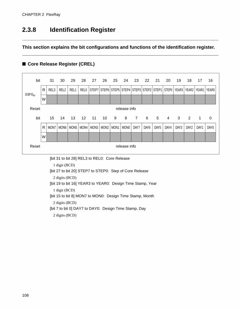
CHAPTER 2 FlexRay
2.3.8 Identification Register
This section explains the bit configurations and functions of the identification register.
■ Core Release Register (CREL)
[bit 31 to bit 28] REL3 to REL0: Core Release
1 digit (BCD)
[bit 27 to bit 20] STEP7 to STEP0: Step of Core Release
2 digits (BCD)
[bit 19 to bit 16] YEAR3 to YEAR0: Design Time Stamp, Year
1 digit (BCD)
[bit 15 to bit 8] MON7 to MON0: Design Time Stamp, Month
2 digits (BCD)
[bit 7 to bit 0] DAY7 to DAY0: Design Time Stamp, Day
2 digits (BCD)
bit 31 30 29 28 27 26 25 24 23 22 21 20 19 18 17 16
03F0H
R REL3 REL2 REL1 REL0 STEP7 STEP6 STEP5 STEP4 STEP3 STEP2 STEP1 STEP0 YEAR3 YEAR2 YEAR1 YEAR0
W
Reset release info
bit 15 14 13 12 11 10 9 8 7 6 5 4 3 2 1 0
R MON7 MON6 MON5 MON4 MON3 MON2 MON1 MON0 DAY7 DAY6 DAY5 DAY4 DAY3 DAY2 DAY1 DAY0
W
Reset release info
108

CHAPTER 2 FlexRay
■ Endian Register (ENDN)
[bit 31 to bit 0] ETV31 to ETV0: Endianness Test Value
Test value 87654321H
bit 31 30 29 28 27 26 25 24 23 22 21 20 19 18 17 16
03F4H
R ETV31 ETV30 ETV29 ETV28 ETV27 ETV26 ETV25 ETV24 ETV23 ETV22 ETV21 ETV20 ETV19 ETV18 ETV17 ETV16
W
Reset 1 0 0 0 0 1 1 1 0 1 1 0 0 1 0 1
bit 15 14 13 12 11 10 9 8 7 6 5 4 3 2 1 0
R ETV15 ETV14 ETV13 ETV12 ETV11 ETV10 ETV9 ETV8 ETV7 ETV6 ETV5 ETV4 ETV3 ETV2 ETV1 ETV0
W
Reset 0 1 0 0 0 0 1 1 0 0 1 0 0 0 0 1
109

CHAPTER 2 FlexRay
2.3.9 Input Buffer
This section explains the bit configurations and functions of the input buffer.
■ Input BufferThe input buffer consists of a double buffer; the input buffer host and input buffer shadow. Data is
transferred from the input buffer shadow to the message RAM while the host is able to write into the input
buffer host. The header section and data section are stored into the input buffer before they are transferred
to the selected message buffer. The input buffer is also used to update the configuration of the message
buffer of the message RAM, and the data section of the transmit buffer.
The message buffer status is automatically reset to "0" when updating the header section in the message
RAM from the input buffer as described in "■ Message Buffer Status Register (MBS)".
Modify the header section of a message buffer which belongs to the receive FIFO only in the
DEFAULT_CONFIG state or CONFIG state.
See "■ Data Transmission from the Message RAM to the Output Buffer" for details of data transfers
between the input buffer (IBF) and the message RAM.
■ Write Data Section Register (WRDS1 to WRDS64)The write data section register is set with data before it is transferred to the data section of the message
buffer. The data (DWn) is written into the message RAM according to the order of transmission from DW1
(byte 0, byte 1) to DWPL (PL = the number of data items in 2-byte units defined by the payload length).
[bit 31 to bit 0] MD31 to MD0: Message Data
MD7 to MD0 = DWn, byten-1
bit 31 30 29 28 27 26 25 24 23 22 21 20 19 18 17 16
0400Hto
04FCH
R
MD31 MD30 MD29 MD28 MD27 MD26 MD25 MD24 MD23 MD22 MD21 MD20 MD19 MD18 MD17 MD16W
Reset 0 0 0 0 0 0 0 0 0 0 0 0 0 0 0 0
bit 15 14 13 12 11 10 9 8 7 6 5 4 3 2 1 0
RMD15 MD14 Md13 MD12 MD11 MD10 MD9 MD8 MD7 MD6 MD5 MD4 MD3 MD2 MD1 MD0
W
Reset 0 0 0 0 0 0 0 0 0 0 0 0 0 0 0 0
110

CHAPTER 2 FlexRay
MD15 to MD8 = DWn, byten
MD23 to MD16 = DWn+1, byten+1
MD31 to MD24 = DWn+1, byten+2
Note:
DW127 is assigned to WRDS64: MD15 to MD0. In this case, WRDS64: MD31 to MD16 is unused (undefined data). The input buffer RAM is initialized to "0" by either the completion of a hardware reset, or the CHI command CLEAR_RAMS (CMD3 to CMD0 = 1100B).
■ Write Header Section Register 1 (WRHS1)
[bit 29] MBI: Message Buffer Interrupt
This bit enables transmission and reception interrupts to the message buffers. SIR:RXI or SIR:MBSI are set to "1" after a message is received into the receive buffer. Also, the SIR:TXI flag is set to "1" after a message is transmitted successfully from the transmit buffer.
"1" = Enable transmission and reception interrupts on the corresponding message buffer
"0" = Disable transmission and reception interrupts on the corresponding message buffer
[bit 28] TXM: Transmission Mode
This bit selects the transmission mode (see "■ Transmit Buffer").
"1" = Single shot mode
"0" = Continuous mode
[bit 27] PPIT: Payload Preamble Indicator Transmit
This bit is used to control the payload preamble indicator status for a transmit frame. When this bit is set to the static message buffer, each message buffer retains network management information. However, when this bit is set to the dynamic message buffer, the first 2 bytes of the payload segment are used for message ID filtering. The message ID filtering of receive frames is not supported by the FlexRay controller.
"1" = Set the payload preamble indicator
"0" = Not to set the payload preamble indicator
bit 31 30 29 28 27 26 25 24 23 22 21 20 19 18 17 16
0500H
R 0 0MBI TXM PPIT CFG CHB CHA
0CYC6 CYC5 CYC4 CYC3 CYC2 CYC1 CYC0
W
Reset 0 0 0 0 0 0 0 0 0 0 0 0 0 0 0 0
bit 15 14 13 12 11 10 9 8 7 6 5 4 3 2 1 0
R 0 0 0 0 0FID10 FID9 FID8 FID7 FID6 FID5 FID4 FID3 FID2 FID1 FID0
W
Reset 0 0 0 0 0 0 0 0 0 0 0 0 0 0 0 0
111

CHAPTER 2 FlexRay
[bit 26] CFG: Message Buffer Configuration Bit
This bit is used to configure a buffer as a transmit buffer or a receive buffer. The message buffers which belong to the receive FIFO become invalid.
"1" = The corresponding buffer is configured as a transmit buffer.
"0" = The corresponding buffer is configured as a receive buffer.
[bit 25, bit 24] CHB, CHA Channel Filter Control
This 2-bit associated with each buffer functions as the filter for the receive buffer and also as the control field for the transmit buffer.
Note:
When the message buffer is set for a dynamic segment and both channel filtering fields (CHA, CHB) are set to "1", the frame is not transmitted and the receive frame has no effect on the operation (the same function as for CHA = CHB = 0).
[bit 22 to bit 16] CYC6 to CYC0: Cycle Code
This 7-bit code determines the cycle set which is used for cycle counter filtering. See "■ Cycle Counter Filtering" for details on cycle code settings.
[bit 10 to bit 0] FID10 to FID0: Frame ID
These bits indicate the frame ID of the selected message buffer. The frame ID defines the slot number for each message transmission and reception. A message buffer with frame ID = 0 is invalid.
CHA CHBTransmit Buffer
transmit frame onReceive Buffer
store frame received from
1 1both channels(static segment only)
ch.A or ch.B (store first semantically valid frame, static segment only)
1 0 ch.A ch.A
0 1 ch.B ch.B
1 0 no transmission ignore frame
112
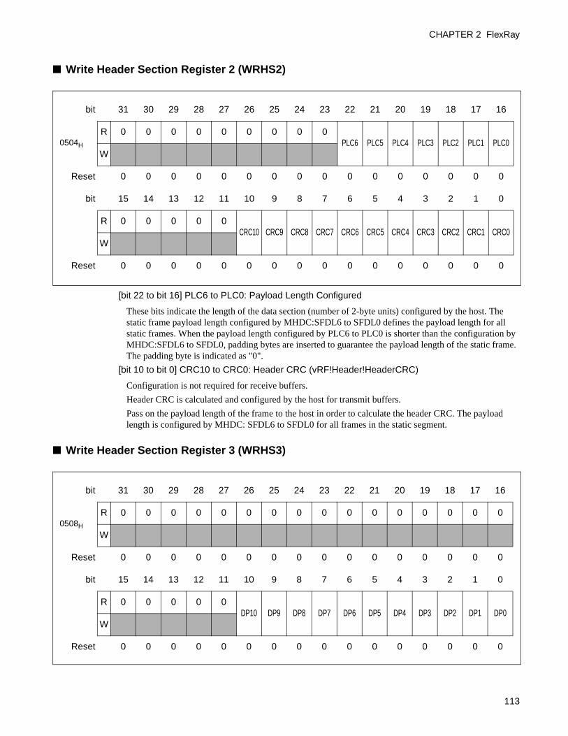
CHAPTER 2 FlexRay
■ Write Header Section Register 2 (WRHS2)
[bit 22 to bit 16] PLC6 to PLC0: Payload Length Configured
These bits indicate the length of the data section (number of 2-byte units) configured by the host. The static frame payload length configured by MHDC:SFDL6 to SFDL0 defines the payload length for all static frames. When the payload length configured by PLC6 to PLC0 is shorter than the configuration by MHDC:SFDL6 to SFDL0, padding bytes are inserted to guarantee the payload length of the static frame. The padding byte is indicated as "0".
[bit 10 to bit 0] CRC10 to CRC0: Header CRC (vRF!Header!HeaderCRC)
Configuration is not required for receive buffers.
Header CRC is calculated and configured by the host for transmit buffers.
Pass on the payload length of the frame to the host in order to calculate the header CRC. The payload length is configured by MHDC: SFDL6 to SFDL0 for all frames in the static segment.
■ Write Header Section Register 3 (WRHS3)
bit 31 30 29 28 27 26 25 24 23 22 21 20 19 18 17 16
0504H
R 0 0 0 0 0 0 0 0 0PLC6 PLC5 PLC4 PLC3 PLC2 PLC1 PLC0
W
Reset 0 0 0 0 0 0 0 0 0 0 0 0 0 0 0 0
bit 15 14 13 12 11 10 9 8 7 6 5 4 3 2 1 0
R 0 0 0 0 0CRC10 CRC9 CRC8 CRC7 CRC6 CRC5 CRC4 CRC3 CRC2 CRC1 CRC0
W
Reset 0 0 0 0 0 0 0 0 0 0 0 0 0 0 0 0
bit 31 30 29 28 27 26 25 24 23 22 21 20 19 18 17 16
0508H
R 0 0 0 0 0 0 0 0 0 0 0 0 0 0 0 0
W
Reset 0 0 0 0 0 0 0 0 0 0 0 0 0 0 0 0
bit 15 14 13 12 11 10 9 8 7 6 5 4 3 2 1 0
R 0 0 0 0 0DP10 DP9 DP8 DP7 DP6 DP5 DP4 DP3 DP2 DP1 DP0
W
Reset 0 0 0 0 0 0 0 0 0 0 0 0 0 0 0 0
113

CHAPTER 2 FlexRay
[bit 10 to bit 0] DP10 to DP0: Data Pointer
These bits indicate the pointer to the first 32-bit of the data section of the message buffer.
■ Input Buffer Command Mask Register (IBCM)This register configures the update method of the message buffer selected by the IBCR register. When the
IBF host and IBF shadow is swapped, mask bit LHSH, LDSH, STXRH and mask bit LHSS, LDSS,
STXRS are also swapped.
[bit 17] STXRS: Set Transmission Request Shadow
"1" = Flags TXR127 to TXR0 have been set and the message in the transmit buffer is being
released. Or, these operations have completed.
"0" = Flags TXR127 to TXR0 are being reset.
[bit 16] LDSS: Load Data Section Shadow
"1" = Transfer of the data section from the input buffer to the message RAM is in progress. Or, the
transfer has completed.
"0" = Transfer of the data section from the input buffer to the message RAM is not in progress
[bit 2] STXRH: Set Transmission Request Host
When this bit is set to "1", flags TXR127 to TXR0 of the selected message buffer are set to "1" within the TXRQ1/TXRQ2/TXRQ3/TXRQ4 registers and the message in that transmit buffer is released. These flags are cleared after completing the transmission in single shot mode.
"1" = Set flags TXR127 to TXR0 and release the message in the transmit buffer
"0" = Reset flags TXR127 to TXR0
[bit 1] LDSH: Load Data Section Host
"1" = Transfer the data section from the input buffer to the message RAM
"0" = Not to transfer the data section
[bit 0] LHSH: Load Header Section Host
"1" = Transfer the header section from the input buffer to the message RAM
"0" = Not to transfer the header section
bit 31 30 29 28 27 26 25 24 23 22 21 20 19 18 17 16
0510H
R 0 0 0 0 0 0 0 0 0 0 0 0 0 0 STXRS LDSS
W
Reset 0 0 0 0 0 0 0 0 0 0 0 0 0 0 0 0
bit 15 14 13 12 11 10 9 8 7 6 5 4 3 2 1 0
R 0 0 0 0 0 0 0 0 0 0 0 0 0STXRH LDSH LHSH
W
Reset 0 0 0 0 0 0 0 0 0 0 0 0 0 0 0 0
114
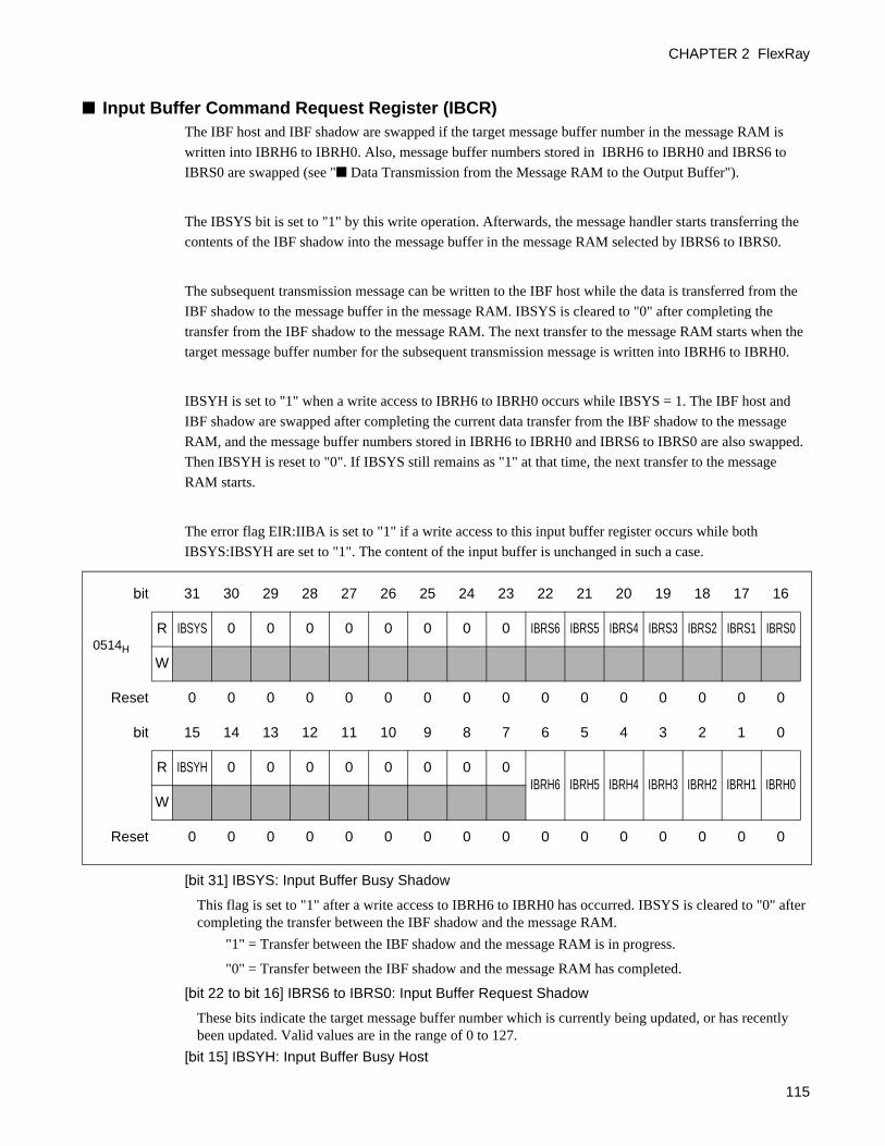
CHAPTER 2 FlexRay
■ Input Buffer Command Request Register (IBCR)The IBF host and IBF shadow are swapped if the target message buffer number in the message RAM is
written into IBRH6 to IBRH0. Also, message buffer numbers stored in IBRH6 to IBRH0 and IBRS6 to
IBRS0 are swapped (see "■ Data Transmission from the Message RAM to the Output Buffer").
The IBSYS bit is set to "1" by this write operation. Afterwards, the message handler starts transferring the
contents of the IBF shadow into the message buffer in the message RAM selected by IBRS6 to IBRS0.
The subsequent transmission message can be written to the IBF host while the data is transferred from the
IBF shadow to the message buffer in the message RAM. IBSYS is cleared to "0" after completing the
transfer from the IBF shadow to the message RAM. The next transfer to the message RAM starts when the
target message buffer number for the subsequent transmission message is written into IBRH6 to IBRH0.
IBSYH is set to "1" when a write access to IBRH6 to IBRH0 occurs while IBSYS = 1. The IBF host and
IBF shadow are swapped after completing the current data transfer from the IBF shadow to the message
RAM, and the message buffer numbers stored in IBRH6 to IBRH0 and IBRS6 to IBRS0 are also swapped.
Then IBSYH is reset to "0". If IBSYS still remains as "1" at that time, the next transfer to the message
RAM starts.
The error flag EIR:IIBA is set to "1" if a write access to this input buffer register occurs while both
IBSYS:IBSYH are set to "1". The content of the input buffer is unchanged in such a case.
[bit 31] IBSYS: Input Buffer Busy Shadow
This flag is set to "1" after a write access to IBRH6 to IBRH0 has occurred. IBSYS is cleared to "0" after completing the transfer between the IBF shadow and the message RAM.
"1" = Transfer between the IBF shadow and the message RAM is in progress.
"0" = Transfer between the IBF shadow and the message RAM has completed.
[bit 22 to bit 16] IBRS6 to IBRS0: Input Buffer Request Shadow
These bits indicate the target message buffer number which is currently being updated, or has recently been updated. Valid values are in the range of 0 to 127.
[bit 15] IBSYH: Input Buffer Busy Host
bit 31 30 29 28 27 26 25 24 23 22 21 20 19 18 17 16
0514H
R IBSYS 0 0 0 0 0 0 0 0 IBRS6 IBRS5 IBRS4 IBRS3 IBRS2 IBRS1 IBRS0
W
Reset 0 0 0 0 0 0 0 0 0 0 0 0 0 0 0 0
bit 15 14 13 12 11 10 9 8 7 6 5 4 3 2 1 0
R IBSYH 0 0 0 0 0 0 0 0IBRH6 IBRH5 IBRH4 IBRH3 IBRH2 IBRH1 IBRH0
W
Reset 0 0 0 0 0 0 0 0 0 0 0 0 0 0 0 0
115

CHAPTER 2 FlexRay
This flag is set to "1" if a write access to IBRH6 to IBRH0 occurs while IBSYS is "1". This flag is cleared to "0" after completing the current data transfer from the IBF shadow to the message RAM.
"1" = Message transfer is being suspended.
"0" = Message transfer is not being suspended.
[bit 6 to bit 0] IBRH6 to IBRH0: Input Buffer Request Host
These bits select the target message buffer number in the message RAM in order to transfer data from the input buffer. Valid values are in the range of 0 to 127.
116

CHAPTER 2 FlexRay
2.3.10 Output Buffer
This section explains the bit configurations and functions of the output buffer.
■ Output BufferThe output buffer consists of a double buffer; the output buffer host and output buffer shadow, and is used
to read the message buffer from the message RAM. The selected message buffer is transferred from the
message RAM to the output buffer shadow while the host is able to read from the output buffer host. See
"■ Data Transmission from the Message RAM to the Output Buffer" for details of data transfers between
the message RAM and the output buffer (OBF).
■ Read Data Section Register (RDDS1 to RDDS64)The read data section register is set with data read from the data section of the message buffer. The data
(DWn) is read from the message RAM according to the order of reception from DW1 (byte 0, byte 1) to
DWPL (PL = the number of data items in 2-byte units defined by the payload length).
[bit 31 to bit 0] MD31 to MD0: Message Data
MD7 to MD0 = DWn, byten-1
MD15 to MD8 = DWn, byten
MD23 to MD16 = DWn+1, byten+1
MD31 to MD24 = DWn+1, byten+2
Note:
DW127 is assigned to RDDS64: MD15 to MD0. In this case, RDDS64: MD31 to MD16 is unused (undefined data).
The output buffer RAM is initialized to "0" by either the completion of a hardware reset, or the CHI command CLEAR_RAMS (CMD3 to CMD0 = 1100B).
bit 31 30 29 28 27 26 25 24 23 22 21 20 19 18 17 16
0600Hto
06FCH
R MD31 MD30 MD29 MD28 MD27 MD26 MD25 MD24 MD23 MD22 MD21 MD20 MD19 MD18 MD17 MD16
W
Reset 0 0 0 0 0 0 0 0 0 0 0 0 0 0 0 0
bit 15 14 13 12 11 10 9 8 7 6 5 4 3 2 1 0
R MD15 MD14 MD13 MD12 MD11 MD10 MD9 MD8 MD7 MD6 MD5 MD4 MD3 MD2 MD1 MD0
W
Reset 0 0 0 0 0 0 0 0 0 0 0 0 0 0 0 0
117

CHAPTER 2 FlexRay
■ Read Header Section Register 1 (RDHS1)
The following values are set through WRHS1.
FID10 to FID0 Frame ID
CYC6 to CYC0 Cycle Code
CHA, CHB Channel Filter Control
CFG Message Buffer Configuration Bit
PPIT Payload Preamble Indicator Transmit
TXM Transmission Mode
MBI Message Buffer Interrupt
FID10 to FID0 retains the receive frame ID while CYC6 to CYC0, CHA, CHB , CFG, PPIT, TXM, MBI
are reset to "0" when the message buffer read from the message RAM belongs to the receive FIFO.
■ Read Header Section Register 2 (RDHS2)
bit 31 30 29 28 27 26 25 24 23 22 21 20 19 18 17 16
0700H
R 0 0 MBI TXM PPIT CFG CHB CHA 0 CYC6 CYC5 CYC4 CYC3 CYC2 CYC1 CYC0
W
Reset 0 0 0 0 0 0 0 0 0 0 0 0 0 0 0 0
bit 15 14 13 12 11 10 9 8 7 6 5 4 3 2 1 0
R 0 0 0 0 0 FID10 FID9 FID8 FID7 FID6 FID5 FID4 FID3 FID2 FID1 FID0
W
Reset 0 0 0 0 0 0 0 0 0 0 0 0 0 0 0 0
bit 31 30 29 28 27 26 25 24 23 22 21 20 19 18 17 16
0704H
R 0 PLR6 PLR5 PLR4 PLR3 PLR2 PLR1 PLR0 0 PLC6 PLC5 PLC4 PLC3 PLC2 PLC1 PLC0
W
Reset 0 0 0 0 0 0 0 0 0 0 0 0 0 0 0 0
bit 15 14 13 12 11 10 9 8 7 6 5 4 3 2 1 0
R 0 0 0 0 0 CRC10 CRC9 CRC8 CRC7 CRC6 CRC5 CRC4 CRC3 CRC2 CRC1 CRC0
W
Reset 0 0 0 0 0 0 0 0 0 0 0 0 0 0 0 0
118

CHAPTER 2 FlexRay
[bit 30 to bit 24] PLR6 to PLR0: Payload Length Received (vRF!Header!Length)
These bits indicate the value of the payload length updated by the receive frame.
[bit 22 to bit 16] PLC6 to PLC0: Payload Length Configured
These bits indicate the length of the data section (number of 2-byte units) configured by the host.
The following operations take place when a message is stored in the message buffer in relation to the receive payload length or configuration payload length.
PLR6 to PLR0 > PLC6 to PLC0:Payload data stored in the message buffer is shortened to a payload length configured in PLC6 to PLC0 or PLC6 to PLC0 + 1.
PLR6 to PLR60 > PLC6 to PLC0:Receive payload data is stored in the data section of the message buffer. Remaining data bytes in the data section configured by PLC6 to PLC0 are filled with undefined data.
PLR6 to PLR0 = 0: The data section of the message buffer is filled with undefined data.
PLC6 to PLC0 = 0: There is no data section in the message buffer. Data is not stored in the data section of the message buffer.
[bit 10 to bit 0] CRC10 to CRC0: Header CRC (vRF!Header!HeaderCRC)
Header CRC is updated by the receive frame for the receive buffers.
Header CRC configured by the message transfer from the input buffer is displayed for the transmit buffers.
Note:
The message RAM consists of 4 bytes. When receive data is stored in the data section of the message buffer, the number of data words in 2-byte units written into the message buffer is the value in PLC6 to PLC0 rounded up to the nearest even number. PLC6 to PLC0 is configured identically for all message buffers to the receive FIFO. Header 2 is updated by the data frame.
■ Read Header Section Register 3 (RDHS3)
bit 31 30 29 28 27 26 25 24 23 22 21 20 19 18 17 16
0708H
R 0 0 RES PPI NFI SYN SFI RCI 0 0 RCC5 RCC4 RCC3 RCC2 RCC1 RCC0
W
Reset 0 0 0 0 0 0 0 0 0 0 0 0 0 0 0 0
bit 15 14 13 12 11 10 9 8 7 6 5 4 3 2 1 0
R 0 0 0 0 0 DP 10 DP9 DP8 DP7 DP6 DP5 DP4 DP3 DP2 DP1 DP0
W
Reset 0 0 0 0 0 0 0 0 0 0 0 0 0 0 0 0
119

CHAPTER 2 FlexRay
[bit 29] RES: Reserved Bit (vRF!Header!Reserved)
This bit reflects the status of the received reserved bit.
[bit 28] PPI: Payload Preamble Indicator (vRF!Header!PPIndicator)
This bit indicates whether the network management vector or the message ID is included in the payload segment of the receive frame.
"1" = The network management vector is included at the beginning of the payload if it is a static
segment.
The message ID is included at the beginning of the payload if it is a dynamic segment.
"0" = Neither the network management vector nor the message ID is included in the payload
segment of the receive frame.
[bit 27] NFI: Null Frame Indicator (vRF!Header!NFIndicator)
There is no valid data in the payload segment of the receive frame when this bit is "0".
"1" = The receive frame is not a null frame.
"0" = The receive frame is a null frame.
[bit 26] SYN: Sync Frame Indicator (vRF!Header!SyFIndicator)
This bit indicates that the receive frame is a sync frame.
"1" = The receive frame is a sync frame.
"0" = The receive frame is not a sync frame.
[bit 25] SFI: Startup Frame Indicator (vRF!Header!SuFIndicator)
This bit indicates that the receive frame is a startup frame.
"1" = The receive frame is a startup frame.
"0" = The receive frame is not a startup frame.
[bit 24] RCI: Received on Channel Indicator (vSS!Channel)
This bit indicates the channel where the receive frame that updates each receive buffer has been received.
"1" = The frame has been received through ch.A.
"0" = The frame has been received through ch.B.
[bit 21 to bit 16] RCC5 to RCC0: Receive Cycle Count (vRF!Header!CycleCounter)
These bits indicate the cycle counter value updated by the receive frame.
[bit 10 to bit 0] DP10 to DP0: Data Pointer
These bits indicate the pointer to the first 32-bit of the data section of the message buffer.
Note:
Header 3 is updated by the data frame.
■ Message Buffer Status Register (MBS)The assigned channel is updated at the message buffer status channel at the end of the slot which is next to
the one assigned to the message buffer. When only one channel (A or B) is assigned to a message buffer,
the status flag for the other channel is cleared to "0". Whereas if both channels are assigned to a message
buffer, status flags for both channels are updated.
The message buffer status always indicates the latest status of the slot assigned to the message buffer.
120

CHAPTER 2 FlexRay
When the host updates the message buffer through the input buffer, all MBS flags are reset even when the
IBCM bit is set. See "2.7.7 Filtering and Masking", "2.7.8 Transmission Procedure" and "2.7.9 Reception
Procedure" for details on transmission and reception filtering. MBC flags of message buffers for MBSC1,
MBSC2, MBSC3 and MBSC4 registers are always set when the message handler changes any one of the
VFRA, VFRA, SEOA, SEOB, CEOA, SVOA, SVOB, TCIA, TCIB, ESA, ESB, MLST, FTA or FTB flags.
● Status flags associated with receive buffers
[bit 29] RESS: Reserved Bit Status (vRF!Header!Reserved)
This bit indicates the status of the reserve bit for receptions. The reserved bit is set to "0" when it is transmitted.
[bit 28] PPIS: Payload Preamble Indicator Status (vRF!Header!PPIndicator)
The payload preamble indicator status defines whether the network management vector or message ID is included in the payload segment of the receive frame.
"1" = The network management vector is included if it is a static segment.
The message ID is included if it is a dynamic segment.
"0" = Not included.
[bit 27] NFIS: Null Frame Indicator Status (vRF!Header!NFIndicator)
"1" = The receive frame is not a null frame.
"0" = The receive frame is a null frame.
[bit 26] SYNS: Sync Frame Indicator Status (vRF!Header!SyFIndicator)
"1" = A sync frame has been received.
"0" = A sync frame has not been received.
[bit 25] SFIS: Startup Frame Indicator Status (vRF!Header!SuFIndicator)
"1" = A startup frame has been received.
"0" = A startup frame has not been received.
[bit 24] RCIS: Received on Channel Indicator Status (vSS!Channel)
"1" = A frame has been received through ch.A.
"0" = A frame has been received through ch.B.
bit 31 30 29 28 27 26 25 24 23 22 21 20 19 18 17 16
070CH
R 0 0 RESS PPIS NFIS SYNS SFIS RCIS 0 0 CCS5 CCS4 CCS3 CCS2 CCS1 CCS0
W
Reset 0 0 0 0 0 0 0 0 0 0 0 0 0 0 0 0
bit 15 14 13 12 11 10 9 8 7 6 5 4 3 2 1 0
R FTB FTA 0 MLST ESB ESA TCIB TCIA SVOB SVOA CEOB CEOA SEOB SEOA VFRB VFRA
W
Reset 0 0 0 0 0 0 0 0 0 0 0 0 0 0 0 0
121

CHAPTER 2 FlexRay
[bit 21 to bit 16] CCS5 to CCS0 Cycle Count Status
A cycle count occurs when the status is updated.
The following status bits are updated by both the valid and invalid frame data. The previous value is
retained if a valid frame is not received.
[bit 15] FTB: Frame Transmitted to ch.B
This bit indicates that a data frame has been transmitted to ch.B.
"1" = A data frame has been transmitted to ch.B.
"0" = A data frame has not been transmitted to ch.B.
[bit 14] FTA: Frame Transmitted to ch.A
This bit indicates that a data frame has been transmitted to ch.A.
"1" = A data frame has been transmitted to ch.A.
"0" = A data frame has not been transmitted to ch.A.
[bit 12] MLST: Message Lost
This bit indicates that the message was not read before the message buffer was overwritten by the new message. The reception of a null frame has no effect except on the message buffer for the receive FIFO.
"1" = Unread message has been overwritten.
"0" = No message has been lost.
Note:
Only the host can reset MLST, FTA and FTB. Therefore, the cycle count status (CCS5 to CCS0) is valid in the cycle that sets the bits to "1".
[bit 11] ESB: Empty Slot ch.B
An empty slot indicates an idle status of the bus, in other words, no frame transmission is detected . This status is checked on static slots and dynamic slots.
"1" = The bus is idle in the slot assigned for ch.B.
"0" = The bus is not idle in the slot assigned for ch.B.
[bit 10] ESA: Empty Slot ch.A
An empty slot indicates an idle status of the bus, in other words, no frame transmission is detected . This status is checked on static slots and dynamic slots.
"1" = The bus is idle in the slot assigned for ch.A.
"0" = The bus is not idle in the slot assigned for ch.A.
● Status flags associated with transmit buffers
[bit 9] TCIB: Transmission Collision Indication ch.B (vSS!TxConflictB)
This bit is set to "1" when a transmission collision is detected on ch.B.
"1" = A transmission collision has been detected on ch.B.
"0" = A transmission collision has not been detected on ch.B.
[bit 8] TCIA: Transmission Collision Indication ch.A (vSS!TxConflictA)
This bit is set to "1" when a transmission collision is detected on ch.A.
122

CHAPTER 2 FlexRay
"1" = A transmission collision has been detected on ch.A.
"0" = A transmission collision has not been detected on ch.A.
● Status flags associated with receive and transmit buffers
[bit 7] SVOB: Slot Boundary Violation Observed on ch.B (vSS!BViolationB)
This bit indicates that a slot boundary violation has been detected on the slot assigned to ch.B. This means that the channel was active at the opening or closing of the configured slot.
"1" = A slot boundary violation has been detected on ch.B.
"0" = A slot boundary violation has not been detected on ch.B.
[bit 6] SVOA: Slot Boundary Violation Observed on ch.A (vSS!BViolationA)
This bit indicates that a slot boundary violation has been detected on the slot assigned to ch.A. This means that the channel was active at the opening or closing of the configured slot.
"1" = A slot boundary violation has been detected on ch.A.
"0" = A slot boundary violation has not been detected on ch.A.
[bit 5] CEOB: Content Error Observed on ch.B (vSS!ContentErrorB)
This bit indicates that a content error has been detected on the slot assigned to ch.B.
"1" = A content error has been detected on ch.B.
"0" = A content error has not been detected on ch.B.
[bit 4] CEOA: Content Error Observed on ch.A (vSS!ContentErrorA)
This bit indicates that a content error has been detected on the slot assigned to ch.A.
"1" = A content error has been detected on ch.A.
"0" = A content error has not been detected on ch.A.
[bit 3] SEOB: Syntax Error Observed on ch.B (vSS!SyntaxErrorB)
This bit indicates that a syntax error has been detected on the slot assigned to ch.B.
"1" = A syntax error has been detected on ch.B.
"0" = A syntax error has not been detected on ch.B.
[bit 2] SEOA: Syntax Error Observed on ch.A (vSS!SyntaxErrorA)
This bit indicates that a syntax error has been detected on the slot assigned to ch.A.
"1" = A syntax error has been detected on ch.A.
"0" = A syntax error has not been detected on ch.A.
[bit 1] VFRB: Valid Frame Received on ch.B (vSS!ValidFrameB)
This bit is set to "1" when a valid frame is received through ch.B.
"1" = A valid frame has been received through ch.B.
"0" = A valid frame has not been received through ch.B.
[bit 0] VFRA: Valid Frame Received on ch.A (vSS!ValidFrameA)
This bit is set to "1" when a valid frame is received through ch.A.
"1" = A valid frame has been received through ch.A.
"0" = A valid frame has not been received through ch.A.
123
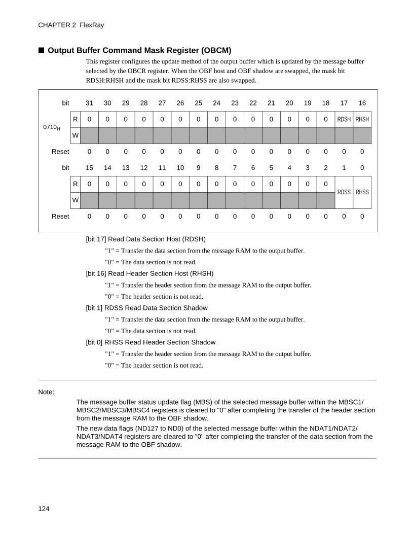
CHAPTER 2 FlexRay
■ Output Buffer Command Mask Register (OBCM)This register configures the update method of the output buffer which is updated by the message buffer
selected by the OBCR register. When the OBF host and OBF shadow are swapped, the mask bit
RDSH:RHSH and the mask bit RDSS:RHSS are also swapped.
[bit 17] Read Data Section Host (RDSH)
"1" = Transfer the data section from the message RAM to the output buffer.
"0" = The data section is not read.
[bit 16] Read Header Section Host (RHSH)
"1" = Transfer the header section from the message RAM to the output buffer.
"0" = The header section is not read.
[bit 1] RDSS Read Data Section Shadow
"1" = Transfer the data section from the message RAM to the output buffer.
"0" = The data section is not read.
[bit 0] RHSS Read Header Section Shadow
"1" = Transfer the header section from the message RAM to the output buffer.
"0" = The header section is not read.
Note:
The message buffer status update flag (MBS) of the selected message buffer within the MBSC1/MBSC2/MBSC3/MBSC4 registers is cleared to "0" after completing the transfer of the header section from the message RAM to the OBF shadow.
The new data flags (ND127 to ND0) of the selected message buffer within the NDAT1/NDAT2/NDAT3/NDAT4 registers are cleared to "0" after completing the transfer of the data section from the message RAM to the OBF shadow.
bit 31 30 29 28 27 26 25 24 23 22 21 20 19 18 17 16
0710H
R 0 0 0 0 0 0 0 0 0 0 0 0 0 0 RDSH RHSH
W
Reset 0 0 0 0 0 0 0 0 0 0 0 0 0 0 0 0
bit 15 14 13 12 11 10 9 8 7 6 5 4 3 2 1 0
R 0 0 0 0 0 0 0 0 0 0 0 0 0 0RDSS RHSS
W
Reset 0 0 0 0 0 0 0 0 0 0 0 0 0 0 0 0
124
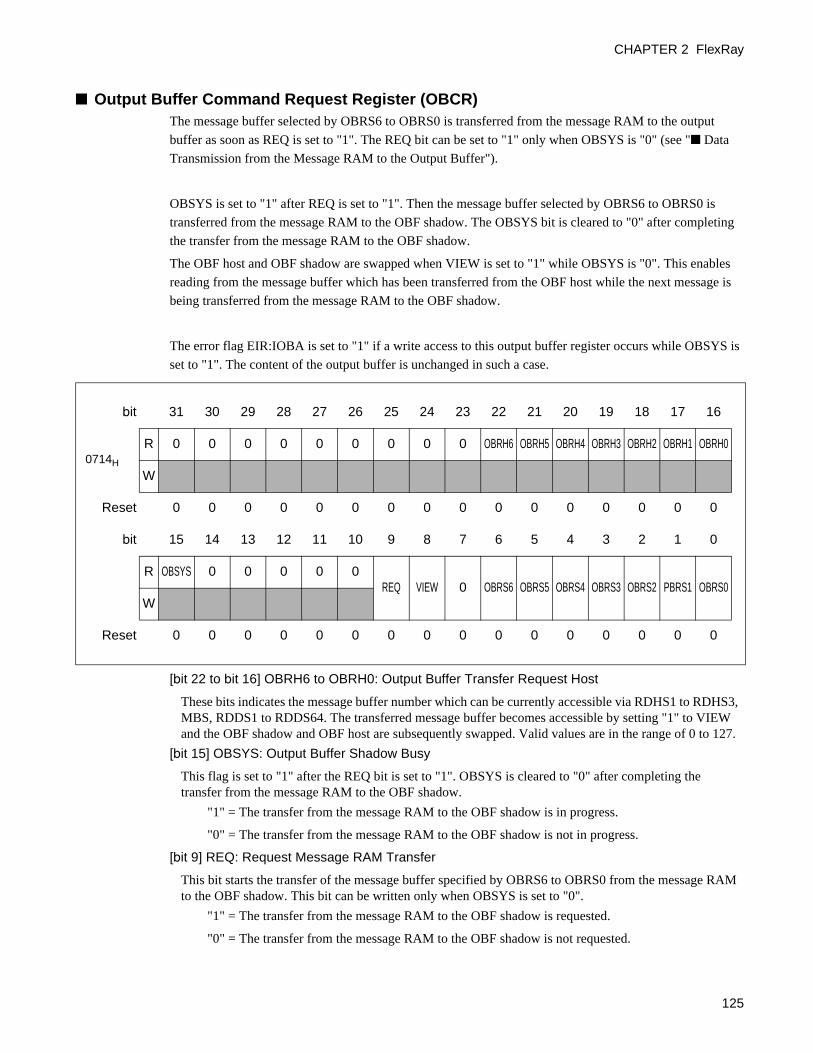
CHAPTER 2 FlexRay
■ Output Buffer Command Request Register (OBCR)The message buffer selected by OBRS6 to OBRS0 is transferred from the message RAM to the output
buffer as soon as REQ is set to "1". The REQ bit can be set to "1" only when OBSYS is "0" (see "■ Data
Transmission from the Message RAM to the Output Buffer").
OBSYS is set to "1" after REQ is set to "1". Then the message buffer selected by OBRS6 to OBRS0 is
transferred from the message RAM to the OBF shadow. The OBSYS bit is cleared to "0" after completing
the transfer from the message RAM to the OBF shadow.
The OBF host and OBF shadow are swapped when VIEW is set to "1" while OBSYS is "0". This enables
reading from the message buffer which has been transferred from the OBF host while the next message is
being transferred from the message RAM to the OBF shadow.
The error flag EIR:IOBA is set to "1" if a write access to this output buffer register occurs while OBSYS is
set to "1". The content of the output buffer is unchanged in such a case.
[bit 22 to bit 16] OBRH6 to OBRH0: Output Buffer Transfer Request Host
These bits indicates the message buffer number which can be currently accessible via RDHS1 to RDHS3, MBS, RDDS1 to RDDS64. The transferred message buffer becomes accessible by setting "1" to VIEW and the OBF shadow and OBF host are subsequently swapped. Valid values are in the range of 0 to 127.
[bit 15] OBSYS: Output Buffer Shadow Busy
This flag is set to "1" after the REQ bit is set to "1". OBSYS is cleared to "0" after completing the transfer from the message RAM to the OBF shadow.
"1" = The transfer from the message RAM to the OBF shadow is in progress.
"0" = The transfer from the message RAM to the OBF shadow is not in progress.
[bit 9] REQ: Request Message RAM Transfer
This bit starts the transfer of the message buffer specified by OBRS6 to OBRS0 from the message RAM to the OBF shadow. This bit can be written only when OBSYS is set to "0".
"1" = The transfer from the message RAM to the OBF shadow is requested.
"0" = The transfer from the message RAM to the OBF shadow is not requested.
bit 31 30 29 28 27 26 25 24 23 22 21 20 19 18 17 16
0714H
R 0 0 0 0 0 0 0 0 0 OBRH6 OBRH5 OBRH4 OBRH3 OBRH2 OBRH1 OBRH0
W
Reset 0 0 0 0 0 0 0 0 0 0 0 0 0 0 0 0
bit 15 14 13 12 11 10 9 8 7 6 5 4 3 2 1 0
R OBSYS 0 0 0 0 0REQ VIEW 0 OBRS6 OBRS5 OBRS4 OBRS3 OBRS2 PBRS1 OBRS0
W
Reset 0 0 0 0 0 0 0 0 0 0 0 0 0 0 0 0
125

CHAPTER 2 FlexRay
[bit 8] VIEW: Swap Shadow Buffer and Host Buffer
This bit swaps the OBF shadow and OBF host. This bit can be written only when OBSYS is set to "0".
"1" = Swap the OBF shadow and OBF host.
"0" = Not to swap the OBF shadow and OBF host.
[bit 6 to bit 0] OBRS6 to OBRS0: Output Buffer Transfer Request Shadow
These bits indicate the message buffer number for the transfer from the message RAM to the OBF shadow. Valid values are in the range of 0 to 127. When the first message number within the receive FIFO is written to this register, the message buffer specified by GET Index(GIDX), (See "2.7.10 FIFO Function") is transferred to the OBF shadow.
126

CHAPTER 2 FlexRay
2.4 FlexRay Operations
This section explains the operation of the FlexRay.
■ FlexRay OperationsMB88121B supports the 16-bit non-multiplex bus, 16-bit multiplex bus and SPI bus. The mode is
determined as follows depending on the settings of the MD2 to MD0 pins and the MDE2 to MDE0 pins.
Note: Any other pin settings are prohibited. "x" is undefined value.
■ 16-bit Non-multiplex Parallel Bus Timing The following illustrates the 16-bit non-multiplex parallel timing.
● Read operations
Figure 2.4-1 FR460 Mode Read Timing (16-bit Non-multiplex Bus Mode)
When the CS pin and RD pin become "L", data is output to the D15 to D0 pins, the RDY pin is set to "L" at
the rising of the next BCLK pin and waits for the CPU. When data in the register is ready, the RDY pin is
set to "H" at the rising of the BCLK pin and simultaneously data in the register selected by the A10 to A0
pins is output to the D15 to D0 pins. When the CS or RD pin is set to "H", the D15 to D0 pins are set to
high impedance.
Table 2.4-1 Mode
MD2 MD1 MD0 MDE2 MDE1 MDE0 Mode
1 0 0
0 0 016-bit multiplex bus
FR460
0 0 1 16FX
1 0 016-bit non-multiplex bus
FR460
1 1 0 FR360
1 1 0 x x 0 SPI bus
BCLK
CS
RD
WR
A10 to A0
D15 to D0
RDY
Valid
Invalid Valid
Valid
High impedance when CS="H" or RD="H"
127

CHAPTER 2 FlexRay
Figure 2.4-2 FR360 Mode Read Timing (16-bit Non-multiplex Bus Mode)
When the CS pin and RD pin become "L", data is output to the D15 to D0 pins, the RDY pin is set to "L" at
the falling of the next BCLK pin and waits for the CPU. When data in the register is ready, the data is
synchronized with the falling edge of the BCLK pin. When the RDY pin is set to "H", the data in the
register selected by the A10 to A0 pins is output simultaneously to the D15 to D0 pins. When the CS or RD
pin is set to "H", the D15 to D0 pins are set to high impedance.
● Write operations
Figure 2.4-3 FR460 Mode Write Timing (16-bit Non-multiplex Bus Mode)
When the CS pin and WR pin become "L", data in the D15 to D0 pins is written into the temporary register
at the rising of the next BCLK pin, and simultaneously the RDY pin is set to "L" and waits for the CPU.
When the data in the temporary register is written into the register specified by the A10 to A0 pins, the
RDY pin is set to "H" synchronously at the rising of the BCLK pin.
BCLK
CS
RD
WR
A10 to A0 Valid
D15 to D0 Invalid
RDY
Valid
Valid
Invalid
High impedance when CS="H" or RD="H"
BCLK
CS
RD
WR
A10 to A0
D15 to D0
RDY
Valid
Valid Valid
Valid
Data written
128

CHAPTER 2 FlexRay
Figure 2.4-4 FR360 Mode Write Timing (16-bit Non-multiplex Bus Mode)
When the CS pin and WR pin become "L", data in the D15 to D0 pins is written into the temporary register
at the falling of the next BCLK pin, and simultaneously the RDY pin is set to "L" and waits for the CPU.
When the data in the temporary register is written into the register specified by the A10 to A0 pins, the
RDY pin is set to "H" synchronously at the falling of the BCLK pin.
■ RDY Wait Count
The largest cycle number of BCLK which makes RDY "L" is as follows.
• When the BCLK pin is 32 MHz and the f_bclk (the clock for RAM/register) is 80 MHz,
• When the BCLK pin is 32 MHz and the f_bclk (the clock for RAM/register) is 40 MHz,
BCLK
A10 to A0
D15 to D0
CS
RD
WR
Valid
Valid
RDY
Valid
Valid
Data written
Width of RDY "L" at read operations
Width of RDY "L" at write operations
Maximum 5 BCLK Maximum 5 BCLK
Width of RDY "L" at read operations
Width of RDY "L" at write operations
Maximum 7 BCLK Maximum 7 BCLK
129

CHAPTER 2 FlexRay
■ Register Read OperationsThe register of the FlexRay controller consists of 32 bits. A 32-bit temporary register for read operations is
prepared to support the 16-bit non-multiplex parallel bus. When reading with the 16-bit non-multiplex
parallel bus, the register value specified by A10 to A0 is written into the temporary register for read
operations at the first operation, and the upper 16 bits of the temporary register for operations are output to
D15 to D0. The lower 16 bits which have been written into the temporary register for operations by the
first operation are output to D15 to D0 at the second operation.
Figure 2.4-5 Read Operations to the FlexRay Controller Register (FR460 Mode)
Notes:
• When using the 16-bit non-multiplex bus to read from the register, always read the 16-bit datatwice consecutively since the register of the FlexRay controller consists of 32 bits.
• When using non-multiplex mode, access bit 31 to bit 16 of the register for the address 4n+0, andaccess bit 15 to bit 0 of the register for the address 4n+2 since it is a big endian.
BCLK
CS
RD
WR
A10 to A0
D15 to D0
RDY
RTEMP31 to RTEMP0*
*: RTEMP31 to RTEMP0 represent a temporary register for reading.
4n + 0
Invalid
xxxxxxxx
Invalid
0055AAFF
4n + 0 4n + 2
0055
AAFF
xxxxxxxx is undefined
16-bit read operation (1st time) 16-bit read operation (2nd time)
Invalid
Writes the value of the FlexRay controller register
130

CHAPTER 2 FlexRay
■ Register Write OperationsThe register of the FlexRay controller consists of 32 bits. A 32-bit temporary register for write operations is
prepared to support the 16-bit non-multiplex parallel bus. When writing with the 16-bit non-multiplex
parallel bus, data in D15 to D0 is written into the upper 16 bits of the temporary register for write
operations at the first operation. When data in D15 to D0 is written into the lower 16 bits of the temporary
register for write operations by the second operation, the data in the temporary register is written into the
register of the FlexRay Controller.
Figure 2.4-6 Write Operations to the FlexRay Controller Register (FR460 Mode)
Notes:
• When using the 16-bit non-multiplex bus to write to the register, always write the 16-bit data twiceconsecutively since the register of the FlexRay controller consists of 32 bits.
• When using non-multiplex mode, the address 4n+0 is written to bit 31 to bit 16 of the register, andthe address 4n+2 is written to bit 15 to bit 0 of the register since it is a big endian.
BCLK
CS
RD
WR
A10 to A0
D15 to D0
RDY
WTEMP31 to WTEMP0 *
*: WTEMP31 to WTEMP0 represent a temporary register for writing.
4n + 0
0055
0055xxxx
AAFF
0055AAFF
4n + 2
0055AAFF
Writes to the FlexRay controller register
AAFF
xxxx is undefined
4n + 2
16-bit write operation (1st time) 16-bit write operation (2nd time)
131

CHAPTER 2 FlexRay
■ 16-bit Multiplex Parallel Bus Timing The following illustrates the 16-bit multiplex parallel timing.
● Read operations
Figure 2.4-7 FR460 Mode Read Timing (16-bit Multiplex Bus Mode)
The address to select the register is retained at the rising of the AS pin. When the CS pin and RD pin
become "L", data is output to the D15 to D0 pins, the RDY pin is set to "L" at the rising of the next BCLK
pin and waits for the CPU. When data in the register is ready, the RDY pin is set to "H" at the rising of the
BCLK pin and simultaneously data in the selected register is output to the D15 to D0 pins. When the CS or
RD pin is set to "H", the D15 to D0 pins are set to high impedance.
Figure 2.4-8 16FX Mode Read Timing (16-bit Multiplex Bus Mode)
The address to select the register is retained at the falling of the ALE pin. When the CS pin and RD pin
become "L", data is output to the D15 to D0 pins, the RDY pin is set to "L" at the falling of the next BCLK
pin and waits for the CPU. When data in the register is ready, the RDY pin is set to "H" at the rising of the
BCLK pin and data in the selected register is output to the D15 to D0 pins. When the CS or RD pin is set
to "H", the D15 to D0 pins are set to high impedance.
BCLK
D15 to D11, AD10 to AD0
RDY
CS
RD
WR
Invalid Valid
AS
ADR15 to ADR0
High impedance when CS="H" or RD="H"
BCLK
RDY
CS
RD
WR
Invalid Valid
ALE
ADR15 to ADR0 D15 to D11,AD10 to AD0
High impedance when CS="H" or RD="H"
132
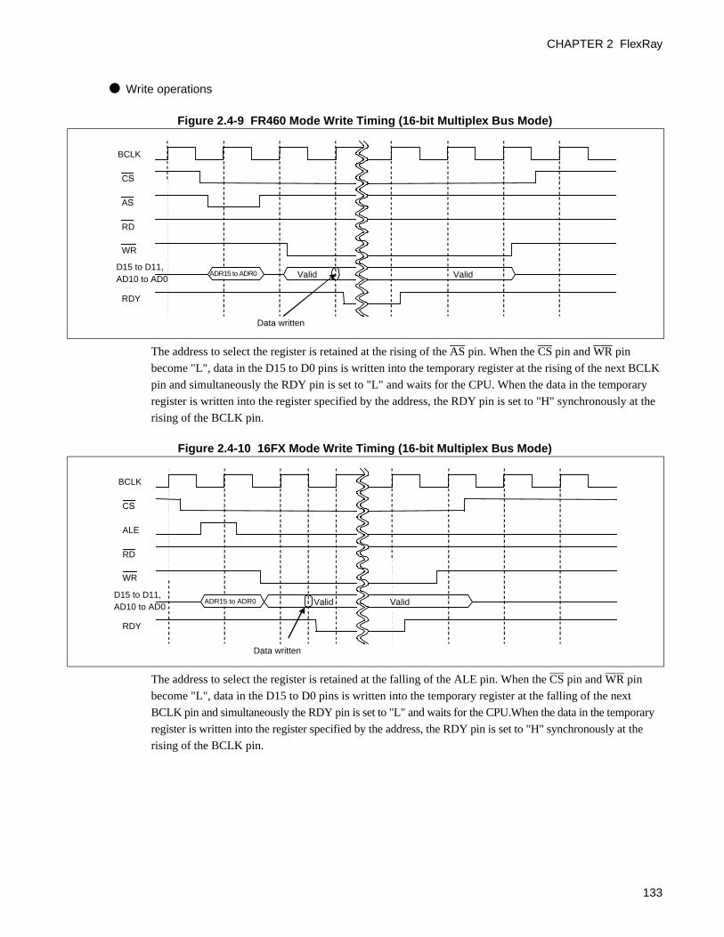
CHAPTER 2 FlexRay
● Write operations
Figure 2.4-9 FR460 Mode Write Timing (16-bit Multiplex Bus Mode)
The address to select the register is retained at the rising of the AS pin. When the CS pin and WR pin
become "L", data in the D15 to D0 pins is written into the temporary register at the rising of the next BCLK
pin and simultaneously the RDY pin is set to "L" and waits for the CPU. When the data in the temporary
register is written into the register specified by the address, the RDY pin is set to "H" synchronously at the
rising of the BCLK pin.
Figure 2.4-10 16FX Mode Write Timing (16-bit Multiplex Bus Mode)
The address to select the register is retained at the falling of the ALE pin. When the CS pin and WR pin
become "L", data in the D15 to D0 pins is written into the temporary register at the falling of the next
BCLK pin and simultaneously the RDY pin is set to "L" and waits for the CPU.When the data in the temporary
register is written into the register specified by the address, the RDY pin is set to "H" synchronously at the
rising of the BCLK pin.
BCLK
CS
RD
WR
AS
RDY
Valid Valid
Data written
ADR15 to ADR0D15 to D11,AD10 to AD0
BCLK
CS
RD
WR
ALE
RDY
Valid Valid
Data written
ADR15 to ADR0D15 to D11,AD10 to AD0
133
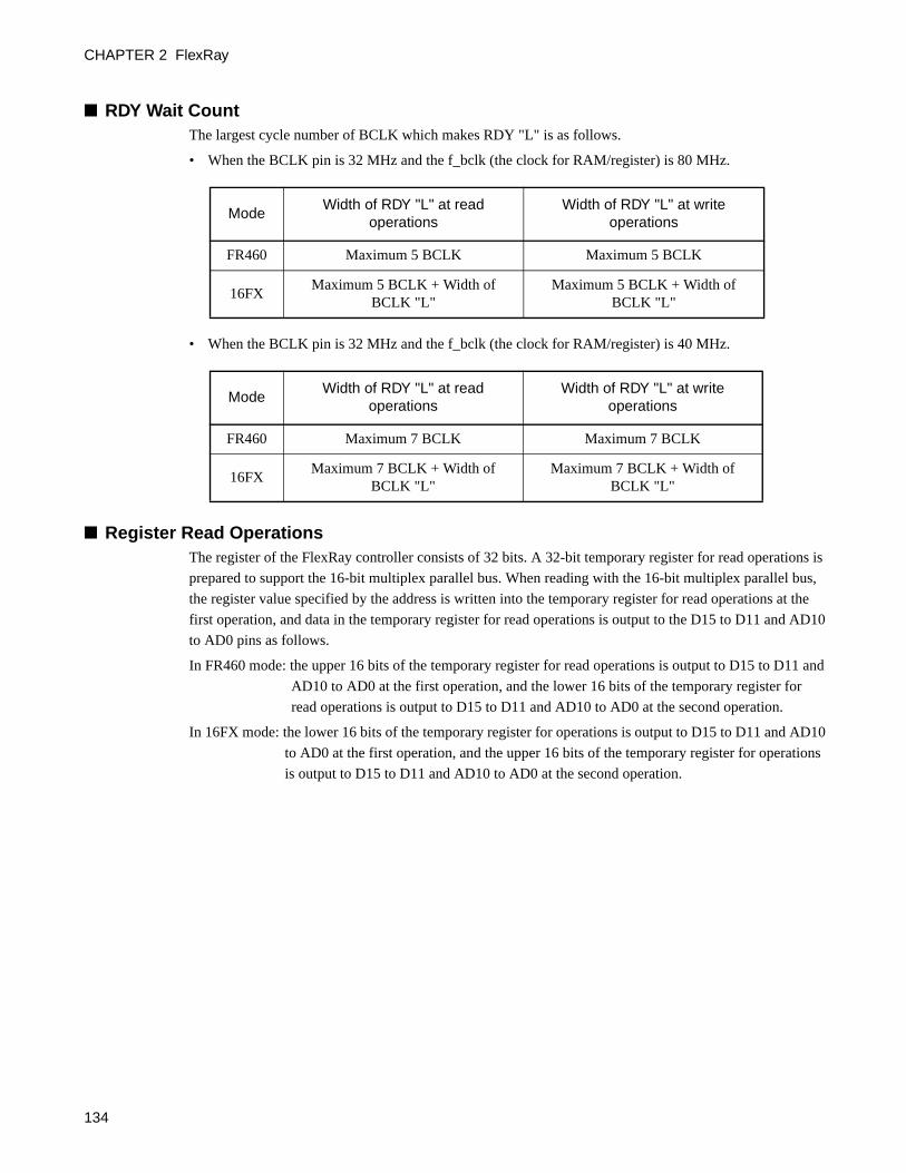
CHAPTER 2 FlexRay
■ RDY Wait CountThe largest cycle number of BCLK which makes RDY "L" is as follows.
• When the BCLK pin is 32 MHz and the f_bclk (the clock for RAM/register) is 80 MHz.
• When the BCLK pin is 32 MHz and the f_bclk (the clock for RAM/register) is 40 MHz.
■ Register Read OperationsThe register of the FlexRay controller consists of 32 bits. A 32-bit temporary register for read operations is
prepared to support the 16-bit multiplex parallel bus. When reading with the 16-bit multiplex parallel bus,
the register value specified by the address is written into the temporary register for read operations at the
first operation, and data in the temporary register for read operations is output to the D15 to D11 and AD10
to AD0 pins as follows.
In FR460 mode: the upper 16 bits of the temporary register for read operations is output to D15 to D11 and
AD10 to AD0 at the first operation, and the lower 16 bits of the temporary register for
read operations is output to D15 to D11 and AD10 to AD0 at the second operation.
In 16FX mode: the lower 16 bits of the temporary register for operations is output to D15 to D11 and AD10
to AD0 at the first operation, and the upper 16 bits of the temporary register for operations
is output to D15 to D11 and AD10 to AD0 at the second operation.
ModeWidth of RDY "L" at read
operationsWidth of RDY "L" at write
operations
FR460 Maximum 5 BCLK Maximum 5 BCLK
16FXMaximum 5 BCLK + Width of
BCLK "L" Maximum 5 BCLK + Width of
BCLK "L"
ModeWidth of RDY "L" at read
operationsWidth of RDY "L" at write
operations
FR460 Maximum 7 BCLK Maximum 7 BCLK
16FXMaximum 7 BCLK + Width of
BCLK "L" Maximum 7 BCLK + Width of
BCLK "L"
134
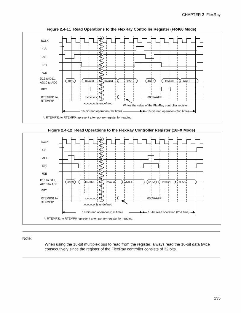
CHAPTER 2 FlexRay
Figure 2.4-11 Read Operations to the FlexRay Controller Register (FR460 Mode)
Figure 2.4-12 Read Operations to the FlexRay Controller Register (16FX Mode)
Note:
When using the 16-bit multiplex bus to read from the register, always read the 16-bit data twice consecutively since the register of the FlexRay controller consists of 32 bits.
BCLK
CS
RD
WR
RDY
RTEMP31 to RTEMP0*
*: RTEMP31 to RTEMP0 represent a temporary register for reading.
Invalid
xxxxxxxx
Invalid
0055AAFF
0055
AAFF
xxxxxxxx is undefined
16-bit read operation (1st time) 16-bit read operation (2nd time)
Invalid
AS
4n+2
Writes the value of the FlexRay controller register
D15 to D11,AD10 to AD0
4n+0
BCLK
CS
RD
WR
RDY
RTEMP31 to RTEMP0*
*: RTEMP31 to RTEMP0 represent a temporary register for reading.
InValid
xxxxxxxx
Invalid
0055AAFF
AAFF
0055
xxxxxxxx is undefined
16-bit read operation (1st time) 16-bit read operation (2nd time)
InValid
ALE
4n+2D15 to D11,AD10 to AD0
4n+0
135

CHAPTER 2 FlexRay
■ Register Write OperationsThe register of the FlexRay controller consists of 32 bits. A 32-bit temporary register for write operations is
prepared to support the 16-bit multiplex parallel bus.When writing with the 16-bit multiplex parallel bus,
the temporary register for write operations is written as follows.
In FR460 mode: data in D15 to D11 and AD10 to AD0 is written into the upper 16 bits of the temporary
register for write operations by the first operation, and data in D15 to D11 and AD10 to
AD0 is written into the lower 16 bits of the temporary register for write operations by the
second operation.
In 16FX mode: data in D15 to D11 and AD10 to AD0 is written into the lower 16 bits of the temporary
register for write operations by the first operation, and data in D15 to D11 and AD10 to
AD0 is written into the upper 16 bits of the temporary register for write operations by the
second operation.
Data in the temporary register is written into the register for the FlexRay controller at the second write
operation.
Figure 2.4-13 Write Operations to the FlexRay Controller Register (FR460 Mode)
BCLK
CS
RD
WR
RDY
WTEMP31 to WTEMP0 *
*: WTEMP31 to WTEMP0 represent a temporary register for writing.
0055
0055xxxx
AAFF
0055AAFF 0055AAFF
Writes to the FlexRay controller register
AAFF
xxxx is undefined
16-bit write operation (1st time) 16-bit write operation (2nd time)
AS
4n+2D15 to D11,AD10 to AD0
4n+0
136

CHAPTER 2 FlexRay
Figure 2.4-14 Write Operations to the FlexRay Controller Register (16FX Mode)
Note:
When using the 16-bit multiplex bus to write to the register, always write the 16-bit data twice consecutively since the register of the FlexRay controller consists of 32 bits.
BCLK
CS
RD
WR
RDY
WTEMP31 to WTEMP0 *
*: WTEMP31 to WTEMP0 represent a temporary register for writing.
0055
xxxx0055
AAFF
AAFF0055 AAFF0055
Writes to the FlexRay controller register
AAFF
xxxx is undefined
16-bit write operation (1st time) 16-bit write operation (2nd time)
AS
4n+0 4n+2D15 to D11,AD10 to AD0
137
CHAPTER 2 FlexRay
2.4.1 DMA Operations
This section explains the operation of the DMA.
■ DMA OperationsMB88121B supports the DMA transfer of input/output buffer data. When the host CPU is capable of a
DMA transfer using the external bus, connect the DMA_req pin of MB88121B to the DMA request input
pin of the host CPU.
138

CHAPTER 2 FlexRay
■ Input Buffer Data Transfer
Figure 2.4-15 Input Buffer Data Transfer
HOST: Initialize the MB88121B DMA Support RegisterDMAS.DMARE = 0; (Disable DMA requests)DMAS.DMAINV = 0; ("H" level active)DMAS.DMAOE = 1; (Enable the DMA_req pin output)
DMAS.DMARE = 1; (Enable DMA requests)
When the IBCM and IBCR register of the MB88121B are written to, the input buffer becomes active and the message buffer is transmitted
IBCM.LDSS = 1; (Update the data)IBCR.IBSYS = 0 ?If YES: IBCM.IBRH[6:0] = <Message Buffer> (begin transmission)DMAS.DMAOE = 0; (Disable DMA requests)
HOST: Initialize the host CPU
HOST: Enable the DMA_REQ line of the MB88121B
HOST: Execute the application (the DMA transfer runs in the background)
Is there transmit data for the input buffer?
HOST: Finish the DMA transfer, Send a message
HOST: Continue the application
Setup the DMA transferConfigure the data to write to the WRDSx registers (0400H to 04FCH) of the MB88121B via the external interface
The DMA_REQ signal becomes inactive and the output level is set to "L"
The DMA_REQ signal becomes active and the output level changes from "L" to "H"
The DMA_REQ signal becomes inactive and the output level changes from "H" to "L"
NO
YES
139

CHAPTER 2 FlexRay
■ Output Buffer Data Transfer
Figure 2.4-16 Output Buffer Data Transfer
The DMA_REQ signal becomes inactive and the output level is set to "L"
The DMA_REQ signal becomes active and the output level changes from "L" to "H"
The DMA_REQ signal becomes inactive and the output level changes from "H" to "L"
NO
NO
YES
YES
HOST: Copy the message data from the message RAM buffer to the shadow output buffer of the MB88121BOBCR.OBSYS == 0 ?; (Transfer in progress?) If YES:OBCR.OBRS[6:0] = <Message Buffer>;(The message buffer number is copied to the output buffer)OBCR.REQ = 1; Data transfer request (from message RAM to the shadow output buffer)
HOST: Initialize the MB88121B DMA Support RegisterDMAS.DMARE = 0; (Disable DMA requests), DMAS.DMAINV = 0; ("H" level active)DMAS.DMAOE = 1; (Enable the DMA_req pin output)
HOST: Initialize the DMA on the host CPU. Setup the DMA transfer. Configure the DMA to read data from the MB88121B output buffer (0600H to 06FCH) to memory via the external interface
HOST: Enable the DMA_REQ line of the MB88121BDMAS.DMARE = 1; (Enable DMA requests)
HOST: Finish the DMA transfer (message to host memory is received)
Are there other transfers from the output buffer?
HOST: Continue the application
DMAS.DMARE = 0; (Disable DMA requests)
HOST: Execute the application (the DMA transfer runs in the background)
HOST: Swap the MB88121B output buffer and shadow output buffer
Are there other transfers from the output buffer?
BOCR.OBSYS == 0 ?; (Transfer in progress?) If YES:OBCR.OBRS[6:0] = <Message Buffer>;(The message buffer number to copy to the output buffer)OBCR.REQ = 1;(Request a transfer from the message RAM to the shadow output buffer)
OBCR.OBSYS == 0 ? (Is there a transfer for the output buffer?)If YES; OBCR.VIEW = 1 (Swap)
140
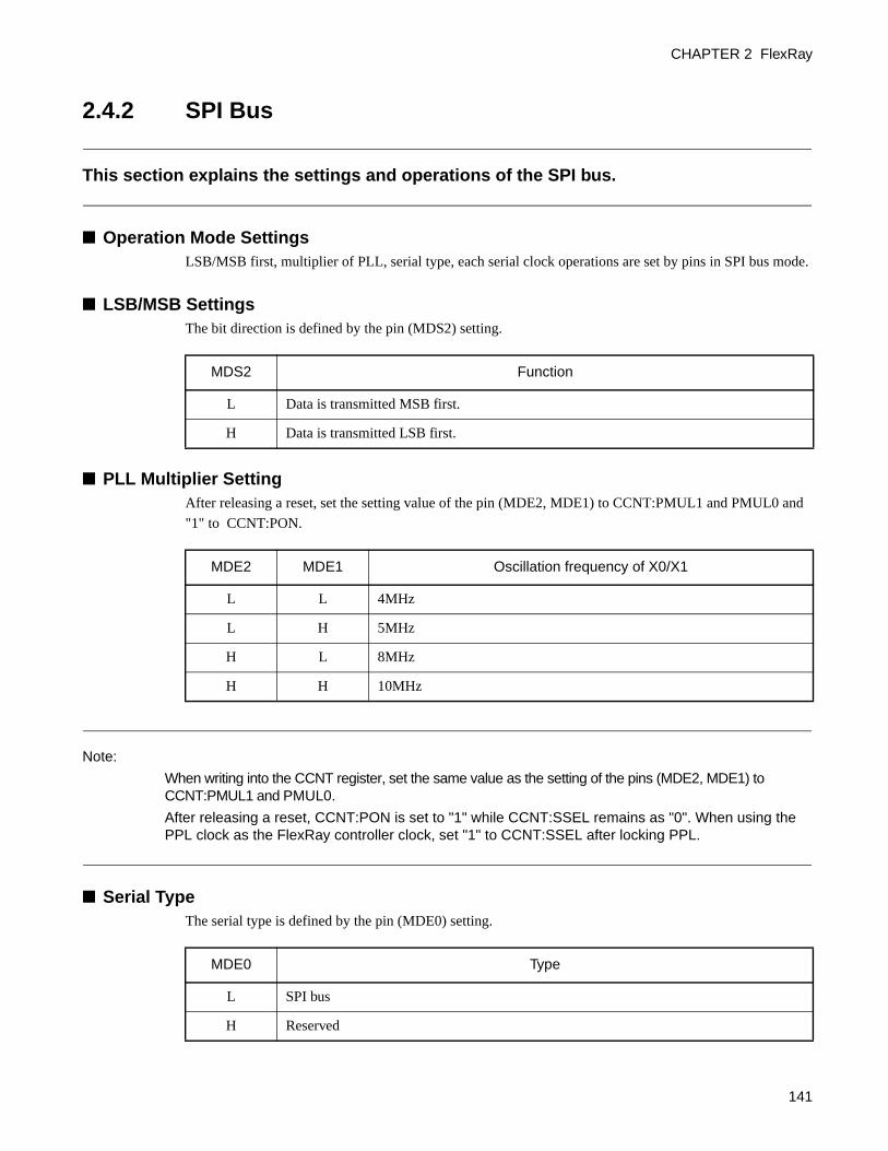
CHAPTER 2 FlexRay
2.4.2 SPI Bus
This section explains the settings and operations of the SPI bus.
■ Operation Mode SettingsLSB/MSB first, multiplier of PLL, serial type, each serial clock operations are set by pins in SPI bus mode.
■ LSB/MSB SettingsThe bit direction is defined by the pin (MDS2) setting.
■ PLL Multiplier SettingAfter releasing a reset, set the setting value of the pin (MDE2, MDE1) to CCNT:PMUL1 and PMUL0 and
"1" to CCNT:PON.
Note:
When writing into the CCNT register, set the same value as the setting of the pins (MDE2, MDE1) to CCNT:PMUL1 and PMUL0.
After releasing a reset, CCNT:PON is set to "1" while CCNT:SSEL remains as "0". When using the PPL clock as the FlexRay controller clock, set "1" to CCNT:SSEL after locking PPL.
■ Serial TypeThe serial type is defined by the pin (MDE0) setting.
MDS2 Function
L Data is transmitted MSB first.
H Data is transmitted LSB first.
MDE2 MDE1 Oscillation frequency of X0/X1
L L 4MHz
L H 5MHz
H L 8MHz
H H 10MHz
MDE0 Type
L SPI bus
H Reserved
141

CHAPTER 2 FlexRay
■ Serial Clock Operations Setting
The serial clock operations are defined by the pins (MDS1, MDS0) setting.
■ Serial Clock Operations4 types of serial clock operations are supported in the SPI bus mode. When the CS pin becomes "L", the pin
(SDO) becomes an output, fetches data from the pin (SDI) and outputs the data to the pin (SDO). When the
CS pin becomes "H", the pin (SDO) is in a high impedance state and data is invalid even if the serial clock
is entered to SCK.
■ MDS1 Pin = "L", MDS0 Pin ="L"SCK is "H" active and sampling is at the SCK rising edge. The following illustrates the operation timing.
Figure 2.4-17 Serial Clock Operation Timing when MDS1 Pin = "L" and MDS0 Pin = "L"
MDS1 MDS0 Serial clock operations
L L SCK is "H" active and sampling is at the SCK rising edge.
L H SCK is "H" active and sampling is at the SCK falling edge.
H L SCK is "L" active and sampling is at the SCK falling edge.
H H SCK is "L" active and sampling is at the SCK rising edge.
CS
SCK
SDI
SDO
Byte 1 Byte n
142

CHAPTER 2 FlexRay
■ MDS1 Pin = "L", MDS0 Pin ="H"SCK is "H" active and sampling is at the SCK falling edge. The following illustrates the operation timing.
Figure 2.4-18 Serial Clock Operation Timing when MDS1 Pin = "L" and MDS0 Pin = "H"
■ MDS1 Pin = "H", MDS0 Pin ="L"SCK is "L" active and sampling is at the SCK falling edge. The following illustrates the operation timing.
Figure 2.4-19 Serial Clock Operation Timing when MDS1 Pin = "H" and MDS0 Pin = "L"
■ MDS1 Pin = "H", MDS0 Pin ="H"SCK is "L" active and sampling is at the SCK rising edge. The following illustrates the operation timing.
Figure 2.4-20 Serial Clock Operation Timing when MDS1 Pin = "H" and MDS0 Pin = "H"
CS
SCK
SDI
SDO
Byte 1 Byte n
CS
SCK
SDI
SDO
Byte 1 Byte n
CS
SCK
SDI
SDO
Byte 1 Byte n
143

CHAPTER 2 FlexRay
2.5 SPI Protocol Definition
This section explains the commands of the SPI protocol definition.
■ SPI Protocol Definition SPI interface communications are performed by command frames. CS is negated to "H" between command
frames. A command frame consists of a command byte and an additional byte.
■ Command Byte Structure
* Bit 0 in the command byte is used as the address bit (A10) in the WR, RD commands. The bit is set to "0" for other commands.
Opcodes not included in the table are NOP commands.
P bit is the even numbered parity bit. The command becomes a NOP command in the event of a parity error.
bit 7 6 5 4 3 2 1 0
C4 C3 C2 C1 C0 "0" P *
C4=0:
Opcode C4 C3 C2 C1 C0 P Mnemonic Command
00H 0 0 0 0 0 0 NOP Read Status
0AH/09H 0 0 0 0 1 1/0 WR Write 1w
12H 0 0 0 1 0 1 WBI Initialize & Write Input Buffer
18H 0 0 0 1 1 0 WBC Write Input Buffer continuously
22H/21H 0 0 1 0 0 1/0 RD Read 1w
42H 0 1 0 0 0 1 RBI Initialize & Read Output Buffer
50H 0 1 0 1 0 0 RBIWBI Combination of RBI and WBI
5AH 0 1 0 1 1 1 RBIWBC Combination of RBI and WBC
60H 0 1 1 0 0 0 RBC Read Output Buffer continuously
72H 0 1 1 1 0 1 RBCWBI Combination of RBC and WBI
78H 0 1 1 1 1 0 RBCWBC Combination of RBC and WBC
C4=1:
Opcode C4 C3 C2 C1 C0 P Mnemonic Command
82H 1 0 0 0 0 1 WIP Write Input Buffer Pointer
88H 1 0 0 0 1 0 WOP Write Output Buffer Pointer
90H 1 0 0 1 0 0 WRIBC Write Input Buffer Command
9AH 1 0 0 1 1 1 WROBC Write Output Buffer Command
A0H 1 0 1 0 0 0 RDN Read nw
AAH 1 0 1 0 1 1 WRHSWrite Input Buffer Header
Section 1 to 3
144

CHAPTER 2 FlexRay
■ WR: 1w Write (0AH/09H)
ACK=FFH is transmitted if an error does not occur at the CRC_W check. ACK=00H is transmitted if an
error occurs. If ACK=FFH is transmitted, the 32-bit data in WD3 to WD0 is written into the address (A10
to A0) at the CS rising edge immediately after the ACK. The data is not written if an edge is not detected.
The SPI master can transmit an additional byte (Abort) after receiving the ACK. MB88121B does not write
data if it detects the clock edge at the CS rising.
Payload 4 bytes
Command length 10 bytes
Overhead 150%
Efficiency 40%
■ RRD: 1w Read (22H/21H)
Data RD3 to RD0 can be read from the address (A10 to A0). ACK=FFH is transmitted if an error does not
occur at the CRC_W check. ACK=00H is transmitted if an error occurs.
Payload 4 bytes
Command length 10 bytes
Overhead 50%
Efficiency 40%
■ WBI: Write Input Buffer, Initialize (12H)
*:A10 = bit 0 of the command byte, A9 to A2 = address byte, A1, A0 = 00B
SDI 09H/0AH Address* WD 0 WD 1 WD 2 WD 3 CRC_W Abort
SDO Status 0 Status 1 Status 0 CRC_R ACK
*:A10 = bit 0 of the command byte, A9 to A2 = address byte, A1, A0 = 00B
SDI 22H/21H Address* CRC_W
SDO Status 0 Status 1 Status 0 RD 0 RD 1 RD 2 RD 3 CRC_R ACK
*:n = Number of words - 1 (0 ≤ n ≤ 63)
SDI 12H n* WD 0 WD 4n+2 WD 4n+3 CRC_W Abort
SDO Status 0 Status 1 Status 2 CRC_R ACK
145
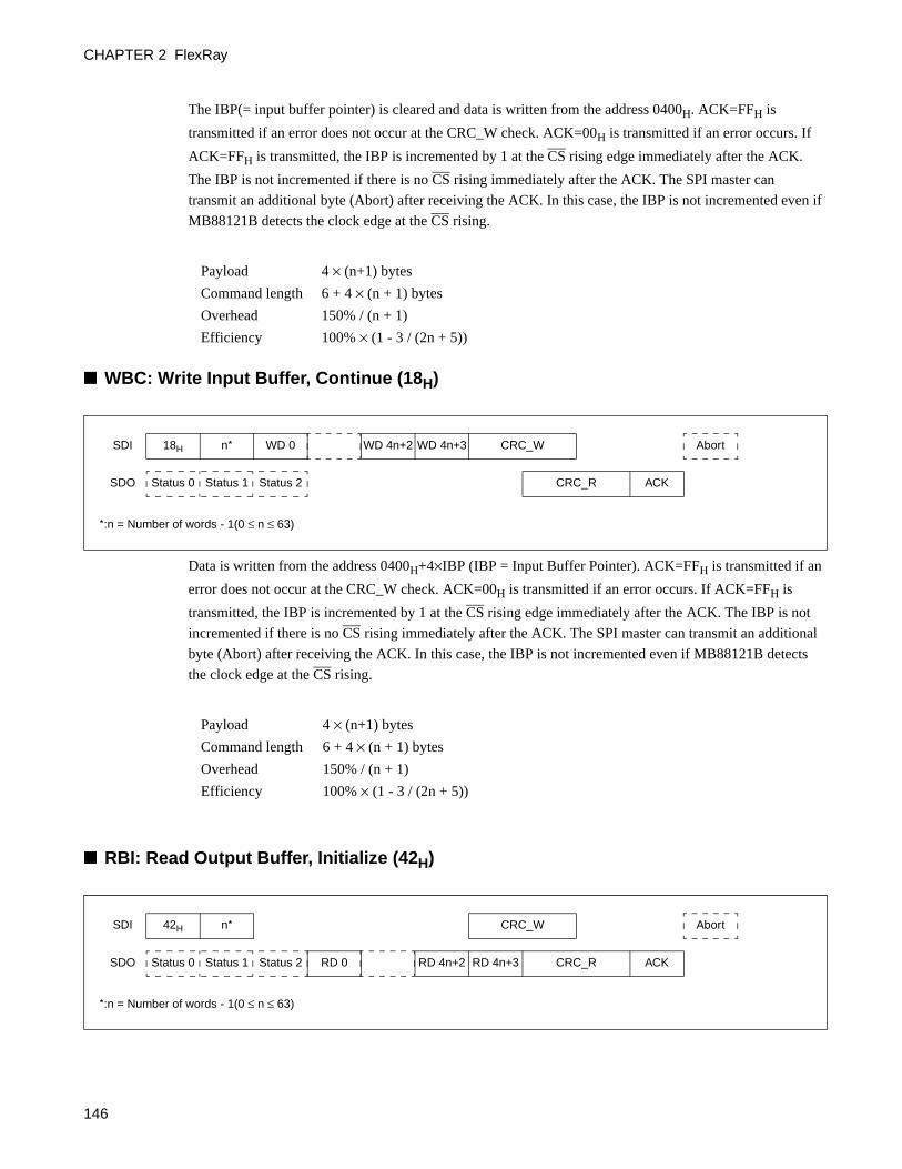
CHAPTER 2 FlexRay
The IBP(= input buffer pointer) is cleared and data is written from the address 0400H. ACK=FFH is
transmitted if an error does not occur at the CRC_W check. ACK=00H is transmitted if an error occurs. If
ACK=FFH is transmitted, the IBP is incremented by 1 at the CS rising edge immediately after the ACK.
The IBP is not incremented if there is no CS rising immediately after the ACK. The SPI master can
transmit an additional byte (Abort) after receiving the ACK. In this case, the IBP is not incremented even if
MB88121B detects the clock edge at the CS rising.
Payload 4 × (n+1) bytes
Command length 6 + 4 × (n + 1) bytes
Overhead 150% / (n + 1)
Efficiency 100% × (1 - 3 / (2n + 5))
■ WBC: Write Input Buffer, Continue (18H)
Data is written from the address 0400H+4×IBP (IBP = Input Buffer Pointer). ACK=FFH is transmitted if an
error does not occur at the CRC_W check. ACK=00H is transmitted if an error occurs. If ACK=FFH is
transmitted, the IBP is incremented by 1 at the CS rising edge immediately after the ACK. The IBP is not
incremented if there is no CS rising immediately after the ACK. The SPI master can transmit an additional
byte (Abort) after receiving the ACK. In this case, the IBP is not incremented even if MB88121B detects
the clock edge at the CS rising.
Payload 4 × (n+1) bytes
Command length 6 + 4 × (n + 1) bytes
Overhead 150% / (n + 1)
Efficiency 100% × (1 - 3 / (2n + 5))
■ RBI: Read Output Buffer, Initialize (42H)
*:n = Number of words - 1(0 ≤ n ≤ 63)
SDI 18H n* WD 0 WD 4n+2 WD 4n+3 CRC_W Abort
SDO Status 0 Status 1 Status 2 CRC_R ACK
*:n = Number of words - 1(0 ≤ n ≤ 63)
SDI 42H n* CRC_W Abort
SDO Status 0 Status 1 Status 2 RD 0 RD 4n+2 RD 4n+3 CRC_R ACK
146

CHAPTER 2 FlexRay
The OBP (= output buffer pointer) is cleared and data is read from the address (0600H). ACK=FFH is
transmitted if an error does not occur at the CRC_W check. ACK=00H is transmitted if an error occurs. If
ACK=FFH is transmitted, the OBP is incremented by 1 at the CS rising edge immediately after the ACK.
The OBP is not incremented if there is no CS rising immediately after the ACK. The SPI master can
transmit an additional byte (Abort) after receiving the ACK. In this case, the OBP is not incremented even
if MB88121B detects the clock edge at the CS rising.
Payload 4 × (n+1) bytes
Command length 6 + 4 × (n + 1) bytes
Overhead 150% / (n + 1)
Efficiency 100% × (1 - 3 / (2n + 5))
■ RBC: Read Output Buffer, Continue (60H)
Data is read from the address 0600H+4×OBP (OBP = Output Buffer Pointer). ACK=FFH is transmitted if
an error does not occur at the CRC_W check. ACK=00H is transmitted if an error occurs. If ACK=FFH is
transmitted, the OBP is incremented by 1 at the CS rising edge immediately after the ACK. The OBP is not
incremented if there is no CS rising immediately after the ACK. The SPI master can transmit an additional
byte (Abort) after receiving the ACK. In this case, the OBP is not incremented even if MB88121B detects
the clock edge at the CS rising.
Payload 4 × (n+1) bytes
Command length 6 + 4 × (n + 1) bytes
Overhead 150% / (n + 1)
Efficiency 100% × (1 - 3 / (2n + 5))
■ RBIWBI: Combination of RBI and WBI (50H)
The IBP(= input buffer pointer) is cleared and data is written from the address (0400H). Also, the OBP (=
output buffer pointer) is cleared and data is read from the address (0600H). ACK=FFH is transmitted if an
error does not occur at the CRC_W check. ACK=00H is transmitted if an error occurs. If ACK=FFH is
*:n = Number of words - 1(0 ≤ n ≤ 63)
SDI 60H n* CRC_W Abort
SDO Status 0 Status 1 Status 2 RD 0 RD 4n+2 RD 4n+3 CRC_R ACK
*:n = Number of words - 1(0 ≤ n ≤ 63)
SDI 50H n* WD 0 WD 4n+2 WD 4n+3 CRC_W Abort
SDO Status 0 Status 1 Status 2 RD 0 RD 4n+2 RD 4n+3 CRC_R ACK
147

CHAPTER 2 FlexRay
transmitted, the IBP and OBP are incremented by 1 at the CS rising edge immediately after the ACK. The
IBP and OBP are not incremented if there is no CS rising immediately after the ACK. The SPI master can
transmit an additional byte (Abort) after receiving the ACK. In this case, the IBP and OBP are not
incremented even if MB88121B detects the clock edge at the CS rising.
Payload 8 × (n+1) bytes
Command length 6 + 4 × (n + 1) bytes
Overhead 75% / (n + 1) - 50%
Efficiency 200% × (1 - 3 / (2n + 5))
■ RBCWBI: Combination of RBC and WBI (72H)
The IBP(= input buffer pointer) is cleared and data is written from the address (0400H). Also, data is read
from the address 0600H+4× OBP (OBP = Output Buffer Pointer). ACK=FFH is transmitted if an error does
not occur at the CRC_W check. ACK=00H is transmitted if an error occurs. If ACK=FFH is transmitted, the
IBP and OBP are incremented by 1 at the CS rising edge immediately after the ACK. The IBP and OBP are
not incremented if there is no CS rising immediately after the ACK. The SPI master can transmit an
additional byte (Abort) after receiving the ACK. In this case, the IBP and OBP are not incremented even if
MB88121B detects the clock edge at the CS rising.
Payload 8 × (n+1) bytes
Command length 6 + 4 × (n + 1) bytes
Overhead 75% / (n + 1) - 50%
Efficiency 200% × (1 - 3 / (2n + 5))
■ RBIWBC: Combination of RBI and WBC (5AH)
Data is written from the address 0400H+4×IBP (IBP = Input Buffer Pointer). Also, the OBP (= output
buffer pointer) is cleared and data is read from the address (0600H). ACK=FFH is transmitted if an error
does not occur at the CRC_W check. ACK=00H is transmitted if an error occurs. If ACK=FFH is
transmitted, the IBP and OBP are incremented by 1 at the CS rising edge immediately after the ACK. The
*:n = Number of words - 1(0 ≤ n ≤ 63)
SDI 72H n* WD 0 WD 4n+2 WD 4n+3 CRC_W Abort
SDO Status 0 Status 1 Status 2 RD 0 RD 4n+2 RD 4n+3 CRC_R ACK
*:n = Number of words - 1(0 ≤ n ≤ 63)
SDI 5AH n* WD 0 WD 4n+2 WD 4n+3 CRC_W Abort
SDO Status 0 Status 1 Status 2 RD 0 RD 4n+2 RD 4n+3 CRC_R ACK
148

CHAPTER 2 FlexRay
IBP and OBP are not incremented if there is no CS rising immediately after the ACK. The SPI master can
transmit an additional byte (Abort) after receiving the ACK. In this case, the IBP and OBP are not
incremented even if MB88121B detects the clock edge at the CS rising.
Payload 8 × (n+1) bytes
Command length 6 + 4 × (n + 1) bytes
Overhead 75% / (n + 1) - 50%
Efficiency 200% × (1 - 3 / (2n + 5))
■ RBCWBC: Combination of RBC and WBC (78H)
Data is written from the address 0400H+4×IBP (IBP = Input Buffer Pointer). Also, data is read from the
address 0600H+4×OBP (OBP = Output Buffer Pointer). ACK=FFH is transmitted if an error does not occur
at the CRC_W check. ACK=00H is transmitted if an error occurs. If ACK=FFH is transmitted, the IBP and
OBP are incremented by 1 at the CS rising edge immediately after the ACK. The IBP and OBP are not
incremented if there is no CS rising immediately after the ACK. The SPI master can transmit an additional
byte (Abort) after receiving the ACK. In this case, the IBP and OBP are not incremented even if
MB88121B detects the clock edge at the CS rising.
Payload 8 × (n+1) bytes
Command length 6 + 4 × (n + 1) bytes
Overhead 75% / (n + 1) - 50%
Efficiency 200% × (1 - 3 / (2n + 5))
■ WIP: Write Input Buffer Pointer (82H)
ACK=FFH is transmitted if an error does not occur at the CRC_W check. ACK=00H is transmitted if an
error occurs. If ACK=FFH is transmitted, the IBP is written to at the CS rising edge immediately after the
ACK. The IBP is not written to if there is no CS rising immediately after the ACK.
The SPI master can transmit an additional byte (Abort) after receiving the ACK. In this case, the IBP is not
written to even if MB88121B detects the clock edge at the CS rising.
The IBP is used by WBC, RBIWBC and RBCWBC commands.
*:n = Number of words - 1(0 ≤ n ≤ 63)
SDI 78H n* WD 0 WD 4n+2 WD 4n+3 CRC_W Abort
SDO Status 0 Status 1 Status 2 RD 0 RD 4n+2 RD 4n+3 CRC_R ACK
SDI 82H IBP CRC_W Abort
SDO Status 0 Status 1 Status 2 CRC_R ACK
149
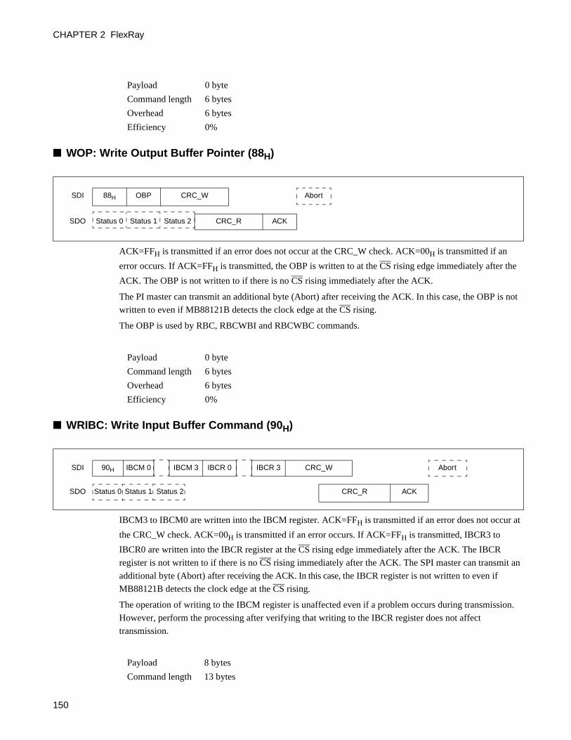
CHAPTER 2 FlexRay
Payload 0 byte
Command length 6 bytes
Overhead 6 bytes
Efficiency 0%
■ WOP: Write Output Buffer Pointer (88H)
ACK=FFH is transmitted if an error does not occur at the CRC_W check. ACK=00H is transmitted if an
error occurs. If ACK=FFH is transmitted, the OBP is written to at the CS rising edge immediately after the
ACK. The OBP is not written to if there is no CS rising immediately after the ACK.
The PI master can transmit an additional byte (Abort) after receiving the ACK. In this case, the OBP is not
written to even if MB88121B detects the clock edge at the CS rising.
The OBP is used by RBC, RBCWBI and RBCWBC commands.
Payload 0 byte
Command length 6 bytes
Overhead 6 bytes
Efficiency 0%
■ WRIBC: Write Input Buffer Command (90H)
IBCM3 to IBCM0 are written into the IBCM register. ACK=FFH is transmitted if an error does not occur at
the CRC_W check. ACK=00H is transmitted if an error occurs. If ACK=FFH is transmitted, IBCR3 to
IBCR0 are written into the IBCR register at the CS rising edge immediately after the ACK. The IBCR
register is not written to if there is no CS rising immediately after the ACK. The SPI master can transmit an
additional byte (Abort) after receiving the ACK. In this case, the IBCR register is not written to even if
MB88121B detects the clock edge at the CS rising.
The operation of writing to the IBCM register is unaffected even if a problem occurs during transmission.
However, perform the processing after verifying that writing to the IBCR register does not affect
transmission.
Payload 8 bytes
Command length 13 bytes
SDI 88H OBP CRC_W Abort
SDO Status 0 Status 1 Status 2 CRC_R ACK
SDI 90H IBCM 0 IBCM 3 IBCR 0 IBCR 3 CRC_W Abort
SDO Status 0 Status 1 Status 2 CRC_R ACK
150
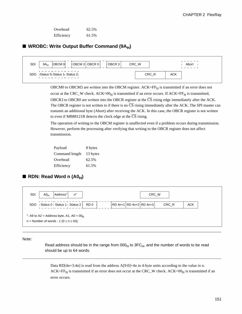
CHAPTER 2 FlexRay
Overhead 62.5%
Efficiency 61.5%
■ WROBC: Write Output Buffer Command (9AH)
OBCM0 to OBCM3 are written into the OBCM register. ACK=FFH is transmitted if an error does not
occur at the CRC_W check. ACK=00H is transmitted if an error occurs. If ACK=FFH is transmitted,
OBCR3 to OBCR0 are written into the OBCR register at the CS rising edge immediately after the ACK.
The OBCR register is not written to if there is no CS rising immediately after the ACK. The SPI master can
transmit an additional byte (Abort) after receiving the ACK. In this case, the OBCR register is not written
to even if MB88121B detects the clock edge at the CS rising.
The operation of writing to the OBCM register is unaffected even if a problem occurs during transmission.
However, perform the processing after verifying that writing to the OBCR register does not affect
transmission.
Payload 8 bytes
Command length 13 bytes
Overhead 62.5%
Efficiency 61.5%
■ RDN: Read Word n (A0H)
Note:
Read address should be in the range from 000H to 3FCH, and the number of words to be read should be up to 64 words.
Data RD[4n+3:4n] is read from the address A[9:0]+4n in 4-byte units according to the value in n.
ACK=FFH is transmitted if an error does not occur at the CRC_W check. ACK=00H is transmitted if an
error occurs.
SDI 9AH OBCM 0 OBCM 3 OBCR 0 OBCR 3 CRC_W Abort
SDO Status 0 Status 1 Status 2 CRC_R ACK
*: A9 to A2 = Address byte, A1, A0 = 00B
n = Number of words - 1 (0 ≤ n ≤ 63)
SDI A0H Address* n* CRC_W
SDO Status 0 Status 1 Status 2 RD 0 RD 4n+1 RD 4n+2 RD 4n+3 CRC_R ACK
151

CHAPTER 2 FlexRay
Payload 4 × (n+1) bytes
Command length 6 + 4 × (n + 1) bytes
Overhead 150% / (n + 1)
Efficiency 100% × (1 - 3 / (2n + 5))
■ WRHS: Write Input Buffer Header Section 1 to 3 (AAH)
WRHS13 to WRHS10 are written to the WRHS1 register, and WRHS23 to WRHS20 are written to the
WRHS2 register. ACK=FFH is transmitted if an error does not occur at the CRC_W check. ACK=00H is
transmitted if an error occurs. If ACK=FFH is transmitted, WRHS33 to WRHS30 is written into the
WRHS3 register at the CS rising edge immediately after the ACK. The WRHS3 register is not written to if
there is no CS rising immediately after the ACK. The SPI master can transmit an additional byte (Abort)
after receiving the ACK. In this case, the WRHS3 register is not written to even if MB88121B detects the
clock edge at the CS rising.
The operation of writing to the WRHS1 and WRHS2 registers is unaffected even if a problem occurs
during transmission.
Payload 12 bytes
Command length 17 bytes
Overhead 41.7%
Efficiency 70.6%
■ NOP: Read Status (00H)
Payload 0 byte
Command length 6 bytes
Overhead 6 bytes
Efficiency 0%
SDI AAH WRHS10 WRHS13 WRHS20 WRHS33 CRC_W Abort
SDO Status 0 Status 1 Status2 CRC_R ACK
SDI 00H - CRC_W
SDO Status 0 Status 1 Status 2 CRC_R ACK
152

CHAPTER 2 FlexRay
2.5.1 Data Security Algorithm
This section explains the data security algorithm.
■ Data Security AlgorithmCRC_x: CRC_W and CRC_R fields are used for error detection. The CRC consists of 16 bits. The initial
value is 0x1d0f and CRC polynomial is 0x1021 (X12+X5+1) when the field is generated.
Example:
WR command:
1. 0x0a (Command)
2. 0x04 (Address)
3. 0x0F (WD0)
4. 0x00 (WD1)
5. 0x00 (WD2)
6. 0x00 (WD3)
7. CRC_W
8. CRC_W
9. 0xFF (Fill Byte)
10. 0xFF (Fill Byte)
Bytes 1 to 6 must be used for CRC_W calculation.
Fill byte indicates arbitrary value (e.g. 0xFF, 0x00).
RD command:
1. 0x21 (Command)
2. 0x00 (Address)
3. 0xFF (Fill Byte)
4. 0xFF (Fill Byte)
5. 0xFF (Fill Byte)
6. 0xFF (Fill Byte)
7. CRC_W
8. CRC_W
9. 0xFF (Fill Byte)
10. 0xFF (Fill Byte)
Bytes 1, 2 must be used for CRC_W calculation of RD command.
Fill byte indicates arbitrary value (e.g. 0xFF, 0x00).
Note:
CRC must be generated as data of MSB first. Note that CRC is used in the LSB first mode.
153

CHAPTER 2 FlexRay
ACK: The ACK field consists of 8 bits. MB88121B notifies the host whether or not the CRC check on
the received CRC_W field has been successful using the ACK field. ACK=FFH is transmitted
when successful, and ACK=00H is transmitted for an error.
The host can correct the error from cs (ACK) that adds each bits in the ACK field as shown in
the following expression.
For example, the error correction on an acknowledge ACK_ecc is as follows.
If cs(ACK) ≥ 6, ACC_ecc is "OK". In this case, the host determines that the transmission has
been successful.
If cs(ACK) ≤ 5, ACC_ecc is "NG". In this case, the host transmits the additional byte (abort
command). Set CS to "H" and restart the transmission.
Abort: After receiving the correct CRC_W, the MB88121B performs the appropriate processing
(writing to a register or updating the IBP/OBP) on the rising edge of the CS signal following the
ACK byte (however, data is written into the input buffer as each word is read).
MB88121B does not perform an action if there is no CS rising, or on the other timings.
The host cannot determine if MB88121B has received the message correctly if any bits are
missing from the ACK byte. In this case, the host can transmit an Abort (interpreted by
MB88121B) as an additional byte at the CS timing. In such a case, the message is ignored and
writing to the register or updating the IBP/OBP does not occur.
Example) Transmit Abort by WR command
DMY: Additonal byte. The DMY value is arbitrarily. When the additional byte is added, the DMY is
handled as Abort.
cs ACK( ) ACK i[ ]i 0=∑=7
SDI 0AH Address WD0 WD1 WD2 WD3 CRC_W FFH FFH DMY
CS
154

CHAPTER 2 FlexRay
2.5.2 SPI Status Output
This section explains the SPI status output.
■ SPI Status OutputIn the SPI interface protocol, the first 3 bytes in the command frame are status information.
● Status 0
This register indicates the status of the input buffer and output buffer. The status is updated at the falling
edge of CS.
bit 7 6 5 4 3 2 1 0
0 0 0 0 0 0 STO1 STO0
Bit Bit name Description
7 - "0"
6 - "0"
5 - "0"
4 - "0"
3 - "0"
2 - "0"
1 STO1
OBSYSWhen this bit is "1", the output buffer is in use. Also, writing into the OBCR register is not available. When this bit is set to "1" by the WROBC command, the command does not write into the OBCM and OBCR registers.
0 STO0
IBSYHWhen this bit is "1", the input buffer is in use. Writing into the input buffer is not available. When this bit is set to "1" by the WRIBC command, the command does not write into the IBCM and IBCR registers.
155

CHAPTER 2 FlexRay
● Status 1
This register indicates the status of the previous SPI command. This status is cleared by hardware_reset.
bit 7 6 5 4 3 2 1 0
ST17 ST16 0 ST14 ST13 ST12 ST11 ST10
Bit Bit name Description
7 ST17Command parity error"1": Error"0": No error
6 ST16
Command format error (Example: bit 2/bit 0 of the command is "1", except for A10 bit)"1": Error"0": No error
5 - "0"
4 ST14Undefined command (when C4 to C0=05H to 07H, 09H, 0DH, 16H to 1FH) error
3 ST13
Eray busy error (Example: The CPU has attempted to write data into the input buffer or IBCM/IBCR register while the input buffer is busy. Or, the CPU has attempted to write data into the OBCM/OBCR register while the output buffer is busy. In such cases, an access error occurs and data is not written.)"1": Error"0": No error
2 ST12Long message error"1" : Receive the long message."0" : Receive the specified message or short message.
1 ST11Short message error"1" : Receive the short message."0" : Receive the specified message or long message.
0 ST10CRC error"1": Error"0": No error
156

CHAPTER 2 FlexRay
● Status 2
This register indicates the status of the interrupt request. The status is changed at the falling edge of CS.
bit 7 6 5 4 3 2 1 0
0 0 ST25 ST24 ST23 ST22 ST21 ST20
Bit Bit name Description
7 - "0"
6 - "0"
5 ST25Timer 1 interrupt pin flag"1": Output "H" to timer 1 interrupt pin."0": Output "L" to timer 1 interrupt pin.
4 ST24Timer 0 interrupt pin flag"1": Output "H" to timer 0 interrupt pin."0": Output "L" to timer 0 interrupt pin.
3 ST23Interrupt 1 pin flag"1": Output "H" to interrupt 1 pin."0": Output "L" to interrupt 1 pin.
2 ST22Interrupt 0 pin flag"1": Output "H" to interrupt 0 pin."0": Output "L" to interrupt 0 pin.
1 ST21Status interrupt flag"1": Set any of the bits in the status interrupt register to "1"."0": Set all bits of the status interrupt register to "0".
0 ST20Error interrupt flag"1": Set any of the bits in the error interrupt register to "1"."0": Set all bits of the error interrupt register to "0".
157

CHAPTER 2 FlexRay
2.6 FlexRay Controller Clock
This section explains the FlexRay controller clock.
■ FlexRay Controller Clock Figure 2.6-1 illustrates the clock distribution diagram in non-multiplex bus mode and multiplex bus mode,
and Figure 2.6-2 illustrates the clock distribution diagram in SPI bus mode. The following describes each
clock (sclk, f_bclk and f_sclk).
• sclk : System clock
• f_bclk : RAM/register clock
• f_sclk : FlexRay operation clock (FlexRay sample clock)
Figure 2.6-1 Clock Distribution Diagram in Non-multiplex Bus Mode and Multiplex Bus Mode
Clock generation
circuit
00
10
x1
PLL 0
1
00
01
10
11
CPU Interface
CCNT:SDIV1,SDIV0
CCNT.RCLK
1/2 frequency
divider
1/2 frequency
divider
1/4 frequency
divider
1/8 frequency
divider
f_bclk
f_sclk
sclk
(CCNT.SSEL, CCNT.STOP)
FlexRay Controller
CCNT:PMUL1,PMUL0
CCNT.PON
X0
X1
Sel
ecto
r
Selector
Selector
158
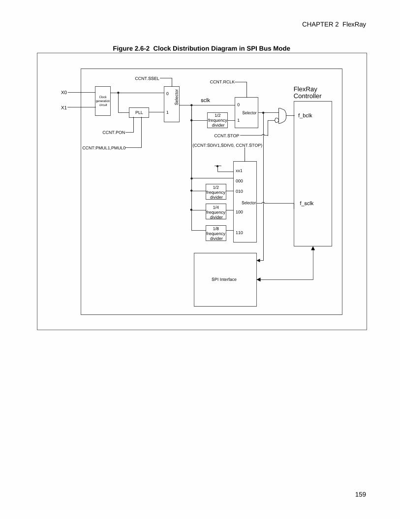
CHAPTER 2 FlexRay
Figure 2.6-2 Clock Distribution Diagram in SPI Bus Mode
0
1PLL
0
1
xx1
000
010
100
110
(CCNT:SDIV1,SDIV0, CCNT.STOP)
CCNT.RCLK
f_bclk
f_sclk
sclk
CCNT.SSEL
CCNT:PMUL1,PMUL0
CCNT.PON
X0
X1
CCNT.STOP
Clock generation
circuit
SPI Interface
1/2 frequency
divider
1/2 frequency
divider
1/4 frequency
divider
1/8 frequency
divider
FlexRay Controller
Sel
ecto
r
Selector
Selector
159

CHAPTER 2 FlexRay
2.6.1 FlexRay Controller Clock Control Procedure
This section explains the FlexRay controller clock control reference.
■ Switching Procedure to the PLL ClockWhen switching from the reference clock (X0/X1) to the PLL clock, follow the procedure below to
configure PLL before switching.
1. Configure multipliers to CCNT:PMUL1 and PMUL0 to adjust the PLL clock to 80 MHz.
2. Set CCNT:PON=1.
3. Set CCNT:SSEL=1 after the lockup time (600µs) has elapsed.
Note:
The update is possible only when CCSV:POCS5 to POCS0 is in the DEFAULT_CONFIG state or CONFIG state.
■ Switching Procedure to the Reference ClockFollow the procedure below when switching from the PLL clock to the reference clock (X0/X1),
1. Set CCNT:SSEL=0.
2. Set CCNT:PON=0 to stop PLL.
Note:
The update is possible only when CCSV:POCS5 to POCS0 is in the DEFAULT_CONFIG state or CONFIG state.
■ Switching Procedure to Stop ModeFollow the procedure below when switching to stop mode.
• Set CCNT:STOP=1.
Follow the procedure below when stopping the oscillation of PPL and switching to stop mode .
1. Set CCNT:SSEL=0.
2. Set CCNT:PON=0.
3. Set CCNT:STOP=1.
Note:
The update is possible only when CCSV:POCS5 to POCS0 is in the DEFAULT_CONFIG state or CONFIG state.
160
CHAPTER 2 FlexRay
■ Restoration Procedure from Stop ModeFollow the procedure below when restoring from stop mode.
• Set CCNT:STOP=0.
■ Switching the System Clock Divider Value Change the system clock divider value (CCNT:SDIV1 and SDIV0) when selecting the reference clock.
Note:
The update is possible only when CCSV:POCS5 to POCS0 is in the DEFAULT_CONFIG state or CONFIG state.
■ RAM Clock ConfigurationChange CCNT:RCLK to switch the RAM clock when selecting the reference clock to switch the RAM
clock.
Note:
The update is possible only when CCSV:POCS5 to POCS0 is in the DEFAULT_CONFIG state or CONFIG state.
161

CHAPTER 2 FlexRay
2.6.2 Setting Example of the FlexRay Baud Rate
This section explains the setting example of the FlexRay baud rate.
■ Setting Example of the FlexRay Baud Rate
The following examples describe baud rate settings on each FlexRay sample clock f_sclk* using values
defined by PRTC1:BRP1 and BRP0.
1 bit time always consists of 8 samples. The sample clock f_sclk is configured by CCNT:SDIV1 and
SDIV0.
● When f_sclk = 80MHz
BRP1, BRP0 =00B (default): Baud rate = 10 Mbps
gdSampleClockPeriod = 1/f_sclk = 12.5 ns
pSamplesPerMicrotick = 2 (1µT = 25 ns)
BRP1, BRP0 =01B: Baud rate = 5 Mbps
gdSampleClockPeriod = 2/f_sclk = 25 ns
pSamplesPerMicrotick = 1 (1µT = 25 ns)
BRP1, BRP0 =10B, 11B: Baud rate = 2.5 Mbps
gdSampleClockPeriod = 4/f_sclk = 50 ns
pSamplesPerMicrotick = 1 (1µT = 50 ns)
● When f_sclk = 40MHz
BRP1, BRP0 =00B (default): Baud rate = 5 Mbps
gdSampleClockPeriod = 1/f_sclk = 25 ns
pSamplesPerMicrotick = 2 (1µT = 50 ns)
BRP1, BRP0 =01B: Baud rate = 2.5 Mbps
gdSampleClockPeriod = 2/f_sclk = 50 ns
pSamplesPerMicrotick = 1 (1µT = 50 ns)
BRP1, BRP0 =10B, 11B: Baud rate = 1.25 Mbps
gdSampleClockPeriod = 4/f_sclk = 100 ns
pSamplesPerMicrotick = 1 (1µT = 100 ns)
162
CHAPTER 2 FlexRay
2.7 FlexRay Protocol Function
This section explains the FlexRay protocol function.
■ FlexRay Protocol Function This section explains FlexRay protocol function. See "the FlexRay Protocol Specifications V2.1" for
further details on the FlexRay protocol.
163

CHAPTER 2 FlexRay
2.7.1 Communication Cycle
This section explains the functions and settings of the communication cycle.
■ Communication CycleThe FlexRay communication cycle consists of the following elements.
• Static segment
• Dynamic segment (optional)
• Symbol window (optional)
• Network idle time (NIT)
The network communication time (NCT) consists of static segment, dynamic segment and symbol window.
The slot counter starts at "1" on each communication ch. and counts until the end of the dynamic
segment.Also, both channels use synchronized identical macroticks.
Figure 2.7-1 Communication Cycle Structure
■ Static SegmentThe static segment has the following features.
• The slot is (available) protected by the bus guardian.
• The frame transmission starts at the action point of each static slot.
• The payload length is the same among all frames on both channels.
Parameter: Number of static slots GTUC7:NSS9 to NSS0
Static slot length GTUC7:SSL9 to SSL0
Static frame data length MHDC:SFDL6 to SFDL0
Action point offset GTUC9:APO5 to APO0
time basederived trigger
t
NITSymbol window
Static segment
Dynamic segment
Communication cycle x-1 Communication cycle x Communication cycle x+1
time basederived trigger
164
CHAPTER 2 FlexRay
■ Dynamic Segment The dynamic segment has the following features.
• All controllers have bus access, and (available) the bus guardian is not valid.
• The slot length is variable and different between both channels.
• The transmission starts at the mini slot action point.
Parameter: Number of mini slots GTUC8:NMS12 to NMS0
Mini slot length GTUC8:MSL5 to MSL0
Mini slot action point offset GTUC9:MAPO4 to MAPO0
Transmission complete mini slot value MHDC:SLT12 to SLT0
■ Symbol Window The FlexRay Protocol Specifications V2.1 defines 3 symbols.
• Wakeup symbol (WUS) is only transmitted in the WAKEUP state.
• Collision avoidance symbol (CAS) is only transmitted in the STARTUP state.
• Media access test symbol (MTS) is transmitted in the NORMAL_ACTIVE state to test the bus guardian.
1 MTS symbol per channel is transmitted during the symbol window period.
The symbol window has the following features.
• Transmits 1 symbol.
• The transmission of MTS symbol starts at the symbol window action point.
Parameter: Action point offset GTUC9:APO5 to APO0
Network idle time start GTUC4:NIT13 to NIT0
■ Network Idle Time (NIT)The FlexRay controller performs the following tasks during the network idle time (NIT).
• Calculates the clock correction time (offset and rate).
• Starts and performs the offset correction on each macrotick.
• Performs tasks associated with the cluster cycle.
Parameter: Network idle time start GTUC4:NIT13 to NIT0
Offset correction start GTUC4:OCS13 to OCS0
165

CHAPTER 2 FlexRay
■ Starting NIT and Configuring the Offset Correction Start
Figure 2.7-2 Starting NIT and Configuring the Offset Correction Start
Assuming the number of microticks per cycle as m, configure as GTUC2:MPC = m. Also, assume that static/dynamic segment starts at macrotick 0 and ends at macrotick n.
n = Static segment length + dynamic segment offset + dynamic segment length - 1MT
The static segment length should be configured in GTUC7:SSL9 to SSL0 and GTUC7:NSS9 to NSS0.
The dynamic segment length should be configured in GTUC8:MSL5 to MSL0 and GTUC8:NMS12 to NMS0.
The dynamic segment offset can be calculated as below.
if gdActionPointOffset ≤ gdMinislotActionPointOffset :
Dynamic segment offset = 0 MT
if gdActionPointOffset > gdMinislotActionPointOffset :
Dynamic segment offset = gdActionPointOffset - gdMinislotActionPointOffset
Configure as follows when NIT starts at macrotick k+1 and ends at the last macrotick of the m-1 cycle.
GTUC4:NIT = k
Also, configure offset correction start to satisfy the following condition.
GTUC4:OCS ≥ GTUC4:NIT + 1 = k+1
The symbol window length between the end of the static/dynamic segment and the beginning of NIT is calculated as k-n.
0 n n+1 k k+1 m-1GTUC2, MPC13 to MPC0 = m
GTUC4, NIT13 to NIT0= k
GTUC4, OCS13 to OCS0 = NIT + 1Static / dynamic segment
Symbol window NIT
166

CHAPTER 2 FlexRay
2.7.2 Communication Mode
This section explains the functions of the communication mode.
■ Communication ModeThe FlexRay protocol V2.1 supports time-triggered distributed (TT-D) mode. This section explains time
triggered distributed (TT-D) communication mode.
■ Time-triggered Distributed (TT-D)The following communication modes are available within TT-D mode.
• Pure static : Minimum 2 static slots + symbol window (optional)
• Mixed static/dynamic : Minimum 2 static slots + dynamic segment + symbol window (optional)
Time-triggered distributed mode operation requires a minimum of 2 cold start nodes. Also, the cluster
startup requires 2 faultless cold start nodes. The startup frames should be sync frames. All cold start nodes
become synchronized nodes.
167

CHAPTER 2 FlexRay
2.7.3 Clock Synchronization
This section explains the clock synchronization.
■ Clock SynchronizationTT-D mode uses distributed clock synchronization. Each node synchronizes itself to the cluster by
measuring the receive timing of sync frames from other nodes.
■ Global TimeAlthough each node has its own clock, these all operate on the concept of global time. The global time
consists of a vector of 2 values, namely the cycle (cycle counter) and cycle time (macrotick counter).
• Macrotick (MT) = The base unit of the FlexRay network time measurement. (Macrotick is a multiple of microticks (µT) (only by an integer))
• Cycle = The unit to represent the duration of 1 communication cycle(Cycles are expressed by macroticks (MT))
■ Local TimeThe node operation time is regulated in microtick units internally to the node. A microtick is a controller
specific time unit obtained from the oscillation clock of each node. Therefore, even if the node is the same,
if the controllers are different then the time needs to be set and maintained separately. The accuracy of
these local time errors is measured by microtick units (µT).
• Microtick generation order: Oscillation clock to prescaler to microtick (µT)
• µT = The base unit of measuring time in the FlexRay controller (clock correction is carried out in µT units)
• Cycle counter + macrotick counter = The local view of the node's global time
■ Synchronization ProcessSync frames are used for clock synchronization. Only previously configured synchronization nodes are able
to transmit sync frames. For a 2 channel cluster, the synchronization node should transmit sync frames to
both channels.
There are the following restriction in synchronization in FlexRay.
• A maximum of 1 sync frame per node per communication cycle.
• A maximum of 15 sync frames per cluster per communication cycle.
• Use the previously configured number of sync frames (GTUC2:SNM3 to SNM0) on all nodes for clock synchronization.
• A minimum of 2 synchronization nodes are required for clock synchronization and startup.
The time deviation between the expected sync frame receive time and observed receive time during the
static segment period are measured for clock synchronization. The calculation for correction time is
performed during NIT (offset: all cycles, rate: odd number cycles) using the FTM algorithm. See "the
FlexRay Protocol Specifications V2.1 chapter 8" for details.
168

CHAPTER 2 FlexRay
■ Offset (Phase) Correction • Deviation of the current cycle time is measured.
• For nodes with 2 channels, the smaller value measured among these channels is used for the calculation.
• This is calculated for NIT periods of all communication cycles.
• The offset correction value calculated with even number cycles is used only for checking errors.
• The error check is carried out by comparing against the limit value.
• The correction value is an integer with a sign in µT units.
• The correction is carried out on odd number cycles. The offset correction is distributed over each macrotick from the start till the end of the cycle (till the end of NIT), by lengthening or shortening the current cycle by a few MTs by shifting the next cycle start position.
■ Rate (Frequency) Correction• The difference in deviation of time is measured for even number cycles and odd number cycles.
• For nodes with 2 channels, the average deviation time differences measured among these channels are used for the calculation.
• This is calculated for NIT periods of odd number communication cycles.
• The cluster drift damping is carried out using the global damping value.
• The error check is carried out by comparing against the limit value.
• The correction value is a signed integer in µT units.
• The correction is carried out on the next even/odd number cycle pair. The correction is distributed over microticks forming 1 cycle, by lengthening or shortening the current cycle by a few µTs by shifting the next cycle pair starting position on each node.
■ Sync Frame TransmissionSync frames can be transmitted only from the buffer 0 or 1. The message buffer 1 is used to transmit sync
frames when the sync frame has different payloads on 2 channels. In this case, set MRC:SPLM bit to "1".
The message buffer to transmit sync frames must be structured with key slot IDs. This can be configured
only in DEFAULT_CONFIG state or CONFIG state.
Set SUCC1:TXSY to "1" on nodes which transmit sync frames.
■ External Clock SynchronizationA significant drift may occur in independent clusters during normal operations. When a synchronization
operation is required within an independent cluster, synchronize to an external clock.
• External offset/rate correction values are signed integers.
• External offset/rate correction values are added to the calculated offset/rate correction values.
• The total offset/rate correction time (external and internal) are checked against the configured limit value.
169

CHAPTER 2 FlexRay
2.7.4 Error Handling
This section explains the functions of the error handlings.
■ Error HandlingError handling deployed in FlexRay assumes that communications among unaffected nodes are guaranteed
while a lower layer protocol error is occurring among certain nodes. Implement an operation to restart
normal operations of the FlexRay controller within application programs. EIR:PEMC is set to "1" when a
transition to the error handling state occurs. Also, an interrupt occurs if an interrupt is valid. The actual error
mode is displayed by CCEV:ERRM1 and ERRM0.
■ Clock Correction Failed CounterA transition from the NORMAL_ACTIVE state to NORMAL_PASSIVE state occurs when the clock
correction failed counter has reached the Maximum Without Clock Correction Passive SUCC3: WCP3 to
WCP0. Also, a transition from NORMAL_PASSIVE state to HALT state occurs when the clock correction
failed counter has reached the Maximum Without Clock Correction Fatal SUCC3:WCF3 to WCF0.
The clock correction failed counter CCEV:CCFC3 to CCFC0 monitors the duration where a node's clock
correction time cannot be calculated after passing the startup phase. The clock correction failed counter is
incremented at the end of odd number communication cycles if either the Missing Offset Correction Signal
SFS:MOCS or Missing Rate Correction Signal SFS:MRCS is set to "1".
Table 2.7-1 POC Error Modes
Error mode Operation
ACTIVE(green)
Full operation State: NORMAL_ACTIVE
The FlexRay controller is completely synchronized and supporting the clock synchronization for the entire clusters. The error status and status transition information can be obtained by reading the error interrupt flag and status interrupt flag from the EIR register and SIR register. An interrupt occurs if an interrupt is valid.
PASSIVE(yellow)
Limited operationState: NORMAL_PASSIVE, FlexRay controller self recovery possible
The FlexRay controller stops transmitting frames and symbols, but is able to process received frames. The clock synchronization continues using receive frames, but an active clock synchronization among the entire cluster is not performed.The error status and status transition information can be obtained by reading the error interrupt flag and status interrupt flag from the EIR register and SIR register. An interrupt occurs if an interrupt is valid.
COMM_HALT(red)
Operation haltedState: HALT, FlexRay controller self recovery impossible
The FlexRay controller stops frame and symbol processing, clock synchronization processing and macrotick generation. The error status and status transition information can be obtained by reading the error interrupt flag and status interrupt flag from the EIR register and SIR register. The bus driver stops.
170

CHAPTER 2 FlexRay
The clock correction failed counter is set to "0" at the end of odd number communication cycles if Missing
Offset Correction Signal SFS:MOCS and Missing Rate Correction Signal SFS:MRCS are not set to "1".
The clock correction failed counter stops incrementing when it reaches the Maximum Without Clock
Correction Fatal SUCC3:WCF3 to WCF0 (therefore, the counter does not return to "0" by incrementing it
after reaching its maximum value). The clock correction failed counter is set to "0" at a transition from the
CONFIG state to the READY state or NORMAL_ACTIVE state.
■ Required Cycle Pair Counter for Status Transition between Passive and ActiveThe required cycle pair counter for status transition between Passive and Active, SUCC1:PTAC4 to PTAC0,
controls the POC transition from the NORMAL_PASSIVE state to NORMAL_ACTIVE state.
SUCC1:PTA4 to PTA0 defines the number of even/odd cycle pairs whose clock correction time is valid
before the transition from the NORMAL_PASSIVE state to NORMAL_ACTIVE state. The transition from
the NORMAL_PASSIVE state to NORMAL_ACTIVE state is not allowed if SUCC1:PTA4 to PTA0 are
set to "0".
■ HALT Command A transition to the HALT state is enabled by setting SUCC1:CMD3 to CMD0 = 0110B (CHI command
HALT) when the host detects an error status.
When this is carried out in the NORMAL_ACTIVE state or NORMAL_PASSIVE state, POC will transit
to the HALT state at the end of the current cycle. If this is carried out in other states, SUCC1:CMD3 to
CMD0 are set to "0000B" = command_not_accepted and EIR:CNA is set to "1". An interrupt occurs if an
interrupt is valid.
■ FREEZE CommandA transition to the HALT state is enabled by setting SUCC1:CMD3 to CMD0 = 0111B (CHI command
FREEZE) when the host detects a fatal error status. This command causes a transition to the HALT state
regardless of the current state of POC.
The transition to the HALT state status can be read from CCSV:PSL5 to PSL0.
171

CHAPTER 2 FlexRay
2.7.5 Communications Controller States
This section explains the configuration of the communication controller states and each of the states.
■ Diagram of the Communications Controller States
Figure 2.7-3 Overall Diagram of Communications Controller (CC) States
State transition is controlled by the RST/RXDA/RXDB external pins, the POC state machine, and the CHI
command vector (SUCC1:CMD3 to CMD0).
If SUCC1:CMD3 to CMD0 = 0111B (CHI command FREEZE) is set, all states will transit to the HALT
state.
HW ResetPower On
T1
T2T3
T4
T5 T6
T17
T16
T15T14
T13
T12
T11T10
MONITORMODE
DEFAULT_CONFIG
CONFIG
READY
NORMALACTIVE
NORMALPASSIVE
HALTWAKEUP
STARTUPNORMALACTIVE
Transition triggered by Host command
Transition triggered by internal conditions
Transition triggered by Host command OR internal conditions
T7
T8
T9
172

CHAPTER 2 FlexRay
Table 2.7-2 FlexRay Controller State Transition Table
Tn State From To
1 Hardware reset All States DEFAULT_CONFIG
2CONFIG commandSUCC1: CMD3 to CMD0 = 0001B (CHI command CONFIG) settings DEFAULT_CONFIG CONFIG
3Unlocking sequence (by the MONITOR_MODE command)SUCC1: CMD3 to CMD0 = 1011B (CHI command MONITOR_MODE) settings
CONFIG MONITOR_MODE
4CONFIG commandSUCC1: CMD3 to CMD0 = 0001B (CHI command CONFIG) settings MONITOR_MODE CONFIG
5Unlocking sequence (by the READY command)SUCC1:CMD3 to CMD0 = 0010B (CHI command READY) settings CONFIG READY
6CONFIG commandSUCC1: CMD3 to CMD0 = 0001B (CHI command CONFIG) settings READY CONFIG
7WAKEUP command SUCC1:CMD3 to CMD0 = 0011B (CHI command WAKEUP) settings READY WAKEUP
8
• Normal wakeup pattern transmission • Receive WUP• Receive the frame header• Wakeup collision occurs• READY command
SUCC1:CMD3 to CMD0 = 0010B (CHI command READY) settings
WAKEUP READY
9RUN commandSUCC1:CMD3 to CMD0 = 0100B (CHI command RUN) settings READY STARTUP
10 Startup successful STARTUP NORMAL_ACTIVE
11The clock correction fail counter has reached the value set in SUCC3:WCP3 to WCP0.
NORMAL_ACTIVE NORMAL_PASSIVE
12Number of valid cycle pairs of the clock correction time has reached the value set in SUCC1:PTA 4 to PTA0.
NORMAL_PASSIVE NORMAL_ACTIVE
13READY command SUCC1:CMD3 to CMD0 = 0010B (CHI command READY) settings
STARTUP,NORMAL_ACTIVE,NORMAL_PASSIVE
READY
14
• The clock correction fail counter has reached the value set in SUCC3:WCF3 to WCF0 and SUCC1:HCSE is set to "1".
• HALT command SUCC1:CMD3 to CMD0 = 0110B (command HALT) settings
NORMAL_ACTIVE HALT
15
• The clock correction fail counter has reached the value set in SUCC3:WCF3 to WCF0 and SUCC1:HCSE is set to "1".
• HALT command SUCC1:CMD3 to CMD0 = 0110B (command HALT) settings
NORMAL_PASSIVE HALT
16FREEZE commandSUCC1:CMD3 to CMD0 = 0111B (CHI command FREEZE) settings All States HALT
17CONFIG commandSUCC1:CMD3 to CMD0 = 0001B (CHI command CONFIG) settings HALT DEFAULT_CONFIG
173

CHAPTER 2 FlexRay
■ DEFAULT_CONFIG StateThe FlexRay controller is disabled in the DEFAULT_CONFIG state. All configuration registers are
accessible, but the RXDA/RXDB/TXDA/TXDB/TXENA and TXENB pins are inactive.
The state transition to this state occurs in the following conditions.
• At a hardware reset
• At a transition from the HALT state
To change from the DEFAULT_CONFIG state to the CONFIG state, write SUCC1:CMD3 to CMD0=0001B.
■ CONFIG StateThe CONFIG state disables the FlexRay controller. All configuration registers are accessible, but the
RXDA/RXDB/TXDA/TXDB/TXEN pins are inactive. This state is used to initialize the FlexRay controller
settings.
The state transition to this state occurs in the following conditions.
• At a transition from the DEFAULT_CONFIG state
• At a transition from the MONITOR_MODE state or READY state
Status information and settings can be analyzed if a transition to this state has occurred via the HALT state
and DEFAULT_CONFIG state. Check no configurations are missing before a transition from the CONFIG
state.
Execute the unlocking sequence described in "■ Lock Register (LCK)" in order to transit from the
CONFIG state. After unlocking the CONFIG state, write to SUCC1:CMD in order to transit to the next
state.
All internal counters and CC status flags are reset when a transition from the CONFIG state occurs.
Note:
A transition from the CONFIG state to the READY state does not affect the status data stored in the message buffer status register (MHDS, TXRQ1/TXRQ2/TXRQ3/TXRQ4, NDAT1/NDAT2/NDAT3/NDAT4, MBSC1/MBSC2/MBSC3/MBSC4) and the message RAM.
A transition to the POWER SAVE mode is possible by disabling the module clocks (f_sclk*, f_bclk*) in
the CONFIG state. Check that all the message RAM transfers have completed before disabling the clock.
174
CHAPTER 2 FlexRay
■ MONITOR_MODEA transition to the MONITOR_MODE takes place after unlocking of the CONFIG state and the writing of
SUCC1:CMD= 1011B. Reception of FlexRay frames and CAS/MTS symbols, and detection of coding
errors are enabled in this mode. However, the integrity of the time of the received frames is not checked.
And the consistency of temporary receive frames is not checked. Therefore, cycle counter filtering is not
supported. This mode can be used, for example, for debugging purposes when the FlexRay network fails to
startup. A transition to the CONFIG state occurs after writing SUCC1:CMD= 0001B.
The first operation is always invalid in the MONITOR_MODE. This is because a buffer is created on one
of the channels for receiving messages. A receive frame is stored into the message buffer of the frame ID
and receives the channel. Invalid frames are handled as data frames. State bits MBS:VFRA, MBS:VFRB,
MBS:MLST, MBS:RCIS, MBS:SFIS, MBS:SYNS, MBS:NFIS, MBS:PPIS and MBS:RESS become valid
values only after receiving a frame.
The receive FIFO cannot be used in MONITOR_MODE.
■ READY StateA transition to the READY mode takes place after unlocking of the CONFIG state and the writing of
SUCC1:CMD= 0010B. A cluster wakeup by a transition from this state to the WAKEUP state, a cold start
by a transition from this state to the STARTUP state, or joining a running cluster from this state are
possible.
A state transition to the READY state occurs when writing SUCC1:CMD= 0010B (CHI command
READY) from the following states.
• CONFIG state
• WAKEUP state
• STARTUP state
• NORMAL_ACTIVE state
• NORMAL_PASSIVE state
A transition from the READY state to respective states occurs when the followings are written.
• SUCC1:CMD=0001B (CHI command CONFIG) ⇒ CONFIG state
• SUCC1:CMD=0011B (CHI command WAKEUP) ⇒ WAKEUP state
• SUCC1:CMD=0100B (CHI command RUN) ⇒ STARTUP state
Note:
Changes of POC from the READY state to the STARTUP state do not affect the status data of status bits (MHDS14 to MHDS0), the register (TXRQ1/TXRQ2/TXRQ3/TXRQ4) or the message RAM.
175

CHAPTER 2 FlexRay
■ WAKEUP StateThe following explains wakeup settings for the FlexRay controller.
A transition from the READY state to the WAKEUP state occurs when SUCC1:CMD3 to CMD0 = 0011B
(CHI command WAKEUP) is written.
A transition from the WAKEUP state to the READY state occurs in the following conditions.
• After completing a transmission of a normal wakeup pattern.
• After receiving WUP.
• After detecting a WUP collision.
• After receiving a frame header.
• When SUCC1:CMD3 to CMD0 = 0010B (CHI command READY) is written.
In order to perform WAKEUP on a cluster, WAKEUP needs to be executed before the communication
startup for the cluster. When the bus driver receives a wakeup pattern over a channel, it wakes up the
components other than nodes. At least 1 node within a cluster generates the wakeup pattern.
The host controls the whole wakeup procedure. First, it references the states of the cluster from the bus
driver and FlexRay controller, configures the FlexRay controller (and the bus guardian when it is
available), and wakes up the cluster. This FlexRay controller configuration enables sending separate special
wakeup patterns to each available channel. The FlexRay controller should recognize wakeup patterns only
during the WAKEUP state.
WAKEUP can be carried out only on 1 ch. at a time. Configure the wakeup ch. by writing SUCC1:WUCS
during the CONFIG state. It is impossible to check normal operations on all nodes from the startup phase.
Therefore, it cannot be guaranteed whether all nodes connecting to the wakeup ch. are woken up by the
wakeup pattern transmission. The wakeup pattern can only be transmitted from 1 channel on 2-channel
systems. The cold start node, which requires the system startup, wakes up remaining channels before the
communication startup.
In this wakeup procedure, it appears that one node is transmitting the wakeup pattern even when multiple
nodes connecting to a single ch. are transmitting wakeup patterns simultaneously. The wakeup pattern can
wake up other nodes even after a collision by two nodes transmitting wakeup patterns simultaneously since
it is quick in recovering from signal collisions.
After the transition to the READY state following WAKEUP, the FlexRay controller notifies the change in
the WAKEUP status by setting "1" to the flag SIR:WST. The WAKEUP status vector can be read from
CCSV:WSV2 to WSV0. If a valid wakeup pattern is received, the flag on either SIR:WUPA or SIR:WUPB
is set to "1".
176
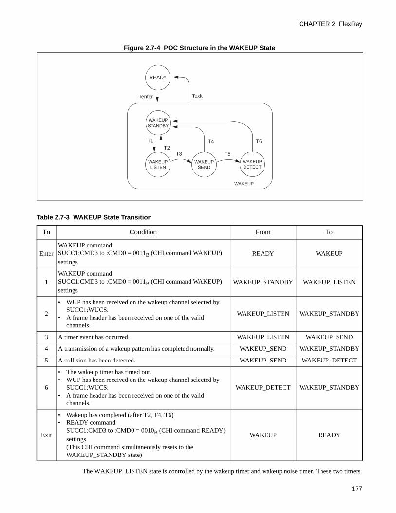
CHAPTER 2 FlexRay
Figure 2.7-4 POC Structure in the WAKEUP State
The WAKEUP_LISTEN state is controlled by the wakeup timer and wakeup noise timer. These two timers
Table 2.7-3 WAKEUP State Transition
Tn Condition From To
EnterWAKEUP command SUCC1:CMD3 to :CMD0 = 0011B (CHI command WAKEUP) settings
READY WAKEUP
1WAKEUP command SUCC1:CMD3 to :CMD0 = 0011B (CHI command WAKEUP) settings
WAKEUP_STANDBY WAKEUP_LISTEN
2
• WUP has been received on the wakeup channel selected by SUCC1:WUCS.
• A frame header has been received on one of the valid channels.
WAKEUP_LISTEN WAKEUP_STANDBY
3 A timer event has occurred. WAKEUP_LISTEN WAKEUP_SEND
4 A transmission of a wakeup pattern has completed normally. WAKEUP_SEND WAKEUP_STANDBY
5 A collision has been detected. WAKEUP_SEND WAKEUP_DETECT
6
• The wakeup timer has timed out. • WUP has been received on the wakeup channel selected by
SUCC1:WUCS. • A frame header has been received on one of the valid
channels.
WAKEUP_DETECT WAKEUP_STANDBY
Exit
• Wakeup has completed (after T2, T4, T6)• READY command
SUCC1:CMD3 to :CMD0 = 0010B (CHI command READY) settings(This CHI command simultaneously resets to the WAKEUP_STANDBY state)
WAKEUP READY
READY
WAKEUPSTANDBY
WAKEUPLISTEN
WAKEUPSEND
WAKEUPDETECT
WAKEUP
T1T2
T3
T4
T5
T6
Tenter Texit
177

CHAPTER 2 FlexRay
are controlled by parameters; Listen Timeout SUCC2:LT20 to LT0 and Listen Timeout Noise
SUCC2:LTN3 to LTN0. Listen Timeout is effective in quick cluster wakeups in a noiseless environment,
whereas Listen Timeout Noise is effective in wakeups in environments with noise interference.
Wakeup patterns are transmitted on configured channels to check their collisions in the WAKEUP_SEND
state. After a transition from the WAKEUP state to READY state, set CMD3 to CMD0 = 0100B (CHI
command RUN) to switch to the STARTUP state.
The cause of a wakeup collision detected in the WAKEUP_SEND state can be identified in the
WAKEUP_DETECT state. The identification stops when it has exceeded Listen Timeout configured by
SUCC2:LT20 to LT0. A direct transition to the READY state occurs either on detection of a wakeup
pattern from other nodes, or reception of a frame header. If neither detection nor reception is performed, a
transition from the WAKEUP_DETECT state occurs after the Listen Timeout has elapsed. In this case, the
cause of the wakeup collisions is unknown.
It is recommended that the startup of a node that will cause a wakeup be delayed for the minimum duration
required for another cold start node to wake up and initialize.
The FlexRay Protocol Specifications V2.1 recommends to wake up two channels using two separate
FlexRay controllers.
■ Host Operations The host must adjust to the waking up of two channels and determine whether or not to wake up specific
channels. The transmission of wakeup patterns is commenced by the host. The receiving bus driver detects
the wakeup pattern and notifies it to the local host.
The host controls the following wakeup procedure (the wakeup procedure for one channel).
• Configures the FlexRay controller in the CONFIG state. Selects the wakeup channel configured by the SUCC1:WUCS bit.
• Checks the bus driver whether it has received WUP or not.
• Activates the bus driver on the selected wakeup channel.
• Writes SUCC1:CMD3 to CMD0 = 0010B in order to transit to the READY state.
• Writes SUCC1:CMD3 to CMD0 = 0011B to start waking up the configured channel.
- The FlexRay controller transits to the WAKEUP state.
- After completing a wakeup, the FlexRay controller transits to the READY state and displays the
wakeup status (CCSV:POCS5 to POCS0).
• Waits for a previously determined duration till other nodes can be woken up and configured.
• The following procedure applies for the cold start node.
- Waits till other channels become WUP in a two channel cluster configuration.
- Write SUCC1:CMD3 to CMD0 = 1001B (CHI command ALLOW_COLDSTART) to reset the cold
start inhibit flag CCSV:CSI.
• Writes SUCC1:CMD3 to CMD0 = 0100B (CHI command RUN) to transit to the STARTUP state.
178

CHAPTER 2 FlexRay
The following wakeup procedure is caused by the bus driver.
• The bus driver identifies a wakeup.
• The bus driver notifies the wakeup event to the host.
• The host configures the FlexRay controller.
• The host may carry out the following if necessary.
- Issues a wakeup command for the second channel.
- Waits for a previously determined duration till other nodes wake up and configure themselves.
• Writes SUCC1:CMD3 to CMD0 = 0100B (CHI command RUN) to transit to the STARTUP state.
■ Wakeup Pattern (WUP)The wakeup pattern (WUP) consists of at least two wakeup symbols (WUS). The wakeup symbol and
wakeup pattern are configured by the PRTC1 register and PRTC2 register.
• The single channel wakeup and wakeup symbol cannot be transmitted on both channels at the same time.
• The wakeup symbol is quick in recovering from signal collisions (two overlapping wakeup symbols are always identifiable) in an environment where there are at least two nodes which transmit wakeup patterns.
• Standardize the wakeup symbol on all nodes in a cluster.
• The "L" time of the wakeup symbol is configured by PRTC2:TXL5 to TXL0.
• The wakeup symbol idle time which is used to listen to activities on the bus is configured by PRTC2:TXI7 to TXI0.
• The wakeup pattern consists of at least two transmission wakeup symbols necessary for the wakeup.
• The number of repetitions (repetitions between 2 and 63) can be configured by PRTC1:RWP5 to RWP0.
• The length of the wakeup symbol reception window is configured by PRTC1:RXW8 to RXW0.
• The "L" time of the wakeup reception is configured by PRTC2:RXL5 to RXL0.
• The wakeup reception idle phase time is configured by PRTC2:RXI5 to RXI0.
Figure 2.7-5 Wakeup Pattern Timing
■ STARTUP StateA node that has been cold started should check while it is in the STARTUP state that both of the initially
connected channels have been woken up.
The time required for all nodes and all clusters to wake up and complete configuration cannot be
estimated.It is recommended that a startup of the node which causes a wakeup be delayed for the minimum
duration required by another cold start node to wakeup, initialize and startup since at least two nodes are
Tx-wakeup Symbol
TXL-15 to 60 bit times TXI = 45 to 180 bit times
Rx-wakeup Pattern(no collision)
Rx-wakeup Pattern(collision, worst case)
179

CHAPTER 2 FlexRay
required for the communications startup.
The time delay caused by all nodes and all clusters to completely wakeup and finish configuration is
approximately several 100 ms (however, this depends on the hardware used).
The startup is carried out on all channels simultaneously. Nodes transmit the startup frames only during the
startup.
The procedure for the error resistant distributed startup is prepared for the initialization synchronization on
all nodes. Generally, nodes transit to the NORMAL_ACTIVE state through the following procedure (see
Figure 2.7-6).
• The cold start procedure to start the scheduled synchronization (leading cold start node).
• The cold start procedure to participate in other cold start nodes (following cold start nodes).
• The integration procedure to join the existing communications schedule (all other nodes).
The attempt at a cold start starts with a transmission of collision avoidance symbols (CAS). Only the cold
start node which transmitted CAS transmits frames during the first four cycles after CAS. Afterwards, other
cold start nodes participate and then all other nodes participate in the cluster.
The cold start node transmits synchronization frames to the key slot by setting "1" to SUCC1:TXST and
SUCC1:TXSY. The message buffer 0 contains the key slot ID which defines the slot number where the
startup frames are transmitted from. The startup frame indicator is set to "1" in the frame header of the
startup frame.
The transmission request flag TXRQ1:TXR0 in the message buffer 0 is reset to "0" after the transmission
of the startup frame. In order to transmit data frames from the message buffer 0, set "1" to TXRQ1:TXR0
via the IBCR register after the transition to the NORMAL_ACTIVE state. Otherwise, a null frame is
transmitted into the slot corresponding to the frame ID stored in the message buffer 0.
Be sure to configure at least three nodes as the cold start node in a cluster consisting of three or more
nodes. Configure both nodes as the cold start node in a cluster consisting of two nodes. At least two
faultless cold start nodes are required to startup a cluster.
The startup frames should be sync frames. Therefore, all cold start nodes are also synchronized nodes. The
number of the cold start attempts is configured by SUCC1:CSA4 to CSA0.
In order for a non-cold start node to join a cluster, at least two startup frames from other nodes are required.
Those non-cold start nodes never complete startup until at least two cold start nodes complete startup.
If a non-cold start node and a cold start node both obtain TDMA (time division multiple access) schedule
information and receive a sync frame, they will soon start a passive join following the integration
procedure. While joining, the nodes adjust their own clock to the global clock (rate and offset) and their
own cycle time to the network global cycle. Afterwards, these configurations are checked on every
available node. Nodes are able to actively join communications only when they have passed these checks.
180

CHAPTER 2 FlexRay
Figure 2.7-6 State Diagram for the Time Triggered Startup
■ Cold Start Inhibit ModeNodes cannot initialize cluster communications in the cold start inhibit mode (CCSV:CSI=1). This means it
is prohibited to commence a startup by the cold start procedure. Such nodes can either join a running
cluster or transmit startup frames after other cold start nodes have started initializing the cluster
communications.
The cold start inhibit bit CCSV:CSI can be configured while POC is in the READY state. Clear this bit by
setting SUCC1:CMD3 to CMD0 = 1001B (CHI command ALLOW_COLDSTART).
READY
ABORTSTARTUP
INTERGRATIONLISTEN
STARTUPPREPARE
INITIALIZESCHEDULE
INTEGRATIONCONSISTENCY
CHECK
NORMALACTIVE
COLDSTARTJOIN
COLDSTARTGAP
COLDSTARTCONSISTENCY
CHECK
INTERGRATIONCOLDSTART
CHECK
COLDSTARTCOLLISION
RESOLUTION
COLDSTARTLISTEN
First coldstart node
Subsequent coldstart nodeNon-coldstart node
ABORT
STARTUP
ABORT
STARTUP
ABORT
STARTUP
ABORT
STARTUP
ABORT
STARTUP
ABORT
STARTUP
STARTUP
181

CHAPTER 2 FlexRay
■ Startup Timeout
The FlexRay controller provides two different µT timers which support two timeout values (startup timeout
and startup noise timeout). These two timers start at the transition to the COLDSTART_LISTEN state.
When one of these two timers ends, the node terminates the other node detection phase (a transition from
the COLDSTART_LISTEN state to another state) in order to start communications.
Note:
The startup timer and startup noise timer are the same as the wakeup timer and wakeup noise timer respectively and SUCC2:LT20 to LT0 and SUCC2:LTN3 to LTN0 are used.
● Startup Timeout
The startup timeout limits the listen time used by nodes in order to determine whether communications are
already established between other nodes, or at least one cold start node is requesting to join other nodes.
The startup timer is configured by SUCC2:LT20 to LT0 (pdListenTimeout).
The startup timer is pdListenTimeout = SUCC2:LT20 to LT0.
The startup timer is restarted by the following.
• A transition to the COLDSTART_LISTEN state
• When both channels reach the idle state in the COLDSTART_LISTEN state
The startup timer is stopped by the following.
• When communications are detected on one configured channel while in the COLDSTART_LISTEN state
• A transition from the COLDSTART_LISTEN state to another state
Once the startup timer passes the restricted time, neither a timer overflow nor periodical restarts occur. The
timer status is retained for future processes.
● Startup Noise Timeout
The startup timer and startup noise timer start when a transition from the STARTUP_PREPARE state to
the COLDSTART_LISTEN state occurs. The startup noise timeout is used to improve the reliability of the
startup procedure in a noisy environment. The startup noise timeout is determined by SUCC2:LTN3 to
LTN0.
The startup noise timer is SUCC2:LT20 to LT0 × (SUCC2:LTN3 to LTN0+1).
The startup noise timeout is calculated as follows.
SUCC2:LT20 to LT0 + (SUCC2:LTN3 to LTN0 × SUCC2:LT20 to LT0)
The startup noise timer is restarted in the following conditions.
• A transition to the COLDSTART_LISTEN state
• A reception of a header or CAS symbol which has been decoded normally in the COLDSTART_LISTEN state
182

CHAPTER 2 FlexRay
The startup noise timer stops at a transition from the COLDSTART_LISTEN state to another state.
Once the startup timer passes the restricted time, neither a timer overflow nor periodical restarts occur. The
timer status is retained for future processes. The startup noise timer does not restart when communication is
detected in any channels.
■ Startup process of the leading cold start node (starting a cold start)When a cold start node is in the COLDSTART_LISTEN state, the node monitors the state of the connected
channels.
If communication is not detected, the node transits to the
COLDSTART_COLLISION_RESOLUTION state and starts a cold start. The first transmission of the CAS
symbol is performed in the normal first cycle. This cycle is called cycle 0.
The node transmits its startup frames from cycle 0. Before all cold start nodes become eligible for a cold
start, some nodes may transmit CAS symbols simultaneously to commence a startup following the cold
start procedure. This state is resolved within the first four cycles after the transmission of CAS.
If any nodes which are starting the cold start receive a CAS symbol or a frame header within these four
cycles, they transit again to the COLDSTART_LISTEN state. As a result, only one node within the cluster
continues the cold start procedure. Other cold start nodes start transmitting their own startup frames in
cycle 4.
Nodes which commence the cold start after four cycles in the COLDSTART_COLLISION_RESOLUTION
state transit to the COLDSTART_CONSISTENCY_CHECK state. These nodes gather all startup frames
from cycle 4 and cycle 5, and adjust the clocks. When the clock correction is carried out without an error
and at least one valid startup frame pair is received, they will transit from the
COLDSTART_CONSISTENCY_CHECK state to the NORMAL_ACTIVE state.
The number of cold start attempts is configured by SUCC1:CSA4 to CSA0. The remaining number of cold
start attempts can be read from CCSV:RCA4 to RCA0. The remaining number of cold start attempts is
decremented each time an attempt is made. When the remaining number of attempts is larger than 1, a
transition to the COLDSTART_LISTEN state is possible, whereas the remaining number of attempts is larger
than "0", a transition to the COLDSTART_COLLISION_RESOLUTION state is possible. Joining a cluster
is possible when the remaining number of cold start attempts is "1", but a cold start is prohibited.
■ Startup process of following cold start nodes (reacting to the leading cold start node)When a cold start node transits to the COLDSTART_LISTEN state, it attempts to receive a valid pair of
startup frames in order to obtain the cycle schedule and clock correction from the leading cold state node.
On reception of the first valid startup frame, it immediately transits to the INITIALIZE_SCHEDULE state.
When it receives the second valid startup frame and obtained the cycle schedule, it transits to the
INTEGRATION_COLDSTART_CHECK state.
183

CHAPTER 2 FlexRay
An accurate clock correction and the use of the leading cold start node (following cold start nodes initialize
their schedule according to this node) are guaranteed in the INTEGRATION_COLDSTART_CHECK
state. Following cold start nodes gather all sync frames and carry out the clock correction in the following
cycle pair. When the clock correction does not show an error and the node continues to receive sufficient
frames from the same node, it transits to the COLDSTART_JOIN state.
Following cold start nodes start transmitting their own startup frames in the COLDSTART_JOIN state and
continue to transmit these frames in the next cycle. This enables the leading cold start node and
participating nodes to check whether their cycle schedules are synchronized. If an error is detected in the
clock correction, the participating node stops the cluster integration. A node in this state transits from the
COLDSTART_JOIN state to the NORMAL_ACTIVE state if it receives at least one valid startup frame in
even number cycles and receives at least one valid pair of startup frames in all cycle pairs. Therefore,
following cold start nodes transit from the STARTUP state to the NORMAL_ACTIVE state at least one
cycle later than the leading cold start node.
■ Startup process of non-cold start nodesWhen a non-cold start node is in the INTEGRATION_LISTEN state, the node monitors the state of
connected channels.
On reception of the first valid startup frame, it immediately transits to the INITIALIZE_SCHEDULE state.
When it receives the second valid startup frame and has obtained the cycle schedule, it transits to the
INTEGRATION_CONSISTENCY_CHECK state.
The non-cold start node checks if the clock correction is correctly operating, and if a sufficient number of
cold start nodes (at least two) are transmitting startup frames with synchronized cycle schedules in the
INTEGRATION_CONSISTENCY_CHECK state. If an error is detected while the clock correction is in
operation, the integration is stopped.
Be sure that this non-cold start node receives two valid startup frames, or receives a valid startup frame
from other integrated nodes within the first even number cycle in this state. Otherwise, the node cancels the
integration.
Be sure that this non-cold start node receives two valid pairs of startup frames, or receives a valid pair of
startup frames from other integrated nodes within the first cycle pair in this state. Otherwise, the node
cancels the integration.
The startup is canceled if two or more valid startup frames are not received within the even number cycle
after the first cycle pair, or if two or more valid pairs of startup frames are not received within one cycle
pair.
In order for a node in this state to transit from the STARTUP state to the NORMAL_ACTIVE state, it must
receive two valid pairs of startup frames each in two cycle pairs. As a result, the node transits from the
STARTUP state to the NORMAL_ACTIVE state at least one cycle pair after a node which has started a
cold start, or at the end of an odd number cycle.
184

CHAPTER 2 FlexRay
■ NORMAL_ACTIVE State The startup phase of the entire cluster completes soon after the node which transmits the first CAS symbol
and one additional node transits to the NORMAL_ACTIVE state. The transmission timing for all
transmission messages is determined in the NORMAL_ACTIVE state. This includes all data frames as well
as sync frames. Measurement of the rate and offset starts in all even number cycles (even/odd number cycle
pairs are required).
The FlexRay controller supports normal communication functions in the NORMAL_ACTIVE state.
• Transmission and reception on the FlexRay bus according to the configuration
• Operation of the clock correction
The FlexRay controller transits to the following states from the NORMAL_ACTIVE state.
• SUCC1:CMD3 to CMD0 = 0110B (CHI command HALT) ⇒ Change to HALT state after the current cycle ends
• SUCC1:CMD3 to CMD0 = 0111B (CHI command FREEZE) ⇒ Immediately change to the HALT state
• The error state changes from ACTIVE to COMM_HALT ⇒ Change to HALT state
• The error state changes from ACTIVE to PASSIVE ⇒ Change to NORMAL_PASSIVE state
• SUCC1:CMD3 to CMD0 = 0010B (CHI command READY) ⇒ Change to READY state
■ NORMAL_PASSIVE StateA transition from the NORMAL_ACTIVE state to the NORMAL_PASSIVE state occurs when the error
state changes from ACTIVE to PASSIVE.
Nodes can receive all frames in the NORMAL_PASSIVE state (nodes can be completely synchronized and
can perform the clock correction). However, nodes do not actively participate in communication unlike in
the NORMAL_ACTIVE state. This means that neither symbols nor frames are transmitted.
The following operations take place in the NORMAL_PASSIVE state.
• Reception of frames on the FlexRay bus
• No transmissions of frames and symbols on the FlexRay bus
• Operation of the clock correction
The FlexRay controller transits to the following states from the NORMAL_PASSIVE state.
• SUCC1:CMD3 to CMD0 = 0110B (CHI command HALT) ⇒ Change to HALT state after the current cycle ends
• SUCC1:CMD3 to CMD0 = 0111B (CHI command FREEZE) ⇒ Immediately change to the HALT state
• The error state changes from PASSIVE to COMM_HALT ⇒ Change to HALT state
• The error state changes from PASSIVE to ACTIVE ⇒ Change to NORMAL_ACTIVE state (This change in the error state occurs when CCEV:PTAC4 to PTAC0 and SUCC1:PTA4 to PTA0-1 become equal.)
• SUCC1:CMD3 to CMD0 = 0010B (CHI command READY) ⇒ Change to READY state
185
CHAPTER 2 FlexRay
■ HALT StateAll communications (transmission and reception) are halted in this state.
The FlexRay controller transits to the HALT state in the following cases.
• From the NORMAL_ACTIVE state or the NORMAL_PASSIVE state when SUCC1:CMD3 to CMD0 = 0110B (CHI command HALT) is written
• From any states when SUCC1:CMD3 to CMD0 = 0111B (CHI command FREEZE) is written
• From the NORMAL_ACTIVE state when the clock correction failed counter has reached the Maximum Without Clock Correction Fatal WCF3 to WCF0
• From the NORMAL_PASSIVE state when the clock correction failed counter has reached the Maximum Without Clock Correction Fatal WCF3 to WCF0
The FlexRay controller transits from this state to the DEFAULT_CONFIG state in the following case.
• When SUCC1:CMD3 to CMD0 = 0001B (CHI command CONFIG) is written
When SUCC1:CMD3 to CMD0 = 0110B (CHI command HALT) is written, the controller sets "1" to the
CCSV:HRQ bit and transits to the HALT state after completing the current communication cycle.
When SUCC1:CMD3 to CMD0 = 0111B (CHI command FREEZE) is written, the controller immediately
transits to the HALT state and sets "1" to the CCSV:FSI bit.
The transition to the HALT state status can be read from CCSV:PSL5 to PSL0.
186

CHAPTER 2 FlexRay
2.7.6 Network Management
This section explains the network management.
■ Network ManagementGenerated network management (NM) vectors can be read from the register (NMV1 to NMV3). The
FlexRay controller performs a bit OR operation on all NM vectors in all valid receive NM frames where
the payload preamble indicator (PPI) is set. Only static frames can be configured as NM frames. Also, NM
vectors are updated after completing each cycle.
The length of the NM vector can be configured between 0 and 12 bytes by NEMC:NML3 to NML0. Be
sure to configure the NM vector length the same on all nodes in the cluster.
Set the PPIT bit in the header section of each transmit buffer to WRHS1:PPIT in order to configure the
frame transmit buffer which is set with the PPIT bit. Also, write NM information into the data section of
each transmit buffer.
Note:
When the message buffer is configured for transmission/reception of the network management frames, configure the payload length in the header 2 of the message buffer equal to or larger than the NM vector length configured in NEMC:NML3 to NML0.
187
CHAPTER 2 FlexRay
2.7.7 Filtering and Masking
This section explains the filtering and masking.
■ Filtering and MaskingFiltering is performed by comparing configurations of the current slot, cycle counter value, channel ID
(ch.A, ch.B) and message buffer. An update or transmission of the message buffer occurs when information
match occurs in this comparison.
Filtering is performed on the followings.
• Slot counter
• Cycle counter
• Channel ID
The following filter combinations are available for filtering at transmission and reception.
• Slot counter + channel ID
• Slot counter + channel ID + cycle counter
Be sure to match all configured filters with receive message information in order to store a receive message
in the message buffer.
Note:
The FIFO acceptance filter is configured by the FIFO rejection filter and the FIFO rejection filter mask.
The time slot corresponding to the frame ID is transmitted on the configured channel. Match the configured
cycle filter value when the cycle counter filtering is available.
■ Slot Counter FilteringAll transmit and receive buffers include the frame ID within the header section. The frame ID is compared
with the current slot counter value in order to assign it to the slot corresponding to the transmit or receive
buffer.
The message buffer with the smallest buffer number is used when two or more buffers are configured with
the same frame ID, and there are matching cycle counter filter values for the same slot on these buffers.
188

CHAPTER 2 FlexRay
■ Cycle Counter Filtering
The concept of cycle counter filtering is based on the cycle set. A match to the filter is detected when an
element of the cycle set matches. The cycle set is defined by the cycle code field in the header section 1 in
each message buffer.
Disable the cycle counter filtering in the message buffer 0 when the message buffer 0 is configured to store
startup/sync frames or single slot frames by bits of SUCC1:TXST, TXSY and TSM.
Note:
Sharing of a static time slot by cycle counter filtering between different nodes in the FlexRay network is not permitted.
The configuration of the number of cycles of a cycle set is described in Table 2.7-4.
The following Table 2.7-5 indicates some examples of valid cycle sets used for cycle counter filtering.
Table 2.7-4 Cycle Set Definitions
Cycle Code Matching Cycle Counter Values
000000xB all Cycles
000001cB every second Cycle at (Cycle Count) mod2 = c
00001ccB every fourth Cycle at (Cycle Count) mod4 = cc
0001cccB every eighth Cycle at (Cycle Count) mod8 = ccc
001ccccB every sixteenth Cycle at (Cycle Count) mod16 = cccc
01cccccB every thirty-second Cycle at (Cycle Count) mod32 = cccc
1ccccccB every sixty-fourth Cycle at (Cycle Count) mod64 = ccccc
Table 2.7-5 Examples of Valid Cycle Set
Cycle Code Matching Cycle Counter Values
0000011B 1-3-5-7- ... -63
0000100B 0-4-8-12- ... -60
0001110B 6-14-22-30- ... -62
0011000B 8-24-40-56
0100011B 3-35
1001001B 9
189

CHAPTER 2 FlexRay
A receive message is stored only when the cycle counter value during the cycle when the message is
received, and the element of the cycle set of the receive buffer match. Satisfy other filter criteria in the
same way.
Contents of the transmit buffer are transmitted to the configured channel when the element of the cycle
configuration and the current cycle counter value match. Satisfy other filter criteria in the same way.
■ Channel ID Filtering2-bit channel filtering fields (CHA, CHB) are included in the header section of the message buffers in the
message RAM. They act as filters for the receive buffer, and as control fields for the transmit buffer (see
Table 2.7-6).
Contents of the transmit buffer are transmitted to the channel specified by the channel filtering field when
slot counter filtering and cycle counter filtering criteria are satisfied. However, a configuration to transmit
to both channels (CHA and CHB) is only permitted in static segments.
Once slot counter filtering and cycle counter filtering criteria are satisfied, valid receive frames are stored if
they are received by the channel specified by the channel filtering field. However, a configuration to
receive frames by both channels (CHA and CHB) is only permitted in static segments.
Note:
Frames are not transmitted and receive frames are ignored when the message buffer is configured for a dynamic segment and both channel filtering field bits (CHA, CHB) are set to "1" (the same function as for CHA = CHB = 0).
■ FIFO Filtering One reject filter and one reject filter mask are prepared as FIFO filtering. The reject filter consists of the
channel filter (FRF:CH1 and CH0), frame ID filter (FRF:FID10 to FID0), and cycle counter filter (FRF:
CYF6 to CYF0). The FRF register and FRFM register can be configured only in the DEFAULT_CONFIG
state or the CONFIG state. The filter configuration in the header section of the message buffer which is a
member of a FIFO group, is ignored.
The 7-bit cycle counter filter (FRF:CYF6 to CYF0) specifies the cycle set and determines the
Table 2.7-6 Channel Filtering Configuration
CHA CHB Transmit Buffer transmit frame Receive Buffer store valid receive frame
1 1on both channels
(static segment only)
received on ch.A or ch.B(store first semantically valid frame,
static segment only)
1 0 on ch.A received on ch.A
0 1 on ch.B received on ch.B
0 0 on transmission ignore frame
190

CHAPTER 2 FlexRay
communication cycle where the frame ID and channel filter is applied on. No frames are received during
the cycle where the frame ID and channel filter are not applied by the cycle set specified by this register.
Valid receive frames are stored in FIFO when the channel ID, frame ID and cycle counter are not rejected
by filtering configured by the rejection filter and rejection filter mask, and also they do not match the
dedicated receive buffer.
191

CHAPTER 2 FlexRay
2.7.8 Transmission Procedure
This section explains the procedures for each of the transmissions.
■ Static SegmentWhen the messages are suspended in a static segment, the message with the frame ID corresponding to the
next transmission slot is selected to be the next transmission message.
The data section of the transmit buffer assigned to a static segment can be updated by the end of the
previous time slot. This means that the starting of a message transmission from the input buffer is done by
writing into the input buffer command request register at the end of the time slot.
■ Dynamic Segment When the messages are suspended in a dynamic segment, the message with the highest priority (the
smallest frame ID) is selected to be the next transmission message. Also, different slot counter columns
may occur on ch.A and ch.B in a dynamic segment (when transmitting simultaneously with different frame
IDs from two channels).
The data section of the transmit buffer assigned to a dynamic segment can be updated by the end of the
previous slot. A message transmission from the input buffer is done by writing into the input buffer
command request register at the end of the time slot.
The transmission complete minislot value (MHDC:SLT12 to SLT0) defines the maximum minislot value
which can be transmitted before prohibiting frame transmissions in the dynamic segment in the current
cycle.
■ Transmit BufferA message buffer can be used as a transmit buffer by setting "1" to the CFG bit in the header section of
each message buffer.
The following methods can be used to assign a transmit buffer to a FlexRay controller channel.
• Static segment: ch.A or ch.B, ch.A and ch.B.
• Dynamic segment: ch.A or ch.B.
The message buffer 0 is set by SUCC1:TXST, TXSY and TSM and can be used as a dedicated buffer for
storing startup frames and sync frames or as a dedicated buffer for specified single slot frames. In this case,
the message buffer 0 can be reconfigured only in the DEFAULT_CONFIG state or the CONFIG state. A
transmission of startup frames/sync frames from other message buffers is not possible.
All message buffers configured for static segments or dynamic segments transmission except buffer 0 can
be reconfigured on the fly by the settings of MRC:SEC1 and SEC0. However, the data partition in the
message RAM is referenced by the data pointer in the header partition. Therefore, care needs to be taken to
192

CHAPTER 2 FlexRay
avoid an incorrect message buffer structure if the payload length and data pointer in the header section of a
message buffer are reconfigured.
Care needs to be taken if a message buffer is reconfigured on the fly (when the header section is updated),
as the message buffer might not be transmitted by each communication cycle.
Be sure to provide the header CRC to all transmit buffers since the FlexRay controller is not equipped with
a function to calculate the header CRC. When network management is required, the host should set "1" to
the PPIT bit in the header section of each message buffer and write network management information into
the data section of these message buffers.
A 2-byte unit payload length is stored into the payload length field. When the payload length of the
configured static transmit buffer is shorter than the configuration by MHDC:SFDL6 to SFDL0, padding
bytes are inserted to guarantee the payload length of the static frame. The padding byte is indicated as "0".
The transmission mode can be configured on each transmit buffer by the transmission mode flag ((TXM).
The transmit message is transmitted in single shot mode when this bit is set to "1". The transmit message is
transmitted in continuous mode when this bit is set to "0".
The TXR127 to TXR0 flags in each message buffer are cleared to "0" after completing the transmission in
single shot mode. After that, overwriting the transmit buffer by the next transmission message becomes
possible.
The TXR127 to TXR0 flags in each message buffer are not cleared to "0" after completing the transmission
in continuous mode. In this case, frames are transmitted each time the filter criteria match. The TXR127 to
TXR0 flags can be cleared to "0" by writing each message buffer number into the IBCR register while the
IBCM:STXRH bit is set to "0".
The transmit buffer with the lowest buffer number is transmitted in each slot when two or more transmit
buffers satisfy the filter criteria.
■ Frame Transmission The following procedure is required to prepare the message buffer for transmissions.
1. Configure the transmit buffer in the message RAM using WRHS1, WRHS2 and WRHS3.
2. Write data into the data section of the transmit buffer using WRDSn.
3. Write the target buffer number into the IBCR register to set the input buffer into the message RAM andtransfer the message data.
4. When the IBCM register is configured for message transmissions, the transmission request flag (TXR)on each message buffer is set to "1" as soon as the transfer from the input buffer is complete and themessage buffer waits for the transmission.
5. Whether the message buffer has completed the transmission or not can be verified by checking the TXRbit (TXR= 0) in the TRXQ1/TRXQ2/TRXQ3/TRXQ4 registers (only in single shot mode).
The TSR127 to TXR0 flags in the TXRQ1/TXRQ2/TXRQ3/TXRQ4 registers are cleared to "0" after
completing the transmission (in single shot mode). Also, SIR:TXI is set to "1" if the MBI bit of the header
section in the message buffer is set to "1". An interrupt occurs if an interrupt is valid.
193

CHAPTER 2 FlexRay
■ Null Frame Transmission The FlexRay controller transmits a null frame with the null frame indicator set to "0" and payload data
cleared to "0", if the transmission request flag is not set to "1" before the transmission time and no other
transmission buffers satisfy the filter criteria in a static segment.
A null frame is transmitted in the following cases.
• When the transmission request flag is not set (TXR = 0) on the message buffer which matches the filter criteria and has the smallest buffer number.
• When all transmit buffers include a cycle counter filter which does not match the current cycle. In this case, the message buffer status (MBS) is updated on the transmit buffer which matches the current slot counter value and has the smallest buffer number.
Null frames are not transmitted in a dynamic segment.
194

CHAPTER 2 FlexRay
2.7.9 Reception Procedure
This section explains the procedures for each of the receptions.
■ Receive BufferA message buffer can be used as a receive buffer by setting "0" to the CFG bit in the header section of the
message buffer.
The following methods can be used to assign a receive buffer to a FlexRay controller channel.
• Static segment: ch.A or ch.B ch.A and ch.B
• Dynamic segment: ch.A or ch.B
The FlexRay controller stores all elements (except the frame CRC) of the frame which matches the filter
criteria for receive buffers.
All receive message buffers configured for static segments or dynamic segments can be reconfigured on the
fly by MRC:SEC1 and SEC0. However, receive messages in each communication cycle might be lost if the
header section in the message buffer is reconfigured on the fly.
The receive buffer with the smallest message buffer number is updated by the receive message if two or
more buffers match the filter criteria.
■ Frame Reception The following procedure is required to prepare the message buffer for receptions.
• Configure the receive buffer in the message RAM using WRHS1, WRHS2 and WRHS3.
• Transfer the configuration from the input buffer to the message RAM by writing the target message buffer number into the IBCR register.
When these steps are carried out, the message buffer starts to function as an active receive buffer and the
acceptance filtering process is performed each time a message is received. The receive buffer which
matches the filter criteria first is updated by the receive message.
Each ND flag in the NDAT1/NDAT2/NDAT3/NDAT4 registers is set to "1" when a valid payload segment
is stored into the data section in the message buffer. Also, the SIR:RXI flag is set to "1" if the MBI bit of
the header section in the message buffer is set to "1". An interrupt occurs if an interrupt is valid.
If the ND bit is already set to "1" when the message buffer is updated, MBS:MLST in the receive message
buffer is set and unprocessed message data is lost.
If there is no frame in a slot, or if a slot receives a null frame or a corrupted frame, no update is performed
195
CHAPTER 2 FlexRay
on the data section in the message buffer which is configured for this slot. In this case, only each message
buffer status flag is updated.
Each MBS flag in the MBSC1/MBSC2/MBSC3/MBSC4 registers is set to "1" when the status flag in the
header section in the message buffer is updated. Also, the SIR:MBSI flag is set to "1" if the MBI bit of the
header section in the message buffer is set to "1". An interrupt occurs if an interrupt is valid.
If the payload length (PLR6 to PLR0) of a receive frame is longer than the value configured in PLC6 to
PLC0 in the header section in each message buffer, the data field stored in the message buffer is shortened
to that length.
Follow the description in "■ Data Transmission from the Message RAM to the Output Buffer" to read the
receive buffer from message RAM through the output buffer.
Note:
ND and MBS flags are cleared to "0" when the payload data and the header of the receive message are transferred to the output buffer respectively.
■ Null Frame Reception The payload segment of a received null frame is not reflected in the receive buffer. If a null frame is
received, the header section of the receive buffer is updated by the received null frame. The null frame
indicator (NFI) in the header section in the received message buffer is cleared to "0".
Each MBS flag in the MBSC1/MBSC2/MBSC3/MBSC4 registers is set to "1" when the status flag in the
header section in the message buffer is updated. Also, the SIR:MBSI flag is set to "1" if the MBI bit of the
header section in the message buffer is set to "1". An interrupt occurs if an interrupt is valid.
196

CHAPTER 2 FlexRay
2.7.10 FIFO Function
This section explains the functions of the FIFO.
■ DetailsOne group of message buffers can be configured as the FIFO buffer. Message buffers belonging to a FIFO
message group are adjacent in the register map. Starting from the message buffer referenced as MRC:FFB7
to FFB0 and ending with the message buffer referenced as MRC:LCB7 to LCB0 is available. A maximum
of 128 message buffers can be assigned to FIFO.
All valid receive messages which do not match the filter criteria of dedicated receive buffers and match the
configured FIFO filter criteria are stored in FIFO. In this case, the frame ID, payload length, receive cycle
count and status bit in the specified FIFO message buffer are overwritten by the receive frame. Also, the
SIR:RFNE bit indicates that FIFO is not empty, and the SIR:RFF bit is set to "1" when the receive FIFO is
becoming full, and the EIR:RFO bit indicates a detection of a FIFO overrun. An interrupt occurs if an
interrupt is valid.
FIFO has two index registers tied to the FIFO, the PUT Index (PIDX) register and the GET Index (GIDX)
register. The PIDX register indicates the position to store the next message in FIFO. When a new message
is received, the message is written into the message buffer specified by the PIDX register. Then the value
of the PIDX register is incremented to point to be stored the message buffer for the next message. When the
value in the PIDX register exceeds the largest message buffer number in the FIFO, it returns to the smallest
message buffer number in the FIFO. The GIDX register is used to specify the next message buffer to be
read in FIFO. The value of the GIDX register is incremented after transferring the contents of the message
buffer belonging to the FIFO message group to the output buffer. Access to the PIDX register and the
GIDX register is not available.
FIFO is full when the value of the PIDX register reaches the value of the GIDX register. When a new
message is written before reading the oldest message in FIFO, both values in the PIDX register and the
GIDX register are incremented and the newest message overwrites the oldest message. This sets "1" to the
EIR:RFO flag.
197

CHAPTER 2 FlexRay
Figure 2.7-7 FIFO Status: Empty, not Empty and Overrun
When the value of the PIDX register and the value of the GIDX register are different, the FIFO not empty
status is detected and the SIR:RFNE flag is set to "1". This indicates that at least one receive message is
present in FIFO. Figure 2.7-7 illustrates the FIFO empty, FIFO not empty and FIFO overrun statuses when
a FIFO contains three message buffers.
The FIFO rejection filter (FRF) defines the filter pattern to reject messages. The filter consists of the
channel filter, frame ID and cycle counter filter. All messages received in a static segment are rejected by
that FIFO filter when the FRF:RSS bit is set to "1". Received null frames are not stored in FIFO when the
FRF:RNF bit is set to "1".
Do not perform rejection filtering using the FIFO Rejection Filter Mask (FRFM) while frame ID filtering is
being performed using the FIFO Rejection Filter register.
■ FIFO Configuration Configure the payload length PLC6 to PLC0 to the same value on all message buffers belonging to FIFO.
Also, configure the data pointer to the top 32-bit word of the data section in each message buffer in the
message RAM.
All information required for the acceptance filter is configured by the FIFO rejection filter and FIFO
rejection filter mask. There is no need to configure the filter criteria on the header section in each message
buffer belonging to FIFO.
Note:
When the payload length of the receive frame exceeds the setting value PLC6 to PLC0 in the header section in each message buffer, the data field stored in the FIFO message buffer is shortened to the length specified in PLC6 to PLC0.
FIFO emptyPIDX
(store next)
FIFO not emptyPIDX
(store next)
FIFO overrunPIDX
(store next)
GIDX(read oldest)
GIDX(read oldest)
GIDX(read oldest)
BuffersMessages
BuffersMessages
BuffersMessages- - - A - - A B C
D
1 2 31 2 31 2 3
• PIDX incremented last• Next received message will be stored into buffer 1• If buffer 1 has not been read, message A is lost.
198

CHAPTER 2 FlexRay
■ Access to FIFOWhen reading from FIFO, transfer the data from the message RAM to the output buffer by writing the first
message buffer number of FIFO (referenced by MRC:FFB7 to FFB0) into the OBCR register. The message
buffer specified by the GIDX register is transferred to the output buffer. After this transfer, the value of the
GIDX register is incremented.
199

CHAPTER 2 FlexRay
2.7.11 Message Handling
This section explains the message handling.
■ Message Handling The message handler controls data transfer between the input/output buffer and the message RAM, and
between the message RAM and two transient buffer RAMs. Every access to the internal RAM is performed
by 32+1 bits unit. The additional bit is used for the parity check.
Access to the message buffer stored in the message RAM is performed under control of the message
handler state machine. This prevents access collisions between hosts to two FlexRay channel protocol
controllers and the message RAM.
Be sure to keep the frame ID of the message buffer assigned to a static segment in the range from 1 to
GTUC7:NSS9 to NSS0. Be sure to keep the frame ID of the message buffer assigned to a dynamic segment
in the range from GTUC7:NSS9 to NSS0 +1 to 2047.
The receive message is stored into receive FIFO (if it is configured so) when it does not match the filter
criteria of the dedicated receive buffer (static segment or dynamic segment) and it matches the filter criteria
of the FIFO rejection filter.
■ Message Buffer ReconfigurationThe static message buffer and dynamic message buffer may be reconfigured while the FlexRay controller is
still operating if the application requires more than 128 message buffers. This can be performed by
updating the header section in each message buffer via the input buffer register (WRHS1 to WRHS3).
Be sure to enable the reconfiguration using the control bits MRC:SEC1 and SEC0 in the message RAM
setting register.
The message is lost if the message buffer has not been updated by a receive frame, or a transmission message
has not been transmitted from the message buffer before the reconfiguration starts.
The timing when transmission or reception is enabled by a reconfiguration of the frame ID for the
reconfigured message buffer depends on the state of the current slot counter when the update of the header
section is complete.
Although the message RAM scan is not complete, it ends at the start of NIT. The message RAM scan for 2
to 15 slots starts from the beginning of slot 1 of the actual cycle. The message RAM scan on slot 1 is
performed before the cycle by checking parallel with each scan on the message RAM even when there is a
message buffer configured for slot 1 of the next cycle.
200
CHAPTER 2 FlexRay
The first dynamic message buffer number is configured by MRC:FDB7 to FDB0. If a message RAM scan
starts while CC is in the dynamic segment, the scan starts from the message buffer number set in
MRC:FDB7 to FDB0.
Follow the following procedure to reconfigure a message buffer in order to use it in slot 1 of the next cycle.
• If the message buffer to be reconfigured for slot 1 is a static buffer, reconfigure the message buffer before it is evaluated by the final message RAM scan in the static segment of the actual cycle.
• If the message buffer to be reconfigured for slot 1 is a static + dynamic buffer, reconfigure the message buffer before it is evaluated by the final message RAM scan in the actual cycle.
• The message RAM scan finishes when the NIT starts. If the message RAM scan was not able to find the reconfigured message buffer, the message buffer is not executed during the next cycle.
Note:
Take care when reconfiguring a message buffer since it may result in a message loss.
■ Host Access to the Message RAMMessage transfers between the input buffer and the message RAM and between the message RAM and the
output buffer start by writing the message buffer number into the IBCR register or the OBCR register
respectively.
The IBCM register and the OBCM register can be used separately to read/write the header section and data
section of the selected message buffer.
When the IBCM:STXRH bit is set to "1", the transmission request flag (TXR) of the message buffer is
automatically set to "1" after the IBCM:STXRS is set to "1" and the selected message buffer is updated.
When the IBCM:STXRH bit is set to "0 ", the IBCM:STXRS bit is cleared to "0" and the transmission
request flag (TXR) of the selected message buffer is cleared to "0". This clearing operation can be used to
stop a transmission on the message buffer which is operating in continuous mode.
The input buffer (IBF) and output buffer (OBF) consist of a double buffer. Among this double buffer
structure, the IBF host/OBF host can be accessed from the host and another IBF shadow/OBF shadow is
accessed by the message handler for data transfer between IBF/OBF and the message RAM.
201

CHAPTER 2 FlexRay
Figure 2.7-8 Host Access to the Message RAM
Host
Dat
a31
to
Dat
a0
Dat
a31
to
Dat
a0
Dat
a31
to
Dat
a0
Dat
a31
to
Dat
a0
Add
ress
Add
ress
Con
trol
Add
ress
Input buffer
[Shadow]
Address decoder and
control
Output buffer
[Shadow]
Message handler
Header Partition
Data Partition
Message RAM
202

CHAPTER 2 FlexRay
■ Data Transmission from the Input Buffer to the Message RAM
To configure or update the message buffers in the message RAM, write the data to WRDSn and write the
header to WRHS1 to WRHS3. A specific operation is selected by setting IBCM.
The IBF host and IBF shadow are swapped by writing the target message buffer number of the message
RAM to IBCR:IBRH6 to IBRH0 (see Figure 2.7-9).
Figure 2.7-9 Double Buffer Structure of the Input Buffer
Also, bits in the IBCM register and the IBCR register are swapped in order to retain the association with
each section in IBF (see Figure 2.7-10).
Figure 2.7-10 Bit Swapping in the IBCM Register and IBCR Register
IBCR:IBSYS is set to "1" by this write operation. The message handler starts transmitting the contents of
the IBF shadow into the message buffer in the message RAM selected by IBCR:IBRS6 to IBRS0.
The next message can be written into the IBF host while the data is transferred from the IBF shadow to the
target message buffer in the message RAM. After completing the transfer between the IBF shadow and the
message RAM and the IBCR:IBSYS bit is cleared to "0", the next transfer to the message RAM is started
by writing the next target message buffer number into IBCR:IBRH6 to IBRH0.
E-Ray
HostIBF host
IBFShad-
ow
IBF = Input buffer
MessageRAM
IBCM IBCR
swapswap18
2
17
1
16
0
31
15
22
6
21
5
20
4
19
3
18
2
17
1
16
0
203
CHAPTER 2 FlexRay
If IBCR:IBRH6 to IBRH0 is written while IBCR:IBSYS=1, IBCR:IBSYH is set to "1". When a data
transfer from the IBF shadow to the message RAM is complete, IBCR:IBSYH is cleared to "0" and "1" is
retained in IBCR:IBSYS, then the next transfer to the message RAM starts. Also, the message buffer
number and the command mask flag stored in IBCR:IBRH6 to IBRH0 and IBCR:IBRS6 to IBRS0 are
swapped simultaneously.
An example of the input buffer configuration procedure:
Configure/update the first message buffer via IBF.
- Write the data section to WRDSn.
- Write the header section to WRHS1 to WRHS3.
- Writing the command mask: write to IBCM:LHSH, LDSH and STXRH.
- Data transfer request to the target message buffer: write to IBCR:IBRH6 to IBRH0.
Configure/update the second message buffer via IBF.
- Write the data section to WRDSn.
- Write the header section to WRHS1 to WRHS3.
- Writing the command mask: write to IBCM:LHSH, LDSH and STXRH.
- Data transfer request to the target message buffer: write to IBCR:IBRH6 to IBRH0 after
IBCR:IBSYH is cleared to "0".
Configure/update the third message buffer via IBF. ...(Repeat the same procedure for the second message buffer)
Note:
An access to the input buffer while IBCR:IBSYH is "1" sets the error flag (EIR:IIBA) to "1". In this case, access is disabled.
Table 2.7-7 Input Buffer Command Mask Bit Assignment
Pos. Access Bit Function
18 R STXRS Set Transmission Request Shadow ongoing or finished
17 R LDSS Load Data Section Shadow ongoing or finished
16 R LHSS Load Header Section Shadow ongoing or finished
2 R/W STXRH Set Transmission Request Host
1 R/W LDSH Load Data Section Host
0 R/W LHSH Load Header Section Host
204

CHAPTER 2 FlexRay
■ Data Transmission from the Message RAM to the Output BufferDo not write into the OBCR register when reading the message buffer from the message RAM since it
causes a data transfer as configured in OBCM. After the transfer is complete, the data transferred from
RDDSn, RDHS1 to RDHS3 and MBS can be read.
Configure the buffer number of the transfer source message buffer in the message RAM by OBCR:OBRS6
to OBRS0.
Figure 2.7-11 Double Buffer Structure of the Output Buffer
As well as each bit in OBCM:RHSS, RDSS, RHSH and RDSH, and each bit in OBCR:OBRS6 to OBRS0
and OBCR:OBRH6 to OBRH0, the OBF host and OBF shadow are swapped according to the configuration
of the OBCR:VIEW bit and OBCR:REQ bit.
Each bit in OBCM:RHSS, RDSS, and OBCR:OBRS6 to OBRS0 are copied into the internal register by
setting the OBCR:REQ bit to "1" (see Figure 2.7-12).
Table 2.7-8 Input Buffer Request Mask Bit Assignment
Pos. Access Bit Function
31 R IBSYSIBF Busy Shadow,signals ongoing transfer from IBF Shadow to Message RAM
22 to 16 RIBRS6 to
BRS0IBF Request Shadow,number of message buffer currently updated
15 R IBSYHIBF Busy Host,transfer request pending for message buffer referenced by IBRH[6:0]
6 to 0 R/WIBRH6 to
IBRH0IBF Request Host,number of message buffer to be updated next
1 R/W LDSH Load Data Section Host
0 R/W LHSH Load Header Section Host
E-Ray
HostOBF host
OBFShad-
ow
OBF = Output buffer
MessageRAM
205

CHAPTER 2 FlexRay
After setting OBCR:REQ to "1", OBCR:OBSYS is set to "1" and the transfer from the message RAM of
the message buffer selected by OBCR:OBRS6 to OBRS0 to the OBF shadow starts. The OBCR:OBSYS
bit is cleared to "0" after completing the transfer from the message RAM to the OBF shadow. OBCR:REQ
and OBCR:VIEW can be set to "1" while OBCR:OBSYS is "0".
Figure 2.7-12 Bit Swapping in the OBCM Register and OBCR Register
The OBF host and OBF shadow can be swapped by setting OBCR:VIEW to "1" while the OBCR:OBSYS
bit is "0" (see Figure 2.7-11). Also, bits of OBCR:OBRH6 to OBRH0, OBCM:RHSH and OBCM:RDSH
are swapped with the internal registers. The internal registers store the values that were copied from
OBCR:OBRS6 to OBRS0, OBCM:RHSS and OBCM:RDSS before OBCR:VIEW was set to "1". By
swapping the internal registers, the message buffer number read from OBCR:OBRH6 to OBRH0 and the
mask configuration read from OBCM:RHSH and OBCM:RDSH are guaranteed to match the transfer data
read from the OBF host (see Figure 2.7-12).
The message buffer which is already transferred can be read from the OBF host after these swaps while the
message handler is able to transfer the next message from the message RAM to the OBF shadow.
An example of the output buffer configuration procedure:
- Transfer request of the first message buffer for the OBF shadow.
- Writing the command mask: write to OBCM:RHSS and OBCM:RDSS.
- Transfer request of the first message buffer: write to OBCR:OBRS6 to OBRS0 and OBCR:REQ.
- Wait until OBCR:OBSYS is cleared to "0".
Transfer request of the second message buffer for the OBF shadow and reading the first message buffer from the OBF host.
- Writing the command mask: write to OBCM:RHSS and RDSS.
- Swapping the OBF host and shadow for the first message, and transfer request of the second
message: write to OBCR:VIEW, REQ and OBRS6 to OBRS0.
- Read the first message.
- Wait until OBCR:OBSYS is cleared to "0".
Transfer request of the third message buffer for the OBF shadow and reading the second message buffer from the OBF host.
- Writing the command mask: write to OBCM:RHSS and RDSS.
- Swapping the OBF host and shadow for the second message, and transfer request of the third
OBCM
17
1
16
01 0
view
request
internal storage
view
request
internal storage
6 5 4 3 2 1 017
1
18
2
19
3
20
4
21
5
22
6
16
015 9 8
206
CHAPTER 2 FlexRay
message: write to OBCR:VIEW, REQ and OBRS6 to OBRS0.
- Read the second message.
- Wait until OBCR:OBSYS is cleared to "0".
(Repeat the same procedure)
Reading the n-th message buffer from the OBF host (when no more message buffer transfer is requested)
- Swapping the OBF host and shadow for the n-th message, and write to OBCR:VIEW (not writing to
OBCR:OBRS6 to OBRS0).
- Read the n-th message.
■ The FlexRay Protocol Controller Access to the Message RAMTwo transient buffer RAMs (TBF A and B) are used as data buffers for transfers between two FlexRay
channel protocol controllers and the message RAM.
The two transient buffer RAMs consist of double buffers and they can store two complete FlexRay
messages. While one buffer is accessible by the message handler, another buffer is assigned to the
corresponding channel protocol controller.
For example, the FlexRay channel protocol controller can store the currently receiving message into the transient
buffer Rx while the message handler is writing a transmit message into the transient buffer Tx. The message
handler (if it passes the acceptance filter) transfers the latest receive message stored in the transient buffer
Rx to the message RAM and updates the message buffer while the message stored in the transient buffer Tx
is being transmitted.
Table 2.7-9 Output Buffer Command Mask Bit Assignment
Pos. Access Bit Function
17 R RDSH Data Section available for Host access
16 R RHSH Header Section available for Host access
1 R/W RDSS Read Data Section Shadow
0 R/W RHSS Read Header Section Shadow
Table 2.7-10 Output Buffer Request Mask Bit Assignment
Pos. Access Bit Function
22 to 16 RIBRH6 to
IBRH0OBF Request Host,number of message buffer available for Host access
15 R OBSYHOBF Busy Shadow,signals ongoing transfer from Message RAM to OBF Shadow
9 R/W REQ Request fransfer from Message RAM to OBF Shadow
9 R/W VIEW View OBF Shadow, swap OBF Shadow and OBF Host
6 to 0 R/WOBR6 to
OBR0OBF Request Shadow,number of message buffer for next request
207

CHAPTER 2 FlexRay
The data transfer between the transient buffer RAM and the shift register of the FlexRay channel protocol
controller is performed in 32-bit word units. This enables the use of 32-bit shift register which has an
independent the length of the FlexRay messages.
Figure 2.7-13 Access to the Transient Buffer RAM
Add
ress
Add
ress
Dat
a31
to
Dat
a0
Dat
a31
to
Dat
a0
Dat
a31
to
Dat
a0
Dat
a31
to
Dat
a0
ControlControl
FlexRay PRT A FlexRay PRT B
Shift registerShift register
Transient Buffer Rx
Transient Buffer Tx
Transient Buffer Rx
Transient Buffer Tx
Add
ress
dec
oder
Add
ress
dec
oder
TBF A TBF B
Message handler
eray_rxd1 eray_txd1 eray_rxd2 eray_txd2
208

CHAPTER 2 FlexRay
2.7.12 Message RAM
This section explains the settings and functions of the message RAM.
■ Message RAMDirect access to the message buffer in the message RAM is not available in order to avoid collisions
between the host access to the message RAM and transmission and reception of FlexRay messages. Access
is processed via the input buffer and output buffer. The message RAM can store up to 128 message buffers.
The message RAM consists of 2048 bytes × 33 bits = 67,584 bits and each 32-bit data is protected by a
parity bit. As the structure of the message RAM is illustrated in Figure 2.7-14, each FlexRay frame can
have variable (0 to 254) number of data bytes.
The data partition starts from (MRC:LCB+1) × 4 words in the message RAM (1 word = 32+1 bits).
Figure 2.7-14 Example of the Message Buffer Configuration in the Message RAM
Header partition
The header partition stores the header section of the configured message buffer.
- A maximum of 128 message buffers are supported.
- Each message buffer has a 4-word (1 word = 32+1 bits) header section.
- The header 3 of each message buffer has a 11-bit data pointer for each data section within the data
partition.
Data partition
The data partition is a variable length memory area which stores data sections with different data length.
Message RAM
Data Partition
Header Partition
Header MB0
Header MB1
Header MBn
Data MBn
Data MB1
•••
Data MB0
Not in use
•••
2048words
33 bits
209

CHAPTER 2 FlexRay
The followings describe the maximum number of message buffers for various data lengths.
- Up to 30 message buffers when each data section is 254 bytes.
- Up to 56 message buffers when each data section is 128 bytes.
- Up to 128 message buffers when each data section is 48 bytes.
Note:
Be sure to configure that the required area of the header partition + data partition is 2048 words (1 word = 33 bits) or less.
■ Header PartitionThe message buffer status and message buffer configuration elements are stored in the header partition of
the message RAM as indicated in Figure 2.7-15. The configuration of the header section of the message
buffer is carried out via IBF (WRHS1 to WRHS3) and reading from the header section is carried out via
OBF (RDHS1 to RDHS3 + MBS). Configure the data pointer in the header section in order to define the
starting position of the data section in each message buffer. Also, do not modify the data pointer while
transferring. Perform reconfigurations on message buffers belonging to the FIFO message group in the
DEFAULT_CONFIG state or the CONFIG state.
The header section of each message buffer occupies 4 words (1 word = 32+1 bits) in the header partition in
the message RAM. The header section of the message buffer 0 starts from the top of the message RAM.
Calculate the header CRC for the transmit buffer.
The received payload length (PLR6 to PLR0), receive cycle count (RCC5 to RCC0), receive channel
indicator (RCI), startup frame indicator (SFI), sync frame indicator (SYN), null frame indicator (NFI),
payload preamble indicator (PPI) and reserved bit (RES) are updated by valid receive frames (including valid
null frames).
The 4-word area in the header of configured each message buffer contains the message buffer status
(MBS).
210

CHAPTER 2 FlexRay
Figure 2.7-15 Header Section of the Message Buffer in the Message RAM
Header 1
The following parameters are written via WRHS1 and read via RDHS1.
- Frame ID : Configuration of slot counter filtering
- Cycle code : Configuration of cycle counter filtering
- CHA, CHB : Configuration of channel filtering
- CFG : Configuration of the message buffer - reception/transmission
- PPIT : Transmission of the payload preamble indicator
- TXM : Configuration of transmission mode - single shot/continuous
- MBI : Enable flag for the message buffer transmission and reception interrupt
Header 2
The following parameters are written via WRHS2 and read via RDHS2.
- Header CRC : Transmit buffer - to be calculated from the frame header segment
: Receive buffer - updated by the receive frame
- Configured payload length : Configured data section length (2-byte units)
- Receive payload length : Payload segment length stored in the receive frame (2-byte units)
BitWord
32 31 30 29 28 27 26 25 24 23 22 21 20 19 18 17 16 15 14 13 12 11 10 9 8 7 6 5 4 3 2 1 0
0 P
P
P
P
P
P
1
2
3
…
…
…
…
Frame IDCycle Code
Payload LengthConfigured
ReceiveCycle Count
Data Pointer
Tx Buffer: Header CRC ConfiguredRx Buffer: Header CRC Received
Payload LengthReceived
MBI
TXM
PPIT
CFG
CHB
CHA
RES
PPI
NFI
SYN
SFI
RCI
MLST
ESB
ESA
TCIB
TCIA
SVOB
SVOA
CEOB
CEOA
SEOB
SEOA
VFRB
VFRA
Frame Configuration (PPIT, CFG, FrameID, Payload Length Configured)
Filter Configuration (CHB, CHA, Cycle Code)
Message Buffer Control (MBI, TXM)
Message RAM Configuration (Data Pointer)
Updated from received Frame (Payload Length Received, RES, PPI, NFI, SYN, SFI, RCI, Receive Cycle Count)
Message Buffer Status MBS (MLST, ESB, ESA, TCIB, TCIA, SVOB, SVOA, CEOB, CEOA, SEOB, SEOA, VFRB, VFRA)
Parity Bit
unused
Cycle Count
FTB
FTA
RESS
PPIS
NFIS
SYNS
SFIS
RCIS
211
CHAPTER 2 FlexRay
Header 3
The following parameters are written via WRHS3 and read via RDHS3.
- Data pointer : Pointer to the starting position of the corresponding data section in the
data partition
The following parameters are read via RDHS3.
These are valid only for receive buffers and updated by receive frames.
- Receive cycle count : Cycle count value stored from the receive frame
- RCI : Receive channel indicator
- SFI : Startup frame indicator
- SYN : Sync frame indicator
- NFI : Null frame indicator
- PPI : Payload preamble indicator
- RES : Reserved bit
Header 4
The header 4 is read via MBS. It is updated at the end of the configured slot.
The following parameters are valid on the transmit buffer and receive buffer.
- VFRA : ch.A valid receive frame
- VFRB : ch.B valid receive frame
- SEOA : ch.A syntax error
- SEOB : ch.B syntax error
- CEOA : ch.A contents error
- CEOB : ch.B contents error
- SVOA : ch.A slot boundary error
- SVOB : ch.B slot boundary error
The following parameters are valid on the transmit buffer only.
- TCIA : ch.A transmission collision indicator
- TCIB : ch.B transmission collision indicator
The following parameters are valid on the receive buffer only.
- ESA : ch.A empty slot
- ESB : ch.B empty slot
- MLST : Message lost
- FTA : ch.A frame transmission
- FTB : ch.B frame transmission
- Cycle Count Status : Actual cycle count at the status update
- RCIS : Channel indicator reception
- SFIS : Startup frame indicator status
- SYNS : Sync frame indicator status
- NFIS : Null frame indicator status
- PPIS : Payload preamble indicator status
- RESS : Reserved bit status
212

CHAPTER 2 FlexRay
■ Data PartitionThe data partition of the message RAM stores the data section of the message buffer which is configured
for reception or transmission as defined in the header partition. The number of data bytes for each message
buffer can be configured in the range from 0 to 254 bytes. The bit width of the message RAM is configured
as 32 bits + 1 parity bit in order to optimize the whole data transfer between the host interface and the
message RAM, and the shift register of 2 FlexRay channel protocol controllers and the message RAM.
The data partition starts immediately after the header partition. Be sure to set the data pointer pointing to
the address within the data partition when configuring the message buffer in the message RAM.
Figure 2.7-16 indicates a storing example to the data partition in the message RAM for the data section of
the configured message buffer.
The starting position and ending position of the data section in the message buffer are determined by the
data pointer and payload length configured in the header section in the message buffer. This enables the
flexible use of RAM space in a message buffer with various data lengths.
When the data section size is an odd number of 2-byte units, the remaining 16 bits in the last 32-bit word
are not used (see Figure 2.7-16).
Figure 2.7-16 Example of the Data Section Structure in the Message RAM
■ Parity CheckThe FlexRay controller is equipped with a parity check mechanism to guarantee the integrity of the data
stored in seven RAM blocks. These RAM blocks include the parity generator/checker connected as
indicated in Figure 2.7-17 and the parity generator generates the parity bit as data is written into the RAM
block. The FlexRay controller employs the even number parity (The parity bit is generated as "0" when the
number of "1"s in the 32-bit word is an even number). The parity bit is stored with the each data. Also, the
parity bit is checked when the data is read from the RAM block. The bit width of the FlexRay controller's
internal data bus is 32 bits.
BitWord
32 31 30 29 28 27 26 25 24 23 22 21 20 19 18 17 16 15 14 13 12 11 10 9 8 7 6 5 4 3 2 1 0
P unused
unused
MBn Data3
…
…
MBn Data(m)
…
…
…
MB1 Data3
…
MB1 Data(k)
MB0 Data3
unused
unused
unused
MBn Data2
…
…
MBn Data(m-1)
…
…
…
MB1 Data2
…
MB1 Data(k-1)
MB0 Data2
unused
unused
unused
MBn Data1
…
…
MBn Data(m-2)
…
…
…
MB1 Data1
…
MB1 Data(k-2)
MB0 Data1
MB0 Data5
unused
unused
MBn Data0
…
…
MBn Data(m-3)
…
…
…
MB1 Data0
…
MB1 Data(k-3)
MB0 Data0
MB0 Data4
…
…
…
…
…
…
…
…
…
…
…
…2046
2047
P
P
P
P
P
P
P
P
P
P
P
P
P
213

CHAPTER 2 FlexRay
Each error flag is set to "1" if a parity error is detected. The message handler status register contains the
parity error flag (MHDS:PIBF, POBF, PMR, PTBF1 and PTBF2) and the faulty message buffer indicator
(MHDS:FMBD, MFMB and FMB6 to FMB0). These error flags control the error interrupt flag EIR:PERR.
Figure 2.7-17 indicates the data path between RAM blocks and the parity generator/checker.
Figure 2.7-17 Parity Generation and Check
Note:
The parity generator and parity checker are blocks independent from the RAM block.
The following operations are performed when a parity error is detected.
On all cases:
The corresponding parity error flag in the MHDS register is set.
The parity error flag EIR:PERR is set. An interrupt occurs if an interrupt is valid.
Special cases:
1) A parity error during a data transfer from the input buffer RAM1, 2 to the message RAM.
• The MHDS:PIBF bit is set.
• The MHDS:FMBD bit is set to indicate that MHDS:FMB6 to FMB0 have been updated.
• MHDS:FMB6 to FMB0 indicate the message buffer number with an error.
• The transmission request bit is not set for the transfer buffer with the parity error.
Input buffer RAM 1, 2
Output buffer RAM 1, 2
TransientBufferRAM A
PG PGPC PC PGPC
TransientBufferRAM B
PGPCPGPC
MessageRAM
PRT A
PRT B
PG PCParity generator Parity checker
214
CHAPTER 2 FlexRay
2) A parity error during a data transfer from the input buffer RAM1, 2 to the host.
• The MHDS:PIBF bit is set.
3) A parity error during a header section scan in the message RAM.
• The MHDS:PMR bit is set.
• The MHDS:FMBD bit is set to indicate that MHDS:FMB6 to FMB0 have been read.
• MHDS:FMB6 to FMB0 indicate the message buffer number with an error.
• The message buffer with the parity error is ignored.
4) A parity error during a data transfer from the message RAM to the transient buffer RAM1, 2.
• The MHDS:PMR bit is set.
• The MHDS:FMBD bit is set to indicate that MHDS:FMB6 to FMB0 have been read.
• MHDS:FMB6 to FMB0 indicate the message buffer number with an error.
• The frame transmission from the message buffer with an error is halted.
5) A parity error during a data transfer from the transient buffer RAM1, 2 to the channel protocol controller 1, 2.
• The MHDS:PTBF1 and PTBF2 bits are set.
• The frame transmission from the transient buffer with an error is halted.
6) A parity error during a data transfer from the transient buffer RAM1, 2 to the message RAM.
• The MHDS:PTBF1 and PTBF2 bits are set.
• The MHDS:FMBD bit is set to indicate that MHDS:FMB6 to FMB0 have been updated.
• MHDS:FMB6 to FMB0 indicate the message buffer number with an error.
7) A parity error during a data transfer from the message RAM to the output buffer RAM.
• The MHDS:PMR bit is set.
• The MHDS:FMBD bit is set to indicate that MHDS:FMB6 to FMB0 have been read.
• MHDS:FMB6 to FMB0 indicate the message buffer number with an error.
8) A parity error during a data transfer from the output buffer RAM to the host.
• The MHDS:POBF bit is set.
9) A parity error while reading data from the transient buffer RAM 1, 2.
The network management vector NMV1 to NMV3 are not updated if a parity error has occurred while the message handler was reading a frame with network management information (PPI=1) from the transient buffer RAM1, 2, or if that frame has no message buffer.
215

CHAPTER 2 FlexRay
2.7.13 Interrupt
This section explains the interrupt operations.
■ InterruptAn interrupt pin is provided for generating interrupts in the event that an error occurs, a status change is
detected, a frame is transmitted or received, or a timer event occurs. This enables an immediate measure to
be taken against errors, status changes and timer events. However, the application may not achieve the
required performance if too many interrupts are generated. Therefore, the FlexRay controller supports a
function to configure each interrupt enabled or disabled.
An interrupt occurs in the following cases.
• An error has been detected.
• A status flag has been set.
• The timer has reached the configured value.
• A message transfer from the input buffer to the message buffer, or the message RAM to the output buffer has completed.
• A stop watch event has occurred.
The event display and interrupt generation for status changes or errors operate as two independent tasks.
Each event is displayed regardless whether the interrupt is enabled or not. Current error information and
status information can be obtained by reading the EIR register and SIR register.
216
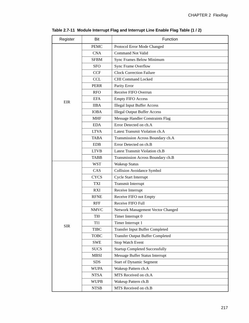
CHAPTER 2 FlexRay
Table 2.7-11 Module Interrupt Flag and Interrupt Line Enable Flag Table (1 / 2)
Register Bit Function
EIR
PEMC Protocol Error Mode Changed
CNA Command Not Valid
SFBM Sync Frames Below Minimum
SFO Sync Frame Overflow
CCF Clock Correction Failure
CCL CHI Command Locked
PERR Parity Error
RFO Receive FIFO Overrun
EFA Empty FIFO Access
IIBA Illegal Input Buffer Access
IOBA Illegal Output Buffer Access
MHF Message Handler Constraints Flag
EDA Error Detected on ch.A
LTVA Latest Transmit Violation ch.A
TABA Transmission Across Boundary ch.A
EDB Error Detected on ch.B
LTVB Latest Transmit Violation ch.B
TABB Transmission Across Boundary ch.B
SIR
WST Wakeup Status
CAS Collision Avoidance Symbol
CYCS Cycle Start Interrupt
TXI Transmit Interrupt
RXI Receive Interrupt
RFNE Receive FIFO not Empty
RFF Receive FIFO Full
NMVC Network Management Vector Changed
TI0 Timer Interrupt 0
TI1 Timer Interrupt 1
TIBC Transfer Input Buffer Completed
TOBC Transfer Output Buffer Completed
SWE Stop Watch Event
SUCS Startup Completed Successfully
MBSI Message Buffer Status Interrupt
SDS Start of Dynamic Segment
WUPA Wakeup Pattern ch.A
NTSA MTS Received on ch.A
WUPB Wakeup Pattern ch.B
NTSB MTS Received on ch.B
217
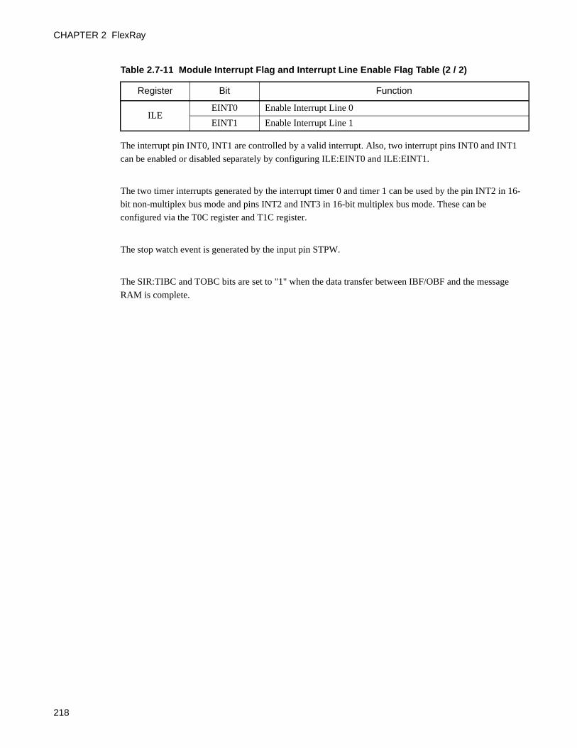
CHAPTER 2 FlexRay
The interrupt pin INT0, INT1 are controlled by a valid interrupt. Also, two interrupt pins INT0 and INT1
can be enabled or disabled separately by configuring ILE:EINT0 and ILE:EINT1.
The two timer interrupts generated by the interrupt timer 0 and timer 1 can be used by the pin INT2 in 16-
bit non-multiplex bus mode and pins INT2 and INT3 in 16-bit multiplex bus mode. These can be
configured via the T0C register and T1C register.
The stop watch event is generated by the input pin STPW.
The SIR:TIBC and TOBC bits are set to "1" when the data transfer between IBF/OBF and the message
RAM is complete.
ILEEINT0 Enable Interrupt Line 0
EINT1 Enable Interrupt Line 1
Table 2.7-11 Module Interrupt Flag and Interrupt Line Enable Flag Table (2 / 2)
Register Bit Function
218

APPENDIX
These appendices explain the I/O registers and configuration parameters.
APPENDIX A I/O Registers
APPENDIX B Configuration Parameters
219

APPENDIX
APPENDIX A I/O Registers
This section shows the I/O registers of the MB88121B.
■ I/O Registers
Table A-1 I/O Registers (1 / 19)
LCK001CH
Lock Register
31 30 29 28 27 26 25 24 23 22 21 20 19 18 17 16
R 0 0 0 0 0 0 0 0 0 0 0 0 0 0 0 0
W
15 14 13 12 11 10 9 8 7 6 5 4 3 2 1 0
R 0 0 0 0 0 0 0 0 0 0 0 0 0 0 0 0
W CLK7 CLK6 CLK5 CLK4 CLK3 CLK2 CLK1 CLK0
EIR 0020H
Error Interrupt Register
31 30 29 28 27 26 25 24 23 22 21 20 19 18 17 16
R 0 0 0 0 0TABB LTVB EDB
0 0 0 0 0 TABA LTVA EDA
W
15 14 13 12 11 10 9 8 7 6 5 4 3 2 1 0
R 0 0 0 0MHF IOBA IIBA EFA RFO PERR CCL CCF SFO SFBM CNA PEM
CW
SIR 0024H
Status Interrupt Register
31 30 29 28 27 26 25 24 23 22 21 20 19 18 17 16
R 0 0 0 0 0 0 MTSB
WUPB
0 0 0 0 0 0 MTSA
WUPAW
15 14 13 12 11 10 9 8 7 6 5 4 3 2 1 0
RSDS MBSI SUCS SWE TOBC TIBC TI1 TI0 NMV
C RFCL RFNE RXI TXI CYCS CAS WSTW
EILS 0028H
Error Interrupt Line Select
31 30 29 28 27 26 25 24 23 22 21 20 19 18 17 16
R 0 0 0 0 0 TABBL
LTVBL EDBL
0 0 0 0 0 TABAL
LTVAL EDAL
W
15 14 13 12 11 10 9 8 7 6 5 4 3 2 1 0
R 0 0 0 0 MHFL
IOBAL IIBAL EFAL RFOL PERR
L CCLL CCFL SFOL SFBML
CNAL
PEMCLW
220

APPENDIX A I/O Registers
SILS 0028H
Status Interrupt Line Select
31 30 29 28 27 26 25 24 23 22 21 20 19 18 17 16
R 0 0 0 0 0 0 MTSBL
WUPBL
0 0 0 0 0 0 MTSAL
WUPALW
15 14 13 12 11 10 9 8 7 6 5 4 3 2 1 0
RSDSL MBSI
LSUCS
LSWE
LTOBC
LTIBC
L TI1L TI0L NMVCL
RFCLL
RFNEL RXIL TXIL CYCS
L CASL WSTLW
EIESEIER0030H0034H
Error Interrupt Enable SetError Interrupt Enable Reset
31 30 29 28 27 26 25 24 23 22 21 20 19 18 17 16
R 0 0 0 0 0 TABBE
LTVBE EDBE
0 0 0 0 0TABAE
LTVAE EDAE
W
15 14 13 12 11 10 9 8 7 6 5 4 3 2 1 0
R 0 0 0 0 MHFE
IOBAE IIBAE EFAE RFOE PERR
E CCLE CCFE SFOE SFBME
CNAE
PEMCE W
SIESSIER 0038H003CH
Status Interrupt Enable SetStatus Interrupt Enable Reset
31 30 29 28 27 26 25 24 23 22 21 20 19 18 17 16
R 0 0 0 0 0 0 MTSBE
WUPBE
0 0 0 0 0 0 MTSAE
WUPAEW
15 14 13 12 11 10 9 8 7 6 5 4 3 2 1 0
RSDSE MBSI
ESUCS
ESWE
ETOBC
E TIBC
E TI1E TI0E NMVCE
RFCLE
RFNEE RXIE TXIE CYCS
E CASE WSTE W
ILE 0040H
Interrupt Line Enable
31 30 29 28 27 26 25 24 23 22 21 20 19 18 17 16
R 0 0 0 0 0 0 0 0 0 0 0 0 0 0 0 0
W
15 14 13 12 11 10 9 8 7 6 5 4 3 2 1 0
R 0 0 0 0 0 0 0 0 0 0 0 0 0 0 EINT1
EINT0W
Table A-1 I/O Registers (2 / 19)
221

APPENDIX
T0C0044H
Timer 0 Configuration
31 30 29 28 27 26 25 24 23 22 21 20 19 18 17 16
R 0 0 T0MO13
T0MO12
T0MO11
T0MO10
T0MO9
T0MO8
T0MO7
T0MO6
T0MO5
T0MO4
T0MO3
T0MO2
T0MO1
T0MO0W
15 14 13 12 11 10 9 8 7 6 5 4 3 2 1 0
R 0 T0CC6
T0CC5
T0CC4
T0CC3
T0CC2
T0CC1
T0CC0
0 0 0 0 0 0T0MS T0RC
W
T1C 0048H
Timer 1 Configuration
31 30 29 28 27 26 25 24 23 22 21 20 19 18 17 16
R 0 0 T1MO13
T1MO12
T1MO11
T1MO10
T1MO9
T1MO8
T1MO7
T1MO6
T1MO5
T1MO4
T1MO3
T1MO2
T1MO1
T1MO0W
15 14 13 12 11 10 9 8 7 6 5 4 3 2 1 0
R 0 0 0 0 0 0 0 0 0 0 0 0 0 0T1MS T1RC
W
STPW1004CH
Stop Watch Register 1
31 30 29 28 27 26 25 24 23 22 21 20 19 18 17 16
R 0 0 SMTV13
SMTV12
SMTV11
SMTV10
SMTV9
SMTV8
SMTV7
SMTV6
SMTV5
SMTV4
SMTV3
SMTV2
SMTV1
SMTV0
W
15 14 13 12 11 10 9 8 7 6 5 4 3 2 1 0
R 0 0 SCCV5
SCCV4
SCCV3
SCCv2
SCCV1
SCCV0 0 EINT
1EINT
0 EETP SSWT EDGE SWMS
ESWTW
STPW20050H
Stop Watch Register 2
31 30 29 28 27 26 25 24 23 22 21 20 19 18 17 16
R 0 0 0 0 0 SSCVB10
SSCVB9
SSCVB8
SSCVB7
SSCVB6
SSCVB5
SSCVB4
SSCVB3
SSCVB2
SSCVB1
SSCVB0
W
15 14 13 12 11 10 9 8 7 6 5 4 3 2 1 0
R 0 0 0 0 0 SSCVA10
SSCVA9
SSCVA8
SSCVA7
SSCVA6
SSCVA5
SSCVA4
SSCVA3
SSCVA2
SSCVA1
SSCVA0
W
Table A-1 I/O Registers (3 / 19)
222

APPENDIX A I/O Registers
SUCC10080H
SUC Configuration Register 1
31 30 29 28 27 26 25 24 23 22 21 20 19 18 17 16
R 0 0 0 0 CCHB*
CCHA*
MTSB*
MTSA*
HCSE* TSM* WUC
S*PTA4
*PTA3
*PTA2
*PTA1
*PTA0
*W
15 14 13 12 11 10 9 8 7 6 5 4 3 2 1 0
R CSA4*
CSA3*
CSA2*
CSA1*
CSA0*
0 TXSY*
TXST*
PBSY 0 0 0 CMD3
CMD2
CMD1
CMD0W
SUCC20084H
SUC Configuration Register 2
31 30 29 28 27 26 25 24 23 22 21 20 19 18 17 16
R 0 0 0 0 LTN3*
LTN2*
LTN1*
LTN0*
0 0 0 LT20*
LT19*
LT18*
LT17*
LT16*W
15 14 13 12 11 10 9 8 7 6 5 4 3 2 1 0
R LT15*
LT14*
LT13*
LT12*
LT11*
LT10* LT9* LT8* LT7* LT6* LT5* LT4* LT3* LT2* LT1* LT0*
W
SUCC30088H
SUC Configuration Register 3
31 30 29 28 27 26 25 24 23 22 21 20 19 18 17 16
R 0 0 0 0 0 0 0 0 0 0 0 0 0 0 0 0
W
15 14 13 12 11 10 9 8 7 6 5 4 3 2 1 0
R 0 0 0 0 0 0 0 0 WCF3*
WCF2*
WCF1*
WCF0*
WCP3*
WCP2*
WCP1*
WCP0*W
NEMC008CH
NEM Configuration Register
31 30 29 28 27 26 25 24 23 22 21 20 19 18 17 16
R 0 0 0 0 0 0 0 0 0 0 0 0 0 0 0 0
W
15 14 13 12 11 10 9 8 7 6 5 4 3 2 1 0
R 0 0 0 0 0 0 0 0 0 0 0 0 NML3*
NML2*
NML1*
NML0*W
PRTC10090H
PRT Configuration Register 1
31 30 29 28 27 26 25 24 23 22 21 20 19 18 17 16
R RWP5*
RWP4*
RWP3*
RWP2*
RWP1*
RWP0*
0 RXW8*
RXW7*
RXW6*
RXW5*
RXW4*
RXW3*
RXW2*
RXW1*
RXW0*W
15 14 13 12 11 10 9 8 7 6 5 4 3 2 1 0
R BRP1*
BRP0* SPP1* SPP0*
0 CASM6* CAS
M5*CASM4*
CASM3*
CASM2*
CASM1*
CASM0*
TSST3*
TSST2*
TSST1*
TSST0*W
Table A-1 I/O Registers (4 / 19)
223
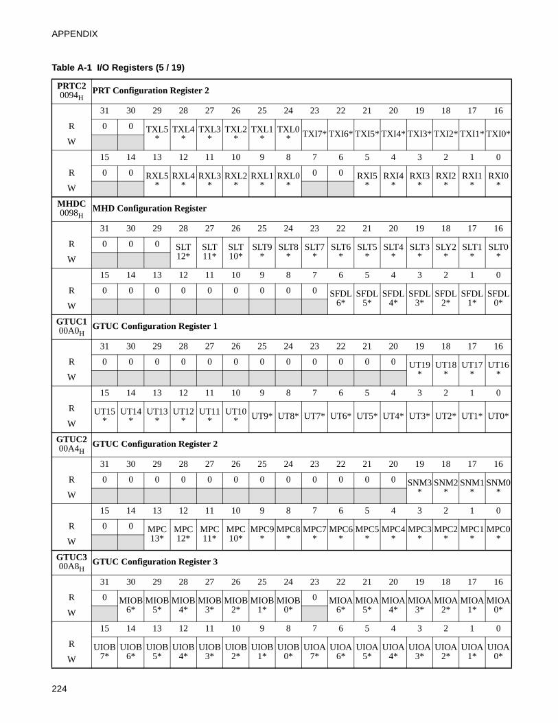
APPENDIX
PRTC20094H
PRT Configuration Register 2
31 30 29 28 27 26 25 24 23 22 21 20 19 18 17 16
R 0 0 TXL5*
TXL4*
TXL3*
TXL2*
TXL1*
TXL0* TXI7* TXI6* TXI5* TXI4* TXI3* TXI2* TXI1* TXI0*
W
15 14 13 12 11 10 9 8 7 6 5 4 3 2 1 0
R 0 0 RXL5*
RXL4*
RXL3*
RXL2*
RXL1*
RXL0*
0 0 RXI5*
RXI4*
RXI3*
RXI2*
RXI1*
RXI0*W
MHDC0098H
MHD Configuration Register
31 30 29 28 27 26 25 24 23 22 21 20 19 18 17 16
R 0 0 0 SLT12*
SLT11*
SLT10*
SLT9*
SLT8*
SLT7*
SLT6*
SLT5*
SLT4*
SLT3*
SLY2*
SLT1*
SLT0*W
15 14 13 12 11 10 9 8 7 6 5 4 3 2 1 0
R 0 0 0 0 0 0 0 0 0 SFDL6*
SFDL5*
SFDL4*
SFDL3*
SFDL2*
SFDL1*
SFDL0*W
GTUC100A0H
GTUC Configuration Register 1
31 30 29 28 27 26 25 24 23 22 21 20 19 18 17 16
R 0 0 0 0 0 0 0 0 0 0 0 0 UT19*
UT18*
UT17*
UT16*W
15 14 13 12 11 10 9 8 7 6 5 4 3 2 1 0
R UT15*
UT14*
UT13*
UT12*
UT11*
UT10* UT9* UT8* UT7* UT6* UT5* UT4* UT3* UT2* UT1* UT0*
W
GTUC200A4H
GTUC Configuration Register 2
31 30 29 28 27 26 25 24 23 22 21 20 19 18 17 16
R 0 0 0 0 0 0 0 0 0 0 0 0 SNM3*
SNM2*
SNM1*
SNM0*W
15 14 13 12 11 10 9 8 7 6 5 4 3 2 1 0
R 0 0 MPC13*
MPC12*
MPC11*
MPC10*
MPC9*
MPC8*
MPC7*
MPC6*
MPC5*
MPC4*
MPC3*
MPC2*
MPC1*
MPC0*W
GTUC300A8H
GTUC Configuration Register 3
31 30 29 28 27 26 25 24 23 22 21 20 19 18 17 16
R 0 MIOB6*
MIOB5*
MIOB4*
MIOB3*
MIOB2*
MIOB1*
MIOB0*
0 MIOA6*
MIOA5*
MIOA4*
MIOA3*
MIOA2*
MIOA1*
MIOA0*W
15 14 13 12 11 10 9 8 7 6 5 4 3 2 1 0
R UIOB7*
UIOB6*
UIOB5*
UIOB4*
UIOB3*
UIOB2*
UIOB1*
UIOB0*
UIOA7*
UIOA6*
UIOA5*
UIOA4*
UIOA3*
UIOA2*
UIOA1*
UIOA0*W
Table A-1 I/O Registers (5 / 19)
224

APPENDIX A I/O Registers
GTUC400ACH
GTUC Configuration Register 4
31 30 29 28 27 26 25 24 23 22 21 20 19 18 17 16
R 0 0 OCS13*
OCS12*
OCS11*
OCS10*
OCS9*
OCS8*
OCS7*
OCS6*
OCS5*
OCS4*
OCS3*
OCS2*
OCS1*
OCS0*W
15 14 13 12 11 10 9 8 7 6 5 4 3 2 1 0
R 0 0 NIT13*
NIT12*
NIT11*
NIT10* NIT9* NIT8* NIT7* NIT6* NIT5* NIT4* NIT3* NIT2* NIT1* NIT0*
W
GTUC500B0H
GTUC Configuration Register 5
31 30 29 28 27 26 25 24 23 22 21 20 19 18 17 16
R DEC7*
DEC6*
DEC5*
DEC4*
DEC3*
DEC2*
DEC1*
DEC0*
0 0 0 CDD4*
CDD3*
CDD2*
CDD1*
CDD0*W
15 14 13 12 11 10 9 8 7 6 5 4 3 2 1 0
R DCB7*
DCB6*
DCB5*
DCB4*
DCB3*
DCB2*
DCB1*
DCB0*
DCA7*
DCA6*
DCA5*
DCA4*
DCA3*
DCA2*
DCA1*
DCA0*W
GTUC600B4H
GTUC Configuration Register 6
31 30 29 28 27 26 25 24 23 22 21 20 19 18 17 16
R 0 0 0 0 0 MOD10*
MOD9*
MOD8*
MOD7*
MOD6*
MOD5*
MOD4*
MOD3*
MOD2*
MOD1*
MOD0*W
15 14 13 12 11 10 9 8 7 6 5 4 3 2 1 0
R 0 0 0 0 0 ASR10*
ASR9*
ASR8*
ASR7*
ASR6*
ASR5*
ASR4*
ASR3*
ASR2*
ASR1*
ASR0*W
GTUC700B8H
GTUC Configuration Register 7
31 30 29 28 27 26 25 24 23 22 21 20 19 18 17 16
R 0 0 0 0 0 0 NSS9*
NSS8*
NSS7*
NSS6*
NSS5*
NSS4*
NSS3*
NSS2*
NSS1*
NSS0*W
15 14 13 12 11 10 9 8 7 6 5 4 3 2 1 0
R 0 0 0 0 0 0 SSL9*
SSL8*
SSL7*
SSL6*
SSL5*
SSL4*
SSL3*
SSL2*
SSL1*
SSL0*W
GTUC800BCH
GTUC Configuration Register 8
31 30 29 28 27 26 25 24 23 22 21 20 19 18 17 16
R 0 0 0 NMS12*
NMS11*
NMS10*
NMS9*
NMS8*
NMS7*
NMS6*
NMS5*
NMS4*
NMS3*
NMS2*
NMS1*
NMS0*W
15 14 13 12 11 10 9 8 7 6 5 4 3 2 1 0
R 0 0 0 0 0 0 0 0 0 0 MSL5*
MSL4*
MSL3*
MSL2*
MSL1*
MSL0*W
Table A-1 I/O Registers (6 / 19)
225

APPENDIX
GTUC900C0H
GTUC Configuration Register 9
31 30 29 28 27 26 25 24 23 22 21 20 19 18 17 16
R 0 0 0 0 0 0 0 0 0 0 0 0 0 0DSI1* DSI0*
W
15 14 13 12 11 10 9 8 7 6 5 4 3 2 1 0
R 0 0 0 MAPO4*
MAPO3*
MAPO2*
MAPO1*
MAPO0*
0 0 APO5*
APO4*
APO3*
APO2*
APO1*
APO0*W
GTUC1000C4H
GTUC Configuration Register 10
31 30 29 28 27 26 25 24 23 22 21 20 19 18 17 16
R 0 0 0 0 0 MRC10*
MRC9*
MRC8*
MRC7*
MRC6*
MRC5*
MRC4*
MRC3*
MRC2*
MRC1*
MRC0*W
15 14 13 12 11 10 9 8 7 6 5 4 3 2 1 0
R 0 0 MOC13*
MOC12*
MOC11*
MOC10*
MOC9*
MOC8*
MOC7*
MOC6*
MOC5*
MOC4*
MOC3*
MOC2*
MOC1*
MOC0*W
GTUC1100C8H
GTUC Configuration Register 11
31 30 29 28 27 26 25 24 23 22 21 20 19 18 17 16
R 0 0 0 0 0 ERC2*
ERC1*
ERC0*
0 0 0 0 0 EOC2*
EOC1*
EOC0*W
15 14 13 12 11 10 9 8 7 6 5 4 3 2 1 0
R 0 0 0 0 0 0 ERCC1*
ERCC0*
0 0 0 0 0 0 EOCC1*
EOCC0*W
CCSV0100H
CC Status Vector
31 30 29 28 27 26 25 24 23 22 21 20 19 18 17 16
R 0 0 PSL5 PSL4 PSL3 PSL2 PSL1 PSL0 RCA4 RCA3 RCA2 RCA1 RCA0 WSV2
WSV1
WSV0
W
15 14 13 12 11 10 9 8 7 6 5 4 3 2 1 0
R 0 CSI CSAI CSNI 0 0 SLM1 SLM0 HRQ FSI POCS5
POCS4
POCS3
POCS2
POCS1
POCS0
W
Table A-1 I/O Registers (7 / 19)
226

APPENDIX A I/O Registers
CCEV0104H
CC Error Vector
31 30 29 28 27 26 25 24 23 22 21 20 19 18 17 16
R 0 0 0 0 0 0 0 0 0 0 0 0 0 0 0 0
W
15 14 13 12 11 10 9 8 7 6 5 4 3 2 1 0
R 0 0 0 PTAC4
PTAC3
PTAC2
PTAC1
PTAC0
ERRM1
ERRM0 0 0 CCFC
3CCFC
2CCFC
1CCFC
0
W
SCV0110H
Slot Counter Value
31 30 29 28 27 26 25 24 23 22 21 20 19 18 17 16
R 0 0 0 0 0 SCCB10
SCCB9
SCCB8
SCCB7
SCCB6
SCCB5
SCCB4
SCCB3
SCCB2
SCCB1
SCCB0
W
15 14 13 12 11 10 9 8 7 6 5 4 3 2 1 0
R 0 0 0 0 0 SCCA10
SCCA9
SCCA8
SCCA7
SCCA6
SCCA5
SCCA4
SCCA3
SCCA2
SCCA1
SCCA0
W
MTCCV0114H
Macrotick and Cycle Counter Value
31 30 29 28 27 26 25 24 23 22 21 20 19 18 17 16
R 0 0 0 0 0 0 0 0 0 0 CCV5 CCV4 CCV3 CCV2 CCV1 CCV0
W
15 14 13 12 11 10 9 8 7 6 5 4 3 2 1 0
R 0 0 MTV13
MTV12
MTV11
MTV10
MTV9
MTV8
MTV7
MTV6
MTV5
MTV4
MTV3
MTV2
MTV1
MTV0
W
RCV0118H
Rate Correction Value
31 30 29 28 27 26 25 24 23 22 21 20 19 18 17 16
R 0 0 0 0 0 0 0 0 0 0 0 0 0 0 0 0
W
15 14 13 12 11 10 9 8 7 6 5 4 3 2 1 0
R 0 0 0 0 RCV11
RCV10 RCV9 RCV8 RCV7 RCV6 RCV5 RCV4 RCV3 RCV2 RCV1 RCV0
W
Table A-1 I/O Registers (8 / 19)
227
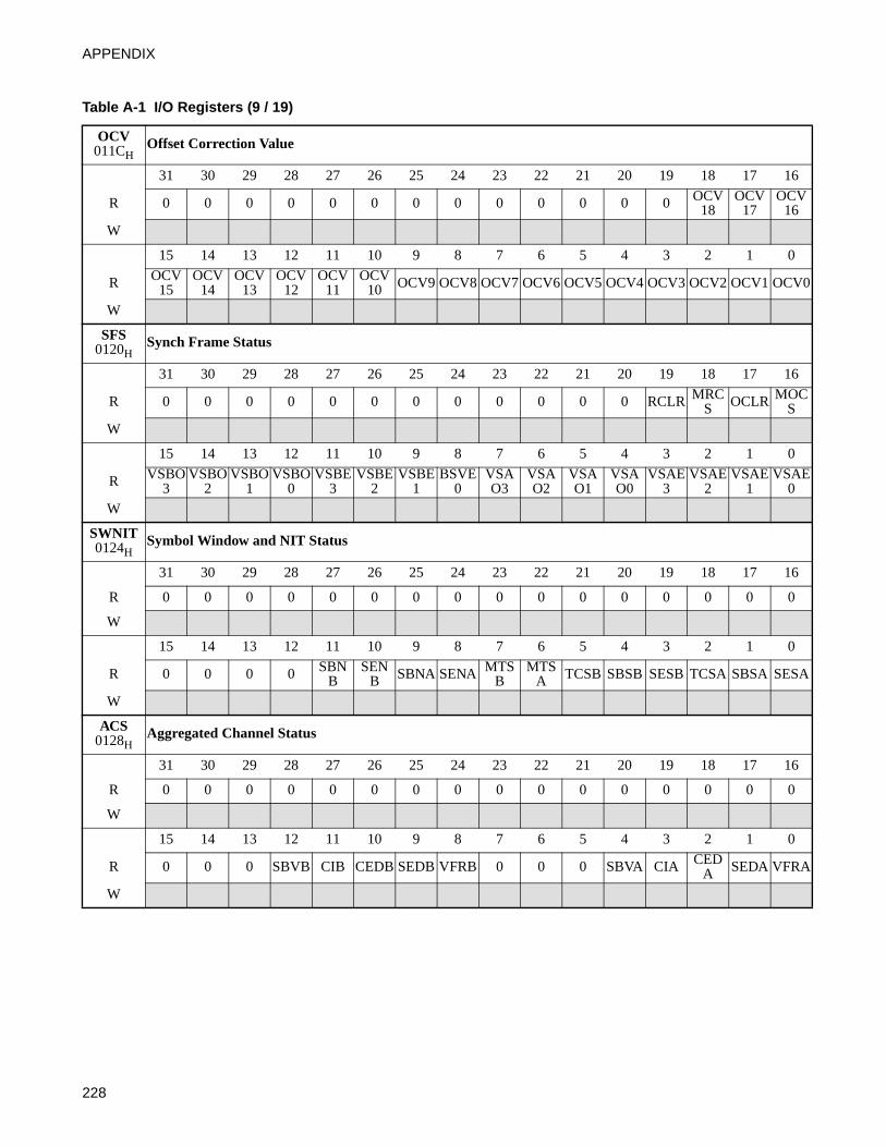
APPENDIX
OCV011CH
Offset Correction Value
31 30 29 28 27 26 25 24 23 22 21 20 19 18 17 16
R 0 0 0 0 0 0 0 0 0 0 0 0 0 OCV18
OCV17
OCV16
W
15 14 13 12 11 10 9 8 7 6 5 4 3 2 1 0
R OCV15
OCV14
OCV13
OCV12
OCV11
OCV10 OCV9 OCV8 OCV7 OCV6 OCV5 OCV4 OCV3 OCV2 OCV1 OCV0
W
SFS0120H
Synch Frame Status
31 30 29 28 27 26 25 24 23 22 21 20 19 18 17 16
R 0 0 0 0 0 0 0 0 0 0 0 0 RCLR MRCS OCLR MOC
S
W
15 14 13 12 11 10 9 8 7 6 5 4 3 2 1 0
R VSBO3
VSBO2
VSBO1
VSBO0
VSBE3
VSBE2
VSBE1
BSVE0
VSAO3
VSAO2
VSAO1
VSAO0
VSAE3
VSAE2
VSAE1
VSAE0
W
SWNIT0124H
Symbol Window and NIT Status
31 30 29 28 27 26 25 24 23 22 21 20 19 18 17 16
R 0 0 0 0 0 0 0 0 0 0 0 0 0 0 0 0
W
15 14 13 12 11 10 9 8 7 6 5 4 3 2 1 0
R 0 0 0 0 SBNB
SENB SBNA SENA MTS
BMTS
A TCSB SBSB SESB TCSA SBSA SESA
W
ACS 0128H
Aggregated Channel Status
31 30 29 28 27 26 25 24 23 22 21 20 19 18 17 16
R 0 0 0 0 0 0 0 0 0 0 0 0 0 0 0 0
W
15 14 13 12 11 10 9 8 7 6 5 4 3 2 1 0
R 0 0 0 SBVB CIB CEDB SEDB VFRB 0 0 0 SBVA CIA CEDA SEDA VFRA
W
Table A-1 I/O Registers (9 / 19)
228

APPENDIX A I/O Registers
ESIDn0130H
to0168H
ESIDn Even Synch ID [1...15]
31 30 29 28 27 26 25 24 23 22 21 20 19 18 17 16
R 0 0 0 0 0 0 0 0 0 0 0 0 0 0 0 0
W
15 14 13 12 11 10 9 8 7 6 5 4 3 2 1 0
R RXEB RXEA 0 0 0 0 EID9 EID8 EID7 EID6 EID5 EID4 EID3 EID2 EID1 EID0
W
OSIDn0170H
to01A8H
OSIDn Odd Synch ID [1...15]
31 30 29 28 27 26 25 24 23 22 21 20 19 18 17 16
R 0 0 0 0 0 0 0 0 0 0 0 0 0 0 0 0
W
15 14 13 12 11 10 9 8 7 6 5 4 3 2 1 0
R RXOB
RXOA 0 0 0 0 OID9 OID8 OID7 OID6 OID5 OID4 OID3 OID2 OID1 OID0
W
NMVn01B0H
to01B8H
Network Management Vector [1...15]
31 30 29 28 27 26 25 24 23 22 21 20 19 18 17 16
R NM31 NM30 NM29 NM28 NM27 NM26 NM25 NM24 NM23 NM22 NM21 NM
20 NM19 NM18 NM17
NM16
W
15 14 13 12 11 10 9 8 7 6 5 4 3 2 1 0
R NM15
NM14
NM13
NM12
NM11
NM10 NM9 NM8 NM7 NM6 NM5 NM4 NM3 NM2 NM1 NM0
W
MRC0300H
MRC Message RAM Configuration
31 30 29 28 27 26 25 24 23 22 21 20 19 18 17 16
R 0 0 0 0 0 SPLM*
SEC1*
SEC0*
LCB7*
LCB6*
LCB5*
LCB4*
LCB3*
LCB2*
LCB1*
LCB0*
W
15 14 13 12 11 10 9 8 7 6 5 4 3 2 1 0
R FFB7*
FFB6*
FFB5*
FFB4*
FFB3*
FFB2*
FFB1*
FFB0*
FDB7*
FDB6*
FDB5*
FDB4*
FDB3*
FDB2*
FDB1*
FDB0*
W
Table A-1 I/O Registers (10 / 19)
229

APPENDIX
FRF0304H
FIFO Rejection Filter
31 30 29 28 27 26 25 24 23 22 21 20 19 18 17 16
R 0 0 0 0 0 0 0RNF* RSS* CYF6
*CYF5
*CYF4
*CYF3
*CYF2
*CYF1
*CYF0
*W
15 14 13 12 11 10 9 8 7 6 5 4 3 2 1 0
R 0 0 0 FID10* FID9* FID8* FID7* FID6* FID5* FID4* FID3* FID2* FID1* FID0* CH1* CH0*
W
FRFM0308H
FIFO Rejection Filter Mask
31 30 29 28 27 26 25 24 23 22 21 20 19 18 17 16
R 0 0 0 0 0 0 0 0 0 0 0 0 0 0 0 0
W
15 14 13 12 11 10 9 8 7 6 5 4 3 2 1 0
R 0 0 0 MFID10*
MFID9*
MFID8*
MFID7*
MFID6*
MFID5*
MFID4*
MFID3*
MFID2*
MFID1*
MFID0*
0 0
W
FCL030CH
FIFO Critical Level
31 30 29 28 27 26 25 24 23 22 21 20 19 18 17 16
R 0 0 0 0 0 0 0 0 0 0 0 0 0 0 0 0
W
15 14 13 12 11 10 9 8 7 6 5 4 3 2 1 0
R 0 0 0 0 0 0 0 0CL7* CL6* CL5* CL4* CL3* CL2* CL1* CL0*
W
MHDS0310H
Message Handler Status
31 30 29 28 27 26 25 24 23 22 21 20 19 18 17 16
R 0 MBU6
MBU5
MBU4
MBU3
MBU2
MBU1
MBU0 0 MBT6 MBT5 MBT4 MBT3 MBT2 MBT1 MBT0
W
15 14 13 12 11 10 9 8 7 6 5 4 3 2 1 0
R 0 FMB6 FMB5 FMB4 FMB3 FMB2 FMB1 FMB0 CRAM MFM
BFMB
DPTBF
2PTBF
1 PMR POBF PIBFW
Table A-1 I/O Registers (11 / 19)
230

APPENDIX A I/O Registers
LDTS0314H
Last Dynamic Transmit Slot
31 30 29 28 27 26 25 24 23 22 21 20 19 18 17 16
R 0 0 0 0 0 LDTB10
LDTB9
LDTB8
LDTB7
LDTB6
LDTB5
LDTB4
LDTB3
LDTB2
LDTB1
LDTB0
W
15 14 13 12 11 10 9 8 7 6 5 4 3 2 1 0
R 0 0 0 0 0 LDTA10
LDTA9
LDTA8
LDTA7
LDTA6
LDTA5
LDTA4
LDTA3
LDTA2
LDTA1
LDTA0
W
FSR0318H
FIFO Status Register
31 30 29 28 27 26 25 24 23 22 21 20 19 18 17 16
R 0 0 0 0 0 0 0 0 0 0 0 0 0 0 0 0
W
15 14 13 12 11 10 9 8 7 6 5 4 3 2 1 0
R RFFL7
RFFL6
RFFL5
RFFL4
RFFL3
RFFL2
RFFL1
RFFL0 0 0 0 0 0 RFO RFCL RFNE
W
MHDF031CH
Message Handler Constraints Flags
31 30 29 28 27 26 25 24 23 22 21 20 19 18 17 16
R 0 0 0 0 0 0 0 0 0 0 0 0 0 0 0 0
W
15 14 13 12 11 10 9 8 7 6 5 4 3 2 1 0
R 0 0 0 0 0 0 0 WAHP
0 0TBFB TBFA FNFB FNFA SNUB SNU
AW
TXRQ10320H
Transmission Request 1
31 30 29 28 27 26 25 24 23 22 21 20 19 18 17 16
R TXR31
TXR30
TXR29
TXR28
TXR27
TXR26
TXR25
TXR24
TXR23
TXR22
TXR21
TXR20
TXR19
TXR18
TXR17
TXR16
W
15 14 13 12 11 10 9 8 7 6 5 4 3 2 1 0
R TXR15
TXR14
TXR13
TXR12
TXR11
TXR10 TXR9 TXR8 TXR7 TXR6 TXR5 TXR4 TXR3 TXR2 TXR1 TXR0
W
Table A-1 I/O Registers (12 / 19)
231

APPENDIX
TXRQ20324H
Transmission Request 2
31 30 29 28 27 26 25 24 23 22 21 20 19 18 17 16
R TXR63
TXR62
TXR61
TXR60
TXR59
TXR58
TXR57
TXR56
TXR55
TXR54
TXR53
TXR52
TXR51
TXR50
TXR49
TXR48
W
15 14 13 12 11 10 9 8 7 6 5 4 3 2 1 0
R TXR47
TXR46
TXR45
TXR44
TXR43
TXR42
TXR41
TXR40
TXR39
TXR38
TXR37
TXR36
TXR35
TXR34
TXR33
TXR32
W
TXRQ30328H
Transmission Request 3
31 30 29 28 27 26 25 24 23 22 21 20 19 18 17 16
R TXR95
TXR94
TXR93
TXR92
TXR91
TXR90
TXR89
TXR88
TXR87
TXR86
TXR85
TXR84
TXR83
TXR82
TXR81
TXR80
W
15 14 13 12 11 10 9 8 7 6 5 4 3 2 1 0
R TXR79
TXR78
TXR77
TXR76
TXR75
TXR74
TXR73
TXR72
TXR71
TXR70
TXR69
TXR68
TXR67
TXR66
TXR65
TXR64
W
TXRQ4032CH
Transmission Request 4
31 30 29 28 27 26 25 24 23 22 21 20 19 18 17 16
R TXR127
TXR126
TXR125
TXR124
TXR123
TXR122
TXR121
TXR120
TXR119
TXR118
TXR117
TXR116
TXR115
TXR114
TXR113
TXR112
W
15 14 13 12 11 10 9 8 7 6 5 4 3 2 1 0
R TXR111
TXR110
TXR109
TXR108
TXR107
TXR106
TXR105
TXR104
TXR103
TXR102
TXR101
TXR100
TXR99
TXR98
TXR97
TXR96
W
NDAT10330H
New Data 1
31 30 29 28 27 26 25 24 23 22 21 20 19 18 17 16
R ND31 ND30 ND29 ND28 ND27 ND26 ND25 ND24 ND23 ND22 ND21 ND20 ND19 ND18 ND17 ND16
W
15 14 13 12 11 10 9 8 7 6 5 4 3 2 1 0
R ND15 ND14 ND13 ND12 ND11 ND10 ND9 ND8 ND7 ND6 ND5 ND4 ND3 ND2 ND1 ND0
W
Table A-1 I/O Registers (13 / 19)
232

APPENDIX A I/O Registers
NDAT20334H
New Data 2
31 30 29 28 27 26 25 24 23 22 21 20 19 18 17 16
R ND63 ND62 ND61 ND60 ND59 ND58 ND57 ND56 ND55 ND54 ND53 ND52 ND51 ND50 ND49 ND48
W
15 14 13 12 11 10 9 8 7 6 5 4 3 2 1 0
R ND47 ND46 ND45 ND44 ND43 ND42 ND41 ND40 ND39 ND38 ND37 ND36 ND35 ND34 ND33 ND32
W
NDAT30338H
New Data 3
31 30 29 28 27 26 25 24 23 22 21 20 19 18 17 16
R ND95 ND94 ND93 ND92 ND91 ND90 ND89 ND88 ND87 ND86 ND85 ND84 ND83 ND82 ND81 ND80
W
15 14 13 12 11 10 9 8 7 6 5 4 3 2 1 0
R ND79 ND78 ND77 ND76 ND75 ND74 ND73 ND72 ND71 ND70 ND69 ND68 ND67 ND66 ND65 ND64
W
NDAT4033CH
New Data 4
31 30 29 28 27 26 25 24 23 22 21 20 19 18 17 16
R ND127
ND126
ND125
ND124
ND123
ND122
ND121
ND120
ND119
ND118
ND117
ND116
ND115
ND114
ND113
ND112
W
15 14 13 12 11 10 9 8 7 6 5 4 3 2 1 0
R ND111
ND110
ND109
ND108
ND107
ND106
ND105
ND104
ND103
ND102
ND101
ND100 ND99 ND98 ND97 ND96
W
MBSC10340H
Message Buffer Status Changed 1
31 30 29 28 27 26 25 24 23 22 21 20 19 18 17 16
R MBC31
MBC30
MBC29
MBC28
MBC27
MBC26
MBC25
MBC24
MBC23
MBC22
MBC21
MBC20
MBC19
MBC18
MBC17
MBC16
W
15 14 13 12 11 10 9 8 7 6 5 4 3 2 1 0
R MBC15
MBC14
MBC13
MBC12
MBC11
MBC10
MBC9
MBC8
MBC7
MBC6
MBC5
MBC4
MBC3
MBC2
MBC1
MBC0
W
Table A-1 I/O Registers (14 / 19)
233
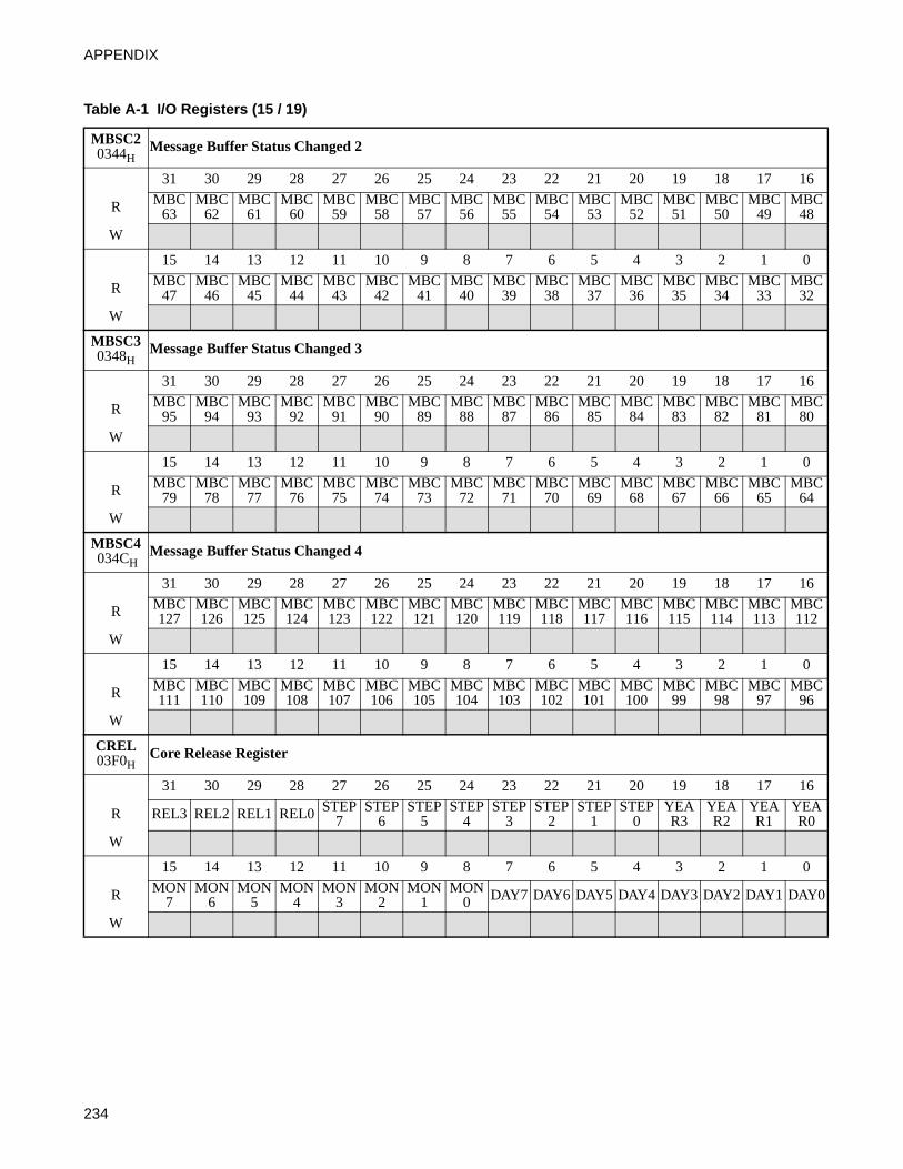
APPENDIX
MBSC20344H
Message Buffer Status Changed 2
31 30 29 28 27 26 25 24 23 22 21 20 19 18 17 16
R MBC63
MBC62
MBC61
MBC60
MBC59
MBC58
MBC57
MBC56
MBC55
MBC54
MBC53
MBC52
MBC51
MBC50
MBC49
MBC48
W
15 14 13 12 11 10 9 8 7 6 5 4 3 2 1 0
R MBC47
MBC46
MBC45
MBC44
MBC43
MBC42
MBC41
MBC40
MBC39
MBC38
MBC37
MBC36
MBC35
MBC34
MBC33
MBC32
W
MBSC3 0348H
Message Buffer Status Changed 3
31 30 29 28 27 26 25 24 23 22 21 20 19 18 17 16
R MBC95
MBC94
MBC93
MBC92
MBC91
MBC90
MBC89
MBC88
MBC87
MBC86
MBC85
MBC84
MBC83
MBC82
MBC81
MBC80
W
15 14 13 12 11 10 9 8 7 6 5 4 3 2 1 0
R MBC79
MBC78
MBC77
MBC76
MBC75
MBC74
MBC73
MBC72
MBC71
MBC70
MBC69
MBC68
MBC67
MBC66
MBC65
MBC64
W
MBSC4 034CH
Message Buffer Status Changed 4
31 30 29 28 27 26 25 24 23 22 21 20 19 18 17 16
R MBC127
MBC126
MBC125
MBC124
MBC123
MBC122
MBC121
MBC120
MBC119
MBC118
MBC117
MBC116
MBC115
MBC114
MBC113
MBC112
W
15 14 13 12 11 10 9 8 7 6 5 4 3 2 1 0
R MBC111
MBC110
MBC109
MBC108
MBC107
MBC106
MBC105
MBC104
MBC103
MBC102
MBC101
MBC100
MBC99
MBC98
MBC97
MBC96
W
CREL03F0H
Core Release Register
31 30 29 28 27 26 25 24 23 22 21 20 19 18 17 16
R REL3 REL2 REL1 REL0 STEP7
STEP6
STEP5
STEP4
STEP3
STEP2
STEP1
STEP0
YEAR3
YEAR2
YEAR1
YEAR0
W
15 14 13 12 11 10 9 8 7 6 5 4 3 2 1 0
R MON7
MON6
MON5
MON4
MON3
MON2
MON1
MON0 DAY7 DAY6 DAY5 DAY4 DAY3 DAY2 DAY1 DAY0
W
Table A-1 I/O Registers (15 / 19)
234

APPENDIX A I/O Registers
ENDN03F4H
Endian Register
31 30 29 28 27 26 25 24 23 22 21 20 19 18 17 16
R ETV31
ETV30
ETV29
ETV28
ETV27
ETV26
ETV25
ETV24
ETV23
ETV22
ETV21
ETV20
ETV19
ETV18
ETV17
ETV16
W
15 14 13 12 11 10 9 8 7 6 5 4 3 2 1 0
R ETV15
ETV14
ETV13
ETV12
ETV11
ETV10 ETV9 ETV8 ETV7 ETV6 ETV5 ETV4 ETV3 ETV2 ETV1 ETV0
W
WRDSn0400H
to04FCH
Write Data Section [1...64]
31 30 29 28 27 26 25 24 23 22 21 20 19 18 17 16
R MD31 MD30 MD29 MD28 MD27 MD26 MD25 MD24 MD23 MD22 MD21 MD20 MD19 MD18 MD17 MD16
W
15 14 13 12 11 10 9 8 7 6 5 4 3 2 1 0
R MD15 MD14 MD13 MD12 MD11 MD10 MD9 MD8 MD7 MD6 MD5 MD4 MD3 MD2 MD1 MD0
W
WRHS10500H
Write Header Section 1
31 30 29 28 27 26 25 24 23 22 21 20 19 18 17 16
R 0 0MBI TXM PPIT CFG CHB CHA
0CYC6 CYC5 CYC4 CYC3 CYC2 CYC1 CYC0
W
15 14 13 12 11 10 9 8 7 6 5 4 3 2 1 0
R 0 0 0 0 0FID10 FID9 FID8 FID7 FID6 FID5 FID4 FID3 FID2 FID1 FID0
W
WRHS20504H
Write Header Section 2
31 30 29 28 27 26 25 24 23 22 21 20 19 18 17 16
R 0 0 0 0 0 0 0 0 0PLC6 PLC5 PLC4 PLC3 PLC2 PLC1 PLC0
W
15 14 13 12 11 10 9 8 7 6 5 4 3 2 1 0
R 0 0 0 0 0 CRC10 CRC9 CRC8 CRC7 CRC6 CRC5 CRC4 CRC3 CRC2 CRC1 CRC0
W
Table A-1 I/O Registers (16 / 19)
235

APPENDIX
WRHS30508H
Write Header Section 3
31 30 29 28 27 26 25 24 23 22 21 20 19 18 17 16
R 0 0 0 0 0 0 0 0 0 0 0 0 0 0 0 0
W
15 14 13 12 11 10 9 8 7 6 5 4 3 2 1 0
R 0 0 0 0 0 DP10* DP9* DP8* DP7* DP6* DP5* DP4* DP3* DP2* DP1* DP0*
W
IBCM 0510H
Input Buffer Command Mask
31 30 29 28 27 26 25 24 23 22 21 20 19 18 17 16
R 0 0 0 0 0 0 0 0 0 0 0 0 0 STXRS LDSS LHSS
W
15 14 13 12 11 10 9 8 7 6 5 4 3 2 1 0
R 0 0 0 0 0 0 0 0 0 0 0 0 0 STXRH LDSH LHSH
W
IBCR0514H
Input Buffer Command Request
31 30 29 28 27 26 25 24 23 22 21 20 19 18 17 16
R IBSYS 0 0 0 0 0 0 0 0 IBRS
6IBRS
5IBRS
4IBRS
3IBRS
2IBRS
1IBRS
0
W
15 14 13 12 11 10 9 8 7 6 5 4 3 2 1 0
R IBSYH 0 0 0 0 0 0 0 0 IBRH
6IBRH
5IBRH
4IBRH
3IBRH
2IBRH
1IBRH
0W
RDDSn0600H
to06FCH
Read Data Section [1...64]
31 30 29 28 27 26 25 24 23 22 21 20 19 18 17 16
R MD31 MD30 MD29 MD28 MD27 MD26 MD25 MD24 MD23 MD22 MD21 MD20 MD19 MD18 MD17 MD16
W
15 14 13 12 11 10 9 8 7 6 5 4 3 2 1 0
R MD15 MD14 MD13 MD12 MD11 MD10 MD9 MD8 MD7 MD6 MD5 MD4 MD3 MD2 MD1 MD0
W
Table A-1 I/O Registers (17 / 19)
236

APPENDIX A I/O Registers
RDHS10700H
Read Header Section 1
31 30 29 28 27 26 25 24 23 22 21 20 19 18 17 16
R 0 0 MBI TXM PPIT CFG CHB CHA 0 CYC6 CYC5 CYC4 CYC3 CYC2 CYC1 CYC0
W
15 14 13 12 11 10 9 8 7 6 5 4 3 2 1 0
R 0 0 0 0 0 FID10 FID9 FID8 FID7 FID6 FID5 FID4 FID3 FID2 FID1 FID0
W
RDHS20704H
Read Header Section 2
31 30 29 28 27 26 25 24 23 22 21 20 19 18 17 16
R 0 PLR6 PLR5 PLR4 PLR3 PLR2 PLR1 PLR0 0 PLC6 PLC5 PLC4 PLC3 PLC2 PLC1 PLC0
W
15 14 13 12 11 10 9 8 7 6 5 4 3 2 1 0
R 0 0 0 0 0 CRC10 CRC9 CRC8 CRC7 CRC6 CRC5 CRC4 CRC3 CRC2 CRC1 CRC0
W
RDHS30708H
Read Header Section 3
31 30 29 28 27 26 25 24 23 22 21 20 19 18 17 16
R 0 0 RES PPI NFI SYN SFI RCI 0 0 RCC5 RCC4 RCC3 RCC2 RCC1 RCC0
W
15 14 13 12 11 10 9 8 7 6 5 4 3 2 1 0
R 0 0 0 0 0 DP10 DP9 DP8 DP7 DP6 DP5 DP4 DP3 DP2 DP1 DP0
W
MBS070CH
Message Buffer Status
31 30 29 28 27 26 25 24 23 22 21 20 19 18 17 16
R 0 0 RESS PPIS NFIS SYNS SFIS RCIS 0 0 CCS5 CCS4 CCS3 CCS2 CCS1 CCS0
W
15 14 13 12 11 10 9 8 7 6 5 4 3 2 1 0
R FTB FTA 0 MLST ESB ESA TCIB TCIA SVOB SVOA CEOB CEO
A SEOB SEOA VFRB VFRA
W
Table A-1 I/O Registers (18 / 19)
237

APPENDIX
* : It can only be written to while in the DEFAULT_CONFIG or CONFIG states.
OBCM0710H
Output Buffer Command Mask
31 30 29 28 27 26 25 24 23 22 21 20 19 18 17 16
R 0 0 0 0 0 0 0 0 0 0 0 0 0 0 RDSH RHSH
W
15 14 13 12 11 10 9 8 7 6 5 4 3 2 1 0
R 0 0 0 0 0 0 0 0 0 0 0 0 0 0RDSS RHSS
W
OBCR0714H
Output Buffer Command Request
31 30 29 28 27 26 25 24 23 22 21 20 19 18 17 16
R 0 0 0 0 0 0 0 0 0 OBRH6
OBRH5
OBRH4
OBRH3
OBRH2
OBRH1
OBRH0
W
15 14 13 12 11 10 9 8 7 6 5 4 3 2 1 0
R OBSYS 0 0 0 0 0
REQ VIEW0 OBRS
6OBRS
5OBRS
4OBRS
3OBRS
2OBRS
1OBRS
0W
Table A-1 I/O Registers (19 / 19)
238
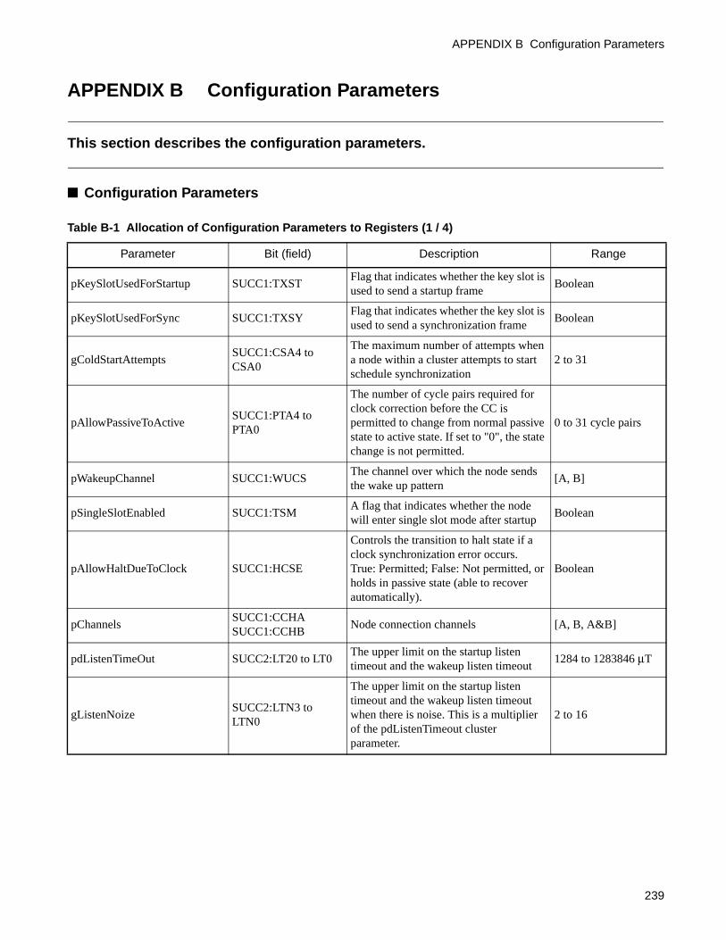
APPENDIX B Configuration Parameters
APPENDIX B Configuration Parameters
This section describes the configuration parameters.
■ Configuration Parameters
Table B-1 Allocation of Configuration Parameters to Registers (1 / 4)
Parameter Bit (field) Description Range
pKeySlotUsedForStartup SUCC1:TXSTFlag that indicates whether the key slot is used to send a startup frame
Boolean
pKeySlotUsedForSync SUCC1:TXSYFlag that indicates whether the key slot is used to send a synchronization frame
Boolean
gColdStartAttemptsSUCC1:CSA4 to CSA0
The maximum number of attempts when a node within a cluster attempts to start schedule synchronization
2 to 31
pAllowPassiveToActiveSUCC1:PTA4 to PTA0
The number of cycle pairs required for clock correction before the CC is permitted to change from normal passive state to active state. If set to "0", the state change is not permitted.
0 to 31 cycle pairs
pWakeupChannel SUCC1:WUCSThe channel over which the node sends the wake up pattern
[A, B]
pSingleSlotEnabled SUCC1:TSMA flag that indicates whether the node will enter single slot mode after startup
Boolean
pAllowHaltDueToClock SUCC1:HCSE
Controls the transition to halt state if a clock synchronization error occurs.True: Permitted; False: Not permitted, or holds in passive state (able to recover automatically).
Boolean
pChannelsSUCC1:CCHASUCC1:CCHB
Node connection channels [A, B, A&B]
pdListenTimeOut SUCC2:LT20 to LT0The upper limit on the startup listen timeout and the wakeup listen timeout
1284 to 1283846 µT
gListenNoizeSUCC2:LTN3 to LTN0
The upper limit on the startup listen timeout and the wakeup listen timeout when there is noise. This is a multiplier of the pdListenTimeout cluster parameter.
2 to 16
239

APPENDIX
gMaxWithoutClockCorrectionPassive
SUCC3:WCP3 to WCP0
The threshold value of the vClockCorrectionFailed counter test. The number of cycle pairs for clock correction when beginning a transition from normal active state to passive state.Note that gMaxWithoutClockCorrectionPassive<=gMaxWithoutClockCorrectionFatal<=15.
1 to 15 cycle pairs
gMaxWithoutClockCorrectionFatal
SUCC3:WCF3 to WCF0
The threshold value of the vClockCorrectionFailed counter test. The number of cycle paris for clock correction when beginnning a transition from normal active state or passive state to halt state.
gMaxWithoutClockCorrectPassive to 15
gNetworkManagementVectorLength
NEMC:NML3 to NML0
The length of the cluster network management vector
0 to 12 bytes
gdTSSTransmitterPRTC1:TSST3 to TSST0
The number of bits in the transmission start sequence
3 to 15 gdBit
gdCASRxLowMaxPRTC1:CASM6 to CASM0
The upper limit on the CAS receive window
67 to 99 gdBit
gdSampleClockPeriod PRTC1:BRP1, BRP0 The period of the sample clock 12.5ns, 25.0ns, 50.0ns
pSamplesPerMicrotick PRTC1:BRP1, BRP0 The number of samples per microtick [1, 2, 4]
gdWakeupSymbolRxWindowPRTC1:RXW8 to RXW0
The number of bits for testing the symbol length of received wakeup symbols. =30µs+α
76 to 301 gdBit
pWakeupPatternPRTC1:RWP5 to RWP0
The number of repetitions of the wakeup symbol generated by the wakeup pattern when the node enters the wakeup send state.
2 to 63
gdWakeupSymbolRxIdle PRTC2:RXI5 to RXI0The number of bits for testing the idle length of received wakeup symbols. =6µs-α
14 to 59 gdBit
gdWakeupSymbolRxLowPRTC2:RXL5 to RXL0
The number of bits for testing the low length of received wakeup symbols. =6µs-α
10 to 55 gdBit
gdWakeupSymbolTxIdle PRTC2:TXI7 to TXI0The number of bits to send in the idle portion of the wakeup symbol. =6µs
45 to 180 gdBit
gdWakeupSymbolTxLowPRTC2:TXL5 to TXL0
The number of bits to send in the "L" portion of the wakeup symbol. =6µs
15 to 60 gdBit
gPayloadLengthStaticMHDC:SFDL6 to SFDL0
The payload length of static frames0 to cPayloadLengthMax two-byte words
pLatestTxMHDC:SLT12 to SLT0
The final minislot number within a dynamic segment at which frame transmission can be started
Minislot 0 to 7981
Table B-1 Allocation of Configuration Parameters to Registers (2 / 4)
Parameter Bit (field) Description Range
240

APPENDIX B Configuration Parameters
pMicroPerCycle GTUC1:UT19 to UT0The number of microticks in the local node communication cycle.
640 to 640000 µT
gMacroPerCycleGTUC2:MPC13 to MPC0
The number of macroticks in the communication cycle
10 to 16000 MT
gSyncNodeMaxGTUC2:SNM3 to SNM0
The number of nodes that can send frames that have the sync frame bit set
2 to cSyncNodeMax
pMicroInitialOffset[A]GTUC3:UIOA7 to UIOA0
The number of microticks in each of the macrotick boundaries defined by the gMacroInitialOffset and the secondary reference point. Configured separately for each channel.
0 to 240 µT
pMicroInitialOffset[B]GTUC3:UIOB7 to UIOB0
do. 0 to 240 µT
pMacroInitialOffset[A]GTUC3:MIOA6 to MIOA0
The number of macroticks between the static slot boundary and the next macrotick boundary.
2 to 72 MT
pMacroInitialOffset[B]GTUC3:MIOB6 to MIOB0
do. 2 to 72 MT
gdNITGTUC4:NIT13 to NIT0
The length of the network idle time 2 to 767 MT
gOffsetCorrectionStartGTUC4:OCS13 to OCS0
The starting point of the internal NIT offset correction phase. This is the number of microticks from the starting point of the cycle.
9 to 15999 MT
pDelayCompensation[A]GTUC5:DCA7 to DCA0
The receive delay compensation value for ch.A. The microticks from 0.0125 µs to 0.05 µs correspond to the propagation delay up to cPropagationDelayMax.
0 to 200 µT
pDelayCompensation[B]GTUC5:DCB7 to DCB0
The receive delay compensation value for ch.B. The microticks from 0.0125 µs to 0.05 µs correspond to the propagation delay up to cPropagationDelayMax.
0 to 200 µT
pClusterDriftDampingGTUC5:CDD4 to CDD0
The local cluster drift damping factor used for rate correction
0 to 20 µT
pDecodingCorrectionGTUC5:DEC7 to DEC0
The number of microticks for calculations between time reference points.
14 to 143 µT
pdAcceptedStartupRangeGTUC6:ASR10 to ASR0
The maximum variation in the real-time clock permitted in the startup frame during integration
0 to 1875 µT
pdMaxDriftGTUC6:MOD10 to MOD0
The maximum drift offset between two nodes that are operating on unsynchronized clocks in a single communication cycle
2 to 1923µT
gdStaticSlot GTUC7:SSL9 to SSL0 Static slot length 4 to 659 MT
Table B-1 Allocation of Configuration Parameters to Registers (3 / 4)
Parameter Bit (field) Description Range
241

APPENDIX
gNumberOfStaticSlotsGTUC7:NSS9 to NSS0
The number of static slots in a static segment
2 to cStaticSlotIDMax
gdMinislotGTUC8:MSL5 to MSL0
Minislot length 2 to 63 MT
gNumberOfMinislotsGTUC8:NMS12 to NMS0
The number of minislots in a dynamic slot
0 to 7986
gdActionPointOffsetGTUC9:APO5 to APO0
The number of action point offsets from the beginning of a static slot or a symbol window
1 to 63 MT
gdMinislotActionPointOffsetGTUC9:MAPO4 to MAPO0
The number of minislot action point offsets from the beginning of a minislot
1 to 31 MT
gdDynamicSlotIdlePhase GTUC9:DSI1, DSI0 The dynamic slot idle phase length 0 to 2 Minislot
pOffsetCorrectionOutGTUC10:MOC13 to MOC0
The upper limit of the permissible offset correction
5 to 15266 µT
pRateCorrectionOutGTUC10:MRC10 to MRC0
The upper limit of the permissible offset correction
2 to 1923µT
pExternOfsetCorrectonGTUC11:EOC2 to EOC0
The number of microticks that the host adds to or subtracts from the NIT for external offset correction
0 to 7 µT
pExternRateCorrectionGTUC11:ERC2 to ERC0
The number of microticks that the host adds to or subtracts from the NIT for external rate correction
0 to 7 µT
Table B-1 Allocation of Configuration Parameters to Registers (4 / 4)
Parameter Bit (field) Description Range
242

INDEX
INDEX
The index follows on the next page.This is listed in alphabetic order.
243

INDEX
Index
Numerics
16-bit Multiplex Parallel Bus16-bit Multiplex Parallel Bus Timing .................132
16-bit Non-multiplex Parallel Bus16-bit Non-multiplex Parallel Bus Timing ..........127
A
ACSAggregated Channel Status (ACS)....................... 87
Aggregated Channel StatusAggregated Channel Status (ACS)....................... 87
AlgorithmData Security Algorithm ................................... 153
B
Baud RateSetting Example of the FlexRay Baud Rate
......................................................... 162Block Diagram
Block Diagram of FlexRay controller .................. 30Block Diagram of the MB88121B ......................... 3
Byte StructureCommand Byte Structure.................................. 144
C
CCCommunication Controller (CC) Control Registers
........................................................... 61Communication Controller (CC) Status Registers
........................................................... 78CC Error Vector Register
CC Error Vector Register (CCEV)....................... 81CC Status Vector Register
CC Status Vector Register (CCSV)...................... 78CCEV
CC Error Vector Register (CCEV)....................... 81CCNT
Clock Control Register (CCNT) .......................... 37CCSV
CC Status Vector Register (CCSV)...................... 78Channel ID Filtering
Channel ID Filtering ........................................ 190Clock
Clock Correction Failed Counter ....................... 170Clock Synchronization ..................................... 168External Clock Synchronization ........................ 169FlexRay Controller Clock ................................. 158RAM Clock Configuration................................ 161Serial Clock Operations .................................... 142Serial Clock Operations Setting......................... 142Switching Procedure to the PLL Clock............... 160Switching Procedure to the Reference Clock
......................................................... 160Switching the System Clock Divider Value ........ 161
244
INDEX
Clock Control RegisterClock Control Register (CCNT) .......................... 37
Cold Start Inhibit ModeCold Start Inhibit Mode .................................... 181
Cold Start NodeStartup process of following cold start nodes
(reacting to the leading cold start node).......................................................... 183
Startup process of the leading cold start node (starting a cold start)............................ 183
Combination of RBC and WBCRBCWBC: Combination of RBC and WBC (78H)
.......................................................... 149Combination of RBC and WBI
RBCWBI: Combination of RBC and WBI (72H).......................................................... 148
Combination of RBI and WBCRBIWBC: Combination of RBI and WBC (5AH)
.......................................................... 148Combination of RBI and WBI
RBIWBI: Combination of RBI and WBI (50H).......................................................... 147
CommandCommand Byte Structure.................................. 144FREEZE Command ......................................... 171HALT Command ............................................. 171WRIBC: Write Input Buffer Command (90H)
.......................................................... 150WROBC: Write Output Buffer Command (9AH)
.......................................................... 151Communication Controller
Communication Controller (CC) Control Registers............................................................ 61
Communication Controller (CC) Status Registers............................................................ 78
Communication CycleCommunication Cycle ...................................... 164
Communication ModeCommunication Mode ...................................... 167
Communications Controller StatesDiagram of the Communications Controller States
.......................................................... 172CONFIG State
CONFIG State ................................................. 174Configuration Parameters
Configuration Parameters ................................. 239Continue
RBC: Read Output Buffer,Continue (60H).......... 147WBC: Write Input Buffer,Continue (18H) .......... 146
Core Release RegisterCore Release Register (CREL) .......................... 108
CorrectionOffset (Phase) Correction.................................. 169Rate (Frequency) Correction ............................. 169
CRELCore Release Register (CREL)...........................108
Customer RegistersCustomer Registers .............................................35
Cycle Counter FilteringCycle Counter Filtering .....................................189
D
Data PartitionData Partition ...................................................213
Data Security AlgorithmData Security Algorithm....................................153
DBGSDebug Support Register (DBGS) .........................40
Debug Support RegisterDebug Support Register (DBGS) .........................40
DEFAULT_CONFIG StateDEFAULT_CONFIG State ...............................174
Divider ValueSwitching the System Clock Divider Value
..........................................................161DMA Operations
DMA Operations ..............................................138DMA Support Register
DMA Support Register (DMAS) ..........................41DMAS
DMA Support Register (DMAS) ..........................41Dynamic Segment
Dynamic Segment ....................................165, 192
E
EIERError Interrupt Enable Set/Reset Registers
(EIES,EIER) .........................................54EIES
Error Interrupt Enable Set/Reset Registers (EIES,EIER) .........................................54
EILSError Interrupt Line Select Register (EILS) ...........52
EIRError Interrupt Register (EIR) ..............................46
Endian RegisterEndian Register (ENDN)...................................109
ENDNEndian Register (ENDN)...................................109
Error HandlingError Handling .................................................170
Error Interrupt Enable Set/Reset Registers Error Interrupt Enable Set/Reset Registers
(EIES,EIER) .........................................54Error Interrupt Line Select Register
Error Interrupt Line Select Register (EILS) ...........52
245

INDEX
Error Interrupt RegisterError Interrupt Register (EIR)..............................46
ESIDEven Numbered Cycle Sync Frame ID Register
(ESID1 to ESID15) ...............................89Even Numbered Cycle Sync Frame ID Register
Even Numbered Cycle Sync Frame ID Register (ESID1 to ESID15) ...............................89
External ClockExternal Clock Synchronization.........................169
F
Failed CounterClock Correction Failed Counter........................170
FCLFIFO Critical Level Register (FCL) .....................96
FIFOAccess to FIFO ................................................199FIFO Configuration ..........................................198
FIFO Critical Level RegisterFIFO Critical Level Register (FCL) .....................96
FIFO FilteringFIFO Filtering..................................................190
FIFO Rejection Filter Mask RegisterFIFO Rejection Filter Mask Register (FRFM)
............................................................95FIFO Rejection Filter Register
FIFO Rejection Filter Register (FRF) ...................94FIFO Status Register
FIFO Status Register (FSR).................................99Filtering
Channel ID Filtering .........................................190Cycle Counter Filtering.....................................189FIFO Filtering..................................................190Filtering and Masking .......................................188Slot Counter Filtering .......................................188
FlexRayBlock Diagram of FlexRay controller ...................30Configuration of FlexRay....................................33FlexRay Channel Protocol Controller (PRT A/B)
............................................................31FlexRay Controller Clock .................................158FlexRay Features................................................29FlexRay Operations ..........................................127FlexRay Protocol Function ................................163Overview of FlexRay..........................................28Setting Example of the FlexRay Baud Rate
..........................................................162The FlexRay Protocol Controller Access to the
Message RAM ....................................207FlexRay Channel Protocol Controller
FlexRay Channel Protocol Controller (PRT A/B)............................................................31
FlexRay ControllerBlock Diagram of FlexRay controller .................. 30FlexRay Controller Clock ................................. 158
FlexRay Protocol ControllerThe FlexRay Protocol Controller Access to the
Message RAM .................................... 207Frame
Frame Reception.............................................. 195Frame Transmission ......................................... 193Null Frame Reception ...................................... 196Null Frame Transmission.................................. 194Sync Frame Transmission ................................. 169
Frame and Symbol ProcessingFrame and Symbol Processing (FSP) ................... 32
FREEZE CommandFREEZE Command ......................................... 171
FrequencyRate (Frequency) Correction ............................. 169
FRFFIFO Rejection Filter Register (FRF)................... 94
FRFMFIFO Rejection Filter Mask Register (FRFM)
........................................................... 95FSP
Frame and Symbol Processing (FSP) ................... 32FSR
FIFO Status Register (FSR) ................................ 99Functional Description
Functional Description of Each Block .................... 4
G
Global TimeGlobal Time .................................................... 168Global Time Unit (GTU) .................................... 31
GTU Configuration RegisterGTU Configuration Register 1 (GTUC1) ............. 70GTU Configuration Register 10 (GTUC10) .......... 76GTU Configuration Register 11 (GTUC11) .......... 77GTU Configuration Register 2 (GTUC2) ............. 71GTU Configuration Register 3 (GTUC3) ............. 71GTU Configuration Register 4 (GTUC4) ............. 72GTU Configuration Register 5 (GTUC5) ............. 73GTU Configuration Register 6 (GTUC6) ............. 74GTU Configuration Register 7 (GTUC7) ............. 74GTU Configuration Register 8 (GTUC8) ............. 75GTU Configuration Register 9 (GTUC9) ............. 75
GTUCGTU Configuration Register 1 (GTUC1) ............. 70GTU Configuration Register 10 (GTUC10) .......... 76GTU Configuration Register 11 (GTUC11) .......... 77GTU Configuration Register 2 (GTUC2) ............. 71GTU Configuration Register 3 (GTUC3) ............. 71GTU Configuration Register 4 (GTUC4) ............. 72GTU Configuration Register 5 (GTUC5) ............. 73
246

INDEX
GTU Configuration Register 6 (GTUC6).............. 74GTU Configuration Register 7 (GTUC7).............. 74GTU Configuration Register 8 (GTUC8).............. 75GTU Configuration Register 9 (GTUC9).............. 75
H
HALT CommandHALT Command ............................................. 171
HALT StateHALT State ..................................................... 186
Handling DevicesNotes on Handling Devices ................................. 19
Header PartitionHeader Partition ............................................... 210
Header SectionWRHS: Write Input Buffer Header Section 1 to 3
(AAH) ................................................ 152Host
Host Access to the Message RAM ..................... 201Host Operations ............................................... 178
I
I/O CircuitI/O Circuit Types ............................................... 18
I/O MapI/O Map ............................................................ 21
I/O RegistersI/O Registers ................................................... 220
IBCMInput Buffer Command Mask Register (IBCM)
.......................................................... 114IBCR
Input Buffer Command Request Register (IBCR).......................................................... 115
Idle TimeNetwork Idle Time (NIT).................................. 165
ILEInterrupt Line Enable Register (ILE).................... 56
InitializeRBI: Read Output Buffer,Initialize (42H) ........... 146WBI: Write Input Buffer,Initialize (12H) ............ 145
Input BufferData Transmission from the Input Buffer to the
Message RAM .................................... 203Input Buffer..................................................... 110Input Buffer Data Transfer ................................ 139WBC: Write Input Buffer,Continue (18H) .......... 146WBI: Write Input Buffer,Initialize (12H) ............ 145WIP: Write Input Buffer Pointer (82H)............... 149WRHS: Write Input Buffer Header Section 1 to 3
(AAH) ................................................ 152WRIBC: Write Input Buffer Command (90H)
.......................................................... 150
Input Buffer Command Mask RegisterInput Buffer Command Mask Register (IBCM)
..........................................................114Input Buffer Command Request Register
Input Buffer Command Request Register (IBCR)..........................................................115
INTInterrupt Control (INT) .......................................32Interrupt Register (INT) ......................................43
InterruptInterrupt...........................................................216Interrupt Control (INT) .......................................32
Interrupt ControlInterrupt Control (INT) .......................................32
Interrupt Line Enable RegisterInterrupt Line Enable Register (ILE) ....................56
Interrupt RegisterInterrupt Register (INT) ......................................43
L
Last Dynamic Transmit Slot RegisterLast Dynamic Transmit Slot Register (LDTS)
............................................................99LCK
Lock Register (LCK) ..........................................45LDTS
Last Dynamic Transmit Slot Register (LDTS)............................................................99
Local TimeLocal Time ......................................................168
Lock RegisterLock Register (LCK) ..........................................45
LSBLSB/MSB Settings ...........................................141
M
Macrotick and Cycle Counter Value RegisterMacrotick and Cycle Counter Value Register
(MTCCV) .............................................82Masking
Filtering and Masking .......................................188MB88121B
Block Diagram of the MB88121B ..........................3MBS
Message Buffer Status Register (MBS)...............120MBSC
Message Buffer Status Changed Register 1/2/3/4 (MBSC1/MBSC2/MBSC3/MBSC4)..........................................................105
MDSMDS1 Pin= "H" ,MDS0 Pin= "H" ......................143MDS1 Pin= "H" ,MDS0 Pin= "L" ......................143MDS1 Pin= "L" ,MDS0 Pin= "H" ......................143
247

INDEX
MDS1 Pin= "L" ,MDS0 Pin= "L" ......................142Message
Data Transmission from the Input Buffer to the Message RAM ....................................203
Data Transmission from the Message RAM to the Output Buffer......................................205
Host Access to the Message RAM .....................201Message Handling ............................................200Message RAM .................................................209The FlexRay Protocol Controller Access to the
Message RAM ....................................207Message Buffer
Message Buffer Reconfiguration........................200Message Buffer Status Changed Register
Message Buffer Status Changed Register 1/2/3/4 (MBSC1/MBSC2/MBSC3/MBSC4)..........................................................105
Message Buffer Status RegisterMessage Buffer Status Register (MBS) ..............120
Message Handler Constraints FlagsMessage Handler Constraints Flags (MHDF)
..........................................................100Message Handler Status Register
Message Handler Status Register (MHDS) ...........97Message RAM Configuration Register
Message RAM Configuration Register (MRC)............................................................92
MHD Configuration RegisterMHD Configuration Register (MHDC) ................70
MHDCMHD Configuration Register (MHDC) ................70
MHDFMessage Handler Constraints Flags (MHDF)
..........................................................100MHDS
Message Handler Status Register (MHDS) ...........97Mode
Cold Start Inhibit Mode ....................................181Communication Mode ......................................167Operation Mode Settings...................................141Restoration Procedure from Stop Mode ..............161Switching Procedure to Stop Mode ....................160
MONITOR_MODEMONITOR_MODE..........................................175
MRCMessage RAM Configuration Register (MRC)
............................................................92MSB
LSB/MSB Settings ...........................................141MTCCV
Macrotick and Cycle Counter Value Register (MTCCV).............................................82
Multiplex Parallel Bus16-bit Multiplex Parallel Bus Timing .................132
MultiplierPLL Multiplier Setting ..................................... 141
N
NDATNew Data Register 1/2/3/4
(NDAT1/NDAT2/NDAT3/NDAT4)......................................................... 103
NEMNetwork Management (NEM) ............................. 32
NEM Configuration RegisterNEM Configuration Register (NEMC)................. 67
NEMCNEM Configuration Register (NEMC)................. 67
Network Idle TimeNetwork Idle Time (NIT).................................. 165
Network ManagementNetwork Management ...................................... 187Network Management (NEM) ............................. 32Network Management Vector
(NMV1 to NMV3: [1 to 3]).................... 90New Data Register
New Data Register 1/2/3/4 (NDAT1/NDAT2/NDAT3/NDAT4)......................................................... 103
NITNetwork Idle Time (NIT).................................. 165Starting NIT and Configuring the Offset Correction
Start................................................... 166NMV
Network Management Vector (NMV1 to NMV3: [1 to 3]).................... 90
NodeStartup process of following cold start nodes
(reacting to the leading cold start node)......................................................... 183
Startup process of the leading cold start node (starting a cold start)............................ 183
NoiseNoise Prevention................................................ 20
Non-cold StartStartup process of non-cold start nodes .............. 184
Non-multiplex Parallel Bus16-bit Non-multiplex Parallel Bus Timing .......... 127
NOPNOP: Read Status (00H) ................................... 152
NORMAL_ACTIVE StateNORMAL_ACTIVE State................................ 185
NORMAL_PASSIVE StateNORMAL_PASSIVE State .............................. 185
Null FrameNull Frame Reception ...................................... 196Null Frame Transmission.................................. 194
248
INDEX
O
OBCMOutput Buffer Command Mask Register (OBCM)
.......................................................... 124OBCR
Output Buffer Command Request Register (OBCR).......................................................... 125
OCVOffset Correction Value Register (OCV) .............. 83
Odd Numbered Cycle Sync Frame ID RegisterOdd Numbered Cycle Sync Frame ID Register
(OSID1 to OSID15) .............................. 90Offset
Offset (Phase) Correction.................................. 169Offset Correction Start
Starting NIT and Configuring the Offset Correction Start................................................... 166
Offset Correction Value RegisterOffset Correction Value Register (OCV) .............. 83
Operation ModeOperation Mode Settings .................................. 141
OSIDOdd Numbered Cycle Sync Frame ID Register
(OSID1 to OSID15) .............................. 90Output Buffer
Data Transmission from the Message RAM to the Output Buffer ..................................... 205
Output Buffer .................................................. 117Output Buffer Data Transfer ............................. 140RBC: Read Output Buffer,Continue (60H)
.......................................................... 147RBI: Read Output Buffer,Initialize (42H) ........... 146WOP: Write Output Buffer Pointer (88H) ........... 150WROBC: Write Output Buffer Command (9AH)
.......................................................... 151Output Buffer Command Mask Register
Output Buffer Command Mask Register (OBCM).......................................................... 124
Output Buffer Command Request RegisterOutput Buffer Command Request Register (OBCR)
.......................................................... 125
P
Package DimensionsPackage Dimensions ............................................ 7
Parallel Bus16-bit Multiplex Parallel Bus Timing ................. 13216-bit Non-multiplex Parallel Bus Timing .......... 127
Parity CheckParity Check .................................................... 213
PartitionData Partition .................................................. 213Header Partition ............................................... 210
PhaseOffset (Phase) Correction ..................................169
Pin AssignmentPin Assignment ....................................................8
Pin FunctionsPin Functions .....................................................11
PLL ClockSwitching Procedure to the PLL Clock ...............160
PLL MultiplierPLL Multiplier Setting ......................................141
PointerWIP: Write Input Buffer Pointer (82H) ...............149WOP: Write Output Buffer Pointer (88H)............150
ProtocolFlexRay Protocol Function ................................163SPI Protocol Definition .....................................144The FlexRay Protocol Controller Access to the
Message RAM.....................................207PRT
FlexRay Channel Protocol Controller (PRT A/B)............................................................31
PRT Configuration RegisterPRT Configuration Register 1 (PRTC1)................68PRT Configuration Register 2 (PRTC2)................69
PRTCPRT Configuration Register 1 (PRTC1)................68PRT Configuration Register 2 (PRTC2)................69
R
RAMData Transmission from the Input Buffer to the
Message RAM.....................................203Data Transmission from the Message RAM to the
Output Buffer ......................................205Host Access to the Message RAM......................201Message RAM .................................................209RAM Clock Configuration ................................161The FlexRay Protocol Controller Access to the
Message RAM.....................................207Transient Buffer RAM (TBF A/B) .......................31
RateRate (Frequency) Correction..............................169
Rate Correction Value RegisterRate Correction Value Register (RCV) .................83
RBCRBC: Read Output Buffer,Continue (60H) ..........147RBCWBC: Combination of RBC and WBC (78H)
..........................................................149RBCWBI: Combination of RBC and WBI (72H)
..........................................................148RBCWBC
RBCWBC: Combination of RBC and WBC (78H)..........................................................149
249

INDEX
RBCWBIRBCWBI: Combination of RBC and WBI (72H)
..........................................................148RBI
RBI: Read Output Buffer,Initialize (42H)............146RBIWBC: Combination of RBI and WBC (5AH)
..........................................................148RBIWBI: Combination of RBI and WBI (50H)
..........................................................147RBIWBC
RBIWBC: Combination of RBI and WBC (5AH)..........................................................148
RBIWBIRBIWBI: Combination of RBI and WBI (50H)
..........................................................147RCV
Rate Correction Value Register (RCV) .................83RDDS
Read Data Section Register (RDDS1 to RDDS64)..........................................................117
RDHSRead Header Section Register 1 (RDHS1) ..........118Read Header Section Register 2 (RDHS2) ..........118Read Header Section Register 3 (RDHS3) ..........119
RDNRDN: Read Word n (A0H) ................................151
RDYRDY Wait Count......................................129, 134
Read Data Section RegisterRead Data Section Register (RDDS1 to RDDS64)
..........................................................117Read Header Section Register
Read Header Section Register 1 (RDHS1) ..........118Read Header Section Register 2 (RDHS2) ..........118Read Header Section Register 3 (RDHS3) ..........119
Read OperationsRegister Read Operations ..........................130, 134
Read Output Buffer,ContinueRBC: Read Output Buffer,Continue (60H) ..........147
Read Output Buffer,InitializeRBI: Read Output Buffer,Initialize (42H)............146
Read WordRDN: Read Word n (A0H) ................................151
READY StateREADY State ..................................................175
Receive BufferReceive Buffer .................................................195
ReceptionFrame Reception ..............................................195Null Frame Reception .......................................196
Reference ClockSwitching Procedure to the Reference Clock
..........................................................160
RegisterCC Error Vector Register (CCEV)....................... 81CC Status Vector Register (CCSV)...................... 78Clock Control Register (CCNT) .......................... 37Communication Controller (CC) Control Registers
........................................................... 61Communication Controller (CC) Status Registers
........................................................... 78Core Release Register (CREL) .......................... 108Debug Support Register (DBGS)......................... 40DMA Support Register (DMAS) ......................... 41Endian Register (ENDN) .................................. 109Error Interrupt Enable Set/Reset Registers
(EIES,EIER)......................................... 54Error Interrupt Line Select Register (EILS) .......... 52Error Interrupt Register (EIR) ............................. 46Even Numbered Cycle Sync Frame ID Register
(ESID1 to ESID15) ............................... 89FIFO Critical Level Register (FCL) ..................... 96FIFO Rejection Filter Mask Register (FRFM)
........................................................... 95FIFO Rejection Filter Register (FRF)................... 94FIFO Status Register (FSR) ................................ 99GTU Configuration Register 1 (GTUC1) ............. 70GTU Configuration Register 10 (GTUC10) .......... 76GTU Configuration Register 11 (GTUC11) .......... 77GTU Configuration Register 2 (GTUC2) ............. 71GTU Configuration Register 3 (GTUC3) ............. 71GTU Configuration Register 4 (GTUC4) ............. 72GTU Configuration Register 5 (GTUC5) ............. 73GTU Configuration Register 6 (GTUC6) ............. 74GTU Configuration Register 7 (GTUC7) ............. 74GTU Configuration Register 8 (GTUC8) ............. 75GTU Configuration Register 9 (GTUC9) ............. 75Input Buffer Command Mask Register (IBCM)
......................................................... 114Input Buffer Command Request Register (IBCR)
......................................................... 115Interrupt Line Enable Register (ILE).................... 56Interrupt Register (INT)...................................... 43Last Dynamic Transmit Slot Register (LDTS)
........................................................... 99Lock Register (LCK).......................................... 45Macrotick and Cycle Counter Value Register
(MTCCV) ............................................ 82Message Buffer Status Changed Register 1/2/3/4
(MBSC1/MBSC2/MBSC3/MBSC4)......................................................... 105
Message Buffer Status Register (MBS) .............. 120Message Handler Status Register (MHDS) ........... 97Message RAM Configuration Register (MRC)
........................................................... 92MHD Configuration Register (MHDC) ................ 70NEM Configuration Register (NEMC)................. 67New Data Register 1/2/3/4
(NDAT1/NDAT2/NDAT3/NDAT4)......................................................... 103
250
INDEX
Odd Numbered Cycle Sync Frame ID Register (OSID1 to OSID15) .............................. 90
Offset Correction Value Register (OCV) .............. 83Output Buffer Command Mask Register (OBCM)
.......................................................... 124Output Buffer Command Request Register (OBCR)
.......................................................... 125PRT Configuration Register 1 (PRTC1) ............... 68PRT Configuration Register 2 (PRTC2) ............... 69Rate Correction Value Register (RCV)................. 83Read Data Section Register (RDDS1 to RDDS64)
.......................................................... 117Read Header Section Register 1 (RDHS1) .......... 118Read Header Section Register 2 (RDHS2) .......... 118Read Header Section Register 3 (RDHS3) .......... 119Register Read Operations.......................... 130, 134Register Write Operations......................... 131, 136Slot Counter Value Register (SCV)...................... 82Status Interrupt Enable Set/Reset Registers
(SIES,SIER) ......................................... 55Status Interrupt Line Select Register (SILS) ......... 53Status Interrupt Register (SIR) ............................ 49Stop Watch Register 1 (STPW1) ......................... 59Stop Watch Register 2 (STPW2) ......................... 60SUC Configuration Register 1 (SUCC1) .............. 61SUC Configuration Register 2 (SUCC2) .............. 66SUC Configuration Register 3 (SUCC3) .............. 66Symbol Window and NIT Status Register (SWNIT)
............................................................ 85Sync Frame Status Register (SFS) ....................... 84Timer 0 Configuration Register (T0C) ................. 56Timer 1 Configuration Register (T1C) ................. 57Transmission Request Register 1/2/3/4
(TXRQ1/TXRQ2/TXRQ3/TXRQ4).......................................................... 102
Version Information Register (VER).................... 35Write Data Section Register (WRDS1 to WRDS64)
.......................................................... 110Write Header Section Register 1 (WRHS1) ........ 111Write Header Section Register 2 (WRHS2) ........ 113Write Header Section Register 3 (WRHS3) ........ 113
Required CycleRequired Cycle Pair Counter for Status Transition
between Passive and Active ................. 171Restoration Procedure
Restoration Procedure from Stop Mode.............. 161RRD
RRD: 1w Read (22H/21H) ................................. 145
S
SCVSlot Counter Value Register (SCV)...................... 82
SecurityData Security Algorithm ................................... 153
SegmentDynamic Segment ....................................165, 192Static Segment .........................................164, 192
Serial ClockSerial Clock Operations.....................................142Serial Clock Operations Setting .........................142
Serial TypeSerial Type ......................................................141
SFSSync Frame Status Register (SFS) ........................84
SIERStatus Interrupt Enable Set/Reset Registers
(SIES,SIER)..........................................55SIES
Status Interrupt Enable Set/Reset Registers (SIES,SIER)..........................................55
SILSStatus Interrupt Line Select Register (SILS) ..........53
SIRStatus Interrupt Register (SIR) .............................49
Slot Counter FilteringSlot Counter Filtering........................................188
Slot Counter Value RegisterSlot Counter Value Register (SCV) ......................82
SPISPI Protocol Definition .....................................144SPI Status Output .............................................155
STARTUP StateSTARTUP State ...............................................179
Startup TimeoutStartup Timeout................................................182
StateCONFIG State..................................................174DEFAULT_CONFIG State ...............................174HALT State .....................................................186NORMAL_ACTIVE State ................................185NORMAL_PASSIVE State ...............................185READY State...................................................175STARTUP State ...............................................179WAKEUP State................................................176
Static SegmentStatic Segment .........................................164, 192
Status Interrupt Enable Set/Reset Registers Status Interrupt Enable Set/Reset Registers
(SIES,SIER)..........................................55Status Interrupt Line Select Register
Status Interrupt Line Select Register (SILS) ..........53Status Interrupt Register
Status Interrupt Register (SIR) .............................49Status Registers
Communication Controller (CC) Status Registers............................................................78
Stop ModeRestoration Procedure from Stop Mode ..............161
251

INDEX
Switching Procedure to Stop Mode ....................160Stop Watch Register
Stop Watch Register 1 (STPW1)..........................59Stop Watch Register 2 (STPW2)..........................60
STPWStop Watch Register 1 (STPW1)..........................59Stop Watch Register 2 (STPW2)..........................60
SUCSystem Universal Control (SUC) .........................32
SUC Configuration RegisterSUC Configuration Register 1 (SUCC1)...............61SUC Configuration Register 2 (SUCC2)...............66SUC Configuration Register 3 (SUCC3)...............66
SUCCSUC Configuration Register 1 (SUCC1)...............61SUC Configuration Register 2 (SUCC2)...............66SUC Configuration Register 3 (SUCC3)...............66
Switching ProcedureSwitching Procedure to Stop Mode ....................160Switching Procedure to the PLL Clock ...............160Switching Procedure to the Reference Clock
..........................................................160SWNIT
Symbol Window and NIT Status Register (SWNIT)............................................................85
Symbol WindowSymbol Window ..............................................165
Symbol Window and NIT Status RegisterSymbol Window and NIT Status Register (SWNIT)
............................................................85Sync Frame
Sync Frame Transmission .................................169Sync Frame Status Register
Sync Frame Status Register (SFS)........................84Synchronization
Clock Synchronization......................................168External Clock Synchronization.........................169Synchronization Process ...................................168
System ClockSwitching the System Clock Divider Value
..........................................................161System Universal Control
System Universal Control (SUC) .........................32
T
T0CTimer 0 Configuration Register (T0C)..................56
T1CTimer 1 Configuration Register (T1C)..................57
TBFTransient Buffer RAM (TBF A/B) .......................31
TimeoutStartup Timeout ...............................................182
Timer 0 Configuration RegisterTimer 0 Configuration Register (T0C) ................. 56
Timer 1 Configuration RegisterTimer 1 Configuration Register (T1C) ................. 57
Time-triggered DistributedTime-triggered Distributed (TT-D) .................... 167
TransferInput Buffer Data Transfer................................ 139Output Buffer Data Transfer ............................. 140
Transient BufferTransient Buffer RAM (TBF A/B)....................... 31
TransitionRequired Cycle Pair Counter for Status Transition
between Passive and Active ................. 171Transmission
Data Transmission from the Input Buffer to the Message RAM .................................... 203
Data Transmission from the Message RAM to the Output Buffer ..................................... 205
Frame Transmission ......................................... 193Null Frame Transmission.................................. 194Sync Frame Transmission ................................. 169
Transmission Request RegisterTransmission Request Register 1/2/3/4
(TXRQ1/TXRQ2/TXRQ3/TXRQ4)......................................................... 102
TransmitTransmit Buffer ............................................... 192
TT-DTime-triggered Distributed (TT-D) .................... 167
TXRQTransmission Request Register 1/2/3/4
(TXRQ1/TXRQ2/TXRQ3/TXRQ4)......................................................... 102
V
VERVersion Information Register (VER).................... 35
Version Information RegisterVersion Information Register (VER).................... 35
W
Wakeup PatternWakeup Pattern (WUP) .................................... 179
WAKEUP StateWAKEUP State ............................................... 176
WBCRBCWBC: Combination of RBC and WBC (78H)
......................................................... 149RBIWBC: Combination of RBI and WBC (5AH)
......................................................... 148WBC: Write Input Buffer,Continue (18H) .......... 146
252

INDEX
WBIRBCWBI: Combination of RBC and WBI (72H)
.......................................................... 148RBIWBI: Combination of RBI and WBI (50H)
.......................................................... 147WBI: Write Input Buffer,Initialize (12H) ............ 145
WindowSymbol Window .............................................. 165
WIPWIP: Write Input Buffer Pointer (82H)............... 149
WOPWOP: Write Output Buffer Pointer (88H) ........... 150
WRWR: 1w Write (0AH/09H) ................................. 145
WRDSWrite Data Section Register (WRDS1 to WRDS64)
.......................................................... 110WRHS
WRHS: Write Input Buffer Header Section 1 to 3 (AAH) ................................................ 152
Write Header Section Register 1 (WRHS1) ........ 111Write Header Section Register 2 (WRHS2) ........ 113Write Header Section Register 3 (WRHS3) ........ 113
WRIBCWRIBC: Write Input Buffer Command (90H)
.......................................................... 150Write Data Section Register
Write Data Section Register (WRDS1 to WRDS64).......................................................... 110
Write Header Section RegisterWrite Header Section Register 1 (WRHS1) .........111Write Header Section Register 2 (WRHS2) .........113Write Header Section Register 3 (WRHS3) .........113
Write Input Buffer CommandWRIBC: Write Input Buffer Command (90H)
..........................................................150Write Input Buffer Header Section
WRHS: Write Input Buffer Header Section 1 to 3 (AAH).................................................152
Write Input Buffer PointerWIP: Write Input Buffer Pointer (82H) ...............149
Write Input Buffer,ContinueWBC: Write Input Buffer,Continue (18H) ...........146
Write Input Buffer,InitializeWBI: Write Input Buffer,Initialize (12H).............145
Write OperationsRegister Write Operations .........................131, 136
Write Output Buffer CommandWROBC: Write Output Buffer Command (9AH)
..........................................................151Write Output Buffer Pointer
WOP: Write Output Buffer Pointer (88H)............150WROBC
WROBC: Write Output Buffer Command (9AH)..........................................................151
WUPWakeup Pattern (WUP).....................................179
253

INDEX
254

AM15-11201-1E
FUJITSU SEMICONDUCTOR • ASSP MANUAL
FlexRay ASSP
MB88121B
User’s Manual
October 2007 the first edition
Published FUJITSU LIMITED Electronic Devices
Edited Strategic Business Development Dept.