
Serial and Parallel FPGA-based Variable Block Size Motion ...
Flexible FPGA based platform for variable rate
signal generation
Raquel Simón Serrano
S124679
August 2013
DTU Fotonik, Technical University of Denmark, Kgs. Lyngby, Denmark
Supervised by:
Juan Jose Vegas Olmos
Idelfonso Tafur Monroy

Flexible FPGA based platform for variable
rate signal generation
Raquel Simón Serrano
S124679
August 2013
DTU Fotonik, Technical University of Denmark, Kgs. Lyngby, Denmark
Supervised by:
Juan Jose Vegas Olmos
Idelfonso Tafur Monroy

Flexible FPGA based platform for variable rate signal generation
Author:
Raquel Simón Serrano
Supervisor:
Juan Jose Vegas Olmos (DTU Fotonik)
Idelfonso Tafur Monroy (DTU Fotonik)
This report is a part of the requirements to achieve the Master in Telecommunications engineering at Technical University of Denmark.
The report represents 30 ECTS points.
Department of Photonics Engineering
Technical University of Denmark
Oersted Plads, Building 343
DK-2800 Kgs. Lyngby
Denmark
www.fotonik.dtu.dk
Tel: (+45) 45 25 63 52
Fax: (+45) 45 93 65 81
E-mail: [email protected]


A mis padres Bernardo y Montse,
y a mi pareja Ismael

I
ABSTRACT
In any digital communication system, data prior to transmission have to be line
coded into a form that is best suited for the channel and at the same time
minimize number of occurring bit errors at the receiver. Several data
communication standards use simple non-return-to-zero (NRZ) line code, where
information is encoded by two distinctive amplitude levels. For applications in
research, these signals are often generated by very expensive and bulky pulse
pattern generator (PPG).
In this thesis we develop and investigate the performance of an alternative to
PPG; a device based on Field programmable Gate Array (FPGA) able of NRZ
encoded signals generation. We use Altera Stratix V FPGA with seven embedded
transceivers providing independent signal generation on each channel. This
solution results in 16-fold cost saving, with physical dimensions being twenty-five
times smaller, as compared to a conventional MP1763B PPG. Moreover, up to
seven independent data channels can be served which is a considerable advantage
over the one output of this PPG.
Six different designs are performed to configure seven transceiver channels.
Every channel can be set to transmit at different bit rate (from 1 Gbps to 12.5
Gbps) and different pattern (PRBS7, PRBS15, PRBS23, PRBS31 or 40 bit fixed
pattern). The best signal generation quality is achieved when seven channels are
transmitting at the same bit rate. Obtained jitter and eye openings meet the
requirements of the following communication protocols: XAUI, Fibre Channel,
SONET OC-48, Gigabit Ethernet and PCI Express. Furthermore, it is concluded that
4-PAM signal obtained by combining two NRZ signals generated at 1 Gbps or 2.5
Gbps will result in an open eye diagram, which further increases the range of
possible applications of the FPGA into multilevel encoded signals.


III
Acknowledgements
A mis padres, dos personas que siempre han creído en mí y que han hecho posible que
viniendo de una familia humilde y trabajadora su hija llegue a ser una ingeniera. Mil gracias.
A mi pareja Ismael, quien siempre ha sido mi apoyo incondicional y sin él no lo hubiese
conseguido.
A mi hermana Sonia, familia y amigos, por tener siempre unas palabras de ánimo en los
momentos difíciles.
Thanks to Dave, even without personally knowing me, always has found a moment to
answer my technical questions posted on the forum.
Thanks to Una, Robert, Anna, Xiaodan, Silvia, Alex and Xema for helping in my English
writing, correcting my mistakes and making suggestions.
And finally, I would like to thank my supervisor Juan José and the entire department for
giving me the opportunity to perform this project. Although I had difficult times, working on
this thesis, it has provided me with new knowledge, and most importantly, it has made me feel
like a real engineer before finishing my master’s degree.

IV
Table of contents
ABSTRACT ..................................................................................................................................... I
Acknowledgements .................................................................................................................... III
Table of contents ....................................................................................................................... IV
Acronyms................................................................................................................................... VI
List of Figures ............................................................................................................................ VII
List of Tables ............................................................................................................................... IX
1 Introduction ....................................................................................................................... 10
1.1 Problem Statement ................................................................................................... 11
1.2 Methodology ............................................................................................................. 12
1.3 Contributions ............................................................................................................. 13
1.4 Thesis Outline ............................................................................................................ 13
2 Field Programmable Gate Array ........................................................................................ 16
2.1 Introduction to FPGA devices .................................................................................... 16
2.2 Architecture of FPGAs ............................................................................................... 16
2.2.1 Configurable Logic Block ................................................................................... 16
2.2.2 FPGA routing ..................................................................................................... 21
2.2.3 I/O blocks .......................................................................................................... 22
2.3 FPGA programming technologies .............................................................................. 23
2.4 Advantages of an SRAM-based FPGAs ...................................................................... 25
3 Digital transmissions .......................................................................................................... 27
3.1 Introduction to digital transmissions ........................................................................ 27
3.2 Non-return-to-zero (NRZ) and multilevel encoding .................................................. 29
3.3 Synchronization ......................................................................................................... 31
3.4 Serial and parallel communication ............................................................................ 34
4 Transceivers ....................................................................................................................... 36
4.1 Introduction to transceiver devices .......................................................................... 36
4.2 Architecture of high-speed transceivers ................................................................... 38

4.2.1 Transmitter path ............................................................................................... 38
4.2.2 Receiver path .................................................................................................... 43
4.3 Clocking Architecture ................................................................................................ 47
4.4 Eye diagram ............................................................................................................... 48
4.4.1 Pre-emphasis .................................................................................................... 50
5 Experimental designs ......................................................................................................... 53
5.1 Configuration of one transceiver channel transmitting up to 12.5 Gbps bit rate
using PRBS 7, 15, 23 or 31 ........................................................................................... 53
5.2 Configuration of seven transceiver channels transmitting at the same bit rate up
to 12.5 Gbps using PRBS 7, 15, 23 or 31 ...................................................................... 61
5.3 Configuration of seven transceiver channels transmitting at different bit rates up
to 12.5 Gbps using PRBS 7, 15, 23 or 31 ...................................................................... 62
5.4 Configuration of one transceiver channel transmitting up to 12.5 Gbps using fixed
data pattern ................................................................................................................. 63
5.5 Configuration of one transceiver channel for dynamic reconfiguration usages ....... 67
5.6 Configuration of one transceiver channel with a long fixed pattern within an
embedded RAM (under study) .................................................................................... 69
6 Experimental results .......................................................................................................... 72
6.1 Comparison of eye diagrams provided by different FPGA designs ........................... 72
6.2 Comparison of eye diagrams provided by FPGA and MP1763B PPG ........................ 77
7 Conclusions ........................................................................................................................ 84
8 References ......................................................................................................................... 87
Annexes ..................................................................................................................................... 89

Acronyms
NRZ
OOK
Non return to zero
On-off keying
FPGA
PRBS
Field Programmable Gate Array
Pseudorandom binary sequence
DSP Digital Signal Processing
PPG Pulse Pattern Generator
SMA SubMiniature version A
PLD Programmable Logic Device
IC Integrated Circuit
SoC Systems-on-Chip
HDL
VHDL
Hardware Description Language
Very High Speed Integrated Circuit HDL
LAB Logic Array Block
LE Logic Element
LUT Lookup table
SRAM Static Random Access Memory
ALM Adaptive Logic Module
ALUT Adaptive Lookup table
IOB Input/Output block
PLL Phase-Locked Loops
BER Bit Error Rate
PCS Physical Coding Sub-layer
PMA Physical medium attachment
TX FIFO Transmitter FIFO
CRC-32 Cyclic Redundancy Check 32
CDR Clock and Data Recovery unit
SNR Signal-to-noise ratio
ATX Auxiliary Transmit
CMU Clock Multiplier Unit
ISI Inter-Symbol Interference
Avalon-ST Avalon Streaming Interface
Avalon-MM Avalon Memory Mapped Interface
CPLD Complex Programmable Logic Devices
ASIC Application-Specific Integrated Circuit
PAM Pulse-amplitude modulation
DSO Digital Storage Oscilloscope
SONET Synchronous Optical Networking
PCI Peripheral Component Interconnect
LED Light-Emiting Diode

List of Figures
Figure 1.1. MP1763B PPG and Kit dev Stratix V FPGA 5sgxea7 ................................................ 12
Figure 2.1. Example of a simplified block diagram of an Logic Element ................................... 17
Figure 2.2. Example of 4-inputs Look-up table ......................................................................... 18
Figure 2.3. Main signal paths within a Logic Element ............................................................... 19
Figure 2.4. Simplified block diagram of an Adaptive Logic Module .......................................... 20
Figure 2.5. Interconnections within an FPGA ............................................................................ 21
Figure 2.6. I/O blocks architecture ............................................................................................ 22
Figure 2.7. Components that compose a Field Programmable Gate Array .............................. 23
Figure 3.1. Transmission system setup used within this thesis ................................................ 27
Figure 3.2. Example of binary encoding in a digital transmission system ................................ 28
Figure 3.3. NRZ encoding in a digital transmission. A) original data before encoding B) data
after NRZ encoding C) data at the receiver ............................................................................... 29
Figure 3.4. Multilevel code generation. (A) levels generated for 2 bits multilevel code (B)
example of multilevel encoding ................................................................................................ 30
Figure 3.5 Example of erroneous signal recovery due to jitter effect ...................................... 32
Figure 3.6 Example of sampling at high speed .......................................................................... 32
Figure 3.7. Data stream in an asynchronous transmission ....................................................... 33
Figure 3.8. Data stream in a synchronous transmission ........................................................... 33
Figure 4.1. Main blocks and signals of a Stratix V transceiver .................................................. 37
Figure 4.2. 10G transmitter PCS architecture showing the 10GBASE-R and Interlaken
protocols paths ......................................................................................................................... 39
Figure 4.3. Frame generator creating a Meta Frame ................................................................ 40
Figure 4.4. Transmitter PMA architecture ................................................................................ 42
Figure 4.5. Example of converting parallel data to serial data ................................................. 42
Figure 4.6. Receiver PMA architecture ..................................................................................... 43
Figure 4.7. 10G receiver PCS architecture showing the 10GBASE-R and Interlaken protocols
paths .......................................................................................................................................... 45

Figure 4.8. Transceiver clocking architecture ........................................................................... 47
Figure 4.9. Generation of an eye diagram from a NRZ stream data and parameters of the
eye diagram ............................................................................................................................... 49
Figure 4.10. Comparison of transmission quality with and without pre-emphasis .................. 50
Figure 4.11. Pre-emphasis system. A) One-tap pre-emphasis logical representation. B) One-
tap timing diagram [27] ............................................................................................................ 51
Figure 5.1. Qsys diagram for one transceiver channel up to 12.5 Gbps bit rate using PRBS 7,
15, 23 or 31 ............................................................................................................................... 54
Figure 5.2. General window of Low Latency PHY core block .................................................... 55
Figure 5.3. Additional options window of Low Latency PHY core block ................................... 57
Figure 5.4. Reconfiguration window of Low Latency PHY core block ....................................... 58
Figure 5.5. Reconfiguration controller block options ............................................................... 59
Figure 5.6. Eye diagram simulation Transceiver Toolkit ........................................................... 60
Figure 5.7. Qsys diagram for one transceiver channel transmitting up 12.5Gbps using a
fixed pattern .............................................................................................................................. 64
Figure 5.8. Fixed data case in pattern generator block ............................................................ 65
Figure 5.9. Verilog code of logical operation with fixed pattern .............................................. 66
Figure 5.10. Screenshot of Modelsim simulation of logical operation with fixed pattern ....... 66
Figure 5.11. PLLs configuration within Low Latency PHY core block ........................................ 67
Figure 5.12. Block diagram of Dynamic Reconfiguration design .............................................. 68
Figure 5.13. Eye diagram of Dynamic Reconfiguration design. A) bit rate of 2.5 Gbps B) bit
rate 10.34 Gbps ......................................................................................................................... 69
Figure 5.14. External RAM interface adapted to Qsys .............................................................. 70
Figure 6.1. Eye measurement set up ........................................................................................ 72
Figure 6.2. Eye diagram at 12.5Gbps without tap pre-emphasis (left) and with 16-taps pre-
emphasis (right) ........................................................................................................................ 73
Figure 6.3. Jitter, eye width and eye height vs bit rate for different transceiver designs and
different bit rates ...................................................................................................................... 75
Figure 6.4. Eye diagrams generated by design C. A) at 1 Gbps, B) at 2.5 Gbps C) at 7 Gbps ... 76
Figure 6.5. Eye diagram provided by channel 0 (8Gbps), channel 7 (10Gbps) and channel 1
(12.5Gbps) ................................................................................................................................. 77
Figure 6.6. Jitter, eye width and eye height vs bit rate for MP1763B PPG and design C ......... 78
Figure 6.7. 20 Gbps electrical B2B NRZ signal (left) and 20 Gbaud electrical B2B 4 PAM
signal (right) [42] ....................................................................................................................... 81
List of Tables
Table 1.1. Main differences between MP1763B PPG and Kit dev Stratix V FPGA 5sgxea7 ...... 11
Table 2.1. Comparisons between Antifuse, SRAM and Flash programming technologies ....... 24
Table 3.1 Comparison between Binary codes and Multilevel codes ........................................ 31
Table 3.2. Comparison between parallel and serial communication ....................................... 34
Table 4.1. Functions of Diagnostic word, Skip word, Scrambler word and Synchronization
word [21] ................................................................................................................................... 40
Table 4.2. Features of receiver PCS blocks................................................................................ 47
Table 4.3. Differences between ATX PLL, CMU PLL and fPLL [23][24] ...................................... 48
Table 5.1. Frequency holes of ATX PLL [29] .............................................................................. 57
Table 5.2. PRBS of pattern generator module [35] ................................................................... 58
Table 6.1. Pre-emphasis taps applied to the different designs ................................................ 73
Table 6.2. Comparison of eye diagram measurements generated by design A at 12.5 Gbps
with and without pre-emphasis taps ........................................................................................ 74
Table 6.3. Jitter obtained from the tests of the different transceiver designs ......................... 74
Table 6.4. Eye diagram measurements for seven channels working at different bit rates ...... 77
Table 6.5. Jitter specifications required by various applications [41] ...................................... 79
Table 6.6. Eye diagram measurements of 20G electrical B2B NRZ signal ................................. 81
Table 6.7. Eye diagram measurements NRZ signals provided by design C at 1 Gbps and 2.5
Gbps .......................................................................................................................................... 82

10
1 Introduction
Networks have been experiencing an exponential growth of data traffic demand over the recent
years. This growth has been caused by the dramatic increases in the number of users and the
increasing bandwidth requirements for applications that have been developed (high resolution
video, online gaming, etc.). According to forecasts, data traffic will continue to increase over the
next years [1]. Therefore, it is necessary that next telecommunication networks are built taking into
account this projection.
Consequently, to be able to solve the increase of data traffic, many research projects based on
Advanced Optical Transmission Technologies are being undertaken. This expanded traffic cannot be
guaranteed without implementing the most advanced technologies in optical transport networks.
During the last years, the data transmission records have been demonstrated with fiber optic.
Currently, the world record is a data transmission of 1.05 Pbps with a spectral efficiency of
109bps/Hz [2].
Non-return-to-zero (NRZ) modulation formats are the most common format used for the past
years because it is the simplest modulation that can be implemented for digital transmissions.
Consequently, transmitter and receiver structure is easy to implement. Some standards such as
SONET [3] and Gigabit Ethernet use this type of signals. However, the use of NRZ-OOK (NRZ on-off
keying) in fiber communications is constrained by distance at high data rates transmissions [4]. In
order to sustain the bandwidth requirements growth, advanced modulation formats, among them
multilevel modulation, are becoming more important [5].
Altera Corporation develops integrated FPGA platforms for optical applications. FPGAs can work
as a configurable controller implementing fast and very complex functionality processes of data
registration, numerical processing and data analysis in real time [6]. Furthermore, the FPGA can be
used for Digital Signal Processing (DSP) [7] or implement any specific application as long as the
resources of the FPGA allow. Recent series of FPGA delivered by Altera Corporation integrate high
speed optical transceivers. Due to this progress, Stratix FPGA series improves the signal integrity in
terms of jitter as compared with previous Altera’s FPGA series. Since FPGAs can provide almost
limitless flexibility to users, these devices are increasingly used in test equipment communication
applications.

11
1.1 Problem Statement
Nowadays, NRZ data signals are used in several communication applications, either to directly
encode the transmit data or to generate multilevel codes which are obtained from the combination
of NRZ signals. Usually, for applications in research, NRZ signals are generated by a Pulse Pattern
Generator (PPG). PPG is a specialized electronic device which generates high-quality digital
electronics stimuli, i.e. generates high-quality NRZ data signal. However, some communication
standards do not require reaching such high performance signals. For this reason, in this thesis is
developed and investigated the performance of an alternative to PPG; a device based on Field
programmable Gate Array. The FPGA chosen to perform this project was the kit dev Stratix V FPGA
5sgxea7 [9] produced by Altera Corporation.
In this thesis, the quality of the NRZ signals generated by seven transceiver channels embedded
in a Stratix V FPGA will be studied and compared to the signals provided by a conventional
MP1763B PPG. Table 1.1 shows the main features of a conventional MP1763B PPG [8] and a Kit dev
Stratix V FPGA 5sgxea7.
Table 1.1. Main differences between MP1763B PPG and Kit dev Stratix V FPGA 5sgxea7 [8][9]

12
After analysis of the results achieved, in those communication applications where FPGA meets
the minimum signal specifications, MP1763B PPG can be replaced by a Stratix V FPGA. According to
Table 1.1, this replacement would result in a space saving of almost 100% and a cost saving of 94%.
Furthermore, Stratix V FPGA consists of seven independent transmitted channels instead of one,
allowing the execution of more than one communication application at the same time.
Figure 1.1 illustrates the amount of space that would be saved if the MP1763B PPG is replaced
with the Stratix V FPGA.
Figure 1.1. MP1763B PPG and Kit dev Stratix V FPGA 5sgxea7
1.2 Methodology
This thesis summarizes what I have learnt during the last 6 months. The knowledge about the
FPGAs, the transceivers and how these devices are programmed were acquired from manuals, data
sheets and following hardware programming courses.
The steps followed during the project preparation were:
Study of manuals, data sheets and online training courses.
Familiarization with the new tools, both hardware and software.
Performing different designs for programming Stratix V FPGA’s transceivers
Eye diagram measurements of the transmitted signals for each transceiver design.
Comparing results with the current method used to achieve NRZ signals (MP1763B PPG).
Analysis of the results and study whether the minimum signal requirements imposed by the
specifications of various communication standards are achieved.
FPGA
PPG

13
It is important to clarify that this project is exclusively based on the generation and study of
the NRZ signals obtained through 7 transceiver channels. Therefore, this thesis does not go into
details about the possible future uses of the NRZ signals generated.
1.3 Contributions
I propose the study of an effective low-cost alternative to solve the problem statement
presented in Chapter 1.1. Therefore, the overall objective of this project is to develop a new tool in
the electronic communications field based on generation, transmission and reception of NRZ
signals. This shall be achieved by programming high-speed transceivers embedded in a Stratix V GX
FPGA.
Firstly, six different designs were performed to configure seven transceiver channels capable of
transmitting up to 12.5 Gbps. The designs are:
a) One transceiver channel transmitting up to 12.5 Gbps using PRBS 7, 15, 23 or 31.
b) Seven transceiver channels transmitting at the same bit rate up to 12.5 Gbps using PRBS 7,
15, 23 or 31
c) Seven transceiver channels transmitting at different bit rate up to 12.5 Gbps using PRBS 7,
15, 23 or 31
d) One transceiver channel transmitting up to 12.5 Gbps using 40 bit fixed pattern.
e) One transceiver channel configured for dynamic reconfiguration usage
f) One transceiver channel transmitting up to 12.5 Gbps using an embedded RAM as pattern
generator (under study)
Secondly, a feasibility study of the NRZ signals achieved at the output of the transmitters was
undertaken and compared with the signals provided by the MP1763B PPG. The results were studied
to deduce the possibility to replace the MP1763B PPG by the Stratix V GX FPGA in some optical
experiments and consequently, to reduce costs and save space.
1.4 Thesis Outline
The information within this report is organized as follows.
Chapter 2 presents a general overview of the FPGA devices architecture, the function of their
components and the existing types of FPGA programming technologies.
Chapter 3 presents a brief description of the digital data transmissions; some of its main features
and it also describes the NRZ and multilevel code used for encoding digital information.
Chapter 4 provides a description of the transceivers architecture programmed in this project. It
is also provided an overview of the eye diagram used for studying the quality of the transmissions,

14
and finally, the pre-emphasis mechanism which is used to improve the transmitted signal quality is
presented.
In Chapter 5, all the experimental designs implemented to program seven transceiver channels
are explained in detail.
In Chapter 6, all the experiment results are presented. The results are based on the study of the
eye diagrams generated by the NRZ signals achieved at the output of the transceivers.
Finally, Chapter 7 summarizes the main conclusions and the proposed future work.

15

16
2 Field Programmable Gate Array
This chapter presents a global vision of the Field Programmable Gate Array (FPGA) devices. It is
introduced the FPGA architecture and finally, the chapter is concluded with the major benefits of
using FPGAs.
2.1 Introduction to FPGA devices
Field Programmable Gate Arrays (FPGAs) represent one of the last advances in Programmable
Logic Device (PLD) technologies. PLDs are integrated circuits (ICs), i.e. they are miniaturized
electronic circuits where thousands or millions of electronic logic devices such as “and”, “or” or
“flip-flop” are connected to each other on a single chip.
An FPGA is defined as a semiconductor device containing logic blocks whose interconnection can
be programmed by a final user after being manufactured. Therefore, an FPGA may perform any
logic function, combinational function and even complex systems-on-chip (SoC). The configuration
of an FPGA is done through physical connections, which are set up by a hardware description
language (HDL), such as Very High Speed Integrated Circuit HDL (VHDL) or Verilog.
2.2 Architecture of FPGAs
FPGAs can differ in size of the chip, in the speed and in how much energy they consume.
However, these devices always have three main blocks in common: configurable logic blocks,
input/output block and programmable interconnect.
The following section is a more detailed explanation of these blocks. An FPGA produced by
Altera was chosen for this thesis purposes; hence, the information below is based on Altera’s FPGAs
architecture.
2.2.1 Configurable Logic Block
Logic Blocks are the main components in FPGA's architecture. They determine the capacity of
the device and also are able to obtain any Boolean function from its input data. In an FPGA, the
Logic Blocks are arranged into a grid to reduce the sizes of the chip, for this reason, these blocks are
called Logic Array Block (LAB).

17
Depending on the performance of the FPGA, each LAB may consist from hundreds to thousands
of Logic Elements (LEs). Each LE within the same LAB is able to work freely or they can be grouped in
twos or fours in order to make a module much more complex.
2.2.1.1 Logic Elements
The LE block carries out most of FPGA’s functionalities. These blocks consist of three main
components: lookup table (LUT), carry logic and a programmable register.
Figure 2.1 shows a diagram example of the three main blocks of an LE.
Figure 2.1. Example of a simplified block diagram of an Logic Element
1) Lookup Table
LUT is a programmable element with one bit output responsible for carrying out logic. LUTs
consist of Static Random Access Memory (SRAM) cells and cascaded multiplexers. Memory cells are
used to perform a Truth table, where, for each possible combination of input values, each memory
cell can generate a determined logic value at the output, either a 0 or a 1. Therefore, in an nx1 LUT
is possible to implement any logic function of n inputs.
However, it is not recommended to create LUTs with too many inputs because then the SRAM
size also increases. Hence, the area of the chip occupied when an LUT is created with a high number
of inputs must be taken into account. Relatively large LUT reduces the number of LEs within the
FPGA.
Conversely, if LUTs have a small number of inputs, the FPGA would contain many LEs. However,
it requires more connections causing high delays induced by the cabling between LEs.
For this reason there is a need to reach a compromise between the area and the speed. Usually,
this trade off is the use of LUTs with 3 or 4 inputs [10].

18
As an example, assuming that we want to implement the following function of four inputs:
f = A’B’ + ABC’D’ + ABCD
where A, B, C, D are function inputs
The Figure 2.2 shows the truth table for the aforementioned function and how a LUT with 4
inputs operates.
It is important to mention that the process of storing values on the LUTs is completely
transparent for the digital system’s designer, because it is realized directly by the FPGA
manufacturer’s software.
2) Programmable register
Programmable register is the synchronous part of an LE and it can be configured by a user as a
flip-flop. As seen in Figure 2.3, the programmable register is controlled by a synchronous clock and
it has also asynchronous control signals generated by other LE.
Moreover, the output signal may involve four possible routes. All four routes are highlighted in
Figure 2.3:
Brown route: Data is driven out of the LE
Figure 2.2. Example of 4-inputs Look-up table

19
Green route: Data is feed backed into the LUT
Purple route: Data bypass the LUT. In this case the programmable register is used for
data storage or for synchronization.
Blue route: Data bypass the programmable register in order to perform a combinatorial
logic function.
Figure 2.3. Main signal paths within a Logic Element
3) Carry logic
LAB performs arithmetical sum in order to improve the performance of adders, comparators and
logic functions.
The carry logic consists of a carry chain and a register chain. When carry bits reach a carry logic,
the components of this block are responsible for providing shortcuts to those bits. The carry bits
produced can be addressed to another LE, or to the device interconnect (Red route in Figure 2.3).
Besides, there is the possibility to bypass the LUT and the carry chain, thereby interconnecting all
the registers output belonging to different LEs within the same LAB (Yellow route in Figure 2.3).

20
2.2.1.2 Adaptive Logic Module
More inputs than an LE can offer are needed to provide the option of programming more
complex operations with an FPGA. For this reason, the commercially available boards with the
highest performance have an adaptive logic module (ALM) instead LEs. ALMs are quite similar to
LEs; however, they provide higher performance logic operations using fewer resources.
The basic structure of the Altera’s ALM is shown in Figure 2.4.
Figure 2.4. Simplified block diagram of an Adaptive Logic Module
The main differences between an ALM (Figure 2.4) and an LE (Figure 2.1) are:
1. Number of output registers
An LE contains a single output register while an ALM may contain 2 or 4 registers providing more
options for chain logic and generate multiple functions.
2. In ALM module appears adders
The function of these adders is to do simple arithmetic operations. In LEs, this kind of operations
is taking place in the LUTs; consequently thanks to adders is to considerably reduce processing time
while simplifying LUTs architecture.
3. LUT becomes Adaptive LUTs
It can be said that an Adaptive LUT is an LUT that contains more than 4 inputs, nevertheless,
beyond this similarity; they have a great advantage over the LUTs. ALUTs inputs can be split as
efficiently as possible depending on which task has been entrusted. As an example, an ALUT split up
in 2 LUTs of 4 inputs each is shown in Figure 2.4. Making this division it gets 2 blocks working at the
same time at different logic functions.

21
2.2.2 FPGA routing
The interconnect components within an FPGA include all those elements available to the
designer in order to program the routing in the device. All the resources in the chip are connected
over interconnect routes to be able to communicate with each other.
Two types of routing channels can be found in an FPGA:
1. Local interconnect routes
Local interconnect routes are internal connections within the LABs that are required to ensure
communication between LEs. This kind of connection is used for chaining the different logic
elements and providing short cuts for the transfer data.
2. Row and column interconnect
The different LABs that are included in the FPGA are interconnected through the installation of a
structured cabling and switches matrix. These structured cabling and switches matrix are used for
rearranging the interconnection between LABs depending on the logic function required. These
routing mechanisms are among the space between LAB blocks.
Within an FPGA there are three kinds of connections between LABs: row interconnections,
column interconnections and connections that isolate a little number of LABs from the others. The
longest interconnection runs along the entire length of the chip. This interconnection has the
function of ensuring that the connections provide a minimal delay and distortion to the signals.
Figure 2.5 below shows all the interconnections that can be found within an FPGA.
Figure 2.5. Interconnections within an FPGA

22
2.2.3 I/O blocks
Input/Output blocks or IOB are found around the outer edge and they provide the interface
between pins outside of the FPGA and internal logic of IC. That I/O block enables the signals to
move between inside and outside of the device. Furthermore, every single IOB controls an external
pin and it can be configured by the end user as output, input or bidirectional pin.
Figure 2.6 depicts a block diagram of the generic structure of one IOB.
Figure 2.6. I/O blocks architecture
The red block, called “input path”, comes into operation when the system finds new data at the
input of the FPGA. The purpose of this block is to capture the input data from the device pin and
store it in the input register or send the data to the logic device depending on how the I/O block has
been programmed.
The green block, called “output path”, comes into operation when the system finds new data
ready to go outside the FPGA from the logic array. This block consists of two output registers. These
registers can be used also for data storage.

23
The blue block, called “output enable control”, comes into operation when a bidirectional pin is
desired. Its function is the synchronization between inputs and outputs or it can be used for data
storage.
Besides the main Logic Arrays Blocks explained further above, the new generation of FPGA
devices also has embedded specialized hardware. This extra hardware may include high speed clock
blocks such as PLLs (phase-locked loops), embedded multipliers, on-board memory structures of
several megabits and high speed transceivers.
To summarize the FPGA architecture, in Figure 2.7 all the components the device consists of are
depicted.
Figure 2.7. Components that compose a Field Programmable Gate Array
2.3 FPGA programming technologies
Besides logic blocks, it is also very important to know the technology used to establish
communication between channels, i.e. how LUT cells have been programmed and how the inputs
and the outputs have been assigned.
The most important programming methods are shown below:
Antifuse:
An FPGA that uses this type of technology can only be programmed once and this method uses
an antifuse. The antifuse causes a connection when they are programmed; hence, usually they are
open.

24
On one hand, it is evident that the devices that use this technology are not reprogrammable. On
the other hand this method greatly reduces the size and cost of the device due to they do not have
embedded memories.
SRAM (StaticRAM):
An FPGA that uses this type of technology keeps the configuration of the circuit. That means that
the SRAM is used as function generator and to control interconnections between blocks.
The FPGA uses an automatic programming process for storing the information needed to
implement the design created by the user. Only when the circuit is powered-up it is possible store
this information into the static memory. Then, these bits of information will be transferred to the
logic blocks and interconnections in an FPGA in order to program them. Once the FPGA is reset all
the contents are deleted from the memory. Therefore, an FPGA that uses this type of technology
can be programmed as many times as user likes, however their drawback is a large size of the
device due to the volume occupied by the RAM.
Flash:
An FPGA based on flash cells combine the main advantages of the Antifuse and SRAM
programmed technologies. Its size is much more reduced than SRAM cell dimension but not as
reduced as Antifuse size; they are reprogrammable, nevertheless, programming speed is slower
than SRAM programming speed; and they are not volatile, consequently they keep their
configuration after being powered-off.
The following Table 2.1 summarizes the main features of each method and allows a quick
comparison between them:
Table 2.1. Comparisons between Antifuse, SRAM and Flash programming technologies [43]
An FPGA that uses SRAM technology has been chosen to perform this project. The main reason
of this choice is that the device is easily and rapidly reprogrammable. FPGA can be used for other
applications, although this project is based exclusively on the programming of the transceivers
25
embedded in the FPGA to perform the function of a PPG. That means the device could work as the
researcher likes by just loading the appropriate design into the board.
2.4 Advantages of an SRAM-based FPGAs
Although other similar technologies to FPGAs exist such as Complex Programmable Logic Devices
(CPLD), microcontroller or Application-Specific Integrated Circuit (ASIC), the choice of an FPGA as a
programmable device offers the following benefits:
Short development time: FPGAs have the ability to be programmed and
reprogrammed multiple times, the designs can be tested immediately, which allows
to reduce development time. However, ASICs use antifuse technologies.
Flexibility: FPGAs consists of thousands of logic blocks, whereas CPLDs consists of
hundreds of logic blocks. Furthermore, FPGAs have many possible ways of
interconnecting logic blocks.
Maintenance: FPGAs can be easily adapted when requirements change over time or
when standards evolve thank to reconfigurability of FPGA devices. There is no need
to re-design the hardware.
Parallel computing: FPGA devices provide thousands of computational resources and
they can execute multiple instructions at the same time per clock cycle, whereas
microcontrollers only can execute one instruction at the same time.
High-speed: State-of-art FPGAs, for digital logic, can work at speeds of 350 MHz or
even higher [11].
In conclusion, FPGA is a convenient choice for carrying out designs of digital electronic system
because it offers a good compromise between cost and performance. Moreover, it allows
implementing a design in a short time.
On the other hand, when a design is performed using an FPGA, the propagation delays and
phenomena related to the clock signal, such as jitter have to be taken into account.

26
27
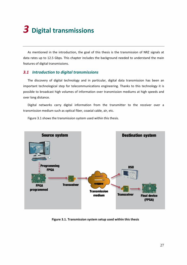
3 Digital transmissions
As mentioned in the introduction, the goal of this thesis is the transmission of NRZ signals at
data rates up to 12.5 Gbps. This chapter includes the background needed to understand the main
features of digital transmissions.
3.1 Introduction to digital transmissions
The discovery of digital technology and in particular, digital data transmission has been an
important technological step for telecommunications engineering. Thanks to this technology it is
possible to broadcast high volumes of information over transmission mediums at high speeds and
over long distance.
Digital networks carry digital information from the transmitter to the receiver over a
transmission medium such as optical fiber, coaxial cable, air, etc.
Figure 3.1 shows the transmission system used within this thesis.
Figure 3.1. Transmission system setup used within this thesis

28
The source system consists of a digital data source and a transmitter. In our system, the digital
data source is the FPGA once it has been programmed using the code developed in HDL. A
transceiver embedded in the FPGA is used to send the data through an SMA cable (transmission
medium) to the receiver. After the transmission medium, the data can follow two different paths.
First, using the Digital Storage Oscilloscope (DSO) as a receiver if what is desired is to study the
transmitted signal. Second, returning data to the FPGA again. In this case, the data is received in the
transceiver, which reconverts the incoming data into the original form, adjusts the nominal voltage
required by the destination and routes the signal into the FPGA again. The FPGA is responsible for
completing the final task entrusted (e.g. realize a logic operation between the bits obtained to show
the information in its screen).
As said before, digital data transmission carries digital information, which means that the
information is expressed as a sequence of 1’s and 0’s. However, the transmission medium does not
support that kind of data. For this reason, the binary information must be turned into signals with
different electrical levels. For example, the transmitter can set one state for the bit 1 and another
different state for the bit 0. Therefore, the function of the transmitter is to modify the digital data
adapting it to be carried over the physical medium, as shown in Figure 3.2. On the other end of the
communication system, the receiver reconverts this data into the original form to be processed by
the final device.
The process implemented in the transmitter is called line encoding and it is chosen based on the
transmission medium type. For example, modern applications require carrying information at high
data rates over fibers and cables. Consequently, high bandwidths are needed. Some types of
encoding can reduce the bandwidth needed by the transmitted pulses. Moreover, error free needs
to be ensured after recovering the transmitted signal at the receiver side.
Even though new technology is used to implement enhanced equipment functionalities, the
newest devices are not yet capable to detect and/or correct errors received. For this reason, all the
machines need to follow very specific protocols to ensure the correct and complete communication
Figure 3.2. Example of binary encoding in a digital transmission system

29
between devices. Consequently, the type of encoding is chosen based on which protocol the
communication line supports.
3.2 Non-return-to-zero (NRZ) and multilevel encoding
The simplest way to encode digital data is using different voltage levels for each bit sent value
(i.e. 0 and 1). This is called binary encoding. The codes that follow this method keep the constant
voltage level throughout the period of the bit. The most common binary encoding is Non-return-to
zero (NRZ) code, where bit 1 is represented as a positive voltage, and bit 0 as a negative voltage. In
addition, they make an efficient use of the bandwidth defined as the inverse of the length of the
duration of the pulses [12]. This means that these codes create long duration pulses compared to
other codes, i.e. there are fewer transitions between bits 1’s and 0’s. However, since it is not
possible to control the amount of 1’s and 0’s of the message, there is the possibility of long
sequences of consecutive 0’s or 1’s. These long sequences cause two problems. Firstly, long
sequences imply that the voltage levels which are called DC levels, are more sensitive to
attenuation for many transmission mediums. Secondly, when the same voltage level appears for a
long time, the receiver cannot distinguish how many bits are in that level, causing synchronization
problems between receiver and transmitter.
Figure 3.3. NRZ encoding in a digital transmission. A) original data before encoding B) data
after NRZ encoding C) data at the receiver

30
Figure 3.3 presents a simple example of the NRZ encoding in a digital transmission. Figure 3.3A
shows the original data before being encoded, i.e. the information that must be transmitted is
represented as a sequence of 1’s and 0’s. Afterwards, transmitter encodes the digital data using an
NRZ code (Figure 3.3B). The encoded signal is then sent to the receiver through the transmission
channel. The information reaches the receiver as shown Figure 3.3C due to the distortions such as
noise, attenuation and propagation delays that transmission medium introduces. Figure 3.3C
depicts the effect related to transmission of the long sequence of zeros. The long sequence of 0’s
introduces an additional DC signal obtaining a value close to 0 at the receiver side and consequently
increasing the possibility of creating an error.
Although binary codes are the easiest way of encoding, they are not the best solution for some
transmission mediums. In fact, due to the limitations explained above, they are not appealing for
ultra high speeds transmission applications [13].
Usually, multilevel codes are used for high speed transmission applications. These codes can be
created from the combination of two or more NRZ signals. Multilevel codes encode more than 1 bit
of information in each symbol and therefore, obtaining more than two different levels. The simplest
multilevel coding would result in one symbol that carries two bits.
In the simplest multilevel code, two consecutive bits of the data stream are taken together in
order to encode the information, thus creating a symbol consisting in two bits. Hence, the four
possible combinations shown in Figure 3.4A exist, presenting four different voltage levels. If the
multilevel method is applied to the stream 10 11 01 11 00 00 10 , the following encoded signal is
obtained (Figure 3.4B).
Comparing NRZ encoding (Figure 3.3B) and multilevel encoding (Figure 3.4), it can be deduced
that higher data rates are achieved using multilevel codes since each transmitted symbol
corresponds to 2 bits of information instead of 1. However, the bit error rate (BER) is higher in the
multilevel approach than in NRZ codes since spacing between voltage levels is reduced increasing
the probability of mistaking between them. The Shannon-Hartley theorem must be considered to
Figure 3.4. Multilevel code generation. (A) levels generated for 2 bits multilevel code (B) example
of multilevel encoding
A B

31
choose the correct encoding code. According to this theorem there is a theoretical limit of the
maximum amount of data that can be transmitted over a channel with a specific bandwidth [14].
C = 2Blog2M
where,
C = capacity of information in bits per second
B = channel bandwidth in Hertz
M = Number of possible states per symbol
Finally, the features of the binary codes and multilevel codes are summarized in Table 3.1. To
compare one code to another, it has been assumed that both have been applied in the same digital
data system.
Table 3.1 Comparison between Binary codes and Multilevel codes
3.3 Synchronization
The successful transmission depends not only on the good choice of the encoding at the
transmitter but also on the correct decoding into the receiver, i.e. the restoration of the
information to its original form. To achieve this, the receiver needs to know when each received bit
starts and finishes. This process is called synchronization. To achieve the bit synchronization, the
receiver samples the encoded signal at a speed specified by its internal clock. The receiver clock
must be synchronized with the transmitter clock; thereby bits start and finish at the expected
moments. Clocks are essential devices for the efficient functioning of digital transmission systems.
To decode successfully the received signal, one might think that it is enough to sample the signal
per bit period. In this way, the receiver can decide if the symbol corresponds to a 1 or a 0 depending
on whether, in the NRZ case, the voltage observed is positive or negative. However, the sampling
time cannot be chosen randomly. For example, if the sampling time is chosen at the beginning or at
the end of the pulse, there is higher probability of losing or doubling data compared to a sampling
time in the middle of the pulse. This occurs because real channels produce distortions to the

32
transmitted signal causing, consequently, fluctuations in the sampling time chosen previously.
These variations are usually random and they are called jitter effect. Jitter effect can produce the
incorrect decoding of the transmitted information when the receiver clock works at slow speed.
Figure 3.5 shows how jitter effect causes an error to the recovered signal.
Figure 3.5 Example of erroneous signal recovery due to jitter effect
One solution to reduce this effect is to increase the sampling rate at the receiver and thus, avoid
error accumulation (Figure 3.6) ensuring the detection of every transition from 0 to 1 and vice
versa.
Figure 3.6 Example of sampling at high speed
Nevertheless, if the synchronization between transmitter and receiver is not very accurate, it is
very difficult to decipher how many bits there are in long sequences of consecutive 1’s or 0’s. To
more easily control and try to avoid having these problematic sequences, the entire stream is split
in small independent sections. Limiting the amount of consecutive transmitted bits at a time, the
receiver is forced to resynchronize at the beginning of each group of bits. Each group of bits of
information transmitted consecutively is called word. The number of bits per word is set by the
protocol used in the transmission.
The word synchronization can be gotten through synchronous or asynchronous data
transmission. In both cases the goal is to accurately recognize the moment when a word starts and
when it finishes.
33
In asynchronous transmission, each word is sent at different times. In this case, the receiver
cannot control the space between consecutive words because this space depends on the channel.
For asynchronous systems, word synchronization is achieved by adding three control bits to every
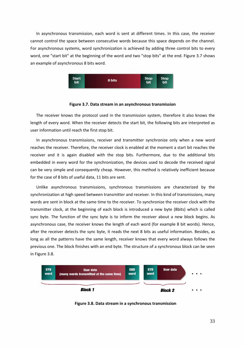
word, one "start bit" at the beginning of the word and two "stop bits" at the end. Figure 3.7 shows
an example of asynchronous 8 bits word.
Figure 3.7. Data stream in an asynchronous transmission
The receiver knows the protocol used in the transmission system, therefore it also knows the
length of every word. When the receiver detects the start bit, the following bits are interpreted as
user information until reach the first stop bit.
In asynchronous transmissions, receiver and transmitter synchronize only when a new word
reaches the receiver. Therefore, the receiver clock is enabled at the moment a start bit reaches the
receiver and it is again disabled with the stop bits. Furthermore, due to the additional bits
embedded in every word for the synchronization, the devices used to decode the received signal
can be very simple and consequently cheap. However, this method is relatively inefficient because
for the case of 8 bits of useful data, 11 bits are sent.
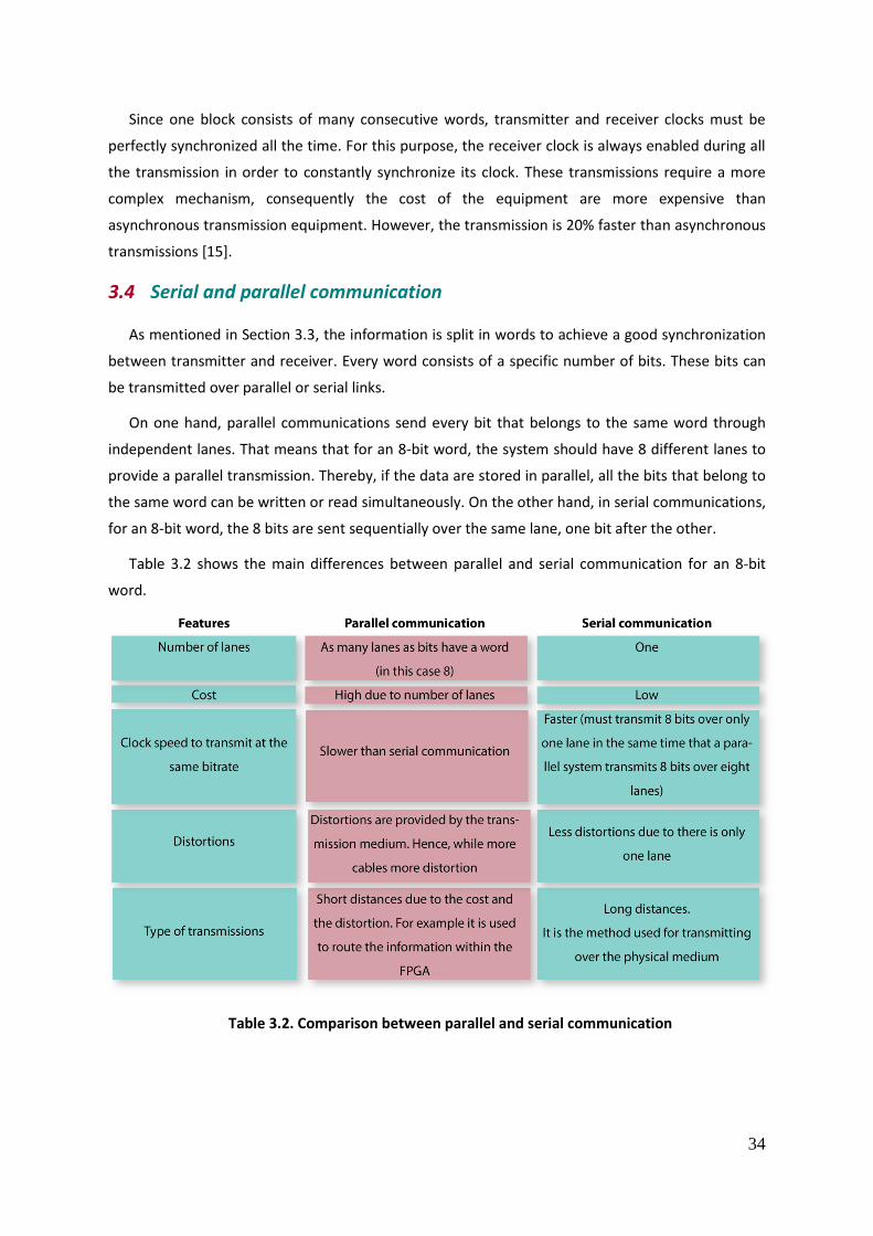
Unlike asynchronous transmissions, synchronous transmissions are characterized by the
synchronization at high speed between transmitter and receiver. In this kind of transmissions, many
words are sent in block at the same time to the receiver. To synchronize the receiver clock with the
transmitter clock, at the beginning of each block is introduced a new byte (8bits) which is called
sync byte. The function of the sync byte is to inform the receiver about a new block begins. As
asynchronous case, the receiver knows the length of each word (for example 8 bit words). Hence,
after the receiver detects the sync byte, it reads the next 8 bits as useful information. Besides, as
long as all the patterns have the same length, receiver knows that every word always follows the
previous one. The block finishes with an end byte. The structure of a synchronous block can be seen
in Figure 3.8.
Figure 3.8. Data stream in a synchronous transmission
34
Since one block consists of many consecutive words, transmitter and receiver clocks must be
perfectly synchronized all the time. For this purpose, the receiver clock is always enabled during all
the transmission in order to constantly synchronize its clock. These transmissions require a more
complex mechanism, consequently the cost of the equipment are more expensive than
asynchronous transmission equipment. However, the transmission is 20% faster than asynchronous
transmissions [15].
3.4 Serial and parallel communication
As mentioned in Section 3.3, the information is split in words to achieve a good synchronization
between transmitter and receiver. Every word consists of a specific number of bits. These bits can
be transmitted over parallel or serial links.
On one hand, parallel communications send every bit that belongs to the same word through
independent lanes. That means that for an 8-bit word, the system should have 8 different lanes to
provide a parallel transmission. Thereby, if the data are stored in parallel, all the bits that belong to
the same word can be written or read simultaneously. On the other hand, in serial communications,
for an 8-bit word, the 8 bits are sent sequentially over the same lane, one bit after the other.
Table 3.2 shows the main differences between parallel and serial communication for an 8-bit
word.
Table 3.2. Comparison between parallel and serial communication

35
36
4 Transceivers
In this project seven transceiver channels were programmed. Therefore, understanding the
work principles of transceiver devices is essential for us to be able to configure and control
them. This chapter explains how the transceivers control the signal transmission functionalities
such as synchronization, error detection and elimination of problematic bit sequences.
4.1 Introduction to transceiver devices
Although the concept of protocol was already introduced previously, it is worth going a little bit
more depth in this concept for a better understanding of the utilities of high-speed transceivers in
the field of new technologies. A protocol can be defined as a set of rules used by two different
systems within a communication network to share information between each other. Namely, they
are used in those applications that carry high amount of data from one device to another. Example
applications are: computational, communications, industrial etc. [16]. The protocol should be
chosen according to the physical medium of the digital transmission system, the transmission
requirements, the format of the data, the way of error detection and correction and the desired bit
rate, amongst others.
New protocols have emerged over the last years due to the need to obtain increased data
transmission rates within a limited bandwidth. For this reason, FPGAs with embedded high speed
transceivers becomes increasingly important. Consequently, FPGAs are commonly found as a part
of the physical interface of the newest protocols since high-speed transceivers can support the
most of the applications mentioned above [17].
A transceiver can be defined as a device that performs functions of both reception and
transmission of signals for high speed communications applications (hundreds of Mbps to Gbps)
[16]. The final reachable bit rate will depend on both the protocol chosen for the communication
and the capacity of the transceiver.
All the transceivers consist of two main blocks: Physical Coding Sub-layer (PCS) and Physical
medium attachment (PMA).
First of all, the PMA block is connected directly to the physical medium such as board traces,
backplanes, optical fibers, coaxial cables etc. [18]. The function of the PMA is to convert the
information from parallel data to serial data and vice versa.

37
Secondly, the PCS block is connected directly to the FPGA. On the transmitter path, its purpose is
to adapt the data coming from the FPGA to be transmitted over the physical medium. On the
receiver path, the function of this block is the opposite, i.e. to prepare data from the physical
medium to be accepted by the FPGA.
In the Stratix V FPGA high-speed transceivers architecture, PCS blocks of the transmitter and the
receiver can be programmed using three different configurations. They can be configured as
standard, 10G or PCI Express Gen3. Every PCS configuration can be combined with a specific PHY IP
core (Native PHY IP, Custom PHY IP or Low Latency PHY IP) which are responsible for enabling or
disabling of some parts of PCS module. These combinations enable the transceiver to support any of
the following communication protocols [19].
10GBASE-R and 10GBASE-KR
Interlaken
PCI Express Gen1, Gen2, and Gen3
CPRI and OBSAI
XAUI
Protocol customized by user
Each of these protocols support different physical mediums and different bit rates and must be
chosen depending on the user final target.
Figure 4.1 shows a simplified scheme of a transceiver where the PCS and PMA blocks of both the
transmitter and the receiver can be seen.
Figure 4.1. Main blocks and signals of a Stratix V transceiver

38
4.2 Architecture of high-speed transceivers
This section explains the high speed transceivers architecture embedded in a Stratix V FPGA. The
data to be transmitted is generated by a data pattern generator, which uses an NRZ encoding.
Hence, data is passed directly into the transceiver as soon as it is created [20].
As we shall see in Chapter 6, the 10G PCS configuration was chosen to perform all the designs
implemented in this thesis. Therefore, the PCS architecture will be explained focusing on 10G PCS
configuration.
4.2.1 Transmitter path
4.2.1.1 TX 10G Physical Coding Sub-layer configuration blocks
The TX 10G PCS consists of seven blocks: transmitter FIFO, Frame Generator, CRC-32 Generator,
64B/66B Encoder, Scrambler, disparity generator and transmitter Gearbox, as shown Figure 4.2. As
mentioned before, 10G PCS configuration can be combined with different PHY IP cores. Each
different combination can support different protocols. All mentioned protocols do not require all
the seven blocks of the PCS. Thus, some blocks that compose the PCS can be disabled depending on
the protocol implemented [19]. Every block will be explained in details below. The Interlaken and
10GBASE-R protocols, which use 10 G PCS configuration, are used as examples.

39
Figure 4.2. 10G transmitter PCS architecture showing the 10GBASE-R and Interlaken protocols paths

40
The transmitter FIFO (TX FIFO) is the first block that parallel data and control bits are passed
through when they reach the transmitter. So far, bits were synchronized according to the clock
system; therefore, the task of this module is to synchronize data to the transmitter’s internal clock
(refer to Section 4.3 for more information about clock architecture).
If the transceiver is configured for supporting Interlaken protocol the next block that data is
processed in is the Frame generator. The Frame Generator block encloses the 64 input bits (7 bytes
of data and 1 byte of word control) and attaches four control words to build the Interlaken Meta
Frame. These four new words are frame synchronizer, scrambler state, skip words, and diagnostic
word, as shown Figure 4.3.
Figure 4.3. Frame generator creating a Meta Frame
The function of the additional four control words are detailed in Table 4.1 [21].
Table 4.1. Functions of Diagnostic word, Skip word, Scrambler word and Synchronization word
[21]
Next module is a cyclic redundancy check 32 (CRC-32) generator and as in the previous module is
enabled only if the transceiver supports Interlaken protocol. The function of this module is to
calculate the checksum over all the bytes transmitted that come from the Frame generator. The
checksum applies a specific mathematical algorithm to all the data bits of the frame. CRC sets the
result into the diagnostic word of Meta Frame. That enables the receiver to check if any error
occurred during transmission.

41
If the transceiver supports 10G BASE-R protocol, data jump directly from transmitter FIFO to
64B/66B encoder block. This block is only enabled if transceiver supports this protocol. Its function
is to convert the 64 input bits, which come from of transmitter FIFO block, to 66 bits. By doing this,
enough transitions are ensured to allow the recovery of the internal transmitter clock at the
receiver path. The recovered clock synchronizes the receiver and the transmitter, allowing data
stream alignment in the receiver. Although in 10G PCS the 64B/66B encoders are used, they are not
the most common encoders. 8B/10B encoders are more common and they are used for example in
standard PCS configurations. However, 8B/10B encoders imply a 25% of overhead versus to 3% of
overhead from 64B/66B encoders [22]. Thanks to overhead reduction comparing to 8B/10B
encoding, 64B/66B encoding is used when transceiver is providing data transmissions rates higher
than 8.5 Gbps [19].
After 64B/66B encoder in the case of 10GBASE-R protocol and after CRC-32 generator for
Interlaken protocol, data is passed to Scrambler module. Data transmission systems do not have
control over transmitted bit stream. Consequently, some particular bit streams often appear, such
as long sequences of 1’s or 0’s. These particular sequences produce problems in the performance of
the transmitter such as excessive radiofrequency interferences, intermodulation, distortion or bit
synchronization error. The purpose of the scrambling module is to remove these particular
sequences of bits. Depending on the protocol configuration, the algorithm used for scrambling can
be different.
After the scrambler module, a random sequence of 1’s and 0’s is provided. Although the data
stream has been mixed previously, it does not ensure that sequences of consecutive bits of the
same value will not appear. Disparity Generator block is charged with monitoring the output of the
scrambler block and checks if any problematic sequence appears. The problematic words will be
inverted if anyone reaches to Disparity Generator in order to maintain neutral disparity, i.e. the
same number of 1’s than 0’s. Besides, in the Disparity Generator the bit 66 of the stream is inverted
to inform the receiver that a word inversion has occurred during the transmission path.
In 10G configuration for Interlaken and 10GBASE-R protocols the word wide allowed in the PMA
input is 40 bits. Hence, the function of the last block of PCS called Transmitter Gearbox is to adapt
the word wide that comes from the PCS to the word wide allowed by the PMA interface. That
means, the Transmitter Gearbox will have to change the 66 bits that it finds in its input to 40 bits
per word.
4.2.1.2 Transmitter Physical Medium Attachment blocks
After PCS module, the parallel data goes through the PMA module. The PMA is the last module
before the data gets into the physical medium.

42
The PMA is composed of a serializer and a transmitter buffer. Figure 4.4 depicts a block diagram
of the generic structure of a PMA within the transmitter.
The function of the transmitter serializer is to take multiple data line inputs and to condense the
system to a single output. Hence, the serializer transforms parallel data into serial data. To do this,
two different clocks are needed, one clock running at a slow speed for the parallel data and another
clock running at a high speed for the serial data. The final data rate over the link will depend on the
high speed serial clock as shown the example of Figure 4.5.
Figure 4.4. Transmitter PMA architecture
Figure 4.5. Example of converting parallel data to serial data

43
The last module that data passes through before go to the physical medium is called Transmitter
buffer. One of the functions of this module is to adapt the serial digital information to the standard
output (I/O pins) supported by the FPGA. Furthermore, as we already know, when a signal passes
through a communication channel it suffers attenuation, dispersion and noise. These three factors
make it more difficult to successfully recover the original signal sent from transmitter to the
receiver. Hence, the transmitter buffer is also responsible for ensuring that the minimum receiver
requirements are reached and thus, to improve the quality of the final transmission. For this
purpose, the transmitter buffer can manage the pre-emphasis feature and set the appropriate
voltage level of the NRZ signals at the output of the transmitter. This voltage level will be chosen in
an attempt to improve the quality of the signal that arrives at the receiver.
4.2.2 Receiver path
The function of the receiver is to return serial data to its original form to allow the FPGA to
interpret the information correctly. For this reason, almost all modules within the receiver perform
the inverse operation to the transmitter modules do.
4.2.2.1 Receiver Physical Medium Attachment blocks
When a serial data reaches the receiver from the physical medium, the first module that they
find is the PMA. The PMA consists of a receiver buffer, a clock and a data recovery unit (CDR), and a
deserializer. Figure 4.6 depicts a block diagram of the generic structure of the receiver PMA.
Figure 4.6. Receiver PMA architecture
Since in practice an ideal transmission channel does not exist, the received signal differs from
the original signal transmitted. The transmission medium decreases the signal-to-noise ratio (SNR)
of the signal and consequently increases the probability of error. For this reason, the receiver
system needs additional elements to compensate or reduce the impairments of the signal. For
instance, the receiver buffer has an equalizer available to eliminate or reduce the ISI effects.
Additionally, it is also responsible for setting the voltage required in the input of the receiver to the
arrival data supporting DC gain up to 8 dB [22].
44
The receiver CDR is responsible for extracting the clock embedded in the input data stream to
synchronize the receiver with the transmitter. The clock can be only recovered if the serial data
have enough transitions from 0 to 1 and from 1 to 0. Those transitions inform the CDR in which
moment the original clock transitions are taking place. This is the point when it reveals if the work
of the 64B/66B encoder in the transmitter path was successfully performed.
Additionally, CDR generates two more clocks from the recovered clock. One of the clocks
generated run at a high speed and another at a slow speed. These generated clocks will be used by
the receiver deserializer to change from the serial data to the parallel data (arranging of the original
data).
4.2.2.2 RX 10G Physical Coding Sub-layer configuration blocks
The 10G PCS RX consists of nine blocks: a receiver Gearbox, a block synchronizer, a disparity
checker, a descrambler, a frame synchronizer, a BER monitor, a 64B/66B decoder, a CRC-32 checker
and a receiver FIFO. As with transmitter PCS, some blocks are disabled according to which protocol
the transceiver is supporting. Figure 4.7 shows the architecture of the PCS in the receiver for
Interlaken and 10GBASE-R protocols, while Table 4.2 below explains the features of each individual
block.

45
Figure 4.7. 10G receiver PCS architecture showing the 10GBASE-R and Interlaken protocols paths

46
RX PCS block Features
Receiver Gearbox
Perform the inverse operation to the Transmitter Gearbox does.
It adapts the 40 bits word coming from the PMA to 66 bits required by
the receiver PCS.
Block synchronizer
Since data stream is serialized when they reach the receiver, block
synchronizer finds the word synchronization and performs the correct
align within the parallel data stream.
Disparity checker
Only it is enabled for Interlaken protocol.
Check bit 66 of each word to find out if it was inverted by the disparity
generator during the transmission. If yes, disparity checker places each
bit in its original position within the word.
Descrambler Perform the inverse operation to the scrambler in the transmitter does,
i.e. it returns the scrambled bits to its original position.
Frame synchronizer
Only it is enabled for Interlaken protocol.
Its task is to synchronize the Meta Frame within the receiver by
detecting each control word (synchronizer, scrambler state, skip words,
and diagnostic word). It is assumed a synchronized system when 4
consecutive correct Meta frames (sync control word) are detected. On
the other hand it is assumed that system has lost the synchronization if
3 consecutive incorrect Meta frames are detected [18][19].
BER monitor
Only it is enabled for 10GBASE-R protocol.
Once synchronization is reached by the block synchronizer, BER monitor
starts to count how many times receiver loses the synchronization
within a period of 125 s [22].
64B/66B Decoder
Only it is enabled for 10GBASE-R protocol.
Perform the inverse operation to 64B/66B encoder located at the
transmitter path does.
It converts the 66 bits encoded to 64 bits of data and 1 byte of control.
CRC-32 checker
Only it is enabled for Interlaken protocol.
Perform the inverse operation to CRC-32 generator located at the
transmitter path does.
It calculates the checksum over all the bytes that reach the CRC-32
checker and compares the result with the checksum calculated by the
transmitter located in the diagnostic word of the Meta frame.
If the value is not the same means that errors have occurred.

47
Table 4.2. Features of receiver PCS blocks
4.3 Clocking Architecture
All the signals within a transceiver are controlled by clocks without which the transceiver would
not work. A simplified scheme of the clocking architecture of the transceiver is depicted in Figure
4.8.
Figure 4.8. Transceiver clocking architecture
One of the most troublesome effects when working with clocks is the jitter, which affects the
final transmission. Let us recall briefly what jitter is. Jitter is a phenomenon caused by the slightly
deviation on the accuracy of clock signals when digital data are transmitted. This lack of accuracy
has a negative impact on the performance of the system. The system clock of the FPGA does not
have the appropriate specifications to ensure a good transmission through the high speed
transceivers. This is because the system clock works at slow speed (possible frequencies are 25,
100, 125 or 200 MHz) [9]. Consequently, in order to get acceptable jitter values when the
transceiver works at high speeds, the transceiver channels have their particular PLLs. PLL clocks
generate all the internal clocks required by the transmitter to obtain a final high quality
transmission.
The transmit PLL use a reference clock to generate the serial clocks (programmable frequency
range are from 10 MHz to 1.4 GHz) [9]. At the receiver, the CDR uses the reference clock to recover
the clock to synchronize the receiver with the transmitter.
Receiver FIFO
Perform the inverse operation to Transmitter FIFO located at the
transmitter path does.
Receiver FIFO is the last block that data pass through before go into the
FPGA. This block allows the synchronization of the data with the clock
system of the FPGA.

48
The transmit PLL can be configured as auxiliary transmit PLL (ATX), clock multiplier unit PLL
(CMU) or fractional PLL [23]. Table 4.3 summarizes the main differences between them.
Table 4.3. Differences between ATX PLL, CMU PLL and fPLL [23][23]
Every transceiver channel within a transceiver block (six transceiver channels) has a local clock
divider except channel 1 and 4. Channels 1 and 4 have a central clock divider; however, they can
also work as local clock dividers. The function of these internal clocks is to provide the parallel clock
to each channel from the serial clock. The way to create the parallel clock depends on the
configuration of the transceiver clocking (bonded clocking or non-bonding clocking). When the
channel is configured as a bonded channel, all the parallel clocks are generated by a central clock
divider and that means generating the same parallel clocks for all channels. However, in non-
bonded configuration, the frequency of the parallel clock is generated by the local clocks divider
located in each transceiver channel. That means the possibility to get one different parallel clock
frequency in each transceiver channel (i.e. different bit rates).
4.4 Eye diagram
All the digital components of the on-board transceiver and all the transmission media affect the
transmitted signal. For this reason, it is very important to in-depth study the quality of the
transmission system to be sure that the signal fulfills to minimum requirements for a good recovery.

49
Therefore, it is essential to perform a pulse wave analysis to observe their shape, jitter, noise,
amplitude etc. All these parameters can be studied in the eye diagram.
The eye diagram shows all the bits within the same temporal window. That means, the data flow
consisted in 1’s (+V) and 0’s (-V), in the case of NRZ encoding, is cut off at constant bit period-
intervals to continue by overlying to each other. Figure 4.9 shows how an eye diagram is formed
from a data stream and all the parameters that can be studied from it.
Figure 4.9. Generation of an eye diagram from a NRZ stream data and parameters of the eye
diagram
One Level: It corresponds to the average of the level of logic one.
Zero Level: It corresponds to the average of the level of logic zero.
Rise Time and Fall Time: Once the zero and one logic have been set, Rise time corresponds to
the interval time between 10% and 90% from the maximum amplitude of the pulse (one level)
[25]. In contrast, the Fall time is calculated as Rise time but from zero level. These measures
inform about how the system responds to high data rates.
Eye Crossing Percentage: The eye crossing percentage is calculated as follows:
–
– [25]
where crossing level is the position where the eye is opened and subsequently closed. The eye
crossing indicates if the original signal was affected by some distortions during the transmission
(pulse broadening or pulse compression).
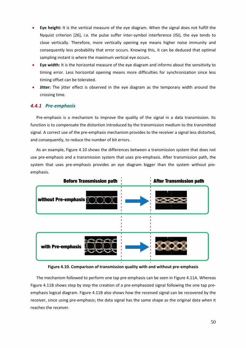
50
Eye height: It is the vertical measure of the eye diagram. When the signal does not fulfill the
Nyquist criterion [26], i.e. the pulse suffer inter-symbol interference (ISI), the eye tends to
close vertically. Therefore, more vertically opening eye means higher noise immunity and
consequently less probability that error occurs. Knowing this, it can be deduced that optimal
sampling instant is where the maximum vertical eye occurs.
Eye width: It is the horizontal measure of the eye diagram and informs about the sensitivity to
timing error. Less horizontal opening means more difficulties for synchronization since less
timing offset can be tolerated.
Jitter: The jitter effect is observed in the eye diagram as the temporary width around the
crossing time.
4.4.1 Pre-emphasis
Pre-emphasis is a mechanism to improve the quality of the signal in a data transmission. Its
function is to compensate the distortion introduced by the transmission medium to the transmitted
signal. A correct use of the pre-emphasis mechanism provides to the receiver a signal less distorted,
and consequently, to reduce the number of bit errors.
As an example, Figure 4.10 shows the differences between a transmission system that does not
use pre-emphasis and a transmission system that uses pre-emphasis. After transmission path, the
system that uses pre-emphasis provides an eye diagram bigger than the system without pre-
emphasis.
Figure 4.10. Comparison of transmission quality with and without pre-emphasis
The mechanism followed to perform one tap pre-emphasis can be seen in Figure 4.11A. Whereas
Figure 4.11B shows step by step the creation of a pre-emphasized signal following the one tap pre-
emphasis logical diagram. Figure 4.11B also shows how the received signal can be recovered by the
receiver, since using pre-emphasis; the data signal has the same shape as the original data when it
reaches the receiver.

51
Figure 4.11. Pre-emphasis system. A) One-tap pre-emphasis logical representation. B) One-tap
timing diagram [27]
A
B

52

53
5 Experimental designs
This chapter presents all the designs that have been performed in order to program seven 12.5
Gbps transceiver channels available through SMA connectors. These transceivers are integrated in
the Stratix V FPGA produced by Altera [refer to Annex A for more information about Kit Stratix V
FPGA (5SGXEA7K2F40C2N)]. All the designs presented in this thesis have been created via Quartus II
v 12.1 software developed by Altera. This specialized software allows creating designs through the
creation of logic circuits or through a specific programmable language called Hardware Description
Language (HDL). Once the design has been created it can be implemented in the FPGA. The designs
shown in this chapter have been achieved combining the two options of creation: block diagrams
and VHDL or Verilog programming languages. The transceivers configuration was performed in
order to provide the best jitter performance and the minimum latency in order to offer the broad
operational frequency range (1 Gbps to 12 Gbps) [19].
5.1 Configuration of one transceiver channel transmitting up to 12.5 Gbps
bit rate using PRBS 7, 15, 23 or 31
The first design achieved was a single transceiver channel transmitting NRZ signals with a bit rate
up to 12.5 Gbps. This design was created exclusively in Qsys. Qsys is the recently added tool to
Quartus. This new tool allows to easily interconnect different blocks within a design to each other
without having to write the connections manually using the hardware programming language. The
communication between components within a Qsys system is performed through standard
interfaces called Avalon interfaces. Each component of the design has one or more Avalon
interfaces. The Avalon interfaces function is to allow the transmission of high speed data between
components and also write and read from the registers. The Avalon interfaces that have been used
in the implemented designs in this thesis are summarized below [28]:
Avalon Streaming Interface (Avalon-ST): permits the unidirectional transmission of stream data
from source to sink connections.
Avalon Memory Mapped Interface (Avalon-MM): permits the communication with the host,
allowing the master connection to write and read from/to a slave connection.
Avalon Conduit Interface: some signals do not need to be connected to another Avalon
interface, or sometimes they need to be connected to an FPGA pin or to another component
that has been created outside of Qsys. Those signals can be stuck or exported when its interface
is defined as conduit.
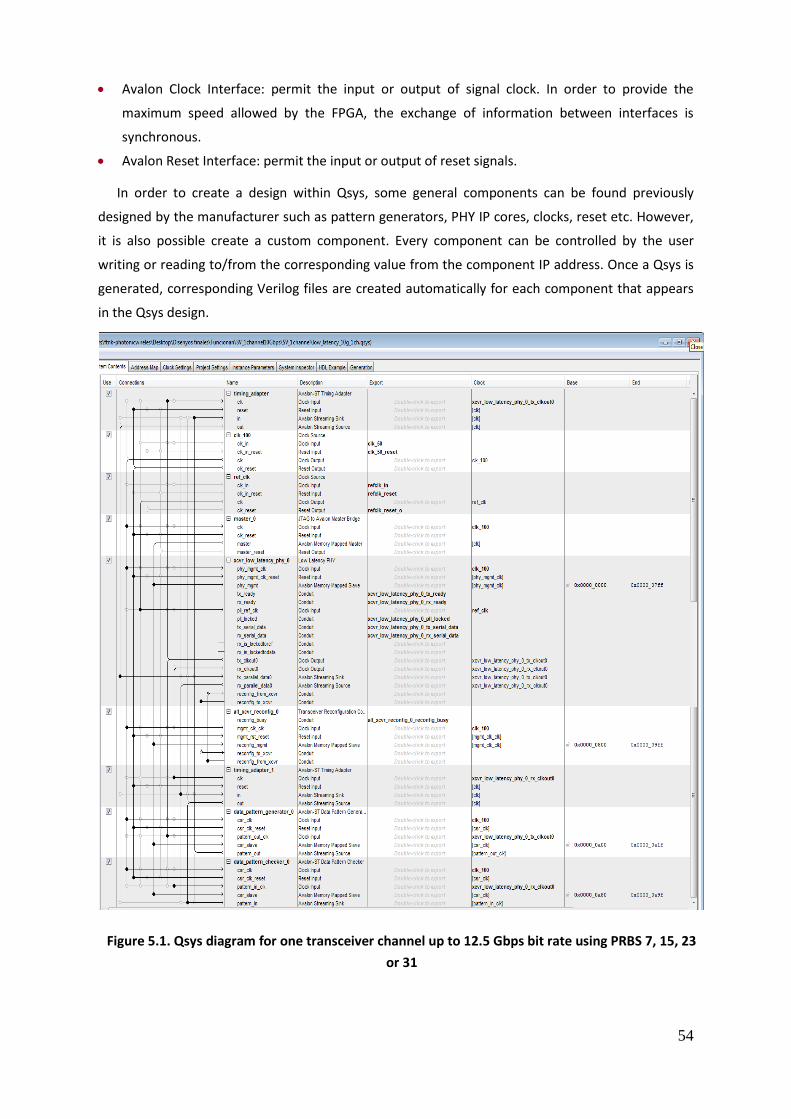
54
Avalon Clock Interface: permit the input or output of signal clock. In order to provide the
maximum speed allowed by the FPGA, the exchange of information between interfaces is
synchronous.
Avalon Reset Interface: permit the input or output of reset signals.
In order to create a design within Qsys, some general components can be found previously
designed by the manufacturer such as pattern generators, PHY IP cores, clocks, reset etc. However,
it is also possible create a custom component. Every component can be controlled by the user
writing or reading to/from the corresponding value from the component IP address. Once a Qsys is
generated, corresponding Verilog files are created automatically for each component that appears
in the Qsys design.
Figure 5.1. Qsys diagram for one transceiver channel up to 12.5 Gbps bit rate using PRBS 7, 15, 23
or 31

55
Figure 5.1 shows the created Qsys diagram for the configuration of one transceiver channel with
data rate up to 12.5 Gbps and with choice of Pseudorandom bit sequence (PRBS) 7, 15, 23 or 31.
PRBS pattern is a sequence of random bits of 1’s and 0’s. Due to the randomness of the
sequence, they can be considered equivalent to noise. Noisy signals are more difficult to recovery
by the receiver since they are very sensitive to transmission errors. Therefore, PRBS patterns can be
considered as the worst case test pattern. Consequently, if the transmission system can recover the
worst case, this means that the transmitter can transfer a good signal. A PRBS-X consists of a
sequence of 2x - 1 randomness bits before the same sequence starts to repeat again.
Qsys diagram allows one to see all blocks of the design, the interfaces of each component and
also the interconnections between them. Every Qsys component will be explained in detail below.
The main block of the design to configure a transceiver is the PHY IP core. As mentioned in the
chapter 3, three choices exist: Native PHY IP, Custom PHY IP or Low Latency PHY IP. Low Latency
PHY IP was chosen for implement the designs because it is the PHY IP core that provides the
smallest delay in the datapath. Consequently, the only option to get the maximum data rate
allowed by these transceivers (12.5 Gbps) [19].
Figure 5.2 shows the Low Latency PHY core Qsys component that was configured and its
interfaces.
Figure 5.2. General window of Low Latency PHY core block
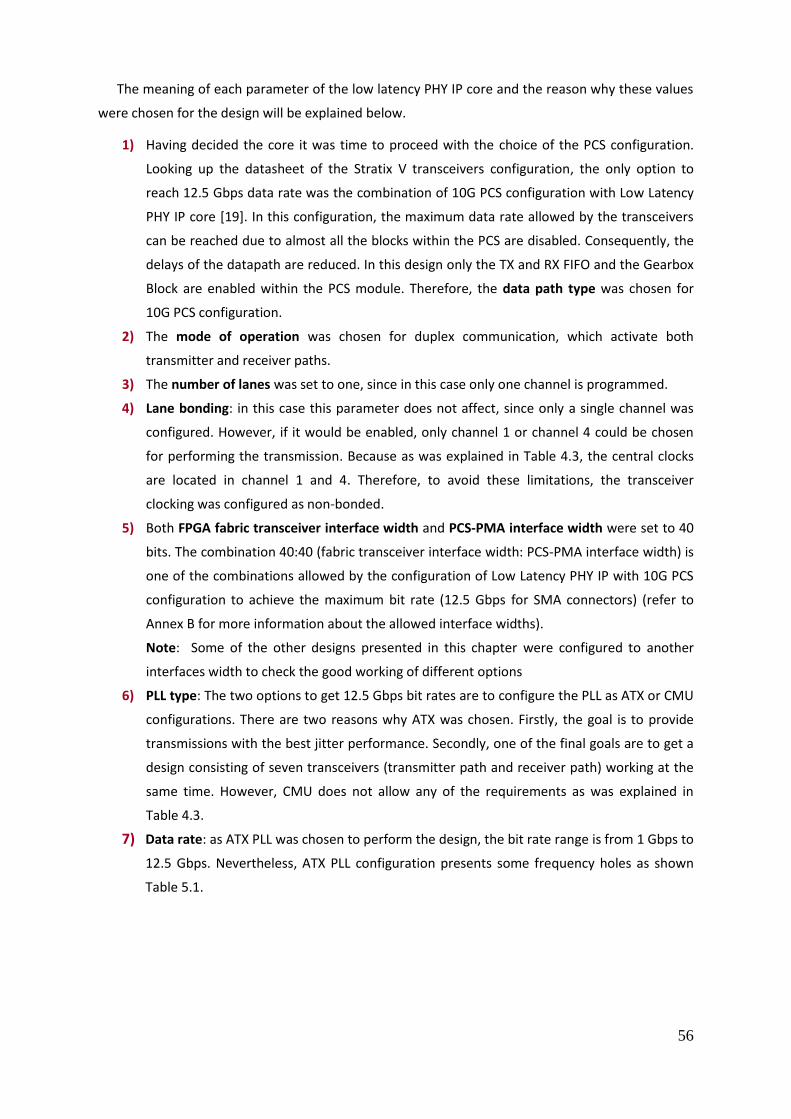
56
The meaning of each parameter of the low latency PHY IP core and the reason why these values
were chosen for the design will be explained below.
1) Having decided the core it was time to proceed with the choice of the PCS configuration.
Looking up the datasheet of the Stratix V transceivers configuration, the only option to
reach 12.5 Gbps data rate was the combination of 10G PCS configuration with Low Latency
PHY IP core [19]. In this configuration, the maximum data rate allowed by the transceivers
can be reached due to almost all the blocks within the PCS are disabled. Consequently, the
delays of the datapath are reduced. In this design only the TX and RX FIFO and the Gearbox
Block are enabled within the PCS module. Therefore, the data path type was chosen for
10G PCS configuration.
2) The mode of operation was chosen for duplex communication, which activate both
transmitter and receiver paths.
3) The number of lanes was set to one, since in this case only one channel is programmed.
4) Lane bonding: in this case this parameter does not affect, since only a single channel was
configured. However, if it would be enabled, only channel 1 or channel 4 could be chosen
for performing the transmission. Because as was explained in Table 4.3, the central clocks
are located in channel 1 and 4. Therefore, to avoid these limitations, the transceiver
clocking was configured as non-bonded.
5) Both FPGA fabric transceiver interface width and PCS-PMA interface width were set to 40
bits. The combination 40:40 (fabric transceiver interface width: PCS-PMA interface width) is
one of the combinations allowed by the configuration of Low Latency PHY IP with 10G PCS
configuration to achieve the maximum bit rate (12.5 Gbps for SMA connectors) (refer to
Annex B for more information about the allowed interface widths).
Note: Some of the other designs presented in this chapter were configured to another
interfaces width to check the good working of different options
6) PLL type: The two options to get 12.5 Gbps bit rates are to configure the PLL as ATX or CMU
configurations. There are two reasons why ATX was chosen. Firstly, the goal is to provide
transmissions with the best jitter performance. Secondly, one of the final goals are to get a
design consisting of seven transceivers (transmitter path and receiver path) working at the
same time. However, CMU does not allow any of the requirements as was explained in
Table 4.3.
7) Data rate: as ATX PLL was chosen to perform the design, the bit rate range is from 1 Gbps to
12.5 Gbps. Nevertheless, ATX PLL configuration presents some frequency holes as shown
Table 5.1.

57
Table 5.1. Frequency holes of ATX PLL [29]
Therefore, if some of the bitrates out of these ranges were achieved, the PLL type must be
changed to CMU PLL.
8) Input clock frequency:
Once the bit rate was set, Qsys chooses automatically the best option for the input clock
frequency. This input clock frequency is calculated following the next formula using the values of
Table 5.1:
where, n is any positive integer for high bit rates or 1 divided by any positive integer for low bit
rates. However, n must be chosen to achieve a result allowed by the PLL (from 100 MHz to 710
MHz) [33].
In this particular case the bit rate is 12500 Mbps, therefore:
Figure 5.3 shows a screenshot of the additional options window of the Low Latency PHY.
- Tx_coreclkin and rx_coreclkin allow the user choose the
parallel clock to run the parallel data, for instance an fPLL.
These parameters must be enabled for 50:40 and 64:32
configurations [30]. They are disabled because in this
design was used 40:40 widths.
- TX bitslip and RX bitslip allow a manual word alignment
in bitslip mode instead of use the high speed serial clock
and low speed parallel clock recovered from the received
data. In this particular case is used the default mode [31].
- Embedded reset controller is enabled by default. Its
function is to reset the PCS and PMA blocks of the
transceiver. In case of more than one PLL is used in a single
PHY IP core, the reset must be external [32].
Figure 5.3. Additional options
window of Low Latency PHY core
block
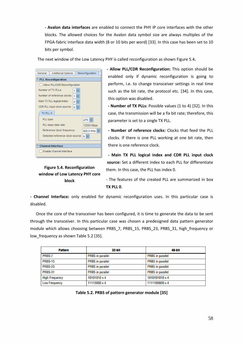
58
- Avalon data interfaces are enabled to connect the PHY IP core interfaces with the other
blocks. The allowed choices for the Avalon data symbol size are always multiples of the
FPGA-fabric interface data width (8 or 10 bits per word) [33]. In this case has been set to 10
bits per symbol.
The next window of the Low Latency PHY is called reconfiguration as shown Figure 5.4.
- Allow PLL/CDR Reconfiguration: This option should be
enabled only if dynamic reconfiguration is going to
perform, i.e. to change transceiver settings in real time
such as the bit rate, the protocol etc. [34]. In this case,
this option was disabled.
- Number of TX PLLs: Possible values (1 to 4) [32]. In this
case, the transmission will be a fix bit rate; therefore, this
parameter is set to a single TX PLL.
- Number of reference clocks: Clocks that feed the PLL
clocks. If there is one PLL working at one bit rate, then
there is one reference clock.
- Main TX PLL logical index and CDR PLL input clock
source: Set a different index to each PLL for differentiate
them. In this case, the PLL has index 0.
- The features of the created PLL are summarized in box
TX PLL 0.
- Channel Interface: only enabled for dynamic reconfiguration uses. In this particular case is
disabled.
Once the core of the transceiver has been configured, it is time to generate the data to be sent
through the transceiver. In this particular case was chosen a predesigned data pattern generator
module which allows choosing between PRBS_7, PRBS_15, PRBS_23, PRBS_31, high_frequency or
low_frequency as shown Table 5.2 [35].
Table 5.2. PRBS of pattern generator module [35]
Figure 5.4. Reconfiguration
window of Low Latency PHY core
block

59
The interface width of the pattern generator module where data stream comes out (Avalon-ST
source) must be 10 bits to communicate with Avalon-ST sink of the Low Latency PHY (Avalon data
interface = 10 bit per symbol). However, the valid values allowed by the pattern generator interface
are 32 or 40 bits [35]. This forces to use a time adapter, which divides the data per 2 or 4. The time
adapter adapts the Avalon-ST source width to the Avalon-ST sink width [35]. Therefore, if the
Avalon_ST sink width of the pattern generator is set to 40 bits and the timing adapter is configured
to divide by 4, it gets a 10 bit width.
The connections between pattern generator and low latency PHY IP can be seen in the Qsys
diagram (Figure 5.1). The pattern_out of the pattern generator is connected to the input of the
timer adapter, which changes the width of the data and sends the new stream from its output to
tx_parallel_data0 of the low_latency_phy. In the Qsys diagram it can be seen also that the clock of
the timing adapters is running according to the low speed parallel clock created in the transceiver as
expected.
In the receiver path, a pattern checker module was connected. The pattern checker module
knows the PRBS that was generated and any errors that occur are reported to the user. The
interfaces widths allowed by the pattern checker are the same as the pattern generator; therefore
another timing adapter was needed for adapting the interfaces.
In the Qsys design also appears a reconfiguration controller block (alt_xcvr_reconfig_0). This
block controls all the blocks within a transceiver. Therefore, it is the component responsible to
perform dynamic reconfiguration of the PCS and the PMA modules or the PLLs. Although this
transceiver design does not use any of these reconfigurations, it is necessary to add this block in the
Stratix V transceivers designs where the receiver path is enabled [36].
The number of reconfiguration interfaces needed is indicated on the bottom of the PHY IP core
window (see Figure 5.2). In this design a single transceiver channel with one PLL was configured,
consequently, 2 reconfiguration interfaces were needed as shown Figure 5.5 (one for the
transceiver channel and one for the transmit PLL).
Figure 5.5. Reconfiguration controller block options
The optional interface grouping specifies how reconfiguration interfaces should be grouped in
order to perform a design with more than one PHY IP core. All the reconfiguration interfaces of the
Low Latency PHY and the reconfigurations controller interfaces are connecting each other as can be

60
seen in Qsys diagram (Figure 5.1). However reconfig_busy interface was exported out of Qsys.
When this signal asserted means the reconfiguration is in progress.
Regarding the clock configurations, two clocks were created. The system clock (clk_100) driving
all the blocks outside the transceiver was set to 100 MHz (default value), while the reference clock
(ref_clk) which is connected to the PLL interface of the Low Latency PHY was set to 625MHz.
Finally, a last block called Jtag to Avalon Master bridge was instantiated in Qsys. As its name
suggest is a bridge between the host and the different modules of the design to be able to control
them. Thanks to this block some orders can be sent to the reconfiguration controller or read from
the checker generator slave interface to check if any error during the transmission happens. These
reads and writes can be controlled from the system console through Tcl programming language
commands. By writing a correct Tcl command in the system console, it is possible to write to and
read from the correct IP address of the desired block and therefore control it. Nevertheless, if all
the blocks of the design are connected in Qsys like in this case, the Transceiver Toolkit application
can be used to control the signals. The Transceiver Toolkit uses a graphical interface instead of the
Tcl language. Transceiver toolkit creates a link for each configured channel to control both the
transmitter and the receiver paths. For the transmitter link of the transceiver, this tool allows
changing between the different PRBS. Moreover, it also allows adding pre-emphasis taps to
improve the quality of the transmitted signal at real time. For the receiver path is possible the study
of the BER of the received data, controlling the equalization and even simulate the eye diagram as
show Figure 5.6.
Figure 5.6. Eye diagram simulation Transceiver Toolkit
In the Qsys diagram (Figure 5.1) also it can be seen that some signals have been exported in
order to connect them to the final pins of the FPGA. These final connections were performed in the
main program Quartus II. The specific wires and connections between modules were written using
Verilog code (see Annex C to see the top level Verilog code). The final interfaces then were
connected to the properly FPGA PINS. The clk_100 was connected to the system clock PIN of the
FPGA (PIN AV_7), the ref_clk was connected to one of the reference clock pins within the block
where the transceiver channel chosen (channel 0) was located (PIN AC_32). Finally, the interfaces

61
where the serial data come out were connected to the SMA connectors. For the transmitter path,
the tx_serial_data signal was connected to PIN Y_34 (channel 0) and for the receiver path,
rx_serial_data signal was connected to PIN AA_36 [9].
Refer to Annex D to see the block diagram of the design.
5.2 Configuration of seven transceiver channels transmitting at the same
bit rate up to 12.5 Gbps using PRBS 7, 15, 23 or 31
The second created design was composed of seven transceiver channels that transmit at the
same bit rate simultaneously. This design was also exclusively created in Qsys system. Below will be
explained the differences regarding to the one transceiver channel configuration design explained
above.
Low latency PHY IP
1) The number of lanes is seven. One for each transceiver channel.
2) FPGA fabric transceiver interface width and PCS-PMA interface width have been set to
64 bits, to test another valid combination according to the datasheet (refer to Annex B)
3) Avalon data symbol was set to 8 (multiple of 64).
4) The number of PLLs and reference clocks were set to 1, since the seven channels are
working at the same bit rate.
5) On the bottom of the low latency PHY IP informs that 14 reconfiguration interfaces were
needed since we are using non-bonded configuration. Therefore, it was necessary 7
interfaces for the transceiver channels (one per each channel) and seven interfaces for
the transmit PLL. The transmit PLL needs 7 reconfiguration interfaces because 7 parallel
clocks are generate from it (non-bonded configuration).
Reconfiguration controller
The number of reconfiguration interfaces was set to 14 and not interfaces grouping were
needed because there is only one PHY IP core.
Pattern generator, pattern checker and timing adapters
Seven different pattern generators were created to feed the transmitter path of each transceiver
channel. Creating one pattern generator per channel allows transmitting different PRBS through the
different channels if it is desired. Furthermore, each receiver path also was associated a pattern
checkers to control the errors. The Avalon_ST width was set to 32 bits and it was used a timing
adapter that divide by 4 in order to get 8 bits per symbol in the output (Avalon data symbol size
imposed by the PHY IP core).
Refer to Annex E to see the generated block diagram once the final pins were configured.
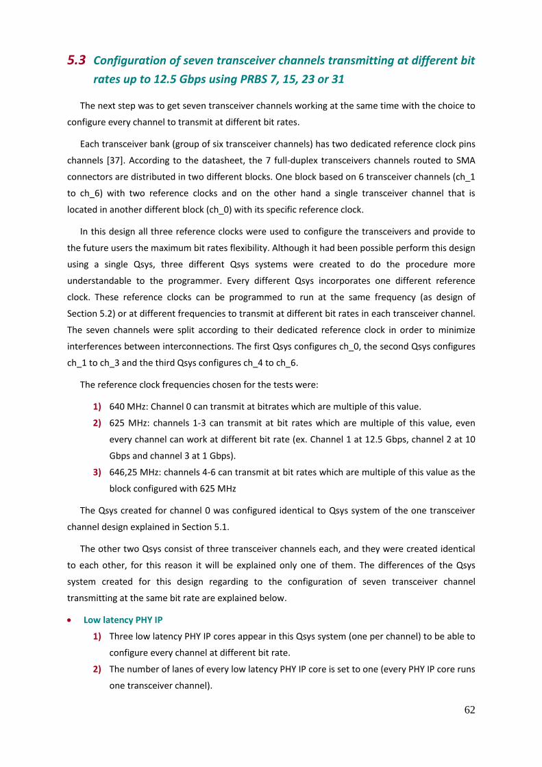
62
5.3 Configuration of seven transceiver channels transmitting at different bit
rates up to 12.5 Gbps using PRBS 7, 15, 23 or 31
The next step was to get seven transceiver channels working at the same time with the choice to
configure every channel to transmit at different bit rates.
Each transceiver bank (group of six transceiver channels) has two dedicated reference clock pins
channels [37]. According to the datasheet, the 7 full-duplex transceivers channels routed to SMA
connectors are distributed in two different blocks. One block based on 6 transceiver channels (ch_1
to ch_6) with two reference clocks and on the other hand a single transceiver channel that is
located in another different block (ch_0) with its specific reference clock.
In this design all three reference clocks were used to configure the transceivers and provide to
the future users the maximum bit rates flexibility. Although it had been possible perform this design
using a single Qsys, three different Qsys systems were created to do the procedure more
understandable to the programmer. Every different Qsys incorporates one different reference
clock. These reference clocks can be programmed to run at the same frequency (as design of
Section 5.2) or at different frequencies to transmit at different bit rates in each transceiver channel.
The seven channels were split according to their dedicated reference clock in order to minimize
interferences between interconnections. The first Qsys configures ch_0, the second Qsys configures
ch_1 to ch_3 and the third Qsys configures ch_4 to ch_6.
The reference clock frequencies chosen for the tests were:
1) 640 MHz: Channel 0 can transmit at bitrates which are multiple of this value.
2) 625 MHz: channels 1-3 can transmit at bit rates which are multiple of this value, even
every channel can work at different bit rate (ex. Channel 1 at 12.5 Gbps, channel 2 at 10
Gbps and channel 3 at 1 Gbps).
3) 646,25 MHz: channels 4-6 can transmit at bit rates which are multiple of this value as the
block configured with 625 MHz
The Qsys created for channel 0 was configured identical to Qsys system of the one transceiver
channel design explained in Section 5.1.
The other two Qsys consist of three transceiver channels each, and they were created identical
to each other, for this reason it will be explained only one of them. The differences of the Qsys
system created for this design regarding to the configuration of seven transceiver channel
transmitting at the same bit rate are explained below.
Low latency PHY IP
1) Three low latency PHY IP cores appear in this Qsys system (one per channel) to be able to
configure every channel at different bit rate.
2) The number of lanes of every low latency PHY IP core is set to one (every PHY IP core runs
one transceiver channel).

63
3) On the bottom of every low latency PHY IP informs that 2 reconfiguration interfaces are
needed (one for the transceiver channel and one for the PLL). However, in this case 3 PHY
IP cores were created and each of them needs 2 reconfiguration interfaces. Therefore, 6
reconfiguration channels are required in total.
Reconfiguration controller
The number of reconfiguration interfaces was set to 6. In this case the interfaces must be
separated in groups since it was generated three PHY IP cores within the same Qsys. Therefore,
each PHY IP core needs 2 reconfiguration interfaces. This means writing in the interface grouping
box 2,2,2.
Refer to Annex F to see the generated block diagram once the final pins were configured.
Refer to Annex G to see to see the top level Verilog code.
5.4 Configuration of one transceiver channel transmitting up to 12.5 Gbps
using fixed data pattern
So far, the configuration of seven transceiver channels transmitting at different bit rates with the
possibility of choosing different PRBS were achieved. The next step was to get a custom pattern
generator, which means to be able to transmit a fix pattern chosen by the user.
The Verilog files generated by Qsys when a design is created cannot be modified by the user
since every time some parameter of any Qsys module is modified (ex. Bit rate), Qsys has to be
generated from the beginning again. Consequently, Qsys creates the source files again and deletes
any previous modification done in the files [38]. In this design the generated files for the pattern
generator should be modified manually to introduce a new case called fix data. Since this is not
possible if the modules are instantiated in Qsys, it was decided to create the pattern generator and
all the modules that have some connection with it (i.e. the pattern generator, the pattern checker,
the low latency PHY IP and consequently the reconfiguration controller) outside of Qsys. However,
a Jtag to Avalon Master Bridge is still needed to control the different signals from the host.
Therefore, it is still necessary a Qsys system within the design. As all the components have been
generated outside of Qsys, an external slave was created for each component of the design. An
external slave is a bridge that communicates the interfaces of the external modules with the Jtag to
Avalon Master Bridge interfaces, which is found in Qsys.
As shown Figure 5.7 only the system clock (clk_0), the reference clock (ref_clk), the Jtag to
Avalon Master Bridge (master_0) and two external slaves interfaces (one for the PHY IP core (phy0)
and another for the reconfiguration controller (reconfig)) were created in Qsys. The external slaves
were created using Verilog code. The external slave consists of a clock, a reset, a slave interface to
connect with the master interfaces of the Jtag and a conduit interface to export it and connect it to
the external modules. Refer to Annex H to see the Verilog code created.

64
Figure 5.7. Qsys diagram for one transceiver channel transmitting up 12.5Gbps using a fixed
pattern

65
All the parameters of the low_latency PHY IP core and the reconfiguration controller modules
were chosen to provide bit rates up 12.5 Gbps as design of Section 5.1.
As the pattern generator module was created outside of Qsys, it was possible to make changes
in the generated Verilog code. A predesigned pattern generator module was chosen which can
provide PRBS_7 or PRBS_15. The Verilog code of this module was modified to add a new case called
fix data. On the left of Figure 5.8 are shown the localparam parameter controls which pattern is
being transmitting. For example if a 0110 is written to the localparam parameter, the fixed pattern
will be transmitted. On the right of Figure 5.8 shows the case that has been added called fixed. The
fixed case imposes 40 fix bits of data width (FPGA fabric transceiver interface width), which are
constantly repeated. For this particular case a sequence of F (1111) followed by 0 (0000) was
chosen for the new pattern.
Note: In this design all the connections between modules were programmed manually in a
Verilog file since all the components were created out of Qsys. (Refer to Annex I to see the block
diagram).
Apart from test different 40 bit fix patterns, also a logical operation was performed with the fix
patter to study if the performance of the transceiver changed. The mathematical operation
consisted on apply 1bit-shift to the fix pattern and then add the resulting pattern and the original
pattern. The result of this sum is the new pattern to be transmitted.
Figure 5.8. Fixed data case in pattern generator block

66
The Verilog code generation of the new pattern is shown in Figure 5.9:
Figure 5.9. Verilog code of logical operation with fixed pattern
This code was also simulated using a simulating tool called Modelsim (Figure 5.10), the second
row shows the original pattern (F0F0F0F0F0) and the first row shows the result after the shift and
the sum. The following exemplary operation is performed:
1111 0000 1111 0000 0111 1000 0111 1000 = 1000 1000 1000 1000
As expected, the correct sequence is generated:
Note: Refer to Annex J to see the testbench created for the generation of the simulation.
Figure 5.10. Screenshot of Modelsim simulation of logical operation with fixed pattern

67
5.5 Configuration of one transceiver channel for dynamic reconfiguration
usages
This design was created with the intention of generating dynamic reconfiguration of the PLLs of
one transceiver channel. That means that it is possible to change the data rate of one channel at
real time controlling from the PC. To get this, two different PLLs working at different frequencies
were connected at one single channel. In this case, it was chosen a bit rate that changes from 2.5
Gbps to 10.34 Gbps.
The dynamic reconfiguration design was achieved working over the design of Section 5.4,
therefore it will be explained the changes regarding to the design of one channel configured with a
fix data.
Low latency PHY IP
1) In the general window, the data rate was set to 2.5 Gbps with an input clock frequency of
625MHz. That means that 2.5 Gbps will be the first speed that data will be transmitted
when this design is uploaded to the FPGA.
2) In the reconfiguration window, the PLL/CDR Reconfiguration was enabled since this option
is needed for dynamic reconfiguration mode. The number of TX PLLs was set to 2 because
the channel will be working with 2 data rates. Consequently, 2 different reference clocks are
needed since the data rates chosen cannot be reached with the same clock frequency. The
two PLLs and the two reference clocks that were created are shown in Figure 5.11. Notice
also that PLLs have different index (0 and 1) to be able to differentiate them.
Reconfiguration controller
In this case, 3 reconfiguration interfaces were needed, one interface for the transceiver channel
and two interfaces for the generated PLLs (one for each). In this case it was not necessary split in
groups because only one PHY IP core is used.
Figure 5.11. PLLs configuration within Low Latency PHY core block

68
One of the methods for performing dynamic reconfiguration in the Low Latency PHY IP core is to
create a memory initialization file (MIF). MIF contains all the corresponding orders to
reconfiguration controller can change the configuration of the transceiver [34]. The MIF files are
generated automatically once the design has been compiled successfully. Therefore, as in the
general window of the low latency PHY IP the data rate was set to 2.5 Gbps, when the design was
compiled, the .mif generated was exclusively for the 2.5 Gbps bit rate configuration. To get the
10.34 Gbps .mif, the same design was created twice. However, to the new design, the bit rate of the
general window of the PHY IP core was changed to 10.34 Gbps. The .mif for the 10.34 Gbps
generated was stored in a ROM in the previous design (2.5 Gbps). This ROM was connected directly
to the reconfiguration controller module which can read from the ROM interface when the order to
change the reconfiguration is sent. Figure 5.12 depicts a simplified block diagram of the Dynamic
Reconfiguration design.
Figure 5.12. Block diagram of Dynamic Reconfiguration design
The user can control from the host in what moment wants the reconfiguration takes place
writing in the system console the specific tcl command. This control is possible thanks to the Jtag to
Avalon master bridge which communicates the different modules with the host. To control the
reconfiguration controller it is necessary write the correct value to its IP address. In the Qsys system
that was created in this design, the reconfiguration controller was set in the 0x800 IP address (see
Figure 5.7). Furthermore, the reconfiguration controller has its own internal addresses that makes
possible to enable or disable the different reconfiguration features. The .mif mode configuration

69
can be controlled writing the correct values into the addresses from 0x38 to 0x3C within the
reconfiguration controller [36]. Refer to Annex K to see the different register names within the
reconfiguration controller and the tcl commands to switch from one PLL to another.
The design was tested in the DSO. Initially, the DSO provided the eye diagram of the Figure 5.13A
for 2.5 Gbps bit rate, however, when the orders were sent from the system console the eye diagram
changed at real time to the eye diagram of Figure 5.13B (10.34 Gbps).
5.6 Configuration of one transceiver channel with a long fixed pattern
within an embedded RAM (under study)
Next step was to get a fix data sequence to be transmitted with the maximum length allowed by
the FPGA. To get this, it was thought to use the embedded memory that the FPGA board has
available (50-Mbits) [9]. Initially, the option of creating a design exclusively in Qsys, and then
replace the pattern generator by a memory RAM was considered. Then, that RAM would have been
connected directly to the parallel input of the transceiver which would read the data from the
output of the memory. For this purpose, it would have required to program a custom ram module
adapted exclusively to Qsys. This module should have consisted of the same interfaces than the
pattern generator, which means a clock, a reset, the slave interfaces and the Avalon-st source
interfaces. Unfortunately, this module does not exist as a predesigned component by the producer,
thus the entire programming of the RAM should have been programmed manually and import the
file to Qsys. Thereby, finally it was decided to change to easier option and to operate like in design
of Section 5.4. That meant, to generate all the main modules out of Qsys and to program external
slaves to communicate the modules with the Jtag to Avalon Master bridge.
Below, the different changes performed to achieve this new design regarding to design of
Section 5.4 are explained.
1) In this design was used another combination of fabric transceiver interface width: PCS-
PMA interface width (32:32), also allowed for the required bit rates.
2) The pattern generator was replaced by a predesigned dual-port RAM, which has one read
port and one write port. The memory was configured with 640 words of 8 bits width (total
memory is 640 words x 8 bits = 5 Mb) [39]. Furthermore, the RAM was initialized with a
Figure 5.13. Eye diagram of Dynamic Reconfiguration design. A) bit rate of 2.5 Gbps B) bit
rate 10.34 Gbps
A B

70
.mif file that was generated manually containing the desired pattern. The write port of the
memory was connected to the input of the PHY IP core, whereas that the read port was
connected to an external RAM interface instantiated in Qsys. The function of the external
RAM interface is to connect the RAM module to the JTAG to Avalon Master bridge. This
connection is useful in case that the user wants to write manually into the memory from
the PC using the system console.
3) The created Qsys consists on a clock system, a reference clock, the jtag to Avalon master
bridge, and three external slaves (one for the PHY_IP core, one for the Reconfiguration
controller and one for the memory RAM) (refer to Annex L to see the generated Qsys
system).
Figure 5.14 shows the external RAM interface module generated by Qsys after import the
created code (see Annex M to see the created code for the external RAM interface).
Note: See Annex N to see the block diagram of the generated design.
Figure 5.14. External RAM interface adapted to Qsys
Currently, this design is under study, since when it was tested in the Digital Storage Oscilloscope
(DSO), the signal that is transmitted is the clock signal instead of the bits set in the .mif into the
RAM block. That means the PHY IP core is not fetching the data properly from the RAM. Therefore,
the first point of the future work will be to achieve the good working of this design.

71

72
6 Experimental results
This chapter presents the results obtained from the study of the signals generated at the output
of the transmitters that belong to the transceivers embedded in a Stratix V FPGA. The quality of the
signals was studied in terms of jitter and eye opening. The chapter is divided into two main sections.
The first section presents the eye diagram measurement results from the six transceiver designs
that were created for this project. The second section provides a comparison between the eye
diagram measurements achieved from MP1763B PPG and FPGA designs. Finally, the results are
analyzed and evaluated in order to appreciate if they align with the transmitted jitter specifications
imposed by various communication applications.
Different transceiver designs were employed to the FPGA and tested at different bit rates from 1
Gbps to 12.5 Gbps. The transmitted channels were connected to an Agilent DSO90254A Digital
Storage Oscilloscope (DSO) [40] by an SMA cable. The eye diagrams of NRZ signals were measured
with the oscilloscope. Figure 6.1 shows the eye measurement set up.
Figure 6.1. Eye measurement set up
6.1 Comparison of eye diagrams provided by different FPGA designs
This section presents the eye diagram measurement results obtained from the created designs
for the configuration of the transceivers embedded in a Stratix V FPGA. The selected bit rates for
the experimental study were 1 Gbps, 2.5 Gbps, 7 Gbps, 10 Gbps and 12.5 Gbps.
DSO
FPGA SMA
cables

73
Due to the fact that there were no significant differences when employing different patterns in
the same design, 7 bit-PRBS was chosen as the transmitted pattern to study the aforementioned
designs created exclusively in Qsys. For the design that transmits a fixed pattern the sequence
F0F0F0F0F0 was used.
A list of the designs under study is given below:
A) One channel using PRBS 7
B) One channel using a fixed pattern (F0F0F0F0F0)
C) Seven channels transmitting at the same bit rate using PRBS 7
D) Seven channels transmitting at the same bit rate using PRBS 7, capable of transmitting at
different bit rates independently.
As mentioned in chapter 5, designs A, C and D were created exclusively in Qsys. This allows the
control of the transceiver channels in real time from the Transceiver Toolkit interface. This
interface enables the addition of pre-emphasis taps at the transmitter and, consequently an
improvement of the transmitted signal quality is achieved.
Table 6.1 presents the number of pre-emphasis taps applied to each transmitted signal with
respect to the bit rates under test and the specific design.
PRE-EMPHASIS TAPS
Bit rate (Gbps) Design A Design C Design D
1 1 1 1
2,5 1 1 2
5 2 2 2
10 6 9 6
12,5 16 12 9
Table 6.1. Pre-emphasis taps applied to the different designs
The two eye diagrams from the design A at 12.5 Gbps can be seen in Figure 6.2. Figure 6.2 (left)
shows an NRZ eye diagram without pre-emphasis and Figure 6.2 (right) shows the same NRZ eye
diagram with 16-taps pre-emphasis.
Figure 6.2. Eye diagram at 12.5Gbps without tap pre-emphasis (left) and with 16-taps pre-emphasis
(right)

74
Thanks to pre-emphasis taps added in the transmitter, the signal quality was improved reducing
jitter and providing an eye diagram more open. The results are summarized in Table 6.2.
Table 6.2. Comparison of eye diagram measurements generated by design A at 12.5 Gbps with
and without pre-emphasis taps
Table 6.3 displays the results obtained in terms of jitter as a function of the bit rate and the
different designs that were examined.
Table 6.3. Jitter obtained from the tests of the different transceiver designs
In order to allow an easier analysis of the experimental results, Figure 6.3A, 6.3B and 6.3C
present a visual comparison of the values of jitter, the eye width and the eye height obtained
depending on the transceiver design uploaded to the FPGA and the bit rate.
As mentioned in Section 4.4, the eye width and the eye height correspond to the eye opening of
the eye diagram. The bigger the eye opening, the better the quality of the signal, i.e. the signal is
affected less by a specific level of noise. Consequently, the probability to recover the signal more
accurately is higher. Jitter is one of the effects that can induce decoding errors to the transmitted
information. Therefore, the ideal case would be to get a jitter equal to zero. However, reaching the
ideal case is impossible since any transmission medium introduces degradations of the signal in the
form of distortions, noise, attenuations and propagation delays. Each of the transceiver designs
provided in this thesis uses different FPGA resources. Consequently, when a design is uploaded to
the board, different physical connections are created within the FPGA. Different internal
connections can have a different impact to the quality of the transmitted signals. Effectively,
different values of jitter, eye height and eye width were obtained depending on the examined
transceiver design.
Eye diagram
parameters
Eye diagram with 0-TAP
pre-emphasis
Eye diagram with 16-
TAP pre-emphasis
Jitter (ps) 3.915 2.7
Eye width (ps) 63.11 67.11
Eye height (mV) 211 232
JITTER (ps)
Bit rate (Gbps)
Design A Design B Design C Design D
1 2.48 3.08 1.98 2.2
2,5 2.32 2.738 1.847 2.16
7 1.647 2.104 2.1 2.12
10 2.583 4.619 2.03 2.826
12,5 2.878 4.092 2.365 2.992

75
Figure 6.3. Jitter, eye width and eye height vs bit rate for different transceiver designs and
different bit rates
0
0,5
1
1,5
2
2,5
3
3,5
4
4,5
5
1 2,5 7 10 12,5
Jitt
er
(ps)
Bit Rate (Gbps)
Design A
Design B
Design C
Design D
0
100
200
300
400
500
600
700
800
900
1 2,5 7 10 12,5
Eye
wid
th (
ps)
Bit Rate (Gbps)
Design A
Design B
Design C
Design D
0
50
100
150
200
250
300
350
400
450
500
1 2,5 7 10 12,5
Eye
he
igh
t(m
V)
Bit rate (Gbps)
Design A
Design B
Design C
Design D
A
C
B

76
Studying the results shown in Figures 6.3A, 6.3B and 6.3C above, it can be deduced that the best
performance in terms of jitter minimization and eye opening maximization is achieved by design C.
i.e. when the seven transceiver channels are controlled by a single reference clock to transmit at
the same bit rate.
Figure 6.4 shows the eye diagrams provided by design C at different bit rates. Figure 6.4A
corresponds to 1 Gbps, Figure 6.4B to 2.5 Gbps, Figure 6.4C to 7 Gbps and Figure 6.4D to 12.5 Gbps.
It can be seen that eye diagram is gradually deteriorated when the bit rate increases, i.e. the jitter
increases and the eye diagram becomes more closed. This is because ISI increases with the increase
of the bit rate [44]. Consequently, the transmitted signal is negatively affected and results in a
distorted eye diagram. For the same reason, more pre-emphasis taps are needed at higher bit rates
to compensate for the interferences and to cancel the losses of medium (Table 6.1).
For 7 Gbps the ATX PLL was substituted by CMU PLL since this bit rate is out of the permitted
frequency range by ATX PLL (See Table 5.1). This is also a possible reason for the considerably
distorted eye diagram obtained at 7 Gbps (Figure 6.4C).
The worst quality signal according to the experimental results is provided by design B. At 1 Gbps
a jitter of 3.08ps is obtained, whereas at 12.5 Gbps a jitter higher than 4ps is obtained. This is
because design B was not created in Qsys, and consequently it was not possible to apply pre-
emphasis to the transmitted NRZ signals.
Figure 6.4. Eye diagrams generated by design C. A) at 1 Gbps, B) at 2.5 Gbps C) at 7 Gbps
D) at 12.5 Gbps
A
C
B
D

77
The last design that was studied consists of seven transceiver channels configured to transmit at
different bit rates (Design E) and also using PRBS 7.
The configuration that was tested was as follow:
1) Channel 0 transmits at 8 Gbps
2) Channels 1-3 transmit at 12.5 Gbps
3) Channels 4-7 transmit at 10 Gbps
As shown Table 6.4, very similar results to the previous designs created in Qsys were obtained in
terms of jitter, eye width and eye height. Furthermore, design E supports applications that need
more than one channel transmitting at different bit rates and can be particularly useful at run more
than one different application simultaneously.
Table 6.4. Eye diagram measurements for seven channels working at different bit rates
Figure 6.5 shows the eye diagram obtained by design E for each of the different transceiver
channels (8 Gbps, 10 Gbps and 12.5 Gbps) from left to right.
6.2 Comparison of eye diagrams provided by FPGA and MP1763B PPG
This section presents a comparison between the transmitted signals quality provided by the
MP1763B PPG and design C which was studied in Section 6.1. As in the previous section, the signal
quality was studied in terms of jitter and eye opening from the eye diagrams obtained at the output
of the transmitted channels. Figures 6.6A, 6.6B and 6.6C depict the measurements that were taken
in terms of jitter, eye width and eye height versus bitrate, respectively.
7 independent channels
Bit rate (Gbps) Jitter (ps) Eye width (ps) Eye height (mV)
8 1.92 117.56 229
10 2.43 77.78 227
12,5 3.274 65.56 210
Figure 6.5. Eye diagram provided by channel 0 (8Gbps), channel 7 (10Gbps) and channel 1 (12.5Gbps)

78
Figure 6.6. Jitter, eye width and eye height vs bit rate for MP1763B PPG and design C
1,151 0,991
1,74 1,966
2,48
1,98 1,847
2,1 2,03
2,365
0
0,5
1
1,5
2
2,5
3
1 2,5 7 10 12,5
Jitt
er
(ps)
Bit rate (Gbps)
PPG
Design C
0
200
400
600
800
1000
1200
1 2,5 7 10 12,5
Eye
wid
th (
ps)
Bit rate (Gbps)
PPG
Design C
0
100
200
300
400
500
600
700
800
900
1000
1 2,5 7 10 12,5
Eye
he
igh
t (m
V)
Bit rate (Gbps)
PPG
Design C
A
B
C

79
As far as jitter is concerned, the PPG exhibits better results than the FPGA at bit rates from 1
Gbps to 10 Gbps. Nevertheless, at 12.5 Gbps the FPGA signal exhibits a jitter of 2.365 ps against
2.48 ps for the signal generated by the PPG, whereas in terms of eye height the signal generated by
the PPG results in an eye diagram three times more open the one obtained by design C.
As the obtained results indicate, the PPG provides better transmitted signal quality than the
FPGA. However, the minimal signal specifications required by various communication applications
are obtained by some of the designs that have been implemented in this project to configure seven
transceiver channels.
Table 6.5 summarizes the transmitted jitter specifications required by numerous applications
that use NRZ signals.
Table 6.5. Jitter specifications required by various applications [41]
According to Table 6.5, the following communication standards support line rates that fall within
the allowed data rate range of the programmed transceivers channels (1 Gbps to 12.5 Gbps). The
considered standards are Synchronous Optical Networking (SONET) OC-48, SONET OC-192, Gigabit
Ethernet, 10G Ethernet, Fibre channel, XAUI and Peripheral Component Interconnect Express (PCI
Express).
SONET is a standard created to transmit high amount of data over optical fiber using lasers or
Light-Emitting Diode (LED). SONET standard presents different variations depending on the line rate
that it supports. SONET OC-48 supports line rates of 2.48832 Gbps and exhibits a maximal jitter
tolerance of 4.019 ps. According to Table 6.3, all the transceiver designs meet these specifications.
However, SONET OC-192 supports line rates of 9.95328Gbps and exhibits a maximal jitter tolerance
of 1.05 ps, these specifications are achieved neither for the FPGA nor for the MP1763B PPG.

80
Gigabit Ethernet and 10G Ethernet are standards that transmit Ethernet frames over copper
cables, fiber or twisted-pair cabling. Gigabit Ethernet supports line rates of 1.25 Gbps and supports
13.91 ps of jitter; these specifications are achieved by all the transceiver designs. Nevertheless, they
do not achieve 10G Ethernet specifications (1.97 ps of jitter at 10.3125 Gbps). Therefore, for 10G
Ethernet standards, a MP1763B PPG is needed to generate the NRZ signals instead of an FPGA.
Fibre Channel applications can support signal transmission over fiber optic cables or twisted-pair
cables. Their minimum specifications are 14.32 ps of jitter over line rates of 1.0625 Gbps. The XAUI
standard supports line rates of 3.125 Gbps and up to 8.12ps of jitter. Both standards specifications
are achieved by the transceiver designs implemented in this thesis.
Finally, the PCI Express standard supports line rates of 2.5-10 Gbps with a maximum jitter of 3
ps. These requirements are met by all the transceiver designs except for the design B at 10 Gbps
(see Table 6.3).
In conclusion, once the Stratix V FPGA is configured with the designs described in this thesis, it
provides NRZ signals that align with the minimum specifications set by SONET OC-48, Gigabit
Ethernet, Fibre channel, XAUI and PCI Express standards.
In order to satisfy the increasing bandwidth requirements, multilevel codes are used instead of
NRZ codes to encode digital information. A multilevel signal is generated by combining more than
one NRZ signals. For example, 4-Pulse-amplitude modulation (4-PAM) is generated by combining
two NRZ signals, while for the generation of an 8-PAM, three NRZ signals are employed. The
MP1763B PPG has one data output channel and one reverse channel signaling. Therefore, the
generation of 4-PAM signals but not of 8-PAM signals can be achieved by a single MP1763B PPG.
Unlike the MP1763B PPG, the Stratix V FPGA consists of 7 transceiver channels which allow the
generation of more than one modulation at the same time. It is possible to generate three 4-PAM,
two 8-PAM, or even two 4-PAM and one 8-PAM simultaneously.
However, in order to obtain open eye diagrams for multilevel modulation formats, original NRZ
signals should be of good quality in terms of jitter and eye opening. Generating multilevel
modulation formats using the signals generated by the transceiver channels examined in this thesis
is one point of the future work. Nevertheless, the eye diagrams from the transceiver designs were
compared to NRZ signals used in previous experiments to form 4-PAM signals [42]. The comparison
result determines whether an open eye diagram can be generated by combining two NRZ signals
generated by the examined transceiver channels.

81
Figure 6.7 (left) shows a 20 Gbps electrical B2B NRZ signal from which a 20 Gbaud electrical B2B
4-PAM signal is formed (Figure 6.7 at the right). Table 6.6 presents the eye diagram characteristics
of the 20G NRZ signal of Figure 6.7(left). Therefore, the combination of two NRZ signals that meet
these specifications results in a 4-PAM signal with an open eye diagram. According to the results
obtained from the eye diagram of 20 Gbps electrical B2B NRZ signal, the jitter to generate the 4-
PAM signal of Figure 6.7 (right) is 4ps. All the NRZ signals generated from the transceiver designs
transmitting at any bit rate examined in Section 6.1 provide a jitter lower than 4ps except design B
at 10 Gbps and 12.5 Gbps. Furthermore, all the transceiver designs at bit rates up to 12.5 Gbps
provide NRZ signals with an eye width value higher than 45 ps. However, only when the seven
transceiver channels are controlled by a single reference clock to transmit at 1 Gbps and 2.5 Gbps
(design C), the generated NRZ signal provides an eye height value higher or equal to 400 mV and a
lower rise time than 30ps as shown Table 6.7. Therefore, eye diagrams generated by design C when
transmits at 1 Gbps and 2.5 Gbps provides better characteristics than the eye diagram shows in
Figure 6.7 (left). Hence, combining two of these NRZ signals generates a 4-PAM signal even with
higher eye opening than Table 6.7 (right).
Table 6.6. Eye diagram measurements of 20G electrical B2B NRZ signal
20G electrical B2B NRZ signal
Eye diagram parameters Eye diagram measurements
Jitter (ps) 4
Eye width (ps) 45
Eye height (mV) 400
Rise Time (ps) 30
Figure 6.7. 20 Gbps electrical B2B NRZ signal (left) and 20 Gbaud electrical B2B 4 PAM signal (right)
[42]

82
Table 6.7. Eye diagram measurements NRZ signals provided by design C at 1 Gbps and 2.5 Gbps
In conclusion, according to this comparison, 4-PAM signals obtained by combining two NRZ
signals generated from design C at 1 Gbps and 2.5 Gbps will result in an open eye diagram.
However, generation of a 4-PAM signal with sufficiently opening of eye diagram cannot be
guaranteed by combining two NRZ signals generated by other transceiver designs or at higher bit
rates prior to experimental examination.
Design C NRZ signals
Eye diagram parameters 1 Gbps 2.5 Gbps
Jitter (ps) 1.98 1.847
Eye width (ps) 439 348.89
Eye height (mV) 706.67 400
Rise Time (ps) 30 28

83

84
7 Conclusions
In a digital communication system, data must be encoded to be carried over the transmission
medium. Due to their simplicity, NRZ code is the most widely used binary encoding method.
However, in order to sustain the growing bandwidth requirements, multilevel modulation formats
which are generated by combining more than one NRZ signal, are becoming more important. For
research, these signals are often generated by very expensive and bulky pulse pattern generators
(PPG). The integration of transceivers in the last series of FPGAs produced by Altera Corporation
shields the potential of these devices to perform the same function as PPGs.
In this thesis, six different FPGA designs are implemented to program seven transceiver channels
embedded in a Stratix V FPGA. Among the designs we have found one transceiver channel
configured to transmit NRZ signals up to 12.5 Gbps with PRBS 7, 15, 23, 31 or fixed patterns, seven
transceiver channels configured to transmit data up to 12.5 Gbps at the same or different bit rates
simultaneously using PRBS 7, 15, 23 or 31, and one transceiver channel adaptable to bit rates
changes in real time. Subsequently, a study of the quality of the generated signals in terms of jitter
and eye diagram opening is performed. The analysis results of the transmitted electrical signal eye
diagram show that the minimum jitter performance is achieved when seven transceiver channels
are synchronized by the same reference clock and transmit at the same bit rate. The best generated
signal quality occurs at 1 Gbps which exhibits a jitter of 1.98ps and eye width and height of
706.67ps and 439mV, respectively.
The obtained results were compared with the NRZ signals generated by a conventional MP1763B
PPG. The comparison shows that the MP1763B PPG provides a better performance in terms of jitter
and eye diagram opening than the signals obtained by the considered transceiver designs. However,
the NRZ signals provided by the Stratix V FPGA are able to meet the minimum signal requirements
imposed by the specifications of various communication standards such as SONET OC-48, Gigabit
Ethernet, Fibre Channel, XAUI and PCI Express. The characteristics of NRZ signals generated by the
FPGA were also compared with previous results found in the literatures. According to this
comparison, we conclude that 4-PAM signals obtained by combining two NRZ signals generated
from the examined transceivers at 1 Gbps and 2.5 Gbps can result in a sufficiently open eye
diagram.
Furthermore, unlike the MP1763B PPG, the FPGA is equipped with 7 transceiver channels. These
seven channels can transmit at different bit rates at the same time which provides high flexibility,
allowing the execution of more than one communication applications at the same time.

85
Future work
One great advantage of the FPGA devices is that they can be programmed to serve different
communication applications. In this project, the transceivers of an FPGA have been programmed to
transmit NRZ signals at high bit rates. By comparing the NRZ signals produced by the FPGA to the
signals employed in previous optical experiments, we conclude that it is possible to generate 4-PAM
signals from the FPGA when it transmits at 1 Gbps or 2.5 Gbps. However, the generation of
multilevel modulation formats has not yet been experimentally tested. Therefore, an in-depth study
of the generation of multilevel modulation formats from transceiver channels should be performed.
Furthermore, a review is needed for the transceiver consisting of a RAM, which provides the
transceiver channel a fixed pattern of maximum length allowed by the embedded memory in the
FPGA. However, the transceiver does not fetch the data from the programmed memory. FPGA will
be useful for the study of certain error correcting mechanisms once this design is working correctly.

86

87
8 References
[1] Cisco Visual Networking Index (VNI) Global IP Traffic Forecast, 2010 –2015.
[2] “NEC, Corning claim petabit transmission over a single optical fiber”, Lightwave Staff,, January 2013
[3] http://pdfserv.maximintegrated.com/en/an/AN3455.pdf
[4] Giancarlo de Marchis and Roberto Sabella, “Optical Networks: Design and Modeling”, July 1999
[5] Rahul Chhilar, Jitender Khurana, Shubham Gandhi3, “Modulation formats in optical communication
system”, IJCEM International Journal of Computational Engineering & Management, Vol. 13, July 2011
[6] Rafal Graczyk, Krzysztof T. Pozniak, Ryszard S. Romaniuk, “FPGA based, modular, configurable controller
with fast synchronous optical network”, Proc. of SPIE Vol. 6347, 634706, (2006)
[7] P.M.Watts, R.Waegemans, M.Glick, P.Bayvel, R.I.Killey, “An FPGA-based Optical Transmitter Using Real-
Time DSP forImplementation of Advanced Signal Formats and Signal Predisortion”, 978-1-4244-3681-1/09
©2009 IEEE
[8] “MP1763B Pulse Pattern Generator, Operation Manual”, Fourteenth Edition
[9] “Transceiver Signal Integrity Development Kit Stratix V GX Edition Reference Manual”, July 2012 Altera
Corporation
[10] Stephen Trimberger, “Field Programmable Gate Array Technology”, January 1994
[11] “FPGA and Structured ASICs-Low Risk SoC for the masses”, Altera Corporation
[12] http://www.tc.etc.upt.ro/teaching/dc-pi/Course3.pdf
[13] “Signal Encoding_Lesson05”, School of IT, The University of Sydney
[14] David J.C. Mackay, “Information Theory, Inference, and Learning Algorithms”, 2003
[15] J. Christopher Westland, “Global Electronic Commerce: Theory and Case Studies”, 1999
[16] “Selecting the correct High Speed Transceiver Solution”, white paper Altera Corporation, September 2003
[17] “ The Evolution of High-Speed Transceiver Technology”, Altera white paper, 2002
[18] Peter Schepers, “XCVR Design Training”, Altera Corporation, 2012
[19] “Transceiver Configurations in Stratix V Devices”, Altera Corporation, June 2013
[20] http://www.eetimes.com/document.asp?doc_id=1278724
[21] “Interlaken Protocol Definition”, Cortina Systems Inc. and Cisco Systems Inc., 2006−2008
[22] Nick McKay and Matt DiPaolo, “64B/66B Encoder/Decoder”, Xilinx Corporation, November 2003
[23] “Transceiver Architecture in Stratix V Devices”, Altera Corporation, June 2013
[24] “Stratix V Device Datasheet”, Altera Corporation, 2013

88
[25] “Understanding Data Eye Diagram Methodology for Analyzing High Speed Digital Signals”,
Semiconductor Components Industries, LLC, March 2012
[26] John G. Proakis, "Digital Communications, 3rd Edition", McGraw-Hill Book Co., 1995
[27] “Dual-Band Multi-Channel BPG”, SHF Communications Technologies, August 2012
[28] “Avalon Interface Specifications”, Altera Corporation, May 2013
[29] “ATX PLL Range”, Altera Corporation, September 2012
[30] “Low Latency PHY IP Core”, Altera Corporation, July 2013
[31] “Custom Mode”, Altera Corporation, June 2006
[32] “Altera Transceiver PHY IP Core User Guide”, Altera Corporation, 2013
[33] “Debugging Transceiver Links”, Altera Corporation, May 2013
[34] “Dynamic Reconfiguration in Stratix V Devices”, Altera Corporation, May 2013
[35] “Avalon Streaming Data Pattern Generator and Checker Cores”, Altera Corporation, February 2010
[36] “Tranceiver Reconfiguration in Altera 28-nm Devices”, Altera Corporation, 2013
[37] “Transceiver Clocking in Stratix V Devices”, Altera Corporation, 2013
[38] “Creating a System With Qsys”, Altera Corporation, May 2013
[39] “Internal Memory (RAM and ROM) User Guide”, Altera Corporation, May 2013
[40] “Agilent Technologies Ininiium 90000 Series Oscilloscopes Data Sheet”, Agilen Technologies
[41] “Meeting serdes jitter requirements simplified with silicon labs clocks and oscillators”, Silicon Labs, 2011
[42] “Spectrally efficient direct modulation optical links", A.A. Liles, DTU - EMSP 2012-13
[43] http://www.crackthecode.in/?p=269
[44] Satinder pal Singh Gill, Manu Bharti , “Use of Orthogonal Frequency Division Multiplexing to Overcome
High Data Rate Problems”, Bhutta College of Engineering & Technology, March 2010

89
Annexes
A. Stratix V Component Blocks [9]
Major component blocks:
■ Altera Stratix V GX FPGA (5SGXEA7N2F40C2N) ■ 622,000 Les ■ 358,500 adaptive logic modules (ALMs) ■ 50-Mbits embedded memory ■ 512 18x18-bit multipliers ■ 32 transceivers (12.5 Gbps) ■ 174 LVDS transmit channels ■ 28 phase locked loops (PLLs) ■ 696 user I/Os ■ 850-mV core voltage

90
■ FPGA configuration circuitry ■ MAX® II CPLD (EPM2210F256C3N) and flash Fast Passive Parallel (FPP) configuration ■ MAX II CPLD (EPM570M100C4N) for on-board USB-BlasterTM to use with the ■ JTAG header for external USB-Blaster ■ Flash storage for two configuration images (factory and user) ■ On-board clocking circuitry ■ 625-MHz, 644.53125-MHz, 706.25-MHz, and 875-MHz programmable oscillators for the high-speed transceiver reference clocks ■ 25/100/125/200 MHz jumper-selectable oscillator to the FPGA ■ 50-MHz general-purpose oscillator to the FPGA ■ One differential SMA clock input to the FPGA ■ Four differential SMA clock input to the transceivers ■ Spread spectrum clock input ■ Four clock trigger outputs ■ Transceiver interfaces ■ Seven 12.5-Gbps TX/RX channels to SMA connectors ■ One 12.5-Gbps TX/RX channel to SFP+ cage ■ One 12.5-Gbps TX/RX channel to XFP cage ■ Five 12.5-Gbps TX/RX channels to Molex backplane connectors ■ Seven 12.5-Gbps TX/RX channels to Amphenol backplane connectors ■ Seven 12.5-Gbps TX/RX channels to Tyco backplane connectors ■ Memory devices ■ One 1-Gbyte (GB) synchronous flash with a 16-bit data bus ■ Communication ports ■ USB type-B connector ■ Gigabit Ethernet port and RJ-45 jack ■ LCD header ■ General user I/O ■ 8 user LEDs ■ Three configuration status LEDs (factory, user, error) ■ Six Ethernet LEDs ■ One 16-character × 2-line character LCD display ■ Push buttons and DIP switches ■ One CPU reset push button ■ One configuration reset push button ■ Four general user push buttons ■ One 8-position user DIP switch ■ One 6-position MSEL control DIP switch ■ One 4-position frequency select and spread spectrum select DIP switch ■ One 4-position transceiver clock input select DIP switch ■ Two 4-position power sequence enable select DIP switches ■ One 4-position VCCRT_GXB/VCCA_GXB voltage select DIP switch ■ Heat sink and fan ■ 40-mm heat sink and fan combo ■ One over-temperature warning indicator LED

91
■ Power ■ 14-V – 20-V (laptop) DC input ■ One power-on LED ■ One on/off slide power switch ■ Power monitor and trim capability ■ Power sequence capability ■ System monitoring ■ Temperature—FPGA die ■ Mechanical ■ 7.5" x 10.5" board dimension
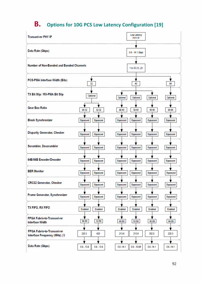
92
B. Options for 10G PCS Low Latency Configuration [19]
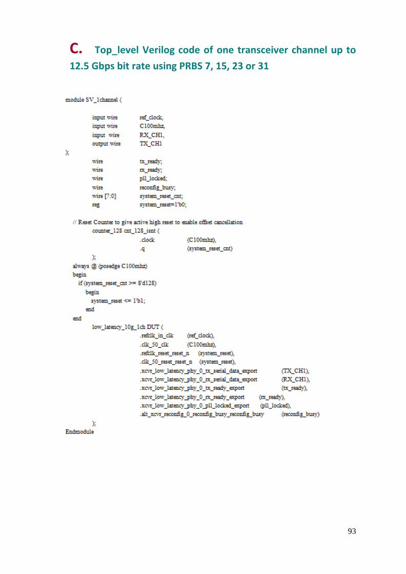
93
C. Top_level Verilog code of one transceiver channel up to
12.5 Gbps bit rate using PRBS 7, 15, 23 or 31

94
D. Block diagram of one transceiver channel up to 12.5 Gbps bit rate using PRBS 7, 15, 23 or 31
QSYS

95
E. Block diagram of seven transceiver channel transmitting at the same bit rate using PRBS 7, 15,
23 or 31
QSYS
96
F. Block diagram of seven transceiver channels transmitting at different bit rates up to 12.5 Gbps
using PRBS 7, 15, 23 or 31
QSYS_1
QSYS_2
QSYS_3

97
G. Top-level Verilog code of seven transceiver channels
transmitting at different bit rates up to 12.5 Gbps using
PRBS 7, 15, 23 or 31design

98

99
H. External Slave_Verilog code

100
I. Block diagram of one transceiver channel transmitting up 12.5 Gbps using fix data pattern
QSYS
Reconfiguration Controller
Pattern generator and checker
Low latency PHY core
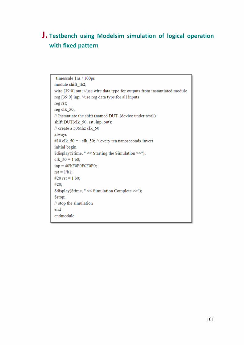
101
J. Testbench using Modelsim simulation of logical operation
with fixed pattern
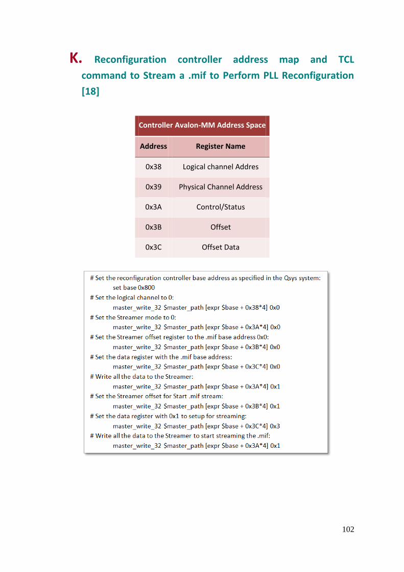
102
K. Reconfiguration controller address map and TCL
command to Stream a .mif to Perform PLL Reconfiguration
[18]
Controller Avalon-MM Address Space
Address Register Name
0x38 Logical channel Addres
0x39 Physical Channel Address
0x3A Control/Status
0x3B Offset
0x3C Offset Data

103
L. Qsys system of one transceiver channel with a long fix
pattern within an embedded RAM

104
M. External slave RAM. Verilog code

105
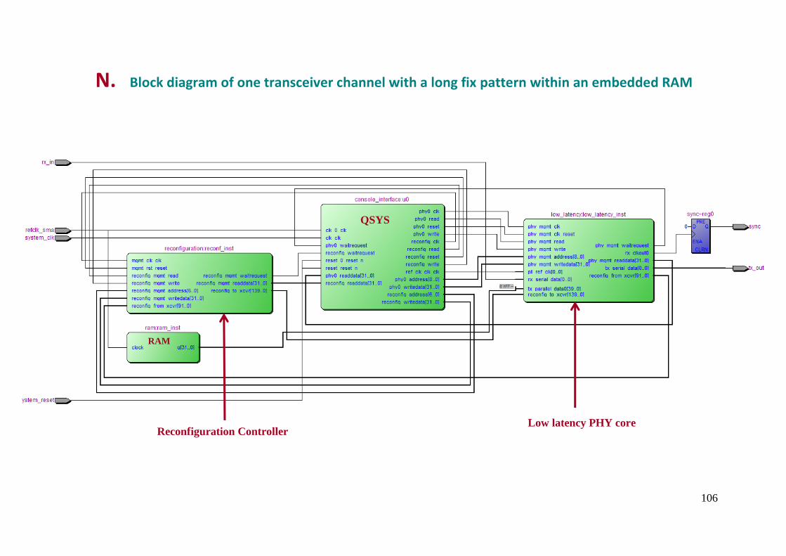
106
N. Block diagram of one transceiver channel with a long fix pattern within an embedded RAM
QSYS
RAM
Low latency PHY core Reconfiguration Controller