Flexible Electronics Production Deployment on FPD ... · •Advanced R&D findings can’t be...
14
Flexible Electronics Production Deployment on FPD Standards: Plastic Displays & Integrated Circuits Stanislav Loboda R&D engineer
Transcript of Flexible Electronics Production Deployment on FPD ... · •Advanced R&D findings can’t be...

Flexible Electronics Production Deployment on FPD Standards
Plastic Displays amp Integrated Circuits
Stanislav Loboda
RampD engineer
bull Gen 2 (370470 mm MG)bull 3600 sqm CR (incl 1700 sqm ISO5)bull Capacity ndash 10000 sqm TFT pabull Location ndashTroitsk Moscow area Russiabull Production ready ndash Q1 2019bull Invested by RUSNANO (Russian biggest
technology investment group)bull Managing by TechnoSpark (professional
venture-building company)
Plastic RFIDNFC-chip(02 scm)
Large-area backplane for sensors and displays (10 inch)
Organic Photo-detector (4 inch)
Flexible EPD (4 inch)
Products Technologies
IGZO TFTworldrsquos most powerful plastic ICs
Organic TFT enables truly flexible TFT arrays
The world-first small-volume contract manufacturingfor plastic TFT-arrays and ICs
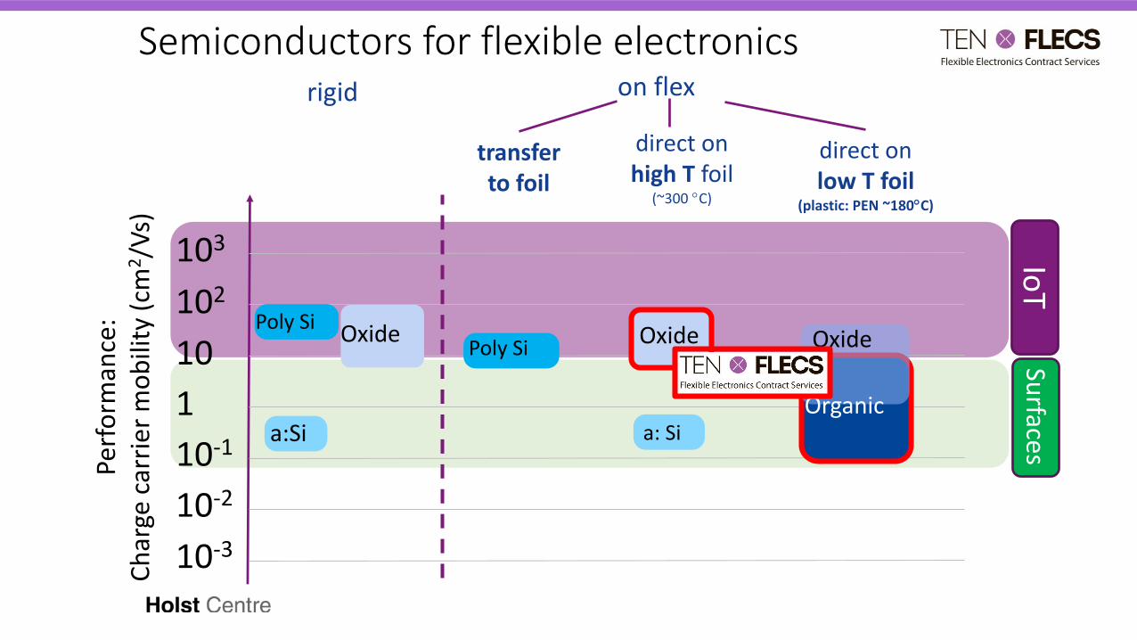
Semiconductors for flexible electronics
Perf
orm
ance
C
har
ge c
arri
er
mo
bili
ty (
cm2V
s)
10-3
10-2
10-1
1
10
102
103
aSi
Poly SiOxide
on flex
direct onlow T foil
(plastic PEN ~180C)
OxidePoly Si
transferto foil
direct onhigh T foil
(~300 C)
a SiOrganic
Oxide
IoT
Surface
srigid
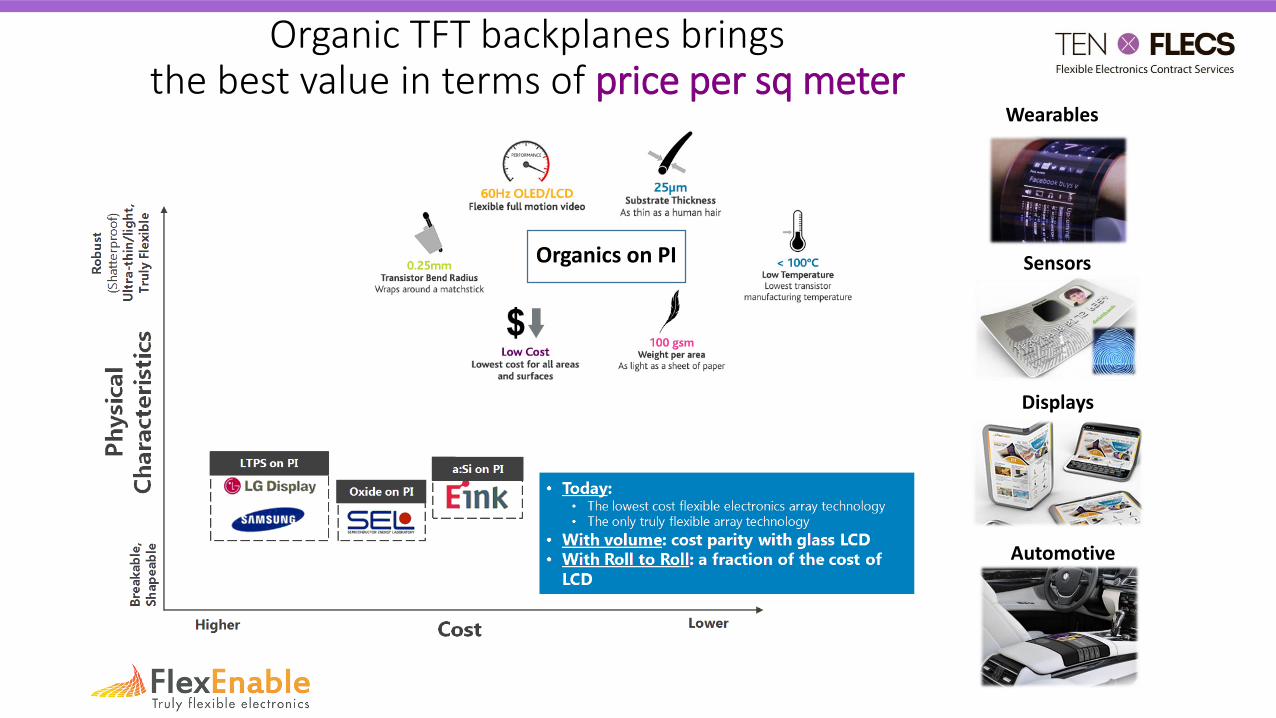
Organic TFT backplanes brings the best value in terms of price per sq meter
Automotive
Displays
Sensors
Wearables
Organics on PI
Wireless tagsRFID NFC
135MHz clock generators12-128bit code generatorsRectifiers modulators
Sensor interfacesADC (up to 6-bit)
Comps OpampsC2C-SARVCOIntegrated
MicroprocessorsX-bit core chipsALUsP2ROM integration
Signage control
7-segment driver ICPixel array driver IC
Standard cell libraries(building blocks in IGZO TFT)
eg AND OR XOR XNOR inverters
o Maximum performanceo Minimum power
o High Yield
MemoryLPROM P2ROM
Array architecturesRead-write controls
IGZO TFT ndash the best value in terms of price per function
IGZO TFT oTFT
Thickness lt20 microm flexible lightweight transparent low cost
Advantages high mobility productivity Advantages Truly flexible lowest cost
In future it is planned to combine organic and IGZO technologies in hybrid CMOS structures for number of applications such as logic circuits
Product
Prototype
RampD
Glass LCD-displays Plastic EPD-displays
LCD OLED DisplaysSensors X-RayampFingerprint
Light-emitting transistors for displays Roll-to-Roll printing
Temperature pressure X-ray image sensors
MicroprocessorMemoryNFC-tags
Logic
Applications of IGZO TFT and organic TFT
From wafers to panels ndash optimization of coating process
Source SID-2017 Reid Chesterfield et al
The non-round shape makes it hard to use all of
coated material off-rectangle material gets lost
Spin-coated material at peripheryis almost 25 thicker than slot-
coated and 3 times thicker comparing to the center point
Spin coated area
Slot coated area
G25
470
37
0
VSSpin coatingWidely used in Labs
Slit coatingIndustry applicable technology
Coating area perfectly fits rectangular glass less
material loss
Slot-die coating method yields more uniformity
ndash
ndash
+
+
Patterning techniques ndashphotolithography amp wetdry etching
View of mask frame optics path and substrate chuck
Scanner as an exposure tool provides accuracy of 3 μm which is enough for TEN FLECS OTFT design patterning
Wet etching
Throughput Less More
Cost More Less
Stepper Scanner
Accuracy More Less
Technologies of photolithography
Combination of resist coating exposure and developer working togetherSource Young Hee Byun et al IEEE 1996
Optical inspection is carried out across the entire mother glass active area to detect defects and to carry out CD-measurements
bull source-drain developbull source-drain etchbull gate developbull gate etchbull screen developbull screen etchbull top pixel developbull top pixel etch
Selective AOI provides more productivity vs individual No need for +1 tool
Optical inspection ndash critical dimension measurements
The effect of a large fibre that has caused problems for patterning the
gate layer and resulting in shorts
The defect caused problems for patterning the top pixel layer 15
pixels shorted together as a result
Automatic optical inspection (AOI) array test amp repair connected at one SPC to ensure maximum yield
Classification of defects
repairable not-repairable
Laser ablation by array repair tool
No further actions(utilized)
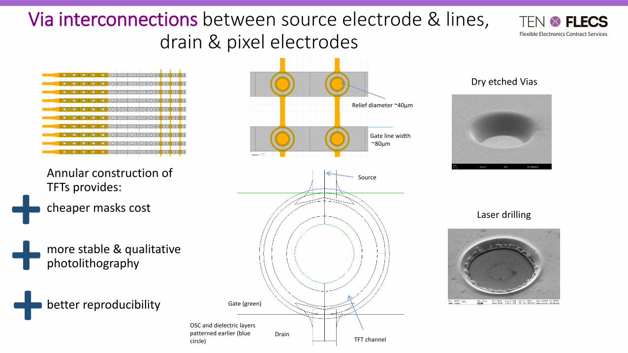
Annular construction of TFTs provides
cheaper masks cost
more stable amp qualitative photolithography
better reproducibility
Source
OSC and dielectric layers patterned earlier (blue circle)
Relief diameter ~40microm
Via interconnections between source electrode amp lines drain amp pixel electrodes
Gate (green)
Dry etched Vias
TFT channelDrain
Gate line width~80microm
++
Laser drilling
+
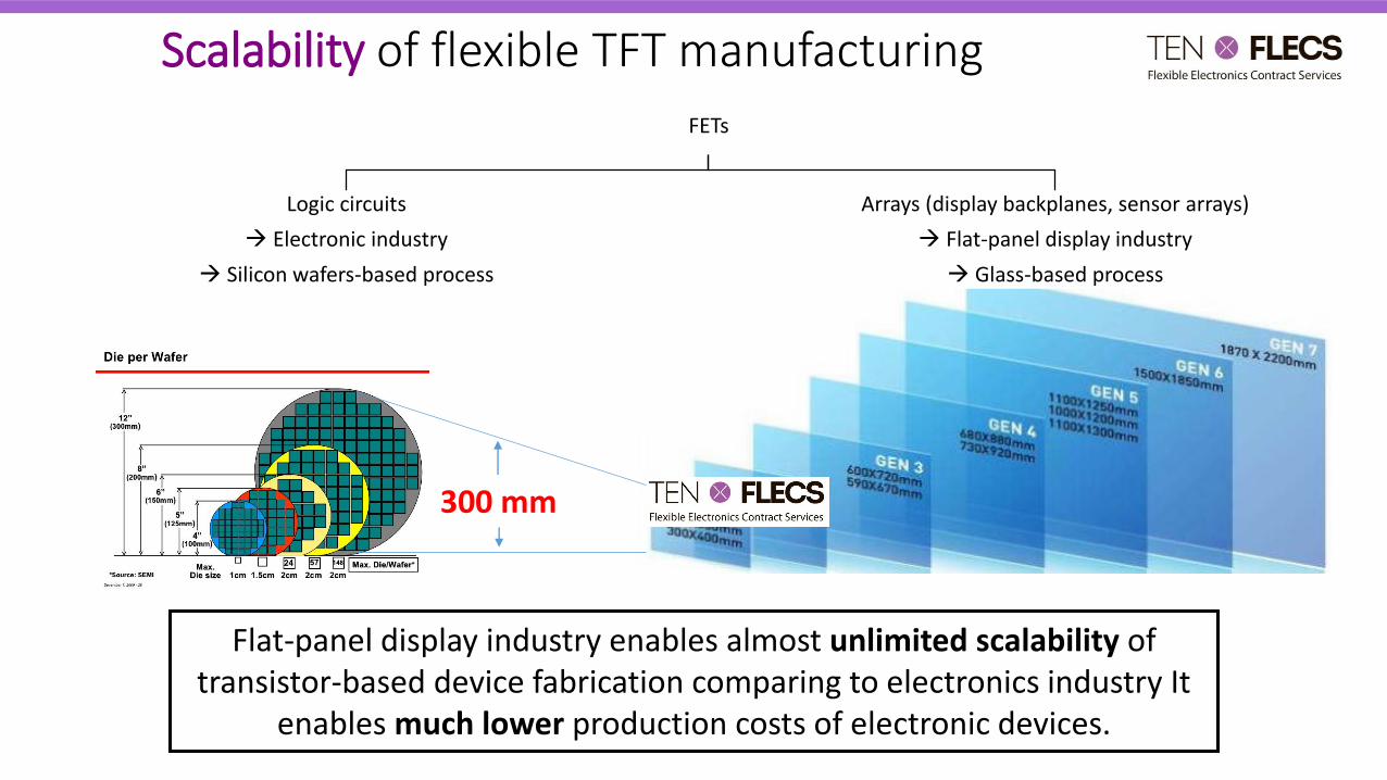
FETs
Logic circuits
Electronic industry
Silicon wafers-based process
Arrays (display backplanes sensor arrays)
Flat-panel display industry
Glass-based process
300 mm
Flat-panel display industry enables almost unlimited scalability of transistor-based device fabrication comparing to electronics industry It
enables much lower production costs of electronic devices
Scalability of flexible TFT manufacturing
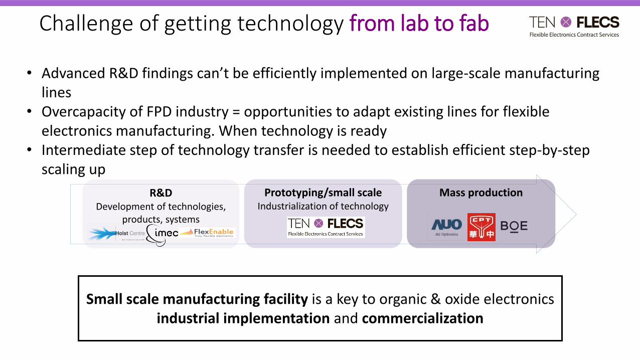
Small scale manufacturing facility is a key to organic amp oxide electronics industrial implementation and commercialization
Challenge of getting technology from lab to fab
Prototypingsmall scaleIndustrialization of technology
Mass productionRampDDevelopment of technologies
products systems
bull Advanced RampD findings canrsquot be efficiently implemented on large-scale manufacturing lines
bull Overcapacity of FPD industry = opportunities to adapt existing lines for flexible electronics manufacturing When technology is ready
bull Intermediate step of technology transfer is needed to establish efficient step-by-step scaling up
Conclusions
Industrial implementation stage of organic electronics
Organic TFT electronics together with IGZO TFT completes a platform for FPD manufacturing of flexible electronics
FPD process for TFT technology allows better scalability comparing to wafer process
Efficient scaling up of flexible electronics manufacturing process flow through small scale stage
14
Thank you
infotenflecscom
wwwtenflecscom

bull Gen 2 (370470 mm MG)bull 3600 sqm CR (incl 1700 sqm ISO5)bull Capacity ndash 10000 sqm TFT pabull Location ndashTroitsk Moscow area Russiabull Production ready ndash Q1 2019bull Invested by RUSNANO (Russian biggest
technology investment group)bull Managing by TechnoSpark (professional
venture-building company)
Plastic RFIDNFC-chip(02 scm)
Large-area backplane for sensors and displays (10 inch)
Organic Photo-detector (4 inch)
Flexible EPD (4 inch)
Products Technologies
IGZO TFTworldrsquos most powerful plastic ICs
Organic TFT enables truly flexible TFT arrays
The world-first small-volume contract manufacturingfor plastic TFT-arrays and ICs
Semiconductors for flexible electronics
Perf
orm
ance
C
har
ge c
arri
er
mo
bili
ty (
cm2V
s)
10-3
10-2
10-1
1
10
102
103
aSi
Poly SiOxide
on flex
direct onlow T foil
(plastic PEN ~180C)
OxidePoly Si
transferto foil
direct onhigh T foil
(~300 C)
a SiOrganic
Oxide
IoT
Surface
srigid
Organic TFT backplanes brings the best value in terms of price per sq meter
Automotive
Displays
Sensors
Wearables
Organics on PI
Wireless tagsRFID NFC
135MHz clock generators12-128bit code generatorsRectifiers modulators
Sensor interfacesADC (up to 6-bit)
Comps OpampsC2C-SARVCOIntegrated
MicroprocessorsX-bit core chipsALUsP2ROM integration
Signage control
7-segment driver ICPixel array driver IC
Standard cell libraries(building blocks in IGZO TFT)
eg AND OR XOR XNOR inverters
o Maximum performanceo Minimum power
o High Yield
MemoryLPROM P2ROM
Array architecturesRead-write controls
IGZO TFT ndash the best value in terms of price per function
IGZO TFT oTFT
Thickness lt20 microm flexible lightweight transparent low cost
Advantages high mobility productivity Advantages Truly flexible lowest cost
In future it is planned to combine organic and IGZO technologies in hybrid CMOS structures for number of applications such as logic circuits
Product
Prototype
RampD
Glass LCD-displays Plastic EPD-displays
LCD OLED DisplaysSensors X-RayampFingerprint
Light-emitting transistors for displays Roll-to-Roll printing
Temperature pressure X-ray image sensors
MicroprocessorMemoryNFC-tags
Logic
Applications of IGZO TFT and organic TFT
From wafers to panels ndash optimization of coating process
Source SID-2017 Reid Chesterfield et al
The non-round shape makes it hard to use all of
coated material off-rectangle material gets lost
Spin-coated material at peripheryis almost 25 thicker than slot-
coated and 3 times thicker comparing to the center point
Spin coated area
Slot coated area
G25
470
37
0
VSSpin coatingWidely used in Labs
Slit coatingIndustry applicable technology
Coating area perfectly fits rectangular glass less
material loss
Slot-die coating method yields more uniformity
ndash
ndash
+
+
Patterning techniques ndashphotolithography amp wetdry etching
View of mask frame optics path and substrate chuck
Scanner as an exposure tool provides accuracy of 3 μm which is enough for TEN FLECS OTFT design patterning
Wet etching
Throughput Less More
Cost More Less
Stepper Scanner
Accuracy More Less
Technologies of photolithography
Combination of resist coating exposure and developer working togetherSource Young Hee Byun et al IEEE 1996
Optical inspection is carried out across the entire mother glass active area to detect defects and to carry out CD-measurements
bull source-drain developbull source-drain etchbull gate developbull gate etchbull screen developbull screen etchbull top pixel developbull top pixel etch
Selective AOI provides more productivity vs individual No need for +1 tool
Optical inspection ndash critical dimension measurements
The effect of a large fibre that has caused problems for patterning the
gate layer and resulting in shorts
The defect caused problems for patterning the top pixel layer 15
pixels shorted together as a result
Automatic optical inspection (AOI) array test amp repair connected at one SPC to ensure maximum yield
Classification of defects
repairable not-repairable
Laser ablation by array repair tool
No further actions(utilized)
Annular construction of TFTs provides
cheaper masks cost
more stable amp qualitative photolithography
better reproducibility
Source
OSC and dielectric layers patterned earlier (blue circle)
Relief diameter ~40microm
Via interconnections between source electrode amp lines drain amp pixel electrodes
Gate (green)
Dry etched Vias
TFT channelDrain
Gate line width~80microm
++
Laser drilling
+
FETs
Logic circuits
Electronic industry
Silicon wafers-based process
Arrays (display backplanes sensor arrays)
Flat-panel display industry
Glass-based process
300 mm
Flat-panel display industry enables almost unlimited scalability of transistor-based device fabrication comparing to electronics industry It
enables much lower production costs of electronic devices
Scalability of flexible TFT manufacturing
Small scale manufacturing facility is a key to organic amp oxide electronics industrial implementation and commercialization
Challenge of getting technology from lab to fab
Prototypingsmall scaleIndustrialization of technology
Mass productionRampDDevelopment of technologies
products systems
bull Advanced RampD findings canrsquot be efficiently implemented on large-scale manufacturing lines
bull Overcapacity of FPD industry = opportunities to adapt existing lines for flexible electronics manufacturing When technology is ready
bull Intermediate step of technology transfer is needed to establish efficient step-by-step scaling up
Conclusions
Industrial implementation stage of organic electronics
Organic TFT electronics together with IGZO TFT completes a platform for FPD manufacturing of flexible electronics
FPD process for TFT technology allows better scalability comparing to wafer process
Efficient scaling up of flexible electronics manufacturing process flow through small scale stage
14
Thank you
infotenflecscom
wwwtenflecscom

14
Thank you
infotenflecscom
wwwtenflecscom