Flexible and Printed Electronics for Displays and Image ... · PDF filePARC Overview •...
37
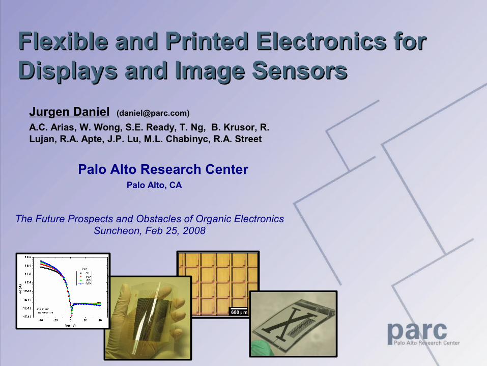
680 μ m Flexible and Printed Electronics for Flexible and Printed Electronics for Displays and Image Sensors Displays and Image Sensors Jurgen Daniel ([email protected]) A.C. Arias, W. Wong, S.E. Ready, T. Ng, B. Krusor, R. Lujan, R.A. Apte, J.P. Lu, M.L. Chabinyc, R.A. Street Palo Alto Research Center Palo Alto, CA The Future Prospects and Obstacles of Organic Electronics Suncheon, Feb 25, 2008
Transcript of Flexible and Printed Electronics for Displays and Image ... · PDF filePARC Overview •...
680 µ m
Flexible and Printed Electronics for Flexible and Printed Electronics for Displays and Image SensorsDisplays and Image Sensors
Jurgen Daniel ([email protected])
A.C. Arias, W. Wong, S.E. Ready, T. Ng, B. Krusor, R. Lujan, R.A. Apte, J.P. Lu, M.L. Chabinyc, R.A. Street
Palo Alto Research CenterPalo Alto, CA
The Future Prospects and Obstacles of Organic ElectronicsSuncheon, Feb 25, 2008
OutlineOutline
A few words about PARC Motivation for flexible and printed electronics Required components for printed electronics
– Printer– Materials– TFT performance
Display and sensor applications Some of the challenges for printed pixel circuits
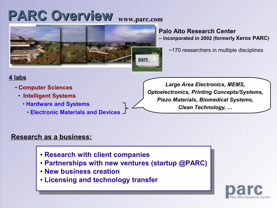
PARC OverviewPARC Overview
• Electronic Materials and Devices• Hardware and Systems
• Computer Sciences• Intelligent Systems
Palo Alto Research Center – incorporated in 2002 (formerly Xerox PARC)
~170 researchers in multiple disciplines
4 labs
www.parc.com
Large Area Electronics, MEMS, Optoelectronics, Printing Concepts/Systems,
Piezo Materials, Biomedical Systems,Clean Technology, ...
• Research with client companies• Partnerships with new ventures (startup @PARC) • New business creation • Licensing and technology transfer
Research as a business:

Large-Area Electronics at PARCLarge-Area Electronics at PARC
Low temperature a-Si on plastic
X-ray imagers
LTPS OLED backplane on steel
Jet-printed digital lithography of a-Si TFTs
displays
Technologies Amorphous silicon (a-Si) Low-temperature amorphous Si Low-temperature poly Si (LTPS) Organic semiconductor processes Jet-printed electronics
PARC R&D services:• Prototyping and System design• Testing and Characterization
(W. Wong, et al.)
(J.P. Lu, et al.)

Large-Area Electronics at PARCLarge-Area Electronics at PARC
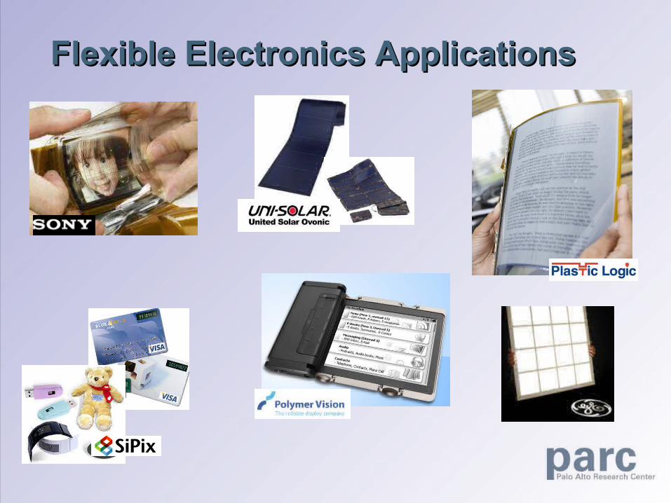
Flexible Electronics ApplicationsFlexible Electronics Applications
Motivation for Printed ElectronicsMotivation for Printed Electronics
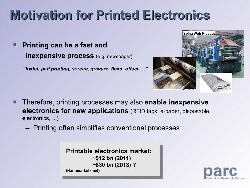
Printing can be a fast and inexpensive process (e.g. newspaper)
Therefore, printing processes may also enable inexpensive electronics for new applications (RFID tags, e-paper, disposable electronics, ...)
– Printing often simplifies conventional processes
Solna Web Presses
“inkjet, pad printing, screen, gravure, flexo, offset, ...”
Printable electronics market: ~$12 bn (2011) ~$30 bn (2013) ?
(Nanomarkets.net)
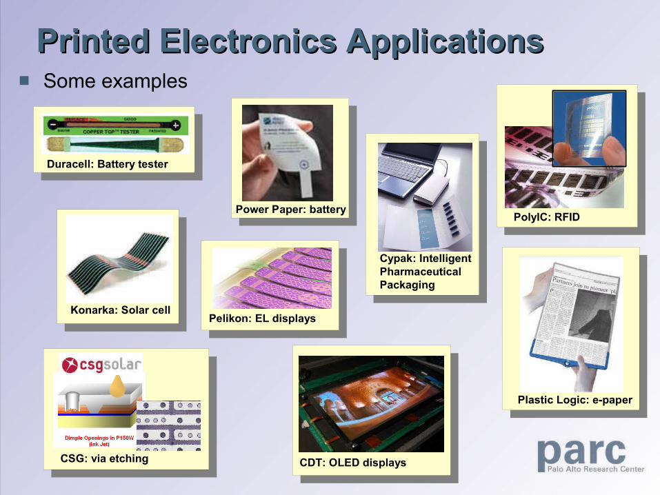
Printed Electronics ApplicationsPrinted Electronics Applications
Duracell: Battery tester
Cypak: Intelligent Pharmaceutical Packaging
PolyIC: RFID
CSG: via etching
Plastic Logic: e-paper
CDT: OLED displays
Konarka: Solar cellPelikon: EL displays
Some examples
Power Paper: battery
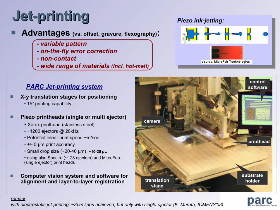
Jet-printing Jet-printing
X-y translation stages for positioning• 15” printing capability
Piezo printheads (single or multi ejector)• Xerox printhead (stainless steel)• ~1200 ejectors @ 20kHz• Potential linear print speed ~m/sec• +/- 5 µm print accuracy• Small drop size (~20-40 µm)• using also Spectra (~128 ejectors) and MicroFab (single ejector) print heads
Computer vision system and software for alignment and layer-to-layer registration
~10-20 pL
remark:with electrostatic jet-printing: ~3µm lines achieved, but only with single ejector (K. Murata, ICMENS'03)
PARC Jet-printing system
camera
printhead
control software
substrate holdertranslation
stage
Piezo ink-jetting:
Advantages (vs. offset, gravure, flexography):- variable pattern- on-the-fly error correction- non-contact- wide range of materials (incl. hot-melt)
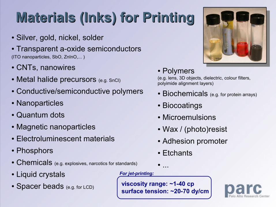
Materials (Inks) for PrintingMaterials (Inks) for Printing
(ITO nanoparticles, SbO, ZnInO,... )
● Polymers (e.g. lens, 3D objects, dielectric, colour filters,polyimide alignment layers)
● Phosphors
● Biocoatings
● Etchants
● Silver, gold, nickel, solder
● Magnetic nanoparticles
● Quantum dots
● Metal halide precursors (e.g. SnCl)
● Transparent a-oxide semiconductors
● Electroluminescent materials
● CNTs, nanowires
● Microemulsions
● Liquid crystals● Spacer beads (e.g. for LCD)
● Chemicals (e.g. explosives, narcotics for standards)
● Biochemicals (e.g. for protein arrays)● Conductive/semiconductive polymers● Nanoparticles
● Adhesion promoter
● Wax / (photo)resist
● ...
viscosity range: ~1-40 cpsurface tension: ~20-70 dy/cm
For jet-printing:
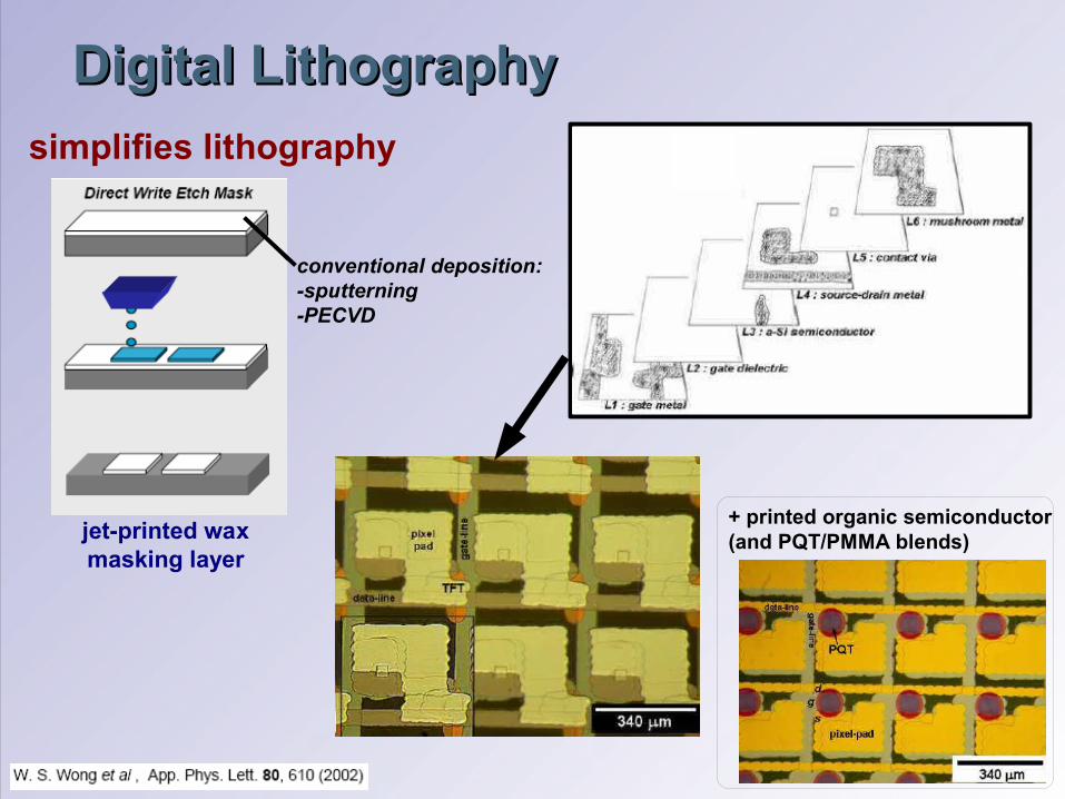
Digital LithographyDigital Lithographysimplifies lithography
+ printed organic semiconductor(and PQT/PMMA blends)jet-printed wax
masking layer
conventional deposition:-sputterning-PECVD
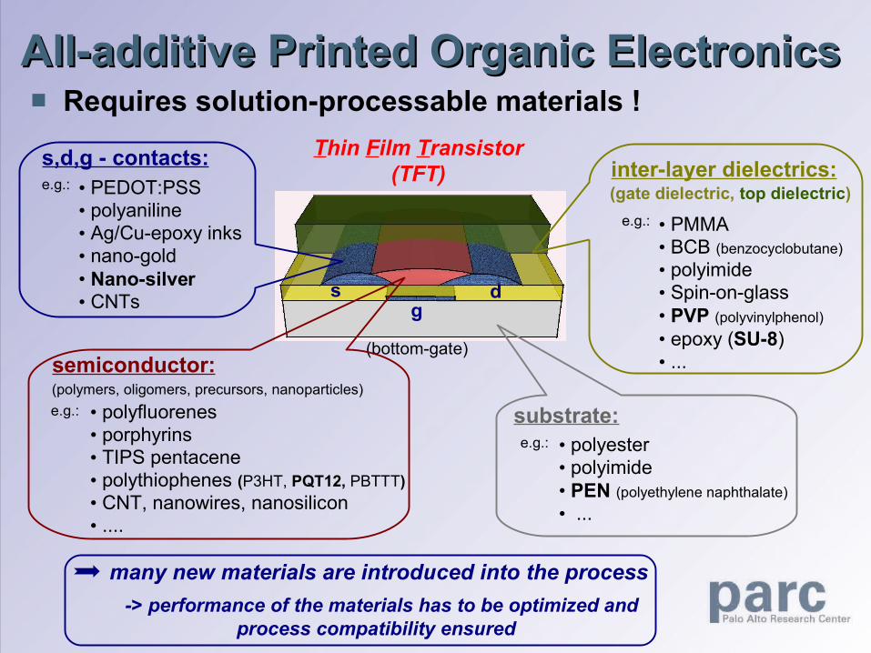
All-additive Printed Organic ElectronicsAll-additive Printed Organic Electronics
s,d,g - contacts:• PEDOT:PSS• polyaniline• Ag/Cu-epoxy inks• nano-gold• Nano-silver• CNTs
Thin Film Transistor(TFT)
(bottom-gate)semiconductor:(polymers, oligomers, precursors, nanoparticles)
• polyfluorenes• porphyrins • TIPS pentacene• polythiophenes (P3HT, PQT12, PBTTT)• CNT, nanowires, nanosilicon • ....
e.g.:
e.g.:
substrate:• polyester• polyimide• PEN (polyethylene naphthalate)• ...
e.g.:
gds
inter-layer dielectrics:
• PMMA • BCB (benzocyclobutane)• polyimide• Spin-on-glass • PVP (polyvinylphenol)• epoxy (SU-8)• ...
e.g.:
(gate dielectric, top dielectric)
many new materials are introduced into the process -> performance of the materials has to be optimized and
process compatibility ensured
Requires solution-processable materials !
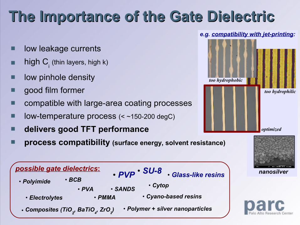
The Importance of the Gate Dielectric The Importance of the Gate Dielectric
too hydrophobic
too hydrophilic
e.g. compatibility with jet-printing:
• Composites (TiO2, BaTiO
4, ZrO
2) • Polymer + silver nanoparticles
• Cyano-based resins• Electrolytes
• Polyimide
possible gate dielectrics:
• SANDS• BCB
• PVA
• PVP • SU-8 • Glass-like resins
• PMMA
• Cytop
optimized
low leakage currents high C
i (thin layers, high k)
low pinhole density good film former compatible with large-area coating processes low-temperature process (< ~150-200 degC)
delivers good TFT performance process compatibility (surface energy, solvent resistance)
nanosilver
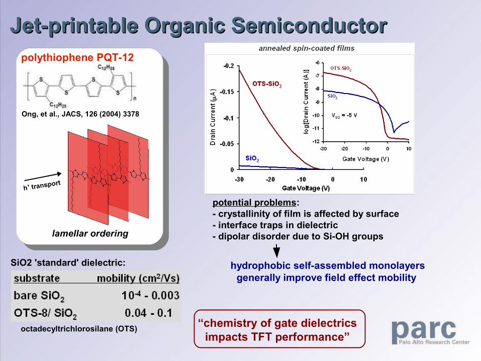
Jet-printable Organic Semiconductor Jet-printable Organic Semiconductor
hydrophobic self-assembled monolayers generally improve field effect mobility
“chemistry of gate dielectrics impacts TFT performance”
octadecyltrichlorosilane (OTS)
lamellar ordering
Ong, et al., JACS, 126 (2004) 3378
polythiophene PQT-12
potential problems:- crystallinity of film is affected by surface- interface traps in dielectric- dipolar disorder due to Si-OH groups
h+ transport
SiO2 'standard' dielectric:
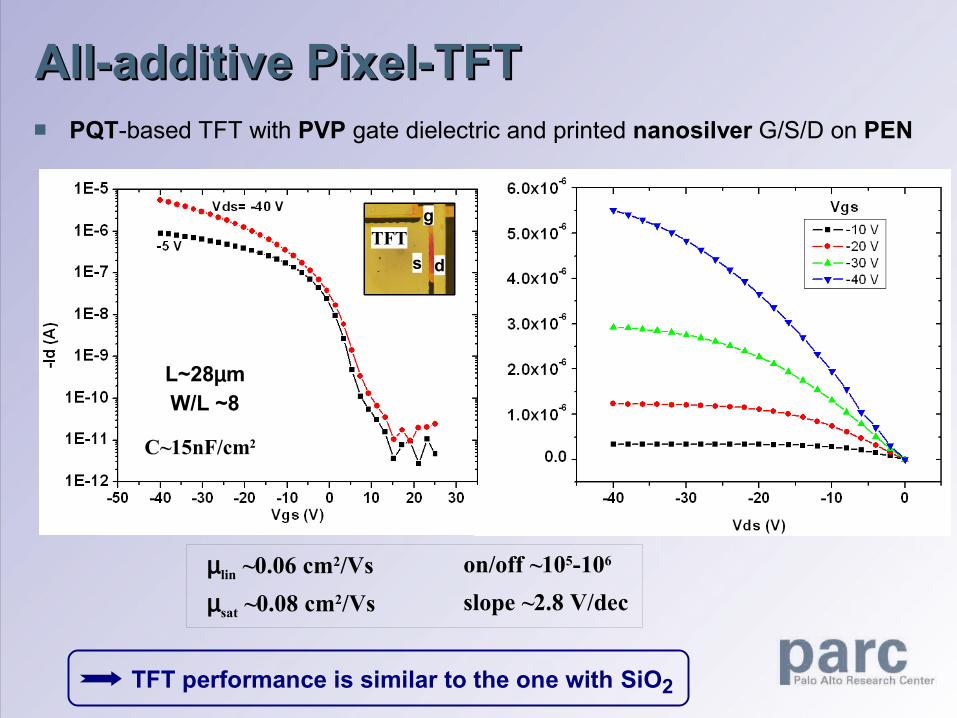
All-additive Pixel-TFT All-additive Pixel-TFT PQT-based TFT with PVP gate dielectric and printed nanosilver G/S/D on PEN
L~28µmW/L ~8
C~15nF/cm2
on/off ~105-106
slope ~2.8 V/decµlin ~0.06 cm2/Vsµsat ~0.08 cm2/Vs
TFT performance is similar to the one with SiO2
TFTs d
g
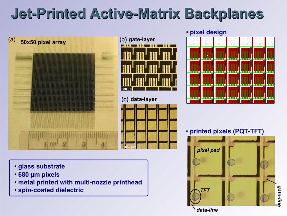
Jet-Printed Active-Matrix BackplanesJet-Printed Active-Matrix Backplanes (a) (b)
(c)
680 µ m
680 µ m
(a) (b)
(c)
680 µ m
680 µ m
50x50 pixel array
• glass substrate • 680 µm pixels• metal printed with multi-nozzle printhead• spin-coated dielectric
gate-layer
data-layer
• pixel design
• printed pixels (PQT-TFT)
pixel pad
TFT
data-line
gate-line
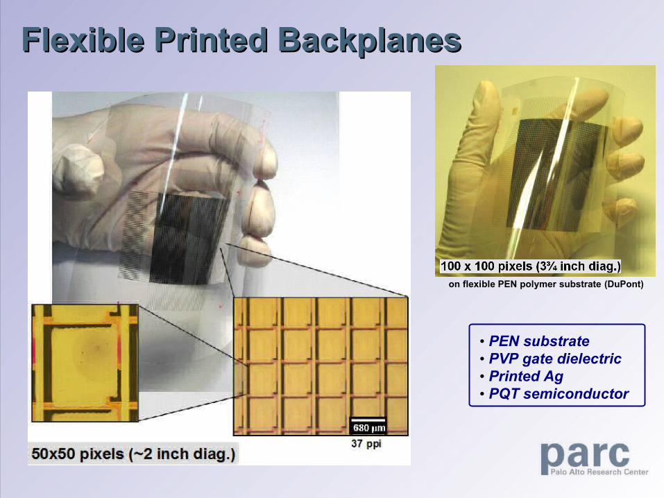
Flexible Printed BackplanesFlexible Printed Backplanes
on flexible PEN polymer substrate (DuPont)
• PEN substrate• PVP gate dielectric• Printed Ag• PQT semiconductor
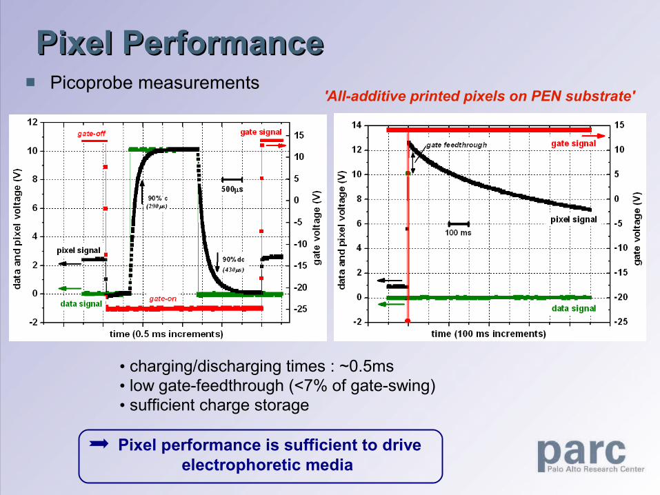
Pixel PerformancePixel Performance'All-additive printed pixels on PEN substrate'
• charging/discharging times : ~0.5ms• low gate-feedthrough (<7% of gate-swing)• sufficient charge storage
Pixel performance is sufficient to drive electrophoretic media
Picoprobe measurements
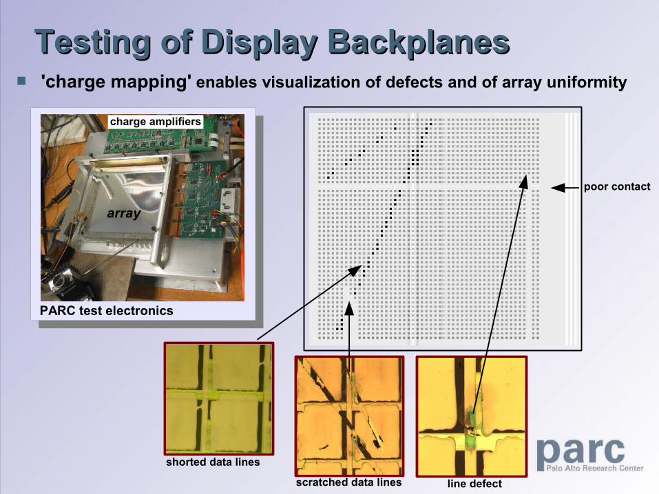
Testing of Display Backplanes Testing of Display Backplanes
poor contact
scratched data lines
shorted data lines
line defect
PARC test electronics
array
charge amplifiers
'charge mapping' enables visualization of defects and of array uniformity
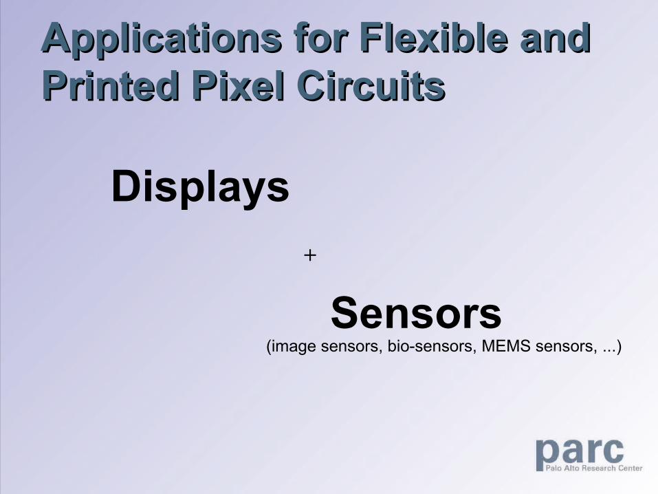
Applications for Flexible and Applications for Flexible and Printed Pixel CircuitsPrinted Pixel Circuits
Displays
Sensors+
(image sensors, bio-sensors, MEMS sensors, ...)
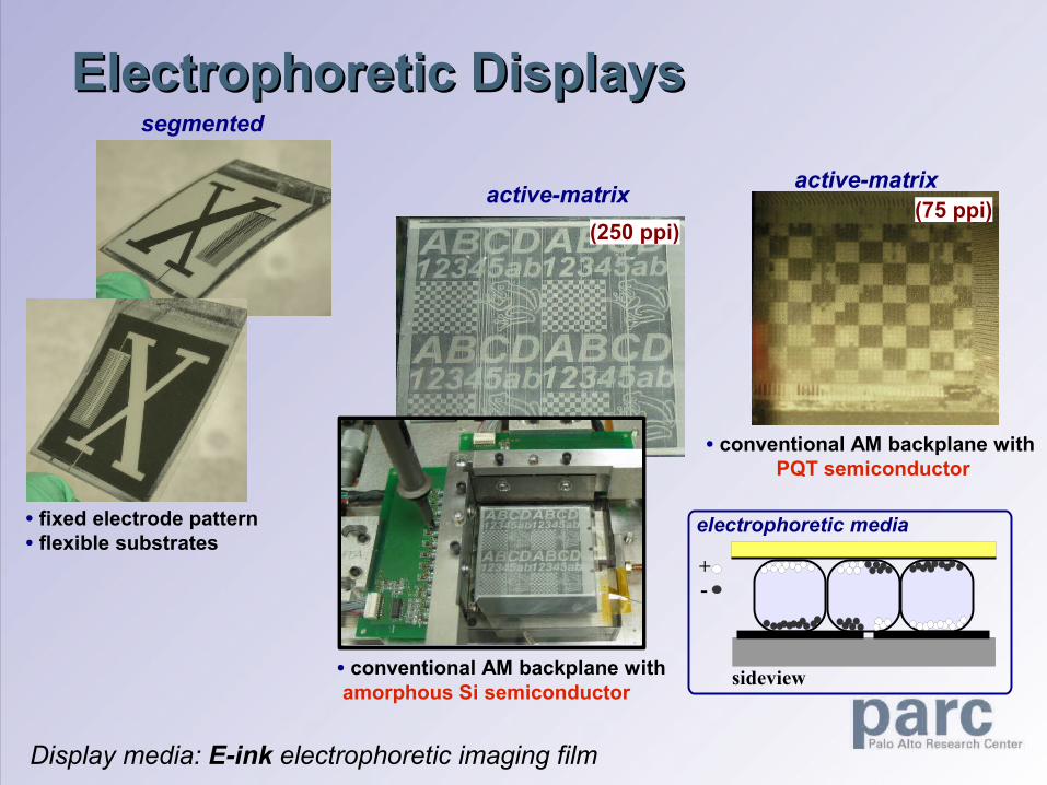
Electrophoretic DisplaysElectrophoretic Displays
● conventional AM backplane with PQT semiconductor
● fixed electrode pattern● flexible substrates
● conventional AM backplane with amorphous Si semiconductor
Display media: E-ink electrophoretic imaging film
active-matrix active-matrix
segmented
(250 ppi)(75 ppi)
+-
sideview
electrophoretic media

Flex Displays with Low-T a-SiFlex Displays with Low-T a-Si
6” flexible display (E-ink media)
bistable image after ~1 month
• 6” digital lithography array
• 8” photolithography array on PEN
(printed mask layers)
TFT:
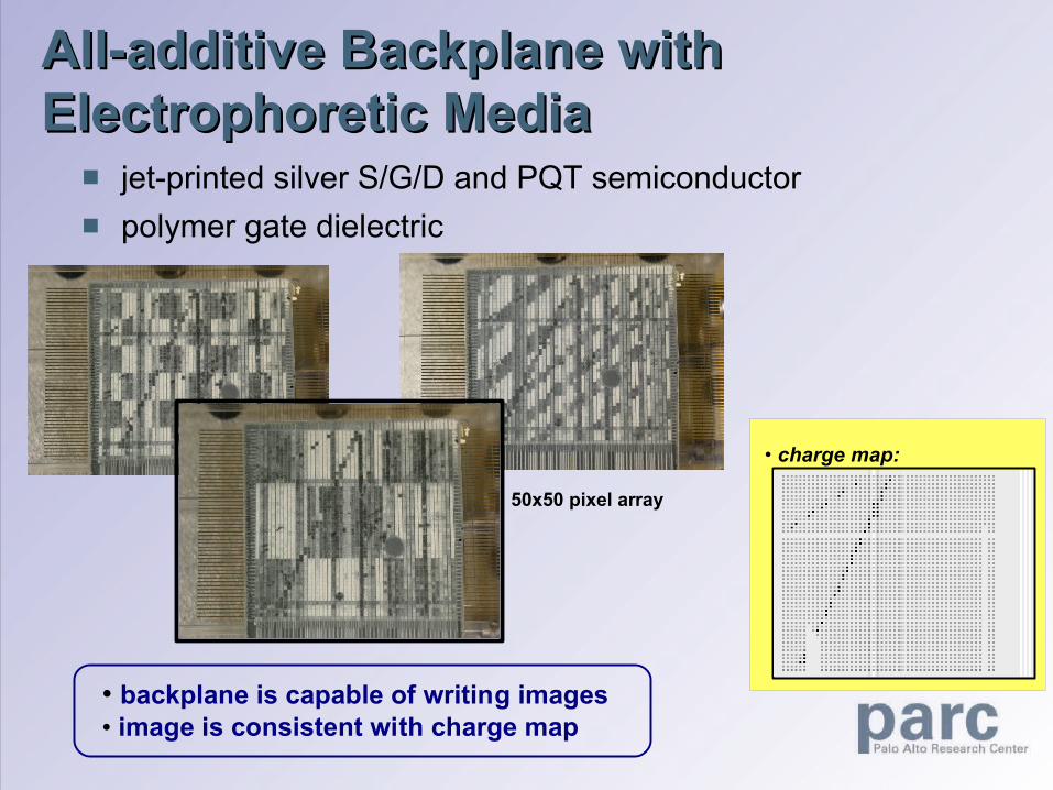
All-additive Backplane with All-additive Backplane with Electrophoretic MediaElectrophoretic Media
jet-printed silver S/G/D and PQT semiconductor polymer gate dielectric
• charge map:
• backplane is capable of writing images• image is consistent with charge map
50x50 pixel array

Sensor Applications Sensor Applications
X-ray imageX-ray image
B/W light imageB/W light image
• 180x180 pixel, 75dpi array• low-T a-Si:H TFTs and p-i-n sensors• flexible PEN substrate • reduced film stress
170 degC process on PEN (photolithography)
p-i-n images sensor arrays on flexible substrate
digital lithography + we are also exploring organic photo sensor materials

LTPS on Flexible Stainless SteelLTPS on Flexible Stainless Steel• LTPS: Laser recrystallized a-Si
PMOS mobilities up to 59 cm2/Vs
• QVGA full color OLED display demonstrated (collaboration with UDC and L3)
• TFT performance similar to TFTs on glass
UDC'sphosphorescent
OLED
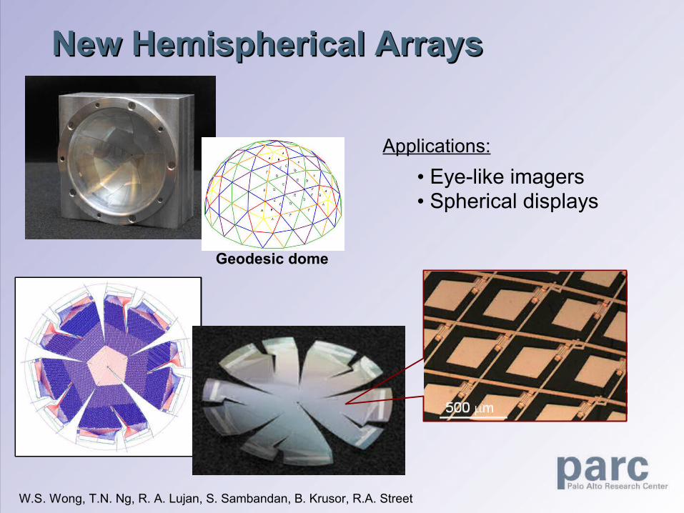
New Hemispherical ArraysNew Hemispherical Arrays
Geodesic dome
• Eye-like imagers• Spherical displays
W.S. Wong, T.N. Ng, R. A. Lujan, S. Sambandan, B. Krusor, R.A. Street
Applications:

Challenges for Printed BackplanesChallenges for Printed Backplanes
Higher display resolution
Device stability (environmental, Vt shift)
Circuit speed (e.g. for full video or for printed driver circuitry)
Cost of driver electronics and battery, versus printed backplane (transferred ICs, printed batteries ?)
Printing yield
Large-scale manufacturing (Roll-to Roll)

Challenge: Higher ResolutionChallenge: Higher Resolution
a) b) c)340 µ m680 µ m 170 µ m
a.r. ~72% a.r. ~58% a.r. ~32%
decreasing aperture ratio
• improve printing process (line width / spaces)• multi-layer pixel design
Higher display resolution requires smaller pixels
increasing pixel count
solutions

Improved Printing Process Improved Printing Process Printing of narrow lines Printing of narrow spaces
10 µm
• short TFT channel length• increased pixel aperture ratio
minimum value is determined by drop placement accuracy
53 µm
printed nano-silver
decreasing surface energy
~53 µm
57 µm
minimum value depends on surfaces and printhead
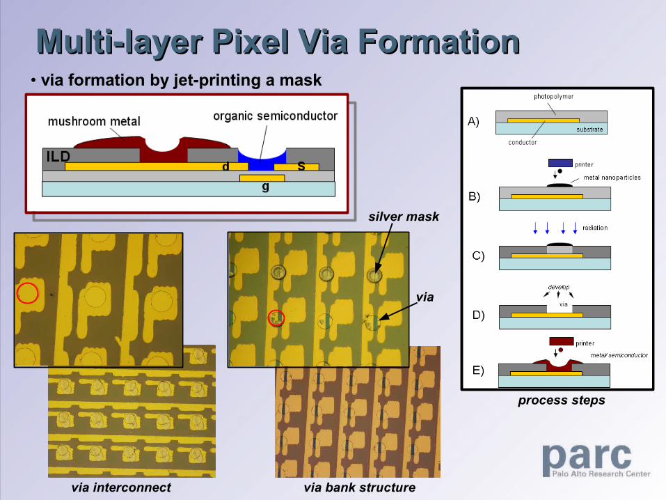
Multi-layer Pixel Via Formation Multi-layer Pixel Via Formation
• via formation by jet-printing a mask
process steps
silver mask
via interconnect via bank structure
via

Multi-layer Pixel with Molded DielectricMulti-layer Pixel with Molded Dielectric(for higher resolution)(for higher resolution)
• side view
• top view
Multi-layer pixel
printed wax pillar
~30 µm
polymer dielectric
Ag interconnect
• metal interconnect in molded UV polymer
• sacrificial wax pillarvias in molded UV polymer
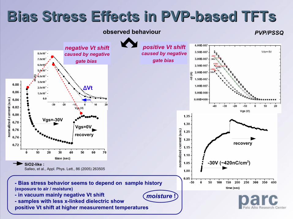
Bias Stress Effects in PVP-based TFTs Bias Stress Effects in PVP-based TFTs PVP/PSSQ
SiO2-like :Salleo, et al., Appl. Phys. Lett., 86 (2005) 263505
- Bias stress behavior seems to depend on sample history (exposure to air / moisture)- in vacuum mainly negative Vt shift- samples with less x-linked dielectric show positive Vt shift at higher measurement temperatures
Vgs=0VVgs=-30V
recovery
-30V (~420nC/cm2)
recovery
∆Vt
observed behaviour
negative Vt shiftcaused by negative
gate bias
positive Vt shiftcaused by negative
gate bias
moisture !
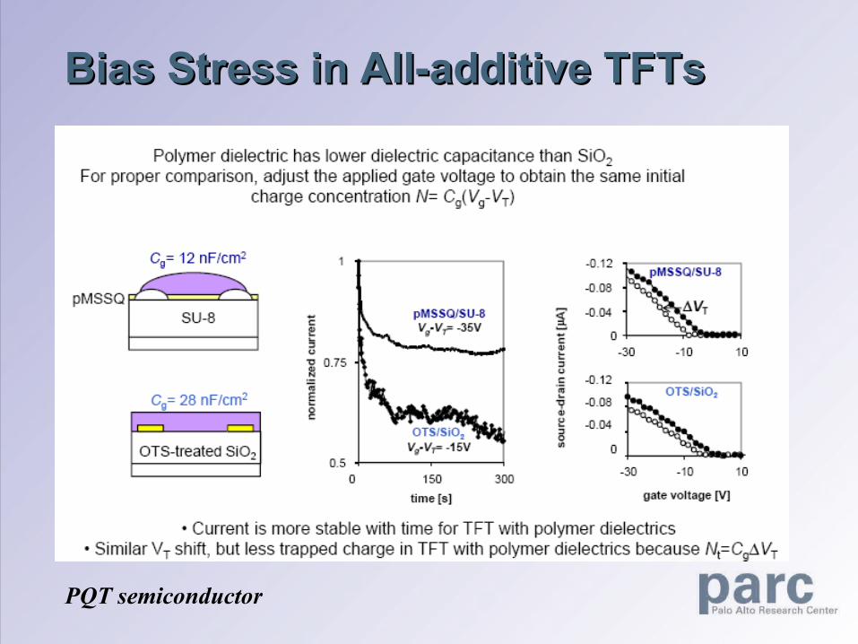
Bias Stress in All-additive TFTsBias Stress in All-additive TFTs
PQT semiconductor
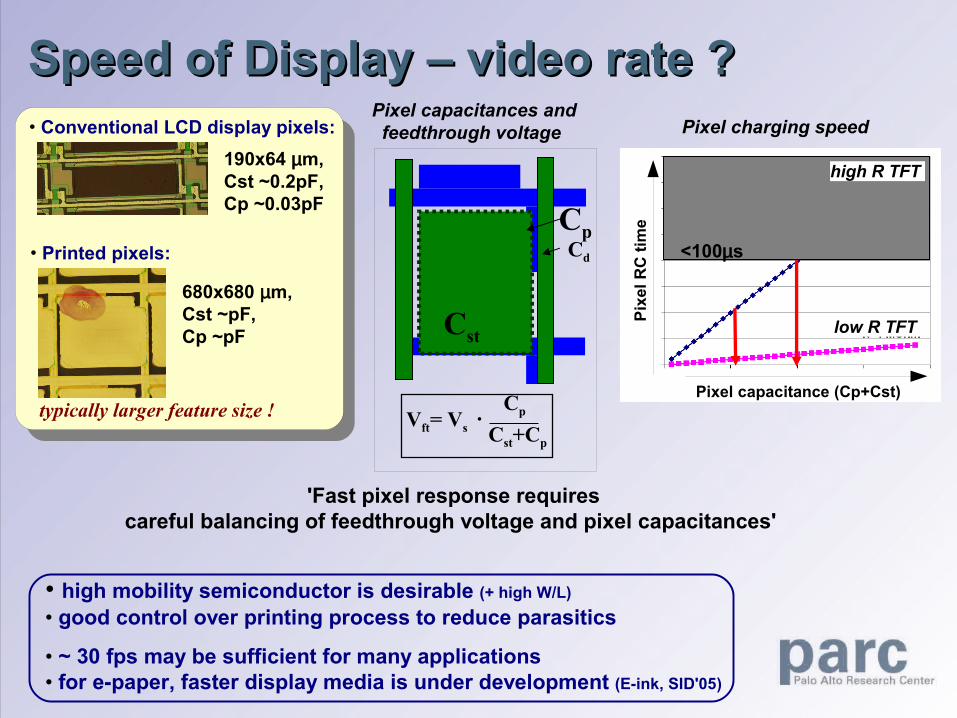
Speed of Display – video rate ?Speed of Display – video rate ?
190x64 µm, Cst ~0.2pF, Cp ~0.03pF
680x680 µm, Cst ~pF, Cp ~pF Cst
CpCd
Vft= Vs
Cp
Cst+Cp
·
• high mobility semiconductor is desirable (+ high W/L)• good control over printing process to reduce parasitics
• ~ 30 fps may be sufficient for many applications• for e-paper, faster display media is under development (E-ink, SID'05)
• Conventional LCD display pixels:
• Printed pixels:
'Fast pixel response requires careful balancing of feedthrough voltage and pixel capacitances'
Pixel capacitances and feedthrough voltage
Pixel capacitance (Cp+Cst)
Pixe
l RC
tim
e
<100µs
high R TFT
low R TFT
Pixel charging speed
typically larger feature size !
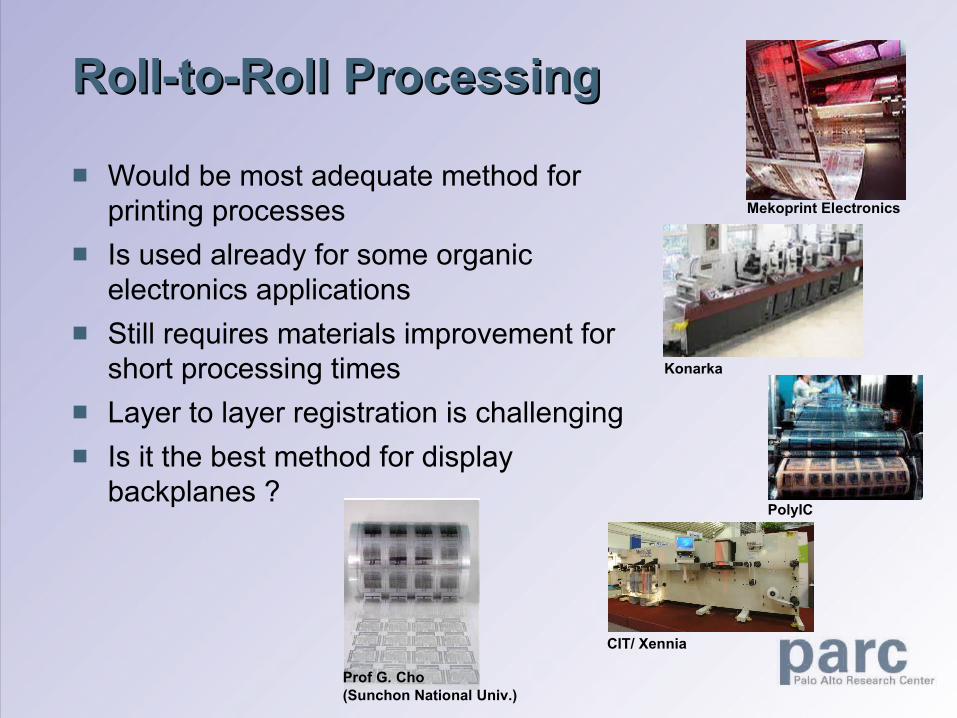
Roll-to-Roll ProcessingRoll-to-Roll Processing
Mekoprint Electronics
Konarka
PolyIC
CIT/ Xennia
Would be most adequate method for printing processes
Is used already for some organic electronics applications
Still requires materials improvement for short processing times
Layer to layer registration is challenging Is it the best method for display
backplanes ?
Prof G. Cho(Sunchon National Univ.)
Summary and OutlookSummary and Outlook PARC has a wide portfolio of flexible backplane
technologies All-additive printed electronics promises ultimate cost
savings Many new materials are introduced in the process -
performance/lifetime of the materials has to be investigated
Low resolution pixel circuits e.g. for signage-type applications
Higher resolution -> multilayer pixel design or narrower printed lines
Prototype electrophoretic displays have been fabricated

AcknowledgmentAcknowledgment
PARC: processing line underJackson Ho
Xerox Research Centre of Canada: Ping Liu, Yiliang Wu
NIST: partial funding
Dupont Teijin: PEN substrates
E-Ink: collaboration on electrophoretic media