Flex Design Guide
7
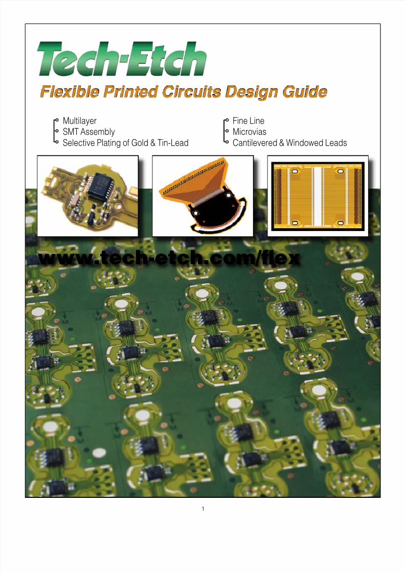
1 Fine Line Microvias Cantilevered & Windowed Leads Flexible Printed Circuits Design Guide Multilayer SMT Assembly Selective Plating of Gold & Tin-Lead www.tech-etch.com/flex
Transcript of Flex Design Guide
8/12/2019 Flex Design Guide
http://slidepdf.com/reader/full/flex-design-guide 1/61
Fine LineMicrovias
Cantilevered & Windowed Leads
Flexible Printed Circuits Design Guide MultilayerSMT Assembly
Selective Plating of Gold & Tin-Lead
www.tech-etch.com/flex
8/12/2019 Flex Design Guide
http://slidepdf.com/reader/full/flex-design-guide 2/6
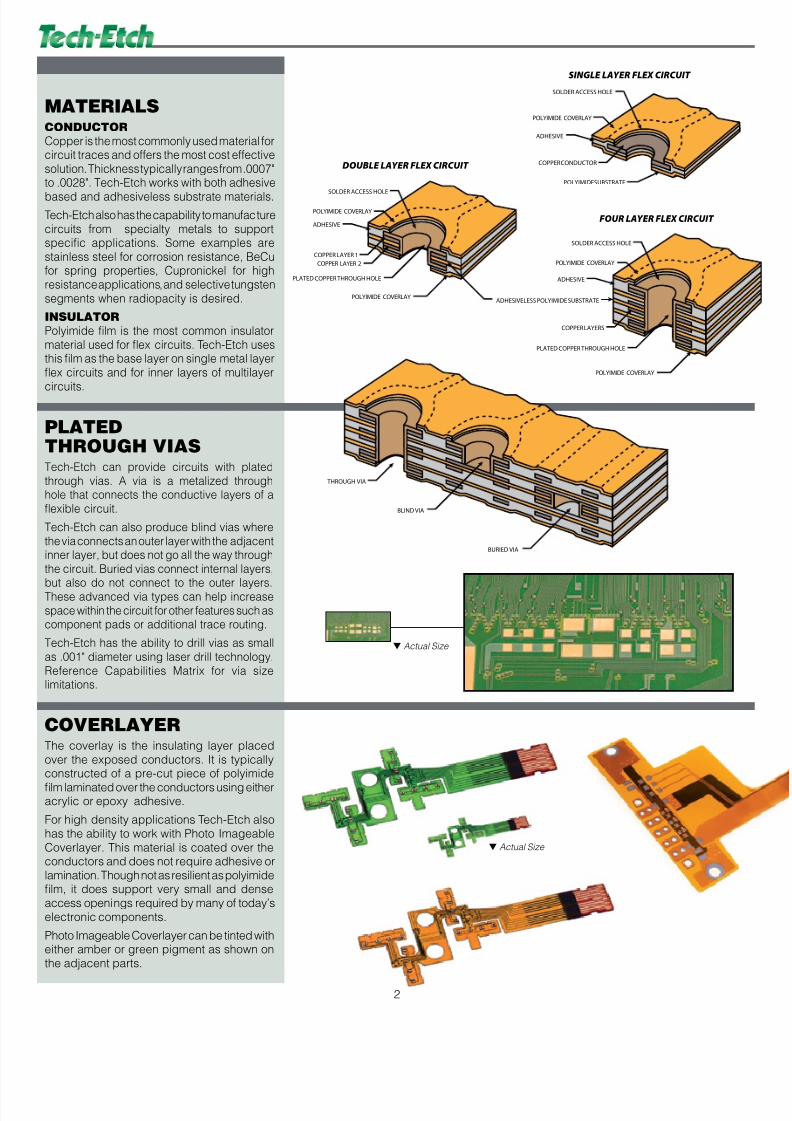
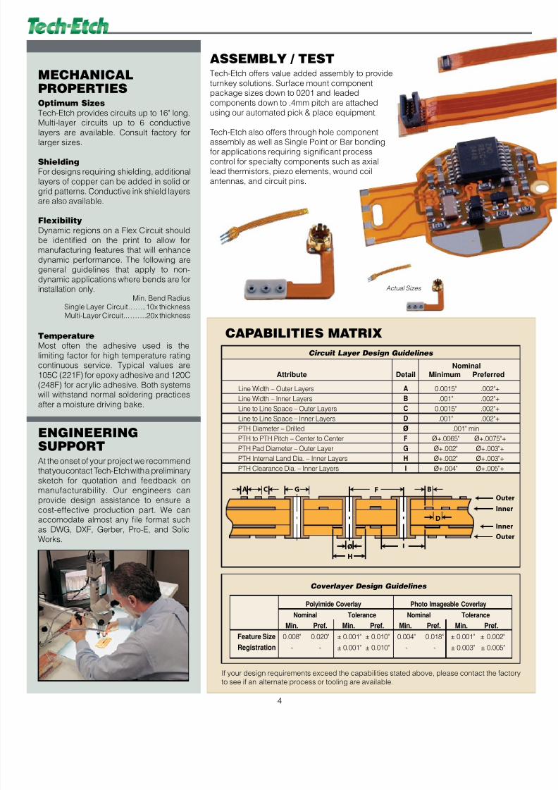
tActual Size
POLYIMIDE COVERLAY
ADHESIVE
COPPER CONDUCTOR
SOLDER ACCESS HOLE
POLYIMIDE SUBSTRATE
SINGLE LAYER FLEX CIRCUIT
MATERIALS
CONDUCTOR
Copper is the most commonly used material forcircuit traces and offers the most cost effectivesolution. Thickness typically ranges from .0007"to .0028". Tech-Etch works with both adhesive
based and adhesiveless substrate materials.Tech-Etch also has the capability to manufacturecircuits from specialty metals to supportspecific applications. Some examples arestainless steel for corrosion resistance, BeCufor spring properties, Cupronickel for highresistance applications, and selective tungstensegments when radiopacity is desired.
INSULATOR Polyimide film is the most common insulatormaterial used for flex circuits. Tech-Etch usesthis film as the base layer on single metal layerflex circuits and for inner layers of multilayer
circuits.
THROUGH VIA
BLIND VIA
BURIED VIA
tActual Size
POLYIMIDE COVERLAY
ADHESIVE
PLATED COPPER THROUGH HOLE
COPPER LAYERS
SOLDER ACCESS HOLE
POLYIMIDE COVERLAY
ADHESIVELESS POLYIMIDE SUBSTRATE
FOUR LAYER FLEX CIRCUIT POLYIMIDE COVERLAY
ADHESIVE
PLATED COPPER THROUGH HOLE
COPPER LAYER 2
SOLDER ACCESS HOLE
POLYIMIDE COVERLAY
DOUBLE LAYER FLEX CIRCUIT
COPPER LAYER 1
PLATEDTHROUGH VIAS
Tech-Etch can provide circuits with plated
through vias. A via is a metalized throughhole that connects the conductive layers of a
flexible circuit.
Tech-Etch can also produce blind vias where
the via connects an outer layer with the adjacentinner layer, but does not go all the way through
the circuit. Buried vias connect internal layers,but also do not connect to the outer layers.
These advanced via types can help increase
space within the circuit for other features such ascomponent pads or additional trace routing.
Tech-Etch has the ability to drill vias as small
as .001" diameter using laser drill technology.
Reference Capabilities Matrix for via sizelimitations.
COVERLAYER
The coverlay is the insulating layer placed
over the exposed conductors. It is typicallyconstructed of a pre-cut piece of polyimide
film laminated over the conductors using eitheracrylic or epoxy adhesive.
For high density applications Tech-Etch also
has the ability to work with Photo Imageable
Coverlayer. This material is coated over theconductors and does not require adhesive or
lamination. Though not as resilient as polyimidefilm, it does support very small and dense
access openings required by many of today’s
electronic components.
Photo Imageable Coverlayer can be tinted witheither amber or green pigment as shown on
the adjacent parts.
2

8/12/2019 Flex Design Guide
http://slidepdf.com/reader/full/flex-design-guide 3/6
8/12/2019 Flex Design Guide
http://slidepdf.com/reader/full/flex-design-guide 4/6
8/12/2019 Flex Design Guide
http://slidepdf.com/reader/full/flex-design-guide 5/6
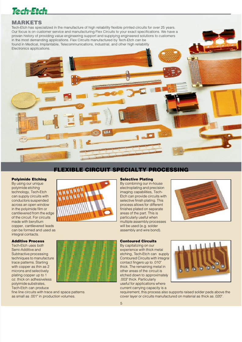
Polyimide EtchingBy using our unique
polyimide etchingtechnology, Tech-Etch
can supply circuits with
conductors suspendedacross an open window
in the polyimide film orcantilevered from the edge
of the circuit. For circuitsmade with beryllium
copper, cantilevered leads
can be formed and used asintegral contacts.
Additive Process
Tech-Etch uses bothSemi-Additive and
Subtractive processing
techniques to manufacturetrace patterns. Starting
with copper as thin as 2microns and selectively
plating copper up to 1
oz. thick on adhesivelesspolyimide substrates,
Tech-Etch can producefine line circuits with trace and space patterns
as small as .001" in production volumes.
Selective PlatingBy combining our in-house
electroplating and precisionimaging capabilities, Tech-
Etch can provide circuits with
selective finish plating. Thisprocess allows for different
finishes plated on separateareas of the part. This is
particularly useful whenmultiple assembly processes
will be used (e.g. solder
assembly and wire bond).
Contoured Circuits
By capitalizing on ourexperience with thick metal
etching, Tech-Etch can supply
Contoured Circuits with integralcontact fingers up to .010"
thick. The remaining metal inother areas of the circuit is
etched down to approximately
.003" thick. Particularlyuseful for applications where
current carrying capacity is arequirement, this process also supports raised solder pads above t
cover layer or circuits manufactured on material as thick as .020".
FLEXIBLE CIRCUIT SPECIALTY PROCESSING
5
8/12/2019 Flex Design Guide
http://slidepdf.com/reader/full/flex-design-guide 6/66
TECH-ETCH, INC., 45 Aldrin Road, Plymouth, MA 02360 • TEL 508-747-0300 • FAX 508-746-9639
The data presented in this brochure is based on testing and to our knowledge is accurate and true. Sinceapplications, test measures, and test procedures may vary, we recommend that users of our productsperform their own tests to assure the suitability of these products for their specific applications.
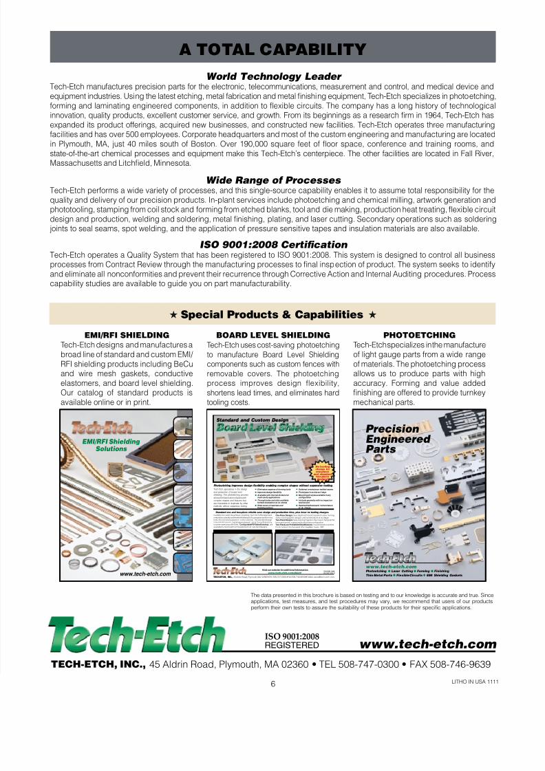
★ Special Products & Capabilities ★
ISO 9001:2008
REGISTERED www.tech-etch.com
LITHO IN USA 1111
A TOTAL CAPABILITY
World Technology Leader Tech-Etch manufactures precision parts for the electronic, telecommunications, measurement and control, and medical device and
equipment industries. Using the latest etching, metal fabrication and metal finishing equipment, Tech-Etch specializes in photoetching,
forming and laminating engineered components, in addition to flexible circuits. The company has a long history of technologicalinnovation, quality products, excellent customer service, and growth. From its beginnings as a research firm in 1964, Tech-Etch has
expanded its product offerings, acquired new businesses, and constructed new facilities. Tech-Etch operates three manufacturing
facilities and has over 500 employees. Corporate headquarters and most of the custom engineering and manufacturing are locatedin Plymouth, MA, just 40 miles south of Boston. Over 190,000 square feet of floor space, conference and training rooms, and
state-of-the-art chemical processes and equipment make this Tech-Etch’s centerpiece. The other facilities are located in Fall River,Massachusetts and Litchfield, Minnesota.
Wide Range of Processes Tech-Etch performs a wide variety of processes, and this single-source capability enables it to assume total responsibility for the
quality and delivery of our precision products. In-plant services include photoetching and chemical milling, artwork generation andphototooling, stamping from coil stock and forming from etched blanks, tool and die making, production heat treating, flexible circuit
design and production, welding and soldering, metal finishing, plating, and laser cutting. Secondary operations such as solderingjoints to seal seams, spot welding, and the application of pressure sensitive tapes and insulation materials are also available.
ISO 9001:2008 Certification Tech-Etch operates a Quality System that has been registered to ISO 9001:2008. This system is designed to control all businessprocesses from Contract Review through the manufacturing processes to final inspection of product. The system seeks to identify
and eliminate all nonconformities and prevent their recurrence through Corrective Action and Internal Auditing procedures. Processcapability studies are available to guide you on part manufacturability.
BOARD LEVEL SHIELDING
Tech-Etch uses cost-saving photoetching
to manufacture Board Level Shielding
components such as custom fences with
removable covers. The photoetching
process improves design flexibility,
shortens lead times, and eliminates hard
tooling costs.
PHOTOETCHING
Tech-Etch specializes in the manufacture
of light gauge parts from a wide range
of materials. The photoetching processallows us to produce parts with high
accuracy. Forming and value addedfinishing are offered to provide turnkey
mechanical parts.
EMI/RFI SHIELDING
Tech-Etch designs and manufactures a
broad line of standard and custom EMI/
RFI shielding products including BeCuand wire mesh gaskets, conductive
elastomers, and board level shielding.Our catalog of standard products is
available online or in print.
EMI/RFI Shielding Solutions
www.tech-etch.com
www.tech-etch.com Photoetching ● Laser Cutting ● Forming ● Finishing
Thin Metal Parts ● Flexible Circuits ● EMI Shielding Gaskets
PrecisionEngineeredParts
Tech-Etch specializes in the design
and production of board level
shielding. The photoetching process
allows the fabrication of parts with
complex shapes and features that
are impossible to duplicate by other
methods without expensive tooling.
Standard and Custom Design
Eliminates expense of forming tools
Improves design flexibility
Available with internal dividers formulti-cavity applications
Through holes and slots availableforheat dissipation at no charge
Wide range of materials andfinishing options
Soldered orresistance welded seams
Prototypes in as few as 5 days
Mounting pin styles available in anyconfiguration
Intricate geometry with no impact ontooling cost
Depthetchedlogosand nomenclature at no charge
Standard Spring Finger Cover Two-Piece Designs Standard Dimpled Cover, Low-Profile Two-Piece Designs
No toolingcharge forone-piece
and standard two-piece designs!
Photoetching improves design flexibility enabling complex shapes without expensive tooling.
In addition to custom board level shielding, Tech-Etch offersstandard
oneandtwo-pieceboardlevelshielddesigns.Byusingstandardformingtools, the cost isnot passed on to the customer. The standard design
materialsofbrassand tinplatingarealwaysin stock.Consultthefactoryforothermaterialsandfinishes. ConfigurablePDFSalesDrawings are
available for download from the website for all standard designs.
One-Piece Designs have depth-etch bend lineswhich allow forming
without tooling, aswell aslogos and nomenclature at no charge.Two-Piece Designs have a spring fingerson the covers that grab the
fence and can be customized to almost anyconfiguration.Two-PieceLow-ProfileSlimShieldDesigns havedimpledcoversthat
fit into holeson the fence and offer heightsas lowas .060”.
Standard one and two-piece shields save design and production time, plus incur no tooling charges.
TECH-ETCH, INC., 45 Aldrin Road, Plymouth, MA 02360 •TEL 508-747-0300 •FAX 508-746-9639 •E-MAIL [email protected]
Visit our website for additional information.
www.tech-etch.com/shield ISO 9001:2008
REGISTERED