Flash Translation Layer (ONFI Controller)
1
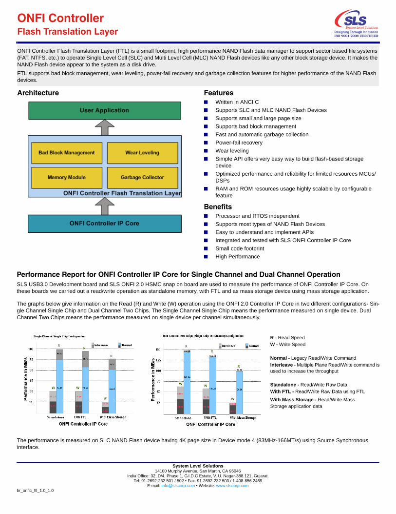
ONFI Controller Flash Translation Layer Architecture Features ■ Written in ANCI C ■ Supports SLC and MLC NAND Flash Devices ■ Supports small and large page size ■ Supports bad block management ■ Fast and automatic garbage collection ■ Power-fail recovery ■ Wear leveling ■ Simple API offers very easy way to build flash-based storage device ■ Optimized performance and reliability for limited resources MCUs/ DSPs ■ RAM and ROM resources usage highly scalable by configurable feature Benefits ■ Processor and RTOS independent ■ Supports most types of NAND Flash Devices ■ Easy to understand and implement APIs ■ Integrated and tested with SLS ONFI Controller IP Core ■ Small code footprint ■ High Performance ONFI Controller Flash Translation Layer (FTL) is a small footprint, high performance NAND Flash data manager to support sector based file systems (FAT, NTFS, etc.) to operate Single Level Cell (SLC) and Multi Level Cell (MLC) NAND Flash devices like any other block storage device. It makes the NAND Flash device appear to the system as a disk drive. FTL supports bad block management, wear leveling, power-fail recovery and garbage collection features for higher performance of the NAND Flash devices. Performance Report for ONFI Controller IP Core for Single Channel and Dual Channel Operation SLS USB3.0 Development board and SLS ONFI 2.0 HSMC snap on board are used to measure the performance of ONFI Controller IP Core. On these boards we carried out a read/write operation as standalone memory, with FTL and as mass storage device using mass storage application. R - Read Speed W - Write Speed Normal - Legacy Read/Write Command Interleave - Multiple Plane Read/Write command is used to increase the throughput Standalone - Read/Write Raw Data With FTL - Read/Write Raw Data using FTL With Mass Storage - Read/Write Mass Storage application data The performance is measured on SLC NAND Flash device having 4K page size in Device mode 4 (83MHz-166MT/s) using Source Synchronous interface. System Level Solutions 14100 Murphy Avenue, San Martin, CA 95046 India Office: 32, D/4, Phase 1, G.I.D.C Estate, V. U. Nagar-388 121, Gujarat. Tel: 91-2692-232 501 / 502 • Fax: 91-2692-232 503 / 1-408-856 2469 E-mail: [email protected] • Website: www.slscorp.com br_onfic_ftl_1.0_1.0 The graphs below give information on the Read (R) and Write (W) operation using the ONFI 2.0 Controller IP Core in two different configurations- Sin- gle Channel Single Chip and Dual Channel Two Chips. The Single Channel Single Chip means the performance measured on single device. Dual Channel Two Chips means the performance measured on single device per channel simultaneously.
-
Upload
naziag -
Category
Technology
-
view
375 -
download
6
Transcript of Flash Translation Layer (ONFI Controller)
ONFI ControllerFlash Translation Layer
Architecture Features■ Written in ANCI C
■ Supports SLC and MLC NAND Flash Devices
■ Supports small and large page size
■ Supports bad block management
■ Fast and automatic garbage collection
■ Power-fail recovery
■ Wear leveling
■ Simple API offers very easy way to build flash-based storage device
■ Optimized performance and reliability for limited resources MCUs/DSPs
■ RAM and ROM resources usage highly scalable by configurable feature
Benefits■ Processor and RTOS independent
■ Supports most types of NAND Flash Devices
■ Easy to understand and implement APIs
■ Integrated and tested with SLS ONFI Controller IP Core
■ Small code footprint
■ High Performance
ONFI Controller Flash Translation Layer (FTL) is a small footprint, high performance NAND Flash data manager to support sector based file systems (FAT, NTFS, etc.) to operate Single Level Cell (SLC) and Multi Level Cell (MLC) NAND Flash devices like any other block storage device. It makes the NAND Flash device appear to the system as a disk drive.
FTL supports bad block management, wear leveling, power-fail recovery and garbage collection features for higher performance of the NAND Flash devices.
Performance Report for ONFI Controller IP Core for Single Channel and Dual Channel OperationSLS USB3.0 Development board and SLS ONFI 2.0 HSMC snap on board are used to measure the performance of ONFI Controller IP Core. On these boards we carried out a read/write operation as standalone memory, with FTL and as mass storage device using mass storage application.
R - Read Speed
W - Write Speed
Normal - Legacy Read/Write Command
Interleave - Multiple Plane Read/Write command is used to increase the throughput
Standalone - Read/Write Raw Data
With FTL - Read/Write Raw Data using FTL
With Mass Storage - Read/Write Mass Storage application data
The performance is measured on SLC NAND Flash device having 4K page size in Device mode 4 (83MHz-166MT/s) using Source Synchronous interface.
System Level Solutions14100 Murphy Avenue, San Martin, CA 95046
India Office: 32, D/4, Phase 1, G.I.D.C Estate, V. U. Nagar-388 121, Gujarat.Tel: 91-2692-232 501 / 502 • Fax: 91-2692-232 503 / 1-408-856 2469
E-mail: [email protected] • Website: www.slscorp.combr_onfic_ftl_1.0_1.0
The graphs below give information on the Read (R) and Write (W) operation using the ONFI 2.0 Controller IP Core in two different configurations- Sin-gle Channel Single Chip and Dual Channel Two Chips. The Single Channel Single Chip means the performance measured on single device. DualChannel Two Chips means the performance measured on single device per channel simultaneously.