Firmware based Array Sorter and Matlab testing suite Final Presentation August 2011 Elad Barzilay &...
42
Firmware based Array Sorter and Matlab testing suite Final Presentation August 2011 Elad Barzilay & Uri Natanzon Supervisor: Moshe Porian
-
Upload
doris-jefferson -
Category
Documents
-
view
221 -
download
0
Transcript of Firmware based Array Sorter and Matlab testing suite Final Presentation August 2011 Elad Barzilay &...

Firmware based Array Sorter
and Matlab testing suite
Final PresentationAugust 2011
Elad Barzilay & Uri Natanzon
Supervisor: Moshe Porian
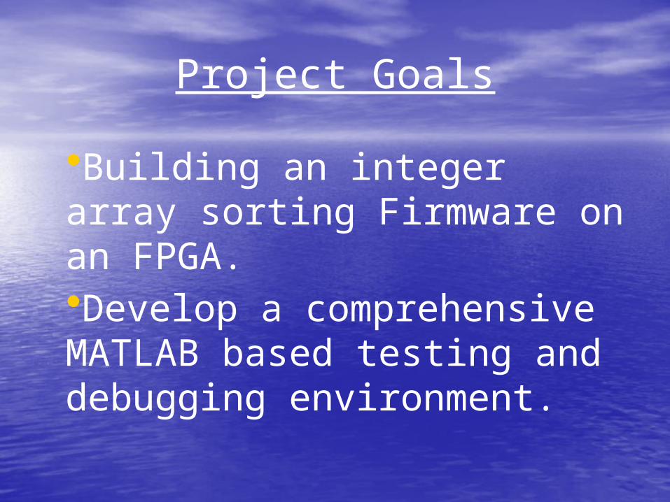
Project Goals
•Building an integer array sorting Firmware on an FPGA.•Develop a comprehensive MATLAB based testing and debugging environment.

Presentation Overview
•The need for sorting•Project Overview•Implementation review
• Sorting: Firmware• Test & debug: Software• Communication: FW & SW
•Results & demonstration
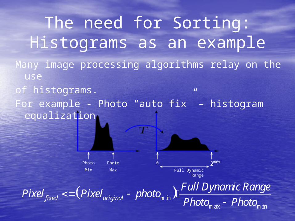
The need for Sorting:Histograms as an example
Many image processing algorithms relay on the use of histograms.For example - Photo “auto fix” – histogram equalization
minmax min
fixed original
Full Dynamic RangePixel Pixel photo
Photo Photo
Photo
Min
Photo
Max
0
Full Dynamic Range
#2 bits
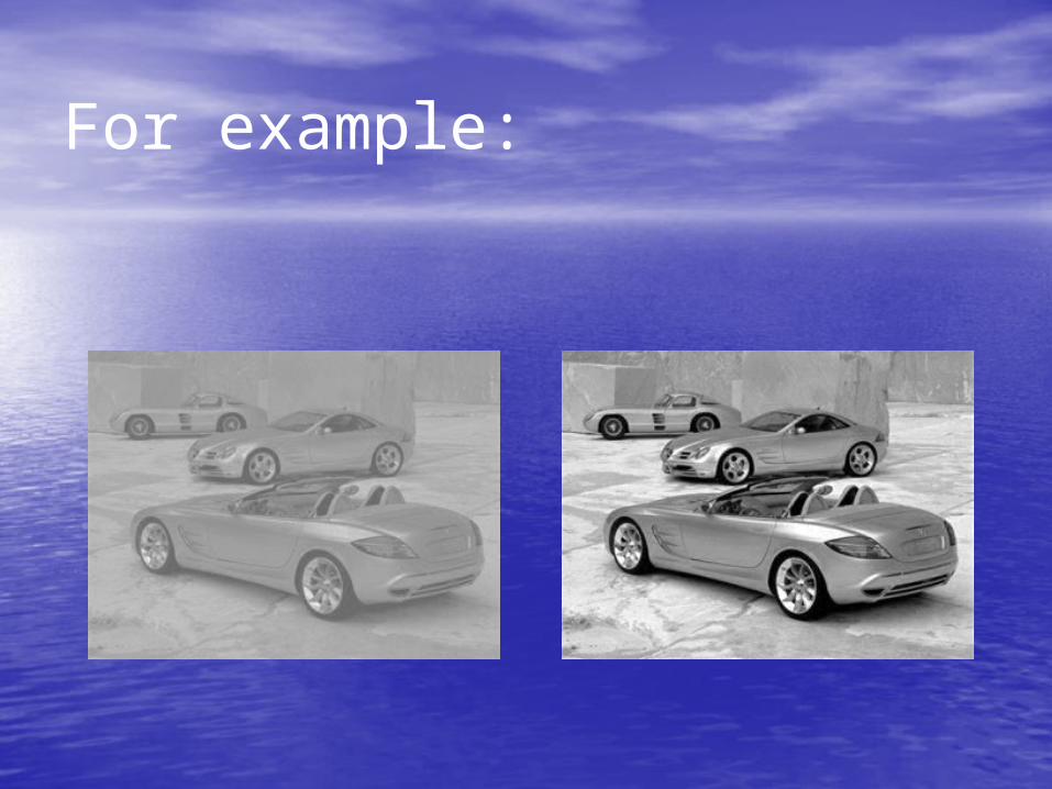
For example:
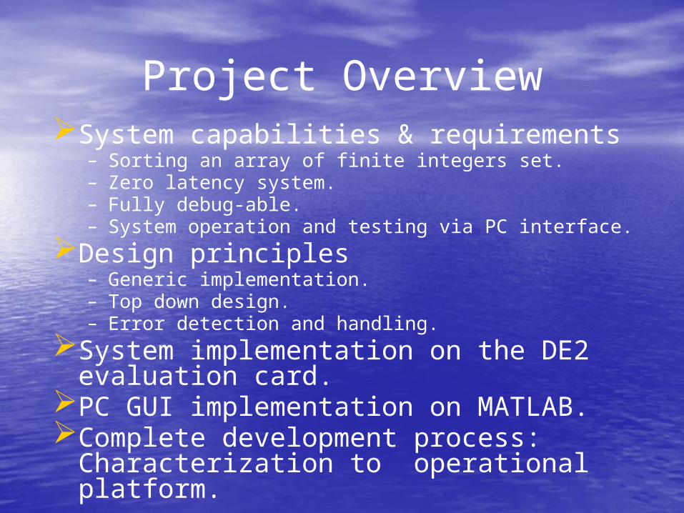
Project OverviewSystem capabilities & requirements
– Sorting an array of finite integers set.– Zero latency system.– Fully debug-able.– System operation and testing via PC interface.
Design principles– Generic implementation.– Top down design.– Error detection and handling.
System implementation on the DE2 evaluation card. PC GUI implementation on MATLAB.Complete development process: Characterization to
operational platform.
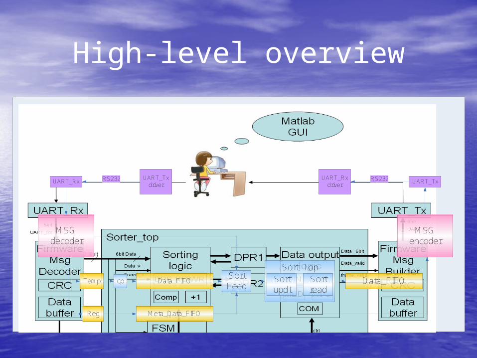
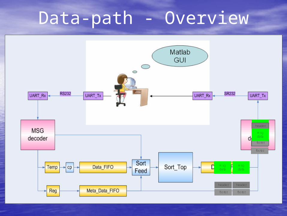
High-level overview
UART_Rx UART_TxUART_Rx
driverRS232 RS232
MSGdecoder
Data_FIFO
Meta_Data_FIFO
SortFeed
Sort_Top
MSGencoder
Data_FIFOTemp
Reg
cp Sortupdt
Sortread
UART_Txdriver
MOSHE PORIAN
שקף זה חייב להיות מלווה בהסברים מלאים בע"פ בלבד (כפי שהתכוונתם) אך ממליץ לרשום את פירוט ההסברים בשדה ה- notes (קיים במסמך הפרויקט).
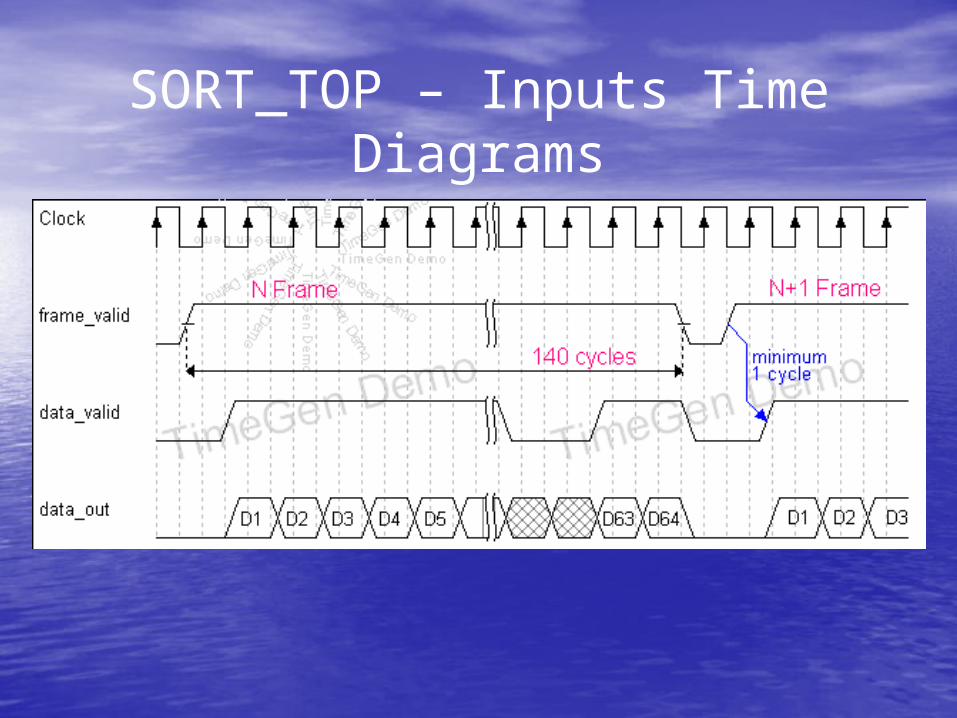
SORT_TOP – Inputs Time Diagrams

SORT_TOP – Outputs Time Diagrams
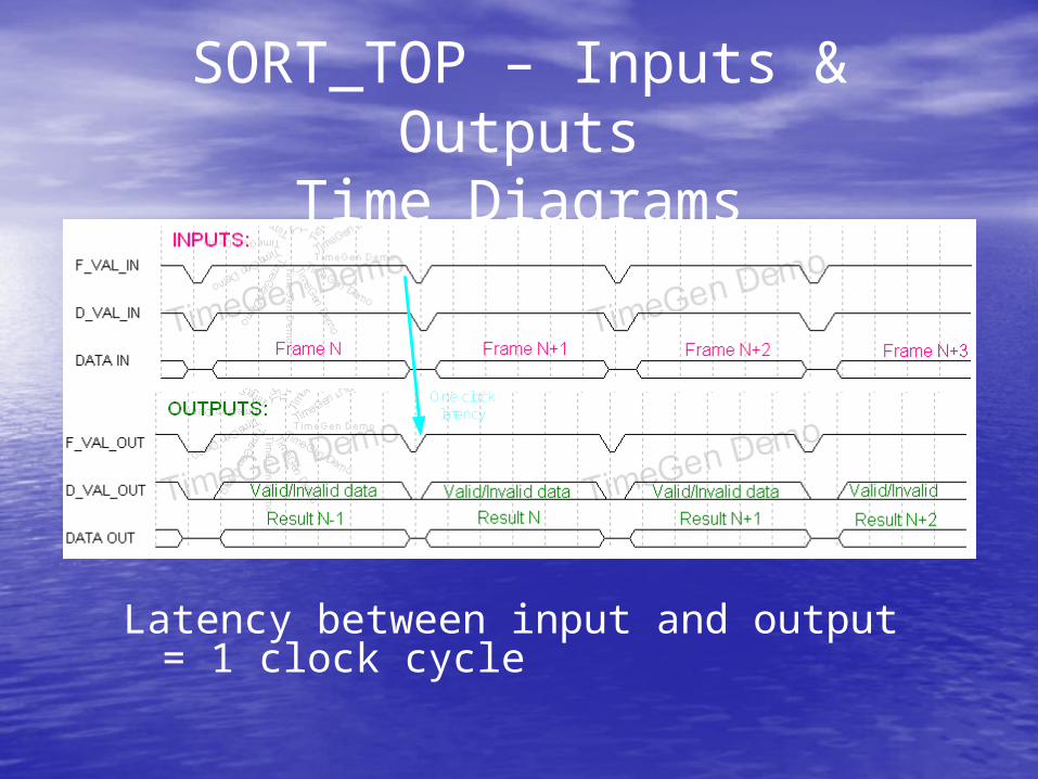
SORT_TOP – Inputs & OutputsTime Diagrams
One clock latency
Latency between input and output = 1 clock cycle
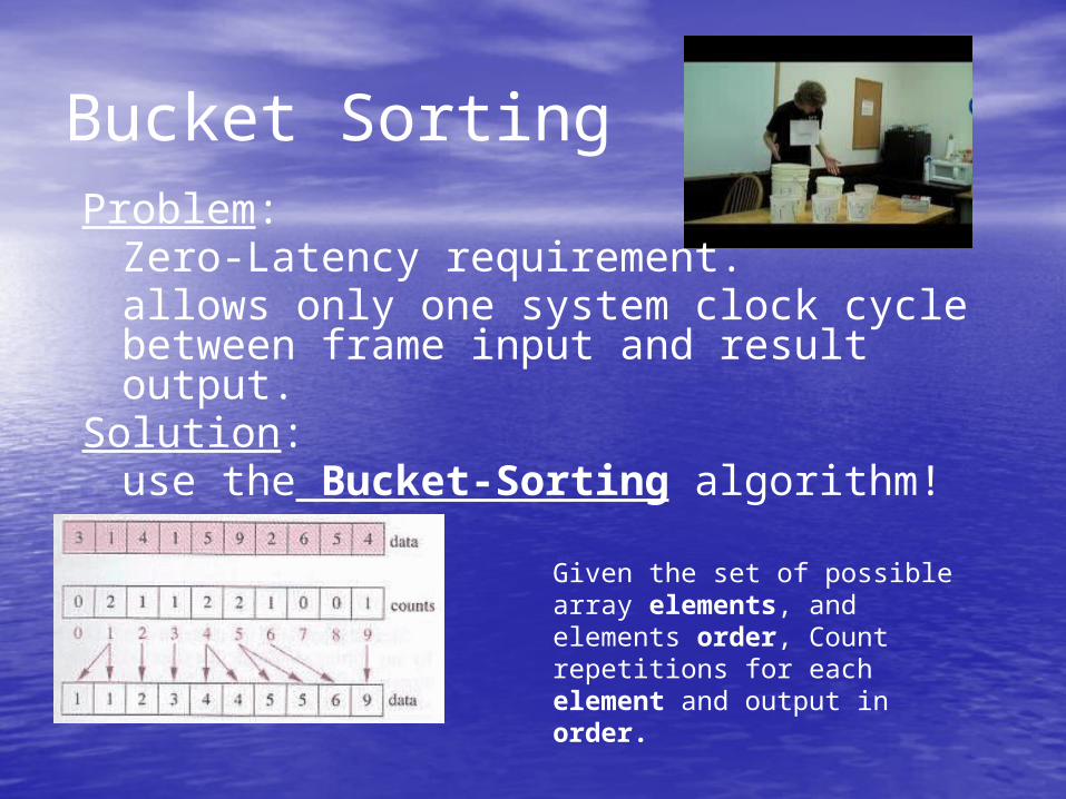
Bucket SortingProblem:
Zero-Latency requirement. allows only one system clock cycle between frame input and result output.
Solution:use the Bucket-Sorting algorithm!
Given the set of possible array elements, and elements order, Count repetitions for each element and output in order.
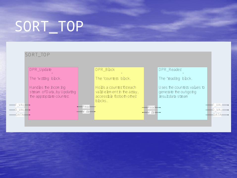
SORT_TOP
SORT_TOP
DPR_Reader
The “reading” block.
Uses the counters values to generate the out-going result data stream
DPR_Block
The “counters” block.
Holds a counter for each valid element in the array, accessible for both other blocks.
DPR_Update
The “writing” block.
Handles the incoming stream of Data, by Updating the appropriate counter.
F_VAL
DATA
D_VALRead
WriteRead
Write
F_VAL
DATA
D_VAL
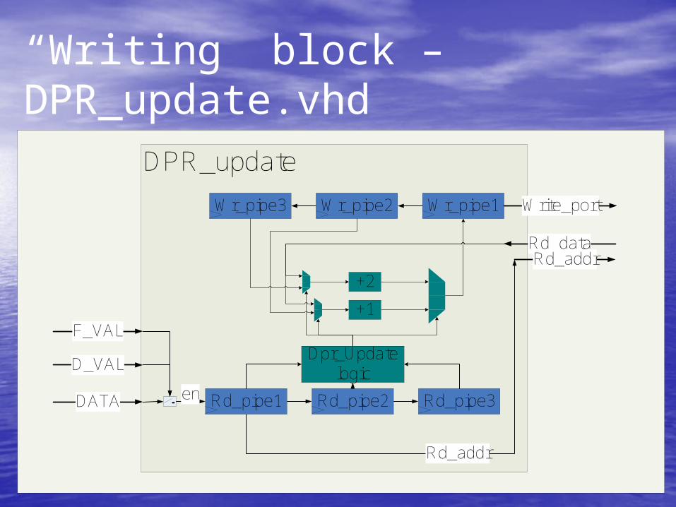
DPR_update
F_VAL
DATA
D_VAL
en
Rd_addr
Rd_pipe1 Rd_pipe2 Rd_pipe3
Wr_pipe3 Wr_pipe2 Wr_pipe1 Write_port
Rd_data
Dpr_Updatelogic
+1
+2Rd_addr
“Writing” block – DPR_update.vhd
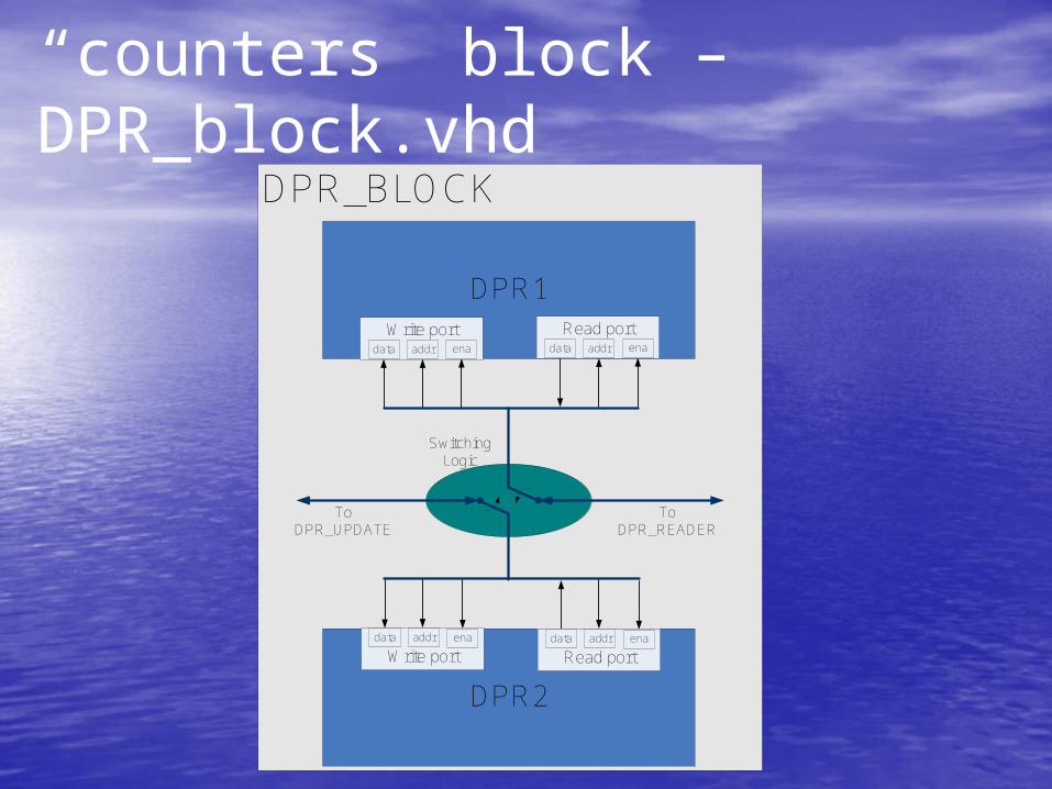
“counters” block –DPR_block.vhd
DPR_BLOCK
DPR1Write port
DPR2
SwitchingLogic
To DPR_READER
To DPR_UPDATE
data addr ena
Read portdata addr ena
Write portdata addr ena
Read portdata addr ena
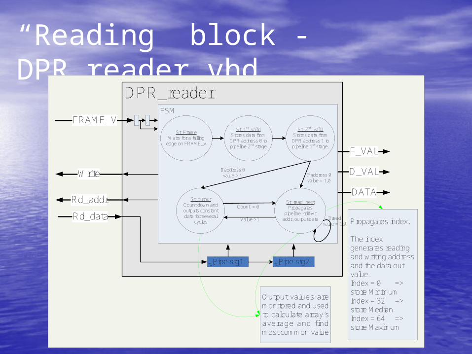
“Reading” block - DPR_reader.vhd
DPR_reader
F_VAL
DATA
Write
Rd_addr
D_VAL
FRAME_VFSM
St_FrameWaits for a falling
edge on FRAME_V
St_1st_validStores data from DPR address 0 to pipeline 2nd stage
St_2nd_validStores data from DPR address 1 to pipeline 1st stage.
St_outputCount down and outputs constant data for several
cycles
St_read_nextPropagates
pipeline -rd&wr addr, output data
If address 0 value > 1 If address 0
value = 1,0
Count = 0
Value >1 If read value = 1,0
Pipe stg1 Pipe stg2
Rd_dataPropagates index.
The index generates reading and writing address and the data out value.Index = 0 => store MinimumIndex = 32 => store MedianIndex = 64 => store Maximum
Output values are monitored and used to calculate array’s average and f ind most common value
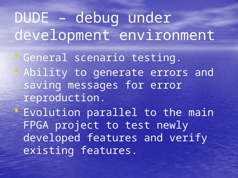
DUDE – debug under development environment• General scenario testing.• Ability to generate errors and saving
messages for error reproduction. • Evolution parallel to the main FPGA
project to test newly developed features and verify existing features.

“DUDE” – Debugging Under Development Environment
MATLAB based GUI for data injection and result validation

“DUDE” – connection generation and main features
Reloading last sent messages
Serial port and CRC control
Consecutive message sending: Random or GUI-screen generated messages.
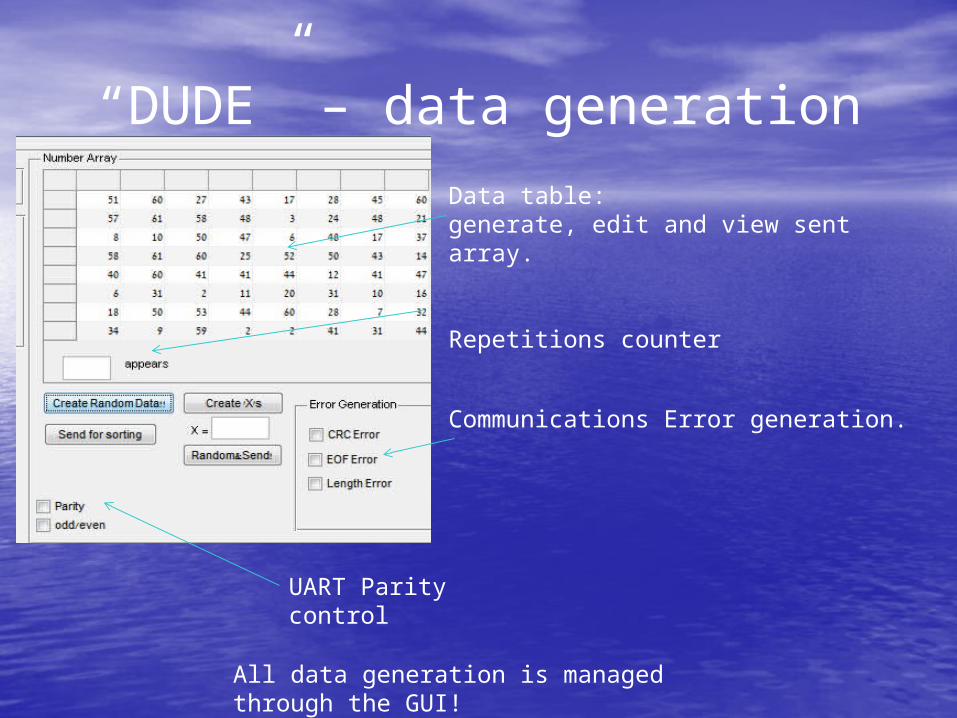
“DUDE” – data generation
Communications Error generation.
UART Parity control
Data table:generate, edit and view sent array.
Repetitions counter
All data generation is managed through the GUI!
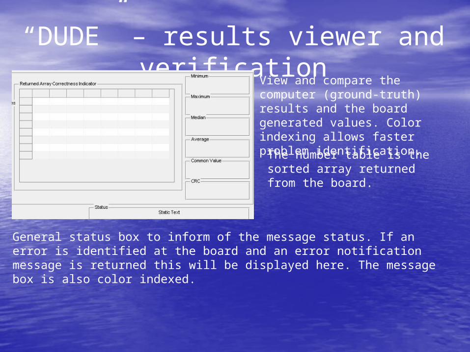
“DUDE” – results viewer and verification
The number table is the sorted array returned from the board.
General status box to inform of the message status. If an error is identified at the board and an error notification message is returned this will be displayed here. The message box is also color indexed.
View and compare the computer (ground-truth) results and the board generated values. Color indexing allows faster problem identification.
“DUDE” – implementation guidelines
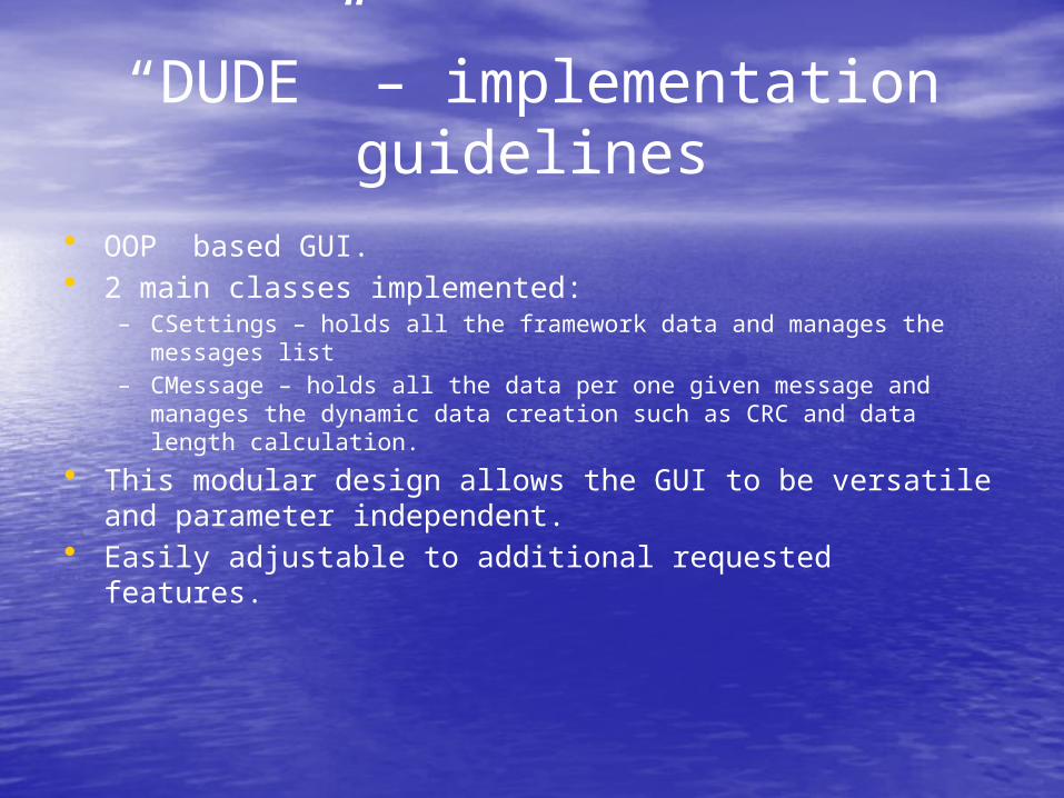
• OOP based GUI.• 2 main classes implemented:
– CSettings – holds all the framework data and manages the messages list
– CMessage – holds all the data per one given message and manages the dynamic data creation such as CRC and data length calculation.
• This modular design allows the GUI to be versatile and parameter independent.
• Easily adjustable to additional requested features.
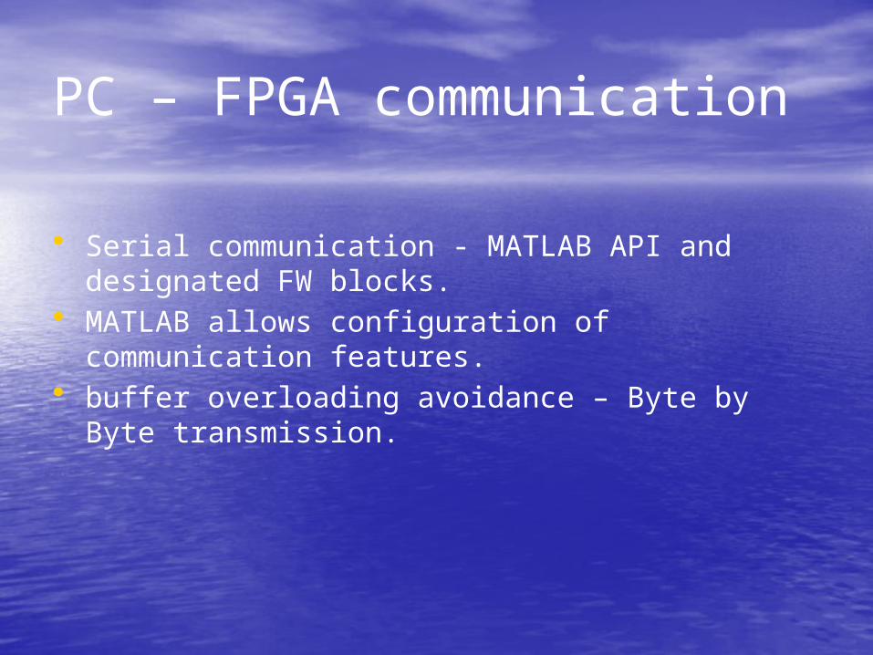
PC – FPGA communication
• Serial communication - MATLAB API and designated FW blocks.
• MATLAB allows configuration of communication features.
• buffer overloading avoidance – Byte by Byte transmission.
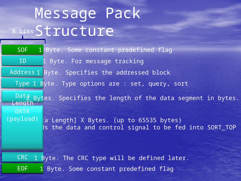
Message Pack Structure
SOF
ID
Data Length
CRC
EOF
8 bits
1 Byte. Some constant predefined flag
1 Byte. For message tracking
2 Bytes. Specifies the length of the data segment in bytes.
1 Byte. The CRC type will be defined later.
1 Byte. Some constant predefined flag
Address 1 Byte. Specifies the addressed block
Type 1 Byte. Type options are : set, query, sort
[Data Length] X Bytes. (up to 65535 bytes)Holds the data and control signal to be fed into SORT_TOP
DATA(payload)
Queuing system
• PC messages – 115200 bits/second• Firmware clock – 60 MHz.
– Firmware is much faster…
To allow testing of consecutive inputs a queuing system is required…
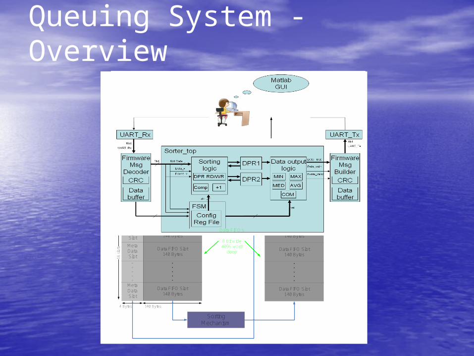
Queuing System - Overview
HeaderID, Type etc.
(5 Bytes)
CRC
Msg Data (140 Bytes)
4 Bytesregister
Temporary Data FIFO256 Bytes deep
ValidityCheck logic
SOF
EOF
Meta DataSlot
140 Bytes4 Bytes
16 s
lots
Data FIFO Slot140 Bytes
Data FIFO Slot140 Bytes
Data FIFO Slot140 Bytes
Data FIFO Slot140 Bytes
Meta DataSlot
Meta DataSlot
Meta DataSlot
Copy?Copy?
SortingMechanism
Data FIFO Slot140 Bytes
Data FIFO Slot140 Bytes
Data FIFO Slot140 Bytes
Data FIFO Slot140 Bytes
HeaderID, Type etc.
(5 Bytes)
CRC
Msg Data (140 Bytes)SOF
EOF
Encodinglogic
Data FIFO’s
8 bit wide4096 word
deep
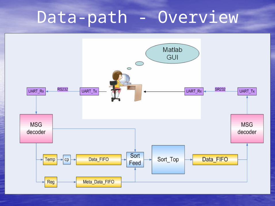
Data-path - Overview
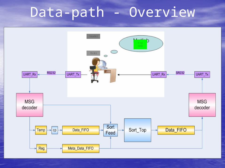
msgdata
header
footer
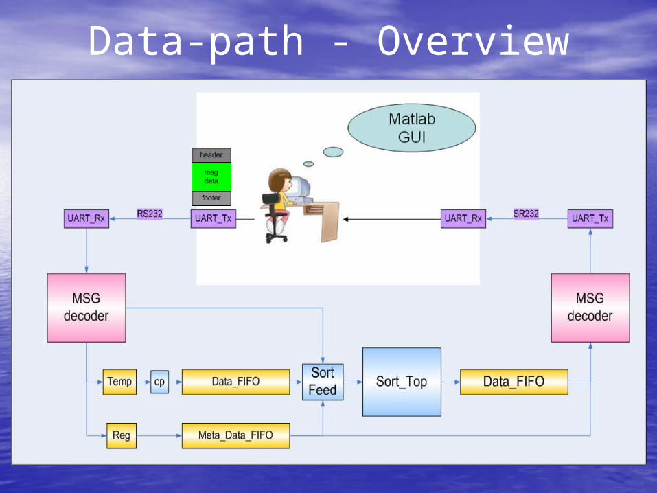
Data-path - Overview

msgdata
header
footer
Data-path - Overview
Data-path - Overview

header
footer
msgdata
Data-path - Overview
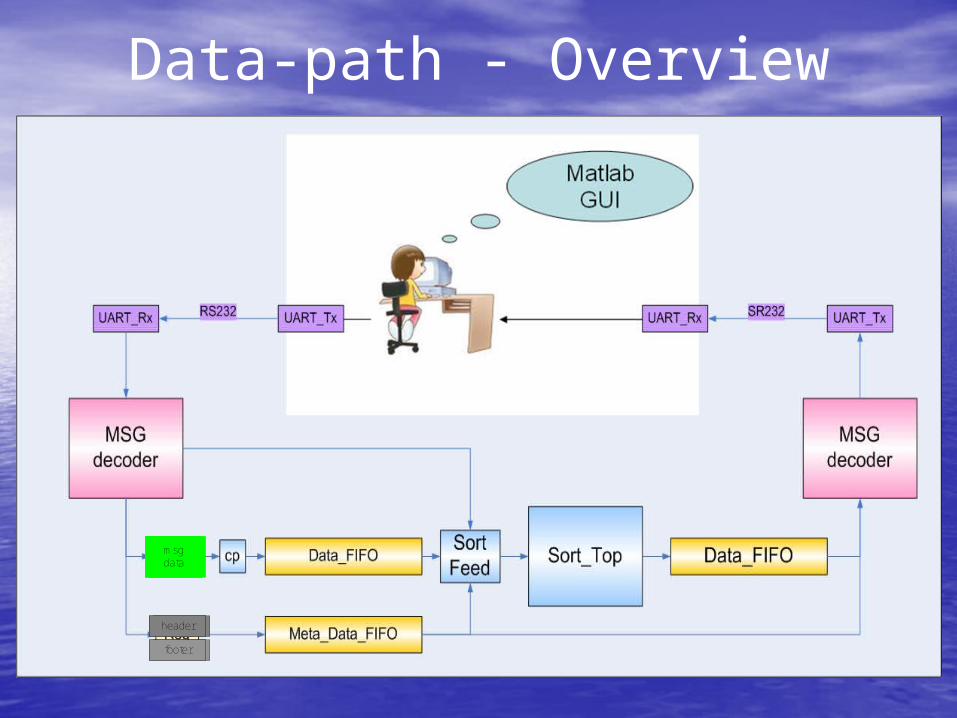
footer
header
msgdata
footer
header
msgdata
footer
header
msgdata
Data-path - Overview

footer
header
msgdata
footer
header
msgdata
footer
header
msgdata
Done
Data-path - Overview

footer
header
msgdata
footer
header
msgdata
footer
header
msgdata
Data-path - Overview
footer
header
msgdata
footer
header
msgdata
footer
header
msgdata
footer
header
msgdata
footer
header
msgdata
footer
header
msgdata
Data-path - Overview

Data-path - Overview
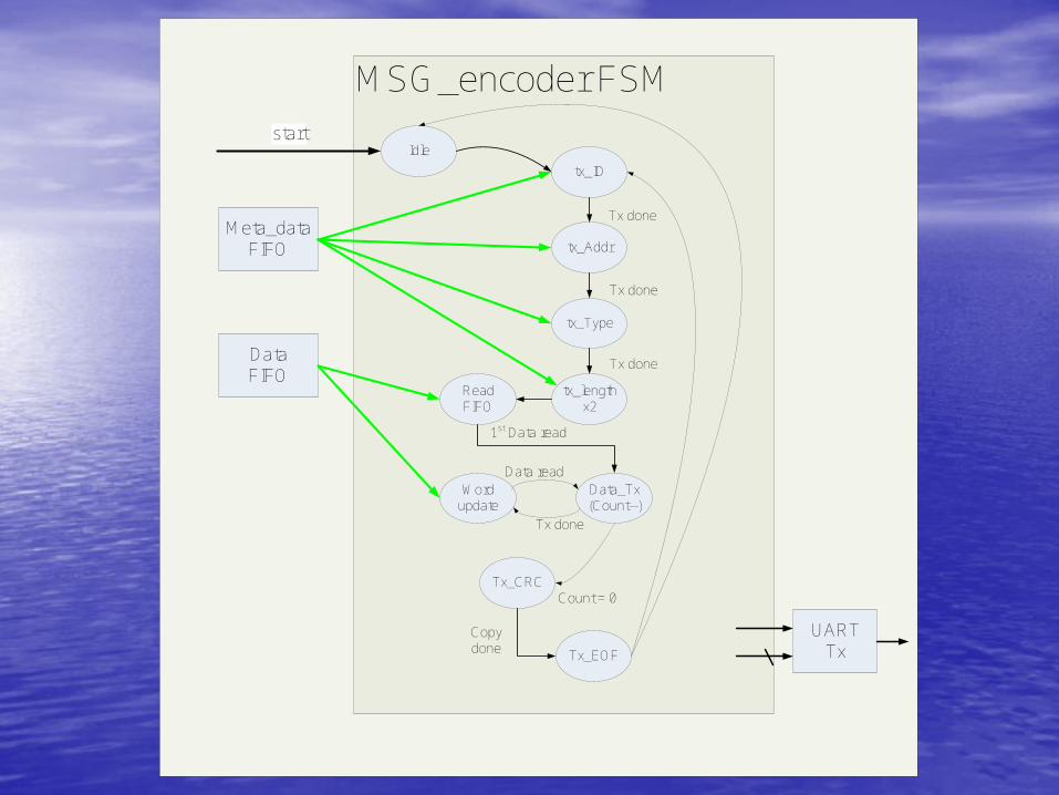
MSG_encoder FSM
UARTTx
Idle
tx_Addr
tx_ID
tx_Type
ReadFIFO
tx_lengthx2
Data_Tx(Count--)
Tx_CRC
Wordupdate
Tx_EOF
Tx done
Copy done
Meta_dataFIFO
DataFIFO
start
Tx done
Data read
1st Data read
Count = 0
Tx done
Tx done
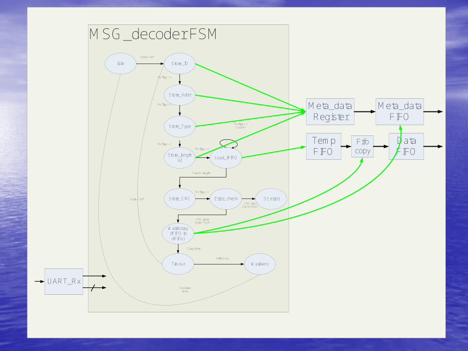
MSG_decoder FSM
UART_Rx
Idle
Store_Addr
Store_ID
Store_Type
Load_tFIFOStore_length
x2
Store_CRC
Wait4copy(tFIFO to dFIFo)
Error_check
Timout
St_error
Wait4enc
Data = sof
Rx flag = 1
Rx flag = 1
Rx flag = 1
Rx flag = 1
Rx flag = 1Count++
Count = length
Rx flag = 1
CRC err /DATA!=EOF
CRC goodData = EOF
Copy done
After 1 ms
Data = sof
TempFIFO
DataFIFO
Fifocopy
Meta_dataFIFO
Meta_dataRegister
Encoder done
Tested scenarios
• Sorting system:– Basic test – random consecutive array.– Constant arrays.– Rising / Falling arrays.– Fast toggling.– Boundary values – zeros and 63’s in the array.
• Communication:– CRC errors.– EOF / SOF errors.– UART parity error.– Buffers overloading.
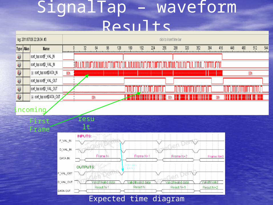
SignalTap – waveform Results
FirstFrame
incomingresul
t
One clock latency
Expected time diagram
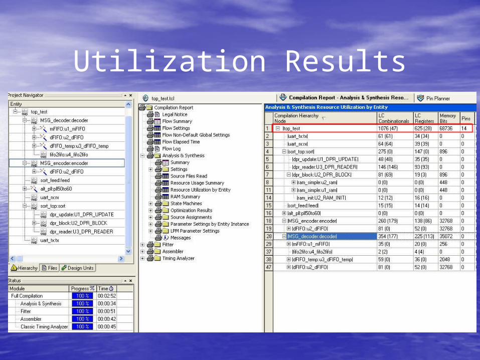
Utilization Results
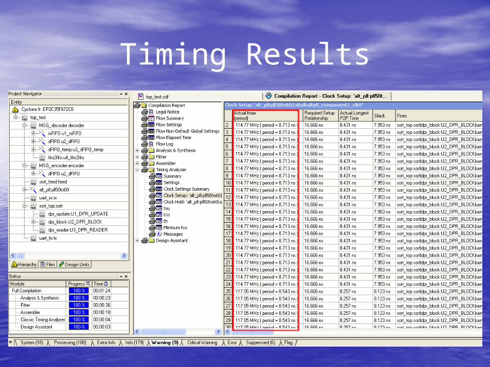
Timing Results
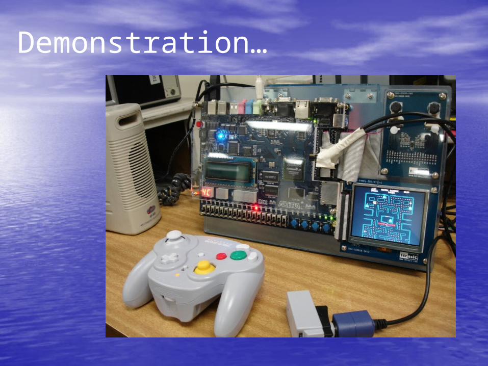
Demonstration…


![Jacob Eisenstein · [13]Tahira Naseem, Benjamin Snyder, Jacob Eisenstein and Regina Barzilay. Multilingual part-of-speech tagging: Two unsupervised approaches. Journal of Artificial](https://static.fdocuments.in/doc/165x107/5e7401d20f855c31a07dd8bb/jacob-eisenstein-13tahira-naseem-benjamin-snyder-jacob-eisenstein-and-regina.jpg)