
Finite Element Modeling Predicts the Effects of Voids on...
8
Finite Element Modeling Predicts the Effects of Voids on Thermal Shock Reliability and Thermal Resistance of Power Device The thermal-mechanical effects of void size and location in lead-free solder heat-sink attachment of power devices is investigated BY J. CHANG, L. WANG, J. DIRK, AND X. XIE ABSTRACT. Three-dimensional finite el- ement modeling (FEM) analysis was con- ducted to investigate the effects of the void size and location on the reliability of Sn-Ag-Cu heat-sink attachment. The re- sults showed that void size does not have a significant effect on the strain/stress dis- tribution, unless it is near the corner of the solder attachment, a location originally with higher stress. This is generally in agreement with the experimental results that a heat-sink attachment with an aver- age of 37.5% void can survive more than 3000 cycles of thermal shock at -40° to 125°C. The void size had a significant ef- fect on thermal dissipation. A 20% voids would cause the chip temperature to rise more than 5.1°C, which would obviously degrade the reliability of the device. Com- pared to void size, the location of voids is less significant. Void size of 10% at a dif- ferent location causes chip temperature variation around 1°C. Introduction The reliability of the semiconductor de- vices is critical for designers and manufac- turers. Electronic power devices are devel- oped with increasing power capability, high voltage, and high current (Ref. 1). The typical loads for electronic power de- vices are high temperatures and tempera- ture changes. As reported, in a typical power device, 4% of controlled power is dissipated as heat in the device. So thermal and thermal-mechanical management is important for power devices (Ref. 1). In a power device assembly, materials with different thermal and mechanical properties are bonded together to consti- J. CHANG (changjunling(a>yahoo.com.cn), L. WANG, J. DIRK, and X. XIE are with Daimler- Chrysler SIM Technology Co., Ltd., Shanghai, P. R. China. CHANG and XIE are also with Shang- hai Institute of Microsystem and Information Technology, Chinese Academy of Science, Shang- hai, R R. China. tute a complicated system. The cyclic stress/strain will be produced in the as- sembly due to the coefficient of thermal expansion (CTE) mismatch of different layers during operation (Ref. 2). Soft sol- der is often used for the heat-sink attach- ment because it has very good mechanical and heat dissipation performance; also, it allows plastic deformation, so that stresses due to temperature excursions and CTE mismatches during device service can be relaxed (Ref. 3). But accumulations of the plastic deformation may produce solder fatigue cracks and eventually cause the failure of the solder attachment. Reliability of the most commonly used Sn-Pb eutectic solder has been extensively investigated and has been well under- stood. However, due to environmental and health concerns, Sn-Pb eutectic solder is being replaced by lead-free solders, among which Sn-Ag-Cu is the dominant candidate for use in reflow soldering tech- nology (Ref. 4). Although quite a large number of studies have concentrated on this new alloy system from laboratory re- search to small-scale production, more data are needed before a solid under- standing can be established. Voids are easily formed in the solder joint. It became a more critical problem when lead-free solder was used in recent years because of its comparatively poor solderability. Voids are formed due to the outgassing of flux entrapped in the solder KEYWORDS Voids Sn-Ag-Cu Thermal Shock Equivalent Plastic Strain Equivalent Stress Thermal Resistance joint during reflow (Ref. 5). The solder paste contains 35—65 vol-% volatile ma- terials. The outgassing is generally pro- duced by the evaporation of solvent and additives in the solder paste. Some gases may be entrapped between the printed circuit board (PCB) and compo- nents causing voids to be formed during cooling. Previous studies have indicated that the reflow process and solder materi- als are the most significant factors that af- fect void formation (Refs. 6, 7). There are no universal criteria regard- ing void size and location (Ref. 8). The fac- tors that affect void formation are com- plex, and it is difficult to study the effect of void on reliability because many variables in the assembly process are not control- lable regarding void formation. Most stud- ies about the effect of voids on reliability are focused on Sn-Pb eutectic solder in BGA/CSP joints (Refs. 8, 9). The results show that big voids, especially when the voids are greater than 50% of the solder joint area, had been considered one of the critical issues in joint strength and relia- bility. Small voids also have effects on re- liability, but it is dependent on the number and location. From the thermal point of view, voids in solder layers become one of the main defects affecting the heat dissipation (Ref. 10). The overall effect of voids is to de- crease the solder cross-section area avail- able for heat dissipation. The heat dissi- pation is especially important for power devices. Industrial practices often set 10% voids as the highest limit for general heat- sink attachment and 5% for higher requirements. This paper investigates the effect of void size and location in Sn-Ag-Cu heat- sink attachment on the thermal shock re- liability and thermal resistance of power devices using 3-D finite element modeling (FEM). The degradation of heat-sink at- tachment by SnAgCu lead-free solder dur- ing thermal shock has been verified by ex- periment. Samples with high voiding percentages were selected for the investi- WELDING JOURNAL
Transcript of Finite Element Modeling Predicts the Effects of Voids on...

Finite Element Modeling Predicts the Effects of Voids on Thermal Shock Reliability and
Thermal Resistance of Power Device The thermal-mechanical effects of void size and location in lead-free solder
heat-sink attachment of power devices is investigated
BY J. CHANG, L. WANG, J. DIRK, AND X. XIE
ABSTRACT. Three-dimensional finite element modeling (FEM) analysis was conducted to investigate the effects of the void size and location on the reliability of Sn-Ag-Cu heat-sink attachment. The results showed that void size does not have a significant effect on the strain/stress distribution, unless it is near the corner of the solder attachment, a location originally with higher stress. This is generally in agreement with the experimental results that a heat-sink attachment with an average of 37.5% void can survive more than 3000 cycles of thermal shock at -40° to 125°C. The void size had a significant effect on thermal dissipation. A 20% voids would cause the chip temperature to rise more than 5.1°C, which would obviously degrade the reliability of the device. Compared to void size, the location of voids is less significant. Void size of 10% at a different location causes chip temperature variation around 1°C.
Introduction
The reliability of the semiconductor devices is critical for designers and manufacturers. Electronic power devices are developed with increasing power capability, high voltage, and high current (Ref. 1). The typical loads for electronic power devices are high temperatures and temperature changes. As reported, in a typical power device, 4% of controlled power is dissipated as heat in the device. So thermal and thermal-mechanical management is important for power devices (Ref. 1).
In a power device assembly, materials with different thermal and mechanical properties are bonded together to consti-
J. CHANG (changjunling(a>yahoo.com.cn), L. WANG, J. DIRK, and X. XIE are with Daimler-Chrysler SIM Technology Co., Ltd., Shanghai, P. R. China. CHANG and XIE are also with Shanghai Institute of Microsystem and Information Technology, Chinese Academy of Science, Shanghai, R R. China.
tute a complicated system. The cyclic stress/strain will be produced in the assembly due to the coefficient of thermal expansion (CTE) mismatch of different layers during operation (Ref. 2). Soft solder is often used for the heat-sink attachment because it has very good mechanical and heat dissipation performance; also, it allows plastic deformation, so that stresses due to temperature excursions and CTE mismatches during device service can be relaxed (Ref. 3). But accumulations of the plastic deformation may produce solder fatigue cracks and eventually cause the failure of the solder attachment.
Reliability of the most commonly used Sn-Pb eutectic solder has been extensively investigated and has been well understood. However, due to environmental and health concerns, Sn-Pb eutectic solder is being replaced by lead-free solders, among which Sn-Ag-Cu is the dominant candidate for use in reflow soldering technology (Ref. 4). Although quite a large number of studies have concentrated on this new alloy system from laboratory research to small-scale production, more data are needed before a solid understanding can be established.
Voids are easily formed in the solder joint. It became a more critical problem when lead-free solder was used in recent years because of its comparatively poor solderability. Voids are formed due to the outgassing of flux entrapped in the solder
KEYWORDS
Voids Sn-Ag-Cu Thermal Shock Equivalent Plastic Strain Equivalent Stress Thermal Resistance
joint during reflow (Ref. 5). The solder paste contains 35—65 vol-% volatile materials. The outgassing is generally produced by the evaporation of solvent and additives in the solder paste. Some gases may be entrapped between the printed circuit board (PCB) and components causing voids to be formed during cooling. Previous studies have indicated that the reflow process and solder materials are the most significant factors that affect void formation (Refs. 6, 7).
There are no universal criteria regarding void size and location (Ref. 8). The factors that affect void formation are complex, and it is difficult to study the effect of void on reliability because many variables in the assembly process are not controllable regarding void formation. Most studies about the effect of voids on reliability are focused on Sn-Pb eutectic solder in BGA/CSP joints (Refs. 8, 9). The results show that big voids, especially when the voids are greater than 50% of the solder joint area, had been considered one of the critical issues in joint strength and reliability. Small voids also have effects on reliability, but it is dependent on the number and location.
From the thermal point of view, voids in solder layers become one of the main defects affecting the heat dissipation (Ref. 10). The overall effect of voids is to decrease the solder cross-section area available for heat dissipation. The heat dissipation is especially important for power devices. Industrial practices often set 10% voids as the highest limit for general heat-sink attachment and 5% for higher requirements.
This paper investigates the effect of void size and location in Sn-Ag-Cu heat-sink attachment on the thermal shock reliability and thermal resistance of power devices using 3-D finite element modeling (FEM). The degradation of heat-sink attachment by SnAgCu lead-free solder during thermal shock has been verified by experiment. Samples with high voiding percentages were selected for the investi-
WELDING JOURNAL
iVHU M:=W=M:M
Molding compound \
\ s 1 u--
Die
Die attach
f^^"^ SnAgCu
Cu heat-sink
FR4 printed circuit board
heat-sink attach FR4 printed circuit board
Mounding I compound 1
3lN Cuheatsink 1
SnAgCu I heat-sink attach |
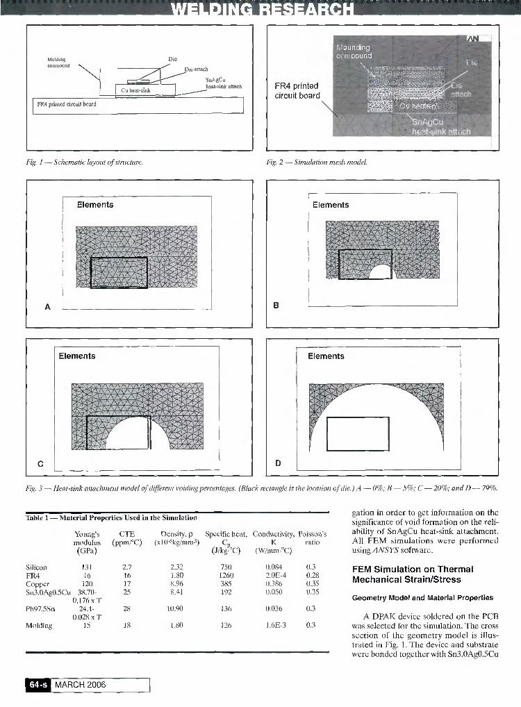
.F/g. / — Schematic layout of structure. Fig. 2 — Simulation mesh model.
Elements
NSHl :fS2SZW5SSI?5A
Elements
>•• i : < ; . \ ' V : " ' : 7 :
V:-
: : Hi
Elements
I
Isil "*8PF7:
1 Elements
w f
'*J<3<QZ
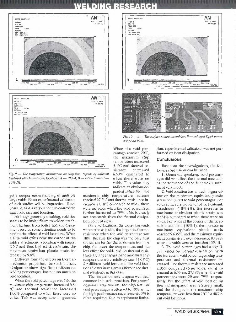
1 F/g. 3 — Heat-sink attachment model of different voiding percentages. (Black rectangle is the location of die.) A — 0%; B — 5%; C — 20%; and D — 79%.
Table 1 -
Silicon FR4 Copper
-Mi
Sn3.0Ag0.5G
Pb97.5Sn
Molding
E22
iterial Properties Used in
Young's modulus (GPa)
131 16
120 i 38.70-
0.176 x T 24.1-
0.028 x T 15
MARCH 2006
CTE (ppm/°C)
2.7 16 17 25
28
18
the Simulation
Density, p (xl0-(lkg/mm;!)
2.32 1.80 8.96 8.41
10.90
1.80
Specific heat, C P
(J/kg-°C)
750 1260 385 192
136
126
Conductivity, K
(W/mm°C)
0.084 2.0E-4 0.386 0.050
0.036
1.6E-3
Poisson's ratio
0.3 0.28 0.35 0.35
0.3
0.3
gation in order to get information on the significance of void formation on the reliability of SnAgCu heat-sink attachment. All FEM simulations were performed using^ASKS software.
FEM Simulation on Thermal Mechanical Strain/Stress
Geometry Model and Material Properties
A DPAK device soldered on the PCB was selected for the simulation. The cross section of the geometry model is illustrated in Fig. 1. The device and substrate were bonded together with Sn3.0Ag0.5Cu

i l l l l l l l i l S I I I I I I
Hfl̂ ^HHHHHHHHHRH^S •VJ=H»JL'M;I4H=M;M!
Elements
150
2^100
1 50 Q. E
( t -50
1
50
i
r~
100 150
Time(min)
200 2 50
Fig. 4 — Heat-sink attachment model with voiding percentage of10% at different locations. (Black rectangle is the location of die.) A — 10%-U; B — 70%-//; and C — 10%-Ul.
Fig. 5 — Cycles of temperature loading of simulation.
heat-sink attachment. Inside the package, a high lead solder Pb97Sn3 was used for die attachment. Since Sn3.0Ag0.5Cu solder and die attach Pb97Sn3 solder are vis-coplastic in nature, the viscoplastic Anand model was used to present the Sn3.0Ag0.5Cu solder and die attach Pb97.5Sn solder behavior. All the other materials are considered to be clastic. Material properties used in this simulation are shown in Table 1 (Ref. 11). For Sn3.0Ag0.5Cu and Pb97Sn3 solder, material properties used in the Anand model are shown in Table 2 (Ref. 11).
Meshing Model and Loading Condition
Meshing Model
In this study, 3D-l/2th symmetric models were used. All voids in the heat-sink at
tachment were assumed to be circular and leads in the package were ignored for simplification. The mesh model is shown in Fig. 2. The geometry data were directly taken from a cross section of real specimen measurements.
The heat-sink attachment model with different void sizes and locations is shown in Figs. 3 and 4, respectively. The voiding percentages 5, 10, and 20% were selected as levels of interests, and a 79% void selected as a worst case reference. For 10% voids, three typical locations were chosen for the modeling and simulation.
Loading Conditions
Room temperature was taken as the zero stress point. It is assumed that viscoplastic deformations take place at all nonzero stress values. Figure 5 shows the
Table 2 — I1
Material parameters
A (sec1) QIR (°K) % m s (MPa) n /*()(MPa) a s0 (MPa)
arameters Used in
Sn3.0Ag0.5Cu
5.87 x 10'' 7460 2.00
0.0942 58.3 0.015 9350 1.50 45.9
Anand Model
Pb97Sn3
3.25 x 10⁴
15600 7.00
0.0143 72.7
0.00437 1790 3.73 15.1
cycles of temperature loading of the simulation. The start of thermal loading was at the stress-free state of 25°C. The dwell time at -40° and 125°Cwas 15and75min, respectively. The ramp rate was 50°C/min.
WELDING JOURNAL W:

iVHUIJM:l=M=M:M! HOM.L SOLUIIOH
STIP-8
Position 1 IPPJ.IOV (AVCJ x EMX ». 009234 / ^ 5HX - . 0 0 2 0 ^ ^
A N A N
Position 1
ECDAL EQLUIroH
BTEP"B SUB =3
MPLKJV (AV&t
AN
Position 1 I N ) <AV5i V
r -.Q0133S f
• • • • • • • " • .
i?"
A N
IPPLBOV DMX «. D091D7 SDK -.001312 SHX =.00113
Position 1
W
Fig. 6 — Equivalent plastic strain distribution in SnAgCu heat-sink attachment with different voiding percentages after 125''C dwell. A — 0%; B — 5%; C -20%; and D — 79%.
Table 3 —
Void percentag (%)
0 5 20 79 10-1 10-11 10-111
Thermal Mechanical Simulation
Maximum ;s equivalent
plastic strain (%)
0.2063 0.2067 0.2073 0.2130 0.2283 0.2054 0.2072
Maximum equivalent
stress
32.041 32.055 32.014 31.760 32.124 31.904 32.016
Results
Increase in maximum equivalent
plastic strain compared to no void (%)
0 0.194 0.482 3.146 9.636
-0.438 0.434
Increase in maximum equivalent
stress compared to no void (%)
0 0.044
-0.084 -0.885
0.258 -0.429 -0.078
The time/temperature profile was obtained from real measurement data. The simulations were performed for several cycles (typically 2 or 3 cycles) until the stress/strain hysteresis loop stabilized.
Thermal-Mechanical Strain/Stress Simulation Results
Equivalent plastic strain distribution of
heat-sink attachment with different voiding percentages and different void locations after 125°C dwell are shown in Figs. 6 and 7, respectively. The maximum equivalent plastic strain occurred at the corner of the heat-sink attachment (position 1 in Figs. 6 and 7). Equivalent plastic strain distribution was circular. The outer heat-sink attachment had relatively larger equivalent plastic strain. The distribution
of equivalent plastic strain distribution was almost the same for different voiding percentages and different void locations.
Maximum equivalent plastic strain and maximum equivalent stress of different void sizes and locations compared with the no void case is listed in Table 3. Void size had almost no effect on the maximum equivalent plastic strain. The increase in maximum equivalent plastic strain was less than 3.5%, even when the voiding percentages reached 79%, compared to the maximum equivalent plastic strain of no voids.
While void location affected the maximum equivalent plastic strain to some extent, the increase in maximum equivalent plastic strain reached 9.636% when the voids were at the corner of the heat-sink attachment (10%-1). The maximum equivalent plastic strain even decreased when the voids were at location 10%-I.
Maximum equivalent stress decreased in most cases except when the voiding percentages were 5 and 10%-I. But the changes in maximum equivalent stress were small (< ± 1 %) whether for different void sizes or different void locations.
MARCH 2006

II
SODJLL S01.OTI0H
STIP»8 SUB - 3 TIHE=10900 IPPLiQV I . W ; OMX ".DEI SHB =_OG15Z3 SMX *. 00228:
AN
Position 1 BODAL SOLUTION
IPPLHQV DHX E.008B26 SHB " .001395
AN Position 1
Thermal Analysis
Thermal Analysis Loading Condition
For the thermal analysis, the simulation was based on a heat conduction equation. Chip was the only heat source in assembly. All the materials were assumed to be isotropic and uniform in thermal conductivity. The heat transfer coefficient at the topside of device was obtained through free convection just as vertical plate.
The exterior surface of the PCB board, except the region under the device, was set at 50°C. Chip power was 1 W and its volume was 2.4 x 2.58 x 0.22 mm3, so its heat generation rate (heat flow per unit volume) was 0.73 W/mm3.
Heat dissipation ability is characterized by thermal resistance with the following formula (Ref. 12):
R M
( I )
where 0T is temperature difference in °C, q is dissipated power in W, and R is thermal resistance in °C/W.
Thermal Resistance of Solder Attachment
The temperature distribution on the chip of different voiding percentages and different void locations is shown in Figs. 8 and 9. The trend of temperature distribution was almost the same for different voiding percentages and different void locations. The distribution was circular. The outer chip surface has relatively lower temperature. And the left side had a higher temperature compared to the right side.
But the maximum chip temperature of different voiding percentages and void locations was significantly different, as shown in Table 4. With the increase in void
M l
m* SUB TTKl
i soiurion •9
• 3
•10S0O IPPLIQV CJLVGI
DHX
8KB
rax
.009813 - .001371 . c . O O I D ^ /
sizes, the chip temperature increased. The maximum chip temperature increased 0.8°C compared to no voids when the voiding percentages was 5%. And it increased to 5.1° and 27.2°C when the voiding percentages were 20 and 79%, respectively. The changes in the maximum chip temperature were relatively small (<1°C) for different void locations.
Thermal resistance compared with the case no voids is also listed in Table 4. With increasing void size, the thermal resistance increased. The thermal resistance increased 1.06% compared to no voids when the voiding percentage was 5%, and it increased to 6.53 and 27.18% when the voiding percentages were 20 and 79%, respectively.
For void locations, the closer the voids were to the chip side, the larger the thermal resistance when the voiding percentage was 10%. The thermal resistance increased 1.11% when the voids were at the corner, and it increased to 2.03% when the voids were close to the center of the heat-sink attachment compared with no voids. However, the effect of void location is less significant than voiding percentages.
Experimental Validation
Experimental Procedure
Figure 10A shows the photo of the sample for experimental validation, and Fig. 10B shows the four Dpak devices with higher magnification.
AN
Position 1
.001371 .001527 .001632 .001830 .001991 .001445 .00160S .001761 .001316 .002072
Fig. 7— Equivalent plastic strain distribution of heat-sink attachment with different void location after 125°C dwell. A — 10%-I; B — 10%-II; and C — 10%-IU.
The thermal shock tests were performed in the range -40° to 125°C, with 15 min dwell at -40°C and 75 min dwell at 125°C. Eleven boards were subjected to thermal shock until 3000 cycles. The detailed analysis methods have been introduced in a previous paper (Ref. 13).
Experimental Results
Voiding Percentages
The typical heat-sink attachment of the specimen had big voids from one to three and many small voids. The range of voiding percentages was from 33 to 48%, and the average voiding percentage was 37.5%. An X-ray image of a typical specimen is shown in Fig. 11.
Solder Fatigue and Delamination between Cu/CiuSn
Figure 12 shows SEM images of a cross section after 3000 thermal shock cycles.
WELDING JOURNAL m

LVHIJ ! M : =M=M:M AN AN
NODAL SOUJTIOH
STSP
TIISE
nm R5TS
• e • s
too
•0 SUB - 1 4 9 SBX 1 5 0
[WD]
64S 17
AN
Fig.8-79%.
• Tfte temperature distribution on the chip from topside of different heat-sink attachment voiding percentages. A — 0%; B — 5%; C — 20%; and D —
Table 4 — Thermal Analysis
Void percentages (%)
0 5 20 79 10 1 10-11 10-111
Max chip temp (°C)
122.947 123.726 128.045 150.170 123.762 124.421 124.456
Result of Simulation
AT (°C)
72.947 73.726 78.045
100.170 73.762 74.421 74.456
Thermal resistance
(°CAV)
72.947 73.726 78.045
100.170 73.762 74.421 74.456
Increase in thermal resistance as compared to heat-sink attachment with
no void (%)
0 1.06 6.53
27.18 1.11 1.98 2.03
Besides voids, only small solder joint fatigue cracks were found. These fatigue cracks were found either at the two ends of the cross section where the distance to neutral point (DNP) was largest or initiated at a large void location and propagated into the solder. Unexpectedly, the dominant degradation was found to be Kirkendall voids at along almost the
whole Cu/Cu3Sn interface, but not solder fatigue. More detailed experiment results can can be found in a previous paper (Ref. 13).
Discussion
The FEM results showed that the increase in maximum equivalent plastic
strain was less than 3.5%, even when the voiding percentage reached 79%. The thermal shock experimental test also confirmed that the heat-sink attachment with large voiding percentages (voiding percentages ranged from 33 to 48%) had a thermal shock cycle lifetime above 3000 cycles, and the dominant degradation mechanism was not solder fatigue but interface delamina-tion due to Kirkendall effects.
The specimens subjected to the present investigation typically contain 1-3 big voids and many small voids. In all cases, experimental validation confirmed that the major failure mode is interfacial degradation due to Kirkendall voids, not solder fatigue. So although several large voids and one large void with equal size may perform differently in thermal-mechanical performances, the present single-void approach is enough to provide an insight to the effects of void percentage and to give rough reference values to their significance. More studies are needed to
MARCH 2006
AN MODAL SOLUTIOU
S T J P - 6
T I K S - 5 0 0
Tim> (AVC) RSTS-0 SHE - 1 2 3 . 9 0 5 SHX * 1 Z 4 . < 2 1
AN
1 2 3 . 9 0 S 1 2 4 . 0 2 1 2 4 . 1 3 4 1 2 4 . 2 4 9 1 2 4 . 3 6 4 1 2 3 . 9 6 2 124 .D77 1 2 4 . 1 9 2 1 2 4 . 3 0 7 1 2 4 . 4 2 1
HQDAl SOUJTlOff
S I I P - C
STJB »6
TIBR-SOD TBEP (AVC) ssrs-o SHU - 1 2 3 . 9 3 B SHX - 1 2 4 . « S 6
AN
Fig. 10 — A — The surface mount assemblies; B— enlarged Dpak power device on PCB.
Fig. 9 — The temperature distribution on chip from heat-sink attachment voids locations. A — 10%-I; B -10%-III.
get a deeper understanding of multiple large voids. Exact experimental validation of such studies will be impractical, if not possible, as it is very difficult to control the exact void size and location.
Although generally speaking, void size seems to be insignificant to solder attachment lifetime from both FEM and experiment results, some attention needs to be paid to the effect of void locations. When a 10% void exists near the corner of the solder attachment, a location with largest DNP and thus highest stress/strain, the maximum equivalent plastic strain increased by 9.6%.
Different from the effects on thermal-mechanical properties, the voids on heat dissipation show significant effects on voiding percentages, but not too much on void location.
When the void percentage was 5%, the maximum chip temperature increased 0.8-°C and thermal resistance increased 1.06% compared to when there were no voids. This was acceptable in general.
topside of different -10%-II;andC —
When the void percentage reached 20%, the maximum chip temperature increased 5.1°C and thermal resistance increased 6.53% compared to when there were no voids. This value may indicate an obvious degraded reliability. The
maximum chip temperature increase reached 27.2°C and thermal resistance increased 27.18% compared to when there were no voids when the void percentage further increased to 79%. This is clearly not acceptable from the thermal dissipation point of view.
For void locations, the closer the voids were to the chip side, the larger the thermal resistance when the void percentage was 10%. Because the chip was the only heat source, the further the voids were from the chip, the lower the temperature, and the less effect the voids had on thermal resistance. But the changes in the maximum chip temperature were relatively small (<1CC) for different void locations. The void locations did not have a great effect on the thermal resistance in this case.
The simulation results agree well with common industrial practices. For general heat-sink attachments, the high limit of void percentages is often set to 10%, while for high-performance requirements, 5% is often required. Due to equipment limita
tion, experimental validation was not performed on heat dissipation.
Conclusions Based on the investigations, the fol
lowing conclusions can be made. 1. Generally speaking, void percent
ages did not affect the thermal-mechanical performance of the heat-sink attachment very much.
2. Void location has a much bigger effect on the maximum equivalent plastic strain compared to void percentages. For voids at the relative center of the heat-sink attachment (10%-III), the increase in maximum equivalent plastic strain was 0.434% compared to when there were no voids. For voids at the corner of the heat-sink attachment (10%-I), the increase in maximum equivalent plastic strain reached 9.636%, and the maximum equivalent plastic strain even decreased 0.438%< when the voids were at location 10%-II.
3. The void percentages had a significant effect on thermal dissipation. With the increase in void percentages, chip temperature and thermal resistance increased. The thermal resistance increased 1.06% compared to no voids, and it increased to 6.53 and 27.18% when the void percentages were 20 and 79%, respectively. But the effect of void location on thermal dissipation was relatively small, and the changes in the maximum chip temperature were less than 1°C for different void locations.
WELDING JOURNAL
I I. i t I I I H I I I ! 1VJ=H»5I!H;I=H=M;W! 8 i ? A S « - * ' i « * 8 f
- v̂
: • , . . . .
• ' • • ' • ' • • • • • • "
.; .,
V ,
F/g. 7/ — X-ray image of typical specimen in this investigation (voidingpercentages, 37.6%).
•OH 100pm I
A
• i fig. 12 — Typical SEM images of a cross section after 3000 thermal shock cycles. A between CulCu3Sn; B — solder fatigue.
Delamination
References
1. Ye, H., Lin, M , and Basaran, C. 2002. Failure modes and FEM analysis of power electronic packaging. Finite Element in Analysis and Design 38: 601-612.
2. Wu, CC.M.L., Lai, J.K.L., and Wu, Y. 1998. Thermal-mechanical interface crack behavior of a surface mount solder joint. Finite Element in Analysis and Design 30: 19-30.
3. Evans, J., and Evans, J. Y. 1998. Packaging factors affecting the fatigue life of power transistor die bonds. IEEE Trans. Components Packaging Manuf. Techno!. Part A 21(3): 459^68.
4. Zeng, K., and Tu, K. N. 2002. Six cases of reliability study of Pb-free solder joints in electronic packaging technology. Materials Science and Engineering R 38: 55-105.
5. Chan, Y. C, Xic, D. J., and Lai, J. K. 1996. Experimental studies of pore formation in surface mount solder joints. Material Science and Engineering B38: 53-61.
6. Lee, N.-C, and O'Hara, W. B. 1995. Voiding in BGA. Proceeding of Surface Mount International. California, pp. 462-471.
7. O'Hara, W. B., and Lee, N.-C. 1996. Voiding mechanism in BGA assembly. The International Journal of Microcircuits and Electronic Packaging 19(3): 190-198.
8. Yanus, M., Srihari, K., Pitarresi, J. M., and Primavera, A. 2003. Effect of voids on the reliability of BGA/CSP solder joints. Microelectronics Reliability 43: 2077-2086.
9. O'Hara, W. B., and Lee, N.-C. 1998. Controlling solder joint voiding in BGA assembly. Surface Mount Technology Magazine 12(4): 68-72.
10. Ciampolimi, L., Ciappa, M., Mallberti, P., Regli, P., and Fichtner, W. 1999. Modeling thermal effects of large contiguous voids in solder joints. Microelectronics Journal 30: 1115-1123.
11. Janz, D. T 2004. Reliability of discrete power devices with lead free solder joints. M.S. dissertation. Institute for Microsystem Technology, Albert Ludwigs University, Freiburg.
12. Tummala, R. R., Rymaszewski, E. J., and Klopfenstein, A. G. 2001. Microelectronics Packaging Handbook, Publishing House of Electronics Industry, Beijing, pp. 214.
13. Chang, J., Janz, D., Kempe, W., and Xic, X. 2004. Degradation of Sn-Ag-Cu heat-sink attachment during thermal shock cycling. Soldering and SMT. accepted.
Preparation of Manuscripts for Submission to the Welding Journal Research Supplement
All authors should address themselves to the following questions when writing papers for submission to the Welding Research Supplement:
• Why was the work done? • What was done? • What was found? • What is the significance of your results? • What are your most important conclusions? With those questions in mind, most authors can logically
organize their material along the following lines, using suitable headings and subheadings to divide the paper.
1) Abstract. A concise summary of the major elements of the presentation, not exceeding 200 words, to help the reader decide if the information is for him or her.
2) Introduction. A short statement giving relevant background, purpose, and scope to help orient the reader. Do not duplicate the abstract.
3) Experimental Procedure, Materials, Equipment. 4) Results, Discussion. The facts or data obtained and
their evaluation. 5) Conclusion. An evaluation and interpretation of your
results. Most often, this is what the readers remember. 6) Acknowledgment, References and Appendix. Keep in mind that proper use of terms, abbreviations, and
symbols are important considerations in processing a manuscript for publication. For welding terminology, the Welding Journal adheres to AWS A3.0:2001, Standard Welding Terms and Definitions.
Papers submitted for consideration in the Welding Research Supplement are required to undergo Peer Review before acceptance for publication. Submit an original and one copy (double-spaced, with 1 -in. margins on 8 % x 11-in. or A4 paper) of the manuscript. A manuscript submission form should accompany the manuscript.
Tables and figures should be separate from the manuscript copy and only high-quality figures will be published. Figures should be original line art or glossy photos. Special instructions are required if figures are submitted by electronic means. To receive complete instructions and the manuscript submission form, please contact the Peer Review Coordinator, Doreen Kubish, at (305) 443-9353, ext. 275; FAX 305-443-7404; or write to the American Welding Society, 550 NW LeJeune Rd., Miami, FL 33126.
MARCH 2006

![de partido a su piscina… - BINDER · Tipo BGA 160 BGA 215 BGA 275 BGA 320 BGA 430 BGA 550 BGA 600 BGA 1200 Tensión de conexión [VAC] 230 230 230 230 230 230 230 230 Rango de frecuencia](https://static.fdocuments.in/doc/165x107/5c132e8509d3f26c7c8c5e0d/de-partido-a-su-piscina-binder-tipo-bga-160-bga-215-bga-275-bga-320-bga-430.jpg)