Find Problems Now, Prevent Problems Next Time
12
Find Problems Now, Prevent Problems Next Time Signal Integrity Solutions
Transcript of Find Problems Now, Prevent Problems Next Time

Find Problems Now,
Prevent Problems Next Time
Signal Integrity Solutions
2
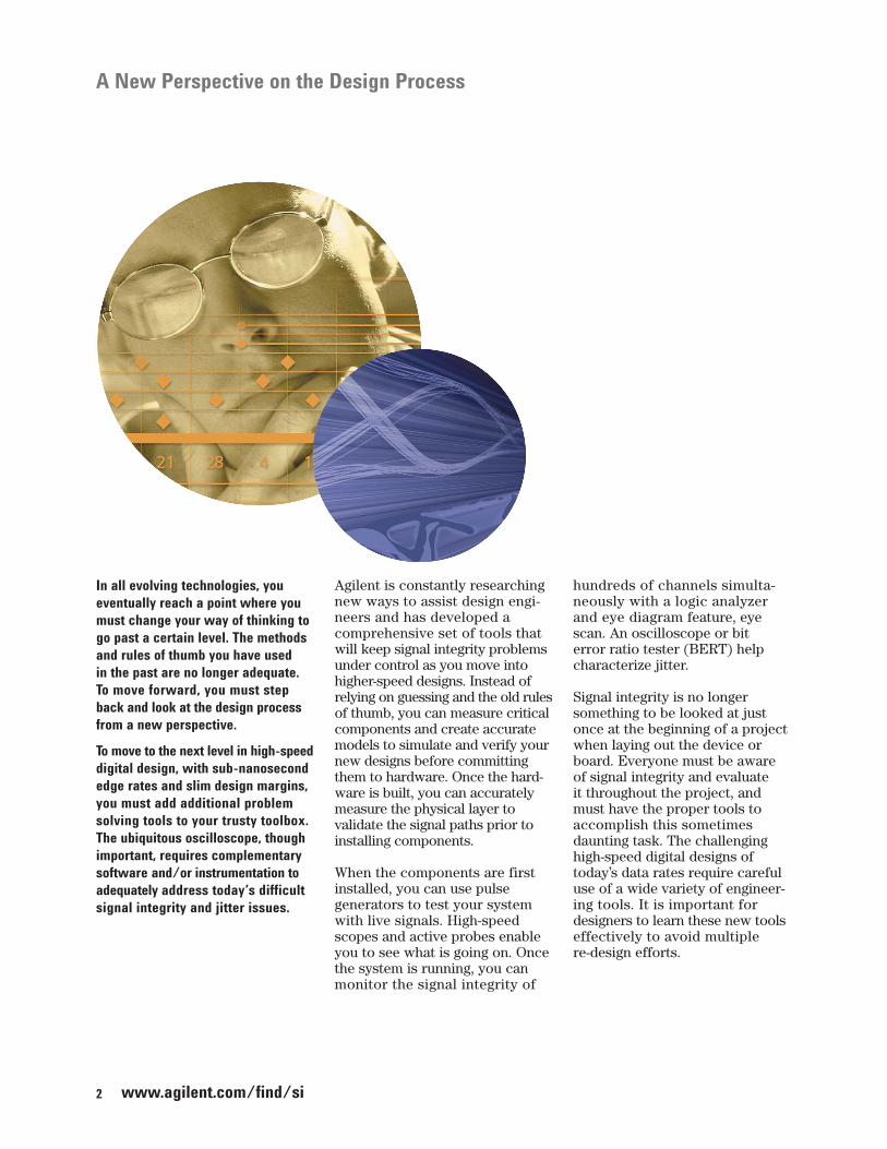
A New Perspective on the Design Process
Agilent is constantly researchingnew ways to assist design engi-neers and has developed acomprehensive set of tools thatwill keep signal integrity problemsunder control as you move intohigher-speed designs. Instead ofrelying on guessing and the old rulesof thumb, you can measure criticalcomponents and create accuratemodels to simulate and verify yournew designs before committingthem to hardware. Once the hard-ware is built, you can accuratelymeasure the physical layer tovalidate the signal paths prior toinstalling components.
When the components are firstinstalled, you can use pulsegenerators to test your systemwith live signals. High-speedscopes and active probes enableyou to see what is going on. Oncethe system is running, you canmonitor the signal integrity of
In all evolving technologies, youeventually reach a point where youmust change your way of thinking togo past a certain level. The methodsand rules of thumb you have used in the past are no longer adequate.To move forward, you must step back and look at the design processfrom a new perspective.
To move to the next level in high-speeddigital design, with sub-nanosecondedge rates and slim design margins,you must add additional problemsolving tools to your trusty toolbox.The ubiquitous oscilloscope, thoughimportant, requires complementarysoftware and/or instrumentation toadequately address today’s difficultsignal integrity and jitter issues.
hundreds of channels simulta-neously with a logic analyzerand eye diagram feature, eyescan. An oscilloscope or bit error ratio tester (BERT) helpcharacterize jitter.
Signal integrity is no longersomething to be looked at justonce at the beginning of a projectwhen laying out the device orboard. Everyone must be awareof signal integrity and evaluate it throughout the project, andmust have the proper tools toaccomplish this sometimesdaunting task. The challenginghigh-speed digital designs oftoday’s data rates require carefuluse of a wide variety of engineer-ing tools. It is important fordesigners to learn these new toolseffectively to avoid multiple re-design efforts.
www.agilent.com/find/si
www.agilent.com/find/jitter
DESIGN SIMULATION
Link to ModelDatabase
ADS
SPICE/IBIS
Devices & InterconnectCharacterization
Prototype Characterization& Validation
Bring-Up Test
System Integration& Functional Validation
DEVICE & BOARD
P H Y S I C A L L A Y E R L I N K L A Y E R
SYSTEMDESIGN SIMULATION DEVICE & BOARD SYSTEM
Passive Interconnect MeasurementsIMPEDANCE, CROSSTALK...
Device Characterization andModelling Services
Physical LayerTest System
(PLTS)
86100withTDR
PNASeriesVNA
Serial/Parallel BERT ProtocolAnalyzer
&Exerciser81133/4 Pulse Pattern Generator
16700 Series Logic System w/Eye Scan & Soft Touch Probes
86100 Infiniium DCA
54855 6 GHz Infiniium Oscilloscope
InfiniiMax Probing System
Active Live Signal MeasurementsVOLTAGE, JITTER, BER, TIMING, PACKETS...
3
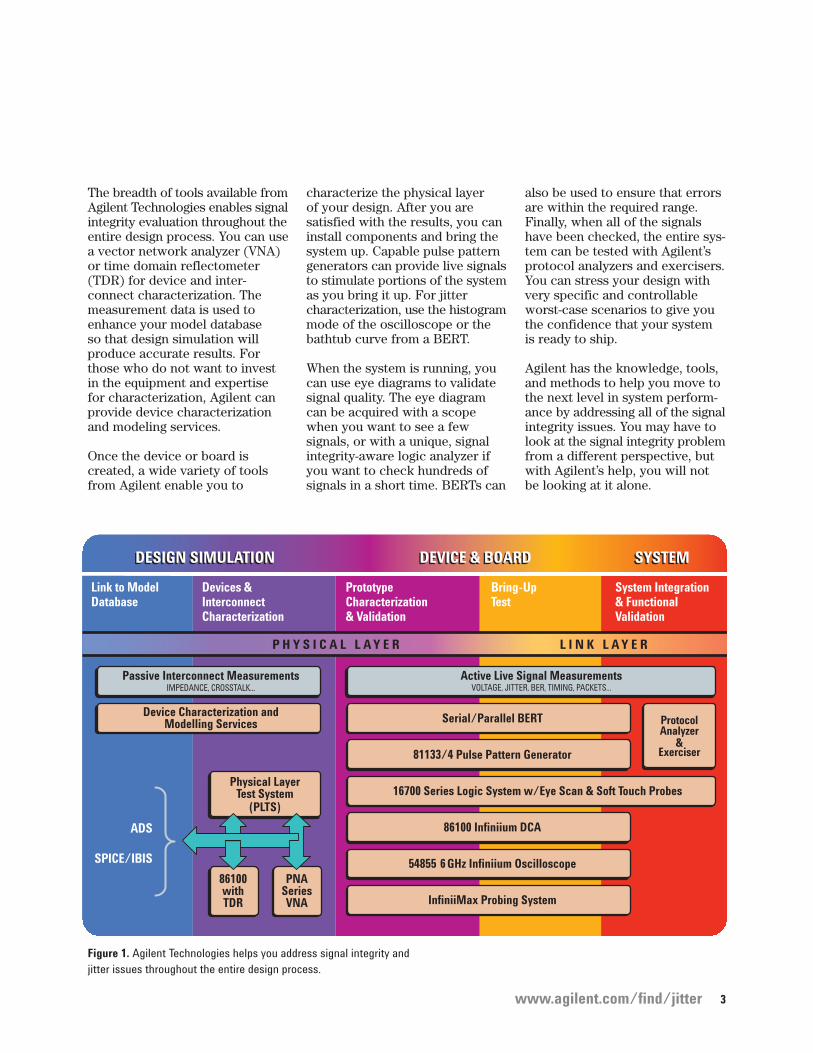
The breadth of tools available fromAgilent Technologies enables signalintegrity evaluation throughout theentire design process. You can usea vector network analyzer (VNA)or time domain reflectometer(TDR) for device and inter-connect characterization. Themeasurement data is used toenhance your model database so that design simulation willproduce accurate results. Forthose who do not want to investin the equipment and expertisefor characterization, Agilent canprovide device characterizationand modeling services.
Once the device or board iscreated, a wide variety of toolsfrom Agilent enable you to
characterize the physical layer of your design. After you aresatisfied with the results, you caninstall components and bring thesystem up. Capable pulse patterngenerators can provide live signalsto stimulate portions of the systemas you bring it up. For jittercharacterization, use the histogrammode of the oscilloscope or thebathtub curve from a BERT.
When the system is running, youcan use eye diagrams to validatesignal quality. The eye diagramcan be acquired with a scopewhen you want to see a fewsignals, or with a unique, signalintegrity-aware logic analyzer ifyou want to check hundreds ofsignals in a short time. BERTs can
also be used to ensure that errorsare within the required range. Finally, when all of the signalshave been checked, the entire sys-tem can be tested with Agilent’sprotocol analyzers and exercisers.You can stress your design withvery specific and controllableworst-case scenarios to give youthe confidence that your system is ready to ship.
Agilent has the knowledge, tools,and methods to help you move tothe next level in system perform-ance by addressing all of the signalintegrity issues. You may have tolook at the signal integrity problemfrom a different perspective, butwith Agilent’s help, you will notbe looking at it alone.
Figure 1. Agilent Technologies helps you address signal integrity andjitter issues throughout the entire design process.

4
Oscilloscopes and Probes
When you are developing evenfaster systems that have edge ratesless than 40 ps, you will need ascope with significant bandwidth.The 86100C Infiniium DCA-Jaccepts modules that provide upto 80-GHz of electrical bandwidth.A remote sampling head for the86100C allows the user to minimizebandwidth loss due to long cables.
Testing today’s high-speed serialbuses is simplified with applicationsoftware for the Infiniium 80000Series oscilloscopes. Perform masktesting and characterize serial datastreams that employ embeddedclocks and 8b/10b encoding.Verify compliance to standardssuch as PCI Express, Serial ATA,DVI, and Gigabit Ethernet.
Characterizing jitter is easy usingthe Infiniium 80000 Series real-time oscilloscope or 86100CInfiniium DCA-J with the optionaljitter analysis software thatinclude histogram, spectrum, andrandom/deterministic jitter(RJ/DJ) separation capabilities.
www.agilent.com/find/si
Figure 2. The Agilent 80000 Series Oscilloscopes and InfiniiMax IISeries probes deliver a high-performance 13 GHz end-to-endmeasurement system.
Figure 3. The Agilent 86100 DCA-J is a digital communicationsanalyzer, a wide-bandwidth oscilloscope, a jitter analyzer, and atime-domain reflectometer.
Prototype Characterization
Bring-Up Test
When you suspect a signalintegrity-related problem, the first instrument you grab is anoscilloscope. The scope is thebest instrument for finding outwhat a signal looks like. It willcontinue to be an important toolfor understanding signal integrityproblems, but it is only one ofmany tools that are now required.
You will need a scope that canaccurately measure sub 50 psedge rates. The Infiniium 80000Series provides up to 13 GHzbandwidth and an intuitiveWindows® interface that makes it easy to analyze signals and get the information you need. Itcan characterize critical signalparameters, such as setup andhold time violations, edge rates,overshoot, and jitter.
As an experienced scope user, youknow that your measurements areonly as good as your probingsystem. And as bandwidthincreases, it’s increasinglyimportant to ask the question: am I measuring my circuit or myscope probe? Nothing is morefrustrating than chasing down anapparent design problem, only tofind that it was caused by aninferior scope probe.
Together, the newest Infiniiumscopes and the innovativeInfiniiMax high-performanceprobing systems offer anend-to-end measurement systemwith unmatched performance,accuracy and connectivity.InfiniiMax II probes, with up to13 GHz bandwidth, can measuredifferential and single-endedsignals. Their flexibility supportseven the most demanding
mechanical accessrequirements withoutsacrificing performance.The result is measurementsyou can trust and betterinsight into circuit behavior.

www.agilent.com/find/jitter 5
Logic Analysis System
Hundreds of signal traces movingdata along wide data paths at high speeds can present quite achallenge to the high-speed digitaldesigner. The interaction of thesehundreds of signal lines keepssignal integrity in the forefront. Youmust validate the signal integrityof each signal path in order to befully confident of your design.
The typical method for validatingall of the signals is to use a 2- or4-channel scope and measure eye diagrams. This can take aconsiderable amount of time andis often deleted from the projectas many back-end tests fall victimto sliding schedules. The idealalternative to making hundreds ofeye-diagram measurements with ascope is a novel technology called“eye scan.”
With eye scan, you can have thesame eye-diagram capability in alogic analyzer that you have inyour scope, and cover up to 340channels at a time. Eye scan givesyou a rapid, comprehensiveoverview across hundreds ofsignals simultaneously. Eye scan isavailable in the Agilent 1680/1690Series standalone logic analyzersand the 16950A, 16760A, 16750Series, and 16740 Series logicanalyzer modules for the 16900Series logic analysis systems. Ifeye scan finds a bad signal andyou need more detail, you cantake a closer look by making atime-correlated measurementbetween the logic analyzer and anAgilent oscilloscope.
The Agilent 16760A provides a1.5-Gb/s state acquisition rate and128-M sample memory depth. Itcan acquire differential signalswith a probing system thatpresents only 0.7-pF capacitive
loading to preserve your system’ssignal integrity. It has an equivalentbandwidth of 2.33 GHz whenusing eye scan.
On your next project, use Agilent’sinnovative, time-saving eye scantechnology for a comprehensiveoverview of the system’s signalintegrity. Immediately spotproblems and identify theoffending signals. Use the timeyou gain to check out signalintegrity under all conditions.
Quality measurements start at theprobe tips. Agilent’s soft touchprobes meet the demand foraccuracy and reliability whileproviding connectorless contactwith your device. Available insingle-ended and differentialversions, the contact approachalso minimizes multi-layer board
Figure 4. View the eye diagrams of manychannels simultaneously with a logicanalyzer and spot sub-nanosecondproblems faster than conventional methods.
Figure 5. Agilent’s soft touch probescombine high-density, low loading anddifferential capability into a reliablespace-saving package.
Prototype Characterization
Bring-Up Test
System Integration & Functional Validation
layout issues. With less than0.7 pF capacitive loading, you can maintain tight timing marginswith the soft touch probeattached to your board.
6
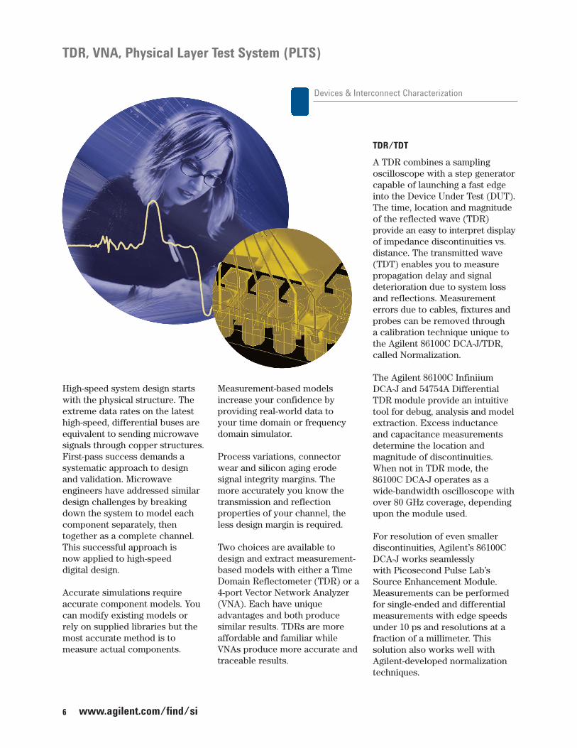
High-speed system design startswith the physical structure. Theextreme data rates on the latesthigh-speed, differential buses areequivalent to sending microwavesignals through copper structures.First-pass success demands asystematic approach to designand validation. Microwaveengineers have addressed similardesign challenges by breakingdown the system to model eachcomponent separately, thentogether as a complete channel.This successful approach is now applied to high-speed digital design.
Accurate simulations requireaccurate component models. Youcan modify existing models orrely on supplied libraries but themost accurate method is tomeasure actual components.
Measurement-based modelsincrease your confidence byproviding real-world data to your time domain or frequencydomain simulator.
Process variations, connectorwear and silicon aging erodesignal integrity margins. The more accurately you know thetransmission and reflectionproperties of your channel, theless design margin is required.
Two choices are available todesign and extract measurement-based models with either a TimeDomain Reflectometer (TDR) or a4-port Vector Network Analyzer(VNA). Each have uniqueadvantages and both producesimilar results. TDRs are moreaffordable and familiar whileVNAs produce more accurate andtraceable results.
TDR/TDT
A TDR combines a samplingoscilloscope with a step generatorcapable of launching a fast edgeinto the Device Under Test (DUT).The time, location and magnitudeof the reflected wave (TDR)provide an easy to interpret displayof impedance discontinuities vs.distance. The transmitted wave(TDT) enables you to measurepropagation delay and signaldeterioration due to system lossand reflections. Measurementerrors due to cables, fixtures andprobes can be removed through a calibration technique unique tothe Agilent 86100C DCA-J/TDR,called Normalization.
The Agilent 86100C InfiniiumDCA-J and 54754A DifferentialTDR module provide an intuitivetool for debug, analysis and modelextraction. Excess inductanceand capacitance measurementsdetermine the location andmagnitude of discontinuities.When not in TDR mode, the86100C DCA-J operates as awide-bandwidth oscilloscope withover 80 GHz coverage, dependingupon the module used.
For resolution of even smallerdiscontinuities, Agilent’s 86100CDCA-J works seamlessly with Picosecond Pulse Lab’sSource Enhancement Module.Measurements can be performedfor single-ended and differentialmeasurements with edge speedsunder 10 ps and resolutions at afraction of a millimeter. Thissolution also works well withAgilent-developed normalizationtechniques.
TDR, VNA, Physical Layer Test System (PLTS)
www.agilent.com/find/si
Devices & Interconnect Characterization
www.agilent.com/find/jitter 7
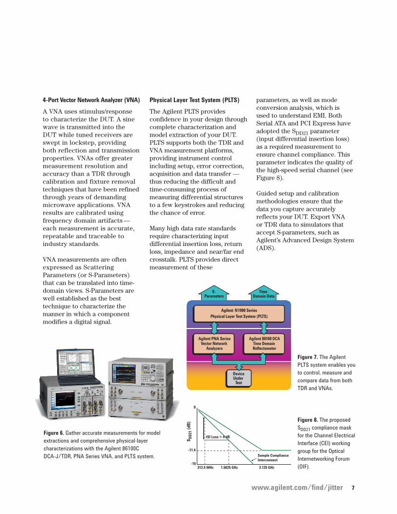
Figure 6. Gather accurate measurements for modelextractions and comprehensive physical-layercharacterizations with the Agilent 86100CDCA-J/TDR, PNA Series VNA, and PLTS system.
4-Port Vector Network Analyzer (VNA)
A VNA uses stimulus/response to characterize the DUT. A sinewave is transmitted into the DUT while tuned receivers areswept in lockstep, providingboth reflection and transmissionproperties. VNAs offer greatermeasurement resolution andaccuracy than a TDR throughcalibration and fixture removaltechniques that have been refinedthrough years of demandingmicrowave applications. VNAresults are calibrated usingfrequency domain artifacts — each measurement is accurate,repeatable and traceable toindustry standards.
VNA measurements are oftenexpressed as ScatteringParameters (or S-Parameters)that can be translated into time-domain views. S-Parameters arewell established as the besttechnique to characterize themanner in which a componentmodifies a digital signal.
Physical Layer Test System (PLTS)
The Agilent PLTS providesconfidence in your design throughcomplete characterization andmodel extraction of your DUT.PLTS supports both the TDR andVNA measurement platforms,providing instrument controlincluding setup, error correction,acquisition and data transfer —thus reducing the difficult andtime-consuming process ofmeasuring differential structuresto a few keystrokes and reducingthe chance of error.
Many high data rate standardsrequire characterizing inputdifferential insertion loss, returnloss, impedance and near/far endcrosstalk. PLTS provides directmeasurement of these
parameters, as well as modeconversion analysis, which isused to understand EMI. BothSerial ATA and PCI Express haveadopted the SDD21 parameter(input differential insertion loss)as a required measurement toensure channel compliance. Thisparameter indicates the quality ofthe high-speed serial channel (seeFigure 8).
Guided setup and calibrationmethodologies ensure that thedata you capture accuratelyreflects your DUT. Export VNA or TDR data to simulators thataccept S-parameters, such asAgilent’s Advanced Design System(ADS).
Time Domain Data
Agilent N 1900 SeriesPhysical Layer Test System (PLTS)
S-Parameters
DeviceUnder
Test
Agilent PNA SeriesVector Network
Analyzers
Agilent 86100 DCATime Domain Reflectometer
Figure 7. The AgilentPLTS system enables youto control, measure andcompare data from bothTDR and VNAs.
Sample Compliance Interconnect
S DD
21 (
dB)
ISI Loss > 4 dB
312.5 MHz 1.5625 GHz 3.125 GHz
0
-11.4
-15
Figure 8. The proposedSDD21 compliance maskfor the Channel ElectricalInterface (CEI) workinggroup for the OpticalInternetworking Forum(OIF).

8 www.agilent.com/find/si
While bringing a system up, it is often necessary to stimulate aportion of the system before theentire system is running. A pulse/pattern generator can provide the stimulus signals used by ascope to make eye diagrams. Thegenerator must also allow you tostress the system by adding control-lable jitter to the stimulus signal.
The 81134A pulse pattern generatoris a high-performance and easy-to-use pulse and data-pattern sourcefor characterizing the physicallayer as well as verifying and
validating high-speed clock sys-tems. The graphical user interfaceenables you to easily set up verycomplex signals. From generatingPRBS to adding jitter to yourclock or data, the 81134A givesyou the required signals.
With the capability of easilyuploading any data pattern up to12 Mbit, a real life data pattern is easily created.
The fast rise times, low jitter, andfull parameter flexibility providejust the signal you need, especiallyin high-speed systems wheretiming is critical. Performance canbe evaluated with eye-diagrammeasurements with PRBS from 2 5-1 to 231 -1. The delay control
Pulse Pattern Generator
Figure 9. The Agilent 81133/4 pulse pattern generator enables the precisecharacterization of devices and minimizes the influence of jitter injection by thesource with superior signal performance up to 3.35 GHz.
Prototype Characterization
Bring-Up Test
input allows you to add jitter tothe clock or data signals. The eyecan be distorted with the variablecrossover function.
Other features include LVDS levelsand a remote graphical user inter-face and SCPI commands forremote handling and programming.
www.agilent.com/find/jitter
Link to Model Database
Devices and Interconnect Characterization
Prototype Characterization
Bring-Up Test
System Integration & Functional Validation
9
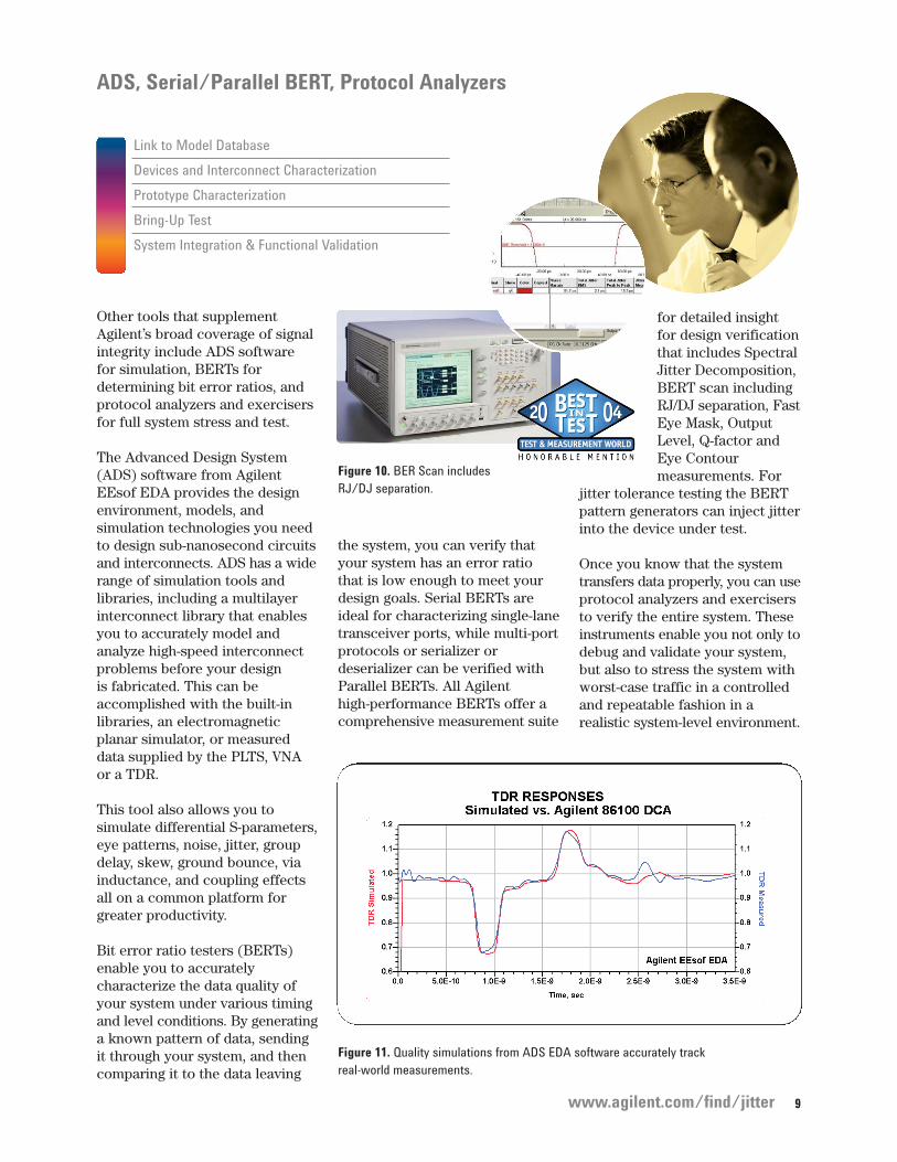
ADS, Serial/Parallel BERT, Protocol Analyzers
Other tools that supplementAgilent’s broad coverage of signalintegrity include ADS software for simulation, BERTs fordetermining bit error ratios, andprotocol analyzers and exercisersfor full system stress and test.
The Advanced Design System(ADS) software from AgilentEEsof EDA provides the designenvironment, models, andsimulation technologies you needto design sub-nanosecond circuitsand interconnects. ADS has a widerange of simulation tools andlibraries, including a multilayerinterconnect library that enablesyou to accurately model andanalyze high-speed interconnectproblems before your design is fabricated. This can beaccomplished with the built-inlibraries, an electromagneticplanar simulator, or measureddata supplied by the PLTS, VNAor a TDR.
This tool also allows you tosimulate differential S-parameters,eye patterns, noise, jitter, groupdelay, skew, ground bounce, viainductance, and coupling effectsall on a common platform forgreater productivity.
Bit error ratio testers (BERTs)enable you to accuratelycharacterize the data quality ofyour system under various timingand level conditions. By generatinga known pattern of data, sendingit through your system, and thencomparing it to the data leaving
the system, you can verify thatyour system has an error ratiothat is low enough to meet yourdesign goals. Serial BERTs areideal for characterizing single-lanetransceiver ports, while multi-portprotocols or serializer ordeserializer can be verified withParallel BERTs. All Agilenthigh-performance BERTs offer acomprehensive measurement suite
for detailed insightfor design verificationthat includes SpectralJitter Decomposition,BERT scan includingRJ/DJ separation, FastEye Mask, OutputLevel, Q-factor andEye Contourmeasurements. For
jitter tolerance testing the BERTpattern generators can inject jitterinto the device under test.
Once you know that the systemtransfers data properly, you can useprotocol analyzers and exercisersto verify the entire system. Theseinstruments enable you not only todebug and validate your system,but also to stress the system withworst-case traffic in a controlledand repeatable fashion in arealistic system-level environment.
Figure 11. Quality simulations from ADS EDA software accurately trackreal-world measurements.
Figure 10. BER Scan includesRJ/DJ separation.
10
Not only does Agilent provide youwith the tools and training neces-sary to make the measurementsyou need, Agilent also provides a signal integrity measurementservice that gives you the signalintegrity data you need. Thisservice can provide impedancecharacterization of high-speedinterconnects and accurate modelsfor your simulations. Crosstalk,reflected and transmitted lossescan be measured. Lossy trans-mission line models can be derivedfrom measurements that enabledesigners to accurately predictnot only interconnect-inducedringing and reflections, but alsoamplitude loss, jitter, eye-diagramdegradation, and crosstalk.
A qualified Agilent engineer, usingthe appropriate equipment, canmake the following measurementsat your site or in an Agilent lab:
• High-speed interconnect imped-ance measurements
• SPICE model generation andvalidation from actual measure-ments of printed and flexiblecircuit boards, cables, cableassemblies, and connectors
• Frequency-dependent lossmodeling, insertion, and return-loss analysis
This is a complete service thatalleviates the need for you topurchase the necessary equipmentand software and to acquire theexpertise to make such measure-ments. This requires you to provideonly the components, prototypes,or test fixtures to be used in themeasurement.
For more information aboutAgilent’s professional engineeringservices (available in NorthAmerica only), log ontowww.agilent.com/find/si-services.
Device Characterization and Modeling Services(available in North America only)
Link to Model Database
Devices and Interconnect Characterization
www.agilent.com/find/si
11www.agilent.com/find/jitter
Mode
l Extr
actio
n & Veri
ficati
on
Electro
nic Des
ign
Enclosu
re/M
echan
ical D
esign
Mode
ling/
Simulat
ion Tools
Jitter C
haracte
rizati
on
Operat
ional Chara
cteriz
ation/Sim
ulation
Probing P
roducts
Fixtures
/Fixturin
g
SI Edu
catio
n & Tr
aining
Signal Integrity Channel Partners
Related Literature
86100C Agilent Infiniium DCA-J Color Brochure 5988-5235EN
Infiniium 80000 Series Oscilloscopes & Data Sheet 5989-1487ENInfiniiMax II Probes
16900 Series Logic Analysis Systems Color Brochure 5989-0420EN
Soft Touch Connectorless Photo Card 5988-8128EN Logic Analyzer Probes
81133 and 81134 3.35 GHz Data Sheet 5988-5549ENPulse Pattern Generators
Serial/Parallel BERTs Color Brochure 5988-9514EN
Physical Layer Test Systems (PLTS) Product Overview 5988-5288EN
EEsof EDA Color Brochure 5988-3326EN
Jitter Solutions for Telecom, Enterprise, and Digital Designs Color Brochure 5988-9592EN
The Many Faces of Digital Jitter Color Poster 5989-0830EN
Partner for Success
Agilent Channel Partners areindustry experts with world-renowned expertise in SignalIntegrity. Their experiencecombined with Agilent measure-ment tools can enable you toaddress both your technical andbusiness constraints, providingwhat is needed to keep your high-speed digital products onthe competitive “leading edge”.
See table on the right for more detail about Agilent’sChannel Partners.
Channel Partner Offering(s) / Capabilities
Bogatin Enterprises, LLC Xwww.bethesignal.com
Cascade Microtech, Inc. Xwww.cascademicrotech.com
FuturePlus Systems X Xwww.futureplus.com
GigaTest Labs X X X X Xwww.gigatest.com
Inter-Continental Microwave Xwww.icmicrowave.com
MicroTest Xwww.microtst.org
Northeast Systems Associates X X X X X Xwww.nesa.com
Agilent Technologies’ Test andMeasurement Support, Services, andAssistanceAgilent Technologies aims to maximize thevalue you receive, while minimizing yourrisk and problems. We strive to ensure thatyou get the test and measurementcapabilities you paid for and obtain thesupport you need. Our extensive supportresources and services can help youchoose the right Agilent products for yourapplications and apply them successfully.Every instrument and system we sell has aglobal warranty. Two concepts underlieAgilent’s overall support policy: "OurPromise" and "Your Advantage."
Our PromiseOur Promise means your Agilent test andmeasurement equipment will meet itsadvertised performance and functionality.When you are choosing new equipment,we will help you with product information,including realistic performancespecifications and practical recommendations fromexperienced test engineers. When youreceive your new Agilent equipment, wecan help verify that it works properly andhelp with initial product operation.
Your AdvantageYour Advantage means that Agilent offersa wide range of additional expert test andmeasurement services, which you canpurchase according to your uniquetechnical and business needs. Solveproblems efficiently and gain a competitiveedge by contracting with us for calibration,extra-cost upgrades, out-of-warrantyrepairs, and on-site education and training,as well as design, system integration,project management, and otherprofessional engineering services.Experienced Agilent engineers andtechnicians worldwide can help youmaximize your productivity, optimize thereturn on investment of your Agilentinstruments and systems, and obtaindependable measurement accuracy for thelife of those products.
For more information on Agilent Technologies’products, applications or services, pleasecontact your local Agilent office. The completelist is available at:
www.agilent.com/find/contactus
Phone or FaxUnited States:(tel) 800 829 4444(fax) 800 829 4433
Canada:(tel) 877 894 4414(fax) 800 746 4866
China:(tel) 800 810 0189(fax) 800 820 2816
Europe:(tel) 31 20 547 2111
Japan:(tel) (81) 426 56 7832(fax) (81) 426 56 7840
Korea:(tel) (080) 769 0800(fax) (080)769 0900
Latin America:(tel) (305) 269 7500
Taiwan:(tel) 0800 047 866 (fax) 0800 286 331
Other Asia Pacific Countries:(tel) (65) 6375 8100 (fax) (65) 6755 0042Email: [email protected] revised: 05/27/05
Product specifications and descriptions in thisdocument subject to change without notice.
© Agilent Technologies, Inc. 2005Printed in USA August 29, 20055988-5405EN
www.agilent.com
www.agilent.com/find/siApplication Resources for Signal Integrity
www.agilent.com/find/jitterAgilent Jitter Solutions
www.agilent.com/find/sigintSignal Integrity Series of eSeminars
www.agilent.com/find/emailupdatesGet the latest information on the productsand applications you select.
www.agilent.com/find/agilentdirectQuickly choose and use your testequipment solutions with confidence.
Agilent Email Updates
Agilent Direct