Final Report on Microwave Power Transmission Using … · Final Report on . Microwave Power...
24
Final Report on Microwave Power Transmission Using Electromagnetic Coupling of Open-Ring Resonators Name of contractor The University of Tokushima Contract number FA2386-11-1-40084 Report period From June 28, 2011 to June 27, 2012 Author Yasuo Ohno(Professor) Institute of Technology and Science, The University of Tokushima 2-1 Minami-Josanjima, Tokushima 770-8506, Japan E-mail: [email protected] Abstract Experimental results on 60GHz band signal transmission through ECOR (Electromagnetic Coupling of Open-Ring Resonators) are shown. Through 200μm sapphire substrate, 60-70GHz band signal are transmitted with 58.9% transmission efficiency and 7.4GHz bandwidth. However, the transmission band was shifted about 10GHz higher frequency. The reason is under investigation. ECOR technology is extended to lower frequencies for non-contact power transmission. The technology will benefit to power connectors for equipment modules where the problems caused by humidity and mechanical failure will be eliminated. A new diode structure for RF signal rectification, loss mechanism in rectenna circuits and the effect of wetting to ECOR transmission will be presented. This report consists of the following four sections. 1. 60 GHz Wireless Interconnection Using ECOR 2. T-shaped Anode GaN Schottky Barrier Diode for Microwave Power Rectification 3. Analysis of Loss Mechanism in Rectenna Circuit 4. Effects of Wetting to Wireless Power Transmission by Open-Ring Resonators Coupling 1
Transcript of Final Report on Microwave Power Transmission Using … · Final Report on . Microwave Power...

Final Report on
Microwave Power Transmission Using Electromagnetic Coupling of
Open-Ring Resonators
Name of contractor The University of Tokushima Contract number FA2386-11-1-40084 Report period From June 28, 2011 to June 27, 2012 Author Yasuo Ohno(Professor)
Institute of Technology and Science, The University of Tokushima 2-1 Minami-Josanjima, Tokushima 770-8506, Japan E-mail: [email protected]
Abstract
Experimental results on 60GHz band signal transmission through ECOR (Electromagnetic Coupling of
Open-Ring Resonators) are shown. Through 200μm sapphire substrate, 60-70GHz band signal are transmitted
with 58.9% transmission efficiency and 7.4GHz bandwidth. However, the transmission band was shifted about
10GHz higher frequency. The reason is under investigation.
ECOR technology is extended to lower frequencies for non-contact power transmission. The technology will
benefit to power connectors for equipment modules where the problems caused by humidity and mechanical
failure will be eliminated. A new diode structure for RF signal rectification, loss mechanism in rectenna circuits
and the effect of wetting to ECOR transmission will be presented.
This report consists of the following four sections.
1. 60 GHz Wireless Interconnection Using ECOR
2. T-shaped Anode GaN Schottky Barrier Diode for Microwave Power Rectification
3. Analysis of Loss Mechanism in Rectenna Circuit
4. Effects of Wetting to Wireless Power Transmission by Open-Ring Resonators Coupling
1

Report Documentation Page Form ApprovedOMB No. 0704-0188
Public reporting burden for the collection of information is estimated to average 1 hour per response, including the time for reviewing instructions, searching existing data sources, gathering andmaintaining the data needed, and completing and reviewing the collection of information. Send comments regarding this burden estimate or any other aspect of this collection of information,including suggestions for reducing this burden, to Washington Headquarters Services, Directorate for Information Operations and Reports, 1215 Jefferson Davis Highway, Suite 1204, ArlingtonVA 22202-4302. Respondents should be aware that notwithstanding any other provision of law, no person shall be subject to a penalty for failing to comply with a collection of information if itdoes not display a currently valid OMB control number.
1. REPORT DATE 01 NOV 2012
2. REPORT TYPE Final
3. DATES COVERED 28-06-2011 to 27-06-2012
4. TITLE AND SUBTITLE Microwave Power Transmission Using Electromagnetic Coupling ofOpen-Ring Resonators
5a. CONTRACT NUMBER FA23861114084
5b. GRANT NUMBER
5c. PROGRAM ELEMENT NUMBER
6. AUTHOR(S) Yasuo Ohno
5d. PROJECT NUMBER
5e. TASK NUMBER
5f. WORK UNIT NUMBER
7. PERFORMING ORGANIZATION NAME(S) AND ADDRESS(ES) The University of Tokushima,2-1 Minami-Josanjima-cho,Tokushima-shi 770-8506,Japan,JP,770-8506
8. PERFORMING ORGANIZATIONREPORT NUMBER N/A
9. SPONSORING/MONITORING AGENCY NAME(S) AND ADDRESS(ES) AOARD, UNIT 45002, APO, AP, 96338-5002
10. SPONSOR/MONITOR’S ACRONYM(S) AOARD
11. SPONSOR/MONITOR’S REPORT NUMBER(S) AOARD-114084
12. DISTRIBUTION/AVAILABILITY STATEMENT Approved for public release; distribution unlimited
13. SUPPLEMENTARY NOTES
14. ABSTRACT Experimental results on 60GHz band signal transmission through ECOR (Electromagnetic Coupling ofOpen-Ring Resonators) are shown. Through 200μm sapphire substrate, 60-70GHz band signal aretransmitted with 58.9% transmission efficiency and 7.4GHz bandwidth. However, the transmission bandwas shifted about 10GHz higher frequency. The reason is under investigation. ECOR technology isextended to lower frequencies for non-contact power transmission. The technology will benefit to powerconnectors for equipment modules where the problems caused by humidity and mechanical failure will beeliminated. A new diode structure for RF signal rectification, loss mechanism in rectenna circuits and theeffect of wetting to ECOR transmission will be presented. This report consists of the following foursections: 60 GHz Wireless Interconnection Using ECOR, T-shaped Anode GaN Schottky Barrier Diode forMicrowave Power Rectification, Analysis of Loss Mechanism in Rectenna Circuit, Effects of Wetting toWireless Power Transmission by Open-Ring Resonators Coupling
15. SUBJECT TERMS microwave devices and circuits, RF, Microwave Engineering
16. SECURITY CLASSIFICATION OF: 17. LIMITATION OF ABSTRACT Same as
Report (SAR)
18. NUMBEROF PAGES
22
19a. NAME OFRESPONSIBLE PERSON
a. REPORT unclassified
b. ABSTRACT unclassified
c. THIS PAGE unclassified

Standard Form 298 (Rev. 8-98) Prescribed by ANSI Std Z39-18

1 60 GHz Wireless Interconnection Using ECOR[1]
1.1 ECOR
Several on-chip wireless interconnects have been proposed, such as antenna-type, capacitive
coupling and inductive coupling. They are convenient to distribute signals on and out of chips, but
the energy efficiency is too low to use the received signal without amplification. So, we proposed
electromagnetic coupling of open-ring resonators (ECOR) to realize low-cost millimeter wave
transceivers as shown in Fig.1.1 [2].
Resonator coupling is short distance but efficient
transmission technology, so it has been used for meter-range
wireless power transmission, such as WiTricity [3].
As device miniaturization has proceeded, CMOS can
generate 60GHz signals, but the handling power is reduced. On
the other hand, AlGaN/GaN HFETs can generate high power
at millimeter wave range. To combine these technologies,
conventional mechanical interconnection is not suited due to
signal degradation and high assembly cost. So, we have ECOR
to realize low-cost millimeter wave transceivers as shown in
Fig.1.2 [4].
In the project last year we have designed ECOR for 60GHz
signal transmission through sapphire wafers. We made gold
wiring patterns of open-rings, CPW transmission lines and
probe pads on sapphire and measured the transmission
characteristics. 60 GHz range signals are transmitted through
200 m thick sapphire substrate with 2.3dB insertion loss
(58.9% transmission) and 7.4GHz bandwidth, but the
transmission band are shifted about 10GHz higher frequencies.
Fig.1.1. ECOR structure for HFSS simulation. All the substrates are assumed to be sapphire with isotropic dielectric constant of 10.
1.2 Interconnect Structure
onator with circular shape to
pr
Open-ring resonator is a /2 res
event radiation loss (Fig.1.3) [5]. When two resonators are
placed closely, they couple electromagnetically and exchange
energy wirelessly. Then, the resonant frequency splits and a
band pass filter (BPF) is formed. The resonance occurs only
within distance less than the wavelength. For 60GHz, it is
(a) (b) Fig. 1.3. (a) simple λ/2 resonator whichworks as antenna, (b) open-ringresonator
λ/2
λ/2
silicon LSI(base band)
AlGaN/GaN HFET on sapphire
(modulation, amplify)
antenna on plastic plate
wireless interconnection silicon LSI
(base band)
AlGaN/GaN HFET on sapphire
(modulation, amplify)
antenna on plastic plate
wireless interconnection
Fig.1.2. Schematic model of millimeter wave system using ECOR (Electromagnetic coupling of open-ring resonator).
2
50
60
70
80
90
0 50 100 150
PORT ANGLE(deg )
FREQ
UENC
Y(G
Hz)
-3dB
peak
-3dB
-30
-25
-20
-15
-10
-5
0
50 55 60 65 70 75
FREQUENCY (GHz)
S11,
S21 (
dB
)
S21_GOLD
S11_GOLD
S21_PEC
S11_PEC
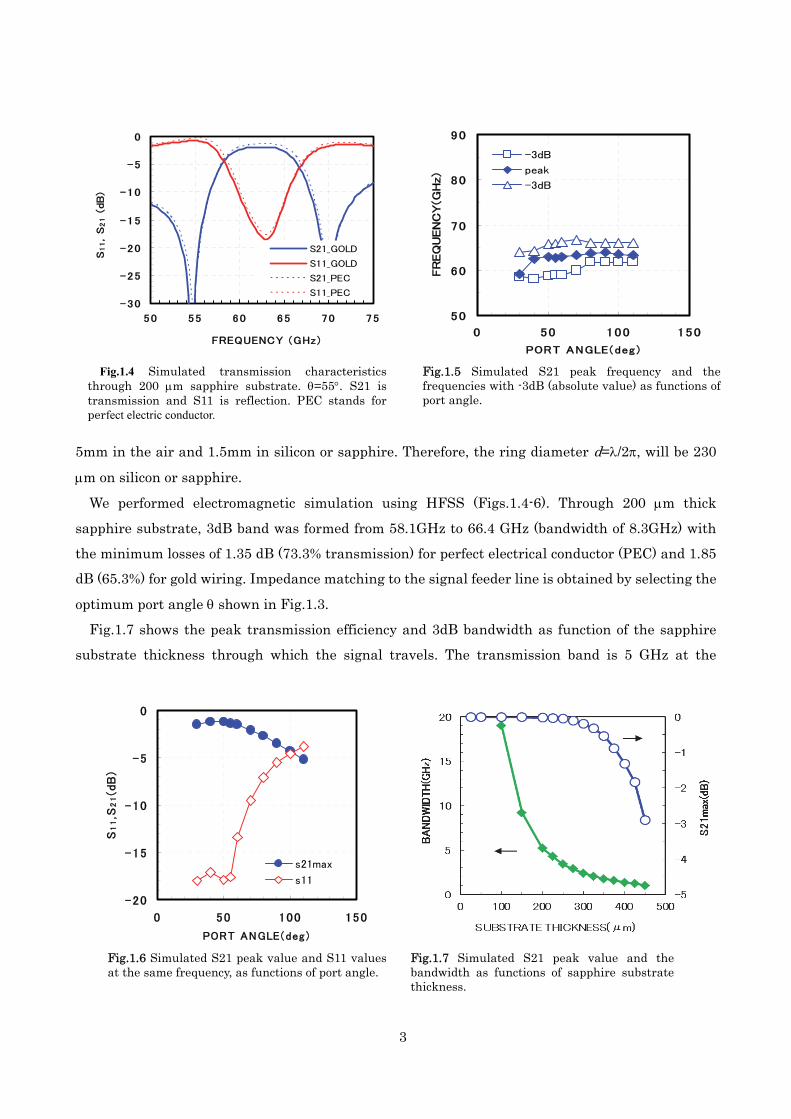
Fig.1.5 Simulated S21 peak frequency and the frequencies with -3dB (absolute value) as functions of port angle.
Fig.1.4 Simulated transmission characteristicsthrough 200 m sapphire substrate. =55. S21 istransmission and S11 is reflection. PEC stands forperfect electric conductor.
5mm in the air and 1.5mm in silicon or sapphire. Therefore, the ring diameter d=/2, will be 230
m on silicon or sapphire.
We performed electromagnetic simulation using HFSS (Figs.1.4-6). Through 200 m thick
sapphire substrate, 3dB band was formed from 58.1GHz to 66.4 GHz (bandwidth of 8.3GHz) with
the minimum losses of 1.35 dB (73.3% transmission) for perfect electrical conductor (PEC) and 1.85
dB (65.3%) for gold wiring. Impedance matching to the signal feeder line is obtained by selecting the
optimum port angle shown in Fig.1.3.
Fig.1.7 shows the peak transmission efficiency and 3dB bandwidth as function of the sapphire
substrate thickness through which the signal travels. The transmission band is 5 GHz at the
-20
-15
-10
-5
0
0 50 100 150
PORT ANGLE(deg )
S1
1,S
21(d
B)
s21max
s11
Fig.1.6 Simulated S21 peak value and S11 values at the same frequency, as functions of port angle.
Fig.1.7 Simulated S21 peak value and the bandwidth as functions of sapphire substrate thickness.
3

thickness of 200 m and the band exists up to 400 m.
1.3 Experiments
Based on the HFSS simulation, mask patterns are designed (Fig.1.8). The ring outer diameter is
335 m and the inner diameter is 145 m. 50 coplanar lines are connected to the rings for signal
input and output.
The ring and lines are made on c-plane sapphire substrate with the thickness of 200 m.
Conventional photo lithography technology and electrolytic plating of gold are used to make the
sample chips. The plated sample chips are overlapped, aligned and bonded with electron wax for the
measurement. The measurement was carried out using Agilent E8361A and N5260A with the
sample structure shown in Fig. 1.9.
The maximum transmission is obtained with the port angle of 80 and 55 as -2.3dB (58.9%)
(Fig.1.10, 1.11, 1.12). From simulation, the losses are estimated as 0.5dB by conductor and 1.35 dB
by radiation, maybe, by parallel plate mode propagating between the two metal planes. The
obtained loss values are not so bad for the first experiment.
Fig.1.8 Open-ring resonator patterns for s-parameter measurement. Patterns for the two layers are shown. In the actual measurement, the rings are aligned to overlap. The ring outer diameter is 335μm.
metal
Fig.1.9 Schematic diagram of the measurement set up.
sapphire
sapphire
sapphire
probe ring
probe ring
metal stage
-15
-10
-5
0
60 65 70 75 80 85
FREQUENCY(GHz)
S2
1(d
B)
θ= 55
θ= 80
Fig.1.10 Measured S21 for the rings with port angles of 55 and 80.
4

50
60
70
80
90
0 50 100 150
PORT ANGLE(deg)
FR
EQ
UE
NC
Y(G
Hz)
- 20
-15
-10
-5
0
0 50 100 150
PORT ANGLE(deg)
S1
1,S
21(d
B)
-3dB smax
fpeak S11
For 80 port angle, bandwidth defined by -3dB frequencies from the maximum S21 is obtained as
7.4GHz (68.175.5GHz). The band is shifted about 10 GHz higher than simulated frequencies. The
reason is not clear, but tuning will not be difficult for practical applications.
1.4 Conclusion
ECOR demonstrated 58.9% transmission efficiency and 7.4GHz bandwidth at 70GHz range for
the wireless transmission through 200m sapphire substrate.
ECOR has already been confirmed to works on high resistivity Si substrate (> 1 kcm) [6], and its
alignment tolerance is so wide as around a half the ring diameter [7]. In addition, ECOR is easy to
fabricate on any kind of material. It will contribute to low cost assembly and heterogeneous
integration of millimeter wave devices.
Fig.1.11 Measured S21 peak and the frequencies -3dB from the peak S21 value.
-3dB S22
Fig.1.12 Measured S21 peak value and the S11 values at the same frequency.
5

2 T-shaped Anode GaN Schottky Barrier Diode for Microwave Power
Rectification[8]
2.1 Introduction
Rectifying diode is a key device for rectenna circuit in microwave power transmission system. For high RF/DC
conversion efficiency, the reduction of ON-resistance (RON) and OFF-capacitance (COFF) is essential. For power
rectification, the voltage applicable to the diodes should be as high as possible. From these requirements, wide
bandgap semiconductors are expected to be used due to their high breakdown field and high electron mobility.
Breakdown field EC of GaN is 330V/m, which is about 10 times higher than that of silicon and GaAs. The
electron drift mobility 0 at low doping level is about 1500cm2/Vs, which is higher than that of silicon.
For actual diode design, several structure parameters should be considered, such as diode size and the doping
concentrations . The anode structure of our previous device is shown in Fig.2.1 (a), where the breakdown voltage
is assumed as 100V, so 1017cm-3 donor concentration and 1μm active layer thickness were selected [9,10,11]. Field
plate was used at the anode edge utilizing the alignment margin on Ni/Au layer for gold plating. The field plate
showed the breakdown voltage increase from
93V to 108V, but also the depletion capacitance
was increased about 25% in the zero voltage
capacitance. In this chapter, we will show a diode
with a new anode structure together with the
improved epi-layer design so that the OFF
capacitance and ON resistance will be reduced.
Au
2.2 GaN Schottky barrier diodes
Since there is no diffusion capacitance at
injection condition, Schottky barrier diodes
(SBD) are used for high frequency applications.
From simple one-dimensional calculation,
electrical characteristics of Schottky barrier diode
is obtained. Assuming S for anode area, t for
active layer thickness, ND for donor concentration
in the active layer and for electron drift
mobility, the diode ON resistance is written as,
DON NSq
tR
, (2.1)
where q is the unit charge. Also, the OFF
(a) (b) Fig.2.1 Schematic cross section of GaN SBD. (a)
Previous diode with field plate, (b) T-shapedanode diode.
Ni/A
Substrate
n-GaN
n+-GaN
Substrate
n+-GaN
SiO2
n-GaN
active layerND=1x1017cm-3
t=1.0μm
access layern+GaN
10mΩcm, t≈4μm
c-plane sapphire
3x1017cm-3,0.3μ
access layer n+GaN
10mΩcm, t≈4μm
c-plane sapphire
3x1017cm-3
0.4μm
access layern+GaN
10mΩcm, t≈4μm
c-plane sapphire
1x1017cm-3,0.1μ
(A) (B) (C)Fig.2.2 Epitaxial layer for the experiments. The sheetresistance of the access layer is about 25Ω.
6

capacitance under full depletion condition is given as,
tS
C SOFF
. (2.2)
Under these conditions, the bias voltage applied to the diode VMAX is qNDt2/2εS where εS is the dielectric
constant of the semiconductor. The field strength at the depletion edge is qNDt/εS and this value is EC at the
maximum voltage condition. Using these relations, the optimum epi-layer structure is given as,
C
MAX
EV
t2
, (2.3)
MAX
CSD qV
EN
2
2
. (2.4)
Using these relations, the time constant defined by the product of RON and COFF is given as,
2
2
C
MAXOFFON
E
VCR
. (2.5)
Thus, wide bandgap semiconductors are suited for microwave rectifying application due to their high
breakdown field.
2.3 T-shaped Anode Diode Structure
The device structure with T-shaped anode is shown in Fig. 2.1 (b). Fabrication process begins with the n-GaN
layer etching to expose n+-GaN layer by inductively coupled plasma (ICP) etching. Next, n+-GaN layer is etched
down to sapphire substrate for the isolation of bonding pads. Lift-off process is used for cathode Ohmic electrode
with Ti/Al/Ni (50/200/50nm) and Ni/Au(10/40nm) successively. Annealing is carried out at 850°C for 1 minute in
N2 ambient.
Next, anode electrode opening is formed in photo-resist with the thickness of 2m. Then, thin Ni/Au
(10nm/10nm) layer is deposited over the whole wafer by sputtering. This layer will be used for electrode layer in
Fig.2.3 Impurity concentration obtained from1MHz C-V measurement on 100μm diameterdiodes.
0 0.2 0.4 0.6 Distance(μm)
(C)
1018
1017
1016
Con
cent
ratio
n(c
(B)
(A)
Air Bridge Trench Isolation
anode pad
cathode pad
cathode pad
50μ
m
Fig.2.4 Photograph of one finger diode for s-parameter measurement.
7

gold electrolytic plating. The layer should be thin enough for the removal with the underlying photo-resist after
the plating. Next, thick photo-resist pattern is formed for gold plating. The gold plating layer also forms air-bridge
wiring between the anode electrodes and the bonding pads.
As discussed before, epi-layer design is important for low resistance and low capacitance. Since the peak to
peak voltage of diode is about 4 times of the input signal amplitude, 100V peak to peak voltage corresponds to
25W input signal on 50 Ω line. The power value is large enough for the battery charging of small mobile
equipment. So, we increased the donor concentration even with the decrease of breakdown voltage. Three
epitaxial layers are prepared as shown in Fig.2.2. We call the diodes with the epi-structures as diodes (A), (B) and
(C) in this paper. Fig. 2.3 shows the donor profile by 1 MHz C-V measurement on 100μm diameter circular
diodes.
1.E-07
1.E-06
1.E-05
1.E-04
1.E-03
1.E-02
1.E-01
1.E+00
-100 -80 -60 -40 -20 0BIAS(V)
CURR
ENT(
A)
(A)over100V
(B) 55V (C) 50V
0
50
100
0 1 2 3 4BIAS(V)
CURR
ENT(
mA)
(A)
(B)(C)
Fig.2.6 DC I-V characteristics in reverse direction.Fig.2.5 DC I-V characteristics.
-1
-0.5
-1 -0.5 0 0.5 1
1.17V
1.02V 0V
0
0.5
1
1.31V
3.0V
-10V
Fig. 2.7 S-parameters of diode (C) for differentbias voltage. Frequency range is from 10MHz to10 GHz and the dot indicate data at 2.45GHz.
COFF(v
RON
anode
cathod
LP
1exp
kTqVII S
Fig. 2.8 Circuit model of the diodes estimated from s-parameter measurement.
8

0
0.05
0.1
0.15
0.2
0 1 2 3 4BIAS(V)
COND
UCTA
NCE(
S)
(A)
(C)
(B)
0
0.1
0.2
0.3
-15 -10 -5 0
BIAS(V)
CAPA
CITA
NCE(
pF)
(C)(B)
(A)
Fig.2.9 Conductance obtained froms-parameter measurement at 2.45GHz(lines) and that obtained from DC I-V characteristics shown in Fig. 5 (marks).
Fig.2.10 Capacitance obtained froms-parameter measurement at 2.45GHz.
Table 2.1 Summary of the diode characteristics.Figure 2.4 shows the diode pattern for
s-parameter measurement of one-finger diode.
The finger size is 50μm long and 2μm wide.
The pads for probing are separated by deep
trench isolation down to sapphire substrate.
(B) (C) Device Ref[7] * (A)
2.4 Electrical Performance
Figure 2.5 shows DC I-V characteristics of
one-finger diodes. Turn on voltage defined at
1mA is 0.86V for diode (A) while it is around
1.15V for diodes (B) and (C), respectively. The
reason of the difference is not clear. Surface
condition may be different. Figure 2.6 shows
I-V characteristics in reverse direction. The breakdown voltage is 55V for diode (B) and 50V for diode (C). Due to
our equipment limitation, diode (A) did not show breakdown up to 100V.
S-parameters were measured using Agilent E8364B network analyzer with a source monitor unit Agilent
E5263A. Measurement is carried out from 10MHz to 10GHz changing bias voltage. Measured data on diode (C)
are shown in Fig. 2.7. Trajectories similar to typical RC series connection are appeared in reverse bias conditions
including zero bias. As the forward bias voltage increases, conductance parallel to the capacitance appears and
finally it shrinks to a pure low resistor circuit. For high forward bias condition, a small inductance around 50pH
was appeared. From these, we estimate the diode can be modeled by the components as shown in Fig. 2.8.
Figure 2.9 shows conductance obtained from s-parameters at 2.45GHz. Conductance calculated from DC I-V
characteristics is also shown. The difference between 2.45GHz and DC may come from the lack of cable
resistance calibration in DC measurement.
ND (cm-3) 1x10¹⁷ 1x10¹⁷ 1x10¹⁷
+3x10¹⁷ 3x10¹⁷
RON 16.4 26.3 8.47 5.78 (Ω) Cj0
(pF) 0.180 0.112 0.122 0.178
Cave** 0.166 0.137 0.107 0.090(pF)RONCav
1.90 3.55 0.91 0.52 e (ps)VF 0.8 1.12 0.86 1.16 (V) VB 108 100+ 55 50 (V)
* converted into 2μm x 50μm size finger. ** average from 0 to -10V.
9

Figure 2.10 shows the capacitance obtained from s-parameters at 2.45GHz. Capacitance increases as the reverse
bias voltage decreases, but it sharply decrease at the onset of forward current. This is the typical characteristics of
Schottky barrier diodes.
Diode characteristics are summarized in Table 2.1. Time constants are calculated using the average capacitance
from zero to -10V, which may be suitable for the evaluation of actual circuit performance. Time constant is
reduced is reduced from 1.90ps of the previous device to 0.52ps of device (C), while the breakdown voltage
decreased from 108V to 50V.
Though similar epi-structure is used, is much larger for the present (A) structure than the previous device.
Crystal quality might be better for the previous one, since the substrate for the epitaxial growth was SiC, which
lattice constant is more closely matched to GaN than that of sapphire. Device (B) has low capacitance at zero
voltage but the average capacitance is not so low and ON resistance is relatively high. Non-uniform doping may
not be good to realize low ON resistance and low OFF capacitance simultaneously.
2.5 Conclusion
With T-shaped anode structure together with increased donor concentration for the active region, both ON
resistance and OFF capacitance can be decreased. The time constant defined by the product of RON and Cave
decreased from 1.9ps to 0.52ps, but the breakdown voltage decreased from 108V to 50V.
For non-contact battery charging to mobile equipment, the efficiency will be improved with this diode. Step
type doping profile did not show any particular merit indicating that uniform doping may be the optimum.
However, the doping level should be determined depending on the maximum application voltage.
10

3 Analysis of Loss Mechanism in Rectenna Circuit[12]
3.1 Introduction
Microwave power transmission system requires high efficiency rectenna circuits for RF to DC conversion
[9,13]. Two factors determine the conversion efficiency, reflection at the input port and the loss in diode.
Reflection is caused by the impedance mismatch between the input line and the rectenna circuit. Since the
impedance of diodes varies with input bias and higher harmonics are generated in the rectification, the matching is
a difficult task. It will, however, be achieved to a certain level by designing the input filter. We will not consider
this matter in this paper, and will concentrate on the diode rectification efficiency in this report.
Diode rectification efficiency is determined by the ratio of DC output power against the input power to the
diode, which is the signal source power subtracted by the reflected power. We will call this efficiency as “diode
efficiency” and express as DIODE. To improve the diode efficiency, the reduction of the time constant defined by
the product of ON resistance (RON) and OFF capacitance (COFF) is necessary. From one-dimensional analysis,
can be obtained as [10],
2
2
C
MAXOFFON
E
VCR
, (3.1)
where VMAX is the maximum applicable voltage for the diode, is the electron drift mobility and EC is the
breakdown field strength. Due to high breakdown field and high electron mobility, GaN is expected as a high
performance Schottky barrier diode (SBD). In actual circuit design, however, the capacitance and the resistance
should be optimized separately even if their product is the same values.
In this paper, we will investigate the optimum combination of the capacitance and resistance under given
operation conditions using circuit simulator. Comparing the simulation results, analytical expressions are
developed which can estimate rectenna performance from the device and circuit parameters, such as input power,
output load resistance and the signal frequency.
Fig. 3.1 I-V characteristics of one finger diode
-0.05
0
0.05
0.1
0.15
0.2
0.25
-10 -5 0 5VOLTAGE [V]
CURR
ENT
(A)
0
0.2
0.4
0.6
0.8
1
-40 -30 -20 -10 0 10VOLTAGE [V]
C DEP
[pF]
Fig. 3.2 C-V characteristics of one finger diode
11

3.2 Rectenna Circuit Simulation with GaN SBD
Figure 3.1 shows I-V characteristics of one finger
GaN Schottky barrier diode on SiC substrate [11]. The
finger size is 2 m x 100 m. The ON resistance RON is
8 and VF is 1.0V. Figure 3.2 shows the capacitance of
the one-finger diode obtained from s-parameter
measurement at 2.45GHz. The diode showed the
breakdown voltage around 80V. On the same wafer, 5,
10 and 15 finger diodes are prepared for actual circuit
use.
(Diode
parameter)
IS=1e-11A
N=2
RS=0 CP=0.13p
RON=8
For optimum design of rectenna circuits using the
diodes, we performed circuit simulation with
Microwave Office. In the simulation, we used the
pn-diode model of SPICE as shown in Fig. 3.3. The
parameters are determined from the one finger diode
measurement. To fit the C-V curve, a constant
capacitance CP is introduced as shown in the figure.
RON is placed out of the diode.
Fig. 3.3 Diode model used in circuit simulation. CP
and RON placed out of the intrinsic diode model.
λ/4
RLOCOdio
Fig. 3.4 Rectenna circuit used in the circuit
Figure 3.4 shows the typical rectenna circuit using /4 line. RF power is supplied from the signal source. Part of
the power is converted into DC power and dissipated in the load resistor. The other part is dissipated in the diode
as a power loss. The remaining part is reflected to the signal source including the higher harmonics generated
during rectification.
00.5
11.5
22.5
33.5
44.5
5
0 5 10 15 20FREQUENCY(GHz)
LOSS
PO
WER
(W) 15 finger 10 finger
5 finger
1 finger
0
10
15
20
25
30
35
40
0 5 10 15 20FREQUENCY(GHz)
OUT
PUT
VOLT
AGE
(V)
1 finger
5 finger
10
:circuit simulation : analytical model
R LOAD=200
fi155 fi:circuit simulation
: analytical model
R LOAD=200
Fig. 3.5 Simulated loss power in diode as functionof signal frequency in case of RLOAD=200. Valuesobtained by analytical model are obtained.
Fig. 3.6 Simulated output DC voltage as function ofsignal frequency in case of RLOAD=200. Valuesobtained by analytical model are obtained.
12

We put the signal source power as PIN, the reflected power as PREF, the diode loss power as PLOSS and the DC
output power as PDC. Then, the diode efficiency DIODE is given as,
REFIN
DCDIODE PP
P
. (3.2)
Since we would like to investigate the diode efficiency, PIN-PREF is kept constant in the simulation by tuning PIN
value.
Figure 3.5 shows the diode loss power PLOSS as functions of signal frequency for diodes with different finger
numbers. The load resistance RLOAD is 200. At low frequencies, the loss reduces as the finger number increases.
This is due the reduction of ON resistance. As the signal frequency increases, the loss increases. The variation is
larger for diodes with high finger number. This may be due to the loss by the increased capacitance during OFF
state.
Figure 3.6 shows the output DC voltage. Since the load resistance is constant, the output voltage decreases as
the diode loss power increases. Figures 3.7 and 3.8 are results in the case of RLOAD= 40. Due to the lower
resistance, the output DC voltage is lower, but similar dependencies on the finger number and the frequency are
obtained.
3.3 Analytical Model
To investigate the loss mechanism in rectenna circuits, analytical expression of the loss power is developed. In
this analysis, diode characteristics are simplified as shown Fig. 3.9. Forward I-V curve is expressed only by RON
and VF values. Depletion capacitance CDEP(V) is replaced by a constant capacitance COFF.
0
0.5
1
1.5
2
2.5
3
3.5
4
0 5 10 15 20FREQUENCY(GHz)
LOSS
PO
WER
(W)
1 finger
5 finger
15 finger 10 finger
0
5
10
15
20
0 5 10 15 20FREQUENCY(GHz)
OUT
PUT
VOLT
AGE
(V)
5 finger
1 finger
15 finger10 finger
:circuit simulation:circuit simulation : analytical model
R LOAD=40
Fig. 3.7 Simulated loss power in diode as functionof signal frequency in case of RLOAD=40. Valuesobtained by analytical model are obtained.
: analytical model
R LOAD=40
Fig. 3.8 Simulated output DC voltage as function ofsignal frequency in case of RLOAD=40. Valuesobtained by analytical model are obtained.
13

(OFF
When the DC output voltage value is VDC, DC output
power PDC is given as,
LOAD
DCDC R
VP
2
. (3.3)
The power dissipated in the diode can be divided into
two parts, (a) ON state and (b) OFF state. In ON state,
forward DC current flows. The average of the current
should be the same as that of output DC current in a
whole cycle, but it flows a certain short period as shown
in Fig. 3.10. We put the ratio of the period as . This
value is less than 0.5 and we assumed 0.3. Then, the power consumed by the ON current is given as,
2
_LOAD
DCON
LOAD
DCFONLOSS R
VR
R
VVP
(3.4)
The first term in the parentheses is by the voltage drop of the diode and the second term is by the diode resistance
RON. The parameter before the parentheses indicates the ratio of the state to the whole period.
The loss in OFF state is the displacement current by the depletion capacitance. Then, RON dissipates heat. We
estimate the loss by a simplified model shown in Fig. 3.11, where a sinusoidal signal with the amplitude of VF +
VDC is applied to the series connection of a capacitor and a resistor. The current flowing the resistor can be
obtained by simple AC analysis as,
fti
ONOFF
ONOFFDCFOFF eRCf
RfCiVVfCI
2
22221
22
, (3.5)
where f is the signal frequency. At low frequencies where 2fCOFFRON<<1, the loss by the resistor is,
.4 2222
2_
FDCONOFF
ONOFFLOSS
VVfRC
IRP
(3.6)
Fig. 3.10 Assumed wave form applied on the diode.Though the signal is sinusoidal, current in ON statesis assumed constant.
V
GND
VD
anode VDC+
VOUT
VF COFF
1
(ON)
RO
cathode
Fig. 3.9 Diode model used for analytical analysis.Dotted line indicates ON state path where currentflows against the fixed voltage of VF.
RON
COFF
V0(t)
VR(t)
Fig. 3.11 Model for OFF state loss calculation.Sinusoidal wave which amplitude is VDC+VF isapplied on the series connection of COFF and RON.
14

Then, input power to the diode PDIODE can be written as,
.__ OFFLOSSONLOSSDC
REFINDIODE
PPP
PPP
(3.7)
Assuming value, VDC can be obtained solving Eq.(3.7) with Eqs. (3.3),(3.4) and (3.6). Then, all the powers
including the loss power can be obtained. For multi-finger diodes, R0 and C0 RON=R0/n and COFF=nC0, where R0
and C0 are the ON resistance and OFF capacitance of one finger diode, respectively, and n is the finger number.
The calculated lines are shown in Figs. 3.5 and 3.7 for the loss power and Figs.3.6 and 3.8 for VDC together with
the numerical simulation results. Here, VF=0.8V, R0=8 and =0.3 are assumed. Good matching is obtained
assuming C0=0.17pF for RLOAD=200 and C0=0.24pF for RLOAD=40. They showed good agreements with the
simulation results on both frequency dependency and the finger number dependency. The difference of the fitted
capacitance values comes from their reverse bias voltage range. For RLOAD=200, DC voltage is 35V meaning the
maximum voltage is about 70V, where as RLOAD=40, the maximum voltage is about 36V.
3.4 CONCLUSION
Loss mechanism of rectenna circuits are analyzed using a circuit simulator and an analytical model is developed.
From the model, it is clarified that the low RON is important at low frequencies, but COFF is serious at high
frequencies due to the parabolic dependency of the loss power on COFF and frequency. To improve the rectenna
efficiency, the optimization of RON and COFF is important along with the reduction of their product.
We used a simple diode model in this analysis, but actual diodes have several parasitic capacitances and
resistances depending on their structures. So, the more detailed modeling of Schottky barrier diodes based on
actual measurements will be needed for more accurate estimation.
15

4 Effects of Wetting to Wireless Power Transmission by Open-Ring Resonators
Coupling[14]
4.1 Introduction
A variety of mobile devices, such as mobile phones, digital cameras, and portable music players, could benefit
from the use of wireless power transmission for battery charging. Since the data can be exchanged wirelessly, the
only remaining external electric terminal for these devices is the power supply.
Electromagnetic coupling of open-ring resonators (ECOR) is an efficient non-contact power transmission
technology [2] which can transmit microwave power through plastic plates. Combining an efficient rectenna
circuit with a GaN Schottky barrier diodes (SBD), this technology offers a convenient power transmission system
for battery charging of these devices.
Mobile equipment is often used in wet environments, so waterproof properties are highly desirable. Present
waterproof equipment requires keeping electrical terminals dry during charging to prevent electric shock, charge
leakage, and the corrosion of the metal electrodes. In addition, present devices require shielding the terminal by
closing the cover carefully, which may be made difficult due to mechanical or material degradation.
A more convenient charging system would allow charging to be done in wet environments or even in water
without any special measures or operations. Since the dielectric constant of water is as high as 80 and water
exhibits dielectric losses, power transmission characteristics will be influenced by water. We have investigated the
effect of wet conditions on an ECOR system operating at 2.45GHz.
4.2 Open-ring resonator Structure
ECOR is being developed for wireless signal interconnection between high-speed integrated circuits [2]. The
rings are λ/2 resonators with the diameter of λ/2π. Impedance matching is obtained by selecting the connecting
point with the signal feeder line on the ring circle. We previously applied ECOR technology for power
transmission at 2.45 GHz targeting the application of mobile equipment battery charging [9]. In the experiments,
the circuits were formed on a FR-4 glass epoxy printed board (ε = 4.7, t = 1.6mm, tan = 0.02) as shown in Fig.
4.1. The ECOR by itself showed 70.1 % transmission efficiency through the 1.6mm FR-4 board in the small
signal measurement. Combining the ECOR with a GaN SBD, RF/DC conversion efficiency of 37.1 % was
PE sheet (t =0.5mm)
water soaked paperOpen-rings
PE sheet (t =0.5mm)
Printed board (FR4)
Printed board (FR4)
Fig.4.1. Photograph of printed board with an open-ring pattern.
Fig.4.2. Sample structure for wet condition effect measurement
16

-20
-15
-10
-5
0
1 2 3 4 5Frequency[GHz]
S21
[dB
]
dry paper
10 1 0
ref.
-20
-15
-10
-5
0
1 2 3 4 5Frequency[GHz]
S21
[dB
]
de-ionized water
20 10 1 0
ref.
Fig.4.3. Transmission through dry paper. The numbersindicate the number of inserted paper sheets. The“ref” line indicates the transmission using amicro-strip line with the same distance between theconnectors.
Fig.4.4. Transmission through de-ionized water.“0” indicates the case of no sheets of paper underdry conditions.
-20
-15
-10
-5
0
1 2 3 4 5Frequency[GHz]
S21
[dB
]
20 10 1 0
-20
-15
-10
-5
0
1 2 3 4 5Frequency[GHz]
S21
[dB
]
obtained at an input power of 3.01 W and frequency of 2.3 GHz.
The device structure for the present experiment is designed for 2.45GHz signal transmission. The ring diameter
is 9.9mm. The signal is fed through a 50Ω micro-strip line. The rings are connected to an SMA connector through
the micro-strip line with 18 μm thick copper. The back side of the board is covered with copper which is used as a
ground plane. To achieve the best matching for the transmission through 1 mm thick polyethylene (PE) plate, the
insertion angle to the ring is set 100° from the center of the ring circumference.
4.3 Experiment
In the measurement, two 0.5 mm thick PE boards were inserted between the printed boards (Fig.4.2). Sheets of
clean-wipe paper, immersed in de-ionized water, tap water, or seawater, were inserted between the PE boards. The
de-ionized water was obtained from our clean room, and the seawater was taken from the sea near Naruto strait.
Fig.4.5. Transmission through tap water.
tap water
20 10 1 0
ref.
sea water
ref.
Fig.4.6. Transmission through sea water.
17

The thickness of a paper sheet was measured as 0.02mm. The actual board spacing, however, was not measured in
these experiments, so we will specify spacing only by the inserted sheet numbers.
For a reference, we measured the transmission between two SMA connectors connected by a 50 micro-strip
line with the same distance as the set of ECOR boards. The loss measured on the reference board was 0.62 dB at
2.45GHz as shown in Figs. 4.3 to 6. Without any paper, ECOR insertion loss was 1.05dB, which is also shown in
Figs. 4.3 to 4.6. The bandwidth, defined as the difference of the frequencies where S21 is 3dB lower than the peak
value, was found to be 1.80GHz, from 1.88GHz to 3.68GHz. The bandwidth is defined as this value throughout
this paper. For our ECOR design, the transmission band is designed as a Butterworth-type, so there is no clear
peak. The peak frequency may not be meaningful in this measurement.
With 10 sheets of dry paper, the loss increases to only 1.29 dB and the bandwidth shrinks to 1.45GHz as shown
Fig.4.7. Peak transmittance as a function of the numberof inserted paper sheets.
0
0.2
0.4
0.6
0.8
1
0 5 10 15 20 25PAPER NUMBER
PE
AK
TR
AN
SM
ITTA
NC
E dry paper
tap water
de-ionized water
sea water
1.5
2
2.5
3
3.5
4
0 5 10 15 20 25
PAPER NUMBER
FR
EQ
UE
NC
Y (
GH
z) dry paper
de-ionized water sea water
f
_H
Fig.4.8. The peak frequency (f-peak) and the frequency of -3dB from the peak value.
f
_L
f_peak
Fig.4.10. Simulated transmission through seawater. The values indicate the water layer thickness between the PE plates. The water is assumed to have 30 S/m conductivity.
0
20
40
60
80
100
1 10 100FREQUENCY(GHz)
DIE
LE
CT
RIC
CO
NS
TA
NT 0 ‰ (pure water)
10 ‰
35 ‰ (sea water)
70 ‰
εre
εim
Fig.4.9. Dielectric constants of water as functions of frequency for salinities of 0 ‰(pure water), 10 ‰, 35 ‰(sea water), and 70 ‰.
-20
-15
-10
-5
1 2 3 4 5Frequency[GHz]
S21
[dB
]
0.2mm0.4mm
0
0
0.02mm
18

in Fig.4.3. The band shrinks almost symmetrically, 0.19GHz for the lower frequency side (fL) and 0.16GHz for the
higher frequency side (fH).
When the sheets of papers were immersed in de-ionized water, the peak S21 value decreased and the bandwidth
shrank as shown in Fig. 4.4. The peak S21 decreased to 2.87dB for 10 sheets and 3.00dB for 20 sheets. Also, the
band shrank to 1.20GHz for 10 sheets and 0.78GHz for 20 sheets. In this case, the shrinking occurred almost
entirely on the higher frequency side; this is due to two factors: 1) the transmission band shrinks due to the
reduction of the coupling coefficient by the increase in board spacing, and 2) an increase in the effective dielectric
constant by the water layer.
For the measurements using tap water, the variations were almost the same as the results for de-ionized water as
shown in Fig. 4.5. For the sea water case, S21 reductions were even greater as shown in Fig. 4.6. However, the
transmission band defined before is almost the same as that observed with de-ionized water. The variations of
peak S21 and the transmission frequencies are shown in Figs. 4.7 and 4.8, respectively. The results for tap water
are almost the same as those of de-ionized water.
4.4 Electromagnetic simulation
Electromagnetic simulations were carried out to compare with the experimental results. The complex dielectric
constant of water can be calculated from the Debye expression [15], which is given by,
01
j
jS
(1)
where =2f is the angular frequency, is the dielectric constant at infinite frequency, S is the static
dielectric constant, is the relaxation time, is the ionic conductivity, and 0 is the permittivity of free space. The
values of S, and are all functions of the temperature and salinity of water. The dielectric constants, both real
0
0.2
0.4
0.6
0.8
1
0 0.1 0.2 0.3 0.4 0.5WATER LAYER THICKNESS(mm)
PE
AK
TR
AN
SM
ITTA
NC
E
0 S/m
4 S/m
10 S/m
20 S/m
30 S/m
1
1.5
2
2.5
3
3.5
0 0.1 0 .2 0 .3 0 .4 0 .5
WATER LAYER THICKNESS(mm)
FR
EQ
UE
NC
Y (
GH
z) f_H
f_L
0 S/m 10 S/m
20 S/m
30 S/m
Fig.4.11. Simulated peak transmittance through waterswith various conductivities.
Fig.4.12. Simulated -3dB frequency through waterswith various conductivities.
19

and imaginary parts, are shown in Fig. 4.9 for waters with various salinity values. The salinity of standard sea
water is 35‰ and the conductivity is 5.3S/m at 25C. For pure water, REAL=77.1 and tan is 0.12 for 2.45GHz
at 25C from the parameters in Ref.3, but we used the default values of the simulator (HFSS) which are REAL=81
and tan = 0.16 regardless of the frequency.
Figure 4.10 shows the simulated transmission characteristics for the case of =30S/m together with the tan =
0.16 caused by the molecular polarization. The transmission is quite similar when we translate the thickness of the
water layer to 0.02 mm/sheet. The peak transmission and the 3dB frequencies are shown in Figs. 4.11 and 4.12,
respectively.
4.5 Discussion
Qualitatively, similar results were obtained by experiment and simulation. As the water layer thickness
increased, the transmission decreased and the band shifted to the lower frequency. The S21 degradation was larger
for the water with higher conductivity, and the band width reduction value was nearly unaffected by the salinity
value. However, to match the results with experiments, the assumed conductivities for both pure water and sea
water were too high. There are several ambiguities in the present experiments, such as the thickness of the wet
papers under clipped compression, the quality of the clean wipe paper, and the penetration of water to unintended
places. Further investigation will be necessary to achieve better agreement between the experimental and modeled
results.
4.6 Conclusion
The ECOR insertion loss under dry conditions was 1.05dB. If we allow for a 1dB loss increase, 5 sheets are
allowed for paper soaked with de-ionized water, and 2 sheets for sea water. Under these conditions, the bandwidth
shrinks mostly from the higher frequency side. So the initial bandwidth should be wider considering this shift.
Wireless transmission using ECOR was originally intended to be used for non-contact transmission, but ECOR
resonators may be in contact with plastic covers. The incursion of water under these circumstances should be
minimized by, for instance, using moisture-resilient materials.
Although there is some disagreement between experimental and simulated results, the present experiments
confirm that wet conditions may not present serious problems for the use of ECOR as a complete waterproof
connector for power transmission.
20

Acknowledgement
We would like to thank Dr. Ikuo Awai of Ryutech Corp., Prof. Naoki Shinohara, Dr. Hiroshi
Tonomura and Dr. Teruo Fujiwara for their valuable discussion. We would also like to thank Dr.
Gregg Jessen of AFRL for his encouragement on this work.
References
[1] Y. Iwasaki, M. Abe, K. Hayashino, K. Fukui, J. Ao and Y. Ohno, “60 GHz Wireless Interconnection Using Electromagnetic Coupling of Open-Ring Resonators,” SSDM2012(Sept.25, Kyoto, Japan) PS-5-10 (2012)
[2] Y. Okuyama, J-P. Ao, I. Awai and Y. Ohno, “Wireless Inter-Chip Signal Transmission by Electromagnetic Coupling of Open-Ring Resonators,” Japanese Journal of Applied Physics, vol.48, 04C025,
[3] A. Karalis, J. D. Joanopoulos and M.Soljacic, “Efficient wireless non-radiative mid-range energy transfer,” Annals of Physics, vol.323, pp.34-48, (2008)
[4] Y. Ohno, I. Awai, “Wireless Interconnection by Electromagnetic Coupling of Open-Ring Resonators and Its Application to System,” 2009 International Conference on Solid State Devices and Materials, (SSDM 2009), D-2-1, Sendai, Japan (2009)
[5] I. Awai and A. K. Saha, Proceedings of Asia-Pacific Microwave Conference (APMC 2006), p.167 – 172 ( 2006)
[6] M. Abe, T. Amou, K. Kuramoto, J.-P. Ao and Y. Ohno, “ Effects of Substrate Conductivity on Open-Ring Resonator Wireless Interconnection,” 2010 Asia-Pacific Radio Science Conference, (AP-RASC'10), D1-6, Toyama, Japan (2010)
[7] M. Abe, Y. Okuyama, J-P. Ao and Y. Ohno, “Misalignment effects in inter-chip wireless connection with open-ring resonators,” 2010 Asia-Pacific Microwave Conference Proceedings, (APMC 2010), 908 - 911, Yokohama, Japan (2010)
[8] K. Fukui, Taro Takeuchi, K. Hayashino, K.Harauchi, Y. Iwasaki, J-P Ao, and Y. Ohno, "T-shaped Anode GaN Schottky Barrier Diode for Microwave Power Rectification," IMWS-IWPT 2012, FRI-F-23, Kyoto, Japan (2012)
[9] K. Harauchi, et. al., “Power Transmission through Insulating Plate Using Open-Ring Resonator Coupling and GaN Schottky Diode, ” IMWS-IWPT 2011, May 12-13, 2011 – Uji (Kyoto), Japan, IWPT2-2 (2011)
[10] J.-P. Ao, et. al.,”S-parameter Analysis of GaN Schottky Diodes for Microwave Power Rectification,” 32nd IEEE Compound Semiconductor IC Symposium(CSICS 2010), Monterey, USA, J-4 (2010)
[11] K. Takahashi, J-P Ao, Y. Ikawa, C-Y Hu, H. Kawai, N. Shinohara, N. Niwa, and Y. Ohno, : GaN Schottky Diodes for Microwave Power Rectification, Japanese Journal of Applied Physics, Vol.48, No.4, 04C095 (2009)
[12] K. Hayashino, K.Harauchi, Y. Iwasaki, K. Fukui, J-P Ao, and Y. Ohno, "Analysis of Loss Mechanism in Rectenna Circuit with GaN Schottky Barrier Diode," IMWS-IWPT 2012, FRI-F-18, Kyoto, Japan (2012)
[13] J. O. McSpadden, L. Fan and K. Chang, “Design and Experiments of a High-Conversion-Efficiency 5.8-GHz Rectenna, IEEE Trans. on Microwave Theory and Techniques, 46, pp.2053-2060 (1998)
[14] Y. Iwasaki, T. Shioiri, K.Harauchi, K. Fukui, K. Hayashino, J-P Ao, and Y. Ohno, "Effects of Wetting to Wireless Power Transmission by Open-Ring Resonators Coupling," IMWS-IWPT 2012, FRI-E-2, Kyoto, Japan (2012)
[15] L. Klein, C. Swift, IEEE Transactions on Antennas and Propagation, Vol.25, pp.104 – 111(1977)
21

22