Final Project Mobile Final Set
63
MULTITASKING ROBOT CONTENTS PAGE NO. 1. ABSTRACT 10 2. INTRODUCTION TO EMBEDDED SYSTEMS 13 3. BLOCK DIAGRAM OF PROJECT 4. HARDWARE REQUIREMENTS 4.1 VOLTAGE REGULATOR 4.2 MICROCONTROLLER (AT89S52/C51) 22 4.3 RELAY 32 4.4 PUSH BUTTONS 4.5 DTMF DECODER 4.6 L293D AND DC MOTOR 4.7 INVERTER IC 4. 8 IN4007 4.9 LED 4.10 RESISTORS 4.11CAPACITOR 5. SOFTWARE REQUIREMENTS 56 ELECTRONICS AND COMMUNICATION ENGINEERING Page 1
-
Upload
sandeepkawle -
Category
Documents
-
view
17 -
download
1
Transcript of Final Project Mobile Final Set
MULTITASKING ROBOT
CONTENTS PAGE NO.
1. ABSTRACT 10
2. INTRODUCTION TO EMBEDDED SYSTEMS 13
3. BLOCK DIAGRAM OF PROJECT
4. HARDWARE REQUIREMENTS
4.1 VOLTAGE REGULATOR
4.2 MICROCONTROLLER (AT89S52/C51) 22
4.3 RELAY 32
4.4 PUSH BUTTONS
4.5 DTMF DECODER
4.6 L293D AND DC MOTOR
4.7 INVERTER IC
4. 8 IN4007
4.9 LED
4.10 RESISTORS
4.11CAPACITOR
5. SOFTWARE REQUIREMENTS 56
5.1 IDE 57
5.2 CONCEPT OF COMPILER 57
5.3 CONCEPT OF CROSS COMPILER 58
5.4 KEIL C CROSS COMPILER 59
5.5 BUILDING AN APPLICATION IN UVISION2
59
5.6 CREATING YOUR OWN APPLICATION IN UVISION2 59
ELECTRONICS AND COMMUNICATION ENGINEERING Page 1

MULTITASKING ROBOT
5.7 DEBUGGING AN APPLICATION IN UVISION2 60
5.8 STARTING UVISION2 & CREATING A PROJECT 61
5.9 WINDOWS_ FILES 61
5.10 BUILDING PROJECTS & CREATING HEX FILES 61
5.11 CPU SIMULATION 62
5.12 DATABASE SELECTION 62
5.13 START DEBUGGING 63
5.14 DISASSEMBLY WINDOW 63
5.15 EMBEDDED C 64
6. SCHEMATIC DIAGRAM 66
6.1 DESCRIPTION 67
7. LAYOUT DIAGRAM 71
8. BILL OF MATERIALS 72
9. CODING 75
9.1 COMPILER 76
9.2 SOURCE CODE 84
10. HARDWARE TESTING 88
10.1 CONTINUITY TEST 88
10.2 POWER ON TEST 89
11. RESULTS 69
12.CONCLUSION 93
13. BIBLIOGRAPHY 94
ELECTRONICS AND COMMUNICATION ENGINEERING Page 2
MULTITASKING ROBOT
LIST OF FIGURES PAGE NO.
2(a) EMBEDDED DESIGN CALLS 19
2(b) ‘V’ DIAGRAM 19
3 BLOCK DIAGRAM OF THE PROJECT
4.1 A TYPICAL TRANSFORMER 26
4.2(a) BLOCK DIAGRAM OF VOLTAGE REGULATOR (7805)
4.2(c) RATING OF VOLTAGE REGULATOR
4.2(c) PERFORMANCE CHARACTERISTICS 7805
4.5(a) BLOCK DIAGRAM OF AT89S52 24
4.5(b) PIN DIAGRAM OF AT89S52 25
4.5(c) OSCILLATOR CONNECTIONS 29
4.5(d) EXTERNAL CLOCK DRIVE CONFIG. 30
4.6(a) RELAY
4.6(b) INTERNAL CIRCUIT OF RELAY
4.6(c) ULN2003
4.7(a) PUSH ON BUTTN 51
4.7(b) TABLE FOR TYPES OF PUSH BUTTONS
4.8 DTMF DECODER
4.9(a) L293DPIN DIAGRAM
4.9(b) BLOCK DIAGRAM OF L293D
4.9(c) DC MOTOR
6 SCHEMATIC DIAGRAM
7 LAYOUT DIAGRAM
ELECTRONICS AND COMMUNICATION ENGINEERING Page 3
MULTITASKING ROBOT
1. ABSTRACT
The project is designed to develop a robotic vehicle that is controlled by a cell phone. DTMF
commands from a phone are sent to another cell phone which is mounted on the robot. These
commands are fed to a microcontroller of 8051 family to operate the vehicle movement through motor
interface.
The main scope of project is to send commands from one cell phone to be received by another
cell phone mounted on the robot to receive the DTMF (Dual Tone Multi Frequency) mode commands
which are then decoded by a DTMF decoder. The corresponding codes are then fed to a
microcontroller, programmed to recognize those codes to operate 2nos DC motors through motor
driver IC for any direction movement as per the sent commands from sender’s mobile. The motors are
controlled using motor driver IC which is interfaced to the microcontroller. It uses microcontroller
from 8051 family and a battery for power source.
Further the project can be enhanced by interfacing it with additional motors for
multipurpose activity. For example, it can be developed into pick n place robot or fire
fighting robot with water pump etc.
BLOCK DIAGRAM
ELECTRONICS AND COMMUNICATION ENGINEERING Page 4
SOFTWARE REQUIREMENTS:
Keil compiler
HARDWARE REQUIREMENTS:
8051 series Microcontroller, Crystal, DTMF Decoder IC, Motor Driver IC, DC Motors, Batteries, Robot Body.
MULTITASKING ROBOT
2. INTRODUCTION TO EMBEDDED SYSTEMS
What is embedded system?
An Embedded System is a combination of computer hardware and software, and
perhaps additional mechanical or other parts, designed to perform a specific function. An
embedded system is a microcontroller-based, software driven, reliable, real-time control
system, autonomous, or human or network interactive, operating on diverse physical
variables and in diverse environments and sold into a competitive and cost conscious market.
An embedded system is not a computer system that is used primarily for processing,
not a software system on PC or UNIX, not a traditional business or scientific application.
High-end embedded & lower end embedded systems. High-end embedded system - Generally
32, 64 Bit Controllers used with OS. Examples Personal Digital Assistant and Mobile phones
etc .Lower end embedded systems - Generally 8,16 Bit Controllers used with an minimal
operating systems and hardware layout designed for the specific purpose.
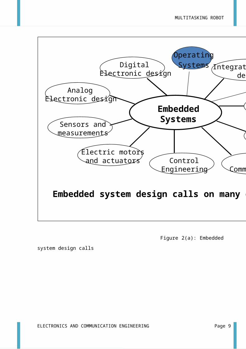
SYSTEM DESIGN CALLS:
Figure 2(a): Embedded system design calls
ELECTRONICS AND COMMUNICATION ENGINEERING Page 5
EmbeddedSystemsComputerArchitectureSoftwareEngineering
Data CommunicationControlEngineeringElectric motorsand actuators
Sensors andmeasurements
AnalogElectronic design
DigitalElectronic design Integrated circuitdesign
Embedded system design calls on many disciplines
Operating Systems
BuildDownload
DebugTools

MULTITASKING ROBOT
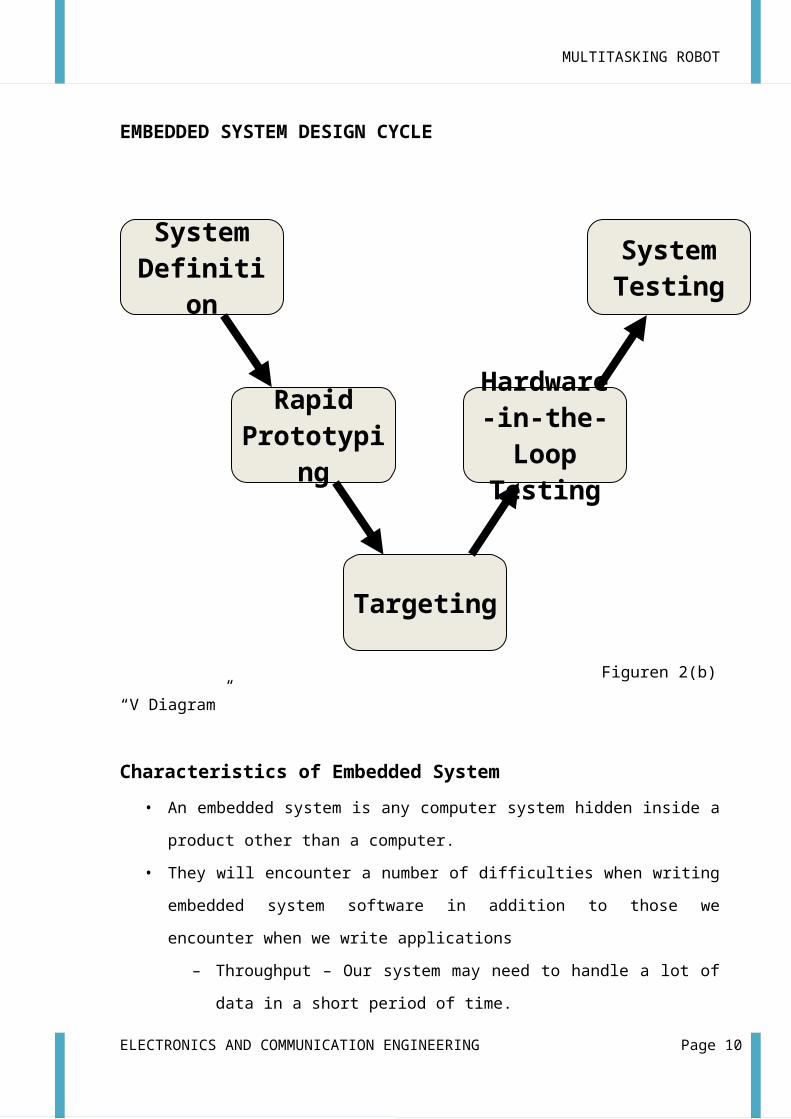
EMBEDDED SYSTEM DESIGN CYCLE
Figuren 2(b) “V Diagram”
Characteristics of Embedded System• An embedded system is any computer system hidden inside a product other than a
computer.
• They will encounter a number of difficulties when writing embedded system software
in addition to those we encounter when we write applications
– Throughput – Our system may need to handle a lot of data in a short period of
time.
– Response–Our system may need to react to events quickly
– Testability–Setting up equipment to test embedded software can be difficult
– Debugability–Without a screen or a keyboard, finding out what the software is
doing wrong (other than not working) is a troublesome problem
– Reliability – embedded systems must be able to handle any situation without
human intervention
– Memory space – Memory is limited on embedded systems, and you must
make the software and the data fit into whatever memory exists
– Program installation – you will need special tools to get your software into
embedded systems
– Power consumption – Portable systems must run on battery power, and the
software in these systems must conserve power
ELECTRONICS AND COMMUNICATION ENGINEERING Page 6
System
Testing
System
Definition
Targeting
Rapid Prototyp
ing
Hardware-in-
the-Loop Testin
g

MULTITASKING ROBOT
– Processor hogs – computing that requires large amounts of CPU time can
complicate the response problem
– Cost – Reducing the cost of the hardware is a concern in many embedded
system projects; software often operates on hardware that is barely adequate
for the job.
• Embedded systems have a microprocessor/ microcontroller and a memory. Some
have a serial port or a network connection. They usually do not have keyboards,
screens or disk drives.
APPLICATIONS
1) Military and aerospace embedded software applications
2) Communicat ion Appl icat ions
3) Indust r ia l automat ion and process control sof tware
4) Mastering the complexity of applications.
5) Reduction of product design time.
6) Real time processing of ever increasing amounts of data.
7) Intelligent, autonomous sensors.
CLASSIFICATION
Real Time Systems.
RTS is one which has to respond to events within a specified deadline.
A right answer after the dead line is a wrong answer.
RTS CLASSIFICATION
Hard Real Time Systems
Soft Real Time System
ELECTRONICS AND COMMUNICATION ENGINEERING Page 7

MULTITASKING ROBOT
HARD REAL TIME SYSTEM
"Hard" real-time systems have very narrow response time.
Example: Nuclear power system, Cardiac pacemaker.
SOFT REAL TIME SYSTEM
"Soft" real-time systems have reduced constrains on "lateness" but still must operate
very quickly and repeatable.
Example: Railway reservation system – takes a few extra seconds the data remains
valid.
ELECTRONICS AND COMMUNICATION ENGINEERING Page 8
MULTITASKING ROBOT
3. PROJECT BLOCK DIAGRAM
ELECTRONICS AND COMMUNICATION ENGINEERING Page 9
MULTITASKING ROBOT
4. HARDWARE REQUIREMENTS
HARDWARE COMPONENTS:
1. VOLTAGE REGULATOR
2. MICROCONTROLLER (89V51RD2)
3. PUSH BUTTONS
4. DTMF DECODER
5. L293D MOTOR DRIVER
6. DC MOTOR
7. INVERTER IC 7404
8. LED
9. 1N4007
10. RESISTORS
11. CAPACITORS
12. BATTERY
ELECTRONICS AND COMMUNICATION ENGINEERING Page 10

MULTITASKING ROBOT
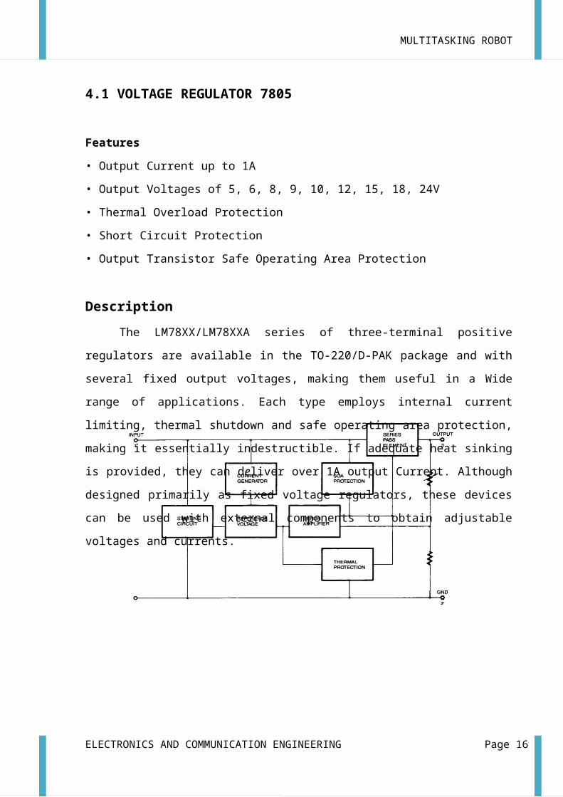
4.1 VOLTAGE REGULATOR 7805
Features
• Output Current up to 1A
• Output Voltages of 5, 6, 8, 9, 10, 12, 15, 18, 24V
• Thermal Overload Protection
• Short Circuit Protection
• Output Transistor Safe Operating Area Protection
DescriptionThe LM78XX/LM78XXA series of three-terminal positive regulators are available in
the TO-220/D-PAK package and with several fixed output voltages, making them useful in a
Wide range of applications. Each type employs internal current limiting, thermal shutdown
and safe operating area protection, making it essentially indestructible. If adequate heat
sinking is provided, they can deliver over 1A output Current. Although designed primarily as
fixed voltage regulators, these devices can be used with external components to obtain
adjustable voltages and currents.
FIG 4.2(a): BLOCK DIAGRAM OF VOLTAGE REGULATOR
ELECTRONICS AND COMMUNICATION ENGINEERING Page 11

MULTITASKING ROBOT
4.2 MICROCONTROLLER 89V51RD2
The 89V51RD2 is a low-power, high-performance CMOS 8-bit microcontroller with
8K bytes of in-system programmable Flash memory. The device is manufactured using
Atmel’s high-density non volatile memory technology and is compatible with the industry
standard 80C51 instruction set and pin out. The on-chip Flash allows the program memory to
be reprogrammed in-system or by a conventional non volatile memory programmer. By
combining a versatile 8-bit CPU with in-system programmable Flash on a monolithic chip,
the Atmel 89V51RD2 is a powerful microcontroller which provides a highly-flexible and
cost-effective solution to many embedded control applications. The 89V51RD2 provides the
following standard features: 8K bytes of Flash, 256 bytes of RAM, 32 I/O lines, Watchdog
timer, two data pointers, three 16-bit timer/counters, a six-vector two-level interrupt
architecture, a full duplex serial port, on-chip oscillator, and clock circuitry. In addition, the
89V51RD2 is designed with static logic for operation down to zero frequency and supports
two software selectable power saving modes. The Idle Mode stops the CPU while allowing
the RAM, timer/counters, serial port, and interrupt system to continue functioning. The
Power-down mode saves the RAM contents but freezes the oscillator, disabling all other chip
functions until the next interrupt or hardware reset.
Features:
• Compatible with MCS®-51 Products
• 8K Bytes of In-System Programmable (ISP) Flash Memory
– Endurance: 10,000 Write/Erase Cycles
• 4.0V to 5.5V Operating Range
• Fully Static Operation: 0 Hz to 33 MHz
• Three-level Program Memory Lock
• 256 x 8-bit Internal RAM
• 32 Programmable I/O Lines
ELECTRONICS AND COMMUNICATION ENGINEERING Page 12
MULTITASKING ROBOT
• Three 16-bit Timer/Counters
• Eight Interrupt Sources
• Full Duplex UART Serial Channel
• Low-power Idle and Power-down Modes
• Interrupt Recovery from Power-down Mode
• Watchdog Timer
• Dual Data Pointer
• Power-off Flag
• Fast Programming Time
• Flexible ISP Programming (Byte and Page Mode)
• Green (Pb/Halide-free) Packaging Option
ELECTRONICS AND COMMUNICATION ENGINEERING Page 13

MULTITASKING ROBOT
Block Diagram of AT89S52:
FIG 4.5(A): BLOCK DIAGRAM OF 89V51RD2
ELECTRONICS AND COMMUNICATION ENGINEERING Page 14

MULTITASKING ROBOT
Pin Configurations of AT89S52
FIG 4.5(b): PIN DIAGRAM OF 89V51RD2
Pin Description:
VCC:
Supply voltage.
GND:
Ground
Port 0:
Port 0 is an 8-bit open drain bidirectional I/O port. As an output port, each pin can
sink eight TTL inputs. When 1s are written to port 0 pins, the pins can be used as high-
impedance inputs. Port 0 can also be configured to be the multiplexed low-order address/data
bus during accesses to external program and data memory. In this mode, P0 has internal pull-
ELECTRONICS AND COMMUNICATION ENGINEERING Page 15
MULTITASKING ROBOT
ups. Port 0 also receives the code bytes during Flash programming and outputs the code bytes
during program verification. External pull-ups are required during program verification.
Port 1:
Port 1 is an 8-bit bidirectional I/O port with internal pull-ups. The Port 1 output
buffers can sink/source four TTL inputs. When 1s are written to Port 1 pins, they are pulled
high by the internal pull-ups and can be used as inputs. As inputs, Port 1 pins that are
externally being pulled low will source current (IIL) because of the internal pull-ups. In
addition, P1.0 and P1.1 can be configured to be the timer/counter 2 external count input
(P1.0/T2) and the timer/counter 2 trigger input (P1.1/T2EX).
Port 2:
Port 2 is an 8-bit bidirectional I/O port with internal pull-ups. The Port 2 output
buffers can sink/source four TTL inputs. When 1s are written to Port 2 pins, they are pulled
high by the internal pull-ups and can be used as inputs. As inputs, Port 2 pins that are
externally being pulled low will source current (IIL) because of the internal pull-ups. Port 2
emits the high-order address byte during fetches from external program memory and during
accesses to external data memory that use 16-bit addresses (MOVX @ DPTR). In this
application, Port 2 uses strong internal pull-ups when emitting 1s. During accesses to external
data memory that use 8-bit addresses (MOVX @ RI), Port 2 emits the contents of the P2
Special Function Register.
Port 3:
Port 3 is an 8-bit bidirectional I/O port with internal pull-ups. The Port 3 output
buffers can sink/source four TTL inputs. When 1s are written to Port 3 pins, they are pulled
high by the internal pull-ups and can be used as inputs. As inputs, Port 3 pins that are
externally being pulled low will source current (IIL) because of the pull-ups.
RST:
Reset input. A high on this pin for two machine cycles while the oscillator is running
resets the device. This pin drives high for 98 oscillator periods after the Watchdog times out.
The DISRTO bit in SFR AUXR (address 8EH) can be used to disable this feature. In the
default state of bit DISRTO, the RESET HIGH out feature is enabled.
ELECTRONICS AND COMMUNICATION ENGINEERING Page 16

MULTITASKING ROBOT
ALE/PROG:
Address Latch Enable (ALE) is an output pulse for latching the low byte of the
address during accesses to external memory. This pin is also the program pulse input (PROG)
during Flash programming.
In normal operation, ALE is emitted at a constant rate of 1/6 the oscillator frequency
and may be used for external timing or clocking purposes. Note, however, that one ALE
pulse is skipped during each access to external data memory.
PSEN:
Program Store Enable (PSEN) is the read strobe to external program memory. When
the AT89S52 is executing code from external program memory, PSEN is activated twice
each machine cycle, except that two PSEN activations are skipped during each access to
external data memory.
EA/VPP:
External Access Enable. EA must be strapped to GND in order to enable the device
to fetch code from external program memory locations starting at 0000H up to FFFFH. Note,
however, that if lock bit 1 is programmed, EA will be internally latched on reset. EA should
be strapped to VCC for internal program executions. This pin also receives the 12-volt
programming enable voltage (VPP) during Flash programming.
XTAL1:
Input to the inverting oscillator amplifier and input to the internal clock operating
circuit.
XTAL2:
Output from the inverting oscillator amplifier
Oscillator Characteristics: XTAL1 and XTAL2 are the input and output, respectively, of an inverting amplifier
which can be configured for use as an on-chip oscillator, as shown in Figure 1. Either a
quartz crystal or ceramic resonator may be used. To drive the device from an external clock
source, XTAL2 should be left unconnected while XTAL1 is driven as shown in Figure 6.2.
ELECTRONICS AND COMMUNICATION ENGINEERING Page 17

MULTITASKING ROBOT
There are no requirements on the duty cycle of the external clock signal, since the input to the
internal clocking circuitry is through a divide-by-two flip-flop, but minimum and maximum
voltage high and low time specifications must be observed.
FIG 4.5(c): Oscillator Connections
FIG 4.5(d): External Clock Drive Configuration
Idle Mode
In idle mode, the CPU puts itself to sleep while all the on chip peripherals remain active.
The mode is invoked by software. The content of the on-chip RAM and all the special
functions registers remain unchanged during this mode. The idle mode can be terminated by
any enabled interrupt or by a hardware reset.
Power down Mode
In the power down mode the oscillator is stopped, and the instruction that invokes
power down is the last instruction executed. The on-chip RAM and Special Function
Registers retain their values until the power down mode is terminated. The only exit from
ELECTRONICS AND COMMUNICATION ENGINEERING Page 18

MULTITASKING ROBOT
power down is a hardware reset. Reset redefines the SFRs but does not change the on-chip
RAM. The reset should not be activated before VCC is restored to its normal operating level
and must be held active long enough to allow the oscillator to restart and stabilize.
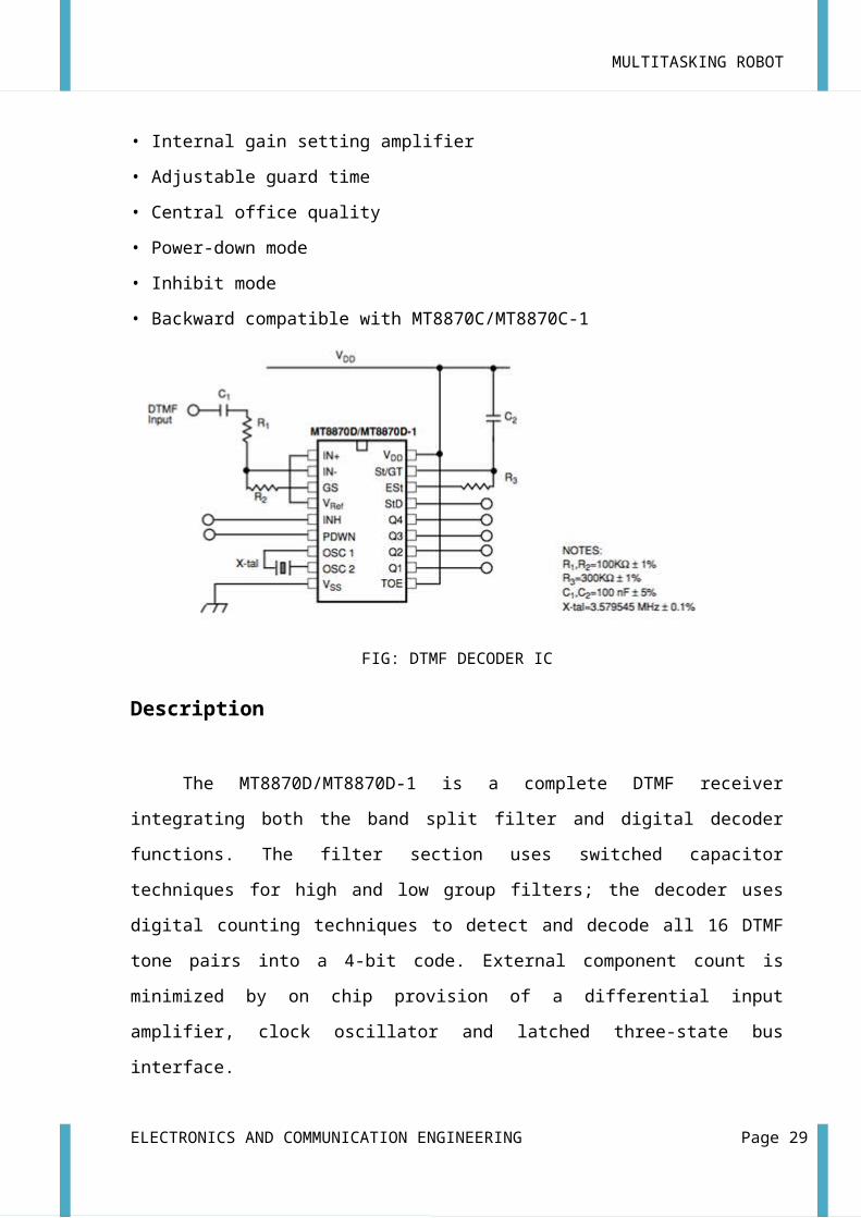
4.4 DTMF DECODER
Introduction
Dual Tone Multiple Frequency (DTMF) decoder IC is used to decode the key strokes
like that of a telephone.
Telephone signalling is based on encoding keypad digits using two sinusoidal of
different frequencies, hence the name DTMF. Each digit is represented by a low frequency
and a high frequency sinusoid. The frequencies used were recommended by AT&T such that
no two frequencies are integral multiples of each other. This facilitates correct decoding even
in the presence of non linearity of filters which cause higher harmonics to be present.
Features
• Complete DTMF Receiver
• Low power consumption
ELECTRONICS AND COMMUNICATION ENGINEERING Page 19

MULTITASKING ROBOT
• Internal gain setting amplifier
• Adjustable guard time
• Central office quality
• Power-down mode
• Inhibit mode
• Backward compatible with MT8870C/MT8870C-1
FIG: DTMF DECODER IC
Description
The MT8870D/MT8870D-1 is a complete DTMF receiver integrating both the band
split filter and digital decoder functions. The filter section uses switched capacitor techniques
for high and low group filters; the decoder uses digital counting techniques to detect and
decode all 16 DTMF tone pairs into a 4-bit code. External component count is minimized by
on chip provision of a differential input amplifier, clock oscillator and latched three-state bus
interface.
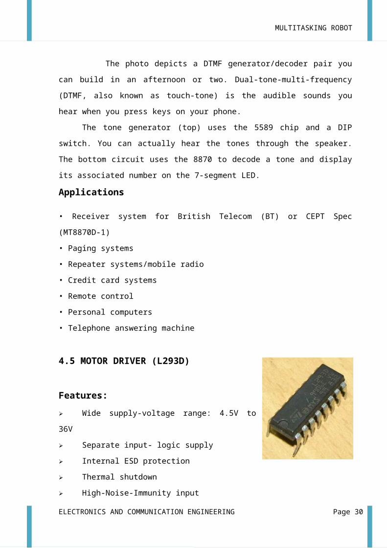
The photo depicts a DTMF generator/decoder pair you can build in an afternoon or
two. Dual-tone-multi-frequency (DTMF, also known as touch-tone) is the audible sounds you
hear when you press keys on your phone.
The tone generator (top) uses the 5589 chip and a DIP switch. You can actually hear
the tones through the speaker. The bottom circuit uses the 8870 to decode a tone and display
its associated number on the 7-segment LED.
Applications
ELECTRONICS AND COMMUNICATION ENGINEERING Page 20

MULTITASKING ROBOT
• Receiver system for British Telecom (BT) or CEPT Spec (MT8870D-1)
• Paging systems
• Repeater systems/mobile radio
• Credit card systems
• Remote control
• Personal computers
• Telephone answering machine
4.5 MOTOR DRIVER (L293D)
Features: Wide supply-voltage range: 4.5V to 36V
Separate input- logic supply
Internal ESD protection
Thermal shutdown
High-Noise-Immunity input
Functional Replacements for SGS L293 and SGS L293D
Output current 1A per channel (600 mA for L293D)
Peak output current 2 A per channel (1.2 A for L293D)
Output clamp diodes for Inductive Transient Suppression(L293D)
DESCRIPTION:
L293D is a dual H-bridge motor driver integrated circuit (IC). Motor drivers act as
current amplifiers since they take a low-current control signal and provide a higher-current
signal. This higher current signal is used to drive the motors.
L293D contains two inbuilt H-bridge driver circuits. In its common mode of operation,
two DC motors can be driven simultaneously, both in forward and reverse direction. The
motor operations of two motors can be controlled by input logic at pins 2 & 7 and 10 & 15.
Input logic 00 or 11 will stop the corresponding motor. Logic 01 and 10 will rotate it in
clockwise and anticlockwise directions, respectively.
ELECTRONICS AND COMMUNICATION ENGINEERING Page 21

MULTITASKING ROBOT
Enable pins 1 and 9 (corresponding to the two motors) must be high for motors to start
operating. When an enable input is high, the associated driver gets enabled. As a result, the
outputs become active and work in phase with their inputs. Similarly, when the enable input
is low, that driver is disabled, and their outputs are off and in the high-impedance state.
Block diagram:
FIG: BLOCK
Pin Diagram:
4.6 DC MOTOR
ELECTRONICS AND COMMUNICATION ENGINEERING Page 22

MULTITASKING ROBOT
A DC motor is an electric motor that runs on direct current (DC) electricity. In any
electric motor, operation is based on simple electromagnetism. A current-carrying conductor
generates a magnetic field; when this is then placed in an external magnetic field, it will
experience a force proportional to the current in the conductor, and to the strength of the
external magnetic field. As you are well aware of from playing with magnets as a kid,
opposite (North and South) polarities attract, while like polarities (North and North, South
and South) repel. The internal configuration of a DC motor is designed to harness the
magnetic interaction between a current-carrying conductor and an external magnetic field to
generate rotational motion.
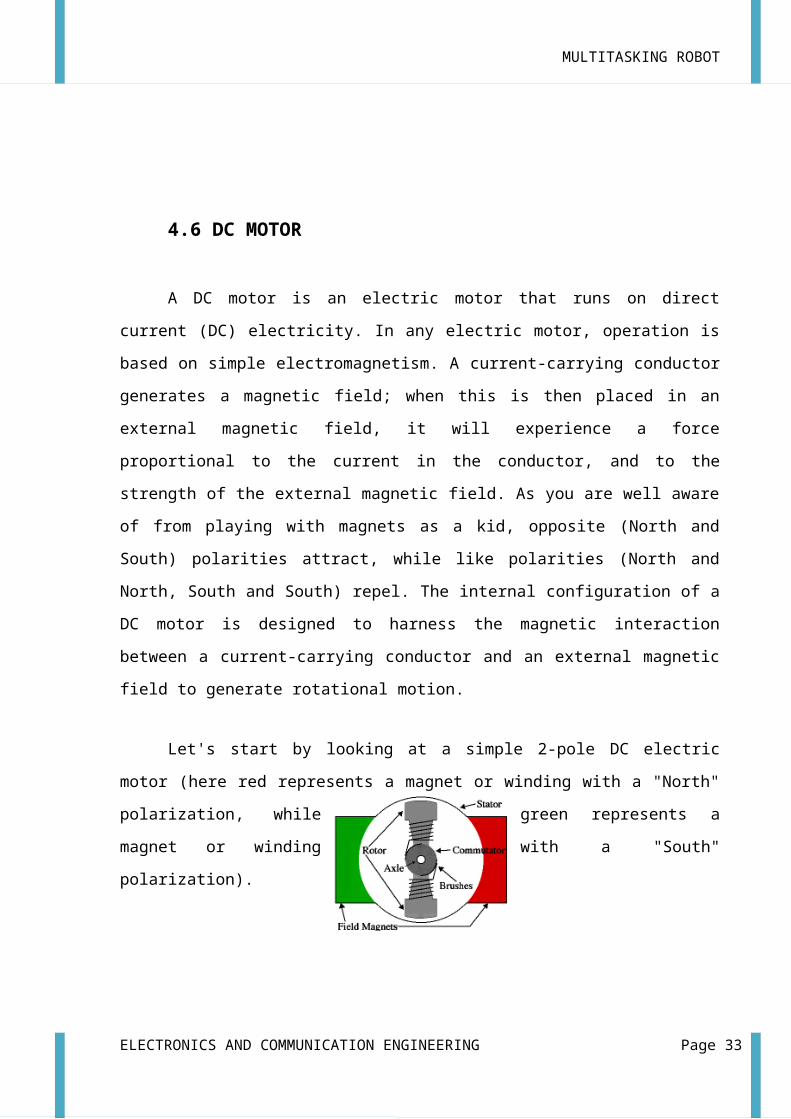
Let's start by looking at a simple 2-pole DC electric motor (here red represents a
magnet or winding with a "North" polarization, while green represents a magnet or winding
with a "South" polarization).
Fig.4.9(c) DC motor
4.7 INVERTER IC 7404
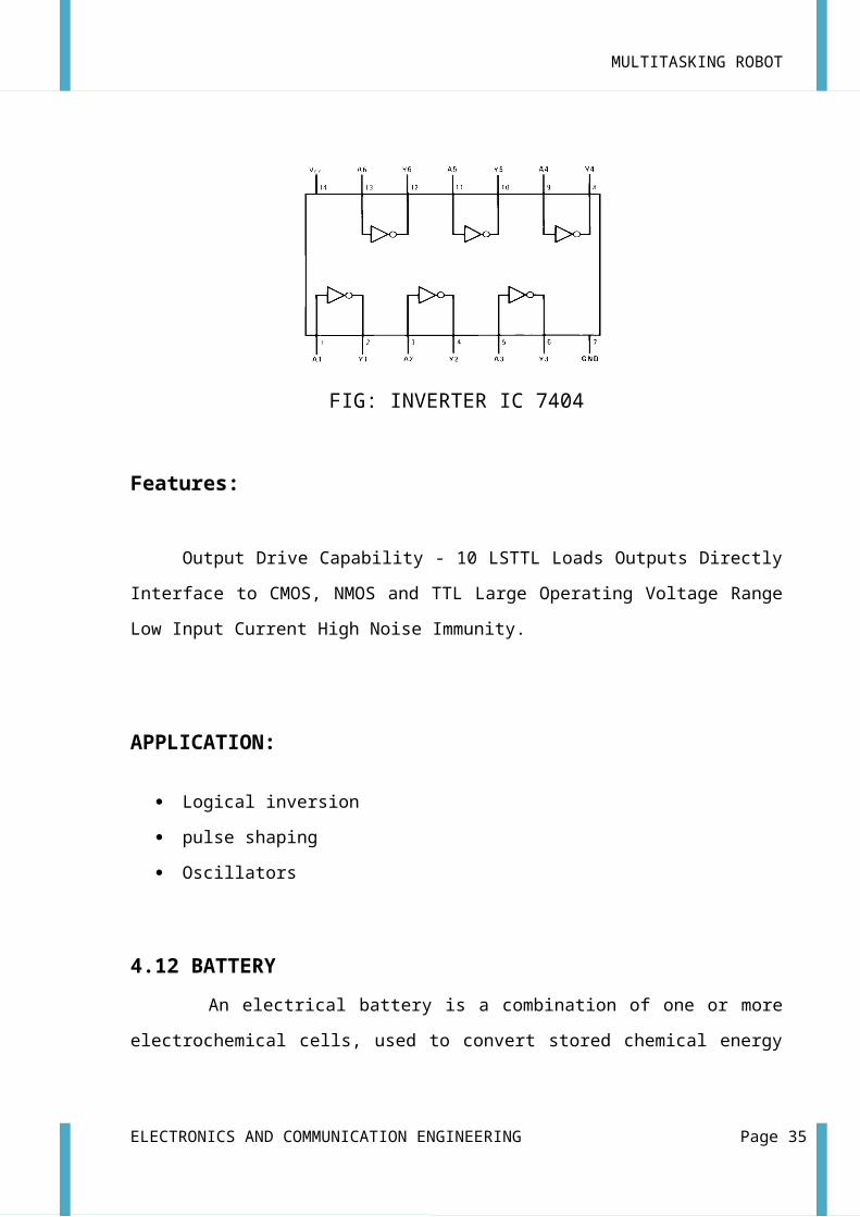
Outputs of one gate can be connected to inputs of another within the same chip or to
another chip as long as they share the same ground. The figure to the left illustrates a basic
circuit showing how to wire inputs and using LEDs to display outputs.
The 7404 is an inverting buffer, especially useful when the output of one circuit
cannot sink much current. A computer's parallel port is a notorious example and can easily
be damaged by excessive current draw. Each of the parallel ports outputs can be connected
to one of the six inputs on the 7404 hex inverter chip. However, more than one 7404 will be
needed to interface all of the parallel port pins.
NOT GATE Logic-Rules:
ELECTRONICS AND COMMUNICATION ENGINEERING Page 23
MULTITASKING ROBOT
The output is the inverse of the input, in other words if the input is HIGH then the out put is
LOW and if the input is LOW the output is HIGH.
FIG: INVERTER IC 7404
Features:
Output Drive Capability - 10 LSTTL Loads Outputs Directly Interface to CMOS,
NMOS and TTL Large Operating Voltage Range Low Input Current High Noise Immunity.
APPLICATION:
Logical inversion
pulse shaping
Oscillators
4.12 BATTERYAn electrical battery is a combination of one or more electrochemical cells, used
to convert stored chemical energy into electrical energy. The battery has become a common
power source for many household and industrial applications.
ELECTRONICS AND COMMUNICATION ENGINEERING Page 24
MULTITASKING ROBOT
Working of battery:
A battery is a device that converts chemical energy directly to electrical energy. It
consists of a number of voltaic cells; each voltaic cell consists of two half cells connected in
series by a conductive electrolyte containing anions and cat ions. One half-cell includes
electrolyte and the electrode to which anions (negatively-charged ions) migrate, i.e. the anode
or negative electrode; the other half-cell includes electrolyte and the electrode to which cat
ions (positively-charged ions) migrate, i.e. the cathode or positive electrode. Each half cell
has an electromotive force (or emf), determined by its ability to drive electric current from
the interior to the exterior of the cell. The net emf of the cell is the difference between the
emfs of its half-cells. Therefore, if the electrodes have emfs and, in other words, the net emf
is the difference between the reduction potentials of the half-reactions.
Principle of operation
A battery is a device that converts chemical energy directly to electrical energy. It
consists of a number of voltaic cells; each voltaic cell consists of two half cells connected in
series by a conductive electrolyte containing anions and cations. One half-cell includes
electrolyte and the electrode to which anions (negatively charged ions) migrate, i.e., the
anode or negative electrode; the other half-cell includes electrolyte and the electrode to which
cations (positively charged ions) migrate, i.e., the cathode or positive electrode. In the redox
reaction that powers the battery, cations are reduced (electrons are added) at the cathode,
while anions are oxidized (electrons are removed) at the anode. The electrodes do not touch
each other but are electrically connected by cells allows ions to flow, but prevents mixing of
the electrolytes.
ELECTRONICS AND COMMUNICATION ENGINEERING Page 25

MULTITASKING ROBOT
5.SOFTWARE REQUIREMENTS
5.1 INTRODUCTION TO KEIL MICRO VISION (IDE)
Keil an ARM Company makes C compilers, macro assemblers, real-time kernels,
debuggers, simulators, integrated environments, evaluation boards, and emulators for
ARM7/ARM9/Cortex-M3, XC16x/C16x/ST10, 251, and 8051 MCU families.
Keil development tools for the 8051 Microcontroller Architecture support every level
of software developer from the professional applications engineer to the student just learning
about embedded software development. When starting a new project, simply select the
microcontroller you use from the Device Database and the µVision IDE sets all compiler,
assembler, linker, and memory options for you.
Keil is a cross compiler. So first we have to understand the concept of compilers and
cross compilers. After then we shall learn how to work with keil.
5.2 Concept Of Compiler Compilers are programs used to convert a High Level Language to object code.
Desktop compilers produce an output object code for the underlying microprocessor, but not
for other microprocessors. I.E the programs written in one of the HLL like ‘C’ will compile
the code to run on the system for a particular processor like x86 (underlying microprocessor
in the computer). For example compilers for Dos platform is different from the Compilers for
Unix platform So if one wants to define a compiler then compiler is a program that translates
source code into object code.
5.5 Building an Application in µVision2
To build (compile, assemble, and link) an application in µVision2, you must:
1. Select Project -(forexample,166\EXAMPLES\HELLO\HELLO.UV2).
2. Select Project - Rebuild all target files or Build target.µVision2 compiles, assembles,
and links the files in your project.
ELECTRONICS AND COMMUNICATION ENGINEERING Page 26
MULTITASKING ROBOT
5.6 Creating Your Own Application in µVision2 To create a new project in µVision2, you must:
1. Select Project - New Project.
2. Select a directory and enter the name of the project file.
3. Select Project - Select Device and select an 8051, 251, or C16x/ST10 device from the
Device Database™.
4. Create source files to add to the project.
5. Select Project - Targets, Groups, Files. Add/Files, select Source Group1, and add the
source files to the project.
6. Select Project - Options and set the tool options. Note when you select the target
device from the Device Database™ all special options are set automatically. You
typically only need to configure the memory map of your target hardware. Default
memory model settings are optimal for most applications.
7. Select Project - Rebuild all target files or Build target.
5.7 Debugging an Application in µVision2To debug an application created using µVision2, you must:
1. Select Debug - Start/Stop Debug Session.
2. Use the Step toolbar buttons to single-step through your program. You may enter G,
main in the Output Window to execute to the main C function.
3. Open the Serial Window using the Serial #1 button on the toolbar.
Debug your program using standard options like Step, Go, Break, and so on.
5.8 Starting µVision2 and Creating a ProjectµVision2 is a standard Windows application and started by clicking on the program
icon. To create a new project file select from the µVision2 menu Project – New Project….
This opens a standard Windows dialog that asks you for the new project file name. We
suggest that you use a separate folder for each project. You can simply use the icon Create
New Folder in this dialog to get a new empty folder. Then select this folder and enter the file
name for the new project, i.e. Project1. µVision2 creates a new project file with the name
PROJECT1.UV2 which contains a default target and file group name. You can see these
names in the Project.
ELECTRONICS AND COMMUNICATION ENGINEERING Page 27

MULTITASKING ROBOT
5.9 Window – Files.Now use from the menu Project – Select Device for Target and select a CPU for your
project. The Select Device dialog box shows the µVision2 device data base. Just select the
microcontroller you use. We are using for our examples the Philips 80C51RD+ CPU. This
selection sets necessary tool Options for the 80C51RD+ device and simplifies in this way the
tool Configuration.
5.10 Building Projects and Creating a HEX FilesTypical, the tool settings under Options – Target are all you need to start a new
application. You may translate all source files and line the application with a click on the
Build Target toolbar icon. When you build an application with syntax errors, µVision2 will
display errors and warning messages in the Output Window – Build page. A double click on
a message line opens the source file on the correct location in a µVision2 editor window.
Once you have successfully generated your application you can start debugging.
5.11 Database selectionYou have made when you create your project target. Refer to page 58 for more Information
about selecting a device. You may select and display the on-chip peripheral components
using the Debug menu. You can also change the aspects of each peripheral using the controls
in the dialog boxes.
5.13 Start DebuggingYou start the debug mode of µVision2 with the Debug – Start/Stop Debug Session
Command. Depending on the Options for Target – Debug Configuration, µVision2 will load
the application program and run the startup code µVision2 saves the editor screen layout and
restores the screen layout of the last debug session. If the program execution stops, µVision2
opens an editor window with the source text or shows CPU instructions in the disassembly
window. The next executable statement is marked with a yellow arrow. During debugging,
most editor features are still available.
ELECTRONICS AND COMMUNICATION ENGINEERING Page 28
MULTITASKING ROBOT
5.14 Disassembly WindowThe Disassembly window shows your target program as mixed source and assembly
program or just assembly code. A trace history of previously executed instructions may be
displayed with Debug – View Trace Records. To enable the trace history, set Debug –
Enable/Disable Trace Recording.
5.15 Embedded C Use of embedded processors in passenger cars, mobile phones, medical equipment,
aerospace systems and defense systems is widespread, and even everyday domestic
appliances such as dish washers, televisions, washing machines and video recorders now
include at least one such device.
Because most embedded projects have severe cost constraints, they tend to use low-
cost processors like the 8051 family of devices considered in this book. These popular chips
have very limited resources available most such devices have around 256 bytes (not
megabytes!) of RAM, and the available processor power is around 1000 times less than that
of a desktop processor. As a result, developing embedded software presents significant new
challenges, even for experienced desktop programmers. If you have some programming
experience - in C, C++ or Java - then this book and its accompanying CD will help make
your move to the embedded world as quick and painless as possible.
ELECTRONICS AND COMMUNICATION ENGINEERING Page 29
MULTITASKING ROBOT
6.SCHEMATIC DIAGRAM
6.1 DESCRIPTION POWER SUPPLY
This project uses a 6V battery for power supply. A silicon diode is used in series for
getting approximately 5V . One LED is connected of this 5V point in series with a resistor of
330Ω to the ground i.e., negative voltage to indicate 5V power supply availability.
STANDARD CONNECTIONS TO 8051 SERIES MICRO
CONTROLLER
ATMEL series of 8051 family of micro controllers need certain standard
connections. The actual number of the Microcontroller could be “89C51” , “89C52”,
“89S51”, “89S52”, and as regards to 20 pin configuration a number of “89C2051”. The 4 set
of I/O ports are used based on the project requirement. Every microcontroller requires a
ELECTRONICS AND COMMUNICATION ENGINEERING Page 30

MULTITASKING ROBOT
timing reference for its internal program execution therefore an oscillator needs to be
functional with a desired frequency to obtain the timing reference as t =1/f.
A crystal ranging from 2 to 20 MHz is required to be used at its pin number 18 and 19
for the internal oscillator. It may be noted here the crystal is not to be understood as crystal
oscillator It is just a crystal, while connected to the appropriate pin of the microcontroller it
results in oscillator function inside the microcontroller.
RESET
Pin no 9 is provided with an resset arrangement by a combination of an electrolytic
capacitor and a register forming RC time constant. At the time of switch on, the capacitor
gets charged, and it behaves as a full short circuit from the positive to the pin number 9. After
the capacitor gets fully charged the current stops flowing and pin number 9 goes low which is
pulled down by a 10k resistor to the ground. This arrangement of reset at pin 9 going high
initially and then to logic 0 i.e., low helps the program execution to start from the beginning.
In absence of this the program execution could have taken place arbitrarily anywhere from
the program cycle.
For example: A 10µF capacitor and a 10kΩ resistor would render a 100ms time to pin
number 9 from logic high to low, there after the pin number 9 remains low.
External Access(EA):
Pin no 31 of 40 pin 8051 microcontroller termed as EA¯ is required to be connected to 5V for
accessing the program form the on-chip program memory. If it is connected to ground then
the controller accesses the program from external memory. However as we are using the
internal memory it is always connected to +5V.
L293D MOTOR DRIVER
L293D has 2 set of arrangements where one set has input 1, input 2, output 1
and output 2 and other set has input 3, input 4, output 3 and output 4, according to
block diagram if pin no 2 & 7 are high then pin no 3 & 6 are also high.
If enable 1 and pin number 2 are high leaving pin number 7 as low then the
motor rotates in forward direction.
ELECTRONICS AND COMMUNICATION ENGINEERING Page 31

MULTITASKING ROBOT
If enable 2 and pin number 10 are high leaving pin number 15 as low then the
motor rotates in forward direction.
If enable 1 and pin number 2 are low leaving pin number 7 as high then the
motor rotates in reverse direction.
If enable 2 and pin number 15 are high leaving pin number 10 as low then the
motor rotates in forward direction.
OPERATION EXPLANATION
Connections:
The output of the power supply which is 5v is connected to the 40 pin of
Microcontroller and GND I connected to its 20th pin. Port 1.0 of Microcontroller is connected
to transistor Q1 that drives the laser. Port 2.2, 2.3, 2.4 of Microcontroller are connected to pin
number 9, 15, 10 of L293D i.e., Motor driver IC. Port 2.5, 2.6, 2.7 of Microcontroller are
connected to pin number 7, 2, 1 of Motor driver IC L293D. Port 3.1, 3.2 of Microcontroller is
connected to pin number 13, 12, 11 of DTMF MT8870. Port 3.3 of Microcontroller is
connected to pin 10 of DTMF.
ELECTRONICS AND COMMUNICATION ENGINEERING Page 32
MULTITASKING ROBOT
Working:
DTMF DECODER
After the call is answered by the mobile phone the tone command sent by the sender is
received at the ear phone socket which is fed to pin no 2 of DTMF decoder
MT8870/HT9170through series resistor and capacitor. The project uses DTMF technology for
decoding tone commands by a DTMF decoder IC MT8870. This develops a 4 bit binary data
corresponding to the number related to the tone received at its pin 2 through a high pass filter
of 0.47 Mf and 1K resistor in series.
Operation:One mobile phone is used on the robotic vehicle with its audio output from the earphone
socket connected to pin2 of DTMF IC in series with a high pass filter as noted above. The tip
and GND thus formed the input tone command to the DTMF decoder IC. So while a call is
established from a calling cell phone to an installed cell phone which is kept on auto answer
mode gets activated, as if the call is answered. Now any number by the sending cell phone is
pressed the corresponding tone is available at the receivers cell phone (which is connected to
the robot) thus forms an input tone to the DTMF decoder the output from which is fed to the
controller through inverter IC 7404. The program while executed makes the motor run
forward, backward, left, right as per the command from the senders end. The commands are 2
ELECTRONICS AND COMMUNICATION ENGINEERING Page 33
MULTITASKING ROBOT
for forward, 5 for backward, 1 for left and 3 for right and star (*) for stop. Thus the robot
operates as per the command given in the program.
ELECTRONICS AND COMMUNICATION ENGINEERING Page 34
MULTITASKING ROBOT
7. LAYOUT
FIG 7: LAYOUT DIAGRAM
ELECTRONICS AND COMMUNICATION ENGINEERING Page 35

MULTITASKING ROBOT
8.CODING
ELECTRONICS AND COMMUNICATION ENGINEERING Page 36
MULTITASKING ROBOT
ELECTRONICS AND COMMUNICATION ENGINEERING Page 37

MULTITASKING ROBOT
ELECTRONICS AND COMMUNICATION ENGINEERING Page 38
MULTITASKING ROBOT
10.HARDWARE TESTING
10.1 CONTINUITY TEST:
In electronics, a continuity test is the checking of an electric circuit to see if current
flows (that it is in fact a complete circuit). A continuity test is performed by placing a small
voltage (wired in series with an LED or noise-producing component such as a piezoelectric
speaker) across the chosen path. If electron flow is inhibited by broken conductors, damaged
components, or excessive resistance, the circuit is "open".
This test is the performed just after the hardware soldering and configuration has been
completed. This test aims at finding any electrical open paths in the circuit after the soldering.
Many a times, the electrical continuity in the circuit is lost due to improper soldering, wrong
and rough handling of the PCB, improper usage of the soldering iron, component failures and
presence of bugs in the circuit diagram.
10.2 POWER ON TEST:
This test is performed to check whether the voltage at different terminals is according
to the requirement or not. We take a multi meter and put it in voltage mode. First of all check
the voltage across the battery terminal whether it is fully charged or not, the battery used in
this project is 12V, so touch the ‘red terminal’ of battery with ‘red probe’ of multi meter and
touch ‘black terminal’ of battery with ‘black probe’ of multi meter, if 12V is being displayed
on multi meter screen then we can proceed for next steps.
Now we have to check whether the LEDs are in working condition or not, Red LED
or IR LED or Photo diode has got one ‘longer leg’ and one ‘shorter leg’. Longer leg is
positive terminal of LED and shorter leg is negative terminal.
Now solder Red LED into PCB, remember ‘longer leg’ of LED should be inserted into
positive marking on PCB and ‘shorter leg’ should be inserted into other hole of LED marking
on PCB. Now after soldering LED with a series resistor apply battery voltage to the board
and see whether the LED is glowing or not.
ELECTRONICS AND COMMUNICATION ENGINEERING Page 39

MULTITASKING ROBOT
APPLICATIONS Military surveillance.
Space Exploration.
Hazardous Area Maintenance like Nuclear Power Reactors.
Mining.
Hospitals- To Maintain Sterile Environment.
Industrial Automated Equipment Carriers.
ELECTRONICS AND COMMUNICATION ENGINEERING Page 40
MULTITASKING ROBOT
ADVANTAGES..
Circuit is very simple.
Component used are economical.
Compact, Power Efficient.
No Manual Interpretation Reqttuired.
Accuracy Is Very High.
Can Be Used In All Kinds Of Environment.
Robots never get sick or need to rest, so they can work 24 hours a day, 7 days a week.
ELECTRONICS AND COMMUNICATION ENGINEERING Page 41

MULTITASKING ROBOT
Conclusion
A multitask robot was designed in the project. Using the RF remote control and
sensors to sense the path and obstacles, controller program was designed so as to enable the
microcontroller to control robot, using RF remote and movement of the robot and move when
there is no obstacle in the path.
ELECTRONICS AND COMMUNICATION ENGINEERING Page 42

MULTITASKING ROBOT
RESULT
The project has been accomplished with the help of KEIL C compiler and ATMEL
programmer. The project has been tested successfully and has been approved by the
concerned project guides.
13.BIBLIOGRAPHY
TEXT BOOKS REFERED:
1. “The 8051 Microcontroller and Embedded systems” by Muhammad Ali Mazidi and Janice
Gillispie Mazidi , Pearson Education.
2. ATMEL 89S52 Data Sheets.
WEBSITES
www.atmel.com
www.beyondlogic.org
www.wikipedia.org
www.howstuffworks.com
www.alldatasheets.com
ELECTRONICS AND COMMUNICATION ENGINEERING Page 43