Final ppt
49
MASTER THESIS PRESENTATION
-
Upload
sarangua-enkhbaatar -
Category
Business
-
view
1.363 -
download
0
Transcript of Final ppt
MASTER THESIS PRESENTATION
ASIA UNIVERSITY
COMPUTER SCIENCE ENGINEERING DEPARTMENT
THESIS COMMITTEE1. PROFESSOR DR. GENE SHEU2. PROFESSOR SHAO MING YANG3. PROFESSOR HSIN-CHIANG YOU
ADVISOR: PROFESSOR DR GENE SHEU BY: SARANGUA ENKHBAATAR
A NOVEL ESD DESIGN FOR 800V LDMOS WITH ROBUSTNESS
2

OUTLINE
Introduction
Abstract
Device Structure
Research approach and methodology
Simulation results
Conclusions
3 A NOVEL ESD DESIGN FOR 800V LDMOS WITH ROBUSTNESS

OBJECTIVE
In this thesis a 800V LDMOS with ESD robustness technique is studied.
LDMOS Device with an adding thin p+ insertion butting N+ drain region
Comparison with ESD Test result with conventional structure
Using thermodynamic /continue mode to simulate the device performance after HBM stress with 4K,6K and 8K
The hot spots from each ESD stress can indicate the ESD robustness
05/27/10A NOVEL ESD DESIGN FOR 800V LDMOS WITH ROBUSTNESS
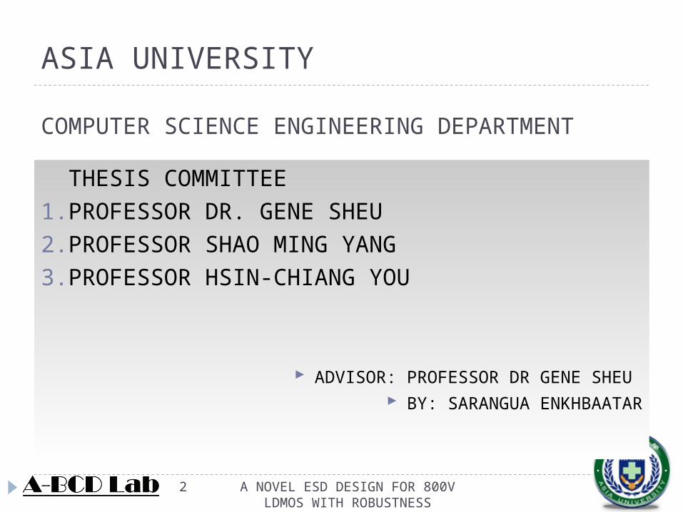
High Voltage LDMOS with optimized ESD robustness is proposed. By comparison with implanting a butting thin P+ at the drain region and compare the ESD performance with the conventional drain implant devices
By HBM test . The novel device deliver better ESD robustness,
with an optimized structure for 800V LDMOS: LDMOS with different structures have different
discharge limits under ESD stress. Some devices are burned out when second breakdown occurs.
5 A NOVEL ESD DESIGN FOR 800V LDMOS WITH ROBUSTNESS
Basic ConceptThe ESD problem for UHV 800V device has
been reliability problem due to the high N-drift resistance and high trigger voltage
The improvement can be a PBL structure, N+ buried layer ..etc
This study is to implement a butting thin P+ layer to Drain for improving current flow with ESD stress.
6 A NOVEL ESD DESIGN FOR 800V LDMOS WITH ROBUSTNESS

LDMOS (Lateral Diffused Metal Oxide Semiconductor) transistor is mainly used in the Ultra high voltage application.
The two major important features specifications of a LDMOS are
low on-resistance (Ron) and high breakdown voltage.
7 A NOVEL ESD DESIGN FOR 800V LDMOS WITH ROBUSTNESS

ESD - Electro-Static Discharge.
What is ESD ?
ESD - Electro-Static Discharge.
ESD is a transient discharge of static charge that arises
from either human handling or a machine contact.
Although ESD is the result of a static potential in a
charged object, the energy dissipated and damages
made are mainly due to the current flowing through ICs
during discharge.
8 A NOVEL ESD DESIGN FOR 800V LDMOS WITH ROBUSTNESS
STATEMENT OF THE PROBLEM
The major problem for 800V UHV LDMOS is the
ESD robustness since the Ndrift is high
resistive ,and the current flowline is not directly
toward to the source contact for power
dissipation.
05/27/10A NOVEL ESD DESIGN FOR 800V LDMOS WITH ROBUSTNESS

ESD Drain (N+) Implant (The conventional)Drain
SourceGate
10 A NOVEL ESD DESIGN FOR 800V LDMOS WITH ROBUSTNESS

800V ESD robustness comparison ESD Drain Implant current potential P+ Insertion at Drain current potential
11 A NOVEL ESD DESIGN FOR 800V LDMOS WITH ROBUSTNESS

Device structureWe use an innovative 800V ldmos device
structure developed by our Lab for achieving best performance for both Breakdown Voltage and Rdson
We will then adding a butting P+ structure to N+ drain and investigate the current flowline after the stress.
12 A NOVEL ESD DESIGN FOR 800V LDMOS WITH ROBUSTNESS
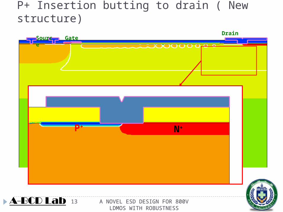
P+ Insertion butting to drain ( New structure)
Drain
P+ N+
Source Gate
13 A NOVEL ESD DESIGN FOR 800V LDMOS WITH ROBUSTNESS
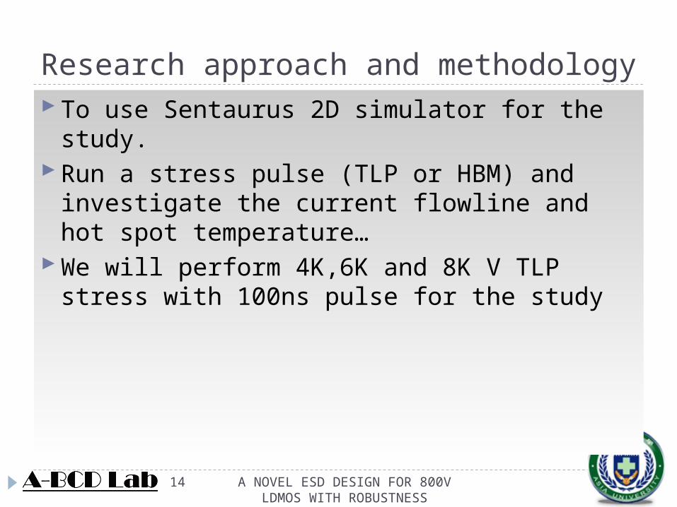
Research approach and methodologyTo use Sentaurus 2D simulator for the study.Run a stress pulse (TLP or HBM) and
investigate the current flowline and hot spot temperature…
We will perform 4K,6K and 8K V TLP stress with 100ns pulse for the study
14 A NOVEL ESD DESIGN FOR 800V LDMOS WITH ROBUSTNESS
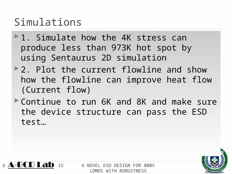
Simulations1. Simulate how the 4K stress can produce
less than 973K hot spot by using Sentaurus 2D simulation
2. Plot the current flowline and show how the flowline can improve heat flow (Current flow)
Continue to run 6K and 8K and make sure the device structure can pass the ESD test…
15 A NOVEL ESD DESIGN FOR 800V LDMOS WITH ROBUSTNESS
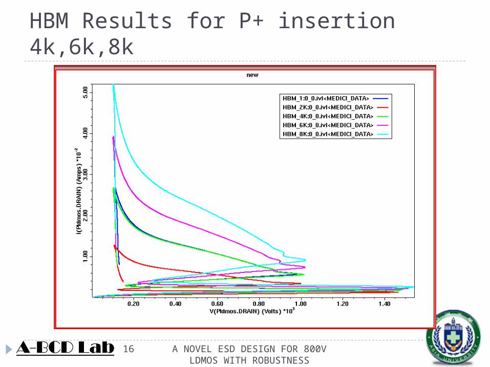
HBM Results for P+ insertion 4k,6k,8k
16 A NOVEL ESD DESIGN FOR 800V LDMOS WITH ROBUSTNESS
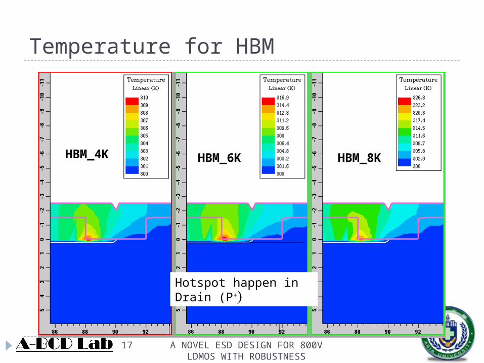
Temperature for HBM
Hotspot happen in Drain (P+)
HBM_4K HBM_6K HBM_8K
17 A NOVEL ESD DESIGN FOR 800V LDMOS WITH ROBUSTNESS
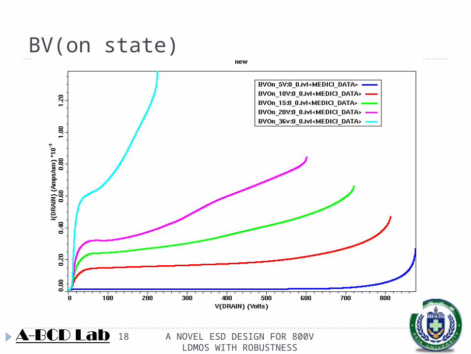
BV(on state)
18 A NOVEL ESD DESIGN FOR 800V LDMOS WITH ROBUSTNESS

Total current flow (P+ Insertion)
The parasitic vertical PNP turns on
19 A NOVEL ESD DESIGN FOR 800V LDMOS WITH ROBUSTNESS

Total Current at ESD with conventional structure
Breakdown SnapbackAfter Breakdown before Snapbak
20 A NOVEL ESD DESIGN FOR 800V LDMOS WITH ROBUSTNESS

Breakdown (P+ Insertion/conventional structure )
21 A NOVEL ESD DESIGN FOR 800V LDMOS WITH ROBUSTNESS
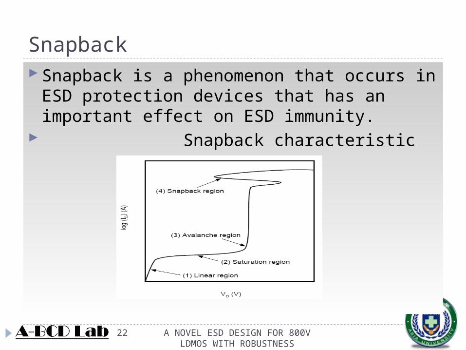
SnapbackSnapback is a phenomenon that occurs in ESD
protection devices that has an important effect on ESD immunity.
Snapback characteristic
22 A NOVEL ESD DESIGN FOR 800V LDMOS WITH ROBUSTNESS

After breakdown and before Snapback (P+ Insertion/ESD implant)
23 A NOVEL ESD DESIGN FOR 800V LDMOS WITH ROBUSTNESS
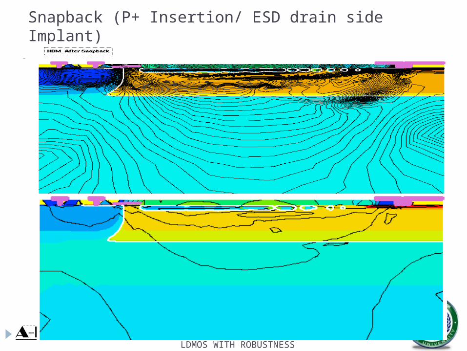
Snapback (P+ Insertion/ ESD drain side Implant)
24 A NOVEL ESD DESIGN FOR 800V LDMOS WITH ROBUSTNESS

HBM-before snapback_4k/ after snapback_4k current potential
25 A NOVEL ESD DESIGN FOR 800V LDMOS WITH ROBUSTNESS

Total Current
26 A NOVEL ESD DESIGN FOR 800V LDMOS WITH ROBUSTNESS

Electron Potential
27 A NOVEL ESD DESIGN FOR 800V LDMOS WITH ROBUSTNESS

BV on conventional structure
05/27/10A NOVEL ESD DESIGN FOR 800V LDMOS WITH ROBUSTNESS

BV on continuation mode
29 A NOVEL ESD DESIGN FOR 800V LDMOS WITH ROBUSTNESS
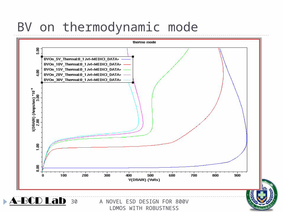
BV on thermodynamic mode
30 A NOVEL ESD DESIGN FOR 800V LDMOS WITH ROBUSTNESS

Label on state 5v, 10v electron potential
31 A NOVEL ESD DESIGN FOR 800V LDMOS WITH ROBUSTNESS

Breakdown(off) Current Potential
32 A NOVEL ESD DESIGN FOR 800V LDMOS WITH ROBUSTNESS

Breakdown Voltage (BVOff)
33 A NOVEL ESD DESIGN FOR 800V LDMOS WITH ROBUSTNESS

Electric Field
Cutline on the surface
Cutline is on the surface of the device we can see the electric field distribution
34 A NOVEL ESD DESIGN FOR 800V LDMOS WITH ROBUSTNESS

Breakdown Voltage (BVOff)Total Current
35 A NOVEL ESD DESIGN FOR 800V LDMOS WITH ROBUSTNESS

Breakdown Voltage (BVOff)Current Potential
36 A NOVEL ESD DESIGN FOR 800V LDMOS WITH ROBUSTNESS

Ron
25 1741076371.4
811.0cmm
eRon
37 A NOVEL ESD DESIGN FOR 800V LDMOS WITH ROBUSTNESS
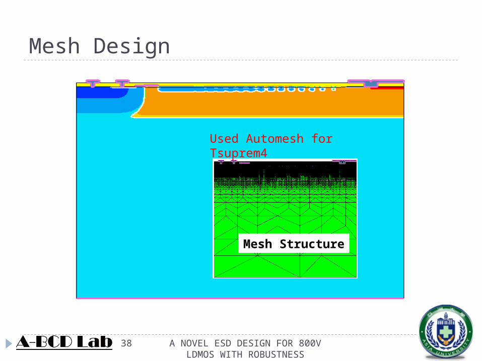
Mesh Design
Used Automesh for Tsuprem4
Mesh Structure
38 A NOVEL ESD DESIGN FOR 800V LDMOS WITH ROBUSTNESS
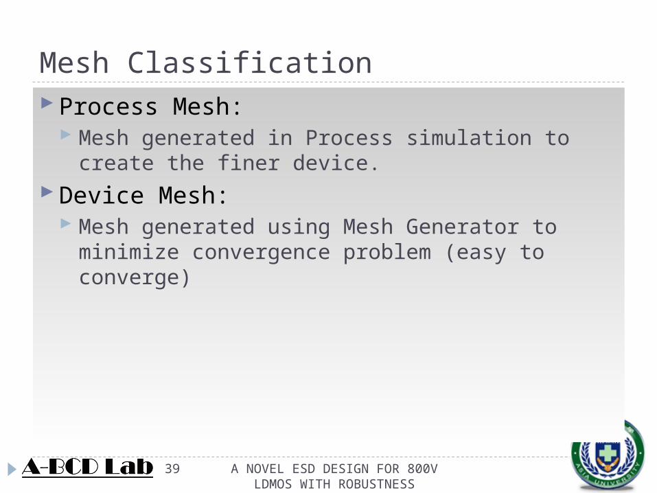
Mesh ClassificationProcess Mesh:
Mesh generated in Process simulation to create the finer device.
Device Mesh: Mesh generated using Mesh Generator to
minimize convergence problem (easy to converge)
39 A NOVEL ESD DESIGN FOR 800V LDMOS WITH ROBUSTNESS
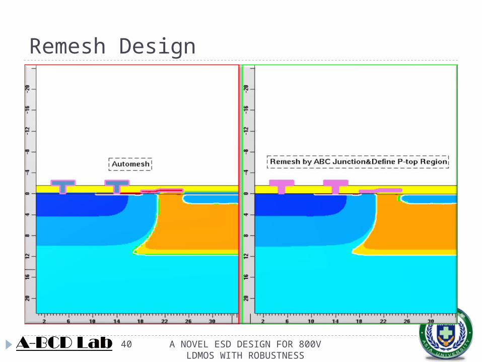
Remesh Design
40 A NOVEL ESD DESIGN FOR 800V LDMOS WITH ROBUSTNESS
Mesh Strategy Objectives In the Process Simulation
smooth Junction finer Doping profile gradient Perfect Boundary (Material Bending)
In the Device Simulation Optimize edges and nodes Low CPU time and Memory consumption easy to converge
41 A NOVEL ESD DESIGN FOR 800V LDMOS WITH ROBUSTNESS

The results and conclusions The innovative structure is no cost addition
since we use P+ mask for the butting P+No additional processThe device can pass HBM test (4K,6K and 8K) It is a manufactuable device and suggest to
have silicon test for further verifications…
42 A NOVEL ESD DESIGN FOR 800V LDMOS WITH ROBUSTNESS

05/27/10A NOVEL ESD DESIGN FOR 800V LDMOS WITH ROBUSTNESS

Electrostatic Discharge Protection
A NOVEL ESD DESIGN FOR 800V LDMOS WITH ROBUSTNESS
44

Electrostatic Discharge Protection
OUTLINE
Introduction to ESD
Principle Sources of ESD in ICs
ESD Models
ESD Protection Mechanisms
45 A NOVEL ESD DESIGN FOR 800V LDMOS WITH ROBUSTNESS
ESD - Electro-Static Discharge. Most ESD damages are thermally initiated in the
form of device / interconnect burn-out or oxide break-down. The basic phenomenon of ESD is that is a large amount of heat is generated in a localized volume significantly faster than it can be removed, leading to a temperature in excess of the materials’ safe operating limits.
ESD Damagespn-junction may melt.Gate oxide may have void formation.Metal interconnects & Vias may melt or
vaporization, leading to shorts or opens.Gate-oxide breakdown is another form of ESD
damage. 46 A NOVEL ESD DESIGN FOR 800V LDMOS WITH ROBUSTNESS

Principle Sources of ESD in ICs• Human Handling
A person walking on a synthetic floor can accumulated up to 20 kV. This voltage is discharged when the person touches an object that is sufficiently at ground. Charge exchange occurs between the person and the object in a very short time duration (10 ns - 100 ns). The charging current is approximately 1A - 10A, depending upon the time constant.
• Test and Handling Systems
Equipment can accumulate static charge due to improper grounding. The charge is transmitted through ICs when it is picked up for placement in test sockets.
• IC Itself is Charged During Transport / Contact With Charged Objects
ICs remain charged until they come into contact with a grounded surface (large metal plates /test sockets). Charge is discharged through the pins of ICs. Large currents in the internal interconnects can result in high voltage inside the devices which can cause damage to thin dielectrics and insulators.47 A NOVEL ESD DESIGN FOR 800V
LDMOS WITH ROBUSTNESS
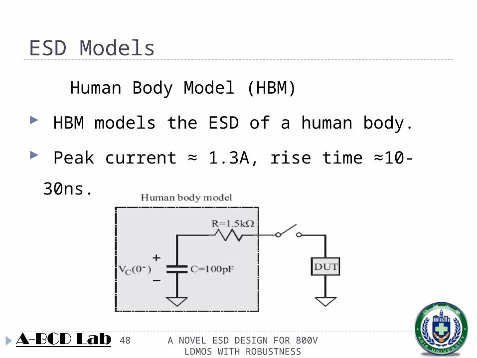
ESD Models
Human Body Model (HBM)
HBM models the ESD of a human body.
Peak current ≈ 1.3A, rise time ≈10-30ns.
48 A NOVEL ESD DESIGN FOR 800V LDMOS WITH ROBUSTNESS
ESD Protection Mechanisms (cont’d)
Current Limiting Characteristics of n-well
Resistors
Impact Ionization
Avalanche Multiplication of pn-junctions
First Breakdown (Avalanche Breakdown)
Second Breakdown (Thermal Breakdown)
49 A NOVEL ESD DESIGN FOR 800V LDMOS WITH ROBUSTNESS