Filter - ntuemc.twntuemc.tw/upload/file/201102212235523ca26.pdf · which shows that the group delay...
85
1 Prof. Tzong-Lin Wu EMC Laboratory Department of Electrical Engineering National Taiwan University 2013/5/14 MW & RF Design / Prof. T. -L. Wu Filter
Transcript of Filter - ntuemc.twntuemc.tw/upload/file/201102212235523ca26.pdf · which shows that the group delay...

1
Prof. Tzong-Lin Wu
EMC Laboratory
Department of Electrical Engineering
National Taiwan University
2013/5/14 MW & RF Design / Prof. T. -L. Wu
Filter

2013/5/14
Accept desired signal and reject signal outside the operating band
Low-pass, high-pass and bandpass filters.
Insertion loss method will be introduced
The insertion loss method is based on network synthesis techniques, and can be used to design filters having a specific type of frequency response. The technique begins with the design of a low-pass filter prototype that is normalized in terms of impedance and cutoff frequency. Impedance and frequency scaling and transformations are then used to convert the normalized design to the one having the desired frequency response, cutoff frequency, and impedance level. Additional transformations, such as Richard's transformation, impedance/admittance inverters, and the Kuroda identities, can be used to facilitate filter implementation in terms of practical components such as transmission lines sections, stubs, and resonant elements.
2 MW & RF Design / Prof. T. -L. Wu

2013/5/14
5.1 Filter design by the insertion loss method
For minimum loss: binomial response,
For sharpest cutoff: Chebyshev response
Linear phase needs sacrifices attenuation rate
Power loss ratio:
3 MW & RF Design / Prof. T. -L. Wu
Thus, for a filter to be physically realizable its power loss ratio must be of the form.

2013/5/14
Maximally flat or binominal or Butterworth
4 MW & RF Design / Prof. T. -L. Wu
This characteristic is also called the binomial or Butterworth response, and is optimum in the sense that it provides the flattest possible passband response for a given filter complexity, or order.

2013/5/14 MW & RF Design / Prof. T. -L. Wu 5
Maximally flat or binominal or Butterworth

2013/5/14
Chebyshev response or equal ripple
6 MW & RF Design / Prof. T. -L. Wu
Chebyshev polynomial is used to specify the insertion loss of an N-order low-pass filter

2013/5/14 MW & RF Design / Prof. T. -L. Wu 7
The above filters specify the amplitude response, but in some applications (such as multiplexing filters in frequency-division multiplexed communications system). It is important to have a linear phase response in the passband to avoid signal distortion.
A linear phase characteristic can be achieved with the following phase response:
which shows that the group delay for a linear phase filter is a maximally flat function.
Linear Phase

2013/5/14 8 MW & RF Design / Prof. T. -L. Wu
We will next discuss the design of low-pass filter prototypes which are normalized in terms of impedance and frequency; This type of normalization simplifies the design of filters for arbitrary frequency, impedance, and type (low-pass, high-pass, bandpass, or bandstop). The low-pass prototypes are then scaled to the desired frequency and impedance, and the lumped-element components replaced with distributed circuit elements for implementation at microwave frequencies.

2013/5/14 MW & RF Design / Prof. T. -L. Wu 9
Maximally flat low-pass filter prototype
Consider the two-element low-pass filter prototype circuit shown in Figure 5.3; we will derive the normalized element values, L and C, for a maximally flat response.
The desired power loss ratio will be, for N = 2,

2013/5/14 10 MW & RF Design / Prof. T. -L. Wu
Maximally flat low-pass filter prototype

2013/5/14 11 MW & RF Design / Prof. T. -L. Wu
Comparing to the desired response
Maximally flat low-pass filter prototype

2013/5/14 12 MW & RF Design / Prof. T. -L. Wu
In principle, this procedure can be extended to find the element values for filters with an arbitrary number of elements, N, but clearly this is not practical for large N.
Maximally flat low-pass filter prototype

2013/5/14 13 MW & RF Design / Prof. T. -L. Wu

2013/5/14 14 MW & RF Design / Prof. T. -L. Wu

2013/5/14 15 MW & RF Design / Prof. T. -L. Wu

2013/5/14
Equal ripple low-pass filter prototype
16 MW & RF Design / Prof. T. -L. Wu
Chebyshev polynomials have the property that
Desired response

2013/5/14 MW & RF Design / Prof. T. -L. Wu 17
Chebyshev polynomial of order 2 is given as
Equal ripple low-pass filter prototype

2013/5/14 18 MW & RF Design / Prof. T. -L. Wu
Equal ripple low-pass filter prototype
Note that (5.14) gives a value for R that is not unity, so there will be an impedance mismatch if the load actually has a unity (normalized) impedance; this can be corrected with a quarter-wave transformer, or by using an additional filter element to make N odd. For odd N, it can be shown that R = 1.

2013/5/14 19 MW & RF Design / Prof. T. -L. Wu

2013/5/14 20 MW & RF Design / Prof. T. -L. Wu

2013/5/14 21 MW & RF Design / Prof. T. -L. Wu

2013/5/14 22 MW & RF Design / Prof. T. -L. Wu
Filters having a maximally flat time delay, or a linear phase response, can be designed in the same way, but things are somewhat more complicated because the phase of the voltage transfer function is not as simply expressed as is its amplitude. Design values have been derived for such filters, however, again for the ladder circuits of Figure 5.4, and are given in Table 5.3 for a normalized source impedance and cutoff frequency
Linear Phase Low-Pass Filter Prototype

2013/5/14
5.2 Filter scaling and transformation
Impedance scaling (1 -> R0)
23 MW & RF Design / Prof. T. -L. Wu
In the prototype design, the source and load resistances are unity.

2013/5/14
Frequency Scaling for Low Pass Filter
24 MW & RF Design / Prof. T. -L. Wu

2013/5/14
Both impedance and frequency scaling
25 MW & RF Design / Prof. T. -L. Wu
Frequency Scaling for Low Pass Filter

2013/5/14
Low-pass to high-pass transformation
26 MW & RF Design / Prof. T. -L. Wu
Both impedance and frequency scaling

2013/5/14 27 MW & RF Design / Prof. T. -L. Wu

2013/5/14 28 MW & RF Design / Prof. T. -L. Wu

2013/5/14 29 MW & RF Design / Prof. T. -L. Wu

2013/5/14 30 MW & RF Design / Prof. T. -L. Wu

2013/5/14
Bandpass and bandstop transformation
31 MW & RF Design / Prof. T. -L. Wu
Fractional bandwidth

2013/5/14 32 MW & RF Design / Prof. T. -L. Wu
Bandpass and bandstop transformation

2013/5/14 33 MW & RF Design / Prof. T. -L. Wu
The new filter elements are determined
Bandpass and bandstop transformation

2013/5/14
Band stop transformation
34 MW & RF Design / Prof. T. -L. Wu
Then series inductors of the low-pass prototype are converted to parallel LC circuits having element values given by
The shunt capacitor of the low-pass prototype is converted to series LC circuits having element values given by

2013/5/14 35 MW & RF Design / Prof. T. -L. Wu

2013/5/14 36 MW & RF Design / Prof. T. -L. Wu
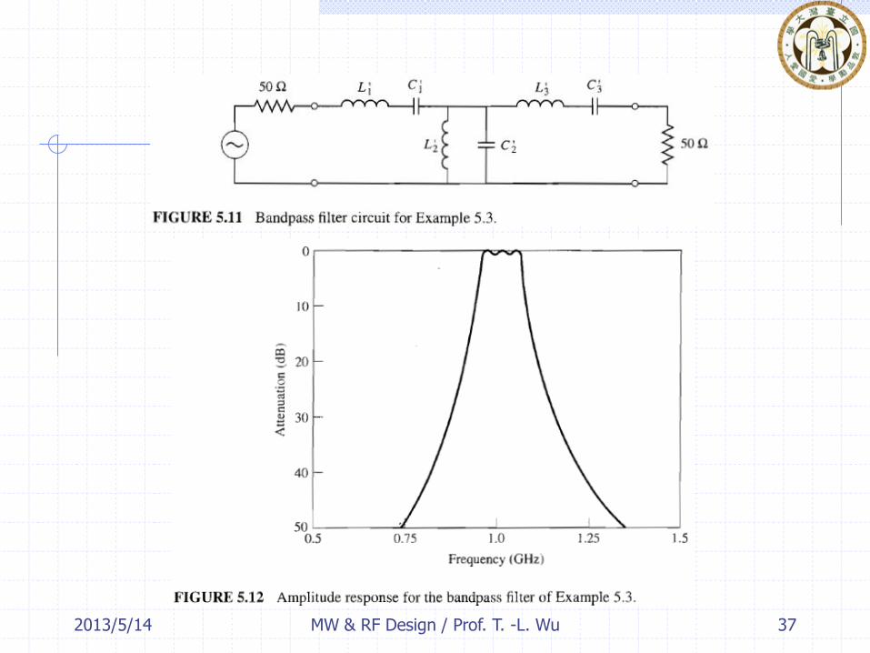
2013/5/14 37 MW & RF Design / Prof. T. -L. Wu

2013/5/14
5.3 Low pass and high pass filters using
transmission line stubs
The lumped-element filters discussed in the previous sections generally work well at low frequencies, but two problems arise at higher RF and microwave frequencies. First, lumped elements such as inductors and capacitors are generally available only for a limited range of values, and are difficult to implement at high frequencies.
In addition, at microwave frequencies the electrical distance between filter components is not negligible. Richard's transformation can be used to convert lumped elements to transmission line stubs. Kuroda's identities can be used to separate filter elements by using transmission line sections. Because such additional transmission line sections do not affect the filter response, this type of design is called redundant filter synthesis.
38 MW & RF Design / Prof. T. -L. Wu

2013/5/14
Richard’s Transformation
39 MW & RF Design / Prof. T. -L. Wu
This transformation was introduced by P. Richard to synthesize an LC network using open- and short-circuited transmission lines. if we replace the frequency variable ω with Ω, the reactance of an inductor can be written as and the susceptance of a capacitor can be written as

2013/5/14 40 MW & RF Design / Prof. T. -L. Wu
Cutoff occurs at unity frequency for a low-pass filter prototype; to obtain the same cutoff frequency for the Richard's-transformed filter,
Richard’s Transformation

2013/5/14 MW & RF Design / Prof. T. -L. Wu 41
Richard’s Transformation

2013/5/14
Kuroda Identities
42 MW & RF Design / Prof. T. -L. Wu
The four Kuroda identities use redundant transmission line sections to achieve a more practical microwave filter implementation by performing any of the following operations:
The additional transmission lines are called unit elements, and are λ /8 long at wc
The unit elements are thus commensurate with the stubs obtained by Richard's transform from the prototype design.

2013/5/14
Kuroda Identities
43 MW & RF Design / Prof. T. -L. Wu

2013/5/14
For Fig. 5.14(a)
44 MW & RF Design / Prof. T. -L. Wu
Prove identity (a)
Kuroda Identities

2013/5/14
For Fig. 5.14(b)
45 MW & RF Design / Prof. T. -L. Wu

2013/5/14 46 MW & RF Design / Prof. T. -L. Wu

2013/5/14 47 MW & RF Design / Prof. T. -L. Wu

2013/5/14 48 MW & RF Design / Prof. T. -L. Wu

2013/5/14 49 MW & RF Design / Prof. T. -L. Wu

2013/5/14 50 MW & RF Design / Prof. T. -L. Wu

2013/5/14
5.4 Stepped-impedance low-pass filter
51 MW & RF Design / Prof. T. -L. Wu
A relatively easy way to implement low-pass filters in microstrip or stripline form is to use alternating sections of very high and very low characteristic lines. Such filters are usually referred to a stepped-impedance. Popular because they are easy to design and take up less space than a similar low-pass filter using stubs. Because of the approximations involved, however, their electrical performance is often not as good as that of stub filters, so the use of such filters is usually limited to applications where a sharp cutoff is not required, such as for rejection of out-of-band mixer products.

2013/5/14 MW & RF Design / Prof. T. -L. Wu 52
Approximate Equivalent Circuits for Short Transmission Line Sections
The open-circuit impedance matrix elements for a transmission line of length l and characteristic impedance Zo can easily be found as
The series elements of a T-equivalent circuit for the transmission line section are then given as Zll - Z12 for the series arms, and Z12 for the shunt arm.

2013/5/14 53 MW & RF Design / Prof. T. -L. Wu
Approximate Equivalent Circuits for Short Transmission Line Sections

2013/5/14
Large Z0
Small Z0
54 MW & RF Design / Prof. T. -L. Wu
the actual values of Zh and Ze are usually set to the highest and lowest characteristic impedances that can be practically fabricated (the thinnest and widest lines, respectively). The lengths of the lines can then be determined from (5.39) and (5.40); to get the best response near cutoff, these lengths should be evaluated at w = wc
Combining the results of (5.39) and (5.40) with the impedance scaling equations of (5.15) allows the electrical lengths of the inductor sections to be calculated as

2013/5/14 55 MW & RF Design / Prof. T. -L. Wu

2013/5/14 56 MW & RF Design / Prof. T. -L. Wu

2013/5/14 57 MW & RF Design / Prof. T. -L. Wu

2013/5/14 58 MW & RF Design / Prof. T. -L. Wu

2013/5/14 MW & RF Design / Prof. T. -L. Wu 59
Bandpass filters perform a variety of critical functions in wireless systems, being used to reject out-of-band and image signals in the front end of a receiver, to attenuate undesired mixer products in transmitters and receivers, and to set the IF bandwidth of the receiver system. Impedance and Admittance Inverters Bandpass filter prototypes require shunt elements consisting of parallel LC resonators and series elements consisting of series LC resonators. Such an arrangement is very difficult to implement using transmission line sections, for which it is preferable to have either all shunt, or all series, elements. While the Kuroda identities are useful for transforming capacitors or inductors to either series or shunt transmission line stubs, they are not useful for transforming LC resonators. For this purpose, impedance (K) and admittance (J) inverters can be used. Such techniques are especially useful for bandpass and bandstop filters having narrow (t 10%) bandwidths.
5.5 BANDPASS FILTERS USING TRANSMlSSlON LINE RESONATORS

2013/5/14 MW & RF Design / Prof. T. -L. Wu 60
An impedance inverter converts a load impedance to its inverse, while an admittance inverter converts a load admittance to its inverse: where K is the impedance inverter constant, and J is the admittance inverter constant. They can be used to transform between series-connected and shunt-connected elements. Thus, a series LC resonator can be transformed to a parallel LC resonator, or vice versa.
Impedance and Admittance Inverters

2013/5/14 MW & RF Design / Prof. T. -L. Wu 61
In its simplest form, a K or J inverter can be constructed using a quarter-wave transformer of the appropriate characteristic impedance, Fig. (b) Others: T network (K inverter), or a pi network (J inverter), of capacitors. Fig. (c)
Impedance and Admittance Inverters

Practical Realization of Immittance Inverters
1 1 21 2
3 3
2
3 3
1 0
101
1
Z Z ZZ Z j L
Z Z
Zj L
Z Z
Z1
Z3
Z2
proof
+900 -900
+900 -900

Immittance inverters comprised of lumped and transmission line elements
A circuit mixed with lumped and transmission line elements

2013/5/14 MW & RF Design / Prof. T. -L. Wu 64
Since quarter-wave short-circuited transmission line stubs look like parallel resonant circuits, they can be used as the shunt parallel LC resonators for bandpass filters. Quarter wavelength connecting lines between the stubs will act as admittance inverters, effectively converting alternate shunt stubs to series resonators. For a narrow passband bandwidth (small Δ), the response of such a filter using N stubs is essentially the same as that of a lumped element bandpass filter of order N. The circuit topology of this filter is convenient in that only shunt stubs are used, but a disadvantage in practice is that the required characteristic impedances of the stub lines are often unrealistically low. A similar design employing open-circuited stubs can be used for bandstop filters
Bandpass Filters Using Quarter-Wave Coupled Quarter-Wave Resonators
How to design Z0n ?

2013/5/14 MW & RF Design / Prof. T. -L. Wu 65
Note that a given LC resonator has two degrees of freedom: L and C, or equivalently, ω0, and the slope of the admittance at resonance. For a stub resonator the corresponding degrees of freedom are the resonant length and characteristic impedance of the transmission line Z0n .
Bandpass Filters Using Quarter-Wave Coupled Quarter-Wave Resonators

2013/5/14 MW & RF Design / Prof. T. -L. Wu 66
Bandpass Filters Using Quarter-Wave Coupled Quarter-Wave Resonators

2013/5/14 MW & RF Design / Prof. T. -L. Wu 67
These two results are exactly equivalent for all frequencies if the following conditions are satisfied:

2013/5/14 MW & RF Design / Prof. T. -L. Wu 68

2013/5/14 MW & RF Design / Prof. T. -L. Wu 69

2013/5/14 MW & RF Design / Prof. T. -L. Wu 70

2013/5/14 MW & RF Design / Prof. T. -L. Wu 71

2013/5/14 MW & RF Design / Prof. T. -L. Wu 72
Bandpass Filters Using Capacitively Coupled Quarter-Wave Resonators
An Nth order filter will use N stubs, which are slightly shorter than λ/4 at the filter center frequency. The short-circuited stub resonators can be made from sections of coaxial line using ceramic materials having very high dielectric constant and low loss, resulting in a very compact design even at UHF frequencies [6]. Such filters are often referred to as ceramic resonator filters, and are presently the most common type of RF bandpass filter used in portable wireless systems.

2013/5/14 MW & RF Design / Prof. T. -L. Wu 73

Admittance inverter constant J – 2 order bandpass filter circuit
2013/5/14 MW & RF Design / Prof. T. -L. Wu 74
L2C2
J12
-90o
J01
-90o
J23
-90oL1
C1
R=ZoZo
Z2Zin
2223
3 23 o
o
JY J Z
Y
L2
C2
J12
-90o
J01
-90oL1
C1
Zo
Zin
Y3
2 2 32 2
2 12 12 2
1 1 1LYZ j C Y
Y J J j L
J01
-90o
L1
C1Zo
Z2
12 2
01 01 1 2
1 1 1 1Loadin
in
YZ j C
Y J J j L Z
YL

2013/5/14 MW & RF Design / Prof. T. -L. Wu 75
Equivalent L/C of Short-circuited stub : 4 o o
CZ
4 o
o
ZL
1
2
01
4 oo o
o
g ZZ
J
01
14oZ J
g
2
12
2
01 2
4 o o
o o
J Z Z
J g
12
1 24oZ J
g g
2
1232 2
01 23
1o
o
Jg Z
G J J Z
23
2 34oZ J
g g
The two results are exactly equivalent for all frequencies :
J01
-90o
L1
C1Zo
12 2
01 01 1 2
1 1 1Loadin
YZ j C
J J j L Z
2
1 01C J 2
01 1J L
2
1222
01
JL
J
2
0122
12
JC
J
2201232
12
o
JG J Z
J
1 o
o
g Z
1 o og Z
2
o
o
Z
g
2
o o
g
Z
3 oR g Z
Lowpass to Bandpasstransformation
1g
2g 3g

Bandpass filter structure
π-network of J-inverter
Circuit implementation
π-network for realizing BPF
2013/5/14 MW & RF Design / Prof. T. -L. Wu 76
L2C1 C2J12J01 L1 LN CN JN, N+1
L2C1 C2L1 LN CN-C01 -C01
C01
-C12 -C12
C12
-CN, N+1
CN, N+1
-CN, N+1
How to deal with the J-inverter at the two ends due to the negative capacitors next to the terminations?
C
-C
J-inverter
-C
J=ωC

The coupling capacitor values at input/output end for matching (I) BPF circuit with admittance inverter BPF circuit with capacitor circuit
2013/5/14 MW & RF Design / Prof. T. -L. Wu 77
Equating G to the real part of Y :
2
2 0
01 2
01
o x
o
o x
Z CJ Z
Z C
2 22 2
01 0 1x x oJ C J Z
010 22
011x
o
JC
J Z
220101 o
L
JG J Z
Y
00 0
0
0
2
0 0
0 2
0
2
0 002 2
0 0
1
1 1
1
1 1
xy y
o xo
x
x o x
y
o x
o x xy
o x o x
j CY j C j C
jZ CZj C
j C Z Cj C
Z C
Z C j Cj C G jB
Z C Z C
J01 L1 C1ZoL1 C1Zo Cy
Cx

The coupling capacitor values at input/output end for matching (II)
2013/5/14 MW & RF Design / Prof. T. -L. Wu 78
The imaginary part of Y should be eliminated:
2
0 002 2
0 01 1
o x xy
o x o x
Z C j CY j C G jB
Z C Z C
0
02
0
01
xy
o x
j Cj C
Z C
2
01
xy
o x
CC
Z C
Note: In additional to the modified coupled capacitor Cx, the shunt capacitor Cy is also revised. The Cy is
not directly equal to the Cx unless ω0Cx << 1 and this is the assumption in the textbook.
Textbook
Accurate
L2C1 C2L1 LN CN-C01
C01
-C12 -C12
C12CN, N+1
-CN, N+1
L2C1 C2L1 LN CN-C’01
C01
-C12 -C12
C12CN, N+1
-C’N, N+1
' 0101 2
011 o
CC
Z C

2013/5/14 MW & RF Design / Prof. T. -L. Wu 79
Trick for the final circuit for implementing the BPF

Difference on the two circuits
2013/5/14 MW & RF Design / Prof. T. -L. Wu 80
Accurate
Ideal
Third order BPF with 0.5 dB Chebyshev prototype
g1 = 1.5963, g2 = 1.0967, g3 = 1.5963, g4 = 1
f0 = 1 GHz, FBW = 5 %, Zo = 50
LC CJ12J01 L L C J34J23
LC CL L C
C01
-C12
C12 C34
-C23
C23
-C’01 -C’
34
0.9 0.95 1 1.05 1.1
Freq(GHz)
-40
-30
-20
-10
0
S-p
ara
mete
r (d
B)
0 0.1 0.2 0.3 0.4 0.5 0.6 0.7 0.8 0.9 1
u=2/(1+2)
2.2
2.4
2.6
2.8
3
3.2
3.4
3.6
3.8
4
f 3/f
1
Ideal
Textbook
0.9 0.95 1 1.05 1.1
Freq(GHz)
-40
-30
-20
-10
0
S-p
ara
mete
r (d
B)
0 0.1 0.2 0.3 0.4 0.5 0.6 0.7 0.8 0.9 1
u=2/(1+2)
2.2
2.4
2.6
2.8
3
3.2
3.4
3.6
3.8
4
f 3/f
1
Ideal
Accurate

2013/5/14 MW & RF Design / Prof. T. -L. Wu 81
The transformation of the stub length to account for the change in capacitance is illustrated in Figure 5.25d. A short-circuited length of line with a shunt capacitor at its input has an input admittance of

2013/5/14 MW & RF Design / Prof. T. -L. Wu 82
Dielectric material properties play a critical role in the performance of dielectric resonator filters. Materials with high dielectric constants are required in order to provide miniaturization at the frequencies typically used for wireless applications. Losses must be low to provide resonators with high Q, leading to low passband insertion loss and maximum attenuation in the stopbands. And the dielectric constant must be stable with changes in temperature to avoid drifting of the filter passband over normal operating conditions. Most materials that are commonly used in dielectric resonator filters are ceramics such as Barium tetratitanate, Zinc/Strontium titanate, and various titanium oxide compounds.

2013/5/14 MW & RF Design / Prof. T. -L. Wu 83

2013/5/14 MW & RF Design / Prof. T. -L. Wu 84

2013/5/14 MW & RF Design / Prof. T. -L. Wu 85