
Filter CS Final
62
Dr. Chinmoy Saha Indian Institute of Space Science and Technology Dr. Chinmoy Saha Indian Institute of Space Science and Technology Microwave Filter Design : Insertion Loss Method Microwave Filter Design : Insertion Loss Method
-
Upload
dhanya-rao-mamidi -
Category
Documents
-
view
222 -
download
0
Transcript of Filter CS Final

Dr. Chinmoy Saha
Indian Institute of Space Science and Technology
Dr. Chinmoy Saha
Indian Institute of Space Science and Technology
Microwave Filter Design : Insertion Loss Method
Microwave Filter Design : Insertion Loss Method

IntroductionIntroduction
A filter is a network that provides perfect transmission for signal withfrequencies in certain passband region and infinite attenuation in the stopband-regions.Such ideal characteristics cannot be attained, and the goal of filter design isto approximate the ideal requirements to within an acceptable tolerance.
w
ww
1
2
V
VH =
=
w
w
1
21020
V
VLognAttenuatio
A FilterH(w)
V1(w) V2(w)
Transfer Function

Filters are used in all frequency ranges and are categorized intothree main groups:•Low-pass filter (LPF) that transmit all signals between DC andsome upper limit wc and attenuate all signals with frequenciesabove wc.
•High-pass filter (HPF) that pass all signal with frequenciesabove the cutoff value wc and reject signal with frequenciesbelow wc.
•Band-pass filter (BPF) that passes signal with frequencies inthe range of w1 to w2 and reject frequencies outside this range.The complement to band-pass filter is the band-reject or band-stop filter.
w
Attenuation/dB
0
wc
3
10
20
30
40
w
Attenuation/dB
0
w1
3
10
20
30
40 w2
Attenuation/dB
w
0
wc
3
10
20
30
40
ClassificationsClassifications

L1=g2 L2=g4
C1=g1 C2=g3RL= gN+1
1
L1=g1 L2=g3
C1=g2 C2=g4RL= gN+1g0= 1
L2L1
C1 CN
C2L2
L1C1 L3
C3
CNLN
high-pass filter
Low -pass filter
band-pass filter
ClassificationsClassifications

Filter can be further divided into active and passive type.For passive filter output power <= input powerActive filter provides power gain. Some amplifying Stage(Normally OPAMP) must be there.The characteristic of a passive filter can be described usingthe transfer function approach or the attenuation functionapproach.In low frequency circuit the transfer function (H(w))description is usedAt microwave frequency the attenuation function descriptionis preferred.At frequency below 1.0GHz, filters are usually implementedusing lumped elements such as resistors, inductors andcapacitors.
ClassificationsClassifications

Filter Characterization
Two-port Network
H(w)Input Output
Fig. 1 Two-port Network
)()()( www jeHH =

Filter Characterization
Fig. 2 Characteristics of
ideal bandpass filter
1
Freq.
lH(w)l
(w)
Characteristics of ideal bandpass filters ;
>
=
21
21
, 0
1)(
fffffor
fffforH w dand ww =)(
→ not realizable→ approximation required

Filter Characterization :Filter Characterization : Practical specificationsPractical specifications
Passband : Lower cutoff frequency f1 and upper cutoff frequency f2
Insertion loss: , must be as small as possible
Return Loss: , degree of impedance matching
Ripple: variation of insertion loss within the passband
Phase Delay and Group Delay: are measures of the amount of delay encountered by a signal as it passes through a network.
Group delay describes the delay of a packet of frequencies
Phase delay describes the delay for a single sinusoid.is the phase of H(w) in radians.
Skirt frequency characteristics :depends on the system specifications
Power handling capability
)( )(log20 dBH w
)( log20 dB
w
w
d
dd
)(=
w
w
)(=P
)(w

There are essentially two Synthesis Techniques at low-frequency : a) Image parameter Method (IPM)b) Insertion-Loss Method (ILM)
Filter Syntheses TechniquesFilter Syntheses Techniques
Image parameter Method (IPM) Provides a relatively simple filter design approachThe IPM approach divides a filter into a cascade of two-port networks, and attempt to come up with the schematic of each two-port, such that when combined, give the required frequency response. Arbitrary frequency response cannot be incorporated into the design
m=0.6 m=0.6m-derivedm<0.6
constantkT
2
1
2
1
Matchingsection
Matchingsection
High-fcutoff
Sharpcutoff
ZiTZ
iT ZiT
ZoZo

A filter response is defined by its insertion loss or power loss ratio (PLR)
Then a suitable filter schematic is synthesized.
Design procedure is based on the attenuation response or insertion loss of the filter.
Allows a high degree of control over the pass band and stop band amplitude and phase characteristics, with a systematic way to synthesize a desired response.
The necessary design trade-offs can be evaluated to best meet the application requirements.
Out of lot of Choices (Butterworth, Chebyshev, Elliptic Function, Linear Phase etc.) are there to the designers. Based on the design specification and constrain an optimum design is to be chosen.
Insertion-Loss Method (ILM) Insertion-Loss Method (ILM)
if a minimum insertion loss is most important, a binomial response can be used
if a sharp cutoff is needed, a Chebyshev response is better
in the insertion loss method a filter response is defined by its insertion loss or power loss ratio

Insertion Loss MethodInsertion Loss Method
It begins with a complete specification of a physically realizable frequency characteristic
Normally the design starts with a normalized low-pass prototype (LPP). The LPP is a low-pass filter with source and load resistance of 1W and cutoff frequency of 1 Radian/s.
Impedance transformation and frequency scaling are then applied to denormalize the LPP and synthesize different type of filters with different cutoff frequencies.
There are a number of standard approaches to design a normalized LPP that approximate an ideal low-pass filter response with cutoff frequency of unity.
well known methods are:Maximally flat or Butterworth function.Equal ripple or Chebyshev approach.Elliptic function.

Power Loss Ratio (PLR)
[Sij]
Pin
Prefl
Ptrans
is an even function of w , so
inintrans
ininrefl
PSPTP
PSPP
2
21
2
2
11
2
==
==
2)(1
1
w=
tran
inLR
P
PP
Filter Design :Insertion Loss MethodFilter Design :Insertion Loss Method
IL = 10 log PLR
)()(
)()(
22
22
ww
ww
NM
M
=
2)(w
← network synthesis procedures are required
)(
)(1
1
12 w
w
D
N
P
PP
tran
inLR =
=
M (w2) and N (w2) are real polynomials

Type of responses for n-section prototype filter
A. Maximally flat response (Butterworth Response)
The pass band extends from w = 0 to w = wc
At the band edge the power loss ratio is 1 + k2.
For this point to be -3 dB point, we have k = 1.
N
c
LR kP
2
21
=
w
w
Provides the flattest possible passband response for a given filter complexity, or order. For a low-pass filter, it is specified by
k2 :passband tolerance
N:order of filter
N
c
LR kP
2
2
w
wFor w >>wc
So the insertion loss increases at the rate of 20N dB/decade
21 k
For N = 3

B. Equal ripple response (Chebyshev Response)
Type of responses for n-section prototype filter
TN (x) Chebyshev Polynomial of order NOscillates between -1 to +1 for
)()(2)(
34)( ,12 ,)(
21
33
221
xTxxTxT
xxxTxTxxT
nnn =
===
1x
For N = 3
=
0
221w
wNLR TkP
For large x,So for w>>wc insertion loss
Nn xxT )2(
2
1)( =
N
c
LR
kP
22 2
4
w
w Insertion loss increases at the
rate of 20N dB/decade
Sharper cut-off compared to Butterworth Passband response contain ripples of amplitude 1+k2
For w>>wc, Insertion loss is times greater than Butterworth filter( ) /2 42N

C. Elliptic Function
Type of responses for n-section prototype filter
It has equal-ripple responses in both passband and stopband
Maximum attenuation in the passband is Amax
Minimum attenuation in the stopband is Amin
are difficult to synthesize

linear phase response is necessary to avoid signal distortion
there is usually a tradeoff between the sharp-cutoff response
and linear phase response
a linear phase characteristic can be achieved with the phase
response
=
N
c
pA
2
1)(w
www
D. Linear Phase Response
Type of responses for n-section prototype filter
The group delay is given by
this is also a maximally flat function, therefore, signal distortion is
reduced in the passband
==
N
c
d NpAd
d2
)12(1w
w
w

We start with designing the low pass filter prototypes which are
normalized in terms of impedance and frequency
The designed prototypes are then scaled in frequency and impedance
Lumped-elements will be replaced by distributive elements for
microwave frequency operations
Design Steps
Filter Specifications
Low PassPrototype Design
Scaling and Conversion
Implementation

Maximally Flat Low Pass Filter Prototype (Butterworth)
we will derive the normalized element values, L and C, for a maximally flat response. Assume : source impedance of 1 Ω
Cut off frequency wc = 1The desired power loss ratio (k =1) with N= 2 is
Consider the two-element (N=2) low-pass filter prototype shown
41 w=LRP
Input impedance2221
)1(
1 CR
RCjRLj
RCj
RLjZin
w
ww
ww
=
=

Reflection Co-efficient is given by
1
1
=
in
in
Z
Z
The power loss ratio is given by
Maximally Flat LPF Prototype (Butterworth)… Contd

This expression is a polynomial in ω2
Comparing to the desired response R =1, since PLR=1 for ω=0.
In addition, the coefficient of ω2 must vanish
coefficient of ω4 to be unity
Specification
Maximally Flat LPF Prototype (Butterworth)… Maximally Flat LPF Prototype (Butterworth)… ContdContd
41 w=LRP

This procedure can be extended to find the element values for higher N (?)Not practical for large value of N. The element values for the ladder-type circuits is tabulated . (for normalized low-pass design, source impedance is 1 and ωc =1 rad/sec)
N= 3 , 4 , 5 , 6 , 7 , 8 , 9 , 10 , . . .N= 3 , 4 , 5 , 6 , 7 , 8 , 9 , 10 , . . .
((bb))
((aa))

N= 3 , 4 , 5 , 6 , 7 , 8 , 9 , 10 , . . . …N= 3 , 4 , 5 , 6 , 7 , 8 , 9 , 10 , . . . …ContdContd

Element Values for Maximally Flat LPF PrototypesElement Values for Maximally Flat LPF Prototypes
(g0 =1, ωc =1, N =1 to 10)
G. L. Matthaei, L. Young, and E. M. T. Jones,Microwave Filters, Impedance-Matching Networks, and Coupling Structures, Artech House, Dedham, Mass., 1980
),( , 2, 1, ,2
12sin2 FHNi
N
igi =
=

Performance with higher NPerformance with higher N
Attenuation versus normalized frequency for maximally flat filter prototypes

Equal Ripple Low Pass Filter Prototype (Chebyshev)
For an equal-ripple low-pass filter with a cutoff frequency ωc =1 rad/sec, the power loss ratio
where 1+k2 is the ripple level in the passband.
Since the Chebyshev polynomials have the property that
At ω = 0
=
21
1
kPLR
=1
0)0(NT For N odd
For N even
For N oddFor N even
)(1 22 wNLR TkP =
There are two cases to consider, depending on N odd or even

Consider the two-element (N=2) low-pass filter prototype shown
Low pass prototype for Low pass prototype for N = N = 22
22222
2 )12(1)(1 == ww kTkPLR
)144(1 242 = wwk ()(
,12 22
TxxT
xT
=
Can be solved for R,L, and C if the ripple level (determined by k2) is specified
= )144(1 242 wwk
Equating
Equating at ω =0 R
Rk
4
12
2 =

Equating the coefficients ofω2 and ω4
2222
4
14 RCL
Rk =
)2(4
14 22222 LCRLCR
Rk =
can be used to find L and C
R is not unity leading to impedance mismatch if the load is unity.
Solutions : quarter wave transformerAdd an additional filter element to make N odd
22 1221 kkkR = (For N even)
= )144(1 242 wwk
Low pass prototype for Low pass prototype for N = N = 2 ….2 ….ContdContd

Element Values for EqualElement Values for Equal--Ripple LPF Prototypes (Ripple LPF Prototypes (gg0 0 = 1,= 1,ωωc c = 1, = 1, NN=1 to 10)=1 to 10)
0.5 dB ripple 1+k2 = 10^(0.5/10)=1.122
For odd N , gN+1=1, Impedance Matched
For even N, gN+1 = 1.9841

Element Values for EqualElement Values for Equal--Ripple LPF Prototypes (Ripple LPF Prototypes (gg0 0 = 1,= 1,ωωc c = 1, = 1, NN=1 to 10)=1 to 10)
3 dB ripple 1+k2 = 10^(3/10)=2
For odd N , gN+1=1, Impedance Matched
For even N, gN+1 = 5.8095

11
14
=ii
iii
gb
aag
N
i
Nbi
b 22 sin2
sinh =
=
11
11ln
2
2
k
kb
N
ag
2sinh
2 11 b
=
N
iai
2
12sin
=
Parameter ExtractionParameter Extraction
11010 =IL
k

0.5 dB Ripple Level
Attenuation Attenuation vsvs Normalized FrequencyNormalized Frequency

3 dB Ripple Level
Attenuation Attenuation vsvs Normalized FrequencyNormalized Frequency

Filters having a maximally flat time delay, or a linear phase response, can be designed inthe same way, but things are somewhat more complicated because the phase of the voltage transfer function is not as simply expressed as is its amplitude. Design values have
Linear Phase LowLinear Phase Low--Pass Filter PrototypesPass Filter Prototypes
been derived for such filters [1], however, again for the ladder circuits of Figure 8.25, and they are given in Table 8.5 for a normalized source impedance and cutoff frequency (ωc =1rad/sec). The resulting normalized group delay in the passband will be τd = 1/ωc =1 sec.

Filter TransformationFilter Transformation
For the LPF prototypes discussed so far we had Rs =1Ω and cutoff frequency ωc =1 rad/sec. So we need impedance and frequency scaling .Also, conversion mechanism to get high-pass, bandpass, or bandstop characteristics.
LL
S
RRR
RR
R
CC
LRL
0
0
0
0
=
=
=
=
Impedance Scaling
Illustration (Impedance level × 50)
same reflection coefficient maintained
Series branch(impedance) elements
Shunt branch(admittance) elements ;
W=W= 50 1 LL RR
iiii gggjgj 5050 ww
50/50/ rrrr gggjgj ww

Series Reactance
Filter Transformation: Filter Transformation: Frequency Scaling (LPF to LPF)
To change the cutoff frequency of a low-pass prototype from unity to ωc we replace ω by ω/ωc
kK
c
k LjLjjX == ww
w
cw
ww
Shunt Susceptance
kK
c
k CjCjjB == ww
w
So the new element values are
c
kk
CC
w=
c
kK
LL
w=
If both impedance and frequency scaling is required
c
kk
R
CC
w0
=
c
kK
LRL
w0=
Frequency scaling for low-pass filters

Series Reactance
Filter Transformation: Filter Transformation: (LPF to HPF)
k
Kc
kCj
LjjX
==ww
w 1
w
ww c
Shunt Susceptance
So the new element values are
kc
kC
Lw
1=
kc
kL
Cw
1=
If both impedance and frequency scaling is required
Transformation of a LPF into HPF
k
kc
kLj
CjjB
==ww
w 1
kc
kLR
Cw0
1=
kc
kC
RL
w0=

Low-pass prototypes can also be transformed to have the bandpass or bandstop responses.
BandpassBandpass and and BandstopBandstop TransformationsTransformations
LPFBPF:
Where ω1 and ω2 denote the edges of the passband,
LPF BPF BSF

Series reactance
Shunt Susceptance
LPF to BPFLPF to BPF

LPF to BSFLPF to BSF
LPFBSF:
=
=
w
w
w
w
w
w
w
w k
k
kk
L
L
jLjjX
0
0
0
0
So the series inductors of the low-pass prototype are converted to parallel LC circuits with
Similarly the shunt capacitors is changed to

Summary of Prototype Filter TransformationSummary of Prototype Filter Transformation

Design Problem 1:Design Problem 1: Calculate the inductance and capacitance values for a maximally-flat low-pass filter that has a 3dB bandwidth of 400MHz. The filter is to be connected to 50 ohm source and load impedance. The filter must has a high attenuation of 20 dB at 1 GHz.
=
n
kgk
2
12sin2
Step 1: Determine the order of the filter
c
A
Nww /log2
110log
110
10/10
=
=
N
c
A
2
11log10w
w
2
400/1000log2
110log
10
10/2010 >
=
Thus choose an integer value , i.e N=3
Step 2: Determine the element values (If not supplied)

1
32
12sin21 =
=
gg0 = g 3+1 = 1
2
32
122sin22 =
=
g
1
32
132sin23 =
=
g
Step 2: Determine the element values (If not supplied) ….
nHgR
LLc
o 9.19104002
1506
113 =
===
w
pFR
gC
co
9.1510400250
26
22 =
==
w
Step 3: Transformation for Scaling
15.9pF
19.9nH
50 ohm
50 ohm 19.9nH
Step 3: Circuit
nHgR
Lc
o 8.39104002
2506
22 =
==
w
pFR
gCC
co
95.710400250
16
113 =
===
w
7.95pF
39.8nH
50 ohm
50 ohm
7.95pF

Design Problem 2 :Design Problem 2 : Design a maximally flat low-pass filter with a cutoff frequency of 2 GHz, impedance of 50 Ω, and at least 15 dB insertion loss at 3 GHz.
=
n
kgk
2
12sin2
Step 1: Determine the order of the filter
c
A
Nww /log2
110log
110
10/10
=
=
N
c
A
2
11log10w
w
42/3log2
110log
10
10/1510 >
=
Thus choose an integer value , i.e N=5
Step 2: Determine the element values (If not supplied)
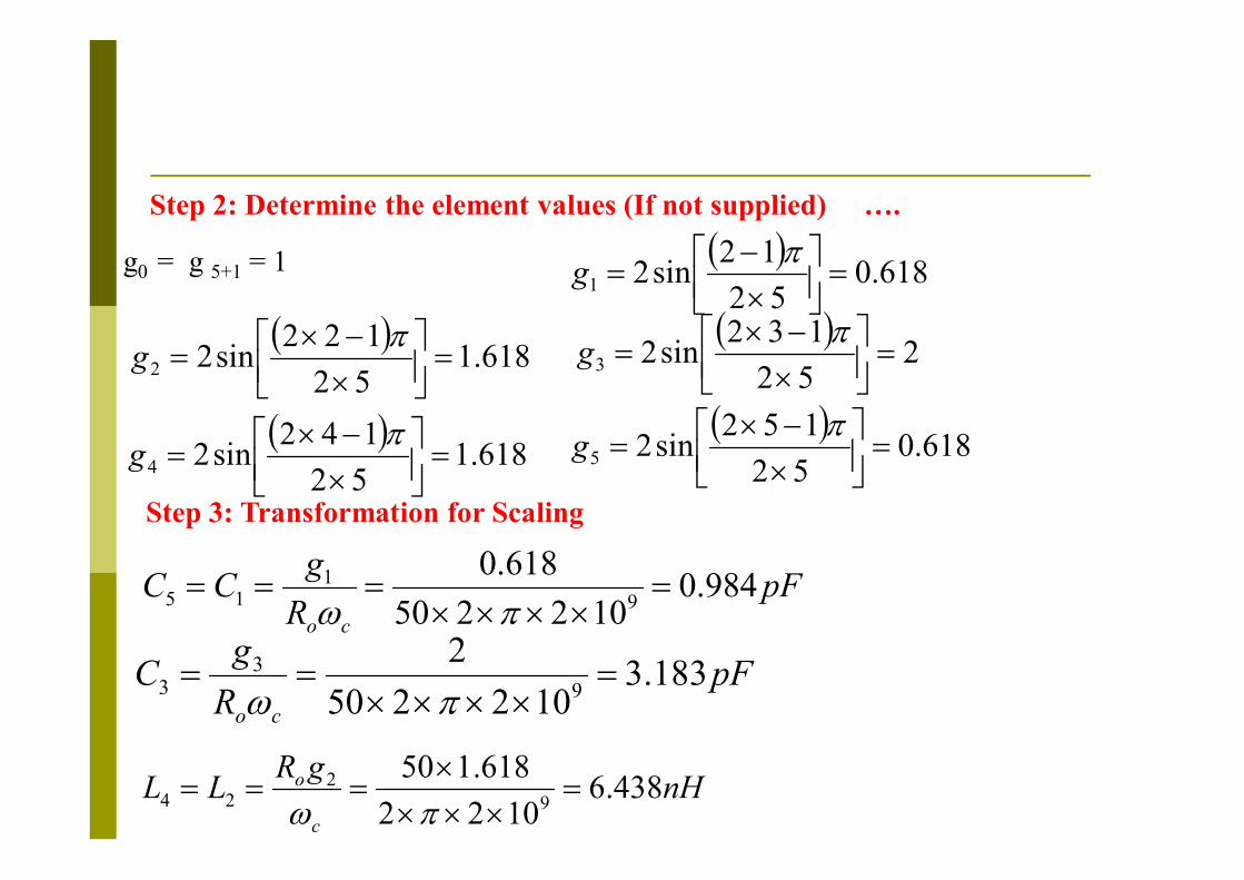
618.0
52
12sin21 =
=
gg0 = g 5+1 = 1
618.1
52
122sin22 =
=
g
2
52
132sin23 =
=
g
Step 2: Determine the element values (If not supplied) ….
618.1
52
142sin24 =
=
g
618.0
52
152sin25 =
=
g
pFR
gCC
co
984.0102250
618.09
115 =
===
w
nHgR
LLc
o 438.61022
618.1509
224 =
===
w
pFR
gC
co
183.3102250
29
33 =
==
w
Step 3: Transformation for Scaling

Step 3: Circuit
Alternatively you can go for other type .

Design Problem 3Design Problem 3Design a bandpass filter having a 0.5 dB equal-ripple response, with N=3. The center frequency is 1 GHz, the bandwidth is 10%, and the impedance is 50.
From TableImpedance and Frequency Transformation
BPF Circuit

Design Problem 3Design Problem 3
Design a 3 section Chebyshev low-pass filter that has a ripple of 0.05dB and cutoff frequency of 1 GHz.
11
14
=ii
iii
gb
aag
N
i
Nbi
b 22 sin2
sinh =
=
11
11ln
2
2
k
kb
N
ag
2sinh
2 11 b
=
N
iai
2
12sin
=
11010 =IL
k
Extraction EquationsExtraction Equations
k = 0.1076078715 b= -5.850582044 137134.12
sinh =N
b
29307.12
sinh 2 =N
b
879.0137134.1
2
12
1 =
=g 1132.14
11
212 ==
gb
aag
879.04
22
323 ==
gb
aag nHLL 7
102
8794.050931 =
==
pFC 543.3
10250
1132.192 =
=

48
Design Problem 4Design Problem 4Design a band-pass filter having a 0.5 dB ripple response, with N=3. The center frequency is 1GHz, the bandwidth is 10%, and the impedance is 50W.
Solution
Extract the Parameters
go=1 , g1=1.5963, g2=1.0967, g3= 1.5963, g4= 1.000
Let’s first and third elements are equivalent to series inductance and g1=g3, thus
nHgZ
LLo
oss 127
1021.0
5963.1509
131 =
=
W==
w
pFgZ
CCoo
ss 199.05963.150102
1.09
131 =
=
W==
w
kok gZL =

Continue
49
Second element is equivalent to parallel capacitance, thus
nHg
ZL
o
op 726.0
0967.1102
501.09
22 =
=
W=
w
pFZ
gC
oop 91.34
1021.050
0967.19
22 =
=
W=
w
o
kk
Z
gC =
50W 127nH 0.199pF
0.726nH 34.91pF
127nH 0.199pF
50W

MicrostripMicrostrip Implementation : Why ?Implementation : Why ?
The lumped-element filter sections generally work well at low frequencies only.At higher RF and microwave frequencies lumped-element inductors and capacitors are not available (Available only for a limited range of values), and can be difficult to implement at microwave frequencies. Distributed elements such as open-circuited or short-circuited transmission line stubs, are often used to approximate ideal lumped elements.At microwave frequencies the distances between filter components is not negligible. (Additional Challenge)

Lumped elements can be converted to transmission linesections with Richards’ transformation.
Kuroda’s identities is used to physically separate filterelements by using transmission line sections.
Such additional transmission line sections do not affect the filterresponse, this type of design is called redundant filter synthesis.
It is possible to design microwave filters that take advantage ofthese sections to improve the filter response.
MicrostripMicrostrip Implementation : HowImplementation : How

Implementation using stub
Richard’s transformation
==W
pv
lwb tantan
btanjCCjjBc =W=
At cutoff unity frequency we have Ω =1. Then
btan1 ==W8
l=
So inductor and capacitors of the lumped –element circuit are replaced by shorted and open stub of length l/8 at wc.
btanjLLjjX L =W=
Transformation from Ω plane to w plane
Reactance of the inductor is
Susceptance of the capacitor is
An inductor can be replaced with a short-circuited stub of length bl and characteristic impedance LA capacitor can be replaced with an open-circuited stub of length βl and characteristic impedance 1/C

Richard’s transformation : Summary

The four Kuroda identities use redundant transmission line sections to achievea more practical microwave filter implementation. Physically separate transmission line stubs.
For that additional transmission lines are addedTransform series stubs into shunt stubs, or vice versaChange impractical characteristic impedances into more realizable values
Kuroda’s IdentitiesKuroda’s Identities

The Four Kuroda Identities(n2=1+Z2/Z1)
It is difficult toimplement aseries stub inmicrostripline.Using Kurodaidentity, wewould be ableto transformS.C series stubto O.C shuntstub. So the 2nd
identity is mostcrucial.

Kuroda identity :Proof1st identity

ABCD of the shunt stub
W=
=
1
01
1
01
2. Z
jYDC
BA
StubSt
ABCD of the Tr. Line of length l stub
W
W
W
W=
1
1
1
11
01
1
1
2
2 Z
jZj
Z
jDC
BA
lbtan=Wwhere
So the combined ABCD (LHS)
W
W
W
W=
2
12
21
1
2 111
1
1
1
Z
Z
ZZj
Zj
W
W
W=
=
1
1
1
1cossin
sincos
1
1
2
1
1
Z
jZj
llZ
jljZl
DC
BA
TLbb
bb
22 cot
1
Z
j
ljZY
W==
b
(1)
Kuroda identity :Proof

ABCD of the series stub
W=
=
10
1
10
12
1
.
n
ZjZ
DC
BA
StubSer
ABCD of the Tr. Line of length l
W
W
W
W=
10
1
1
1
1
12
1
2
2
22
2 n
Zj
Z
njn
Zj
DC
BA
lbtan=W
where
So the combined ABCD (RHS)
WW
W
W=
2
12
2
2
212
21
)(1
1
1
Z
Z
Z
nj
ZZn
j
W
W
W=
1
1
1
1
2
2
22
2
Z
njn
Zj
DC
BA
TL
(2)
From (1) and (2), LHS and RHS are identical if
1
22 1Z
Zn =
Kuroda identity :Proof
Other Kuroda identities can be proved in a similar fashion

Second Kuroda’s Identity
Consider the second identity in which a series stub is converted into a shunt
l/8
l/8
Z1
Zo
Z1+Zo
Zo+Zo
2/Z1
SC
OC

From Table g1= 0.7654 g2 = 1.8478 g3=1.8478
g4 = 0.7654 g5 = 1
Design Problem 5 :Design a low-pass third-order maximally flat filter using only shunt stubs. The cutoff frequency is 8GHz and the impedance is 50 W.
LPF prototype
0.765 1.848
1/1.848
=0.541 1/0.765=1.307
Applying Richard’s transformation Adding Elements

Use second Kuroda identity on left,
Use first Kuroda identity on right433.0
307.2
1
307.1
1
)1307.1
11(
122 ==
=n
Z
567.0307.2
307.11
)1307.1
11(
121 ==
=n
Z
307.21)765.0
11(
765.1765.0)765.0
11(
22
12
==
==
Zn
Zn
1.765
1.848
0.541
0.433
11
2.307
0.567Use second Kuroda identity on left,
741.0567.0)848.1
567.01(
415.2848.1)848.1
567.01(
22
12
==
==
Zn
Zn
Use second Kuroda identity on left,
309.31)433.0
11(
433.1433.0)433.0
11(
22
12
==
==
Zn
Zn
1.765
0.541
11
2.307
2.415 1.433
0.741 3.309
Apply Kuroda’s identity…..

all lines are l/8 long at 8 GHz
88.3
27.1
5050
115.4
120.8 71.7
37.1 165.5
Impedance ScalingImpedance Scaling
All elements are multiplied by 50
Microstrip implementation
5088.3 120.8 71.7
50
115.4 27.1 37.1 165.5
ii/p/p o/po/p
er