Film Capacitors - Metallized Polypropylene Film Capacitors ...Metallized polypropylene film...
30
Film Capacitors Metallized Polypropylene Film Capacitors (MKP) Series/Type: B32620, B32621 Date: June 2018 © EPCOS AG 2018. Reproduction, publication and dissemination of this publication, enclosures hereto and the information contained therein without EPCOS' prior express consent is prohibited. EPCOS AG is a TDK Group Company.
Transcript of Film Capacitors - Metallized Polypropylene Film Capacitors ...Metallized polypropylene film...
Film Capacitors
Metallized Polypropylene Film Capacitors (MKP)
Series/Type: B32620, B32621
Date: June 2018
© EPCOS AG 2018. Reproduction, publication and dissemination of this publication, enclosures hereto and theinformation contained therein without EPCOS' prior express consent is prohibited.
EPCOS AG is a TDK Group Company.

Typical applicationsCompact fluorescent lamps (CFL)SMPS
ClimaticMax. operating temperature: 105 °CClimatic category (IEC 60068-1:2013):55/100/56
ConstructionDielectric: polypropylene (PP)Stacked-film technologyPlastic case (UL 94 V-0)Epoxy resin sealing
FeaturesVery high pulse strengthVery good self-healing propertiesSmallest possible dimensionsHigh contact reliabilityRoHS-compatible
TerminalsParallel wire leads, lead-free tinnedSpecial lead lengths available on request
MarkingManufacturer's logo,rated capacitance (coded),cap. tolerance (code letter), rated voltage,date of manufacture (coded),for lead spacing 7.5 mm: style (MKP),for lead spacing 10 mm: lot number, series number (621)
Delivery modeBulk (untaped)Taped (Ammo pack or reel)For notes on taping, refer to chapter "Taping and packing“.
Dimensional drawing
Dimensions in mm
Lead spacing±0.4
Lead diameterd1 ±0.05
Type
1) 0.5 mm for capacitor width w = 4 mm
7.5 0.5 B32620
10.0 0.61) B32621
Metallized polypropylene film capacitors (MKP) B32620, B32621
High pulse (stacked)
Page 2 of 30Please read Cautions and warnings andImportant notes at the end of this document.
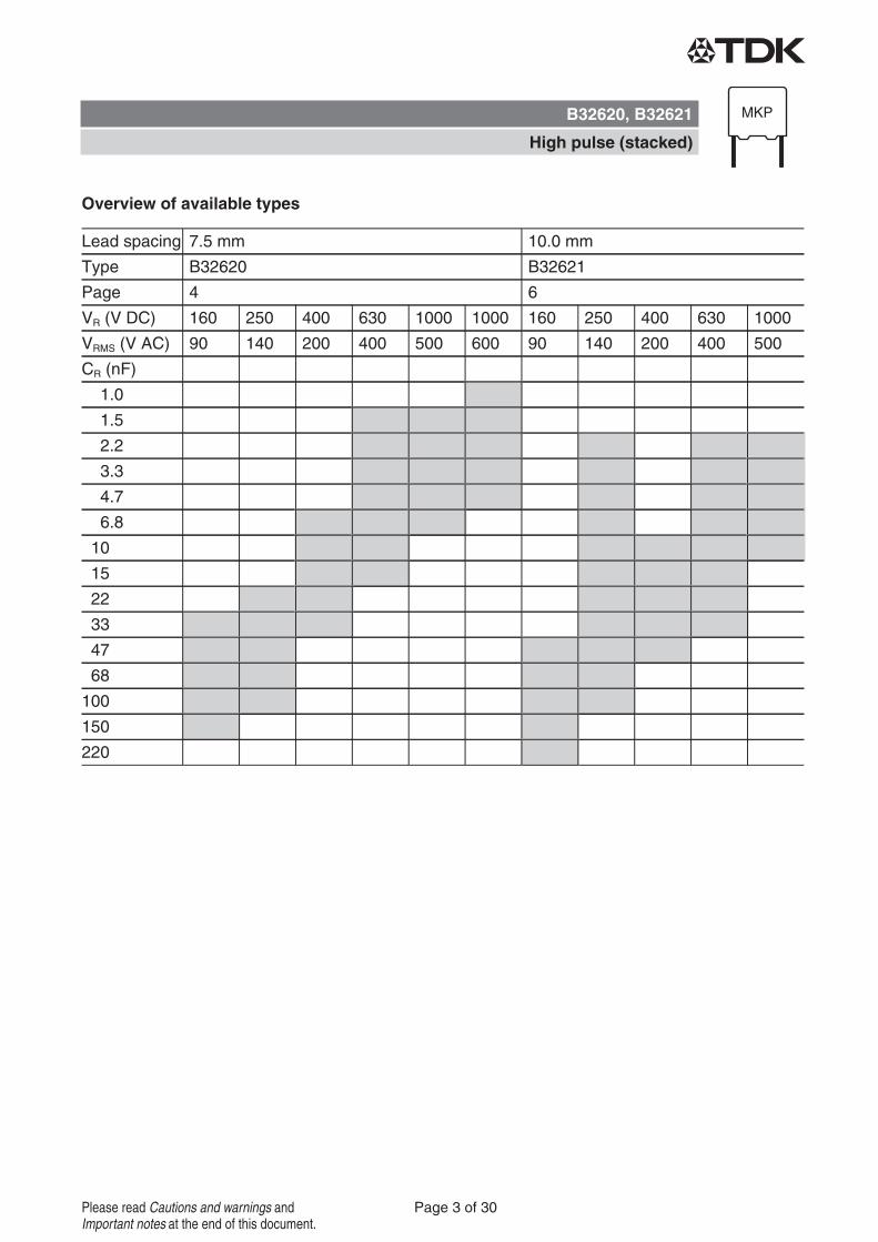
Overview of available types
Lead spacing 7.5 mm 10.0 mm
Type B32620 B32621
Page 4 6
VR (V DC) 160 250 400 630 1000 1000 160 250 400 630 1000
VRMS (V AC) 90 140 200 400 500 600 90 140 200 400 500
CR (nF)
1.0
1.5
2.2
3.3
4.7
6.8
10
15
22
33
47
68
100
150
220
B32620, B32621
High pulse (stacked)
Page 3 of 30Please read Cautions and warnings andImportant notes at the end of this document.
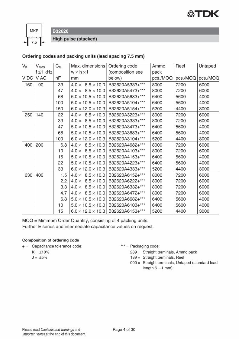
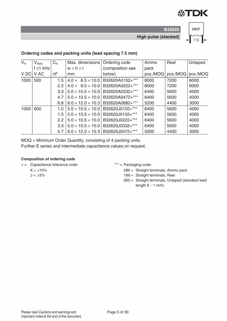
Ordering codes and packing units (lead spacing 7.5 mm)
VR
V DC
VRMSf ≤1 kHzV AC
CR
nF
Max. dimensionsw × h × lmm
Ordering code(composition seebelow)
Ammopackpcs./MOQ
Reel
pcs./MOQ
Untaped
pcs./MOQ
MOQ = Minimum Order Quantity, consisting of 4 packing units.Further E series and intermediate capacitance values on request.
Composition of ordering code+ = Capacitance tolerance code: *** = Packaging code:
K = ±10%J = ±5%
289 = Straight terminals, Ammo pack189 = Straight terminals, Reel000 = Straight terminals, Untaped (standard lead
length 6 1 mm)
160 90 33 4.0 × 8.5 × 10.0 B32620A5333+*** 8000 7200 600047 4.0 × 8.5 × 10.0 B32620A5473+*** 8000 7200 600068 5.0 × 10.5 × 10.0 B32620A5683+*** 6400 5600 4000100 5.0 × 10.5 × 10.0 B32620A5104+*** 6400 5600 4000150 6.0 × 12.0 × 10.3 B32620A5154+*** 5200 4400 3000
250 140 22 4.0 × 8.5 × 10.0 B32620A3223+*** 8000 7200 600033 4.0 × 8.5 × 10.0 B32620A3333+*** 8000 7200 600047 5.0 × 10.5 × 10.0 B32620A3473+*** 6400 5600 400068 5.0 × 10.5 × 10.0 B32620A3683+*** 6400 5600 4000100 6.0 × 12.0 × 10.3 B32620A3104+*** 5200 4400 3000
400 200 6.8 4.0 × 8.5 × 10.0 B32620A4682+*** 8000 7200 600010 4.0 × 8.5 × 10.0 B32620A4103+*** 8000 7200 600015 5.0 × 10.5 × 10.0 B32620A4153+*** 6400 5600 400022 5.0 × 10.5 × 10.0 B32620A4223+*** 6400 5600 400033 6.0 × 12.0 × 10.3 B32620A4333+*** 5200 4400 3000
630 400 1.5 4.0 × 8.5 × 10.0 B32620A6152+*** 8000 7200 60002.2 4.0 × 8.5 × 10.0 B32620A6222+*** 8000 7200 60003.3 4.0 × 8.5 × 10.0 B32620A6332+*** 8000 7200 60004.7 4.0 × 8.5 × 10.0 B32620A6472+*** 8000 7200 60006.8 5.0 × 10.5 × 10.0 B32620A6682+*** 6400 5600 400010 5.0 × 10.5 × 10.0 B32620A6103+*** 6400 5600 400015 6.0 × 12.0 × 10.3 B32620A6153+*** 5200 4400 3000
B32620
High pulse (stacked)
Page 4 of 30Please read Cautions and warnings andImportant notes at the end of this document.
Ordering codes and packing units (lead spacing 7.5 mm)
VR
V DC
VRMSf ≤1 kHzV AC
CR
nF
Max. dimensionsw × h × lmm
Ordering code(composition seebelow)
Ammopackpcs./MOQ
Reel
pcs./MOQ
Untaped
pcs./MOQ
MOQ = Minimum Order Quantity, consisting of 4 packing units.Further E series and intermediate capacitance values on request.
Composition of ordering code+ = Capacitance tolerance code: *** = Packaging code:
K = ±10%J = ±5%
289 = Straight terminals, Ammo pack189 = Straight terminals, Reel000 = Straight terminals, Untaped (standard lead
length 6 1 mm)
1000 500 1.5 4.0 × 8.5 × 10.0 B32620A0152+*** 8000 7200 60002.2 4.0 × 8.5 × 10.0 B32620A0222+*** 8000 7200 60003.3 5.0 × 10.5 × 10.0 B32620A0332+*** 6400 5600 40004.7 5.0 × 10.5 × 10.0 B32620A0472+*** 6400 5600 40006.8 6.0 × 12.0 × 10.3 B32620A0682+*** 5200 4400 3000
1000 600 1.0 5.0 × 10.5 × 10.0 B32620J0102+*** 6400 5600 40001.5 5.0 × 10.5 × 10.0 B32620J0152+*** 6400 5600 40002.2 5.0 × 10.5 × 10.0 B32620J0222+*** 6400 5600 40003.3 5.0 × 10.5 × 10.0 B32620J0332+*** 6400 5600 40004.7 6.0 × 12.0 × 10.3 B32620J0472+*** 5200 4400 3000
B32620
High pulse (stacked)
Page 5 of 30Please read Cautions and warnings andImportant notes at the end of this document.
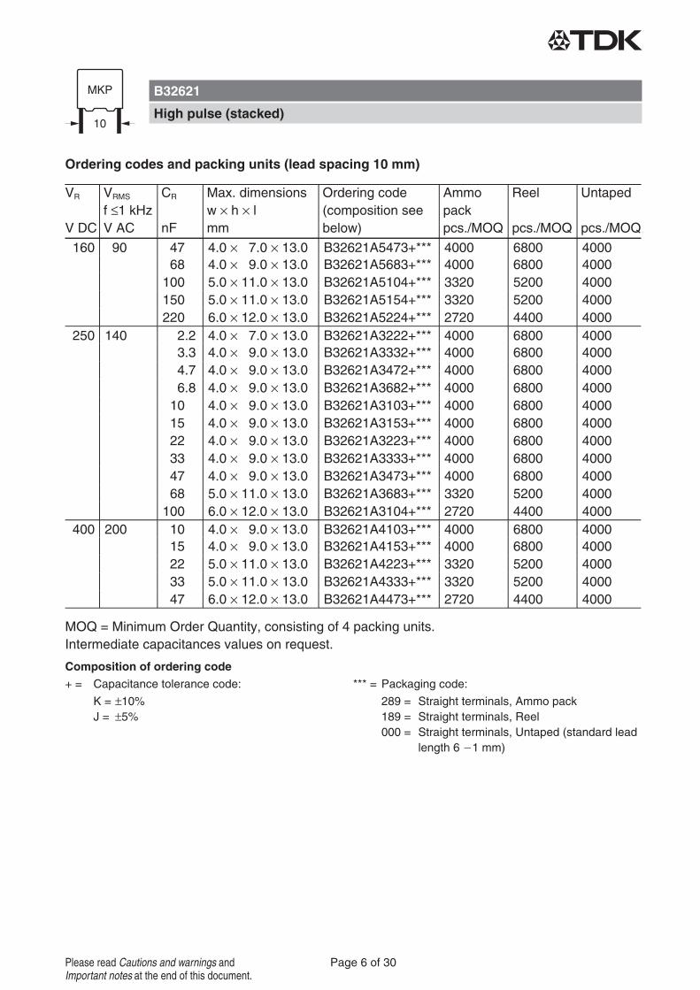
Ordering codes and packing units (lead spacing 10 mm)
VR
V DC
VRMSf ≤1 kHzV AC
CR
nF
Max. dimensionsw × h × lmm
Ordering code(composition seebelow)
Ammopackpcs./MOQ
Reel
pcs./MOQ
Untaped
pcs./MOQ
MOQ = Minimum Order Quantity, consisting of 4 packing units.Intermediate capacitances values on request.
Composition of ordering code+ = Capacitance tolerance code: *** = Packaging code:
K = ±10%J = ±5%
289 = Straight terminals, Ammo pack189 = Straight terminals, Reel000 = Straight terminals, Untaped (standard lead
length 6 1 mm)
160 90 47 4.0 × 7.0 × 13.0 B32621A5473+*** 4000 6800 400068 4.0 × 9.0 × 13.0 B32621A5683+*** 4000 6800 4000100 5.0 × 11.0 × 13.0 B32621A5104+*** 3320 5200 4000150 5.0 × 11.0 × 13.0 B32621A5154+*** 3320 5200 4000220 6.0 × 12.0 × 13.0 B32621A5224+*** 2720 4400 4000
250 140 2.2 4.0 × 7.0 × 13.0 B32621A3222+*** 4000 6800 40003.3 4.0 × 9.0 × 13.0 B32621A3332+*** 4000 6800 40004.7 4.0 × 9.0 × 13.0 B32621A3472+*** 4000 6800 40006.8 4.0 × 9.0 × 13.0 B32621A3682+*** 4000 6800 400010 4.0 × 9.0 × 13.0 B32621A3103+*** 4000 6800 400015 4.0 × 9.0 × 13.0 B32621A3153+*** 4000 6800 400022 4.0 × 9.0 × 13.0 B32621A3223+*** 4000 6800 400033 4.0 × 9.0 × 13.0 B32621A3333+*** 4000 6800 400047 4.0 × 9.0 × 13.0 B32621A3473+*** 4000 6800 400068 5.0 × 11.0 × 13.0 B32621A3683+*** 3320 5200 4000100 6.0 × 12.0 × 13.0 B32621A3104+*** 2720 4400 4000
400 200 10 4.0 × 9.0 × 13.0 B32621A4103+*** 4000 6800 400015 4.0 × 9.0 × 13.0 B32621A4153+*** 4000 6800 400022 5.0 × 11.0 × 13.0 B32621A4223+*** 3320 5200 400033 5.0 × 11.0 × 13.0 B32621A4333+*** 3320 5200 400047 6.0 × 12.0 × 13.0 B32621A4473+*** 2720 4400 4000
B32621
High pulse (stacked)
Page 6 of 30Please read Cautions and warnings andImportant notes at the end of this document.
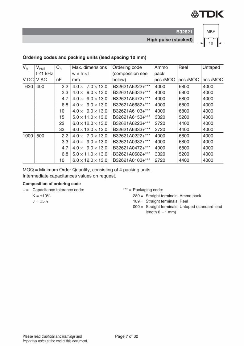
Ordering codes and packing units (lead spacing 10 mm)
VR
V DC
VRMSf ≤1 kHzV AC
CR
nF
Max. dimensionsw × h × lmm
Ordering code(composition seebelow)
Ammopackpcs./MOQ
Reel
pcs./MOQ
Untaped
pcs./MOQ
MOQ = Minimum Order Quantity, consisting of 4 packing units.Intermediate capacitances values on request.
Composition of ordering code+ = Capacitance tolerance code: *** = Packaging code:
K = ±10%J = ±5%
289 = Straight terminals, Ammo pack189 = Straight terminals, Reel000 = Straight terminals, Untaped (standard lead
length 6 1 mm)
630 400 2.2 4.0 × 7.0 × 13.0 B32621A6222+*** 4000 6800 40003.3 4.0 × 9.0 × 13.0 B32621A6332+*** 4000 6800 40004.7 4.0 × 9.0 × 13.0 B32621A6472+*** 4000 6800 40006.8 4.0 × 9.0 × 13.0 B32621A6682+*** 4000 6800 400010 4.0 × 9.0 × 13.0 B32621A6103+*** 4000 6800 400015 5.0 × 11.0 × 13.0 B32621A6153+*** 3320 5200 400022 6.0 × 12.0 × 13.0 B32621A6223+*** 2720 4400 400033 6.0 × 12.0 × 13.0 B32621A6333+*** 2720 4400 4000
1000 500 2.2 4.0 × 7.0 × 13.0 B32621A0222+*** 4000 6800 40003.3 4.0 × 9.0 × 13.0 B32621A0332+*** 4000 6800 40004.7 4.0 × 9.0 × 13.0 B32621A0472+*** 4000 6800 40006.8 5.0 × 11.0 × 13.0 B32621A0682+*** 3320 5200 400010 6.0 × 12.0 × 13.0 B32621A0103+*** 2720 4400 4000
B32621
High pulse (stacked)
Page 7 of 30Please read Cautions and warnings andImportant notes at the end of this document.
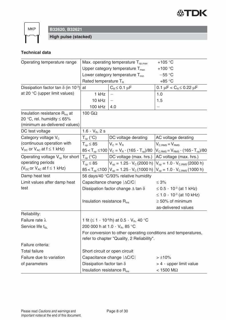
Technical data
Operating temperature range Max. operating temperature Top,max +105 °CUpper category temperature Tmax +100 °CLower category temperature Tmin 55 °CRated temperature TR +85 °C
Dissipation factor tan δ (in 10-3)at 20 °C (upper limit values)
at CR ≤ 0.1 μF 0.1 μF < CR ≤ 0.22 μF1 kHz 1.0
10 kHz 1.5
100 kHz 4.0
Insulation resistance Rins at20 °C, rel. humidity ≤ 65%(minimum as-delivered values)
100 GΩ
DC test voltage 1.6 VR, 2 s
Category voltage VC(continuous operation withVDC or VAC at f ≤ 1 kHz)
Top (°C) DC voltage derating AC voltage derating
Top ≤ 85 VC = VR VC,RMS =VRMS85<Top ≤100 VC = VR (165 - Top)/80 VC,RMS =VRMS (165 - Top)/80
Operating voltage Vop for shortoperating periods(VDC or VAC at f ≤ 1 kHz)
Top (°C) DC voltage (max. hrs.) AC voltage (max. hrs.)
Top ≤ 85 Vop = 1.25 VC (2000 h) Vop = 1.0 VC,RMS (2000 h)
85 <Top ≤100 Vop = 1.25 VC (1000 h) Vop = 1.0 VC,RMS (1000 h)
Damp heat test 56 days/40 °C/93% relative humidity
Limit values after damp heattest
Capacitance change ΔC/C ≤ 3%Dissipation factor change Δ tan δ ≤ 0.5 10-3 (at 1 kHz)
≤ 1.0 10-3 (at 10 kHz)
Insulation resistance Rins ≥ 50% of minimum
as-delivered values
Reliability:
Failure rate λ 1 fit (≤ 1 10-9/h) at 0.5 VR, 40 °CService life tSL 200 000 h at 1.0 VR, 85 °C
For conversion to other operating conditions and temperatures,refer to chapter "Quality, 2 Reliability".
Failure criteria:
Total failure Short circuit or open circuit
Failure due to variation Capacitance change ΔC/C > ±10%of parameters Dissipation factor tan δ > 4 upper limit value
Insulation resistance Rins < 1500 MΩ
B32620, B32621
High pulse (stacked)
Page 8 of 30Please read Cautions and warnings andImportant notes at the end of this document.
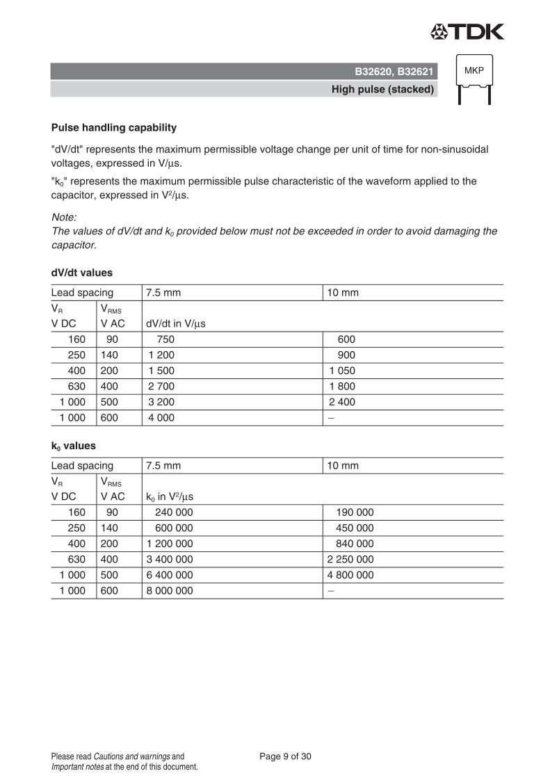
Pulse handling capability
"dV/dt" represents the maximum permissible voltage change per unit of time for non-sinusoidalvoltages, expressed in V/μs.
"k0" represents the maximum permissible pulse characteristic of the waveform applied to thecapacitor, expressed in V2/μs.
Note:The values of dV/dt and k0 provided below must not be exceeded in order to avoid damaging thecapacitor.
dV/dt values
Lead spacing 7.5 mm 10 mm
VR VRMSV DC V AC dV/dt in V/μs
160 90 750 600
250 140 1 200 900
400 200 1 500 1 050
630 400 2 700 1 800
1 000 500 3 200 2 400
1 000 600 4 000
k0 values
Lead spacing 7.5 mm 10 mm
VR VRMSV DC V AC k0 in V2/μs
160 90 240 000 190 000
250 140 600 000 450 000
400 200 1 200 000 840 000
630 400 3 400 000 2 250 000
1 000 500 6 400 000 4 800 000
1 000 600 8 000 000
B32620, B32621
High pulse (stacked)
Page 9 of 30Please read Cautions and warnings andImportant notes at the end of this document.
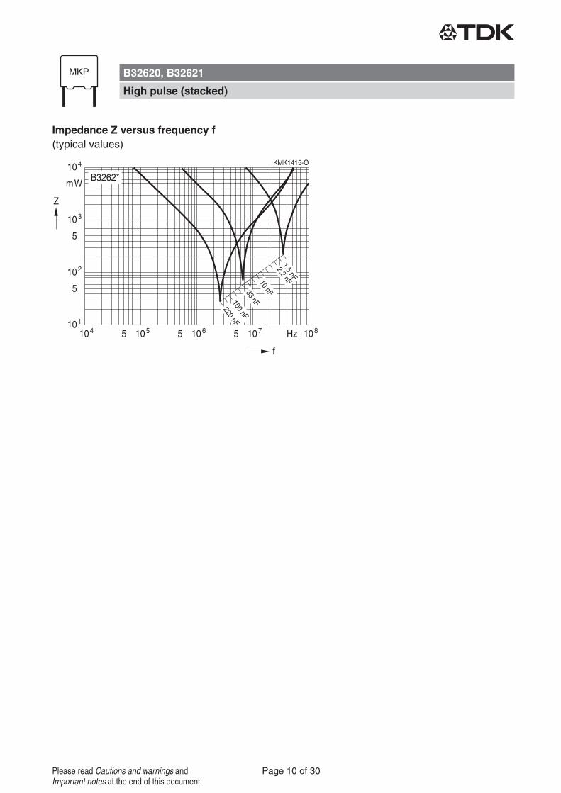
Impedance Z versus frequency f(typical values)
B32620, B32621
High pulse (stacked)
Page 10 of 30Please read Cautions and warnings andImportant notes at the end of this document.
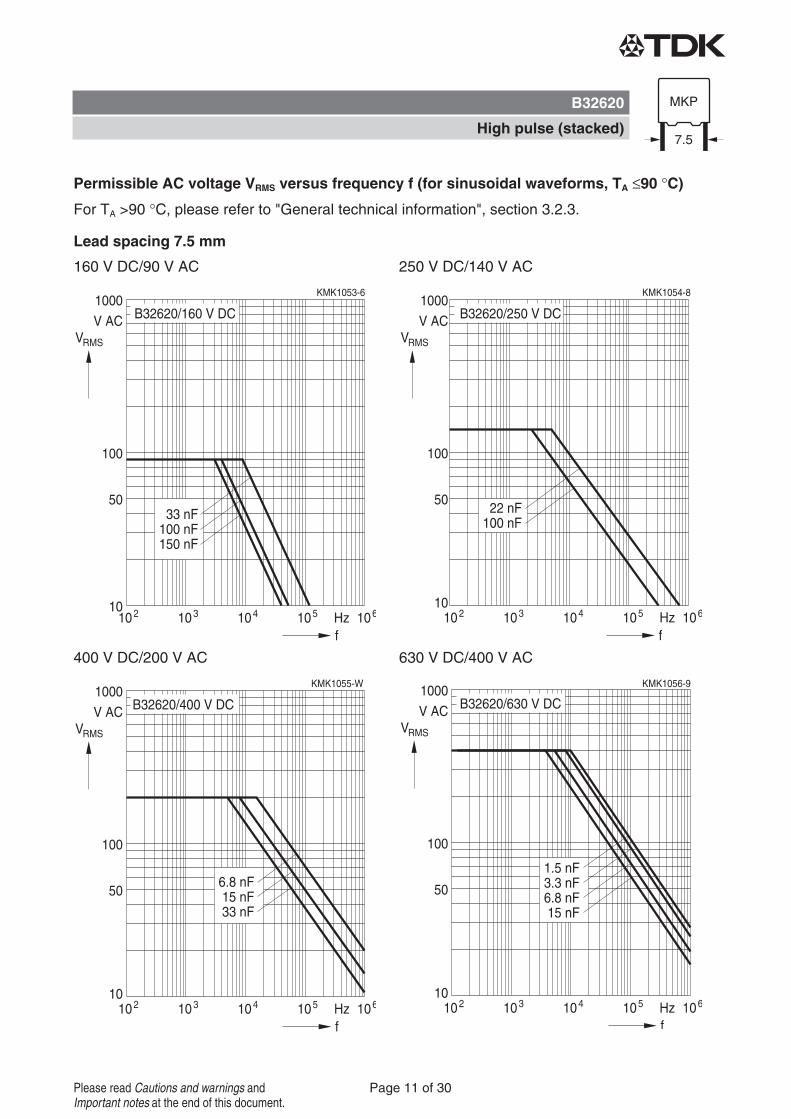
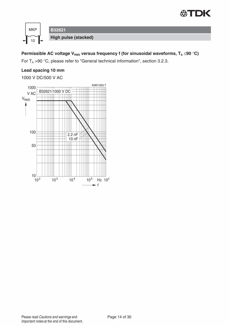
Permissible AC voltage VRMS versus frequency f (for sinusoidal waveforms, TA ≤90 °C)
For TA >90 °C, please refer to "General technical information", section 3.2.3.
Lead spacing 7.5 mm
160 V DC/90 V AC 250 V DC/140 V AC
400 V DC/200 V AC 630 V DC/400 V AC
B32620
High pulse (stacked)
Page 11 of 30Please read Cautions and warnings andImportant notes at the end of this document.
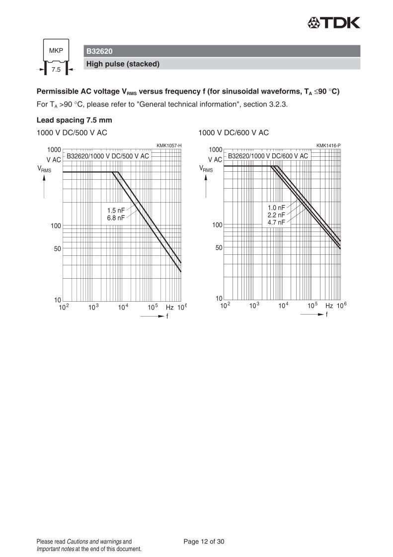
Permissible AC voltage VRMS versus frequency f (for sinusoidal waveforms, TA ≤90 °C)
For TA >90 °C, please refer to "General technical information", section 3.2.3.
Lead spacing 7.5 mm
1000 V DC/500 V AC 1000 V DC/600 V AC
B32620
High pulse (stacked)
Page 12 of 30Please read Cautions and warnings andImportant notes at the end of this document.
Permissible AC voltage VRMS versus frequency f (for sinusoidal waveforms, TA ≤90 °C)
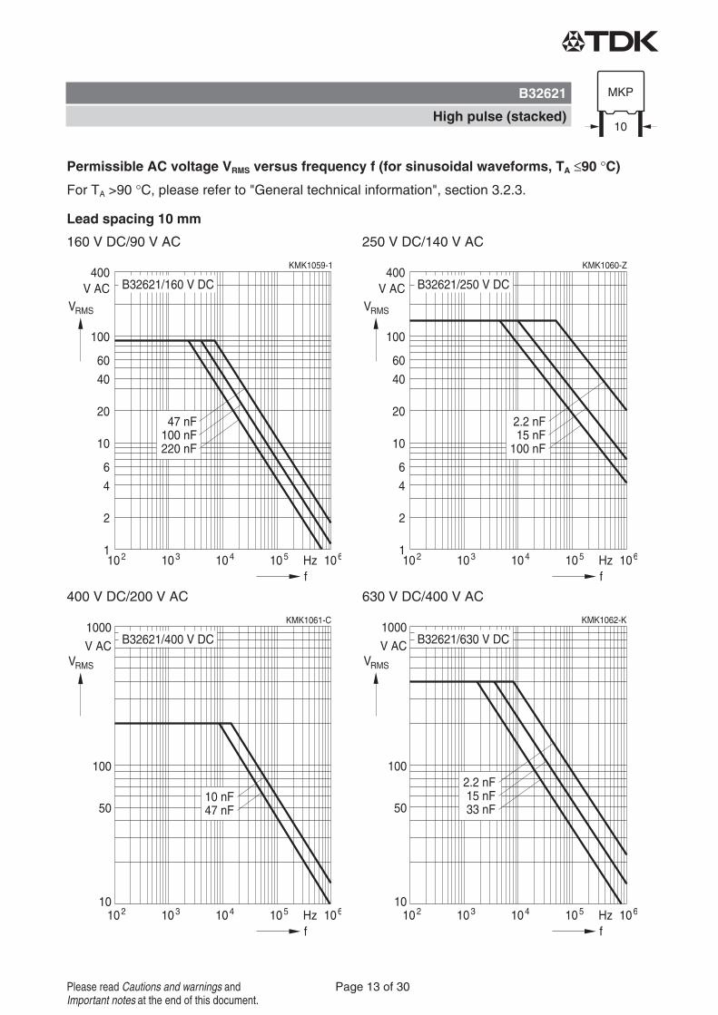
For TA >90 °C, please refer to "General technical information", section 3.2.3.
Lead spacing 10 mm
160 V DC/90 V AC 250 V DC/140 V AC
400 V DC/200 V AC 630 V DC/400 V AC
B32621
High pulse (stacked)
Page 13 of 30Please read Cautions and warnings andImportant notes at the end of this document.
Permissible AC voltage VRMS versus frequency f (for sinusoidal waveforms, TA ≤90 °C)
For TA >90 °C, please refer to "General technical information", section 3.2.3.
Lead spacing 10 mm
1000 V DC/500 V AC
B32621
High pulse (stacked)
Page 14 of 30Please read Cautions and warnings andImportant notes at the end of this document.
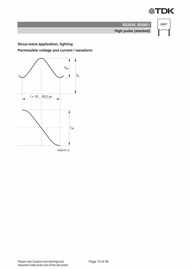
Sinus-wave application, lighting
Permissible voltage and current / waveform
B32620, B32621
High pulse (stacked)
Page 15 of 30Please read Cautions and warnings andImportant notes at the end of this document.
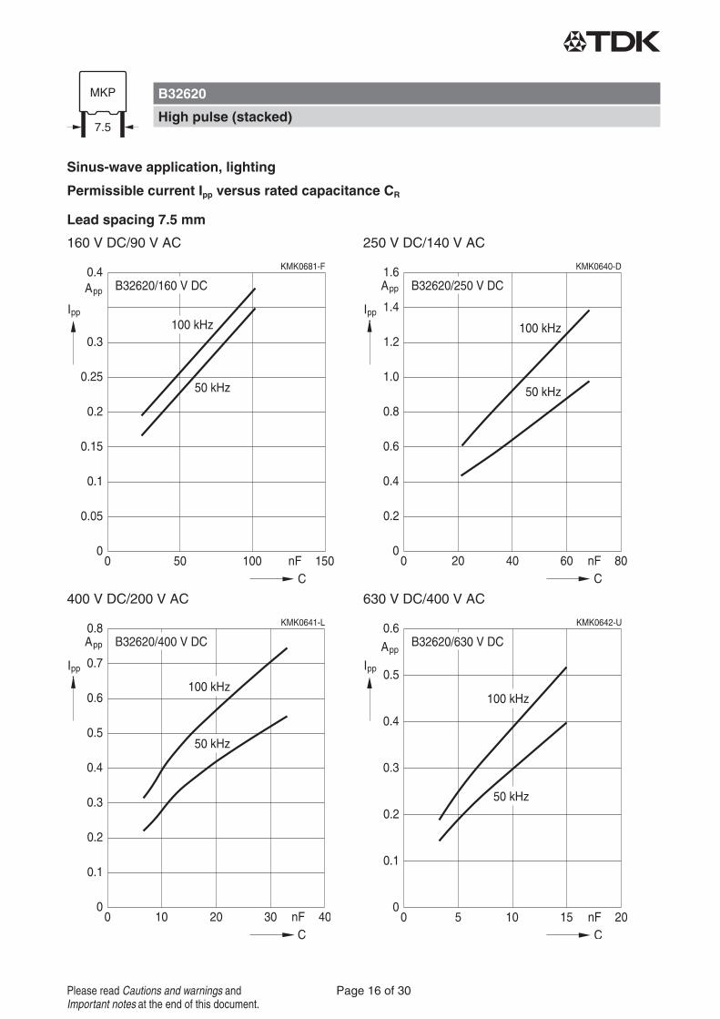
Sinus-wave application, lighting
Permissible current Ipp versus rated capacitance CR
Lead spacing 7.5 mm
160 V DC/90 V AC 250 V DC/140 V AC
400 V DC/200 V AC 630 V DC/400 V AC
B32620
High pulse (stacked)
Page 16 of 30Please read Cautions and warnings andImportant notes at the end of this document.
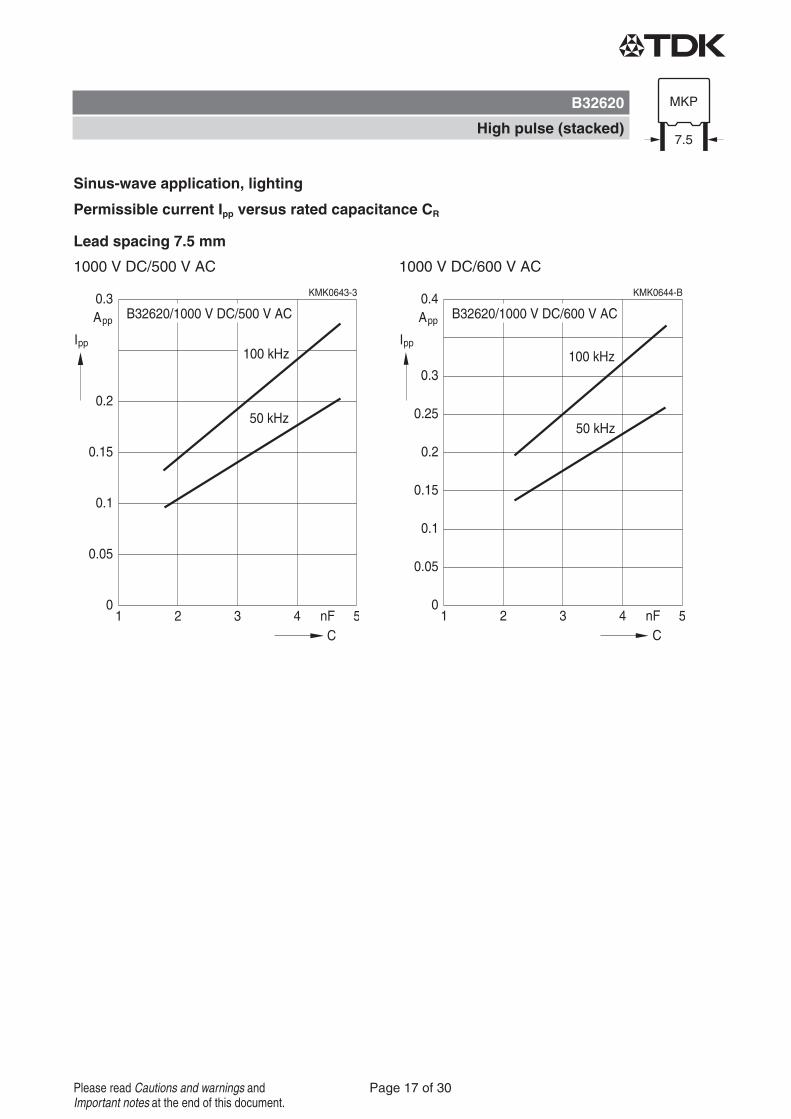
Sinus-wave application, lighting
Permissible current Ipp versus rated capacitance CR
Lead spacing 7.5 mm
1000 V DC/500 V AC 1000 V DC/600 V AC
B32620
High pulse (stacked)
Page 17 of 30Please read Cautions and warnings andImportant notes at the end of this document.
Sinus-wave application, lighting
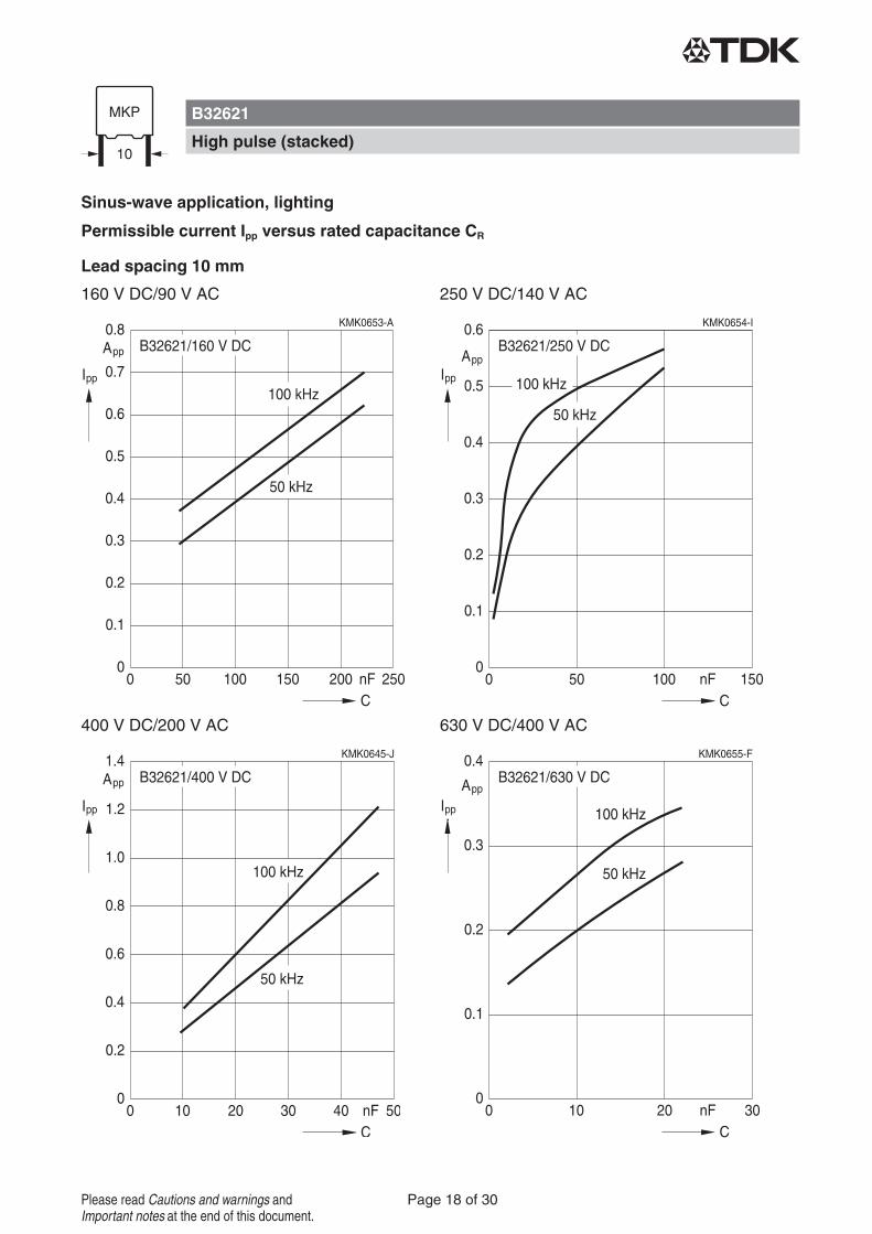
Permissible current Ipp versus rated capacitance CR
Lead spacing 10 mm
160 V DC/90 V AC 250 V DC/140 V AC
400 V DC/200 V AC 630 V DC/400 V AC
B32621
High pulse (stacked)
Page 18 of 30Please read Cautions and warnings andImportant notes at the end of this document.
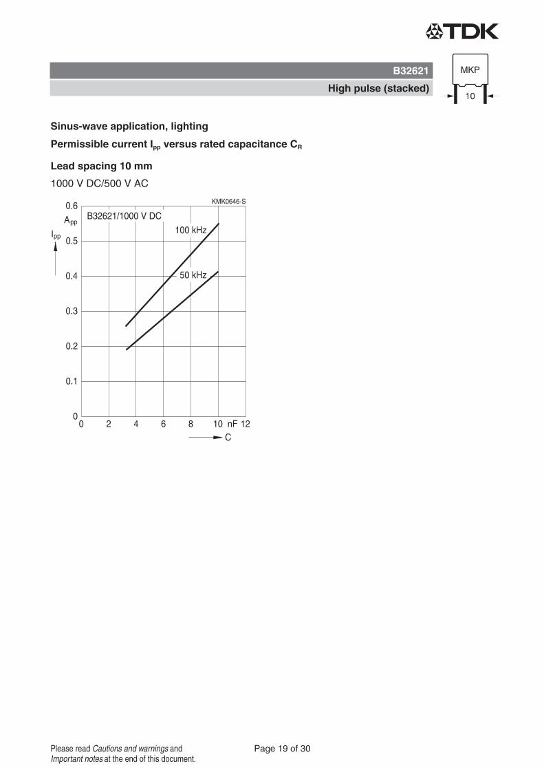
Sinus-wave application, lighting
Permissible current Ipp versus rated capacitance CR
Lead spacing 10 mm
1000 V DC/500 V AC
B32621
High pulse (stacked)
Page 19 of 30Please read Cautions and warnings andImportant notes at the end of this document.

Mounting guidelines
1 Soldering
1.1 Solderability of leads
The solderability of terminal leads is tested to IEC 60068-2-20:2008, test Ta, method 1.
Before a solderability test is carried out, terminals are subjected to accelerated ageing (toIEC 60068-2-2:2007, test Ba: 4 h exposure to dry heat at 155 °C). Since the ageing temperatureis far higher than the upper category temperature of the capacitors, the terminal wires should becut off from the capacitor before the ageing procedure to prevent the solderability being impairedby the products of any capacitor decomposition that might occur.
Solder bath temperature 235 ±5 °CSoldering time 2.0 ±0.5 sImmersion depth 2.0 +0/ 0.5 mm from capacitor body or seating plane
Evaluation criteria:
Visual inspectionWetting of wire surface by new solder ≥90%,free-flowing solder
1.2 Resistance to soldering heat
Resistance to soldering heat is tested to IEC 60068-2-20:2008, test Tb, method 1.Conditions:
Series Solder bath temperature Soldering time
MKT boxed (except 2.5 × 6.5 × 7.2 mm)coateduncoated (lead spacing >10 mm)
260 ±5 °C 10 ±1 s
MFPMKP (lead spacing >7.5 mm)
MKT boxed (case 2.5 × 6.5 × 7.2 mm) 5 ±1 sMKPMKT
(lead spacing ≤7.5 mm)uncoated (lead spacing ≤10 mm)insulated (B32559)
<4 srecommended solderingprofile for MKT uncoated(lead spacing ≤ 10 mm) andinsulated (B32559)
B32620, B32621
High pulse (stacked)
Page 20 of 30Please read Cautions and warnings andImportant notes at the end of this document.

Immersion depth 2.0 +0/ 0.5 mm from capacitor body or seating plane
Shield Heat-absorbing board, (1.5 ±0.5) mm thick, betweencapacitor body and liquid solder
Evaluation criteria:
Visual inspection No visible damage
ΔC/C02% for MKT/MKP/MFP5% for EMI suppression capacitors
tan δ As specified in sectional specification
1.3 General notes on soldering
Permissible heat exposure loads on film capacitors are primarily characterized by the upper cate-gory temperature Tmax. Long exposure to temperatures above this type-related temperature limitcan lead to changes in the plastic dielectric and thus change irreversibly a capacitor's electricalcharacteristics. For short exposures (as in practical soldering processes) the heat load (and thusthe possible effects on a capacitor) will also depend on other factors like:
Pre-heating temperature and timeForced cooling immediately after solderingTerminal characteristics:diameter, length, thermal resistance, special configurations (e.g. crimping)Height of capacitor above solder bathShadowing by neighboring componentsAdditional heating due to heat dissipation by neighboring componentsUse of solder-resist coatings
B32620, B32621
High pulse (stacked)
Page 21 of 30Please read Cautions and warnings andImportant notes at the end of this document.
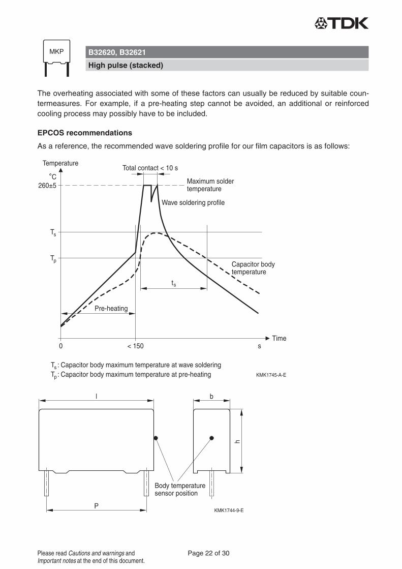
The overheating associated with some of these factors can usually be reduced by suitable coun-termeasures. For example, if a pre-heating step cannot be avoided, an additional or reinforcedcooling process may possibly have to be included.
EPCOS recommendations
As a reference, the recommended wave soldering profile for our film capacitors is as follows:
B32620, B32621
High pulse (stacked)
Page 22 of 30Please read Cautions and warnings andImportant notes at the end of this document.
Body temperature should follow the description below:
MKP capacitorDuring pre-heating: Tp ≤110 °CDuring soldering: Ts ≤120 °C, ts ≤45 s
MKT capacitorDuring pre-heating: Tp ≤125 °CDuring soldering: Ts ≤160 °C, ts ≤45 s
When SMD components are used together with leaded ones, the film capacitors should not passinto the SMD adhesive curing oven. The leaded components should be assembled after the SMDcuring step.
Leaded film capacitors are not suitable for reflow soldering.
In order to ensure proper conditions for manual or selective soldering, the body temperature ofthe capacitor (Ts) must be ≤120 °C.
One recommended condition for manual soldering is that the tip of the soldering iron shouldbe <360 °C and the soldering contact time should be no longer than 3 seconds.
For uncoated MKT capacitors with lead spacings ≤10 mm (B32560/B32561) the following mea-sures are recommended:
pre-heating to not more than 110 °C in the preheater phaserapid cooling after soldering
Please refer to EPCOS Film Capacitor Data Book in case more details are needed.
B32620, B32621
High pulse (stacked)
Page 23 of 30Please read Cautions and warnings andImportant notes at the end of this document.
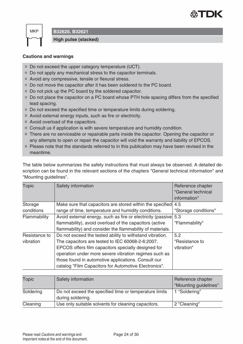
Cautions and warnings
Do not exceed the upper category temperature (UCT).Do not apply any mechanical stress to the capacitor terminals.Avoid any compressive, tensile or flexural stress.Do not move the capacitor after it has been soldered to the PC board.Do not pick up the PC board by the soldered capacitor.Do not place the capacitor on a PC board whose PTH hole spacing differs from the specifiedlead spacing.Do not exceed the specified time or temperature limits during soldering.Avoid external energy inputs, such as fire or electricity.Avoid overload of the capacitors.Consult us if application is with severe temperature and humidity condition.There are no serviceable or repairable parts inside the capacitor. Opening the capacitor orany attempts to open or repair the capacitor will void the warranty and liability of EPCOS.Please note that the standards referred to in this publication may have been revised in themeantime.
The table below summarizes the safety instructions that must always be observed. A detailed de-scription can be found in the relevant sections of the chapters "General technical information" and"Mounting guidelines".
Topic Safety information Reference chapter"General technicalinformation"
Storageconditions
Make sure that capacitors are stored within the specifiedrange of time, temperature and humidity conditions.
4.5"Storage conditions"
Flammability Avoid external energy, such as fire or electricity (passiveflammability), avoid overload of the capacitors (activeflammability) and consider the flammability of materials.
5.3"Flammability"
Resistance tovibration
Do not exceed the tested ability to withstand vibration.The capacitors are tested to IEC 60068-2-6:2007.EPCOS offers film capacitors specially designed foroperation under more severe vibration regimes such asthose found in automotive applications. Consult ourcatalog "Film Capacitors for Automotive Electronics".
5.2"Resistance tovibration"
Topic Safety information Reference chapter"Mounting guidelines"
Soldering Do not exceed the specified time or temperature limitsduring soldering.
1 "Soldering"
Cleaning Use only suitable solvents for cleaning capacitors. 2 "Cleaning"
B32620, B32621
High pulse (stacked)
Page 24 of 30Please read Cautions and warnings andImportant notes at the end of this document.

Topic Safety information Reference chapter"Mounting guidelines"
Embedding ofcapacitors infinishedassemblies
When embedding finished circuit assemblies in plasticresins, chemical and thermal influences must be takeninto account.Caution: Consult us first, if you also wish to embed otheruncoated component types!
3 "Embedding ofcapacitors in finishedassemblies"
Display of ordering codes for EPCOS products
The ordering code for one and the same product can be represented differently in data sheets,data books, other publications and the website of EPCOS, or in order-related documents such asshipping notes, order confirmations and product labels. The varying representations of the or-dering codes are due to different processes employed and do not affect the specificationsof the respective products. Detailed information can be found on the Internet underwww.epcos.com/orderingcodes.
B32620, B32621
High pulse (stacked)
Page 25 of 30Please read Cautions and warnings andImportant notes at the end of this document.
Symbols and terms
Symbol English German
α Heat transfer coefficient Wärmeübergangszahl
αC Temperature coefficient of capacitance Temperaturkoeffizient der Kapazität
A Capacitor surface area Kondensatoroberfläche
βC Humidity coefficient of capacitance Feuchtekoeffizient der Kapazität
C Capacitance Kapazität
CR Rated capacitance Nennkapazität
ΔC Absolute capacitance change Absolute Kapazitätsänderung
ΔC/C Relative capacitance change (relativedeviation of actual value)
Relative Kapazitätsänderung (relativeAbweichung vom Ist-Wert)
ΔC/CR Capacitance tolerance (relative deviationfrom rated capacitance)
Kapazitätstoleranz (relative Abweichungvom Nennwert)
dt Time differential Differentielle Zeit
Δt Time interval Zeitintervall
ΔT Absolute temperature change(self-heating)
Absolute Temperaturänderung(Selbsterwärmung)
Δtan δ Absolute change of dissipation factor Absolute Änderung des Verlustfaktors
ΔV Absolute voltage change Absolute Spannungsänderung
dV/dt Time differential of voltage function (rateof voltage rise)
Differentielle Spannungsänderung(Spannungsflankensteilheit)
ΔV/Δt Voltage change per time interval Spannungsänderung pro Zeitintervall
E Activation energy for diffusion Aktivierungsenergie zur Diffusion
ESL Self-inductance Eigeninduktivität
ESR Equivalent series resistance Ersatz-Serienwiderstand
f Frequency Frequenz
f1 Frequency limit for reducing permissibleAC voltage due to thermal limits
Grenzfrequenz für thermisch bedingteReduzierung der zulässigenWechselspannung
f2 Frequency limit for reducing permissibleAC voltage due to current limit
Grenzfrequenz für strombedingteReduzierung der zulässigenWechselspannung
fr Resonant frequency Resonanzfrequenz
FD Thermal acceleration factor for diffusion Therm. Beschleunigungsfaktor zurDiffusion
FT Derating factor Deratingfaktor
i Current (peak) Stromspitze
IC Category current (max. continuouscurrent)
Kategoriestrom (max. Dauerstrom)
B32620, B32621
High pulse (stacked)
Page 26 of 30Please read Cautions and warnings andImportant notes at the end of this document.
Symbol English German
IRMS (Sinusoidal) alternating current,root-mean-square value
(Sinusförmiger) Wechselstrom
iz Capacitance drift Inkonstanz der Kapazität
k0 Pulse characteristic Impulskennwert
LS Series inductance Serieninduktivität
λ Failure rate Ausfallrate
λ0 Constant failure rate during usefulservice life
Konstante Ausfallrate in derNutzungsphase
λtest Failure rate, determined by tests Experimentell ermittelte Ausfallrate
Pdiss Dissipated power Abgegebene Verlustleistung
Pgen Generated power Erzeugte Verlustleistung
Q Heat energy Wärmeenergie
ρ Density of water vapor in air Dichte von Wasserdampf in Luft
R Universal molar constant for gases Allg. Molarkonstante für Gas
R Ohmic resistance of discharge circuit Ohmscher Widerstand desEntladekreises
Ri Internal resistance Innenwiderstand
Rins Insulation resistance Isolationswiderstand
RP Parallel resistance Parallelwiderstand
RS Series resistance Serienwiderstand
S severity (humidity test) Schärfegrad (Feuchtetest)
t Time Zeit
T Temperature Temperatur
τ Time constant Zeitkonstante
tan δ Dissipation factor Verlustfaktor
tan δD Dielectric component of dissipationfactor
Dielektrischer Anteil des Verlustfaktors
tan δP Parallel component of dissipation factor Parallelanteil des Verlfustfaktors
tan δS Series component of dissipation factor Serienanteil des Verlustfaktors
TA Temperature of the air surrounding thecomponent
Temperatur der Luft, die das Bauteilumgibt
Tmax Upper category temperature Obere Kategorietemperatur
Tmin Lower category temperature Untere Kategorietemperatur
tOL Operating life at operating temperatureand voltage
Betriebszeit bei Betriebstemperatur und-spannung
Top Operating temperature, TA + ΔT Beriebstemperatur, TA + ΔTTR Rated temperature Nenntemperatur
Tref Reference temperature Referenztemperatur
tSL Reference service life Referenz-Lebensdauer
B32620, B32621
High pulse (stacked)
Page 27 of 30Please read Cautions and warnings andImportant notes at the end of this document.
Symbol English German
VAC AC voltage Wechselspannung
VC Category voltage Kategoriespannung
VC,RMS Category AC voltage (Sinusförmige)Kategorie-Wechselspannung
VCD Corona-discharge onset voltage Teilentlade-Einsatzspannung
Vch Charging voltage Ladespannung
VDC DC voltage Gleichspannung
VFB Fly-back capacitor voltage Spannung (Flyback)
Vi Input voltage Eingangsspannung
Vo Output voltage Ausgangssspannung
Vop Operating voltage Betriebsspannung
Vp Peak pulse voltage Impuls-Spitzenspannung
Vpp Peak-to-peak voltage Impedance Spannungshub
VR Rated voltage Nennspannung
R Amplitude of rated AC voltage Amplitude der Nenn-Wechselspannung
VRMS (Sinusoidal) alternating voltage,root-mean-square value
(Sinusförmige) Wechselspannung
VSC S-correction voltage Spannung bei Anwendung "S-correction"
Vsn Snubber capacitor voltage Spannung bei Anwendung"Beschaltung"
Z Impedance Scheinwiderstand
Lead spacing Rastermaß
B32620, B32621
High pulse (stacked)
Page 28 of 30Please read Cautions and warnings andImportant notes at the end of this document.
The following applies to all products named in this publication:1. Some parts of this publication contain statements about the suitability of our products for
certain areas of application. These statements are based on our knowledge of typical re-quirements that are often placed on our products in the areas of application concerned. Wenevertheless expressly point out that such statements cannot be regarded as bindingstatements about the suitability of our products for a particular customer application.As a rule, EPCOS is either unfamiliar with individual customer applications or less familiarwith them than the customers themselves. For these reasons, it is always ultimately incum-bent on the customer to check and decide whether an EPCOS product with the properties de-scribed in the product specification is suitable for use in a particular customer application.
2. We also point out that in individual cases, a malfunction of electronic components orfailure before the end of their usual service life cannot be completely ruled out in thecurrent state of the art, even if they are operated as specified. In customer applicationsrequiring a very high level of operational safety and especially in customer applications inwhich the malfunction or failure of an electronic component could endanger human life orhealth (e.g. in accident prevention or lifesaving systems), it must therefore be ensured bymeans of suitable design of the customer application or other action taken by the customer(e.g. installation of protective circuitry or redundancy) that no injury or damage is sustained bythird parties in the event of malfunction or failure of an electronic component.
3. The warnings, cautions and product-specific notes must be observed.4. In order to satisfy certain technical requirements, some of the products described in this
publication may contain substances subject to restrictions in certain jurisdictions (e.g.because they are classed as hazardous). Useful information on this will be found in our Ma-terial Data Sheets on the Internet (www.epcos.com/material). Should you have any more de-tailed questions, please contact our sales offices.
5. We constantly strive to improve our products. Consequently, the products described in thispublication may change from time to time. The same is true of the corresponding productspecifications. Please check therefore to what extent product descriptions and specificationscontained in this publication are still applicable before or when you place an order. We alsoreserve the right to discontinue production and delivery of products. Consequently, wecannot guarantee that all products named in this publication will always be available. Theaforementioned does not apply in the case of individual agreements deviating from the fore-going for customer-specific products.
6. Unless otherwise agreed in individual contracts, all orders are subject to the current ver-sion of the "General Terms of Delivery for Products and Services in the Electrical In-dustry" published by the German Electrical and Electronics Industry Association(ZVEI).
Important notes
Page 29 of 30

7. Our manufacturing sites serving the automotive business apply the IATF 16949standard. The IATF certifications confirm our compliance with requirements regarding thequality management system in the automotive industry. Referring to customer requirementsand customer specific requirements (“CSR”) TDK always has and will continue to have thepolicy of respecting individual agreements. Even if IATF 16949 may appear to support theacceptance of unilateral requirements, we hereby like to emphasize that only requirementsmutually agreed upon can and will be implemented in our Quality Management System.For clarification purposes we like to point out that obligations from IATF 16949 shall onlybecome legally binding if individually agreed upon.
8. The trade names EPCOS, CeraCharge, CeraDiode, CeraLink, CeraPad, CeraPlas, CSMP,CTVS, DeltaCap, DigiSiMic, ExoCore, FilterCap, FormFit, LeaXield, MiniBlue, MiniCell, MKD,MKK, MotorCap, PCC, PhaseCap, PhaseCube, PhaseMod, PhiCap, PowerHap, PQSine,PQvar, SIFERRIT, SIFI, SIKOREL, SilverCap, SIMDAD, SiMic, SIMID, SineFormer, SIOV,ThermoFuse, WindCap are trademarks registered or pending in Europe and in other coun-tries. Further information will be found on the Internet at www.epcos.com/trademarks.
Release 2018-06
Important notes
Page 30 of 30