Field effect transistor - WordPress.com ( Field Effect Transistor) 1. ... The two gate regions of...
64
Field effect transistor Field effect transistor Svbitec.wordpress.com Assit.Prof. Vishal Jethva
Transcript of Field effect transistor - WordPress.com ( Field Effect Transistor) 1. ... The two gate regions of...

Field effect transistor Field effect transistor
Svbitec.wordpress.com
Assit.Prof. Vishal Jethva
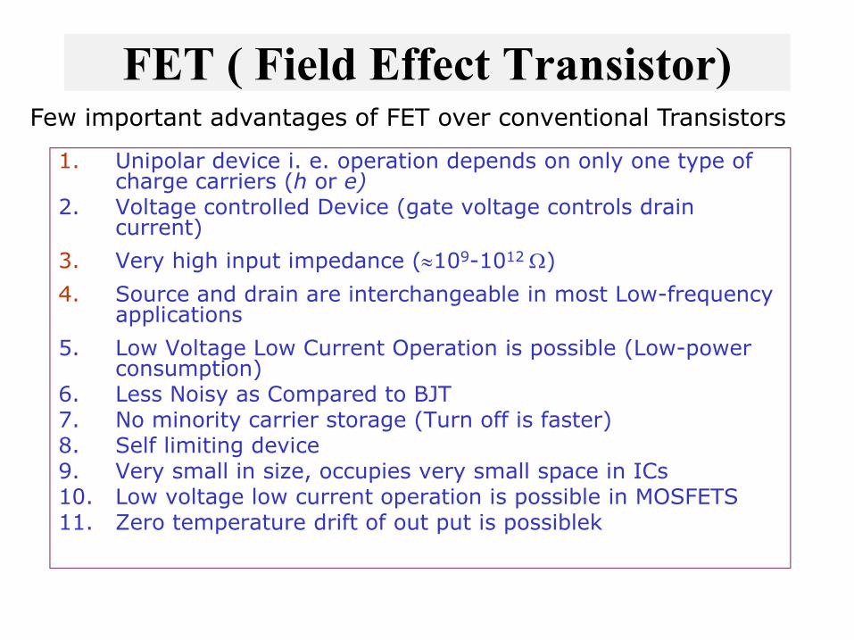
FET ( Field Effect Transistor)
1. Unipolar device i. e. operation depends on only one type of charge carriers (h or e)
2. Voltage controlled Device (gate voltage controls drain current)
3. Very high input impedance (109-1012 )
4. Source and drain are interchangeable in most Low-frequency applications
5. Low Voltage Low Current Operation is possible (Low-power consumption)
6. Less Noisy as Compared to BJT 7. No minority carrier storage (Turn off is faster) 8. Self limiting device 9. Very small in size, occupies very small space in ICs 10. Low voltage low current operation is possible in MOSFETS 11. Zero temperature drift of out put is possiblek
Few important advantages of FET over conventional Transistors
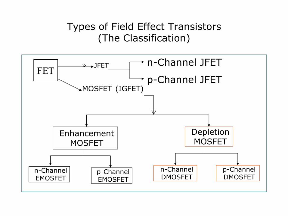
Types of Field Effect Transistors (The Classification)
» JFET
MOSFET (IGFET)
n-Channel JFET
p-Channel JFET
n-Channel EMOSFET
p-Channel EMOSFET
Enhancement MOSFET
Depletion MOSFET
n-Channel DMOSFET
p-Channel DMOSFET
FET
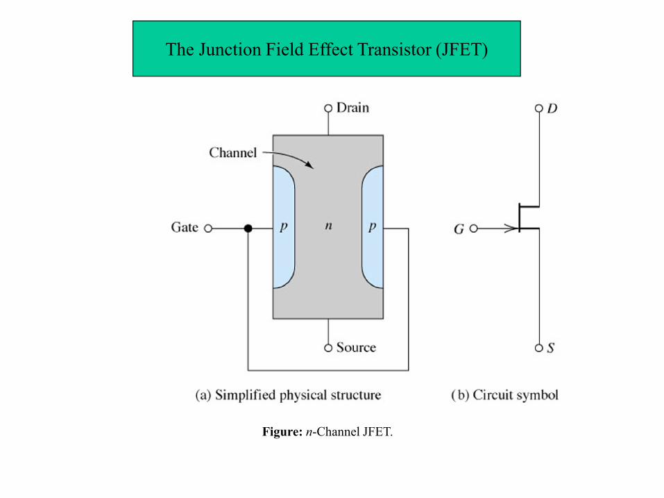
Figure: n-Channel JFET.
The Junction Field Effect Transistor (JFET)

Gate
Drain
Source
SYMBOLS
n-channel JFET
Gate
Drain
Source
n-channel JFET Offset-gate symbol
Gate
Drain
Source
p-channel JFET
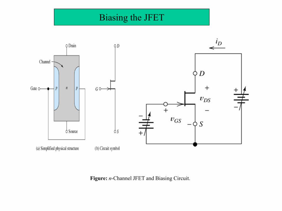
Figure: n-Channel JFET and Biasing Circuit.
Biasing the JFET
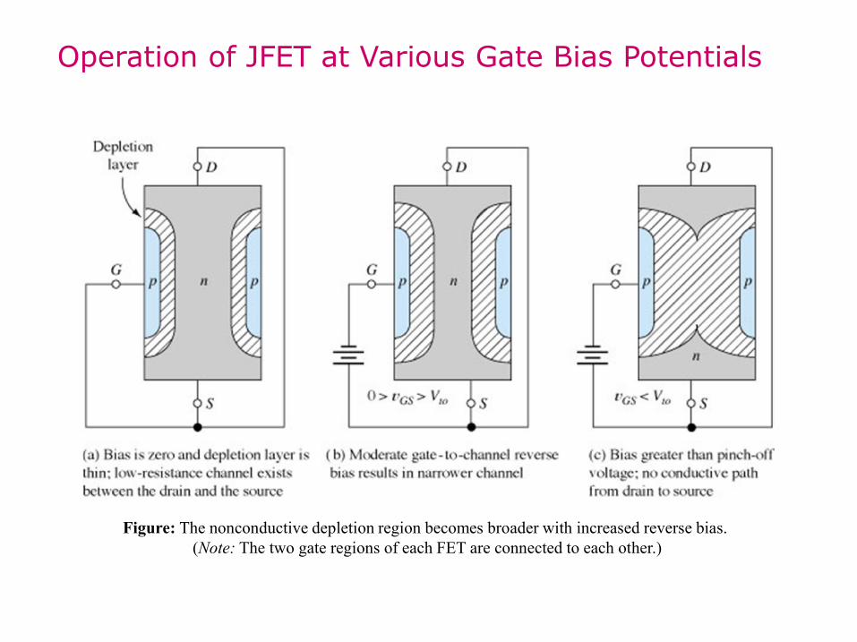
Figure: The nonconductive depletion region becomes broader with increased reverse bias. (Note: The two gate regions of each FET are connected to each other.)
Operation of JFET at Various Gate Bias Potentials
P P +
-
+
- +
-
N
N
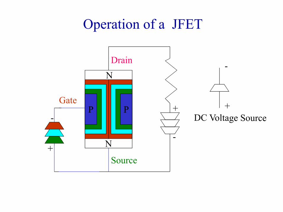
Operation of a JFET
Gate
Drain
Source
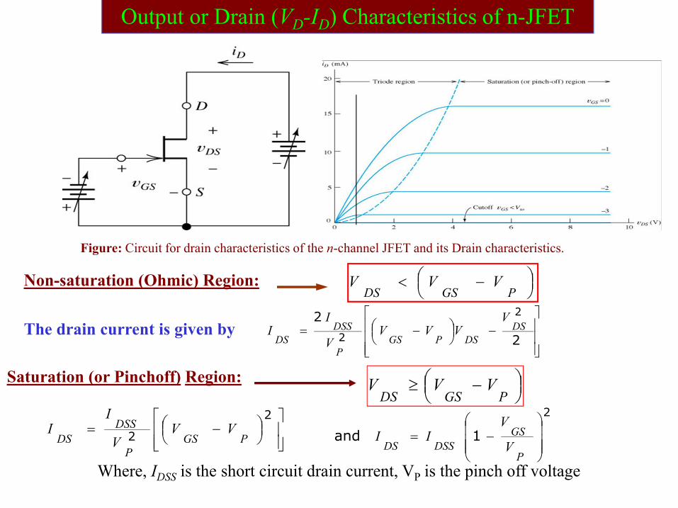
Figure: Circuit for drain characteristics of the n-channel JFET and its Drain characteristics.
Non-saturation (Ohmic) Region:
The drain current is given by
2
2 2
2DS
DSPGSP
DSS
DS
VVVV
V
II
2
2 PGSP
DSS
DSVV
V
II
2
1 and
P
GS
DSSDS V
VII
Where, IDSS is the short circuit drain current, VP is the pinch off voltage
Output or Drain (VD-ID) Characteristics of n-JFET
Saturation (or Pinchoff) Region:
PGSDSVVV
PGSDSVVV
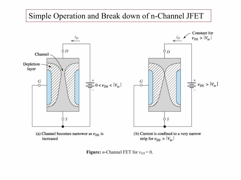
Figure: n-Channel FET for vGS = 0.
Simple Operation and Break down of n-Channel JFET
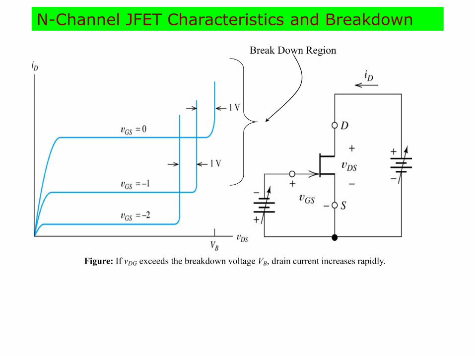
Figure: If vDG exceeds the breakdown voltage VB, drain current increases rapidly.
Break Down Region
N-Channel JFET Characteristics and Breakdown
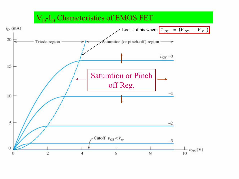
Figure: Typical drain characteristics of an n-channel JFET.
VD-ID Characteristics of EMOS FET
Saturation or Pinch off Reg.
Locus of pts where PGSDS VVV
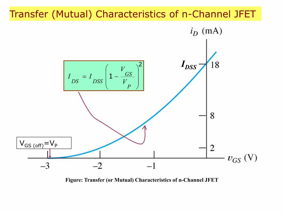
Figure: Transfer (or Mutual) Characteristics of n-Channel JFET
2
1
P
GS
DSSDS V
VII
IDSS
VGS (off)=VP
Transfer (Mutual) Characteristics of n-Channel JFET
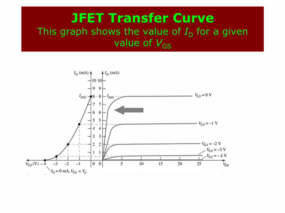
JFET Transfer Curve This graph shows the value of ID for a given
value of VGS

Biasing Circuits used for JFET
• Fixed bias circuit
• Self bias circuit
• Potential Divider bias circuit
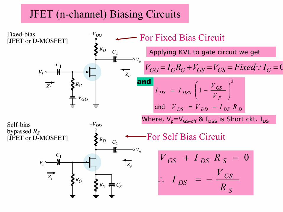
JFET (n-channel) Biasing Circuits
2
1
P
GS
DSSDS V
VII
0, GGSGSGGGG IFixedVVRIV
DDSDDDS
P
GSDSSDS
RIVV
V
VII
and
1
2
S
GSDS
SDSGS
R
VI
RIV
0
For Self Bias Circuit
For Fixed Bias Circuit
Applying KVL to gate circuit we get
and
Where, Vp=VGS-off & IDSS is Short ckt. IDS
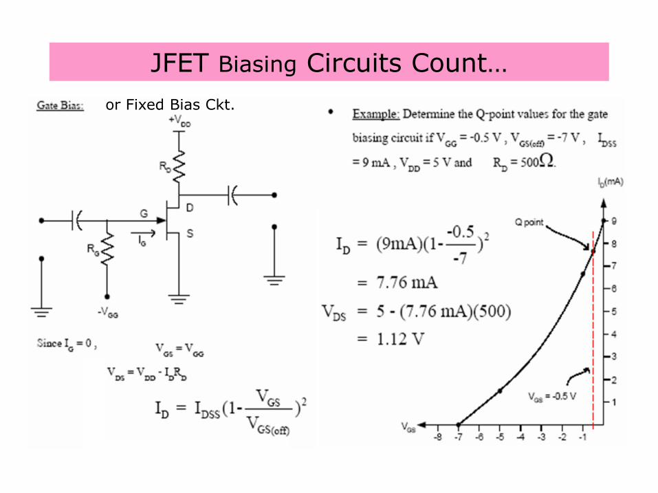
JFET Biasing Circuits Count…
or Fixed Bias Ckt.
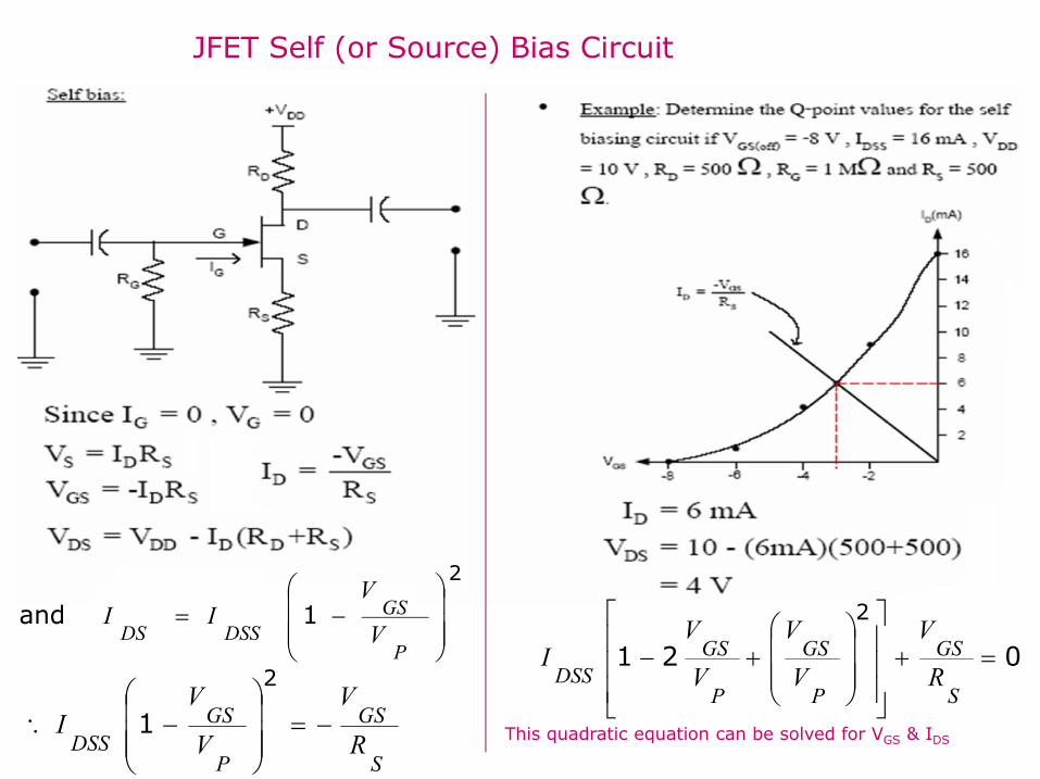
JFET Self (or Source) Bias Circuit
2
1 and
P
GS
DSSDS V
VII
S
GS
P
GS
DSS R
V
V
VI
2
1
021
2
S
GS
P
GS
P
GS
DSS R
V
V
V
V
VI
This quadratic equation can be solved for VGS & IDS
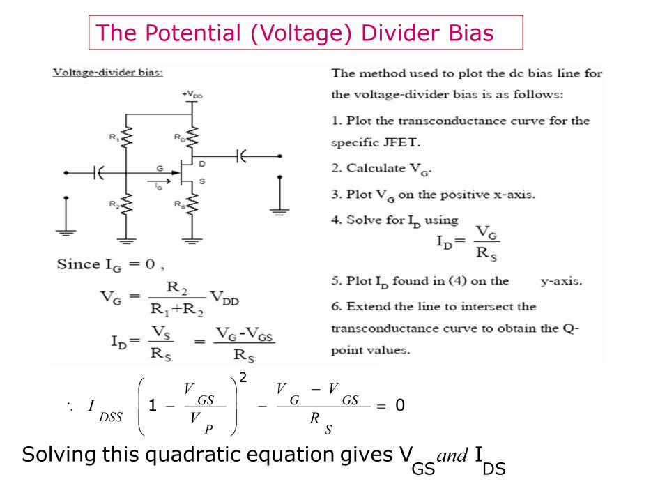
The Potential (Voltage) Divider Bias
01
2
S
GSG
P
GS
DSS R
VV
V
VI
DSGSI V gives equation quadratic this Solving and
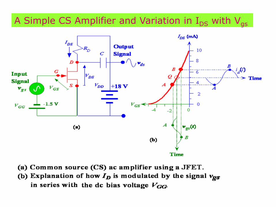
A Simple CS Amplifier and Variation in IDS with Vgs
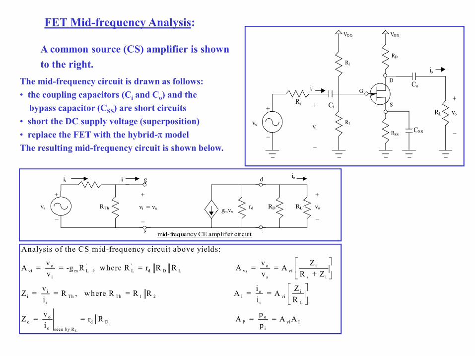
FET Mid-frequency Analysis:
g
s
rd gmvp vi = vp
ii io
vo
d
s
+ +
_ _
mid-frequency CE amplifier circuit
RD RL RTh vs
+
_
is
' 'o o ivi m L L d D L vs vi
i s s i
ii Th Th 1 2
i
Analysis of the CS mid-frequency circuit above yields:
v v ZA = = -g R , where R = r R R A = = A
v v R + Z
vZ = = R , where R = R R
i
L
o iI vi
i L
o oo d D P vi I
o iseen by R
i Z A = = A
i R
v pZ = = r R A = = A A
i p
A common source (CS) amplifier is shown
to the right.
Rs Ci
RL
Co
CSS vi
vo
+
+
vs
+
_ _
_
io
ii
D
S
G
VDD
VDD
R1
RSS
RD
R2
The mid-frequency circuit is drawn as follows:
• the coupling capacitors (Ci and Co) and the
bypass capacitor (CSS) are short circuits
• short the DC supply voltage (superposition)
• replace the FET with the hybrid-p model
The resulting mid-frequency circuit is shown below.

Procedure: Analysis of an FET amplifier at mid-frequency:
1) Find the DC Q-point. This will insure that the FET is operating in the saturation
region and these values are needed for the next step.
2) Find gm. If gm is not specified, calculate it using the DC values of VGS as follows:
3) Calculate the required values (typically Avi, Avs, AI, AP, Zi, and Zo. Use the formulas for
the appropriate amplifier configuration (CS, CG, CD, etc).
DSSDm GS P2
GS P
Dm GS T
GS
GS
2IIg = = V - V (for JFET's and DM MOSFET's)
V V
Ig = = V - V (for EM MOSFET's)
V
(Note: Uses DC value of V )
K
PE-Electrical Review Course - Class 4 (Transistors)
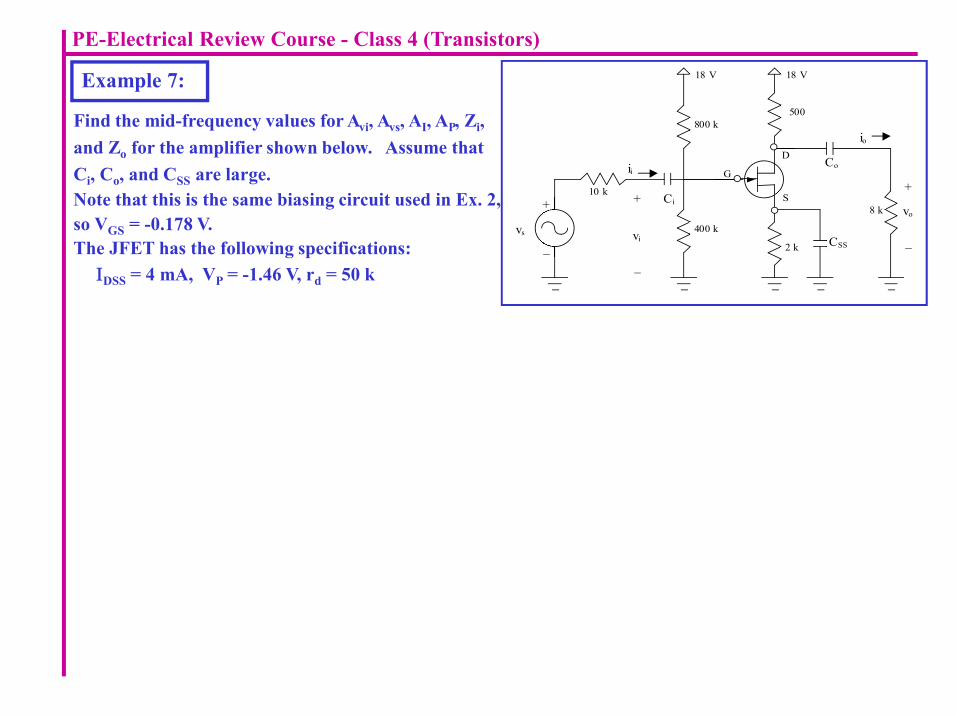
Example 7:
Find the mid-frequency values for Avi, Avs, AI, AP, Zi,
and Zo for the amplifier shown below. Assume that
Ci, Co, and CSS are large.
Note that this is the same biasing circuit used in Ex. 2,
so VGS = -0.178 V.
The JFET has the following specifications:
IDSS = 4 mA, VP = -1.46 V, rd = 50 k
10 k Ci
8 k
Co
CSS vi
vo
+
+
vs
+
_ _
_
io
ii
D
S
G
18 V 18 V
800 k
2 k
500
400 k

FET Amplifier Configurations and
Relationships:
'' ' m L
vi m L m L 'm L
'L d D L d D L SS L
i Th SS Th
m
o d D d D SS
m
i i ivs vi vi vi
s i s i s i
i i iI vi vi vi
L L L
P vi I vi I
CS CG CD
g RA -g R g R
1 g R
R r R R r R R R R
1Z R R R
g
1Z r R r R R
g
Z Z ZA A A A
R + Z R + Z R + Z
Z Z ZA A A A
R R R
A A A A A
vi I
Th 1 2
A A
where R = R R
VCC
RD
S
R2
RSS
Rs Ci
RL
Co
C2
vi vo
+
+
vs
+
_
_ _
io ii
Common Gate (CG) Amplifier
R1
D
G
Note: The biasing circuit is the same for each amp.
Rs Ci
RL
Co
CSS vi
vo
+
+
vs
+
_ _
_
io
ii
D
S
G
VDD
VDD
R1
RSS
RD
R2
Common Source (CS) Amplifier
R s C i
v i
+
v s
+
_
_
i i G
V DD
V DD
R 1
R SS
R 2
Common Drain (CD) Amplifier (also called “source follower”)
R L
C o
v o
+
_
i o
D
S

Figure: Circuit symbol for an enhancement-mode n-channel MOSFET.
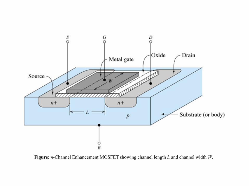
Figure: n-Channel Enhancement MOSFET showing channel length L and channel width W.

Figure: For vGS < Vto the pn junction between drain and body is reverse biased and iD=0.
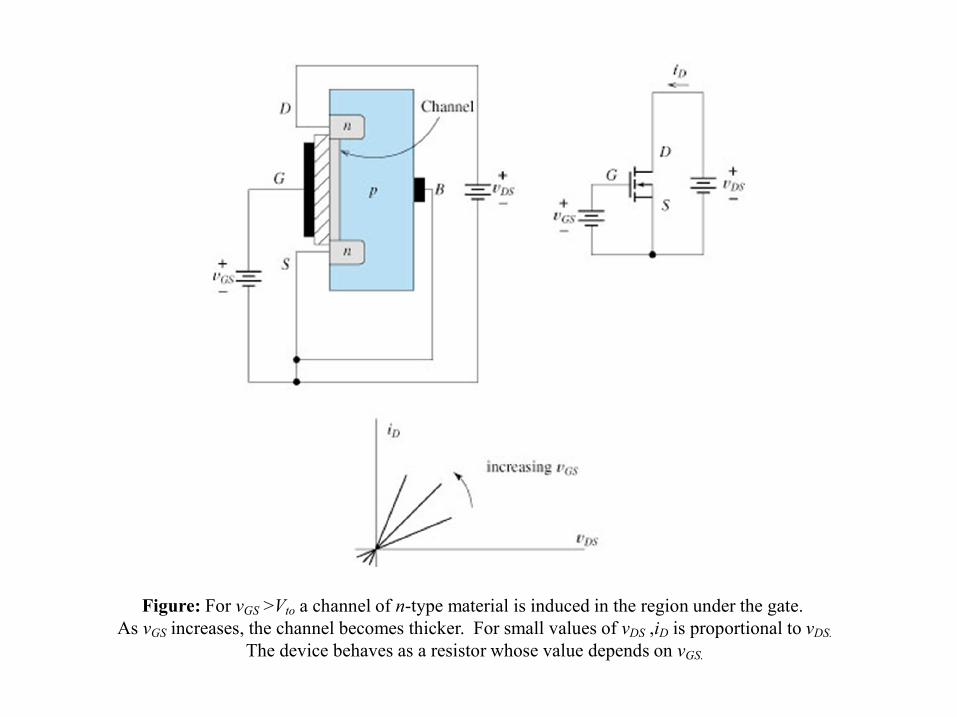
Figure: For vGS >Vto a channel of n-type material is induced in the region under the gate. As vGS increases, the channel becomes thicker. For small values of vDS ,iD is proportional to vDS.
The device behaves as a resistor whose value depends on vGS.

Figure: As vDS increases, the channel pinches down at the drain end and iD increases more slowly. Finally for vDS> vGS -Vto, iD becomes constant.
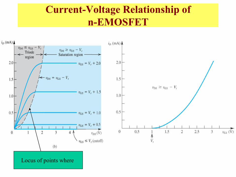
Current-Voltage Relationship of n-EMOSFET
Locus of points where
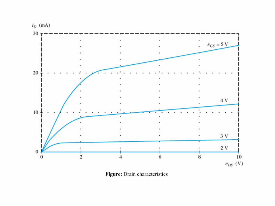
Figure: Drain characteristics
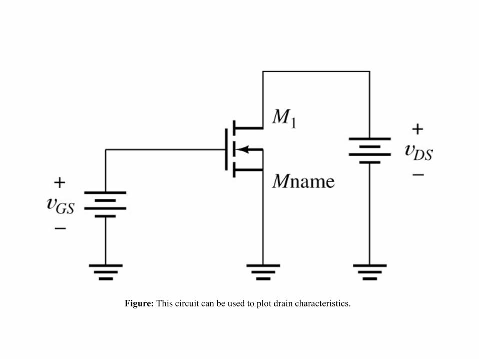
Figure: This circuit can be used to plot drain characteristics.
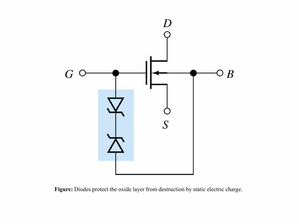
Figure: Diodes protect the oxide layer from destruction by static electric charge.
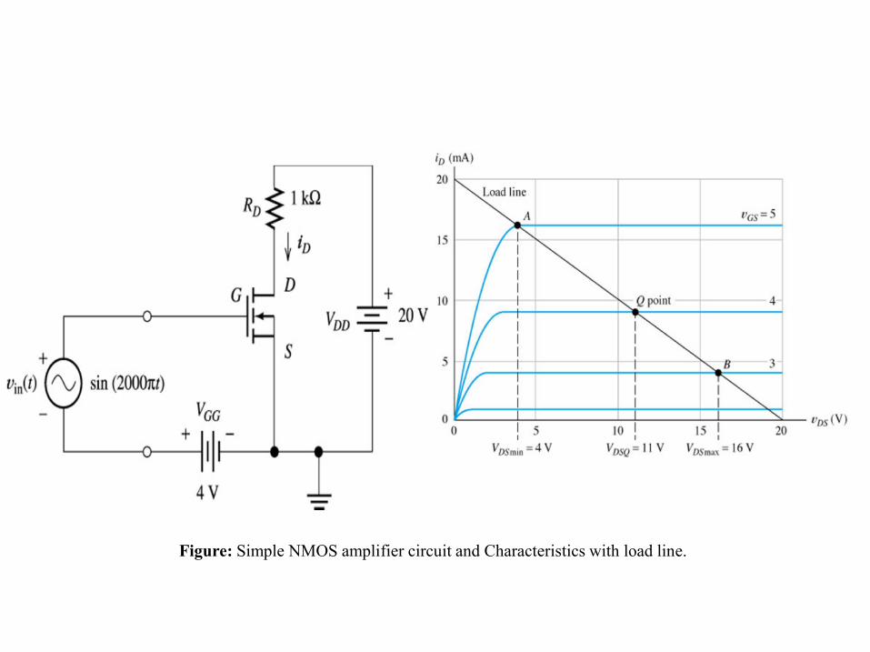
Figure: Simple NMOS amplifier circuit and Characteristics with load line.
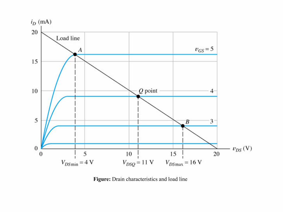
Figure: Drain characteristics and load line
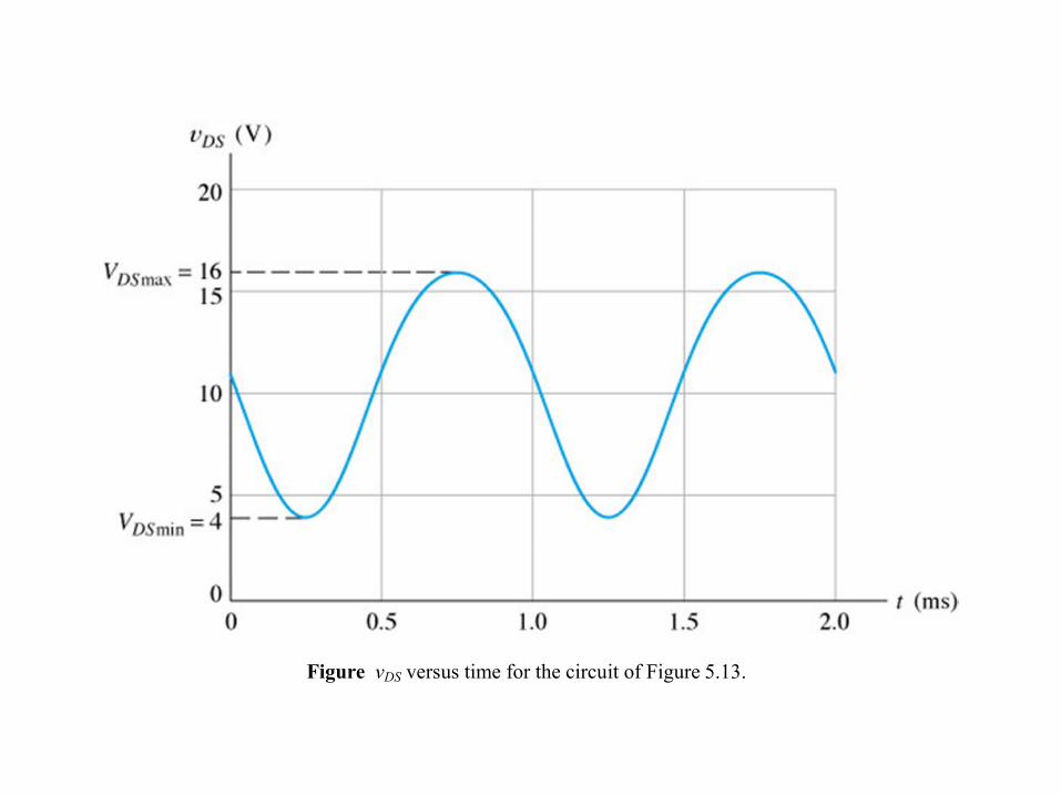
Figure vDS versus time for the circuit of Figure 5.13.
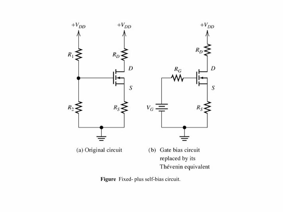
Figure Fixed- plus self-bias circuit.
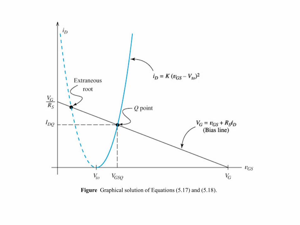
Figure Graphical solution of Equations (5.17) and (5.18).
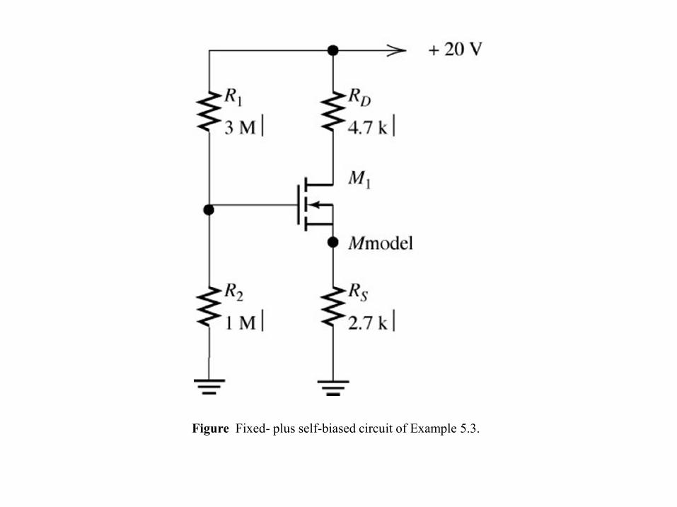
Figure Fixed- plus self-biased circuit of Example 5.3.
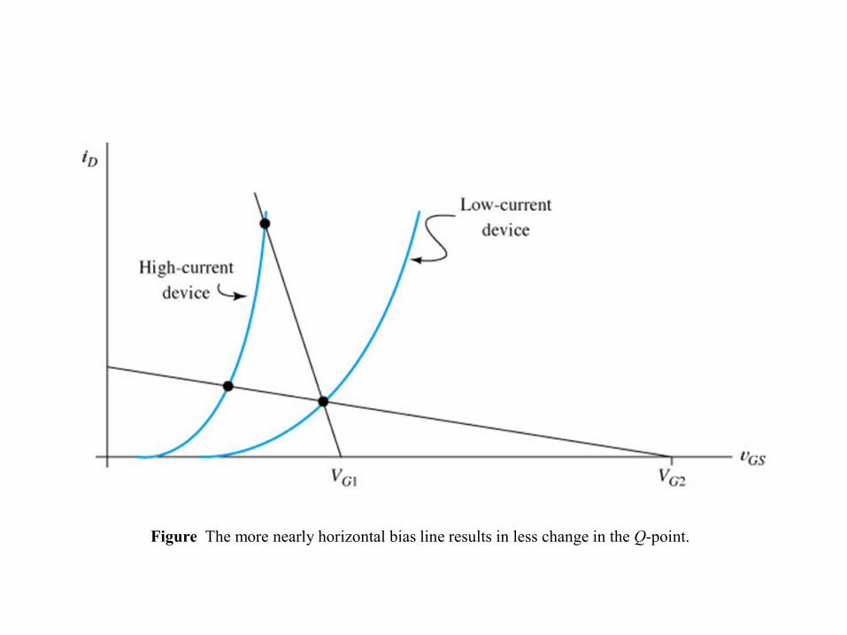
Figure The more nearly horizontal bias line results in less change in the Q-point.
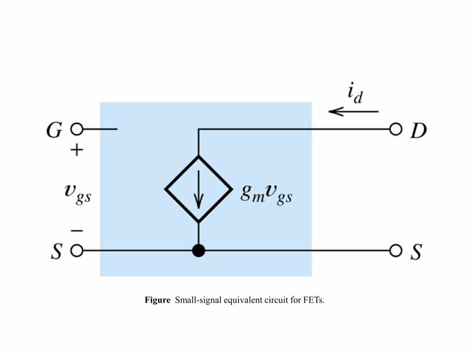
Figure Small-signal equivalent circuit for FETs.
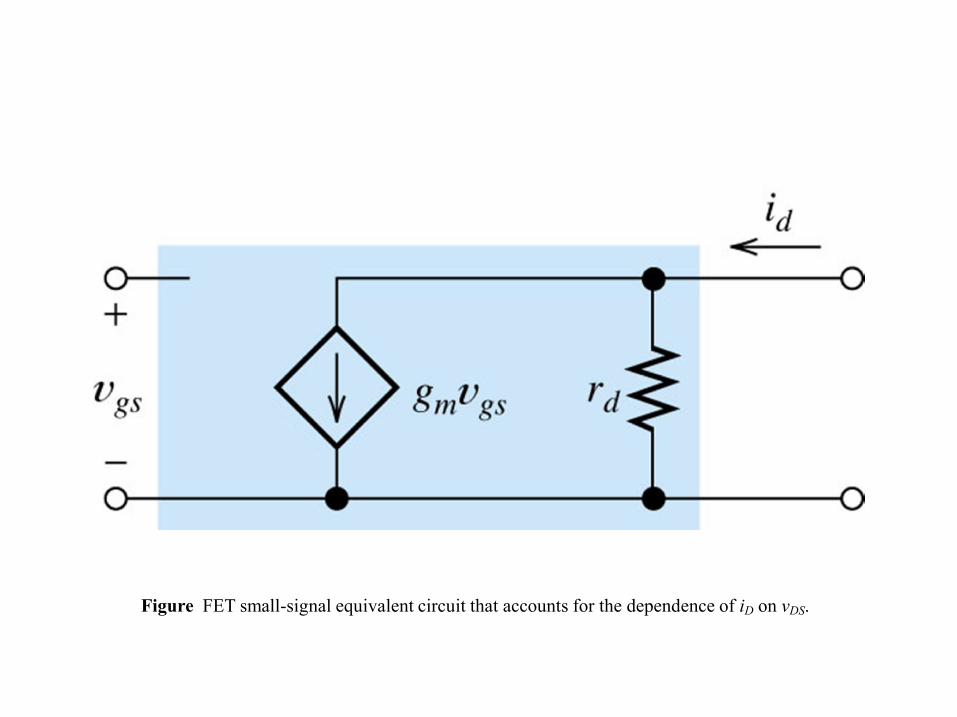
Figure FET small-signal equivalent circuit that accounts for the dependence of iD on vDS.
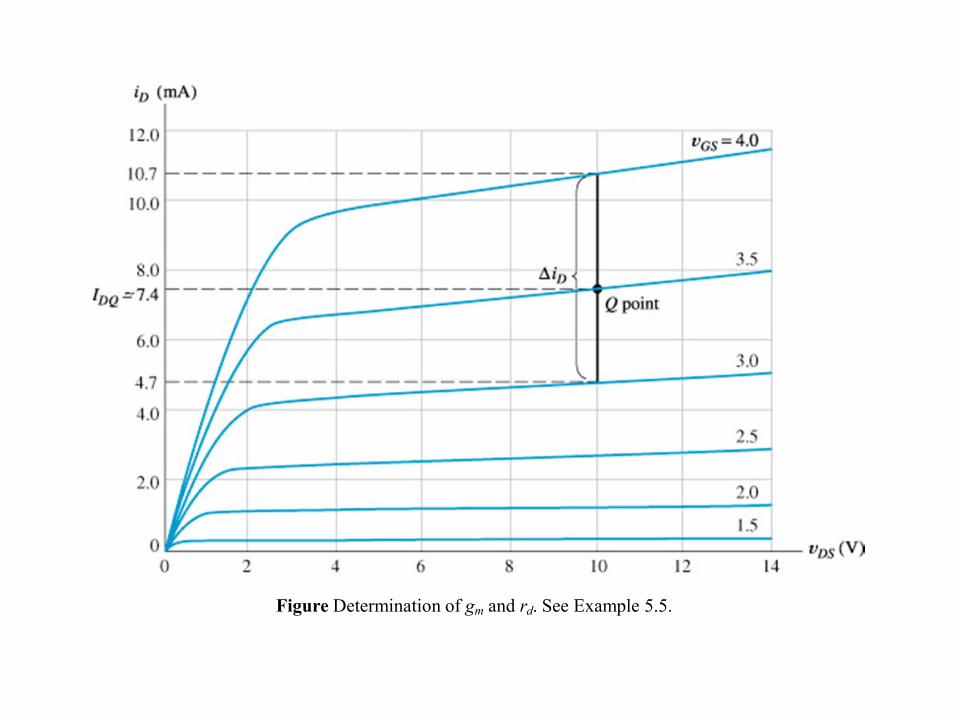
Figure Determination of gm and rd. See Example 5.5.

Figure Common-source amplifier.
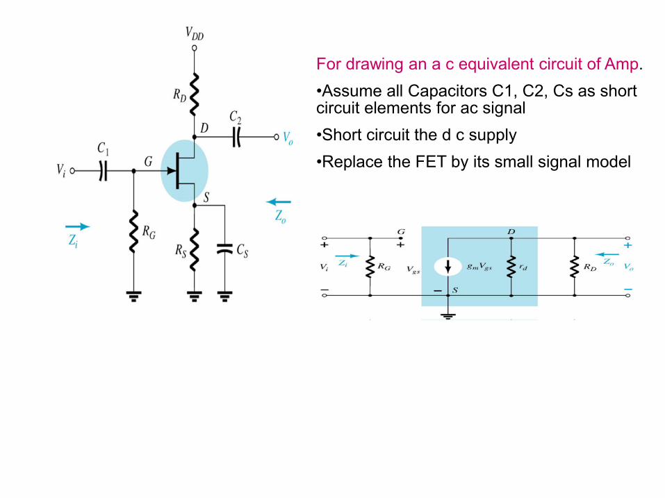
For drawing an a c equivalent circuit of Amp.
•Assume all Capacitors C1, C2, Cs as short circuit elements for ac signal
•Short circuit the d c supply
•Replace the FET by its small signal model
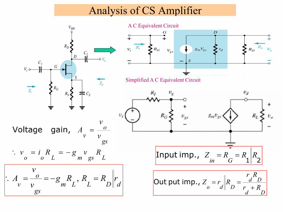
Analysis of CS Amplifier
LgsmLoo
gs
o
v
RvgRiv
v
vA
gain, Voltage
dDLLmgs
o
vrRRRg
v
vA ,
Dd
Dd
Ddo Rr
RrRrZ
imp., put Out
21 imp., Input RRRZ
Gin
A C Equivalent Circuit
Simplified A C Equivalent Circuit
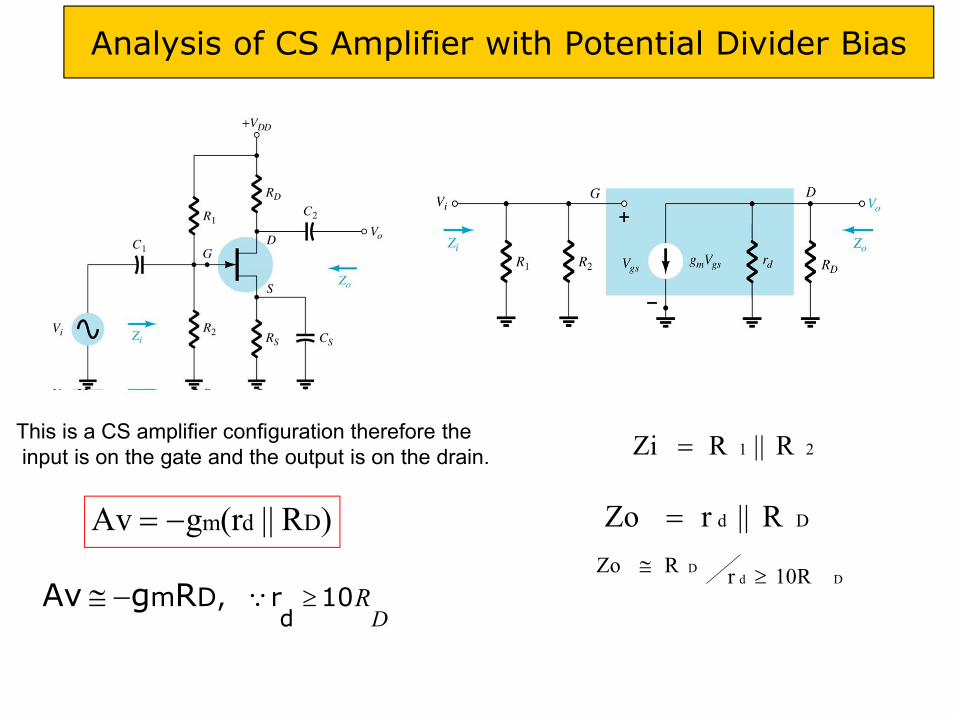
Analysis of CS Amplifier with Potential Divider Bias
)R||(rgAv Ddm
DR10r D,m
dRgAv
)R||(rgAv Ddm
This is a CS amplifier configuration therefore the input is on the gate and the output is on the drain. 21 R||RZi
Dd R||rZo
DdD
10RrRZo

Figure vo(t) and vin(t) versus time for the common-source amplifier of Figure 5.28.
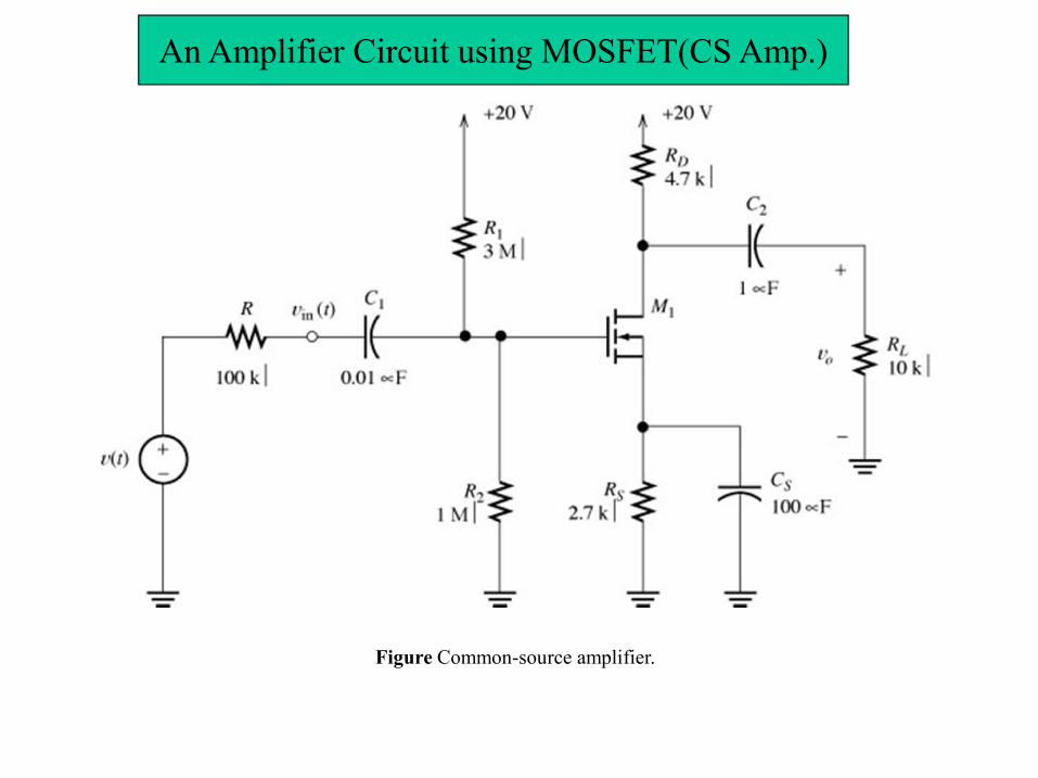
Figure Common-source amplifier.
An Amplifier Circuit using MOSFET(CS Amp.)
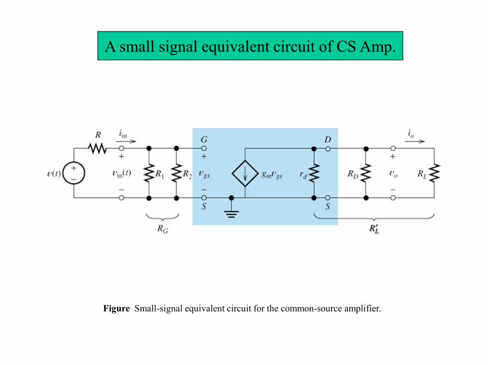
Figure Small-signal equivalent circuit for the common-source amplifier.
A small signal equivalent circuit of CS Amp.
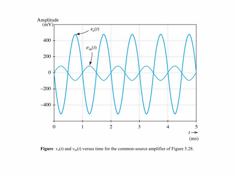
Figure vo(t) and vin(t) versus time for the common-source amplifier of Figure 5.28.
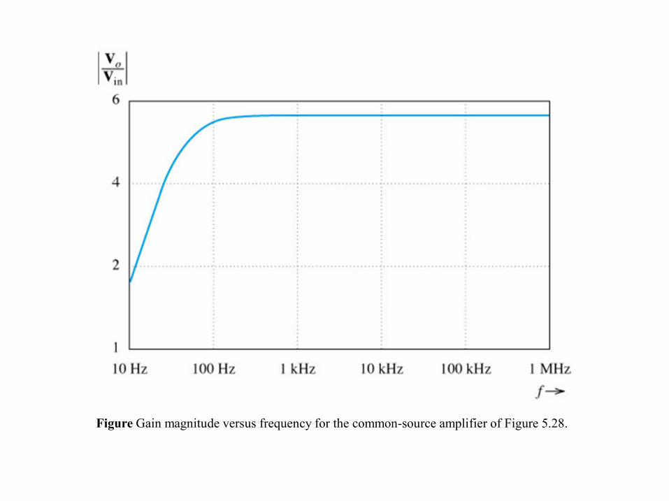
Figure Gain magnitude versus frequency for the common-source amplifier of Figure 5.28.

Figure Source follower.
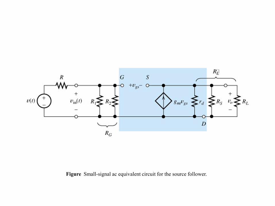
Figure Small-signal ac equivalent circuit for the source follower.

Figure Equivalent circuit used to find the output resistance of the source follower.
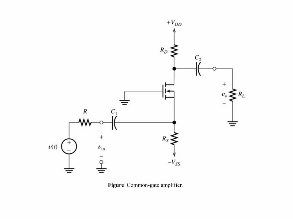
Figure Common-gate amplifier.
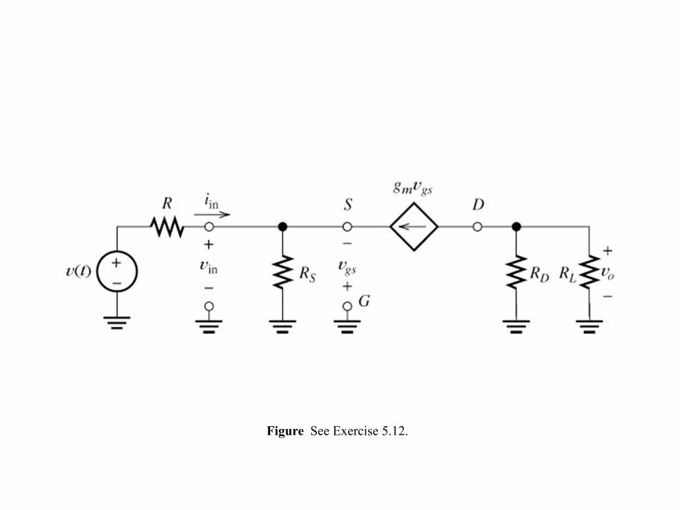
Figure See Exercise 5.12.
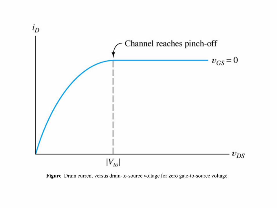
Figure Drain current versus drain-to-source voltage for zero gate-to-source voltage.

Figure n-Channel depletion MOSFET.

Figure Characteristic curves for an NMOS transistor.
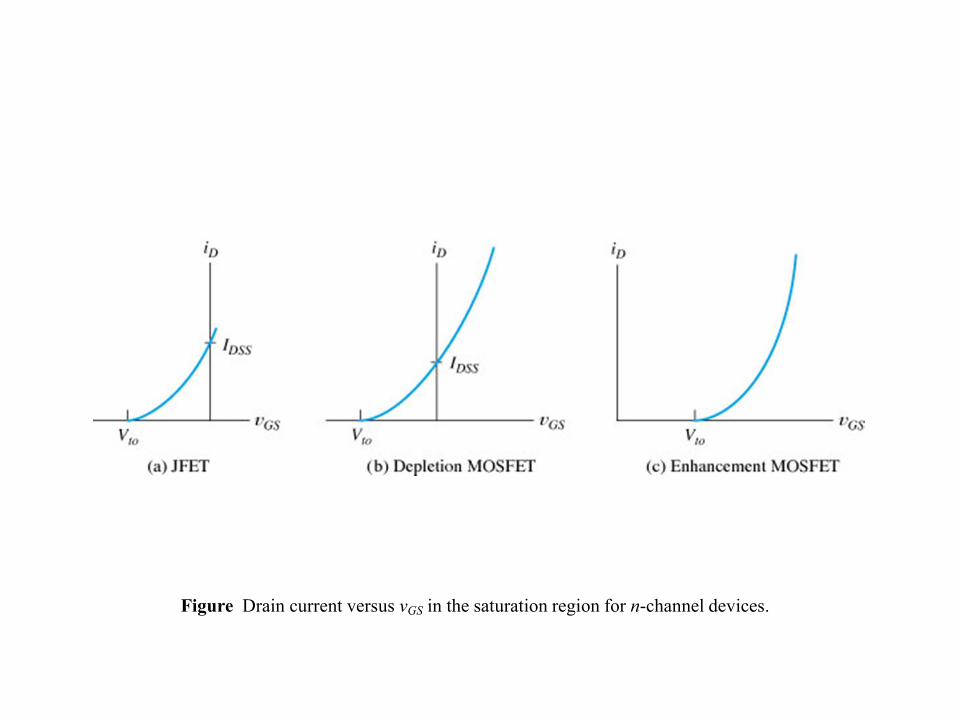
Figure Drain current versus vGS in the saturation region for n-channel devices.
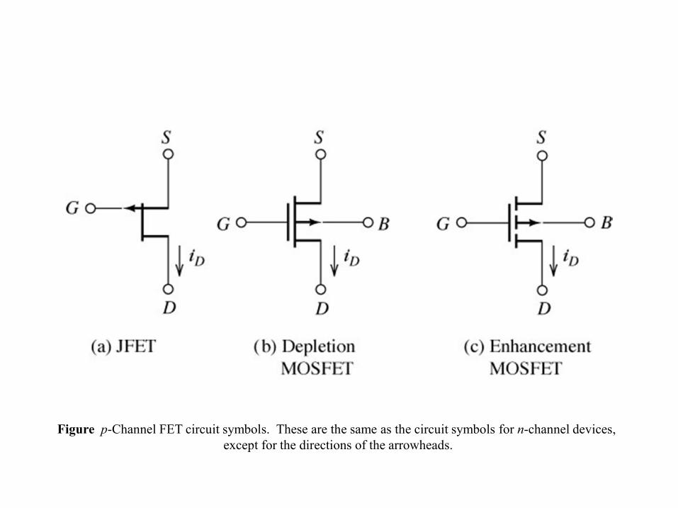
Figure p-Channel FET circuit symbols. These are the same as the circuit symbols for n-channel devices, except for the directions of the arrowheads.
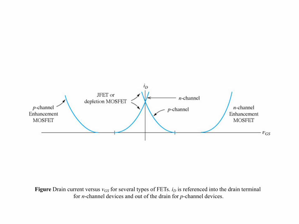
Figure Drain current versus vGS for several types of FETs. iD is referenced into the drain terminal for n-channel devices and out of the drain for p-channel devices.