Femtosecond laser nanomachining initiated by … · a single laser beam and focus it down to...
6
Femtosecond laser nanomachining initiated by ultraviolet multiphoton ionization Xiaoming Yu, 1 Qiumei Bian, 1 Zenghu Chang, 2 P. B. Corkum, 3,4 and Shuting Lei 1,* 1 Industrial and Manufacturing Systems Engineering, Kansas State University, Manhattan, Kansas 66506, USA 2 CREOL and Department of Physics, University of Central Florida Orlando, Florida 32816, USA 3 National Research Council of Canada, Ottawa, Ontario K1A 0R6, Canada 4 University of Ottawa, Ottawa, Ontario K1N 6N5, Canada * [email protected] Abstract: We report on the experimental results of 300 nm features generated on fused silica using a near-infrared (IR) femtosecond laser pulse initiated by an ultraviolet (UV) pulse. With both pulses at a short (~60 fs) delay, the damage threshold of the UV pulse is only 10% of its normal value. Considerable reduction of UV damage threshold is observed when two pulses are at ± 1.3 ps delay. The damage feature size of the combined pulses is similar to that of a single UV pulse. A modified rate equation model with the consideration of defect states is used to help explain these results. This concept can be applied to shorter wavelengths, e.g. XUV and X-ray, with the required fluence below their normal threshold. ©2013 Optical Society of America OCIS codes: (320.2250) Femtosecond phenomena; (240.4350) Nonlinear optics at surfaces; (220.4241) Nanostructure fabrication; (260.7190) Ultraviolet. References and links 1. B. N. Chichkov, C. Momma, S. Nolte, F. von Alvensleben, and A. Tünnermann, “Femtosecond, picosecond and nanosecond laser ablation of solids,” Appl. Phys., A Mater. Sci. Process. 63(2), 109–115 (1996). 2. R. R. Gattass and E. Mazur, “Femtosecond laser micromachining in transparent materials,” Nat. Photonics 2(4), 219–225 (2008). 3. M. Ali, T. Wagner, M. Shakoor, and P. A. Molian, “Review of laser nanomachining,” J. Laser Appl. 20(3), 169– 184 (2008). 4. R. Osellame, H. J. W. M. Hoekstra, G. Cerullo, and M. Pollnau, “Femtosecond laser microstructuring: an enabling tool for optofluidic lab-on-chips,” Laser Photon. Rev. 5(3), 442–463 (2011). 5. A. P. Joglekar, H. H. Liu, E. Meyhöfer, G. Mourou, and A. J. Hunt, “Optics at critical intensity: Applications to nanomorphing,” Proc. Natl. Acad. Sci. U.S.A. 101(16), 5856–5861 (2004). 6. Y. Liao, Y. Shen, L. Qiao, D. Chen, Y. Cheng, K. Sugioka, and K. Midorikawa, “Femtosecond laser nanostructuring in porous glass with sub-50 nm feature sizes,” Opt. Lett. 38(2), 187–189 (2013). 7. S. I. Kudryashov, G. Mourou, A. Joglekar, J. F. Herbstman, and A. J. Hunt, “Nanochannels fabricated by high- intensity femtosecond laser pulses on dielectric surfaces,” Appl. Phys. Lett. 91(14), 141111 (2007). 8. J. M. Fernández-Pradas, C. Florian, F. Caballero-Lucas, J. L. Morenza, and P. Serra, “Femtosecond laser ablation of polymethyl-methacrylate with high focusing control,” Appl. Surf. Sci. 278, 185–189 (2013). 9. D. N. Nikogosyan, M. Dubov, H. Schmitz, V. Mezentsev, I. Bennion, P. Bolger, and A. V. Zayats, “Point-by- point inscription of 250-nm-period structure in bulk fused silica by tightly-focused femtosecond UV pulses: experiment and numerical modeling,” Cent. Eur. J. Phys. 8(2), 169–177 (2010). 10. J. Békési, J. H. Klein-Wiele, and P. Simon, “Efficient submicron processing of metals with femtosecond UV pulses,” Appl. Phys., A Mater. Sci. Process. 76(3), 355–357 (2003). 11. J. Bonse, J. Kruger, S. Hohm, and A. Rosenfeld, “Femtosecond laser-induced periodic surface structures,” J. Laser Appl. 24(4), 042006 (2012). 12. X. Yu, Q. Bian, B. Zhao, Z. Chang, P. B. Corkum, and S. Lei, “Near-infrared femtosecond laser machining initiated by ultraviolet multiphoton ionization,” Appl. Phys. Lett. 102(10), 101111 (2013). 13. B. C. Stuart, M. D. Feit, S. Herman, A. M. Rubenchik, B. W. Shore, and M. D. Perry, “Nanosecond-to- femtosecond laser-induced breakdown in dielectrics,” Phys. Rev. B Condens. Matter 53(4), 1749–1761 (1996). 14. M. Li, S. Menon, J. P. Nibarger, and G. N. Gibson, “Ultrafast Electron Dynamics in Femtosecond Optical Breakdown of Dielectrics,” Phys. Rev. Lett. 82(11), 2394–2397 (1999). 15. D. Grojo, M. Gertsvolf, S. Lei, T. Barillot, D. M. Rayner, and P. B. Corkum, “Exciton-seeded multiphoton ionization in bulk SiO(2),” Phys. Rev. B 81(21), 212301 (2010). 16. P. Martin, S. Guizard, P. Daguzan, G. Petite, P. D'Oliveira, P. Meynadier, and M. Perdrix, “Subpicosecond study of carrier trapping dynamics in wide-band-gap crystals,” Phys. Rev. B 55(9), 5799–5810 (1997). #194597 - $15.00 USD Received 25 Jul 2013; revised 17 Sep 2013; accepted 21 Sep 2013; published 2 Oct 2013 (C) 2013 OSA 7 October 2013 | Vol. 21, No. 20 | DOI:10.1364/OE.21.024185 | OPTICS EXPRESS 24185
Transcript of Femtosecond laser nanomachining initiated by … · a single laser beam and focus it down to...

Femtosecond laser nanomachining initiated by ultraviolet multiphoton ionization
Xiaoming Yu,1 Qiumei Bian,1 Zenghu Chang,2 P. B. Corkum,3,4 and Shuting Lei1,* 1Industrial and Manufacturing Systems Engineering, Kansas State University, Manhattan, Kansas 66506, USA
2CREOL and Department of Physics, University of Central Florida Orlando, Florida 32816, USA 3National Research Council of Canada, Ottawa, Ontario K1A 0R6, Canada
4University of Ottawa, Ottawa, Ontario K1N 6N5, Canada *[email protected]
Abstract: We report on the experimental results of 300 nm features generated on fused silica using a near-infrared (IR) femtosecond laser pulse initiated by an ultraviolet (UV) pulse. With both pulses at a short (~60 fs) delay, the damage threshold of the UV pulse is only 10% of its normal value. Considerable reduction of UV damage threshold is observed when two pulses are at ± 1.3 ps delay. The damage feature size of the combined pulses is similar to that of a single UV pulse. A modified rate equation model with the consideration of defect states is used to help explain these results. This concept can be applied to shorter wavelengths, e.g. XUV and X-ray, with the required fluence below their normal threshold.
©2013 Optical Society of America
OCIS codes: (320.2250) Femtosecond phenomena; (240.4350) Nonlinear optics at surfaces; (220.4241) Nanostructure fabrication; (260.7190) Ultraviolet.
References and links 1. B. N. Chichkov, C. Momma, S. Nolte, F. von Alvensleben, and A. Tünnermann, “Femtosecond, picosecond and
nanosecond laser ablation of solids,” Appl. Phys., A Mater. Sci. Process. 63(2), 109–115 (1996). 2. R. R. Gattass and E. Mazur, “Femtosecond laser micromachining in transparent materials,” Nat. Photonics 2(4),
219–225 (2008). 3. M. Ali, T. Wagner, M. Shakoor, and P. A. Molian, “Review of laser nanomachining,” J. Laser Appl. 20(3), 169–
184 (2008). 4. R. Osellame, H. J. W. M. Hoekstra, G. Cerullo, and M. Pollnau, “Femtosecond laser microstructuring: an
enabling tool for optofluidic lab-on-chips,” Laser Photon. Rev. 5(3), 442–463 (2011). 5. A. P. Joglekar, H. H. Liu, E. Meyhöfer, G. Mourou, and A. J. Hunt, “Optics at critical intensity: Applications to
nanomorphing,” Proc. Natl. Acad. Sci. U.S.A. 101(16), 5856–5861 (2004). 6. Y. Liao, Y. Shen, L. Qiao, D. Chen, Y. Cheng, K. Sugioka, and K. Midorikawa, “Femtosecond laser
nanostructuring in porous glass with sub-50 nm feature sizes,” Opt. Lett. 38(2), 187–189 (2013). 7. S. I. Kudryashov, G. Mourou, A. Joglekar, J. F. Herbstman, and A. J. Hunt, “Nanochannels fabricated by high-
intensity femtosecond laser pulses on dielectric surfaces,” Appl. Phys. Lett. 91(14), 141111 (2007). 8. J. M. Fernández-Pradas, C. Florian, F. Caballero-Lucas, J. L. Morenza, and P. Serra, “Femtosecond laser
ablation of polymethyl-methacrylate with high focusing control,” Appl. Surf. Sci. 278, 185–189 (2013). 9. D. N. Nikogosyan, M. Dubov, H. Schmitz, V. Mezentsev, I. Bennion, P. Bolger, and A. V. Zayats, “Point-by-
point inscription of 250-nm-period structure in bulk fused silica by tightly-focused femtosecond UV pulses: experiment and numerical modeling,” Cent. Eur. J. Phys. 8(2), 169–177 (2010).
10. J. Békési, J. H. Klein-Wiele, and P. Simon, “Efficient submicron processing of metals with femtosecond UV pulses,” Appl. Phys., A Mater. Sci. Process. 76(3), 355–357 (2003).
11. J. Bonse, J. Kruger, S. Hohm, and A. Rosenfeld, “Femtosecond laser-induced periodic surface structures,” J. Laser Appl. 24(4), 042006 (2012).
12. X. Yu, Q. Bian, B. Zhao, Z. Chang, P. B. Corkum, and S. Lei, “Near-infrared femtosecond laser machining initiated by ultraviolet multiphoton ionization,” Appl. Phys. Lett. 102(10), 101111 (2013).
13. B. C. Stuart, M. D. Feit, S. Herman, A. M. Rubenchik, B. W. Shore, and M. D. Perry, “Nanosecond-to-femtosecond laser-induced breakdown in dielectrics,” Phys. Rev. B Condens. Matter 53(4), 1749–1761 (1996).
14. M. Li, S. Menon, J. P. Nibarger, and G. N. Gibson, “Ultrafast Electron Dynamics in Femtosecond Optical Breakdown of Dielectrics,” Phys. Rev. Lett. 82(11), 2394–2397 (1999).
15. D. Grojo, M. Gertsvolf, S. Lei, T. Barillot, D. M. Rayner, and P. B. Corkum, “Exciton-seeded multiphoton ionization in bulk SiO(2),” Phys. Rev. B 81(21), 212301 (2010).
16. P. Martin, S. Guizard, P. Daguzan, G. Petite, P. D'Oliveira, P. Meynadier, and M. Perdrix, “Subpicosecond study of carrier trapping dynamics in wide-band-gap crystals,” Phys. Rev. B 55(9), 5799–5810 (1997).
#194597 - $15.00 USD Received 25 Jul 2013; revised 17 Sep 2013; accepted 21 Sep 2013; published 2 Oct 2013(C) 2013 OSA 7 October 2013 | Vol. 21, No. 20 | DOI:10.1364/OE.21.024185 | OPTICS EXPRESS 24185

17. G. M. Petrov and J. Davis, “Interaction of intense ultra-short laser pulses with dielectrics,” J. Phys. B 41(2), 025601 (2008).
18. J. Peng, D. Grojo, D. M. Rayner, and P. B. Corkum, “Control of energy deposition in femtosecond laser dielectric interactions,” Appl. Phys. Lett. 102(16), 161105 (2013).
19. Y. Wu, E. Cunningham, H. Zang, J. Li, M. Chini, X. Wang, Y. Wang, K. Zhao, and Z. Chang, “Generation of high-flux attosecond extreme ultraviolet continuum with a 10 TW laser,” Appl. Phys. Lett. 102(20), 201104 (2013).
1. Introduction
Direct fabrication of nanoscale structures in at least one dimension is of significant importance for miniaturization and integration. Although photolithography is commonly used in industry and structures of several tens of nanometers can be achieved, single-step nanomachining methods are still desired. Ultrafast lasers are a promising tool for nanomachining due to the unique properties such as reduced thermal effects and the potential for direct 3-dimensional fabrication [1–3]. Waveguides, microfluidic devices, opto-electronic systems have been successfully fabricated using femtosecond lasers [4].
Generally speaking, there are two approaches to direct laser nanomachining. One is to use a single laser beam and focus it down to sub-micrometer scale using high numerical aperture focusing optics. Due to the nonlinear interaction between ultrafast laser pulses and wide bandgap dielectric materials, further reduction of damage size is possible by setting the pulse energy such that only the center part of the focused beam is above the damage threshold. By this means, small features with dimension of ~40 nm are achieved with 800 nm wavelength pulses [5,6]. However, this method requires a very high degree of laser power stability and thus is not practical for industrial applications. Due to diffraction limit of all focused laser beams, the minimal focal spot size is of the order of λ/NA, where λ is laser wavelength and NA is the numerical aperture of focusing optics. One way to reduce focal size is using high NA microscope objectives. By using high NA objectives, structures with the size of ~130 nm and 200 nm are achieved on the surface of fused silica [7] and PMMA [8], respectively. Alternatively, by using short wavelength laser beams, such as UV lasers with wavelength of 200-400 nm and proper focusing, structures of 250 nm on fused silica [9] and 600 nm on stainless steel foils [10] are achieved.
The other approach is to use multiple laser beams and usually the interference between these beams are utilized, e.g., laser-induced periodic surface structures (LIPSS) [11], which is beyond the scope of our research.
As mentioned above, one effective way to reduce focal spot size is to use short wavelength beams, such as XUV and X-ray, generated from high harmonic generation (HHG). However, due to the low conversion efficiency of HHG, direct machining of dielectrics using HHG remains a challenge. Our recent results show that with the help of a long wavelength IR beam, the damage threshold of 267 nm beam is lowed by 88% [12]. This provides a pathway to XUV or even shorter wavelength laser nanomachining with energy below the damage threshold.
In this paper, we present a novel approach for laser direct fabrication of nanostructures in which 267 nm femtosecond laser pulses are used to produce seed electrons with subsequent damage induced by IR pulses. The significance of this approach is its potential downward scalability in feature size with shorter and shorter wavelengths down to sub 10 nm.
#194597 - $15.00 USD Received 25 Jul 2013; revised 17 Sep 2013; accepted 21 Sep 2013; published 2 Oct 2013(C) 2013 OSA 7 October 2013 | Vol. 21, No. 20 | DOI:10.1364/OE.21.024185 | OPTICS EXPRESS 24186
2. Experimental details
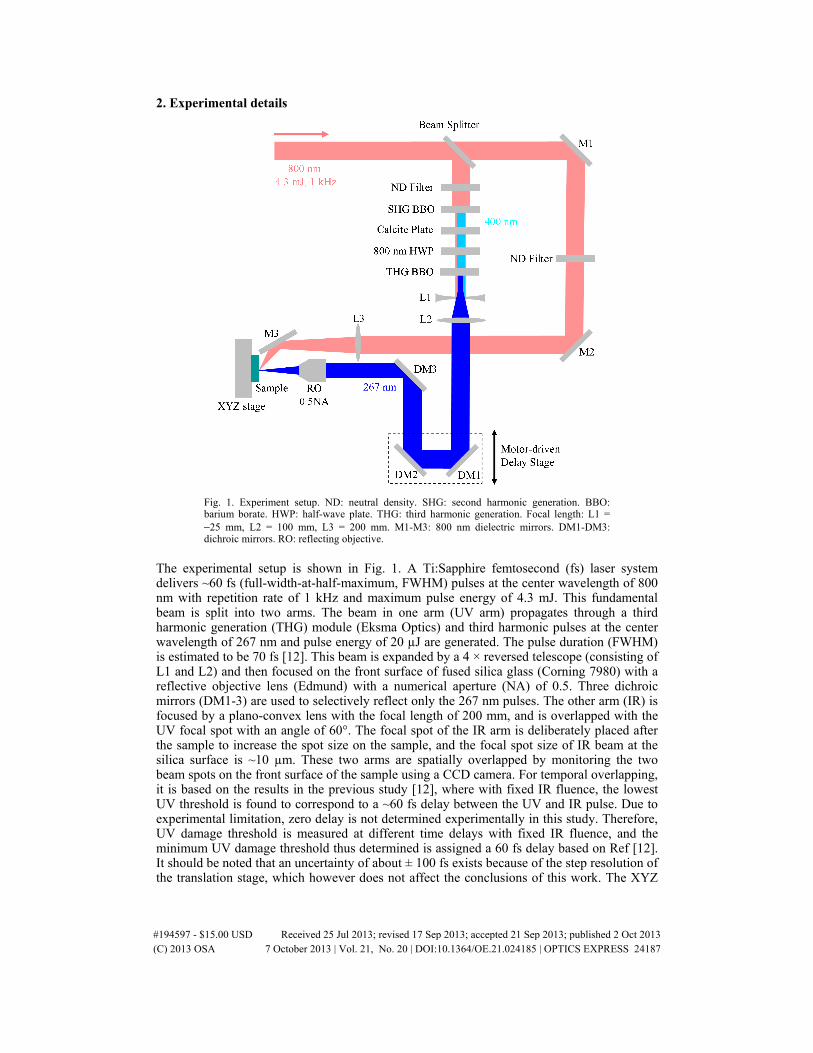
Fig. 1. Experiment setup. ND: neutral density. SHG: second harmonic generation. BBO: barium borate. HWP: half-wave plate. THG: third harmonic generation. Focal length: L1 = −25 mm, L2 = 100 mm, L3 = 200 mm. M1-M3: 800 nm dielectric mirrors. DM1-DM3: dichroic mirrors. RO: reflecting objective.
The experimental setup is shown in Fig. 1. A Ti:Sapphire femtosecond (fs) laser system delivers ~60 fs (full-width-at-half-maximum, FWHM) pulses at the center wavelength of 800 nm with repetition rate of 1 kHz and maximum pulse energy of 4.3 mJ. This fundamental beam is split into two arms. The beam in one arm (UV arm) propagates through a third harmonic generation (THG) module (Eksma Optics) and third harmonic pulses at the center wavelength of 267 nm and pulse energy of 20 µJ are generated. The pulse duration (FWHM) is estimated to be 70 fs [12]. This beam is expanded by a 4 × reversed telescope (consisting of L1 and L2) and then focused on the front surface of fused silica glass (Corning 7980) with a reflective objective lens (Edmund) with a numerical aperture (NA) of 0.5. Three dichroic mirrors (DM1-3) are used to selectively reflect only the 267 nm pulses. The other arm (IR) is focused by a plano-convex lens with the focal length of 200 mm, and is overlapped with the UV focal spot with an angle of 60°. The focal spot of the IR arm is deliberately placed after the sample to increase the spot size on the sample, and the focal spot size of IR beam at the silica surface is ~10 µm. These two arms are spatially overlapped by monitoring the two beam spots on the front surface of the sample using a CCD camera. For temporal overlapping, it is based on the results in the previous study [12], where with fixed IR fluence, the lowest UV threshold is found to correspond to a ~60 fs delay between the UV and IR pulse. Due to experimental limitation, zero delay is not determined experimentally in this study. Therefore, UV damage threshold is measured at different time delays with fixed IR fluence, and the minimum UV damage threshold thus determined is assigned a 60 fs delay based on Ref [12]. It should be noted that an uncertainty of about ± 100 fs exists because of the step resolution of the translation stage, which however does not affect the conclusions of this work. The XYZ
#194597 - $15.00 USD Received 25 Jul 2013; revised 17 Sep 2013; accepted 21 Sep 2013; published 2 Oct 2013(C) 2013 OSA 7 October 2013 | Vol. 21, No. 20 | DOI:10.1364/OE.21.024185 | OPTICS EXPRESS 24187
stage is moving at a constant speed of 50 mm/s, resulting in a 50 μm separation between the laser shots. This ensures that each pulse irradiates at a fresh site on the sample.
3. Results and discussion
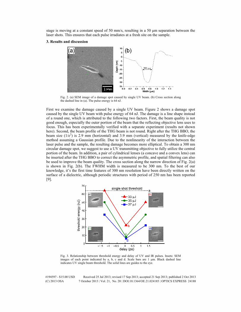
Fig. 2. (a) SEM image of a damage spot caused by single UV beam. (b) Cross section along the dashed line in (a). The pulse energy is 64 nJ.
First we examine the damage caused by a single UV beam. Figure 2 shows a damage spot caused by the single UV beam with pulse energy of 64 nJ. The damage is a line shape instead of a round one, which is attributed to the following two factors. First, the beam quality is not good enough, especially the outer portion of the beam that the reflecting objective lens uses to focus. This has been experimentally verified with a separate experiment (results not shown here). Second, the beam profile of the THG beam is not round. Right after the THG BBO, the beam size (1/e2) is 2.9 mm (horizontal) and 3.9 mm (vertical) measured by the knife-edge method assuming a Gaussian profile. Due to the nonlinearity of the interaction between the laser pulse and the sample, the resulting damage becomes more elliptical. To obtain a 300 nm circular damage spot, we suggest to use a UV transmitting objective to fully utilize the central portion of the beam. In addition, a pair of cylindrical lenses (a concave and a convex lens) can be inserted after the THG BBO to correct the asymmetric profile, and spatial filtering can also be used to improve the beam quality. The cross section along the narrow direction of Fig. 2(a) is shown in Fig. 2(b). The FWHM width is measured to be 300 nm. To the best of our knowledge, it’s the first time features of 300 nm resolution have been directly written on the surface of a dielectric, although periodic structures with period of 250 nm has been reported [9].
Fig. 3. Relationship between threshold energy and delay of UV and IR pulses. Insets: SEM images of each point indicated by a, b, c and d. Scale bars are 1 μm. Black dashed line indicates UV single beam threshold. The solid lines are guides to the eye.
#194597 - $15.00 USD Received 25 Jul 2013; revised 17 Sep 2013; accepted 21 Sep 2013; published 2 Oct 2013(C) 2013 OSA 7 October 2013 | Vol. 21, No. 20 | DOI:10.1364/OE.21.024185 | OPTICS EXPRESS 24188
With the combination of UV and IR beams, the damage threshold of UV beam can be lowered by ~90%, as shown in Fig. 3. Three IR energy levels (33 μJ, 35 μJ, 37 μJ) and three delays (−1.3 ps, 60 fs, 1.3 ps) are used. Positive delays are defined as when the UV pulse reaches the sample before the IR pulse. In the experiments, different UV energy is used and the damage threshold is determined as the lowest energy with which nanoscale damage is observed using SEM. No damage is seen using only the IR beam. As can be seen in Fig. 3, at 60 fs delay and 37 μJ IR energy, UV damage threshold is ~10% of the normal value, and it increases with longer delays and with lower IR energy. This feature is observed in our recent experiments [12]. In contrast to the multiple shot threshold, this time we used single shot threshold measurement to avoid incubation effects. It should be noted that at 60 fs delay, the damage threshold using IR energy of 37 μJ and 35 μJ is similar. This is because 6 nJ is the lowest energy level that can be measured accurately due to background noise. Therefore, the actual damage threshold using IR energy of 37 μJ may be lower than 6 nJ. The insets show SEM images of the points indicated by the corresponding letters. As can be seen, the feature size is similar for different cases, which suggests that this technique can be used for nanomachining with an XUV (or shorter wavelength) beam combined with a longer wavelength beam, and the resulting feature size is only determined by the XUV beam. It should be noted that with the combination of two beams, there is an increase of edge roughness in morphology (Figs. 3(b)-3(d)) compared to the damage caused by single UV beam (Fig. 3(a)), which may be caused by the energy fluctuation of the UV beam, especially when the pulse energy is low.
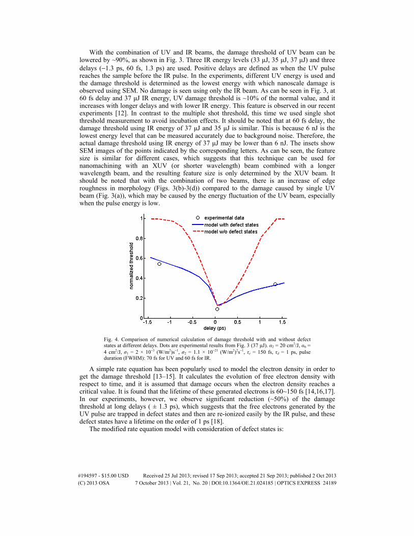
Fig. 4. Comparison of numerical calculation of damage threshold with and without defect states at different delays. Dots are experimental results from Fig. 3 (37 μJ). α2 = 20 cm2/J, α6 = 4 cm2/J, σ1 = 2 × 10⁻³ (W/m2)s−1, σ2 = 1.1 × 10⁻²¹ (W/m2)2s−1, τe = 150 fs, τd = 1 ps, pulse duration (FWHM): 70 fs for UV and 60 fs for IR.
A simple rate equation has been popularly used to model the electron density in order to get the damage threshold [13–15]. It calculates the evolution of free electron density with respect to time, and it is assumed that damage occurs when the electron density reaches a critical value. It is found that the lifetime of these generated electrons is 60~150 fs [14,16,17]. In our experiments, however, we observe significant reduction (~50%) of the damage threshold at long delays ( ± 1.3 ps), which suggests that the free electrons generated by the UV pulse are trapped in defect states and then are re-ionized easily by the IR pulse, and these defect states have a lifetime on the order of 1 ps [18].
The modified rate equation model with consideration of defect states is:
#194597 - $15.00 USD Received 25 Jul 2013; revised 17 Sep 2013; accepted 21 Sep 2013; published 2 Oct 2013(C) 2013 OSA 7 October 2013 | Vol. 21, No. 20 | DOI:10.1364/OE.21.024185 | OPTICS EXPRESS 24189

( ) je eMPI e j d
e
jd e dj d
e d
dn nW I In I ndtdn n nI ndt
α στ
στ τ
= + + −
= − − (1)
where ne is free electron density, WMPI is the Keldysh multi-photon ionization rate, I is laser intensity, α and σ are the ionization cross section of avalanche electrons and defect states, respectively, τe and τd are decay time of free electrons and defect states, respectively, and nd is defect state density. We use j = 1 and 2 for UV and IR beams respectively [15]. Both UV and IR pulses have a Gaussian shape in time and the pulse duration (FWHM) is 70 fs and 60 fs, respectively. In our model, free electrons are first generated by photo-ionization (calculated by the Keldysh theory) and the electron density is further increased by avalanche ionization within the pulse duration. The decay time of these electrons is 150 fs and all of them are assumed to decay into defect states which have a bandgap of 3.2 eV. It should be noted that in this model the defect states have a single band lying in between the conduction band and exciton band [15]. The second pulse re-ionizes the defect states to free electrons, and both photo and avalanche ionization are also considered. Damage occurs when free electron density reaches 1.7 × 1021 cm−3 (critical density at 800 nm wavelength).
The modeling results and experimental data (37 μJ, Fig. 3) are shown in Fig. 4, and for comparison, modeling results using the same parameters without the defect states term is also shown. As can be seen, our model agrees with the experimental data well with the defect states term considered, and the lifetime of defect states is found to be ~1 ps, which is similar to recent results [18]. Without defect states, the damage threshold will return to its normal value at much shorter delays because the electrons have a shorter lifetime.
4. Conclusion
Using a high NA objective to focus a UV femtosecond laser beam, nanostructures with dimension of 300 nm are fabricated on the surface of fused silica. The damage threshold of the UV beam can be reduced by ~90% with the combination of an IR beam at short (~60 fs) delay. The required seeding pulse energy can already be reached in the XUV wavelength range by high harmonic generation [19]. Significant UV threshold reduction at ± 1.3 ps indicates that defect states, which have a longer lifetime compared to free electrons, should be taken into account. Our modified rate equation model confirms the role of defect states.
Acknowledgments
Xiaoming Yu, Qiumei Bian and Shuting Lei acknowledge the support from the National Science Foundation. Zenghu Chang acknowledges the support from the US Army Research Office.
#194597 - $15.00 USD Received 25 Jul 2013; revised 17 Sep 2013; accepted 21 Sep 2013; published 2 Oct 2013(C) 2013 OSA 7 October 2013 | Vol. 21, No. 20 | DOI:10.1364/OE.21.024185 | OPTICS EXPRESS 24190