Femtosecond-laser Microstructuring ... - Projects at Harvard
INDUSTRIAL LASERAPPLICATIONS LABAPPLICATION FOCUS
Femtosecond Laser Irradiation and Chemical Etching (FLICE); Waveguide WritingMicrofabrication technologies have miniaturised many fields, from microelectronics to photonics, paving the way for a wide range of new applications. In particular, the capability of realising microfluidic channels has revolutionised the field of optofluidics.
Microfluidic channels and patterns are typically fabricated by lithographic and chemical-etching techniques, but these approaches are primarily limited to the fabrication of two-dimensional patterns on the surface. Indeed, in order to create a true 3-D structure several layers of glass substrates need to be patterned, etched and fused together.
Femtosecond Laser Irradiation and Chemical Etching (FLICE) allows 3-D micromachining, thus permitting the direct fabrication of buried microchannels with various aspect ratios and patterns.
Being a maskless technology, it enables rapid low-cost prototyping of new devices. Moreover, since the same femtosecond laser can be used to produce low loss optical waveguides in a 3-D geometry, these femtosecond laser based technologies could become a single solution for fabrication of microfluidic channels and their integration with optical circuits.
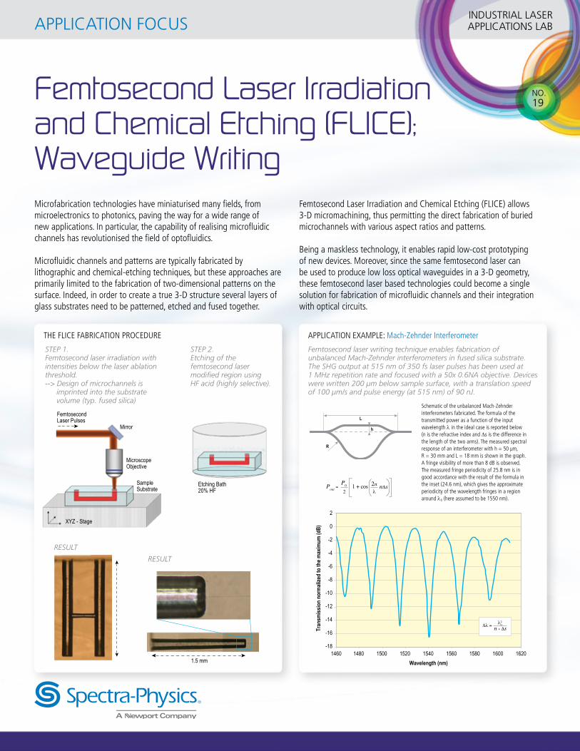
STEP 1.Femtosecond laser irradiation with intensities below the laser ablation threshold.--> Design of microchannels is
imprinted into the substrate volume (typ. fused silica)
RESULT
STEP 2.Etching of the femtosecond laser modified region using HF acid (highly selective).
RESULT
NO.19
THE FLICE FABRICATION PROCEDURE APPLICATION EXAMPLE: Mach-Zehnder Interferometer
Mirror
MicroscopeObjective
SampleSubstrate
XYZ - Stage
Femtosecond Laser Pulses
Etching Bath20% HF
1.5 mm
L
h
R
Pout = 1 + cos nΔsλ
2π
2
P0
2
0
-2
-4
-6
-8
-10
-12
-14
-16
-181460 1480 1500 1520 1540 1560 1580 1600 1620
Wavelength (nm)
Tran
smis
sion
nor
mal
ized
to th
e m
axim
um (d
B)
Δλ = λ2
0
n . Δs
Schematic of the unbalanced Mach-Zehnder interferometers fabricated. The formula of the transmitted power as a function of the input wavelength l in the ideal case is reported below (n is the refractive index and Δs is the difference in the length of the two arms). The measured spectral response of an interferometer with h = 50 µm, R = 30 mm and L = 18 mm is shown in the graph. A fringe visibility of more than 8 dB is observed. The measured fringe periodicity of 25.8 nm is in good accordance with the result of the formula in the inset (24.6 nm), which gives the approximate periodicity of the wavelength fringes in a region around l0 (here assumed to be 1550 nm).
Femtosecond laser writing technique enables fabrication of unbalanced Mach-Zehnder interferometers in fused silica substrate. The SHG output at 515 nm of 350 fs laser pulses has been used at 1 MHz repetition rate and focused with a 50x 0.6NA objective. Devices were written 200 µm below sample surface, with a translation speed of 100 µm/s and pulse energy (at 515 nm) of 90 nJ.
Femtosecond Laser Irradiation and Chemical Etching (FLICE); Waveguide Writing
© 2015 Newport Corporation. All Rights Reserved. Spectra-Physics and the Spectra-Physics logo are registered trademarks of Newport Corporation. Spectra-Physics Santa Clara, California, Stahnsdorf, Germany, Rankweil, Austria and Tel Aviv, Israel have all been certified compliant with ISO 9001.
ACKNOWLEDGEMENTS: This work was performed at the Dipartimento di Fisica, Politecnico di Milano, Piazza L. da Vinci 32 20133 Milano, Italy | Roberto Osellame, Giulio Cerullo | Tel. +39-02-23996164 Fax +39-02-23996126 | E-mail: [email protected], [email protected] | http://www.cusbo.polimi.it. This work was supported by the European Commission (STREP EU: FP6 IST-2005-034562, “HIBISCUS”)
3635 Peterson Way, Santa Clara, CA 95054, USAPHONE: 1-800-775-5273 1-408-980-4300 FAX: 1-408-980-6921 EMAIL: [email protected]
www.spectra-physics.com
China +86-10-6267-0065 [email protected] +33-(0)1-60-91-68-68 [email protected] +81-3-3794-5511 [email protected] +886 -(0)2-2508-4977 [email protected] +65-6664-0400 [email protected]
Belgium +32-(0)0800-11 257 [email protected] +31-(0)30 6592111 [email protected] Kingdom +44-1235-432-710 [email protected] / Austria / Switzerland +49-(0)6151-708-0 [email protected]
SP-DS-20150113-8
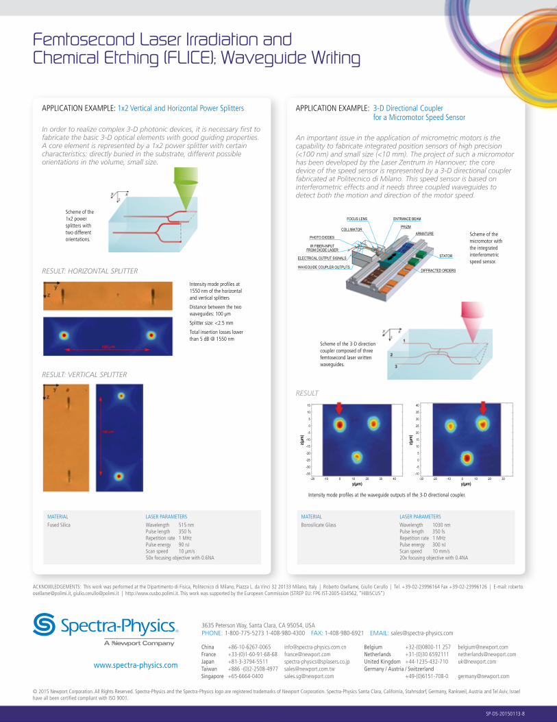
APPLICATION EXAMPLE: 1x2 Vertical and Horizontal Power Splitters APPLICATION EXAMPLE: 3-D Directional Coupler for a Micromotor Speed Sensor
Scheme of the 1x2 power splitters with two different orientations.
Scheme of the micromotor with the integrated interferometric speed sensor.
Intensity mode profiles at 1550 nm of the horizontal and vertical splitters
Distance between the two waveguides: 100 µm
Splitter size: <2.5 mm
Total insertion losses lower than 5 dB @ 1550 nm
Scheme of the 3-D direction coupler composed of three femtosecond laser written waveguides.
In order to realize complex 3-D photonic devices, it is necessary first to fabricate the basic 3-D optical elements with good guiding properties. A core element is represented by a 1x2 power splitter with certain characteristics: directly buried in the substrate, different possible orientations in the volume, small size.
An important issue in the application of micrometric motors is the capability to fabricate integrated position sensors of high precision (<100 nm) and small size (<10 mm). The project of such a micromotor has been developed by the Laser Zentrum in Hannover; the core device of the speed sensor is represented by a 3-D directional coupler fabricated at Politecnico di Milano. This speed sensor is based on interferometric effects and it needs three coupled waveguides to detect both the motion and direction of the motor speed.
RESULT: HORIZONTAL SPLITTER
RESULT: VERTICAL SPLITTER
RESULT
MATERIAL LASER PARAMETERS
Fused Silica Wavelength 515 nm Pulse length 350 fs Repetition rate 1 MHz Pulse energy 90 nJ Scan speed 10 µm/s 50x focusing objective with 0.6NA
MATERIAL LASER PARAMETERS
Borosilicate Glass Wavelength 1030 nm Pulse length 350 fs Repetition rate 1 MHz Pulse energy 300 nJ Scan speed 10 mm/s 20x focusing objective with 0.4NA
y(µm)
z(µm)
15
10
5
0
-5
-10
-15
-20
-25
-30
-35
-20 -10 0 10 20 30 40
y(µm)
z(µm)
40
35
30
25
20
15
10
5
0
-5
-10
-30 -20 -10 0 10 20 30
Intensity mode profiles at the waveguide outputs of the 3-D directional coupler.
ELECTRICAL OUTPUT SIGNALS
IR FIBER-INPUTFROM DIODE LASER
PHOTO DIODES
COLLIMATOR
FOCUS LENS ENTRANCE BEAM
PRIZM
ARMATURE
WAVEGUIDE COUPLER OUTPUTSDIFFRACTED ORDERS
STATOR