
Femtosecond all-optical parallel logic gates based on tunable saturable to reverse saturable...
5
Femtosecond all-optical parallel logic gates based on tunable saturable to reverse saturable absorption in graphene-oxide thin films Sukhdev Roy and Chandresh Yadav Citation: Applied Physics Letters 103, 241113 (2013); doi: 10.1063/1.4846535 View online: http://dx.doi.org/10.1063/1.4846535 View Table of Contents: http://scitation.aip.org/content/aip/journal/apl/103/24?ver=pdfcov Published by the AIP Publishing This article is copyrighted as indicated in the article. Reuse of AIP content is subject to the terms at: http://scitation.aip.org/termsconditions. Downloaded to IP: 134.99.128.41 On: Thu, 26 Dec 2013 15:29:44
Transcript of Femtosecond all-optical parallel logic gates based on tunable saturable to reverse saturable...

Femtosecond all-optical parallel logic gates based on tunable saturable to reversesaturable absorption in graphene-oxide thin filmsSukhdev Roy and Chandresh Yadav Citation: Applied Physics Letters 103, 241113 (2013); doi: 10.1063/1.4846535 View online: http://dx.doi.org/10.1063/1.4846535 View Table of Contents: http://scitation.aip.org/content/aip/journal/apl/103/24?ver=pdfcov Published by the AIP Publishing
This article is copyrighted as indicated in the article. Reuse of AIP content is subject to the terms at: http://scitation.aip.org/termsconditions. Downloaded to IP:
134.99.128.41 On: Thu, 26 Dec 2013 15:29:44
Femtosecond all-optical parallel logic gates based on tunable saturableto reverse saturable absorption in graphene-oxide thin films
Sukhdev Roya) and Chandresh YadavDepartment of Physics and Computer Science, Dayalbagh Educational Institute, Dayalbagh,Agra 282 005, India
(Received 24 September 2013; accepted 17 November 2013; published online 12 December 2013)
A detailed theoretical analysis of ultrafast transition from saturable absorption (SA) to reverse
saturable absorption (RSA) has been presented in graphene-oxide thin films with femtosecond
laser pulses at 800 nm. Increase in pulse intensity leads to switching from SA to RSA with
increased contrast due to two-photon absorption induced excited-state absorption. Theoretical
results are in good agreement with reported experimental results. Interestingly, it is also shown
that increase in concentration results in RSA to SA transition. The switching has been optimized
to design parallel all-optical femtosecond NOT, AND, OR, XOR, and the universal NAND and
NOR logic gates. VC 2013 AIP Publishing LLC. [http://dx.doi.org/10.1063/1.4846535]
The design of all-optical ultrafast devices is a major
challenge to achieve the next generation ultrahigh bandwidth
information processing. This requires a nonlinear optical
(NLO) material that exhibits fast response, strong nonlinear-
ity, broad wavelength range, low optical loss, high damage
threshold, low-power consumption, low cost, and ease of
integration into optical systems.1
Graphene oxide has emerged as an attractive photonic
material due to its unique properties.2 It exhibits (i) heteroge-
neous chemical and electronic structures, (ii) can be proc-
essed in solution, (iii) interacts with a wide range of organic
and inorganic materials that facilitates synthesis of functional
hybrids and composites with unusual properties, and (iv) its
band gap can be tuned by controlling the sp2 and sp3 fractions
to tailor its electrical, optical, and chemical properties.2
A wide range of applications has been proposed for
graphene-oxide (GO) and reduced graphene oxide (rGO).2–6
Its high transparency in the visible spectrum has been inves-
tigated for transparent conductor applications as a possible
replacement for indium-tin oxide (ITO) in organic solar
cells, organic light-emitting devices (LEDs), and displays.2
Its intrinsic tunable fluorescence in the visible and near infra-
red (NIR) has led to biological applications for bio-imaging,
sensing, and drug delivery.2 GO films with very high dielec-
tric constant have been used as spacers to realize thin film
super capacitors.3 rGO obtained from chemical vapor depo-
sition or thermal reduction of GO has been used as one elec-
trode in diode-based memories, solar cells, and LEDs.4 The
strong modulation conductance by strain has been used to
fabricate rGO channel field-effect transistors for ultrasensi-
tive strain sensing.5 The strong saturable absorption (SA) of
GO has also been used for Q-switching and femtosecond (fs)
mode-locking of erbium-doped ring-cavity fiber lasers.6
The NLO properties of GO have been experimentally
investigated in the nanosecond (ns), picosecond (ps), and fs
regimes at different wavelengths, primarily for broadband
optical limiting.2,7–9 These studies show that the NLO prop-
erties of GO are determined by the combined action of the
sp2 and sp3 domains. For ns and ps pulse excitation at
532 nm and also for fs pulse excitation at 800 nm in GO dis-
persed in different solvents and thin films, a transition from
SA to reverse saturable absorption (RSA) takes place on
increase in intensity with increased contrast.7–9 The charge
carriers with SA from the sp2–hybridized domains dominate
the NLO response at low pump intensities while the influ-
ence of the two-photon absorption (TPA) from the sp3–
hybridized domains on the transient absorption signal
becomes stronger on increase in pump intensity.
Logic gates based on switches are the basic building
blocks of computing circuits. In a variety of materials, the
SA characteristics have been used to design all-optical OR
and AND logic gates whereas RSA characteristics have been
used for NOT and the universal NAND and NOR logic gates,
in a pump-probe setup.10,11 These designs require different
samples that exhibit either SA or RSA based on the lower or
higher lifetime of the excited-states, respectively. However,
the intensity-dependent ultrafast SA to RSA transition can be
advantageous in simultaneous realization of various all-
optical ultrafast logic gates with the same sample.
In this letter, we theoretically analyze ultrafast transitions
in GO thin films to study the effect of excitation intensity,
pulse width, concentration, two-photon and three-photon
absorption (3PA) coefficients, and pulse frequency on the SA
to RSA switching and optimize it to design all-optical ultra-
fast parallel OR, AND, XOR, NOT, and the universal NAND
and NOR logic gates.
We consider the four-level energy diagram to analyze
the fs nonlinear absorption (NLA) dynamics in GO thin films
as shown in the inset of Fig. 1. Ultrafast transitions in GO
involve only the singlet states (S0! Sn). One-photon absorp-
tion (S0! S1) and TPA (S0! S2) are as shown in the figure.
TPA from S1 to Sn is not allowed as it occurs between states
of even parities. Electrons in S2 absorb another photon to
reach Sn through excited-state absorption (ESA) as TPA from
S0 to S2 is predominant. TPA and ESA contribute to the vari-
ation in intensity with absorption coefficients b and c, which
correspond to the third and fifth-order nonlinear coefficients,
respectively. The rate of change of the population densities ina)E-mail: [email protected].
0003-6951/2013/103(24)/241113/4/$30.00 VC 2013 AIP Publishing LLC103, 241113-1
APPLIED PHYSICS LETTERS 103, 241113 (2013)
This article is copyrighted as indicated in the article. Reuse of AIP content is subject to the terms at: http://scitation.aip.org/termsconditions. Downloaded to IP:
134.99.128.41 On: Thu, 26 Dec 2013 15:29:44

different energy states can be described by the following
equations:
dN0
dt¼ � r0IN0
�hxþ N1
s1
� bI2
2�hx; (1)
dN1
dt¼ r0IN0
�hx� r1IN1
�hx� N1
s1
þ N2
s2
; (2)
dN2
dt¼ r1IN1
�hx� r2IN2
�hx� N2
s2
þ N3
s3
þ bI2
2�hx; (3)
dN3
dt¼ r2IN2
�hx� N3
s3
; (4)
where N0, N1, N2, N3 are the population densities of S0, S1,
S2, and Sn states, respectively, r0, r1, and r2 are the absorp-
tion cross-sections of S0! S1, S1! S2, and S2! Sn transi-
tions, respectively, and s1, s2, and s3 are the corresponding
life times. The transmitted intensity through the film can be
written as
dI
dz¼ �aI ¼ �½aef f þ bI þ cI2�I; (5)
where aeff¼ a0/(1þ I/Is) with a0 as the linear absorption
coefficient and Is as the saturation intensity. The Gaussian
modulating excitation laser pulse is given by
I ¼ I0
x20
x2ðzÞ exp �ct2
s2p
! !exp � 2r2
x2ðzÞ
!; (6)
where x(z)¼x0{1þ (z/z0)2}1/2, c¼ 4ln2 as the pulse profile
parameter, I0 as the peak pulse intensity, and z0¼ px02/k,
with x0 as the radius of the beam waist.
To analyze two input logic gates configurations, we con-
sider two single laser pulses such that the four input combi-
nations (0,0), (0,1), (1,0), and (1,1) can be considered in
terms of phase differences of their peaks.11,12
NLA characteristics have been computed using Eqs.
(1)–(6) considering the experimental parameters for GO thin
films.9,13,14 We consider a laser pulse from a Ti:sapphire
regeneration amplifier at 800 nm of pulse width sp¼ 100 fs
to excite the film. The experimental values of various param-
eters used in the computation are r0¼ 5.5� 10�19 cm2,
r1¼ 1.5� 10�17 cm2, r2¼ 7.4� 10�19 cm2, s1¼ 66 ps,
s2¼ 4.3 ps, s3¼ 0.37 ps, Is¼ 7.0� 1010 W/cm2, concentra-
tion 25 mM, film thickness 140 nm, and wo¼ 20 lm.9,13,14
The contributions of ESA and multi-photon absorption are
difficult to distinguish using z-scan experimental technique;
hence, the reported fitting experimental results which give
effective TPA (beff¼ 31� 10�9 cm/W) and 3PA coefficients
(ceff¼ 0.47� 10�18 cm3/W2) have been used for computation.9
The variation of normalized transmitted intensity with
time at different peak input pulse intensities is shown in
Fig. 1. At I0¼ 5.0� 1010 W/cm2, SA is observed as mole-
cules get excited from S0 to populate S1 and S2 states,
which increases on increase in I0 to 11� 1010 W/cm2. At
I0¼ 11.3� 1010 W/cm2, there is a transition from SA to
RSA due to TPA-induced ESA. Further increase in I0
results in increased contrast due to increase in ESA. This is
evident from the corresponding variation in normalized
population density with time at different I0 values as shown
in Fig. 2. Continuous increase in N2 and N1 leads to
increased ESA from S2 to Sn so that the normalized trans-
mitted intensity exhibits a dip with increasing contrast. At
I0¼ 55� 1010 W/cm2, 68% modulation can be achieved
with switch off/on time of 80 fs. Theoretical simulations
are in good agreement with experimental results shown
recently.9
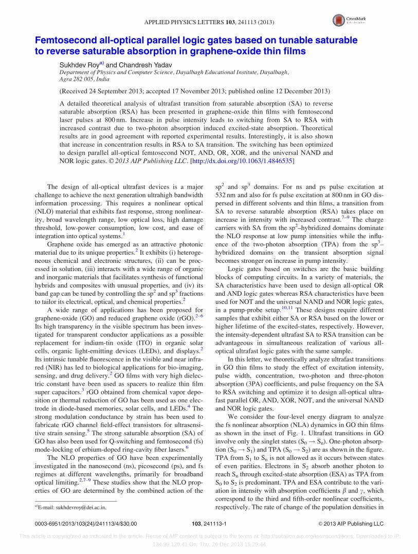
NLO response is sensitive to concentration. Interestingly,
the variation of transmittance with time for different concen-
tration values exhibits a reverse behavior with regards to peak
pump intensity. In this case, the transition from RSA to SA
takes place at 11.8 mM on increase in concentration as shown
in Fig. 3. The population of N2 reduces with increase in con-
centration. The variation indicates that concentration affects
TPA-induced ESA that is greater at lower concentration. It
has been shown in 4-methoxy-2-nitroaniline that both effec-
tive TPA and ESA cross-sections decrease with increase in
concentration and the effective lifetimes of TPA-induced
ESA increases.15 The variation of percentage modulation with
concentration at different I0 values is also shown in Fig. 4. It
FIG. 1. Variation of transmittance with time during a single 100 fs laser
pulse for different I0 values. Inset shows the four-level energy diagram to
describe NLA in the fs regime.
FIG. 2. Variation of normalized population density with time for different I0
values (a) and (b).
241113-2 S. Roy and C. Yadav Appl. Phys. Lett. 103, 241113 (2013)
This article is copyrighted as indicated in the article. Reuse of AIP content is subject to the terms at: http://scitation.aip.org/termsconditions. Downloaded to IP:
134.99.128.41 On: Thu, 26 Dec 2013 15:29:44
is evident that the RSA-SA transition occurs at higher concen-
tration for higher values of I0. At higher values of I0, beff, and
ceff contributions become significant. The SA to RSA transi-
tion intensity (TI) value is sensitive to beff and ceff. The de-
pendence is shown in inset of Fig. 4. There is a monotonic
decrease in the transition intensity on increase in the value of
the TPA and 3PA coefficients, respectively.
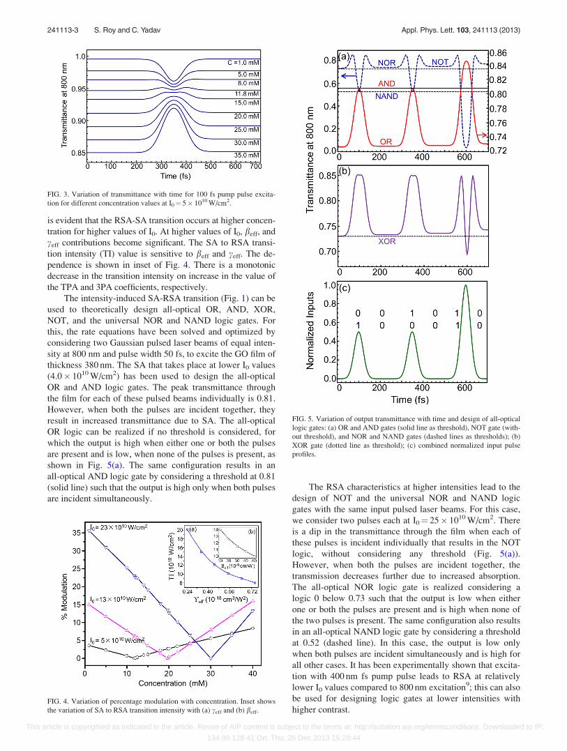
The intensity-induced SA-RSA transition (Fig. 1) can be
used to theoretically design all-optical OR, AND, XOR,
NOT, and the universal NOR and NAND logic gates. For
this, the rate equations have been solved and optimized by
considering two Gaussian pulsed laser beams of equal inten-
sity at 800 nm and pulse width 50 fs, to excite the GO film of
thickness 380 nm. The SA that takes place at lower I0 values
(4.0� 1010 W/cm2) has been used to design the all-optical
OR and AND logic gates. The peak transmittance through
the film for each of these pulsed beams individually is 0.81.
However, when both the pulses are incident together, they
result in increased transmittance due to SA. The all-optical
OR logic can be realized if no threshold is considered, for
which the output is high when either one or both the pulses
are present and is low, when none of the pulses is present, as
shown in Fig. 5(a). The same configuration results in an
all-optical AND logic gate by considering a threshold at 0.81
(solid line) such that the output is high only when both pulses
are incident simultaneously.
The RSA characteristics at higher intensities lead to the
design of NOT and the universal NOR and NAND logic
gates with the same input pulsed laser beams. For this case,
we consider two pulses each at I0¼ 25� 1010 W/cm2. There
is a dip in the transmittance through the film when each of
these pulses is incident individually that results in the NOT
logic, without considering any threshold (Fig. 5(a)).
However, when both the pulses are incident together, the
transmission decreases further due to increased absorption.
The all-optical NOR logic gate is realized considering a
logic 0 below 0.73 such that the output is low when either
one or both the pulses are present and is high when none of
the two pulses is present. The same configuration also results
in an all-optical NAND logic gate by considering a threshold
at 0.52 (dashed line). In this case, the output is low only
when both pulses are incident simultaneously and is high for
all other cases. It has been experimentally shown that excita-
tion with 400 nm fs pump pulse leads to RSA at relatively
lower I0 values compared to 800 nm excitation9; this can also
be used for designing logic gates at lower intensities with
higher contrast.
FIG. 3. Variation of transmittance with time for 100 fs pump pulse excita-
tion for different concentration values at I0¼ 5� 1010 W/cm2.
FIG. 4. Variation of percentage modulation with concentration. Inset shows
the variation of SA to RSA transition intensity with (a) ceff and (b) beff.
FIG. 5. Variation of output transmittance with time and design of all-optical
logic gates: (a) OR and AND gates (solid line as threshold), NOT gate (with-
out threshold), and NOR and NAND gates (dashed lines as thresholds); (b)
XOR gate (dotted line as threshold); (c) combined normalized input pulse
profiles.
241113-3 S. Roy and C. Yadav Appl. Phys. Lett. 103, 241113 (2013)
This article is copyrighted as indicated in the article. Reuse of AIP content is subject to the terms at: http://scitation.aip.org/termsconditions. Downloaded to IP:
134.99.128.41 On: Thu, 26 Dec 2013 15:29:44
The all-optical XOR logic gate can be realized by oper-
ating near the SA-RSA transition (Fig. 5(b)). For this case,
we consider two pulses each of I0¼ 9.7� 1010 W/cm2 and a
threshold at 0.73. Now, the output is high for each of
these pulses incident individually. However, when both the
pulses are incident together, RSA results in greater absorp-
tion that leads to a strong dip in the output to result in a 0
logic state. Hence, the intensity-induced ultrafast SA-RSA
transition in GO thin film can effectively be used to realize
various multiple input Boolean logic operations in the fs
domain, with the same setup by only controlling the excita-
tion intensity.
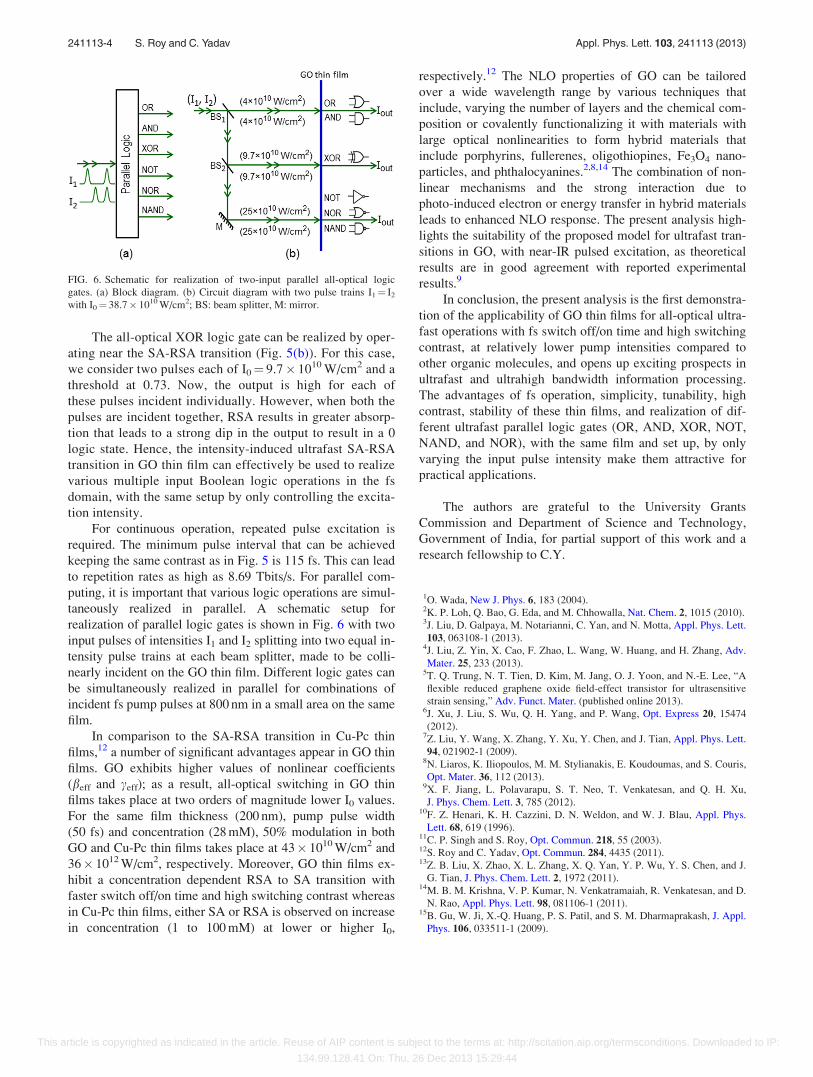
For continuous operation, repeated pulse excitation is
required. The minimum pulse interval that can be achieved
keeping the same contrast as in Fig. 5 is 115 fs. This can lead
to repetition rates as high as 8.69 Tbits/s. For parallel com-
puting, it is important that various logic operations are simul-
taneously realized in parallel. A schematic setup for
realization of parallel logic gates is shown in Fig. 6 with two
input pulses of intensities I1 and I2 splitting into two equal in-
tensity pulse trains at each beam splitter, made to be colli-
nearly incident on the GO thin film. Different logic gates can
be simultaneously realized in parallel for combinations of
incident fs pump pulses at 800 nm in a small area on the same
film.
In comparison to the SA-RSA transition in Cu-Pc thin
films,12 a number of significant advantages appear in GO thin
films. GO exhibits higher values of nonlinear coefficients
(beff and ceff); as a result, all-optical switching in GO thin
films takes place at two orders of magnitude lower I0 values.
For the same film thickness (200 nm), pump pulse width
(50 fs) and concentration (28 mM), 50% modulation in both
GO and Cu-Pc thin films takes place at 43� 1010 W/cm2 and
36� 1012 W/cm2, respectively. Moreover, GO thin films ex-
hibit a concentration dependent RSA to SA transition with
faster switch off/on time and high switching contrast whereas
in Cu-Pc thin films, either SA or RSA is observed on increase
in concentration (1 to 100 mM) at lower or higher I0,
respectively.12 The NLO properties of GO can be tailored
over a wide wavelength range by various techniques that
include, varying the number of layers and the chemical com-
position or covalently functionalizing it with materials with
large optical nonlinearities to form hybrid materials that
include porphyrins, fullerenes, oligothiopines, Fe3O4 nano-
particles, and phthalocyanines.2,8,14 The combination of non-
linear mechanisms and the strong interaction due to
photo-induced electron or energy transfer in hybrid materials
leads to enhanced NLO response. The present analysis high-
lights the suitability of the proposed model for ultrafast tran-
sitions in GO, with near-IR pulsed excitation, as theoretical
results are in good agreement with reported experimental
results.9
In conclusion, the present analysis is the first demonstra-
tion of the applicability of GO thin films for all-optical ultra-
fast operations with fs switch off/on time and high switching
contrast, at relatively lower pump intensities compared to
other organic molecules, and opens up exciting prospects in
ultrafast and ultrahigh bandwidth information processing.
The advantages of fs operation, simplicity, tunability, high
contrast, stability of these thin films, and realization of dif-
ferent ultrafast parallel logic gates (OR, AND, XOR, NOT,
NAND, and NOR), with the same film and set up, by only
varying the input pulse intensity make them attractive for
practical applications.
The authors are grateful to the University Grants
Commission and Department of Science and Technology,
Government of India, for partial support of this work and a
research fellowship to C.Y.
1O. Wada, New J. Phys. 6, 183 (2004).2K. P. Loh, Q. Bao, G. Eda, and M. Chhowalla, Nat. Chem. 2, 1015 (2010).3J. Liu, D. Galpaya, M. Notarianni, C. Yan, and N. Motta, Appl. Phys. Lett.
103, 063108-1 (2013).4J. Liu, Z. Yin, X. Cao, F. Zhao, L. Wang, W. Huang, and H. Zhang, Adv.
Mater. 25, 233 (2013).5T. Q. Trung, N. T. Tien, D. Kim, M. Jang, O. J. Yoon, and N.-E. Lee, “A
flexible reduced graphene oxide field-effect transistor for ultrasensitive
strain sensing,” Adv. Funct. Mater. (published online 2013).6J. Xu, J. Liu, S. Wu, Q. H. Yang, and P. Wang, Opt. Express 20, 15474
(2012).7Z. Liu, Y. Wang, X. Zhang, Y. Xu, Y. Chen, and J. Tian, Appl. Phys. Lett.
94, 021902-1 (2009).8N. Liaros, K. Iliopoulos, M. M. Stylianakis, E. Koudoumas, and S. Couris,
Opt. Mater. 36, 112 (2013).9X. F. Jiang, L. Polavarapu, S. T. Neo, T. Venkatesan, and Q. H. Xu,
J. Phys. Chem. Lett. 3, 785 (2012).10F. Z. Henari, K. H. Cazzini, D. N. Weldon, and W. J. Blau, Appl. Phys.
Lett. 68, 619 (1996).11C. P. Singh and S. Roy, Opt. Commun. 218, 55 (2003).12S. Roy and C. Yadav, Opt. Commun. 284, 4435 (2011).13Z. B. Liu, X. Zhao, X. L. Zhang, X. Q. Yan, Y. P. Wu, Y. S. Chen, and J.
G. Tian, J. Phys. Chem. Lett. 2, 1972 (2011).14M. B. M. Krishna, V. P. Kumar, N. Venkatramaiah, R. Venkatesan, and D.
N. Rao, Appl. Phys. Lett. 98, 081106-1 (2011).15B. Gu, W. Ji, X.-Q. Huang, P. S. Patil, and S. M. Dharmaprakash, J. Appl.
Phys. 106, 033511-1 (2009).
FIG. 6. Schematic for realization of two-input parallel all-optical logic
gates. (a) Block diagram. (b) Circuit diagram with two pulse trains I1¼ I2
with I0¼ 38.7� 1010 W/cm2; BS: beam splitter, M: mirror.
241113-4 S. Roy and C. Yadav Appl. Phys. Lett. 103, 241113 (2013)
This article is copyrighted as indicated in the article. Reuse of AIP content is subject to the terms at: http://scitation.aip.org/termsconditions. Downloaded to IP:
134.99.128.41 On: Thu, 26 Dec 2013 15:29:44


![Hybrid femtosecond laser fabrication of a size-tunable microtrap …mane.ustc.edu.cn/uploadfile/2020/0218/20200218125235974.pdf · 2020. 2. 18. · hydrodynamic trap arrays [15,16]](https://static.fdocuments.in/doc/165x107/611d3122a2e0675a58304809/hybrid-femtosecond-laser-fabrication-of-a-size-tunable-microtrap-maneustceducnuploadfile20200218.jpg)


