FEDL7029-04 ML7029 - lapis-semi.com fileFEDL7029-04 ML7029 2/29 BLOCK DIAGRAM LPF PCM Expander A/D...
29
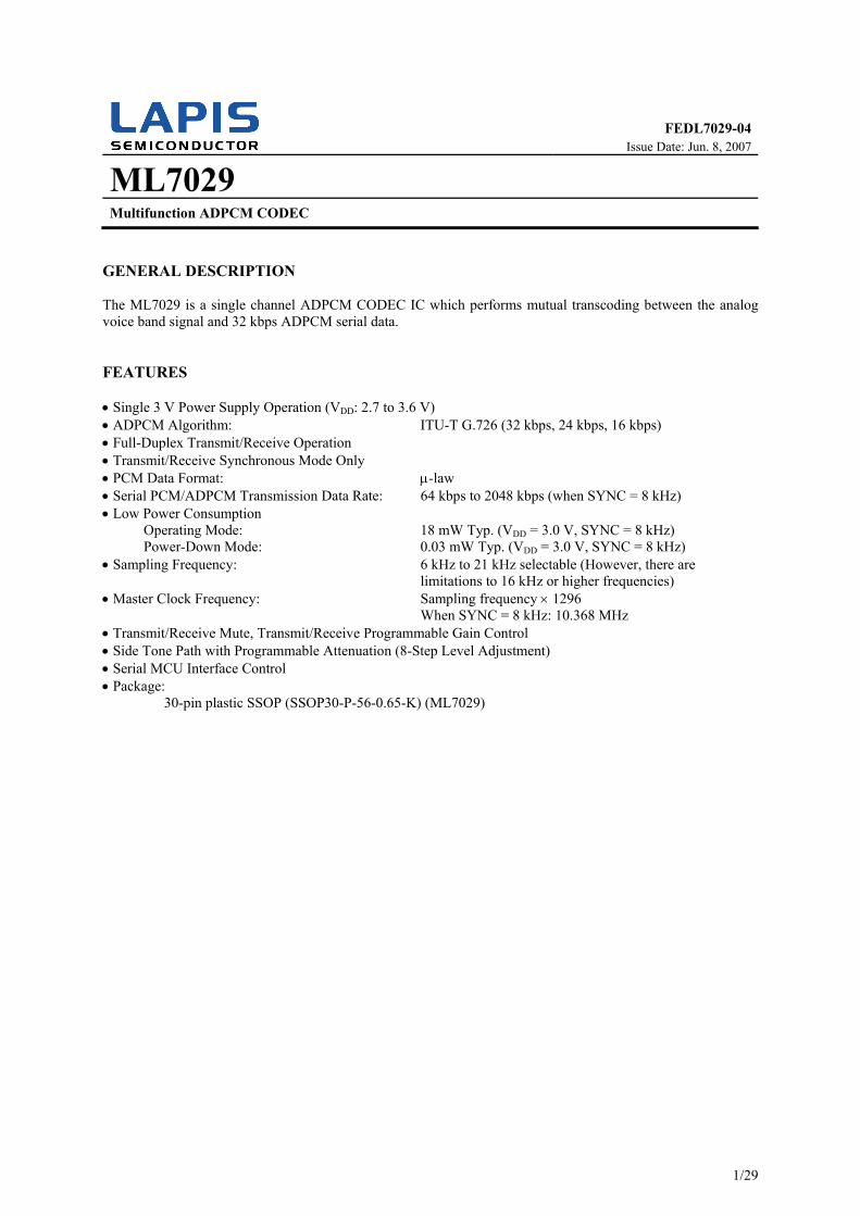
FEDL7029-04 Issue Date: Jun. 8, 2007 ML7029 Multifunction ADPCM CODEC 1/29 GENERAL DESCRIPTION The ML7029 is a single channel ADPCM CODEC IC which performs mutual transcoding between the analog voice band signal and 32 kbps ADPCM serial data. FEATURES Single 3 V Power Supply Operation (V DD : 2.7 to 3.6 V) ADPCM Algorithm: ITU-T G.726 (32 kbps, 24 kbps, 16 kbps) Full-Duplex Transmit/Receive Operation Transmit/Receive Synchronous Mode Only PCM Data Format: -law Serial PCM/ADPCM Transmission Data Rate: 64 kbps to 2048 kbps (when SYNC = 8 kHz) Low Power Consumption Operating Mode: 18 mW Typ. (V DD = 3.0 V, SYNC = 8 kHz) Power-Down Mode: 0.03 mW Typ. (V DD = 3.0 V, SYNC = 8 kHz) Sampling Frequency: 6 kHz to 21 kHz selectable (However, there are limitations to 16 kHz or higher frequencies) Master Clock Frequency: Sampling frequency 1296 When SYNC = 8 kHz: 10.368 MHz Transmit/Receive Mute, Transmit/Receive Programmable Gain Control Side Tone Path with Programmable Attenuation (8-Step Level Adjustment) Serial MCU Interface Control Package: 30-pin plastic SSOP (SSOP30-P-56-0.65-K) (ML7029)
Transcript of FEDL7029-04 ML7029 - lapis-semi.com fileFEDL7029-04 ML7029 2/29 BLOCK DIAGRAM LPF PCM Expander A/D...
FEDL7029-04Issue Date: Jun. 8, 2007
ML7029 Multifunction ADPCM CODEC
1/29
GENERAL DESCRIPTION The ML7029 is a single channel ADPCM CODEC IC which performs mutual transcoding between the analog voice band signal and 32 kbps ADPCM serial data. FEATURES Single 3 V Power Supply Operation (VDD: 2.7 to 3.6 V) ADPCM Algorithm: ITU-T G.726 (32 kbps, 24 kbps, 16 kbps) Full-Duplex Transmit/Receive Operation Transmit/Receive Synchronous Mode Only PCM Data Format: -law Serial PCM/ADPCM Transmission Data Rate: 64 kbps to 2048 kbps (when SYNC = 8 kHz) Low Power Consumption Operating Mode: 18 mW Typ. (VDD = 3.0 V, SYNC = 8 kHz) Power-Down Mode: 0.03 mW Typ. (VDD = 3.0 V, SYNC = 8 kHz) Sampling Frequency: 6 kHz to 21 kHz selectable (However, there are
limitations to 16 kHz or higher frequencies) Master Clock Frequency: Sampling frequency 1296 When SYNC = 8 kHz: 10.368 MHz Transmit/Receive Mute, Transmit/Receive Programmable Gain Control Side Tone Path with Programmable Attenuation (8-Step Level Adjustment) Serial MCU Interface Control Package:
30-pin plastic SSOP (SSOP30-P-56-0.65-K) (ML7029)

FEDL7029-04
ML7029
2/29
BLOCK DIAGRAM
LPFPCM
Expander
A/D Conv.
BPF/LPF
PCM Compander PCMSO
PCMRI
AIN–
GSX
D/A Conv.
VFRO
VREF SG
MCU I/F
VA
VD
DG
AG
MC
K
PD
N
DO
UT
DIN
DE
N
EX
CK
BCLK
SYNC
20 k
20 k
CR2-B6 to B4
CR2-B2 to B0
CR3-B7 to B5ADPCM
PCMSI
IS
IR
PCMRO
CR2-B7
TXON/
OFF
CR2-B3
RXON/
OFF

FEDL7029-04
ML7029
3/29
PIN CONFIGURATION (TOP VIEW)
1
2
3
4
5
6
7
8
9
10
11
12
13
14
15
30
29
28
27
26
25
24
23
22
21
20
19
18
17
16
GSX
AIN–
SG
VA
AG
VFRO
DG PDN
VD BCLK SYNC PCMSO PCMSI IS IR PCMRO PCMRI MCK DEN EXCK DIN DOUT
NC
NC
NC
NC
NC
NC NC
NC
NC: No Connection
30-Pin Plastic SSOP

FEDL7029-04
ML7029
4/29
PIN FUNCTIONAL DESCRIPTIONS AIN–, GEX Transmit analog input and transmit level adjustment. AIN– is connected to the inverting input of the transmit amplifier. GSX is connected to the transmit amplifier output. During power-down mode, the GSX output is a high impedance state. VFRO Receive analog output. During power-down mode, the VFRO output is in a high impedance state. SG Analog signal ground. The output voltage of this pin is approximately 1.4 V. Put 10 F plus 0.1 F (ceramic type) bypass capacitors between this pin and AG. During power-down, this output voltage is 0 V. This pin should be used via a buffer if used externally. AG Analog ground. DG Digital ground. This ground is separated from the analog signal ground pin (AG). The DG pin must be kept as close as possible to AG on the PCB. Va Analog +3 V power supply. VD Digital +3 V power supply. This power supply is separated from the analog signal power supply pin (VA). The VD pin must be kept as close as possible to VA on the PCB. PDN Power-down and reset control input. A “0” level makes the IC enter a power-down state. At the same time, all control register data are reset to the initial state. Set this pin to “1” during normal operating mode. The power-down state is controlled by a logical OR with CR0-B5 of the control register. When using PDN for power-down and reset control, set CR0-B5 to digital “0”. The reset width (a “L” level period) should be 200 ns or more. Be sure to reset the control registers by executing this power down to keep this pin to digital “0”level for 200 ns or longer after the power is turned on and VDD exceeds 2.7 V.

FEDL7029-04
ML7029
5/29
MCK Master clock input. The frequency is 1296 times the SYNC signal. For example, it is 10.368 MHz when the SYNC signal is 8 kHz. The master clock signal may be asynchronous with BCLK and SYNC. PCMSO Transmit PCM data output. PCM is output from MSB in synchronization with the rising edge of BCLK and XSYNC. Refer to Figure 1. During power-down, the PCMSO output is at “L” level. PCMSI Transmit PCM data input. This signal is converted to the transmit ADPCM data, PCM is shifted in synchronization with the falling edge of BCLK. Normally, this pin is connected to PCMSO. Refer to Figure 1. PCMRO Receive PCM data output. PCM is the output signal after ADPCM decoder processing. This signal is output serially from MSB in synchronization with the rising edge of BCLK and RSYNC. Refer to Figure 1. During power-down, the PCMRO output is at “L” level. PCMRI Receive PCM data input. PCM is shifted on the rising edge of the BCLK and input from MSB. Normally, this pin is connected to PCMRO. Refer to Figure 1. IS Transmit ADPCM signal output. After having encoded PCM with ADPCM, the signal is output from MSB in synchronization with the rising edge of BCLK and XSYNC. Refer to Figure 1. This pin is at “H” level during power-down. IR Receive ADPCM signal input. This input signal is shifted serially on the falling edge of BCLK and SYNC and input from MSB. Refer to Figure 1. BCLK Shift clock input for the PCM and ADPCM data. The frequency is set in the range of 8 to 256 times the SYNC frequency. Refer to Figure 1.

FEDL7029-04
ML7029
6/29
SYMC Sampling input for the PCM and ADPCM data. The frequency is 8 kHz or 11.025 kHz and is selected by the control register data CR3-B1. Synchronize this signal with BCLK signal. SYNC is used to indicate the MSB of the PCM data stream. Refer to Figure 1.
Figure 1 PCM and ADPCM Interface Basic Timing
125 s (SYNC = 8 kHz)
BCLK
SYNC
MSB LSB PCMSO/PCMSI/PCMRO/PCMRI
MSB LSBIS/IR
FEDL7029-04
ML7029
7/29
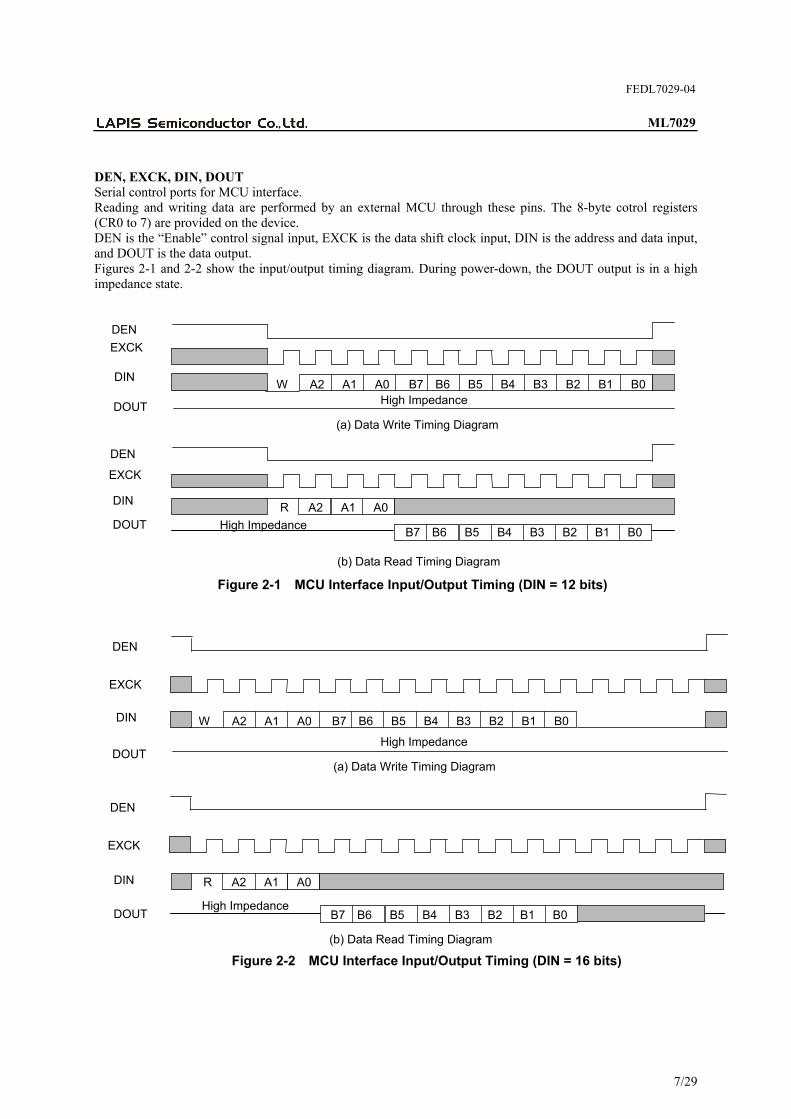
DEN, EXCK, DIN, DOUT Serial control ports for MCU interface. Reading and writing data are performed by an external MCU through these pins. The 8-byte cotrol registers (CR0 to 7) are provided on the device. DEN is the “Enable” control signal input, EXCK is the data shift clock input, DIN is the address and data input, and DOUT is the data output. Figures 2-1 and 2-2 show the input/output timing diagram. During power-down, the DOUT output is in a high impedance state.
Figure 2-1 MCU Interface Input/Output Timing (DIN = 12 bits)
(a) Data Write Timing Diagram
(b) Data Read Timing Diagram
EXCK
A2 A1 A0W B7 B6 B5 B4 B3 B2 B1 B0
DEN
DIN
DOUT High Impedance
EXCK
DEN
A2 A1 A0R DIN
B7 B6 B5 B4 B3 B2 B1 B0 DOUT High Impedance
EXCK
DEN
DIN
EXCK
DEN
DIN
Figure 2-2 MCU Interface Input/Output Timing (DIN = 16 bits)
DOUT
DOUT
B7 B6 B5 B4 B3 B2 B1 B0
(a) Data Write Timing Diagram
High Impedance
A2 A1 A0 W
(b) Data Read Timing Diagram
A2 A1 A0 R
B7 B6 B5 B4 B3 B2 B1 B0 High Impedance

FEDL7029-04
ML7029
8/29
Table 1 shows the register map.
Table 1 Control Register Map
Address Control and Detect Data Name
A2 A1 A0 B7 B6 B5 B4 B3 B2 B1 B0 R/W
CR0 0 0 0 — — PDN
ALL — — — — — R/W
CR1 0 0 1 MODE 1 MODE 0 TX
RESETRX
RESETTX
MUTERX
MUTE—
RX
PAD R/W
CR2 0 1 0 TX
ON/OFF
TX
GAIN2
TX
GAIN1
TX
GAIN0
RX
ON/OFF
RX
GAIN2
RX
GAIN1
RX
GAIN0 R/W
CR3 0 1 1 Side Tone
GAIN2
Side Tone
GAIN1
Side Tone
GAIN0— — —
HPF
8k/11k
HPF
ON/OFF R/W
R/W : Read/Write enable

FEDL7029-04
ML7029
9/29
ABSOLUTE MAXIMUM RATINGS
Parameter Symbol Condition Rating Unit
Power Supply Voltage VDD — –.3 to +5.0 V
Analog Input Voltage VAIN — –0.3 to VDD+0.3 V
Digital Input Voltage VDIN — –0.3 to VDD+0.3 V
Storage Temperature Tstg — –55 to +150 C
RECOMMENDED OPERATION CONDITIONS Parameter Symbol Condition Min. Typ. Max. Unit
Power Supply Voltage VDD Voltage must be fixed +2.7 3.0 +3.6 V
Operating Temperature Range
Ta — –25 +25 +70 C
Digital Input High Voltage VIH Digital Input Pins 0.45 VDD — VDD V
Digital Input Low Voltage VIL Digital Input Pins 0 — 0.16 VDD V
Master Clock Frequency fMCK1 MCK 7.776 10.368 20.736 MHz
Master Clock Frequency Accuracy
fMCK2 MCK –0.01%SYNC
1296 +0.01% MHz
Bit Clock Duty fBCK BCLK SYNC 8 — SYNC
256 kHz
Sampling Frequency (*1) fSYNC SYNC 6.0 8.0 16 kHz
Master Clock Duty Ratio DMCK MCK(20.736 MHz) 30 50 70 %
Clock Duty Ratio DCLK BCLK, EXCK 30 50 70 %
Digital Input Rise Time tir Digital Input Pins — — 50 ns
Digital Input Fall Time tif Digital Input Pins — — 50 ns
PCM Sync Signal Setting Time (Continuous BCLK)
tBS BCLKSYNC (see Fig. 3-1)
100 — — ns
PCM Sync Signal Setting Time (Burst Mode Clock)
tSB BCLK SYNC (see Fig. 3-2)
0 — 20 s
SYNC Signal Width (Continuous BCLK)
tWS SYNC (see Fig. 3-1) 1BCLK — SYNC –1
BCLK s
SYNC Signal Width (Burst Mode Clock)
tWSB SYNC (see Fig. 3-2) 1BCLK — Burst
Clock –1 s
PCM, ADPCM Setup Time tDS — 100 — — ns
PCM, ADPCM Hold Time tDH — 100 — — ns
Digital Output Load CDL Digital Output Pins — — 100 pF
Bypass Capacitors for SG CSG SG to AG 10+0.1 — — F
*1: Refer to the Appendix.
FEDL7029-04
ML7029
10/29
ELECTRICAL CHARACTERISTICS DC Characteristics
(VDD = 2.7 to 3.6 V, Ta = –25 to +70C)
Parameter Symbol Condition Min. Typ. Max. Unit
Power Supply Current IDD1 Operating Mode No Signal — 6.0 12 mA
(VDD = 3.0 V, SYNC = 8 kHz) IDD2 Power Down Mode
(Input pins are fixed) — 0.01 0.1 mA
Input Leakage Current IIH VI = VDD — — 2.0 µA
IIL VI = 0 V — — 0.5 µA
Output High Voltage VOH IOH = 4 mA 2.4 — — V
Output Low Voltage VOL IOL = –4 mA — — 0.4 V
Input Capacitance CIN — — 5 — pF
Analog Interface Characteristics
(VDD= 2.7 to 3.6 V, Ta = –25 to +70C)
Parameter Symbol Condition Min. Typ. Max. Unit
Input Resistance RIN AIN– — 10 — M
Output Load Resistance RL GSX, VFRO 20 — — k
Output Load Capacitance CL GSX, VFRO — — 100 pF
Output Amplitude (*2) VO1 GSX, VFRO (RL = 20 k) — — 1.3 VPP
Offset Voltage VOF GSX, VFRO –100 — +100 mV
SG Output Voltage VSG SG — 1.4 — V
SG Output Resistance RSG SG — 40 — k
SG Warm-up Time TSG SGAG 10+0.1F
(Rise time to max. 90% level)— 700 — ms
*2: –7.7 dBm (600) = 0 dBm0, +3.17 dBm0 = 1.3 VPP
FEDL7029-04
ML7029
11/29
AC Characteristics (VDD = 2.7 to 3.6 V, Ta = –25 to +70C)
Condition Parameter Symbol
Freg. (Hz) Level (dBm0)Min. Typ. Max. Unit
LB8T1 60 30 — — dB LB8T2 300 –0.5 — 1.5 dB LB8T3 1015 Reference dB LB8T4 3400 –0.5 — 1.0 dB
Transmit Frequency Response SYNC = 8 kHz BPF
LB8T5 3970
0
12 — — dB LB11T1 60 30 — — dB LB11T2 300 –0.5 — 1.5 dB LB11T3 1400 Reference dB LB11T4 4690 –0.5 — 1.0 dB
Transmit Frequency Response SYNC = 11.025 kHz BPF
LB11T5 5470
0
12 — — dB LL8T1 300 –0.5 — 0.5 dB LL8T2 1015 Reference dB LL8T3 3400 –0.5 — 1.0 dB
Transmit Frequency Response SYNC = 8 kHz LPF LL8T4 3970
0
12 — — dB LL11T1 300 –0.5 — 0.5 dB LL11T2 1400 Reference dB LL11T3 4690 –0.5 — 1.0 dB
Transmit Frequency Response SYNC = 11.025 kHz LPF LL11T4 5470
0
12 — — dB LL8R1 300 –0.5 — 0.5 dB LL8R2 1015 Reference dB LL8R3 3400 –0.5 — 1.0 dB
Receive Frequency Response SYNC = 8 kHz LPF LL8R4 3970
0
12 — — dB LL11R1 300 –0.5 — 0.5 dB LL11R2 1400 Reference dB LL11R3 4690 –0.5 — 1.0 dB
Receive Frequency Response SYNC = 11.025 kHz LPF LL11R4 5470
0
12 — — dB SD8T1 3 35 — — dB Transmit S/N Ratio
SYNC = 8 kHz (*3) SD8T2 f = 1015 Hz
–40 28 — — dB SD8R1 3 35 — — dB Receive S/N Ratio
SYNC = 8 kHz (*3) SD8R2 f = 1015 Hz
–40 28 — — dB SD16T1 3 35 — — dB Transmit S/N Ratio
SYNC = 16 kHz (*3) SD16T2 f = 1015 Hz
–40 28 — — dB SD16R1 3 35 — — dB Receive S/N Ratio
SYNC = 16 kHz (*3) SD16R2 f = 1015 Hz
–40 28 — — dB
NIDLT AIN– = SG — — –68 dBm0pPIdle Channel Noise SYNC = 8 kHz (*3) NIDLR
— (*4) — — –72 dBm0pP
NIDLT AIN– = SG — — –68 dBm0pPIdle Channel Noise SYNC = 16 kHz (*3) NIDLR
— (*4) — — –72 dBm0pP
AVT 1015 Hz(GSX) SYNC = 8 kHz 0 0.285 0.320 0.359 VrmsAbsolute Signal Amplitude (*5) AVR 1015 Hz(VFRO) SYNC = 8 kHz 0 0.285 0.320 0.359 Vrms
*3: Use the P-message weighted filter *4: PCMRI input code “11111111” (µ-law) *5: 0.320 Vrms = 0 dBm0 = –7.7 dBm (600)

FEDL7029-04
ML7029
12/29
Digital Interface (VDD = 2.7 to 3.6 V, Ta = –20 to +70C)
Parameter Symbol Condition Reference Min. Typ. Max. Unit
tSDX, tSDR 0 — 200 ns
tXD1, tRD1 0 — 200 ns
tXD2, tRD2 0 — 200 ns
Digital Input/Output Setting Time
tXD3, tRD3
1LSTTL+100 pF Fig. 3-1
Fig. 3-2
0 — 200 ns
t1 50 — — ns
t2 50 — — ns
t3 50 — — ns
t4 50 — — ns
t5 100 — — ns
t6 30 — — ns
t7 30 — — ns
t8 0 — 50 ns
t9 20 — — ns
t10 20 — — ns
t11 0 — 50 ns
— — 3.5(*6)
Serial Port Digital Input/Output Setting Time
t12
CL= 50 pF Fig. 4-1
Fig. 4-2
5.0(*6) — — ns
Shift Clock Frequency fEXCK EXCK EXCK — — 10 MHz*6: Don’t raise the DEN in the range (3.5ns to 5.0ns) delayed from falling edge of the 12th EXCK. AC Characteristics (Programmable Gain Stages)
(VDD = 2.7 to 3.6 V, Ta = -25 to +70C)
Parameter Symbol Condition Min. Typ. Max. Unit
Gain Accuracy DG All stages, to programmed value
SYNC = 8 kHz –1 0 +1 dB

FEDL7029-04
ML7029
13/29
TIMING DIAGRAM Transmit Side PCM/ADPCM Data Interface Receive Side PCM/ADPCM Data Interface
Figure 3-1 PCM/ADPCM Data Interface (Continuous BCLK)
tXD3
tWS tBS
tBS BCLK
SYNC
MSB tSDX
tXD1 tXD2
PCMSO LSB
MSB tSDX
IS LSB
tXD3
tRD3
tWS tBS
tBS BCLK
SYNC
MSB
tSDR
tRD1 tRD2
PCMRO LSB
MSB
tDS
IR
tDH
LSB
tRD3

FEDL7029-04
ML7029
14/29
Transmit Side PCM/ADPCM Data Interface Receive Side PCM/ADPCM Data Interface
Figure 3-2 PCM/ADPCM Data Interface (Burst Mode Clock)
tXD3
tWSB
tSB BCLK
SYNC
MSB
tXD1 tXD2
PCMSO LSB
MSB IS
LSB
tXD3
tRD3
tWSB
tSB BCLK
SYNC
MSB
tRD1 tRD2
PCMRO LSB
MSB
tDS
IR
tDH
LSB
tRD3
FEDL7029-04
ML7029
15/29
Serial Port Data Transfer for MCU Interface
Figure 4-1 Serial Control Port Interface (DIN = 12 bits)
Figure 4-2 Serial Control Port Interface (DIN = 16 bits)
1 2 3 4 5 615 16
W/R A2 A1 A0 B7 B6 0
B7 B6
DEN
EXCK
DIN
DOUT
t1
t 2
t 3 t 4
t 5
t 6 t 7
t 8
t 9
14 13 12
B0
0 B0
1 2 3 4 5 6 11 12
W/R A2 A1 A0 B7 B6 B1 B0
B7 B6 B1 B0
DEN
EXCK
DIN
DOUT
t1
t2
t 3 t 4
t 5
t 6 t 7
t 8
t 9
t 11
t 10
t 12
FEDL7029-04
ML7029
16/29
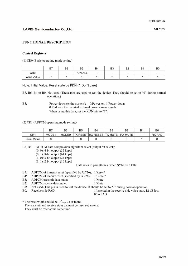
FUNCTIONAL DESCRIPTION Control Registers (1) CR0 (Basic operating mode setting)
B7 B6 B5 B4 B3 B2 B1 B0
CR0 — — PDN ALL — — — — —
Initial Value * * 0 * * * * *
Note: Initial Value: Reset state by PDN (*: Don’t care) B7, B6, B4 to B0: Not used (These pins are used to test the device. They should be set to “0” during normal
operation.) B5: Power-down (entire system); 0/Power-on, 1/Power-down 0 Red with the inverted external power-down signals. When using this data, set the RDN pin to “1”. (2) CR1 (ADPCM operating mode setting)
B7 B6 B5 B4 B3 B2 B1 B0
CR1 MODE1 MODE0 TX RESET RX RESET TX MUTE RX MUTE — RX PAD
Initial Value 0 0 0 0 0 0 * 0
B7, B6: ADPCM data compression algorithm select (output bit select);
(0, 0): 4-bit output (32 kbps) (0, 1): 8-bit output (64 kbps) (1, 0): 3-bit output (24 kbps) (1, 1): 2-bit output (16 kbps) Data rates in parentheses: when SYNC = 8 kHz
B5: ADPCM of transmit reset (specified by G.726); 1/Reset* B4: ADPCM of receive reset (specified by G.726); 1/ Reset* B3: ADPCM transmit data mute; 1/Mute B2: ADPCM receive data mute; 1/Mute B1: Not used (This pin is used to test the device. It should be set to “0” during normal operation. B0: Receive side PAD; 1/inserted in the receive side voice path, 12 dB loss 0/no PAD * The reset width should be 1/f sample s or more. The transmit and receive sides cannnot be reset separately.
They must be reset at the same time.
FEDL7029-04
ML7029
17/29
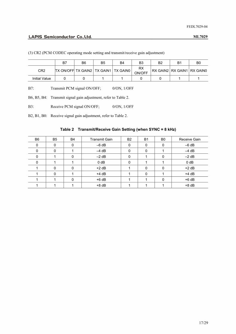
(3) CR2 (PCM CODEC operating mode setting and transmit/receive gain adjustment)
B7 B6 B5 B4 B3 B2 B1 B0
CR2 TX ON/OFF TX GAIN2 TX GAIN1 TX GAIN0RX
ON/OFFRX GAIN2 RX GAIN1 RX GAIN0
Initial Value 0 0 1 1 0 0 1 1
B7: Transmit PCM signal ON/OFF; 0/ON, 1/OFF B6, B5, B4: Transmit signal gain adjustment, refer to Table 2. B3: Receive PCM signal ON/OFF; 0/ON, 1/OFF B2, B1, B0: Receive signal gain adjustment, refer to Table 2.
Table 2 Transmit/Receive Gain Setting (when SYNC = 8 kHz)
B6 B5 B4 Transmit Gain B2 B1 B0 Receive Gain
0 0 0 –6 dB 0 0 0 –6 dB
0 0 1 –4 dB 0 0 1 –4 dB
0 1 0 –2 dB 0 1 0 –2 dB
0 1 1 0 dB 0 1 1 0 dB
1 0 0 +2 dB 1 0 0 +2 dB
1 0 1 +4 dB 1 0 1 +4 dB
1 1 0 +6 dB 1 1 0 +6 dB
1 1 1 +8 dB 1 1 1 +8 dB

FEDL7029-04
ML7029
18/29
(4) CR3 (Side tone gain setting)
B7 B6 B5 B4 B3 B2 B1 B0
CR3 Side Tone
GAIN2 Side Tone
GAIN1 Side Tone
GAIN0 — — —
HPF 8k/11k
HPF ON/OFF
Initial Value 0 0 0 * * * 0 0
B7, B6, B5: Side tone path gain setting. Refer to Table 3. B4 to B2: Not used (These pins are used to test the device. They should be set to “0” during normal operation.)
Table 3 Side Tone Pash Gain Setting (when SYNC = 8 kHz)
B7 B6 B5 Side Tone Path Gain
0 0 0 OFF
0 0 1 –21 dB
0 1 0 –19 dB
0 1 1 –17 dB
1 0 0 –15 dB
1 0 1 –13 dB
1 1 0 –11 dB
1 1 1 –9 dB
B1: Transmit HPF cut-off frequency select; 0/The cut-off frequency of the transmit HPF is the sampling frequency 0.0275. When SYNC = 8 kHz: 220 Hz, when SYNC = 11.025 kHz: 300 Hz. The transmit frequency characteristics are not guaranteed when selecting SYNC = 11.025 kHz. 1/The cut-off frequency of the transmit HPF is the sampling frequency 0.0200. When SYNC = 8 kHz: 160 Hz, when SYNC = 11.025 kHz: 220 Hz. The transmit frequency characteristics are not guaranteed when selecting SYNC = 8 kHz. B0: Transmit HPF ON/OFF; 0/ON, 1/OFF For the frequency characteristics, refer to Figures 9 to 12 in the Reference Data.
FEDL7029-04
ML7029
19/29
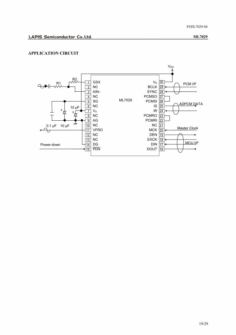
APPLICATION CIRCUIT
1
2
3
4
5
6
7
8
9
10
11
12
13
14
15
30
29
28
27
26
25
24
23
22
21
20
19
18
17
16
GSX NC AIN– NC SG NC VA NC AG NC VFRO NC NC DG PDN
VD
BCLKSYNC
PCMSOPCMSI
ISIR
PCMROPCMRI
NCMCKDEN
EXCKDIN
DOUT
Master Clock
MCU I/F
PCM I/F
Power-down
R1
0.1 µF 10 µF
R2
ML7029 ADPCM DATA
10 µF
VDD
FEDL7029-04
ML7029
20/29
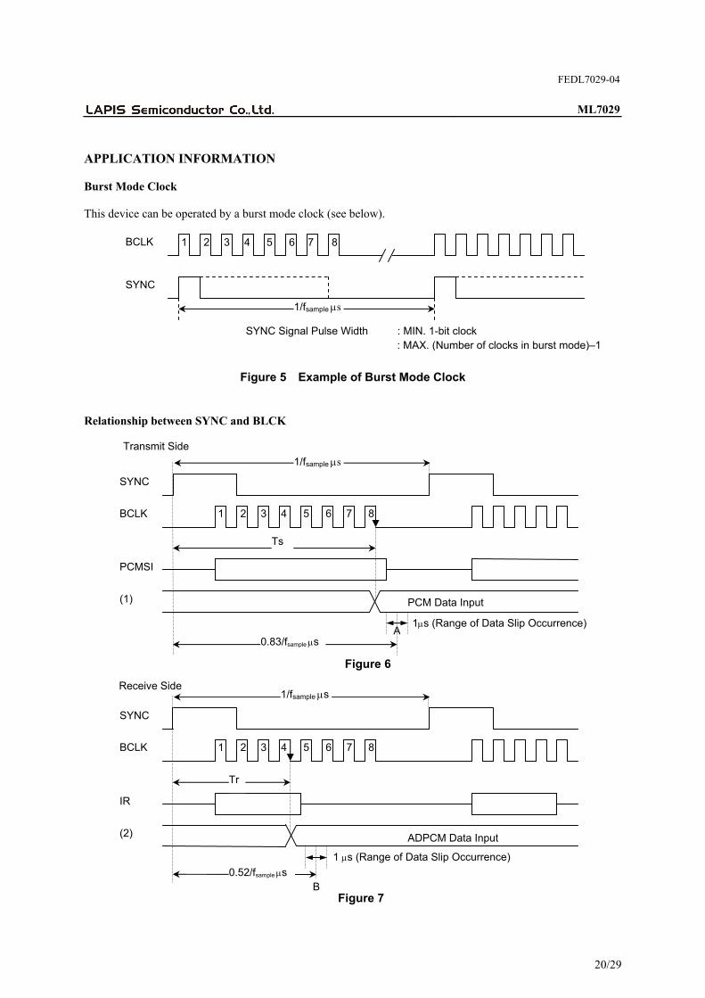
APPLICATION INFORMATION Burst Mode Clock This device can be operated by a burst mode clock (see below).
Figure 5 Example of Burst Mode Clock
Relationship between SYNC and BLCK
BFigure 7
SYNC
BCLK 1 2 3 4 5 6 7 8
IR
(2) ADPCM Data Input
0.52/fsample s
Receive Side
Tr
1 s (Range of Data Slip Occurrence)
1/fsample s
A
Figure 6
SYNC
BCLK 1 2 3 4 5 6 7 8
PCMSI
(1) PCM Data Input
0.83/fsample s
1s (Range of Data Slip Occurrence)
Transmit Side
Ts
1/fsample s
BCLK
SYNC
SYNC Signal Pulse Width : MIN. 1-bit clock : MAX. (Number of clocks in burst mode)–1
1 2 3 4 5 6 7 8
1/fsample s

FEDL7029-04
ML7029
21/29
(1): PCM data serial to parallel conversion output (2): ADPCM data serial to parallel conversion output A: (1) Data internal latch timing B: (2) Data internal latch timing
Figure 8 In this device, internal operating timing is generated according to the SYNC signal (see Figure 8). Therefore, a data slip may occur in the following timing when the PCM and ADPCM data is input. 1. When the PCM signal (PCMSI) is captured
If TS: PCM signal output (1) after serial/parallel conversion and A: internal latch timing in Figure 6 overlap, a data slip occurs.
2. When the ADPCM signal (IR) is captured
If Tr: ADPCM signal output (2) after serial/parallel conversion and B: internal latch timing in Figure 7 overlap, a data slip occurs.
The data slip occurs at the timing of 1 and 2 above. Therefore, taking internal clock jitters and IC internal delay into consideration, the timing of SYNC and BCLK signals should not be set up in the range of about 1 s from the timing A and B.
PCMSI IS
Internal Clock Generation
ADPCM COD S/P
A SYNC
BCLK
(1)
PCMRO IR ADPCM DEC P/S Latch
B
(2)
Latch
S/P
P/S Latch
Latch

FEDL7029-04
ML7029
22/29
REFERENCE DATA Transmit Frequency Characteristics
Figure 9 Transmit Bandpass Filter Characteristic (Fs = 8 kHz, CR3-B1, B0 = (0, 0))
Figure 10 Transmit Lowpass Filter Characteristic (Fs = 8 kHz, CR3-B1, B0 = (0, 1))
Fs = 8 kHz Transmit BPF Characteristic
-80
-70
-60
-50
-40
-30
-20
-10
0
10
100 1000 10000
Frequency (Hz)
Gai
n (d
B)
Fs = 8kHz Transmit LPF Characteristic
-80
-70
-60
-50
-40
-30
-20
-10
0
10
100 1000 10000
Frequency (Hz)
Gai
n (d
B)

FEDL7029-04
ML7029
23/29
Figure 11 Transmit Bandpass Filter Characteristic (Fs = 11.025 kHz, CR3-B1, B0 = (1, 0))
Figure 12 Transmit Lowpass Filter Characteristic (Fs = 11.025 kHz, CR3-B1, B0 = (1, 1))
Fs = 11.025 kHz Transmit BPF Characteristic
-80
-70
-60
-50
-40
-30
-20
-10
0
10
100 1000
Frequency (Hz)
Gai
n (d
B)
Fs = 11.025 kHz Transmit LPF Characteristic
-80
-70
-60
-50
-40
-30
-20
-10
0
10
100 1000
Frequency (Hz)
Gai
n (d
B)
10000
10000

FEDL7029-04
ML7029
24/29
Receive Frequency Characteristics
Figure 13 Receive Lowpass Filter Characteristic (Fs = 8 kHz, CR3-B1, B0 = (0, *))
Fs = 8 kHz Receive LPF Characteristic
-80
-70
-60
-50
-40
-30
-20
-10
0
10
100 1000 10000
Frequency (Hz)
Gai
n (d
B)
Figure 14 Receive Lowpass Filter Characteristic (Fs = 11.025 kHz, CR3-B1, B0 = (1, *))
Fs = 11.025 kHz Receive LPF Characteristic
-80
-70
-60
-50
-40
-30
-20
-10
0
10
100 1000
Frequency (Hz)
Gai
n (d
B)
10000

FEDL7029-04
ML7029
25/29
APPENDIX When the Sampling Frequency is 16 kHz or Higher: This device enables the operation at 16 kHz or higher sampling frequencies under conditions below. However, be aware that the AC characteristics are not guaranteed under these conditions. Operating Conditions at Sampling Frequency = 19 kHz
Parameter Symbol Condition Min. Typ. Max. Unit
Power Supply Voltage VDD Voltage must be fixed 3.0 — 3.6 V
Operating Temperature Range Ta — –25 — +50 C
Digital Input High Voltage VIH Digital input pin 0.95
VDD — VDD V
Digital Input Low Voltage VIL Digital input pin 0 0.05
VDD V
Master Clock Frequency fMCK1 MCK — 24.624 — MHz
Master Clock Frequency Accuracy fMCK2 MCK –0.01%SYNC
1296 +0.01 MHz
Sampling Frequency fSYNC SYNC — 19 — kHz
Master Clock Duty Ratio DMCK — 40 — 70 %
Transmit S/N Ratio (at 3 dBm0 input)
SD19T1 — — 46.2 — dB
Transmit S/N Ratio (at –40 dBm0 input)
SD19T2 — — 24.8 — dB
Receive S/N Ratio (at 3 dBm0 input)
SD19R1 — — 45.4 — dB
Receive S/N Ratio (at –40 dBm0 input)
SD19R2 — — 38.0 — dB

FEDL7029-04
ML7029
26/29
Operating Conditions at Sampling Frequency = 21 kHz
Parameter Symbol Condition Min. Typ. Max. Unit
Power Supply Voltage VDD Voltage must be fixed 3.3 — 3.6 V
Operating Temperature Range Ta — –25 — +50 C
Digital Input High Voltage VIH Digital input pin 0.95
VDD — VDD V
Digital Input Low Voltage VIL Digital input pin 0 0.05
VDD V
Master Clock Frequency fMCK1 MCK — 27.216 — MHz
Master Clock Frequency Accuracy fMCK2 MCK –0.01%SYNC
1296 +0.01 MHz
Sampling Frequency fSYNC SYNC — 21 — kHz
Master Clock Duty Ratio DMCK — 40 — 70 %
Transmit S/N Ratio (at 3 dBm0 input)
SD19T1 — — 46.1 — dB
Transmit S/N Ratio (at –40 dBm0 input)
SD19T2 — — 20.2 — dB
Receive S/N Ratio (at 3 dBm0 input)
SD19R1 — — 44.8 — dB
Receive S/N Ratio (at –40 dBm0 input)
SD19R2 — — 37.8 — dB
FEDL7029-04
ML7029
27/29
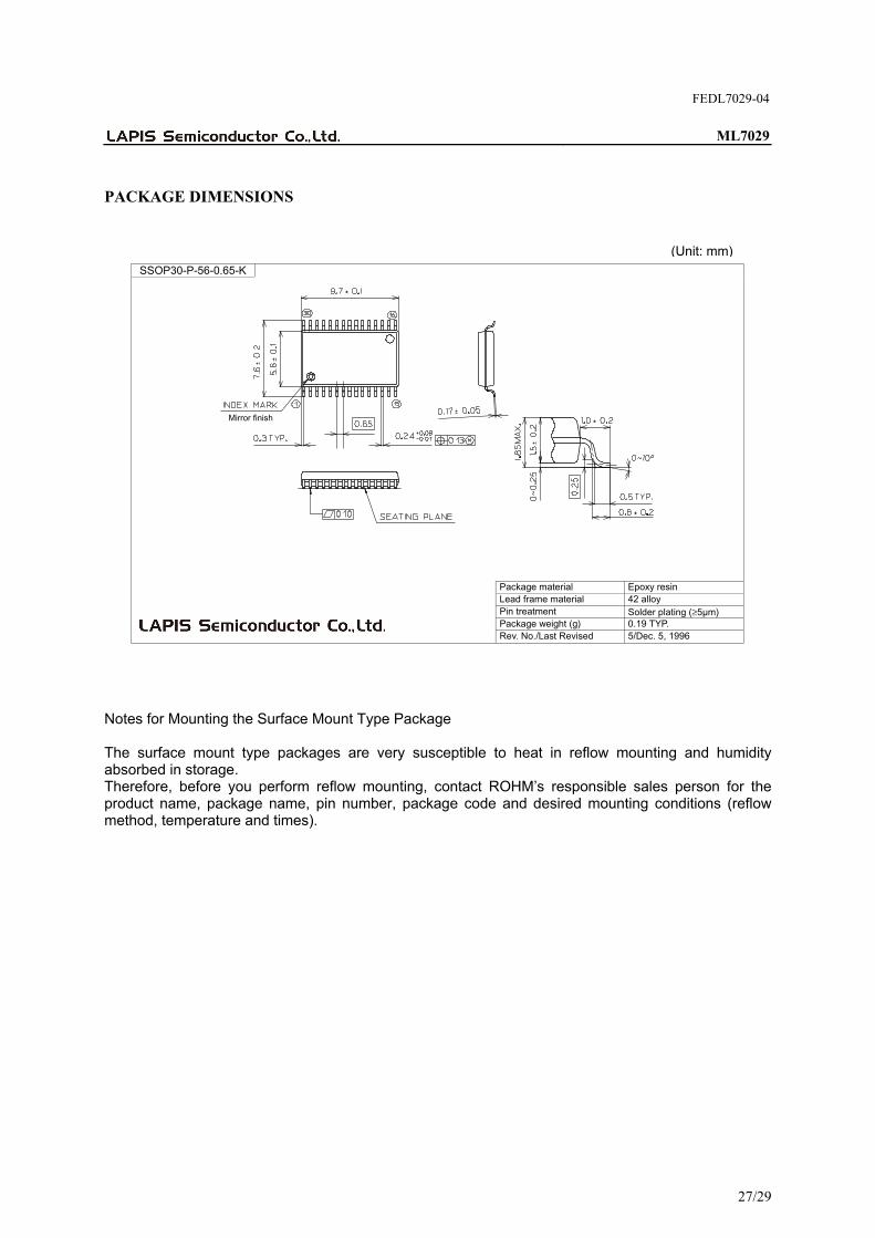
PACKAGE DIMENSIONS
Notes for Mounting the Surface Mount Type Package The surface mount type packages are very susceptible to heat in reflow mounting and humidity absorbed in storage. Therefore, before you perform reflow mounting, contact ROHM’s responsible sales person for the product name, package name, pin number, package code and desired mounting conditions (reflow method, temperature and times).
SSOP30-P-56-0.65-K
Mirror finish
Package material Epoxy resinLead frame material 42 alloyPin treatment Solder plating (≥5μm)Package weight (g) 0.19 TYP.5Rev. No./Last Revised 5/Dec. 5, 1996
(Unit: mm)
FEDL7029-04
ML7029
28/29
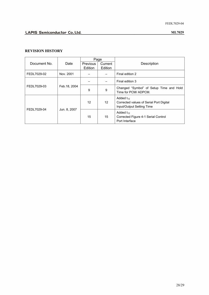
REVISION HISTORY
Page Document No. Date Previous
Edition CurrentEdition
Description
FEDL7029-02 Nov. 2001 – – Final edition 2
– – Final edition 3
FEDL7029-03 Feb.18, 2004 9 9
Changed “Symbol” of Setup Time and Hold Time for PCM/ ADPCM.
12 12 Added t12
Corrected values of Serial Port Digital Input/Output Setting Time
FEDL7029-04 Jun. 8, 2007
15 15 Added t12
Corrected Figure 4-1 Serial Control Port Interface
FEDL7029-04
ML7029
29/29
NOTES No copying or reproduction of this document, in part or in whole, is permitted without the consent of LAPIS Semiconductor Co., Ltd. The content specified herein is subject to change for improvement without notice. The content specified herein is for the purpose of introducing LAPIS Semiconductor's products (hereinafter "Products"). If you wish to use any such Product, please be sure to refer to the specifications, which can be obtained from LAPIS Semiconductor upon request. Examples of application circuits, circuit constants and any other information contained herein illustrate the standard usage and operations of the Products. The peripheral conditions must be taken into account when designing circuits for mass production. Great care was taken in ensuring the accuracy of the information specified in this document. However, should you incur any damage arising from any inaccuracy or misprint of such information, LAPIS Semiconductor shall bear no responsibility for such damage. The technical information specified herein is intended only to show the typical functions of and examples of application circuits for the Products. LAPIS Semiconductor does not grant you, explicitly or implicitly, any license to use or exercise intellectual property or other rights held by LAPIS Semiconductor and other parties. LAPIS Semiconductor shall bear no responsibility whatsoever for any dispute arising from the use of such technical information. The Products specified in this document are intended to be used with general-use electronic equipment or devices (such as audio visual equipment, office-automation equipment, communication devices, electronic appliances and amusement devices). The Products specified in this document are not designed to be radiation tolerant. While LAPIS Semiconductor always makes efforts to enhance the quality and reliability of its Products, a Product may fail or malfunction for a variety of reasons. Please be sure to implement in your equipment using the Products safety measures to guard against the possibility of physical injury, fire or any other damage caused in the event of the failure of any Product, such as derating, redundancy, fire control and fail-safe designs. LAPIS Semiconductor shall bear no responsibility whatsoever for your use of any Product outside of the prescribed scope or not in accordance with the instruction manual. The Products are not designed or manufactured to be used with any equipment, device or system which requires an extremely high level of reliability the failure or malfunction of which may result in a direct threat to human life or create a risk of human injury (such as a medical instrument, transportation equipment, aerospace machinery, nuclear-reactor controller, fuel-controller or other safety device). LAPIS Semiconductor shall bear no responsibility in any way for use of any of the Products for the above special purposes. If a Product is intended to be used for any such special purpose, please contact a ROHM sales representative before purchasing. If you intend to export or ship overseas any Product or technology specified herein that may be controlled under the Foreign Exchange and the Foreign Trade Law, you will be required to obtain a license or permit under the Law.
Copyright 2011 LAPIS Semiconductor Co., Ltd.