Features Description - Diodes Incorporated power consumption to support Energy Star Compliance ESD...
15
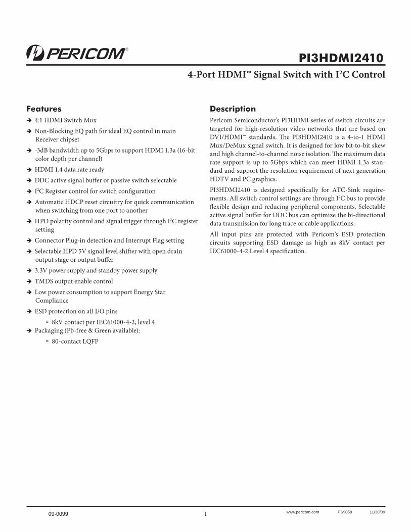
1 www.pericom.com PS9058 11/30/09 PI3HDMI2410 Description Pericom Semiconductor’s PI3HDMI series of switch circuits are targeted for high-resolution video networks that are based on DVI/HDMI™ standards. e PI3HDMI2410 is a 4-to-1 HDMI Mux/DeMux signal switch. It is designed for low bit-to-bit skew and high channel-to-channel noise isolation. e maximum data rate support is up to 5Gbps which can meet HDMI 1.3a stan- dard and support the resolution requirement of next generation HDTV and PC graphics. PI3HDMI2410 is designed specifically for ATC-Sink require- ments. All switch control settings are through I 2 C bus to provide flexible design and reducing peripheral components. Selectable active signal buffer for DDC bus can optimize the bi-directional data transmission for long trace or cable applications. All input pins are protected with Pericom’s ESD protection circuits supporting ESD damage as high as 8kV contact per IEC61000-4-2 Level 4 specification. Features 4:1 HDMI Switch Mux Non-Blocking EQ path for ideal EQ control in main Receiver chipset -3dB bandwidth up to 5Gbps to support HDMI 1.3a (16-bit color depth per channel) HDMI 1.4 data rate ready DDC active signal buffer or passive switch selectable I 2 C Register control for switch configuration Automatic HDCP reset circuitry for quick communication when switching from one port to another HPD polarity control and signal trigger through I 2 C register setting Connector Plug-in detection and Interrupt Flag setting Selectable HPD 5V signal level shiſter with open drain output stage or output buffer 3.3V power supply and standby power supply TMDS output enable control Low power consumption to support Energy Star Compliance ESD protection on all I/O pins 8kV contact per IEC61000-4-2, level 4 Packaging (Pb-free & Green available): 80-contact LQFP 4-Port HDMI™ Signal Switch with I 2 C Control 09-0099
Transcript of Features Description - Diodes Incorporated power consumption to support Energy Star Compliance ESD...
1 www.pericom.com PS9058 11/30/09
PI3HDMI2410
DescriptionPericom Semiconductor’s PI3HDMI series of switch circuits are targeted for high-resolution video networks that are based on DVI/HDMI™ standards. Th e PI3HDMI2410 is a 4-to-1 HDMI Mux/DeMux signal switch. It is designed for low bit-to-bit skew and high channel-to-channel noise isolation. Th e maximum data rate support is up to 5Gbps which can meet HDMI 1.3a stan-dard and support the resolution requirement of next generation HDTV and PC graphics.PI3HDMI2410 is designed specifi cally for ATC-Sink require-ments. All switch control settings are through I2C bus to provide fl exible design and reducing peripheral components. Selectable active signal buff er for DDC bus can optimize the bi-directional data transmission for long trace or cable applications. All input pins are protected with Pericom’s ESD protection circuits supporting ESD damage as high as 8kV contact per IEC61000-4-2 Level 4 specifi cation.
Features 4:1 HDMI Switch Mux Non-Blocking EQ path for ideal EQ control in main
Receiver chipset -3dB bandwidth up to 5Gbps to support HDMI 1.3a (16-bit
color depth per channel) HDMI 1.4 data rate ready DDC active signal buff er or passive switch selectable I2C Register control for switch confi guration Automatic HDCP reset circuitry for quick communication
when switching from one port to another HPD polarity control and signal trigger through I2C register
setting Connector Plug-in detection and Interrupt Flag setting Selectable HPD 5V signal level shift er with open drain
output stage or output buff er 3.3V power supply and standby power supply TMDS output enable control Low power consumption to support Energy Star
Compliance ESD protection on all I/O pins
8kV contact per IEC61000-4-2, level 4 Packaging (Pb-free & Green available):
80-contact LQFP
4-Port HDMI™ Signal Switch with I2C Control
09-0099
2 www.pericom.com PS9058 11/30/09
PI3HDMI24104-Port HDMI™ Signal Switch with I2C Control
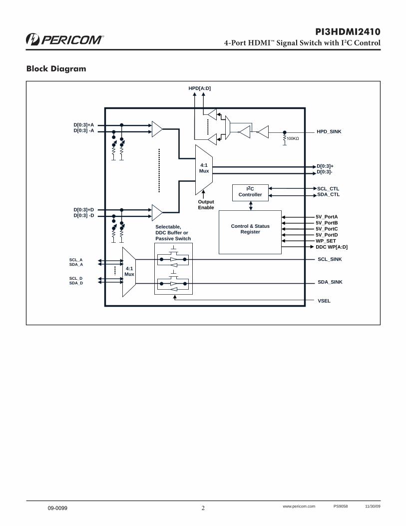
Block Diagram
4:1 Mux
SCL_A SDA_A SCL_D SDA_D
D[0:3]+A D[0:3] -A
D[0:3]+D D[0:3] -D
Selectable,DDC Buffer orPassive Switch
D[0:3]+ D[0:3]-
HPD_SINK
4:1 Mux
HPD[A:D]
Output Enable
100K
Control & Status Register
I2C Controller
SCL_CTL SDA_CTL
SCL_SINK
SDA_SINK
VSEL
5V_PortA5V_PortB5V_PortC5V_PortDWP_SETDDC WP[A:D]
09-0099
3 www.pericom.com PS9058 11/30/09
PI3HDMI24104-Port HDMI™ Signal Switch with I2C Control
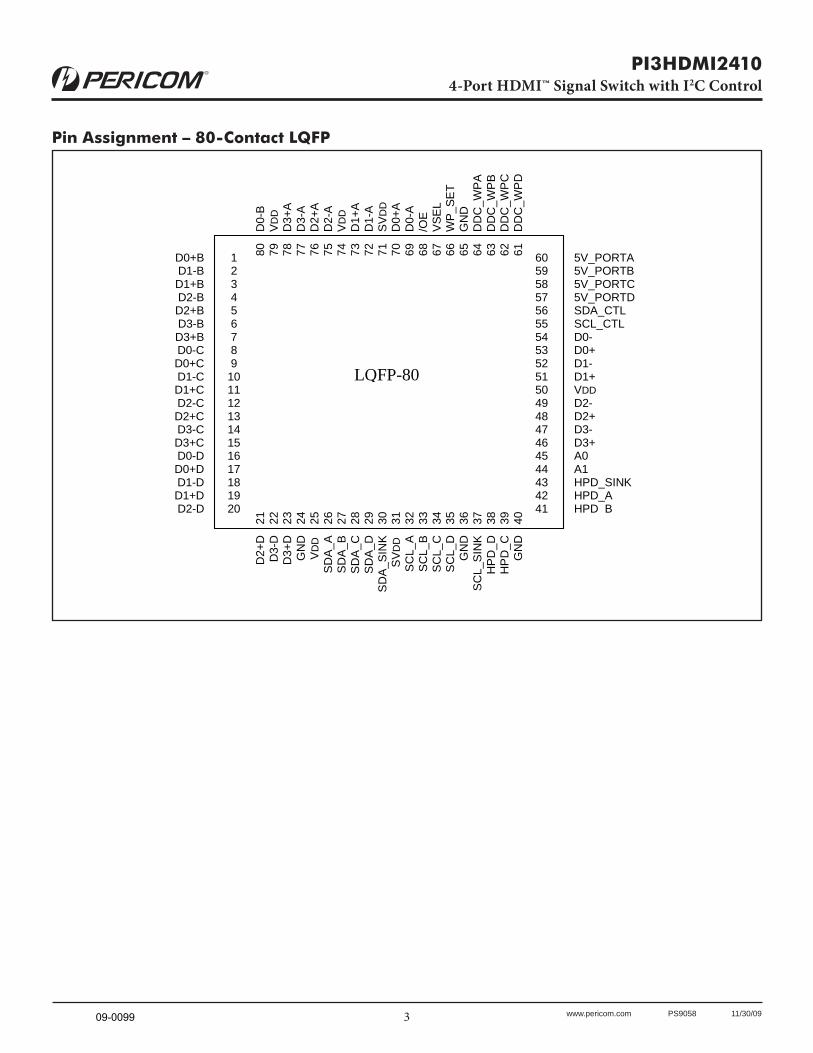
Pin Assignment – 80-Contact LQFP
1 2 3 4 5 6 7 8 9
10 11 12 13 14 15 16 17 18 19 20
60 59 58 57 56 55 54 53 52 51 50 49 48 47 46 45 44 43 42 41
21
22
23
24
25
26
27
28
29
30
31
32
33
34
35
36
37
38
39
40
80
79
78
77
76
75
74
73
72
71
70
69
68
67
66
65
64
63
62
61
D0+B D1-B D1+B D2-B D2+B D3-B D3+B D0-C D0+C D1-C D1+C D2-C D2+C D3-C D3+C D0-D D0+D D1-D D1+D D2-D
5V_PORTA 5V_PORTB 5V_PORTC 5V_PORTD SDA_CTL SCL_CTL D0- D0+ D1- D1+ VDD D2- D2+ D3- D3+ A0 A1 HPD_SINK HPD_A HPD B
D2+
DD
3-D
D3+
DG
ND
VD
DS
DA
_AS
DA
_BS
DA
_CS
DA
_DS
DA
_SIN
KS
VD
DS
CL_
AS
CL_
BS
CL_
CS
CL_
DG
ND
SC
L_S
INK
HP
D_D
HP
D_C
GN
D
D0-
B
VD
D
D3+
A
D3-
A
D2+
A
D2-
A
VD
D
D1+
A
D1-
A
SV
DD
D
0+A
D
0-A
/O
E
VSE
L W
P_S
ET
GN
D
DD
C_W
PA
D
DC
_WP
B
DD
C_W
PC
D
DC
_WP
D
LQFP-80
09-0099
4 www.pericom.com PS9058 11/30/09
PI3HDMI24104-Port HDMI™ Signal Switch with I2C Control
Pinout Table
Pin Name I/O Type Description
VDD I/O 3.3V power supply. When VDD is off , the TMDS channels will be powered down.
SVDD I/O 3.3V standby power supply. SVDD is for all side band signals, I2C register and I2C bus.
HPD_SINK ISink side hot plug detector input. High: 5-V power signal asserted from source to sink and EDID is ready. Low: No 5-V power signal asserted from source to sink, or EDID is not ready.
HPD_A O Port A HPD output
HPD_B O Port B HPD output
HPD_C O Port C HPD output
HPD_D O Port D HPD output
D0+AD0-AD1+AD1-AD2+AD2-AD3+AD3-A
I Port A TMDS inputs
D0+BD0-BD1+BD1-BD2+BD2-BD3+BD3-B
I Port B TMDS inputs
D0+CD0-CD1+CD1-CD2+CD2-CD3+CD3-C
I Port C TMDS inputs
09-0099
5 www.pericom.com PS9058 11/30/09
PI3HDMI24104-Port HDMI™ Signal Switch with I2C Control
Pin Name I/O Type DescriptionD0+DD0-DD1+DD1-DD2+DD2-DD3+DD3-D
I Port D TMDS inputs
D0+D0-D1+D1-D2+D2-D3+D3-
O TMDS outputs
SCL_A I/O Port A DDC Clock
SCL_B I/O Port B DDC Clock
SCL_C I/O Port C DDC Clock
SCL_D I/O Port D DDC Clock
SDA_A I/O Port A DDC Data
SDA_B I/O Port B DDC Data
SDA_C I/O Port C DDC Data
SDA_D I/O Port D DDC Data
SCL_SINK I/O Sink side DDC Clock
SDA_SINK I/O Sink side DDC Data
SCL_CTL I/O I2C Clock
SDA_CTL I/O I2C Data
WP_SET IWP_SET = 0 (Default), Set B1b[1] as INT Flag.WP_SET = 1, DDC_WP[A:D] is programmable by B1b[1].
DDC_WPA,DDC_WPB,DDC_WPC,DDC_WPD,
O Open drain output. When WP_SET = 1, general purpose logic confi gured by B1b[1]
OE I Output Enable control. Active low.
A1 I I2C Address 1
A0 I I2C Address 0
09-0099
6 www.pericom.com PS9058 11/30/09
PI3HDMI24104-Port HDMI™ Signal Switch with I2C Control
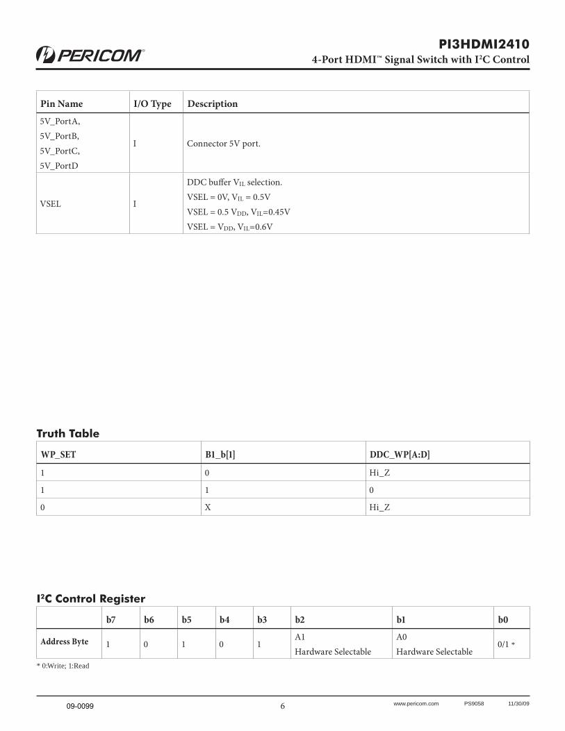
Pin Name I/O Type Description5V_PortA, 5V_PortB, 5V_PortC, 5V_PortD
I Connector 5V port.
VSEL I
DDC buff er VIL selection. VSEL = 0V, VIL = 0.5VVSEL = 0.5 VDD, VIL=0.45VVSEL = VDD, VIL=0.6V
Truth Table
WP_SET B1_b[1] DDC_WP[A:D]
1 0 Hi_Z
1 1 0
0 X Hi_Z
I2C Control Register
b7 b6 b5 b4 b3 b2 b1 b0
Address Byte 1 0 1 0 1 A1 Hardware Selectable
A0 Hardware Selectable
0/1 *
* 0:Write; 1:Read
09-0099
7 www.pericom.com PS9058 11/30/09
PI3HDMI24104-Port HDMI™ Signal Switch with I2C Control
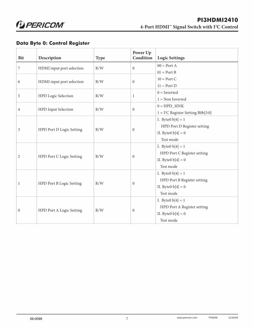
Data Byte 0: Control Register
Bit Description TypePower Up Condition Logic Settings
7 HDMI input port selection R/W 0 00 = Port A 01 = Port B 10 = Port C 11 = Port D
6 HDMI input port selection R/W 0
5 HPD Logic Selection R/W 10 = Inverted 1 = Non Inverted
4 HPD Input Selection R/W 00 = HPD_SINK 1 = I2C Register Setting B0b[3:0]
3 HPD Port D Logic Setting R/W 0
I. Byte0 b[4] = 1 HPD Port D Register setting II. Byte0 b[4] = 0 Test mode
2 HPD Port C Logic Setting R/W 0
I. Byte0 b[4] = 1 HPD Port C Register setting II. Byte0 b[4] = 0 Test mode
1 HPD Port B Logic Setting R/W 0
I. Byte0 b[4] = 1 HPD Port B Register setting II. Byte0 b[4] = 0 Test mode
0 HPD Port A Logic Setting R/W 0
I. Byte0 b[4] = 1 HPD Port A Register setting II. Byte0 b[4] = 0 Test mode
09-0099
8 www.pericom.com PS9058 11/30/09
PI3HDMI24104-Port HDMI™ Signal Switch with I2C Control
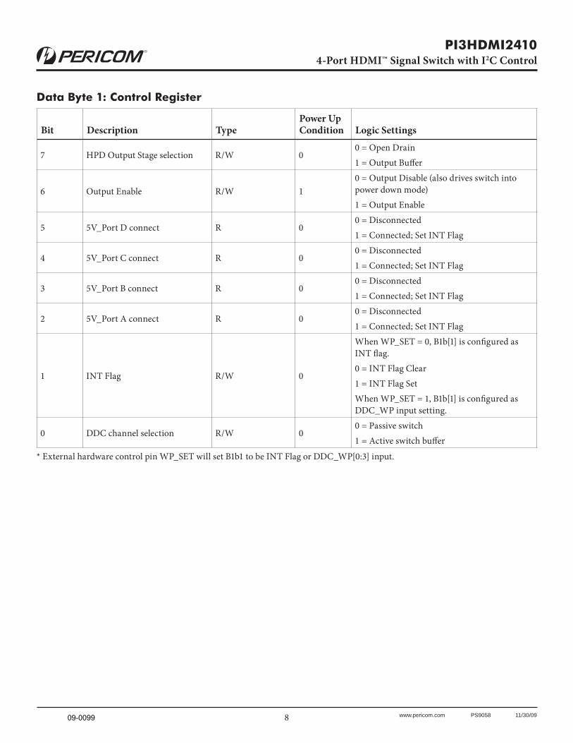
Data Byte 1: Control Register
Bit Description TypePower Up Condition Logic Settings
7 HPD Output Stage selection R/W 00 = Open Drain 1 = Output Buff er
6 Output Enable R/W 10 = Output Disable (also drives switch into power down mode) 1 = Output Enable
5 5V_Port D connect R 00 = Disconnected 1 = Connected; Set INT Flag
4 5V_Port C connect R 00 = Disconnected 1 = Connected; Set INT Flag
3 5V_Port B connect R 00 = Disconnected 1 = Connected; Set INT Flag
2 5V_Port A connect R 00 = Disconnected 1 = Connected; Set INT Flag
1 INT Flag R/W 0
When WP_SET = 0, B1b[1] is confi gured as INT fl ag. 0 = INT Flag Clear 1 = INT Flag Set When WP_SET = 1, B1b[1] is confi gured as DDC_WP input setting.
0 DDC channel selection R/W 00 = Passive switch1 = Active switch buff er
* External hardware control pin WP_SET will set B1b1 to be INT Flag or DDC_WP[0:3] input.
09-0099
9 www.pericom.com PS9058 11/30/09
PI3HDMI24104-Port HDMI™ Signal Switch with I2C Control
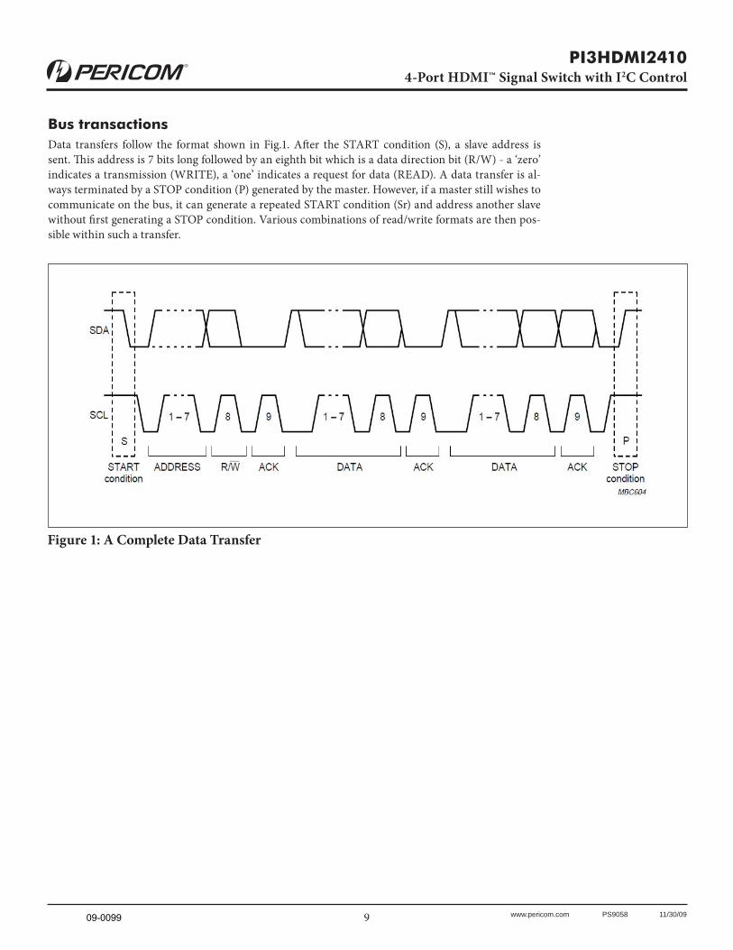
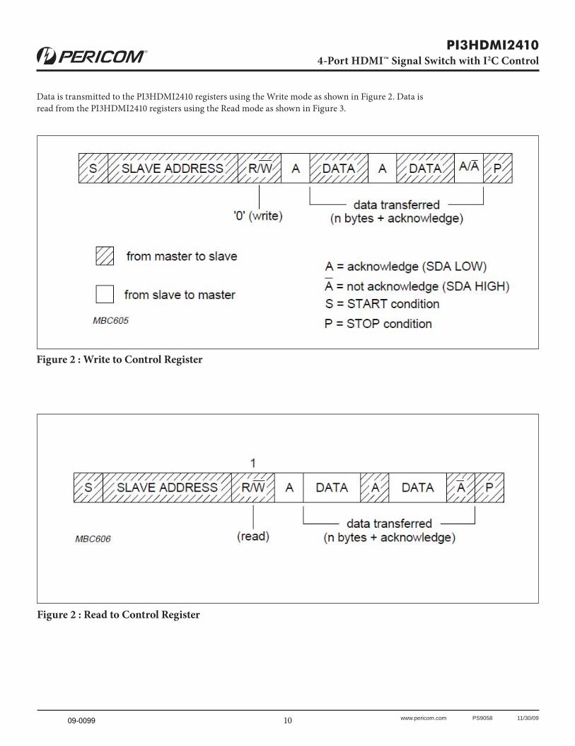
Bus transactionsData transfers follow the format shown in Fig.1. Aft er the START condition (S), a slave address is sent. Th is address is 7 bits long followed by an eighth bit which is a data direction bit (R/W) - a ‘zero’ indicates a transmission (WRITE), a ‘one’ indicates a request for data (READ). A data transfer is al-ways terminated by a STOP condition (P) generated by the master. However, if a master still wishes to communicate on the bus, it can generate a repeated START condition (Sr) and address another slave without fi rst generating a STOP condition. Various combinations of read/write formats are then pos-sible within such a transfer.
Figure 1: A Complete Data Transfer
09-0099
10 www.pericom.com PS9058 11/30/09
PI3HDMI24104-Port HDMI™ Signal Switch with I2C Control
Figure 2 : Write to Control Register
Figure 2 : Read to Control Register
Data is transmitted to the PI3HDMI2410 registers using the Write mode as shown in Figure 2. Data is read from the PI3HDMI2410 registers using the Read mode as shown in Figure 3.
09-0099
11 www.pericom.com PS9058 11/30/09
PI3HDMI24104-Port HDMI™ Signal Switch with I2C Control
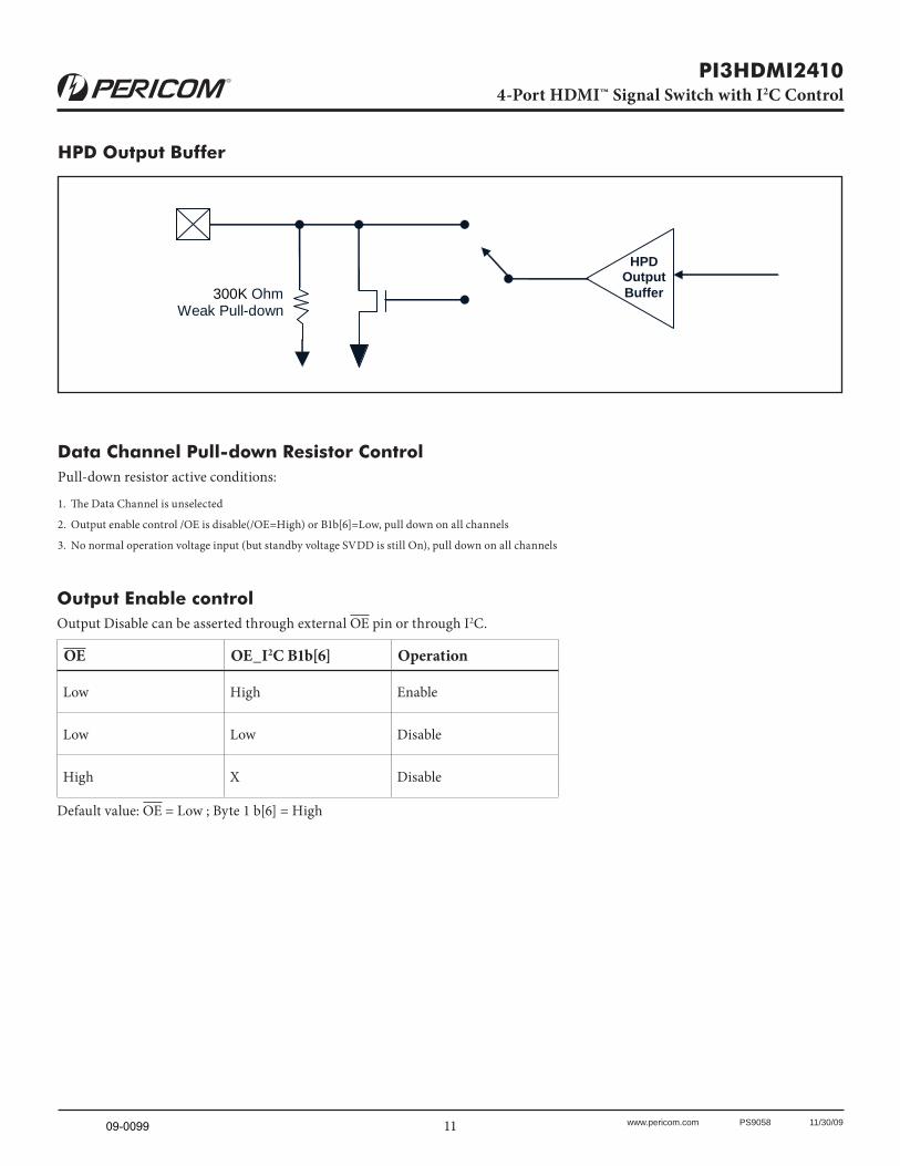
Data Channel Pull-down Resistor ControlPull-down resistor active conditions:
1. Th e Data Channel is unselected
2. Output enable control /OE is disable(/OE=High) or B1b[6]=Low, pull down on all channels
3. No normal operation voltage input (but standby voltage SVDD is still On), pull down on all channels
Output Enable controlOutput Disable can be asserted through external OE pin or through I2C.
OE OE_I2C B1b[6] Operation
Low High Enable
Low Low Disable
High X Disable
Default value: OE = Low ; Byte 1 b[6] = High
HPD Output Buffer
HPD Output Buffer 300K Ohm
Weak Pull-down
09-0099
12 www.pericom.com PS9058 11/30/09
PI3HDMI24104-Port HDMI™ Signal Switch with I2C Control
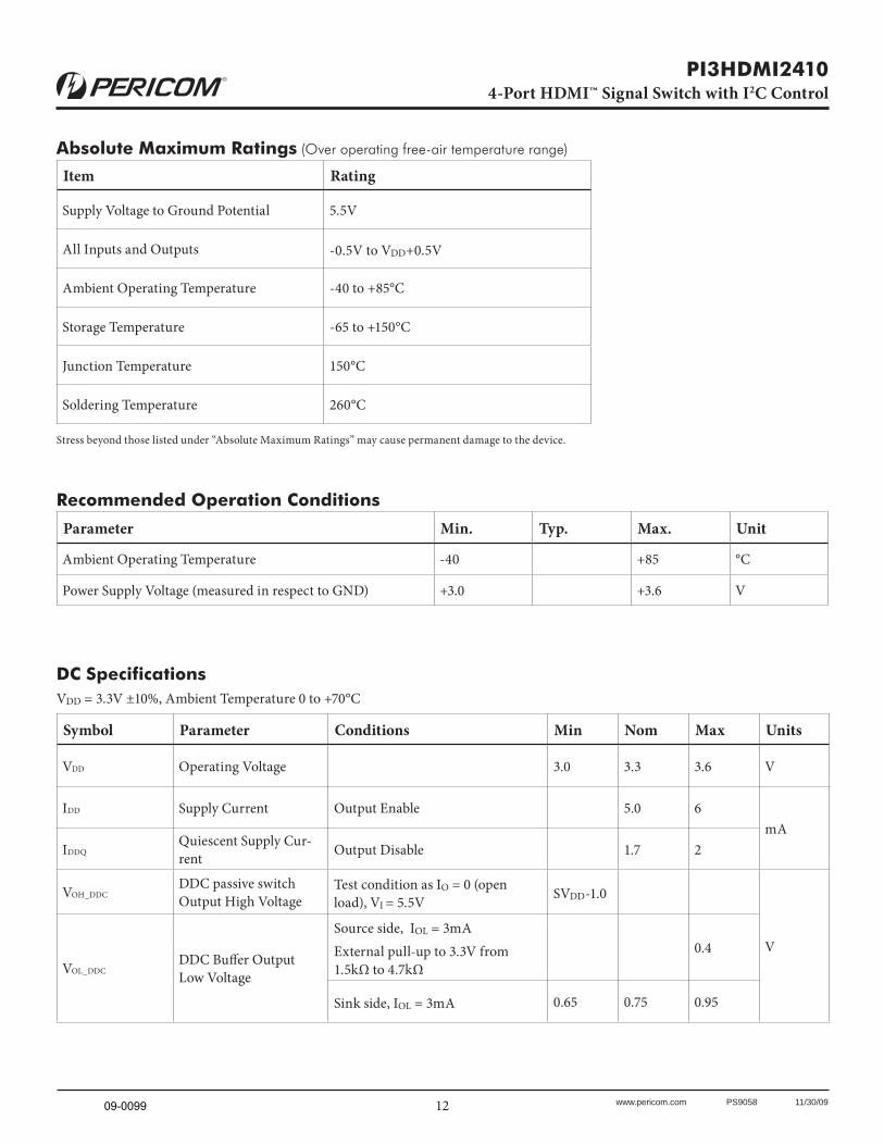
DC SpecificationsVDD = 3.3V ±10%, Ambient Temperature 0 to +70°C
Symbol Parameter Conditions Min Nom Max Units
VDD Operating Voltage 3.0 3.3 3.6 V
IDD Supply Current Output Enable 5.0 6mA
IDDQQuiescent Supply Cur-rent Output Disable 1.7 2
VOH_DDCDDC passive switch Output High Voltage
Test condition as IO = 0 (open load), VI = 5.5V SVDD-1.0
VVOL_DDC
DDC Buff er Output Low Voltage
Source side, IOL = 3mAExternal pull-up to 3.3V from 1.5kΩ to 4.7kΩ
0.4
Sink side, IOL = 3mA 0.65 0.75 0.95
Absolute Maximum Ratings (Over operating free-air temperature range)
Item Rating
Supply Voltage to Ground Potential 5.5V
All Inputs and Outputs -0.5V to VDD+0.5V
Ambient Operating Temperature -40 to +85°C
Storage Temperature -65 to +150°C
Junction Temperature 150°C
Soldering Temperature 260°C
Stress beyond those listed under “Absolute Maximum Ratings” may cause permanent damage to the device.
Recommended Operation Conditions
Parameter Min. Typ. Max. Unit
Ambient Operating Temperature -40 +85 °C
Power Supply Voltage (measured in respect to GND) +3.0 +3.6 V
09-0099
13 www.pericom.com PS9058 11/30/09
PI3HDMI24104-Port HDMI™ Signal Switch with I2C Control
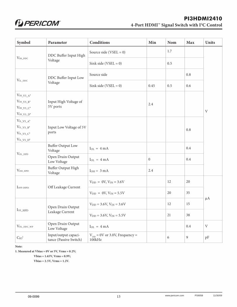
Symbol Parameter Conditions Min Nom Max Units
VIH_DDCDDC Buff er Input High Voltage
Source side (VSEL = 0) 1.7
V
Sink side (VSEL = 0) 0.5
VIL_DDCDDC Buff er Input Low Voltage
Source side 0.8
Sink side (VSEL = 0) 0.45 0.5 0.6
VIH_V5_A,
VIH_V5_B,
VIH_V5_C,
VIH_V5_D,
Input High Voltage of 5V ports 2.4
VIL_V5_A,
VIL_V5_B,
VIL_V5_C,
VIL_V5_D,
Input Low Voltage of 5V ports 0.8
VOL_HPD
Buff er Output Low Voltage IOL = 4 mA 0.4
Open Drain Output Low Voltage IOL = 4 mA 0 0.4
VOH_HPDBuff er Output High Voltage IOH = 3 mA 2.4
IOFF (HPD) Off Leakage CurrentVDD = 0V, VIN = 3.6V 12 20
μAVDD = 0V, VIN = 5.5V 20 35
IOZ_HPDOpen Drain Output Leakage Current
VDD = 3.6V, VIN = 3.6V 12 15
VDD = 3.6V, VIN = 5.5V 21 38
VOL_DDC_WPOpen Drain Output Low Voltage IOL = 4 mA 0.4 V
CIO1 Input/output capaci-tance (Passive Switch)
VDD = 0V or 3.0V, Frequency = 100kHz 6 9 pF
Note:1. Measured at Vbias = 0V or 5V, Vrms = 0.2V; Vbias = 1.65V, Vrms = 0.9V; Vbias = 2.5V, Vrms = 1.2V.
09-0099
14 www.pericom.com PS9058 11/30/09
PI3HDMI24104-Port HDMI™ Signal Switch with I2C Control
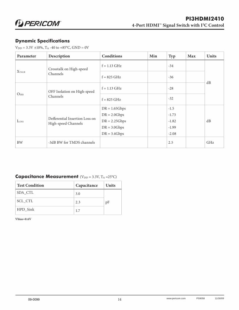
Dynamic SpecificationsVDD = 3.3V ±10%, TA -40 to +85°C, GND = 0V
Parameter Description Conditions Min Typ Max Units
XTALKCrosstalk on High-speed Channels
f = 1.13 GHz -34
dBf = 825 GHz -36
OIRROFF Isolation on High-speed Channels
f = 1.13 GHz -28
f = 825 GHz -32
ILOSSDeff erential Insertion Loss on High-speed Channels
DR = 1.65GbpsDR = 2.0GbpsDR = 2.25GbpsDR = 3.0GbpsDR = 3.4Gbps
-1.5-1.73-1.82-1.99-2.08
dB
BW -3dB BW for TMDS channels 2.5 GHz
Capacitance Measurement (VDD = 3.3V, TA =25°C)
Test Condition Capacitance UnitsSDA_CTL 3.0
pFSCL_CTL 2.3
HPD_Sink 1.7
Vbias=0.6V
09-0099
15 www.pericom.com PS9058 11/30/09
PI3HDMI24104-Port HDMI™ Signal Switch with I2C Control
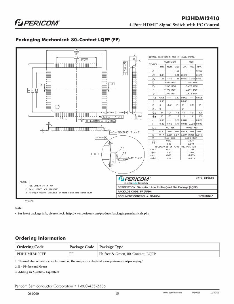
Packaging Mechanical: 80-Contact LQFP (FF)
DESCRIPTION: 80-contact, Low Profi le Quad Flat Package (LQFP)PACKAGE CODE: FF (FF80)
DOCUMENT CONTROL #: PD-2064 REVISION: A
DATE: 03/18/09
07-0100
Ordering Information
Ordering Code Package Code Package TypePI3HDMI2410FFE FF Pb-free & Green, 80-Contact, LQFP
1. Th ermal characteristics can be found on the company web site at www.pericom.com/packaging/
2. E = Pb-free and Green
3. Adding an X suffi x = Tape/Reel
Pericom Semiconductor Corporation • 1-800-435-2336
Note:
• For latest package info, please check: http://www.pericom.com/products/packaging/mechanicals.php
09-0099