FEATURES DESCRIPTIO U - analog.com · 1 LT1956/LT1956-5 1956f High Voltage, 1.5A, 500kHz Step-Down...
28
1 LT1956/LT1956-5 1956f High Voltage, 1.5A, 500kHz Step-Down Switching Regulators ■ Wide Input Range: 5.5V to 60V ■ 1.5A Peak Switch Current ■ Small 16-Pin SSOP or Thermally Enhanced TSSOP Package ■ Saturating Switch Design: 0.2Ω ■ Peak Switch Current Maintained Over Full Duty Cycle Range ■ Constant 500kHz Switching Frequency ■ Effective Supply Current: 2.5mA ■ Shutdown Current: 25μ A ■ 1.2V Feedback Reference (LT1956) ■ 5V Fixed Output (LT1956-5) ■ Easily Synchronizable ■ Cycle-by-Cycle Current Limiting The LT ® 1956/LT1956-5 are 500kHz monolithic buck switching regulators with an input voltage capability up to 60V. A high efficiency 1.5A, 0.2Ω switch is included on the die along with all the necessary oscillator, control and logic circuitry. A current mode architecture provides fast tran- sient response and good loop stability. Special design techniques and a new high voltage process achieve high efficiency over a wide input range. Efficiency is maintained over a wide output current range by using the output to bias the circuitry and by utilizing a supply boost capacitor to saturate the power switch. Patented circuitry maintains peak switch current over the full duty cycle range*. A shutdown pin reduces supply current to 25μ A and the device can be externally synchronized from 580kHz to 700kHz with a logic level input. The LT1956/LT1956-5 are available in fused-lead 16-pin SSOP and thermally enhanced TSSOP packages. ■ High Voltage, Industrial and Automotive ■ Portable Computers ■ Battery-Powered Systems ■ Battery Chargers ■ Distributed Power Systems , LTC and LT are registered trademarks of Linear Technology Corporation. 5V Buck Converter Efficiency vs Load Current BOOST V IN 6 2 10 12 10MQ060N V OUT 5V 1A 4 15 14 11 220pF 4700pF † UNITED CHEMI-CON THCS50EZA225ZT 1, 8, 9, 16 LT1956-5 SHDN SYNC SW BIAS FB V C GND 0.1μF 22μF 6.3V CERAMIC 10μH MMSD914TI 1956 TA01 2.2μF † 100V CERAMIC V IN 12V (TRANSIENTS TO 60V) 4.7k LOAD CURRENT (A) 0 EFFICIENCY (%) 80 90 100 1.00 1956 TA02 70 60 50 0.25 0.50 0.75 1.25 V OUT = 5V V OUT = 3.3V V IN = 12V L = 18μH DESCRIPTIO U FEATURES APPLICATIO S U TYPICAL APPLICATIO U *U.S. PATENT NO. 6,498,466
Transcript of FEATURES DESCRIPTIO U - analog.com · 1 LT1956/LT1956-5 1956f High Voltage, 1.5A, 500kHz Step-Down...

1
LT1956/LT1956-5
1956f
High Voltage, 1.5A,500kHz Step-Down
Switching Regulators
Wide Input Range: 5.5V to 60V 1.5A Peak Switch Current Small 16-Pin SSOP or Thermally Enhanced
TSSOP Package Saturating Switch Design: 0.2Ω Peak Switch Current Maintained Over
Full Duty Cycle Range Constant 500kHz Switching Frequency Effective Supply Current: 2.5mA Shutdown Current: 25µA 1.2V Feedback Reference (LT1956) 5V Fixed Output (LT1956-5) Easily Synchronizable Cycle-by-Cycle Current Limiting
The LT ®1956/LT1956-5 are 500kHz monolithic buckswitching regulators with an input voltage capability up to60V. A high efficiency 1.5A, 0.2Ω switch is included on thedie along with all the necessary oscillator, control and logiccircuitry. A current mode architecture provides fast tran-sient response and good loop stability.
Special design techniques and a new high voltage processachieve high efficiency over a wide input range. Efficiencyis maintained over a wide output current range by using theoutput to bias the circuitry and by utilizing a supply boostcapacitor to saturate the power switch. Patented circuitrymaintains peak switch current over the full duty cyclerange*. A shutdown pin reduces supply current to 25µA andthe device can be externally synchronized from 580kHz to700kHz with a logic level input.
The LT1956/LT1956-5 are available in fused-lead 16-pinSSOP and thermally enhanced TSSOP packages. High Voltage, Industrial and Automotive
Portable Computers Battery-Powered Systems Battery Chargers Distributed Power Systems
, LTC and LT are registered trademarks of Linear Technology Corporation.
5V Buck Converter Efficiency vs Load Current
BOOST
VIN
6
2
10
12
10MQ060N
VOUT5V1A
4
15
14
11
220pF
4700pF
†UNITED CHEMI-CON THCS50EZA225ZT
1, 8, 9, 16
LT1956-5
SHDN
SYNC
SW
BIAS
FB
VCGND
0.1µF
22µF6.3VCERAMIC
10µH
MMSD914TI
1956 TA01
2.2µF†
100VCERAMIC
VIN 12V
(TRANSIENTSTO 60V)
4.7k LOAD CURRENT (A)0
EFFI
CIEN
CY (%
)
80
90
100
1.00
1956 TA02
70
60
500.25 0.50 0.75 1.25
VOUT = 5V
VOUT = 3.3V
VIN = 12VL = 18µH
DESCRIPTIO
U
FEATURES
APPLICATIO SU
TYPICAL APPLICATIO
U
*U.S. PATENT NO. 6,498,466

2
LT1956/LT1956-5
1956f
Input Voltage (VIN) ................................................. 60VBOOST Pin Above SW ............................................ 35VBOOST Pin Voltage ................................................. 68VSYNC, SENSE Voltage (LT1956-5) ........................... 7VSHDN Voltage ........................................................... 6VBIAS Pin Voltage .................................................... 30VFB Pin Voltage/Current (LT1956) ................... 3.5V/2mA
ORDER PARTNUMBER
LT1956EGNLT1956IGNLT1956EGN-5LT1956IGN-5
GN PART MARKING
19561956I195651956I5
TJMAX = 125°C, θJA = 85°C/ W, θJC (PIN 8) = 25°C/ WFOUR CORNER PINS SOLDERED
TO GROUND PLANE
ABSOLUTE AXI U RATI GS
W WW U
PACKAGE/ORDER I FOR ATIOU UW
GN PACKAGE16-LEAD PLASTIC SSOP
1
2
3
4
5
6
7
8
TOP VIEW
16
15
14
13
12
11
10
9
GND
SW
NC
VIN
NC
BOOST
NC
GND
GND
SHDN
SYNC
NC
FB/SENSE
VC
BIAS
GND
Operating Junction Temperature RangeLT1956EFE/LT1956EFE-5/LT1956EGN/LT1956EGN-5(Notes 8, 10) ..................................... –40°C to 125°CLT1956IFE/LT1956IFE-5/LT1956IGN/LT1956IGN-5(Notes 8, 10) ..................................... –40°C to 125°C
Storage Temperature Range ................ – 65°C to 150°CLead Temperature (Soldering, 10 sec)................. 300°C
(Note 1)
ORDER PARTNUMBER
LT1956EFELT1956IFELT1956EFE-5LT1956IFE-5
FE PART MARKING
TJMAX = 125°C, θJA = 45°C/ W, θJC (PAD) = 10°C/ WEXPOSED BACKSIDE MUST BE SOLDERED
TO GROUND PLANE
FE PACKAGE16-LEAD PLASTIC TSSOP
1
2
3
4
5
6
7
8
TOP VIEW
16
15
14
13
12
11
10
9
GND
SW
NC
VIN
NC
BOOST
NC
GND
GND
SHDN
SYNC
NC
FB/SENSE
VC
BIAS
GND
Consult LTC Marketing for parts specified with wider operating temperature ranges.
PARAMETER CONDITIONS MIN TYP MAX UNITS
Reference Voltage (LT1956) 5.5V ≤ VIN ≤ 60V 1.204 1.219 1.234 VVOL + 0.2 ≤ VC ≤ VOH – 0.2 1.195 1.243 V
SENSE Voltage (LT1956-5) 5.5V ≤ VIN ≤ 60V 4.94 5 5.06 VVOL + 0.2 ≤ VC ≤ VOH – 0.2 4.90 5.10 V
SENSE Pin Resistance (LT1956-5) 9.5 13.8 19 kΩFB Input Bias Current (LT1956) 0.5 1.5 µA
Error Amp Voltage Gain (Notes 2, 9) 200 400 V/V
Error Amp gm dl (VC) = ±10µA (Note 9) 1500 2000 3000 µMho 1000 3200 µMho
VC to Switch gm 1.7 A/V
EA Source Current FB = 1V or VSENSE = 4.1V 125 225 400 µA
EA Sink Current FB = 1.4V or VSENSE = 5.7V 100 225 450 µA
VC Switching Threshold Duty Cycle = 0 0.9 V
VC High Clamp SHDN = 1V 2.1 V
The denotes specifications which apply over the full operating temperature range, otherwise specifications are at TJ = 25°C.VIN = 15V, VC = 1.5V, SHDN = 1V, Boost o/c, SW o/c, unless otherwise noted.
ELECTRICAL CHARACTERISTICS
1956EFE1956IFE1956EFE-51956IFE-5

3
LT1956/LT1956-5
1956f
PARAMETER CONDITIONS MIN TYP MAX UNITS
Switch Current Limit VC Open, Boost = VIN + 5V, FB = 1V or VSENSE = 4.1V 1.5 2 3 A
Switch On Resistance ISW = 1.5A, Boost = VIN + 5V (Note 7) 0.2 0.3 Ω 0.4 Ω
Maximum Switch Duty Cycle FB = 1V or VSENSE = 4.1V 82 90 % 75 90 %
Switch Frequency VC Set to Give DC = 50% 460 500 540 kHz 430 570 kHz
fSW Line Regulation 5.5V ≤ VIN ≤ 60V 0.05 0.15 %/V
fSW Shifting Threshold Df = 10kHz 0.8 V
Minimum Input Voltage (Note 3) 4.6 5.5 V
Minimum Boost Voltage (Note 4) ISW ≤ 1.5A 2 3 V
Boost Current (Note 5) Boost = VIN + 5V, ISW = 0.5A 12 25 mABoost = VIN + 5V, ISW = 1.5A 42 70 mA
Input Supply Current (IVIN) (Note 6) VBIAS = 5V 1.4 2.2 mA
Output Supply Current (IBIAS) (Note 6) VBIAS = 5V 2.9 4.2 mA
Shutdown Supply Current SHDN = 0V, VIN ≤ 60V, SW = 0V, VC Open 25 75 µA 200 µA
Lockout Threshold VC Open 2.30 2.42 2.53 V
Shutdown Thresholds VC Open, Shutting Down 0.15 0.37 0.6 VVC Open, Starting Up 0.25 0.45 0.6 V
Minimum SYNC Amplitude 1.5 2.2 V
SYNC Frequency Range 580 700 kHz
SYNC Input Resistance 20 kΩ
The denotes specifications which apply over the full operating temperature range, otherwise specifications are at TJ = 25°C.VIN = 15V, VC = 1.5V, SHDN = 1V, Boost o/c, SW o/c, unless otherwise noted.
ELECTRICAL CHARACTERISTICS
Note 1: Absolute Maximum Ratings are those values beyond which the lifeof a device may be impaired.Note 2: Gain is measured with a VC swing equal to 200mV above the lowclamp level to 200mV below the upper clamp level.Note 3: Minimum input voltage is not measured directly, but is guaranteedby other tests. It is defined as the voltage where internal bias lines are stillregulated so that the reference voltage and oscillator remain constant.Actual minimum input voltage to maintain a regulated output will dependupon output voltage and load current. See Applications Information.Note 4: This is the minimum voltage across the boost capacitor needed toguarantee full saturation of the internal power switch.Note 5: Boost current is the current flowing into the BOOST pin with thepin held 5V above input voltage. It flows only during switch on time.Note 6: Input supply current is the quiescent current drawn by the inputpin when the BIAS pin is held at 5V with switching disabled. Bias supplycurrent is the current drawn by the BIAS pin when the BIAS pin is held at5V. Total input referred supply current is calculated by summing inputsupply current (IVIN) with a fraction of supply current (IBIAS):
ITOTAL = IVIN + (IBIAS)(VOUT/VIN)with VIN = 15V, VOUT = 5V, IVIN = 1.4mA, IBIAS = 2.9mA, ITOTAL = 2.4mA.
Note 7: Switch on resistance is calculated by dividing VIN to SW voltage bythe forced current (1.5A). See Typical Performance Characteristics for thegraph of switch voltage at other currents.Note 8: The LT1956EFE/LT1956EFE-5/LT1956EGN/LT1956EGN-5 areguaranteed to meet performance specifications from 0°C to 125°Cjunction temperature. Specifications over the –40°C to 125°C operatingjunction temperature range are assured by design, characterization andcorrelation with statistical process controls. The LT1956IFE/LT1956IFE-5/LT1956IGN/LT1956IGN-5 are guaranteed over the full –40°C to 125°Coperating junction temperature range.Note 9: Transconductance and voltage gain refer to the internal amplifierexclusive of the voltage divider. To calculate gain and transconductance,refer to the SENSE pin on fixed voltage parts. Divide values shown by theratio VOUT/1.219.Note 10: This IC includes overtemperature protection that is intended toprotect the device during momentary overload conditions. Junctiontemperature will exceed 125°C when overtemperature protection is active.Continuous operation above the specified maximum operating junctiontemperature may impair device reliability.

4
LT1956/LT1956-5
1956f
Switch Peak Current Limit SHDN Pin Bias Current
Shutdown Supply CurrentLockout and ShutdownThresholds Shutdown Supply Current
Error Amplifier Transconductance
FB Pin Voltage and Current
Error Amplifier Transconductance Frequency Foldback
TYPICAL PERFOR A CE CHARACTERISTICS
UW
DUTY CYCLE (%)
1.0
SWIT
CH P
EAK
CURR
ENT
(A)
1.5
2.0
2.5
20 40
TYPICAL
60 80
1956 G01
1000
GUARANTEED MINIMUM
JUNCTION TEMPERATURE (°C)–50
FEED
BACK
VOL
TAGE
(V)
CURRENT (µA)
1.224
1.229
1.234
25 75
1956 G02
1.219
1.214
–25 0 50 100 125
1.209
1.204
1.5
2.0
1.0
0.5
0
VOLTAGE
CURRENT
JUNCTION TEMPERATURE (°C)–50
250
200
150
100
12
6
025 75
1956 G03
–25 0 50 100 125
CURR
ENT
(µA)
CURRENT REQUIRED TO FORCE SHUTDOWN(FLOWS OUT OF PIN). AFTER SHUTDOWN,CURRENT DROPS TO A FEW µA
AT 2.38V STANDBY THRESHOLD(CURRENT FLOWS OUT OF PIN)
JUNCTION TEMPERATURE (°C)–50
SHDN
PIN
VOL
TAGE
(V)
50 100
1956 G04
0 25 75
2.4
2.0
1.6
1.2
0.8
0.4
0–25 125
LOCKOUT
START-UP
SHUTDOWN
INPUT VOLTAGE (V)0
INPU
T SU
PPLY
CUR
RENT
(µA)
1956 G05
10 20 30 40 50 60
40
35
30
25
20
15
10
5
0
VSHDN = 0V
SHUTDOWN VOLTAGE (V)0
0
INPU
T SU
PPLY
CUR
RENT
(µA)
50
100
150
200
250
300
0.1 0.2 0.3 0.4
1956 G06
0.5
VIN = 60V
VIN = 15V
JUNCTION TEMPERATURE
TRAN
SCON
DUCT
ANCE
(µm
ho)
1956 G07
2500
2000
1500
1000
500
0–50 50 1000 25 75–25 125
FREQUENCY (Hz)
GAIN
(µM
ho) PHASE (DEG)
3000
2500
2000
1500
1000
500
200
150
100
50
0
–50100 10k 100k 10M
1956 G08
1k 1M
GAIN
PHASE
ERROR AMPLIFIER EQUIVALENT CIRCUIT
ROUT200k
COUT12pF
VC
RLOAD = 50Ω
VFB 2 • 10–3 )(
VFB (V)0 0.2
SWIT
ICHI
NG F
REQU
ENCY
(kHz
)OR
FB
CURR
ENT
(µA)
375
500
625
1.0
1956 G09
250
125
00.4 0.6 0.8 1.2
SWITCHINGFREQUENCY
FB PINCURRENT

5
LT1956/LT1956-5
1956f
Switching Frequency BOOST Pin Current
VC Pin Shutdown Threshold
Minimum Input Voltage with 5VOutput
Switch Voltage Drop
TYPICAL PERFOR A CE CHARACTERISTICS
UW
JUNCTION TEMPERATURE (°C)–50
FREQ
UENC
Y (k
Hz)
50 100
1956 G10
0 25 75
575
550
525
500
475
450
425–25 125
LOAD CURRENT (A)0
INPU
T VO
LTAG
E (V
)
1956 G11
0.1 0.2 0.3 0.4 0.5 0.6 0.7 0.8 0.9 1
7.5
7.0
6.5
6.0
5.5
5.0
MINIMUM INPUTVOLTAGE TO START
MINIMUM INPUTVOLTAGE TO RUN
VOUT = 5VL = 18µH
SWITCH CURRENT (A)0 0.5 1 1.5
BOOS
T PI
N CU
RREN
T (m
A)
1956 G12
45
40
35
30
25
20
15
10
5
0
JUNCTION TEMPERATURE (°C)–50
1.5
1.7
2.1
25 75
1956 G13
1.3
1.1
–25 0 50 100 125
0.9
0.7
1.9
THRE
SHOL
D VO
LTAG
E (V
)
SWITCH CURRENT (A)0 0.5 1 1.5
SWIT
CH V
OLTA
GE (m
V)
1766 G14
450
400
350
300
250
200
150
100
50
0
TJ = 125°C
TJ = 25°C
TJ = –40°C
JUNCTION TEMPERATURE (°C)–50
SWIT
CH M
INIM
UM O
N TI
ME
(ns)
50 100
1956 G15
0 25 75
600
500
400
300
200
100
0–25 125
Switch Minimum ON Timevs Temperature

6
LT1956/LT1956-5
1956f
VC (Pin 11) The VC pin is the output of the error amplifierand the input of the peak switch current comparator. It isnormally used for frequency compensation, but can alsoserve as a current clamp or control loop override. VC sitsat about 1V for light loads and 2V at maximum load. It canbe driven to ground to shut off the regulator, but if drivenhigh, current must be limited to 4mA.
FB/SENSE (Pin 12): The feedback pin is used to set theoutput voltage using an external voltage divider that gen-erates 1.22V at the pin for the desired output voltage. The5V fixed output voltage parts have the divider included onthe chip and the FB pin is used as a SENSE pin, connecteddirectly to the 5V output. Three additional functions areperformed by the FB pin. When the pin voltage dropsbelow 0.6V, switch current limit is reduced and the exter-nal SYNC function is disabled. Below 0.8V, switchingfrequency is also reduced. See Feedback Pin Functions inApplications Information for details.
SYNC (Pin 14): The SYNC pin is used to synchronize theinternal oscillator to an external signal. It is directly logiccompatible and can be driven with any signal between10% and 90% duty cycle. The synchronizing range isequal to initial operating frequency up to 700kHz. SeeSynchronizing in Applications Information for details. Ifunused, this pin should be tied to ground.
SHDN (Pin 15): The SHDN pin is used to turn off theregulator and to reduce input current to a few microam-peres. This pin has two thresholds: one at 2.38V to disableswitching and a second at 0.4V to force complete mi-cropower shutdown. The 2.38V threshold functions as anaccurate undervoltage lockout (UVLO); sometimes usedto prevent the regulator from delivering power until theinput voltage has reached a predetermined level.
If the SHDN pin functions are not required, the pin caneither be left open (to allow an internal bias current to liftthe pin to a default high state) or be forced high to a levelnot to exceed 6V.
GND (Pins 1, 8, 9, 16): The GND pin connections act asthe reference for the regulated output, so load regulationwill suffer if the “ground” end of the load is not at the samevoltage as the GND pins of the IC. This condition will occurwhen load current or other currents flow through metalpaths between the GND pins and the load ground. Keep thepaths between the GND pins and the load ground shortand use a ground plane when possible. For the FE package,the exposed pad should be soldered to the copper GNDplane underneath the device. (See Applications Informa-tion—Layout Considerations.)
SW (Pin 2): The switch pin is the emitter of the on-chippower NPN switch. This pin is driven up to the input pinvoltage during switch on time. Inductor current drives theswitch pin negative during switch off time. Negative volt-age is clamped with the external catch diode. Maximumnegative switch voltage allowed is –0.8V.
NC (Pins 3, 5, 7, 13): No Connection.
VIN (Pin 4): This is the collector of the on-chip power NPNswitch. VIN powers the internal control circuitry when avoltage on the BIAS pin is not present. High dI/dt edgesoccur on this pin during switch turn on and off. Keep thepath short from the VIN pin through the input bypasscapacitor, through the catch diode back to SW. All traceinductance on this path will create a voltage spike at switchoff, adding to the VCE voltage across the internal NPN.
BOOST (Pin 6): The BOOST pin is used to provide a drivevoltage, higher than the input voltage, to the internalbipolar NPN power switch. Without this added voltage, thetypical switch voltage loss would be about 1.5V. Theadditional BOOST voltage allows the switch to saturateand voltage loss approximates that of a 0.2Ω FET struc-ture, but with much smaller die area.
BIAS (Pin 10): The BIAS pin is used to improve efficiencywhen operating at higher input voltages and light loadcurrent. Connecting this pin to the regulated output volt-age forces most of the internal circuitry to draw its oper-ating current from the output voltage rather than the inputsupply. This architecture increases efficiency especiallywhen the input voltage is much higher than the output.Minimum output voltage setting for this mode of operationis 3V.
UUU
PI FU CTIO S

7
LT1956/LT1956-5
1956f
it much easier to frequency compensate the feedback loopand also gives much quicker transient response.
Most of the circuitry of the LT1956 operates from aninternal 2.9V bias line. The bias regulator normally drawspower from the regulator input pin, but if the BIAS pin isconnected to an external voltage higher than 3V, biaspower will be drawn from the external source (typically theregulated output voltage). This will improve efficiency ifthe BIAS pin voltage is lower than regulator input voltage.
High switch efficiency is attained by using the BOOST pinto provide a voltage to the switch driver which is higherthan the input voltage, allowing switch to be saturated.This boosted voltage is generated with an external capaci-tor and diode. Two comparators are connected to theshutdown pin. One has a 2.38V threshold for undervoltagelockout and the second has a 0.4V threshold for completeshutdown.
The LT1956 is a constant frequency, current mode buckconverter. This means that there is an internal clock andtwo feedback loops that control the duty cycle of the powerswitch. In addition to the normal error amplifier, there is acurrent sense amplifier that monitors switch current on acycle-by-cycle basis. A switch cycle starts with an oscilla-tor pulse which sets the RS flip-flop to turn the switch on.When switch current reaches a level set by the invertinginput of the comparator, the flip-flop is reset and theswitch turns off. Output voltage control is obtained byusing the output of the error amplifier to set the switchcurrent trip point. This technique means that the erroramplifier commands current to be delivered to the outputrather than voltage. A voltage fed system will have lowphase shift up to the resonant frequency of the inductorand output capacitor, then an abrupt 180° shift will occur.The current fed system will have 90° phase shift at a muchlower frequency, but will not have the additional 90° shiftuntil well beyond the LC resonant frequency. This makes
BLOCK DIAGRA
WFigure 1. LT1956 Block Diagram
–
+
–+
–
+
–+
Σ
VIN
2.9V BIASREGULATOR
500kHzOSCILLATOR
FREQUENCYFOLDBACK
SW
FB
GND1, 8, 9, 16
1956 F01
SLOPE COMP
ANTISLOPE COMP
BIASINTERNALVCC
SYNC
0.4V
5.5µA
CURRENTCOMPARATOR
RLIMIT RSENSE
ERRORAMPLIFIER
gm = 2000µMho
Q2FOLDBACKCURRENT
LIMITCLAMP
BOOST
RSFLIP-FLOP
DRIVERCIRCUITRY
S
R
Q1POWERSWITCH
1.22V
4
10
14
SHDN 15
6
2
12
11VC
LOCKOUTCOMPARATOR
SHUTDOWNCOMPARATOR
2.38V
×1
Q3VC(MAX)CLAMP

8
LT1956/LT1956-5
1956f
current through the diode and inductor is equal to theshort-circuit current limit of the switch (typically 2A forthe LT1956, folding back to less than 1A). Minimumswitch on time limitations would prevent the switcherfrom attaining a sufficiently low duty cycle if switchingfrequency were maintained at 500kHz, so frequency isreduced by about 5:1 when the feedback pin voltage dropsbelow 0.8V (see Frequency Foldback graph). This doesnot affect operation with normal load conditions; onesimply sees a shift in switching frequency during start-upas the output voltage rises.
In addition to lower switching frequency, the LT1956 alsooperates at lower switch current limit when the feedbackpin voltage drops below 0.6V. Q2 in Figure 2 performs thisfunction by clamping the VC pin to a voltage less than itsnormal 2.1V upper clamp level. This foldback current limitgreatly reduces power dissipation in the IC, diode and in-ductor during short-circuit conditions. External synchro-nization is also disabled to prevent interference with fold-back operation. Again, it is nearly transparent to the userunder normal load conditions. The only loads that may beaffected are current source loads which maintain full loadcurrent with output voltage less than 50% of final value. Inthese rare situations the feedback pin can be clamped above0.6V with an external diode to defeat foldback current limit.Caution: clamping the feedback pin means that frequencyshifting will also be defeated, so a combination of high in-put voltage and dead shorted output may cause the LT1956to lose control of current limit.
The internal circuitry which forces reduced switchingfrequency also causes current to flow out of the feedbackpin when output voltage is low. The equivalent circuitry isshown in Figure 2. Q1 is completely off during normaloperation. If the FB pin falls below 0.8V, Q1 begins toconduct current and reduces frequency at the rate ofapproximately 3.5kHz/µA. To ensure adequate frequencyfoldback (under worst-case short-circuit conditions), theexternal divider Thevinin resistance must be low enoughto pull 115µA out of the FB pin with 0.44V on the pin (RDIV≤ 3.8k). The net result is that reductions in frequency andcurrent limit are affected by output voltage divider imped-ance. Although divider impedance is not critical, cautionshould be used if resistors are increased beyond thesuggested values and short-circuit conditions will occur
FEEDBACK PIN FUNCTIONS
The feedback (FB) pin on the LT1956 is used to set outputvoltage and provide several overload protection features.The first part of this section deals with selecting resistorsto set output voltage and the remaining part talks aboutfoldback frequency and current limiting created by the FBpin. Please read both parts before committing to a finaldesign. The 5V fixed output voltage part (LT1956-5) hasinternal divider resistors and the FB pin is renamed SENSE,connected directly to the output.
The suggested value for the output divider resistor (seeFigure 2) from FB to ground (R2) is 5k or less, and aformula for R1 is shown below. The output voltage errorcaused by ignoring the input bias current on the FB pin isless than 0.25% with R2 = 5k. A table of standard 1%values is shown in Table 1 for common output voltages.Please read the following section if divider resistors areincreased above the suggested values.
RR VOUT1
2 1 221 22
=−( ).
.Table 1
OUTPUT R1 % ERROR AT OUTPUTVOLTAGE R2 (NEAREST 1%) DUE TO DISCRETE 1%
(V) (kΩ) (kΩ) RESISTOR STEPS
3 4.99 7.32 + 0.32
3.3 4.99 8.45 – 0.43
5 4.99 15.4 – 0.30
6 4.75 18.7 + 0.38
8 4.47 24.9 + 0.20
10 4.32 30.9 – 0.54
12 4.12 36.5 + 0.24
15 4.12 46.4 – 0.27
More Than Just Voltage Feedback
The feedback pin is used for more than just output voltagesensing. It also reduces switching frequency and currentlimit when output voltage is very low (see the FrequencyFoldback graph in Typical Performance Characteristics).This is done to control power dissipation in both the ICand in the external diode and inductor during short-circuitconditions. A shorted output requires the switching regu-lator to operate at very low duty cycles, and the average
APPLICATIO S I FOR ATIO
WU UU

9
LT1956/LT1956-5
1956f
Figure 2. Frequency and Current Limit Foldback
with high input voltage. High frequency pickup will in-crease and the protection accorded by frequency andcurrent foldback will decrease.
CHOOSING THE INDUCTOR
For most applications, the output inductor will fall into therange of 5µH to 30µH. Lower values are chosen to reducephysical size of the inductor. Higher values allow moreoutput current because they reduce peak current seen bythe LT1956 switch, which has a 1.5A limit. Higher valuesalso reduce output ripple voltage.
When choosing an inductor you will need to consideroutput ripple voltage, maximum load current, peak induc-tor current and fault current in the inductor. In addition,other factors such as core and copper losses, allowablecomponent height, EMI, saturation and cost should alsobe considered. The following procedure is suggested as away of handling these somewhat complicated and con-flicting requirements.
Output Ripple Voltage
Figure 3 shows a comparison of output ripple voltage forthe LT1956 using either a tantalum or ceramic outputcapacitor. It can be seen from Figure 3 that output ripplevoltage can be significantly reduced by using the ceramicoutput capacitor; the significant decrease in output ripplevoltage is due to the very low ESR of ceramic capacitors.
–
+ 1.2V
BUFFER
VSW L1
VC GND
TO SYNC CIRCUIT
1956 F02
TO FREQUENCYSHIFTING
R31k
R42k
R1
C1
R2
OUTPUT5V
ERRORAMPLIFIER
FB
1.4V Q1
LT1956
Q2
+
APPLICATIO S I FOR ATIO
WU UU
Output ripple voltage is determined by ripple current(ILP-P) through the inductor and the high frequencyimpedance of the output capacitor. At high frequencies,the impedance of the tantalum capacitor is dominated byits effective series resistance (ESR).
Tantalum Output Capacitor
The typical method for reducing output ripple voltagewhen using a tantalum output capacitor is to increase theinductor value (to reduce the ripple current in the induc-tor). The following equations will help in choosing therequired inductor value to achieve a desirable output ripplevoltage level. If output ripple voltage is of less importance,the subsequent suggestions in Peak Inductor and FaultCurrent and EMI will additionally help in the selection ofthe inductor value.
Figure 3. LT1956 Output Ripple Voltage Waveforms.Ceramic vs Tantalum Output Capacitors
1µs/DIV
10mV/DIVVOUT USING22µF CERAMICOUTPUTCAPACITOR
VOUT USING100µF, 0.08ΩTANTALUMOUTPUTCAPACITOR
10mV/DIV
VIN = 12VVOUT = 5VL = 15µH
1956 F03

10
LT1956/LT1956-5
1956f
APPLICATIO S I FOR ATIO
WU UU
Peak-to-peak output ripple voltage is the sum of a triwave(created by peak-to-peak ripple current (ILP-P) times ESR)and a square wave (created by parasitic inductance (ESL)and ripple current slew rate). Capacitive reactance isassumed to be small compared to ESR or ESL.
V I ESR ESLdIdtRIPPLE LP P= ( )( ) + ( )- Σ
where:
ESR = equivalent series resistance of the outputcapacitor
ESL = equivalent series inductance of the outputcapacitor
dI/dt = slew rate of inductor ripple current = VIN/L
Peak-to-peak ripple current (ILP-P) through the inductorand into the output capacitor is typically chosen to bebetween 20% and 40% of the maximum load current. It isapproximated by:
IV V V
V f LLP POUT IN OUT
IN- = ( )( )
( )( )( )–
Example: with VIN = 12V, VOUT = 5V, L = 15µH, ESR =0.080Ω and ESL = 10nH, output ripple voltage can beapproximated as follows:
I A
dIdt
V
mV
RIPPLE
LP-P
P-P
= ( ) −( )( )( )( ) =
= =
= ( )( ) + ( )( )( )= + =
−
−
5 12 5
12 15 10 500 100 389
1215 10
10 0 8
0 389 0 08 10 10 10 0 8
0 031 0 008 39
6 6
66
9 6
• •.
•• .
. . • .
. .
– –
Σ
To reduce output ripple voltage further requires an in-crease in the inductor value with the trade-off being aphysically larger inductor with the possibility of increasedcomponent height and cost.
Ceramic Output Capacitor
An alternative way to further reduce output ripple voltageis to reduce the ESR of the output capacitor by using a
ceramic capacitor. Although this reduction of ESR re-moves a useful zero in the overall loop response, this zerocan be replaced by inserting a resistor (RC) in series withthe VC pin and the compensation capacitor CC. (SeeCeramic Capacitors in Applications Information.)
Peak Inductor Current and Fault Current
To ensure that the inductor will not saturate, the peak in-ductor current should be calculated knowing the maximumload current. An appropriate inductor should then be cho-sen. In addition, a decision should be made whether or notthe inductor must withstand continuous fault conditions.
If maximum load current is 0.5A, for instance, a 0.5Ainductor may not survive a continuous 2A overload condi-tion. Dead shorts will actually be more gentle on theinductor because the LT1956 has frequency and currentlimit foldback.
Peak inductor and switch current can be significantlyhigher than output current, especially with smaller induc-tors and lighter loads, so don’t omit this step. Powdered
Table 2VENDOR/ VALUE IDC(MAX) DCR HEIGHTPART NO. (µH) (Amps) (Ohms) (mm)
Coiltronics
UP1B-100 10 1.9 0.111 5.0
UP1B-220 22 1.2 0.254 5.0
UP2B-220 22 2.0 0.062 6.0
UP2B-330 33 1.7 0.092 6.0
UP1B-150 15 1.5 0.175 5.0
Coilcraft
D01813P-153HC 15 1.5 0.170 5.0
D01813P-103HC 10 1.9 0.111 5.0
D53316P-223 22 1.6 0.207 5.1
D53316P-333 33 1.4 0.334 5.1
LP025060B-682 6.8 1.3 0.165 1.65
Sumida
CDRH4D28-4R7 4.7 1.32 0.072 3.0
CDRH5D28-100 10 1.30 0.065 3.0
CDRH6D28-150 15 1.40 0.084 3.0
CDRH6D28-180 18 1.32 0.095 3.0
CDRH6D28-220 22 1.20 0.128 3.0
CDRH6D38-220 22 1.30 0.096 4.0

11
LT1956/LT1956-5
1956f
APPLICATIO S I FOR ATIO
WU UU
iron cores are forgiving because they saturate softly,whereas ferrite cores saturate abruptly. Other core mate-rials fall somewhere in between. The following formulaassumes continuous mode of operation, but errs onlyslightly on the high side for discontinuous mode, so it canbe used for all conditions.
I II
IV V V
V f LPEAK OUTLP P
OUTOUT IN OUT
IN= + = + ( )-
2 2–
• • •
EMI
Decide if the design can tolerate an “open” core geometrylike a rod or barrel, which have high magnetic fieldradiation, or whether it needs a closed core like a toroid toprevent EMI problems. This is a tough decision becausethe rods or barrels are temptingly cheap and small andthere are no helpful guidelines to calculate when themagnetic field radiation will be a problem.
Additional Considerations
After making an initial choice, consider additional factorssuch as core losses and second sourcing, etc. Use theexperts in Linear Technology’s Applications department ifyou feel uncertain about the final choice. They haveexperience with a wide range of inductor types and can tellyou about the latest developments in low profile, surfacemounting, etc.
MAXIMUM OUTPUT LOAD CURRENT
Maximum load current for a buck converter is limited bythe maximum switch current rating (IP). The current ratingfor the LT1956 is 1.5A. Unlike most current mode convert-ers, the LT1956 maximum switch current limit does notfall off at high duty cycles. Most current mode converterssuffer a drop off of peak switch current for duty cyclesabove 50%. This is due to the effects of slope compensa-tion required to prevent subharmonic oscillations in cur-rent mode converters. (For detailed analysis, see Applica-tion Note 19.)
The LT1956 is able to maintain peak switch current limitover the full duty cycle range by using patented circuitry tocancel the effects of slope compensation on peak switch
current without affecting the frequency compensation itprovides.
Maximum load current would be equal to maximumswitch current for an infinitely large inductor, but withfinite inductor size, maximum load current is reduced byone half of peak-to-peak inductor current (ILP-P). Thefollowing formula assumes continuous mode operation,implying that the term on the right is less than one halfof IP.
I Continuous Mode
II
IV V V V V
V f L
OUT MAX
PLP P
POUT F IN OUT F
IN
( )
– –– –
= =+( )( )( )( )( )( )
-2 2
For VOUT = 5V, VIN(MAX) = 8V, VF(DI) = 0.63V, f = 500kHzand L = 10µH:
I
A
OUT MAX( ) –. –
. – – .
• •
. – . .
=+( )( )
( )( )( )( )= =
1 55 0 63 8 5 0 63
2 8 500 10 10 10
1 5 0 17 1 33
3 6
Note that there is less load current available at the higherinput voltage because inductor ripple current increases. AtVIN = 15V and using the same set of conditions:
I
A
OUT MAX( ) –. –
. – – .
• •
. – . .
=+( )( )
( )( )( )( )= =
1 55 0 63 15 5 0 63
2 15 500 10 10 10
1 5 0 35 1 15
3 6
To calculate peak switch current with a given set ofconditions, use:
I II
IV V V V V
V f L
SW PEAK OUTLP P
OUTOUT F IN OUT F
IN
( )
– –
= +
= ++( )( )( )( )( )( )
-2
2
Reduced Inductor Value and Discontinuous Mode
If the smallest inductor value is of the most importance toa converter design, in order to reduce inductor size/cost,discontinuous mode may yield the smallest inductor

12
LT1956/LT1956-5
1956f
APPLICATIO S I FOR ATIO
WU UU
load current is required, the inductor value must beincreased. If IOUT(MAX) no longer meets the discontinuousmode criteria, use the IOUT(MAX) equation for continuousmode; the LT1956 is designed to operate well in bothmodes of operation, allowing a large range of inductorvalues to be used.
SHORT-CIRCUIT CONSIDERATIONS
For a ground short-circuit fault on the regulated output,the maximum input voltage for the LT1956 is typicallylimited to 25V. If a greater input voltage is required,increasing the resistance in series with the inductor maysuffice (see short-circuit calculations at the end of thissection). Alternatively, the 1.5A LT1766 can be used sinceit is identical to the LT1956 but runs at a lower frequencyof 200kHz, allowing higher sustained input voltage capa-bility during output short circuit.
The LT1956 is a current mode controller. It uses the VCnode voltage as an input to a current comparator whichturns off the output switch on a cycle-by-cycle basis aspeak switch current is reached. The internal clamp on theVC node, nominally 2V, then acts as an output switch peakcurrent limit. This action becomes the switch current limitspecification. The maximum available output power isthen determined by the switch current limit.
A potential controllability problem could occur undershort-circuit conditions. If the power supply output isshort circuited, the feedback amplifier responds to the lowoutput voltage by raising the control voltage, VC, to itspeak current limit value. Ideally, the output switch wouldbe turned on, and then turned off as its current exceededthe value indicated by VC. However, there is finite responsetime involved in both the current comparator and turnoffof the output switch. These result in a minimum on timetON(MIN). When combined with the large ratio of VIN to(VF + I • R), the diode forward voltage plus inductor I • Rvoltage drop, the potential exists for a loss of control.Expressed mathematically the requirement to maintaincontrol is:
f tV I R
VONF
IN•
•≤ +
solution. The maximum output load current in discontinu-ous mode, however, must be calculated and is definedlater in this section.
Discontinuous mode is entered when the output loadcurrent is less than one-half of the inductor ripple current(ILP-P). In this mode, inductor current falls to zero beforethe next switch turn-on (see Figure 8). Buck converterswill be in discontinuous mode for output load currentgiven by:
I Discontinous ModeV V V V V
V f L
OUT
OUT F IN OUT F
IN< +( )( – – )
( )( )( )( )2
The inductor value in a buck converter is usually chosenlarge enough to keep inductor ripple current (ILP-P) low;this is done to minimize output ripple voltage and maxi-mize output load current. In the case of large inductorvalues, as seen in the equation above, discontinuousmode will be associated with “light loads.”
When choosing small inductor values, however, discon-tinuous mode will occur at much higher output loadcurrents. The limit to the smallest inductor value that canbe chosen is set by the LT1956 peak switch current (IP)and the maximum output load current required given by:
IOUT(MAX)
LP-P
Discontinuous Mode
II
I f L VV V V V V
P P IN
OUT F IN OUT F= =
+ −
2 2
2 2( )( )( )( )
( )( – )
Example: For VIN = 15V, VOUT = 5V, VF = 0.63V, f = 500kHzand L = 4µH
I Discontinuous ModeOUT MAX( )
. ( • )( • )( )( . )( – – . )
=+
−1 5 500 10 4 10 152 5 0 63 15 5 0 63
2 3 6
IOUT(MAX) Discontinuous Mode = 0.639A
What has been shown here is that if high inductor ripplecurrent and discontinuous mode operation can be toler-ated, small inductor values can be used. If a higher output

13
LT1956/LT1956-5
1956f
APPLICATIO S I FOR ATIO
WU UU
where:
f = switching frequencytON = switch minimum on timeVF = diode forward voltageVIN = input voltageI • R = inductor I • R voltage drop
If this condition is not observed, the current will not belimited at IPK, but will cycle-by-cycle ratchet up to somehigher value. Using the nominal LT1956 clock frequencyof 500KHz, a VIN of 12V and a (VF + I • R) of say 0.7V, themaximum tON to maintain control would be approximately116ns, an unacceptably short time.
The solution to this dilemma is to slow down the oscillatorwhen the FB pin voltage is abnormally low thereby indicat-ing some sort of short-circuit condition. Oscillator fre-quency is unaffected until FB voltage drops to about 2/3 ofits normal value. Below this point the oscillator frequencydecreases roughly linearly down to a limit of about 100kHz.This lower oscillator frequency during short-circuit condi-tions can then maintain control with the effective mini-mum on time. Even with frequency foldback, however, theLT1956 will not survive a permanent output short at theabsolute maximum voltage rating of VIN = 60V; this isdefined solely by internal semiconductor junction break-down effects.
For the maximum input voltage allowed during an outputshort to ground, the previous equation defining minimumon-time can be used. Assuming VF (D1 catch diode) =0.63V at 1A (short-circuit current is folded back to typicalswitch current limit • 0.5), I (inductor) • DCR = 1A • 0.128= 0.128V (L = CDRH6D28-22), typical f = 100kHz (foldedback) and typical minimum on-time = 300ns, the maxi-mum allowable input voltage during an output short toground is typically:
VIN = (0.63V + 0.128V)/(100kHz • 300ns)
VIN(MAX) = 25V
Increasing the DCR of the inductor will increase the maxi-mum VIN allowed during an output short to ground but willalso drop overall efficiency during normal operation.
Every time the converter wakes up from shutdown orundervoltage lockout to begin switching, the output
capacitor may potentially be starting from 0V. This re-quires that the part obey the overall duty cycle demandedby the loop, related to VIN and VOUT, as the output voltagerises to its target value. It is recommended that for [VIN/(VOUT + VF)] ratios > 4, a soft-start circuit should be usedto control the output capacitor charge rate during start-upor during recovery from an output short circuit, therebyadding additional control over peak inductor current. SeeBuck Converter with Adjustable Soft-Start later in thisdata sheet.
OUTPUT CAPACITOR
The LT1956 will operate with either ceramic or tantalumoutput capacitors. The output capacitor is normally cho-sen by its effective series resistance (ESR), because thisis what determines output ripple voltage. The ESR rangefor typical LT1956 applications using a tantalum outputcapacitor is 0.05Ω to 0.2Ω. A typical output capacitor is anAVX type TPS, 100µF at 10V, with a guaranteed ESR lessthan 0.1Ω. This is a “D” size surface mount solid tantalumcapacitor. TPS capacitors are specially constructed andtested for low ESR, so they give the lowest ESR for a givenvolume. The value in microfarads is not particularly criti-cal, and values from 22µF to greater than 500µF work well,but you cannot cheat mother nature on ESR. If you find atiny 22µF solid tantalum capacitor, it will have high ESR,and output ripple voltage will be terrible. Table 3 showssome typical solid tantalum surface mount capacitors.Table 3. Surface Mount Solid Tantalum Capacitor ESRand Ripple CurrentE CASE SIZE ESR (MAX, Ω) RIPPLE CURRENT (A)
AVX TPS, Sprague 593D 0.1 to 0.3 0.7 to 1.1
D CASE SIZE
AVX TPS, Sprague 593D 0.1 to 0.3 0.7 to 1.1
C CASE SIZE
AVX TPS 0.2 (typ) 0.5 (typ)
Unlike the input capacitor, RMS ripple current in theoutput capacitor is normally low enough that ripple cur-rent rating is not an issue. The current waveform istriangular with a typical value of 125mARMS. The formulato calculate this is:

14
LT1956/LT1956-5
1956f
Output capacitor ripple current (RMS):
IV V V
L f VRIPPLE RMSOUT IN OUT
IN( )
. –= ( )( )
( )( )( )0 29
Ceramic Capacitors
Ceramic capacitors are generally chosen for their goodhigh frequency operation, small size and very low ESR(effective series resistance). Their low ESR reducesoutput ripple voltage but also removes a useful zero in theloop frequency response, common to tantalum capaci-tors. To compensate for this, a resistor RC can be placedin series with the VC compensation capacitor CC. Caremust be taken however, since this resistor sets the highfrequency gain of the error amplifier, including the gainat the switching frequency. If the gain of the erroramplifier is high enough at the switching frequency,output ripple voltage (although smaller for a ceramicoutput capacitor) may still affect the proper operation ofthe regulator. A filter capacitor CF in parallel with theRC/CC network is suggested to control possible ripple atthe VC pin. The LT1956 can be stabilized for VOUT = 5V at1A using a 22µF ceramic output capacitor and VC com-ponent values of CC = 4700pF, RC = 4.7k and CF = 220pF.
INPUT CAPACITOR
Step-down regulators draw current from the input supplyin pulses. The rise and fall times of these pulses are veryfast. The input capacitor is required to reduce the voltageripple this causes at the input of LT1956 and force theswitching current into a tight local loop, thereby minimiz-ing EMI. The RMS ripple current can be calculated from:
I C IV V V
VRIPPLE RMS IN OUT
OUT IN OUT
IN( )
–= ( )
2
Ceramic capacitors are ideal for input bypassing. At 500kHzswitching frequency, the energy storage requirement ofthe input capacitor suggests that values in the range of2.2µF to 10µF are suitable for most applications. If opera-tion is required close to the minimum input required by theoutput of the LT1956, a larger value may be required. This
is to prevent excessive ripple causing dips below the mini-mum operating voltage resulting in erratic operation.
Depending on how the LT1956 circuit is powered up youmay need to check for input voltage transients.
The input voltage transients may be caused by inputvoltage steps or by connecting the LT1956 converter to analready powered up source such as a wall adapter. Thesudden application of input voltage will cause a largesurge of current in the input leads that will store energy inthe parasitic inductance of the leads. This energy willcause the input voltage to swing above the DC level of inputpower source and it may exceed the maximum voltagerating of input capacitor and LT1956.
The easiest way to suppress input voltage transients is toadd a small aluminum electrolytic capacitor in parallel withthe low ESR input capacitor. The selected capacitor needsto have the right amount of ESR in order to criticallydampen the resonant circuit formed by the input leadinductance and the input capacitor. The typical values ofESR will fall in the range of 0.5Ω to 2Ω and capacitance willfall in the range of 5µF to 50µF.
If tantalum capacitors are used, values in the 22µF to470µF range are generally needed to minimize ESR andmeet ripple current and surge ratings. Care should betaken to ensure the ripple and surge ratings are notexceeded. The AVX TPS and Kemet T495 series are surgerated. AVX recommends derating capacitor operatingvoltage by 2 for high surge applications.
CATCH DIODE
Highest efficiency operation requires the use of a Schottkytype diode. DC switching losses are minimized due to itslow forward voltage drop, and AC behavior is benign dueto its lack of a significant reverse recovery time. Schottkydiodes are generally available with reverse voltage ratingsof up to 60V and even 100V, and are price competitive withother types.
The use of so-called “ultrafast” recovery diodes is gener-ally not recommended. When operating in continuousmode, the reverse recovery time exhibited by “ultrafast”diodes will result in a slingshot type effect. The power
APPLICATIO S I FOR ATIO
WU UU
15
LT1956/LT1956-5
1956f
internal switch will ramp up VIN current into the diode in anattempt to get it to recover. Then, when the diode hasfinally turned off, some tens of nanoseconds later, the VSWnode voltage ramps up at an extremely high dV/dt, per-haps 5 to even 10V/ns! With real world lead inductances,the VSW node can easily overshoot the VIN rail. This canresult in poor RFI behavior and if the overshoot is severeenough, damage the IC itself.
The suggested catch diode (D1) is an International Recti-fier 10MQ060N Schottky. It is rated at 1.5A averageforward current and 60V reverse voltage. Typical forwardvoltage is 0.63V at 1A. The diode conducts current onlyduring switch off time. Peak reverse voltage is equal toregulator input voltage. Average forward current in normaloperation can be calculated from:
ID(AVG) = IOUT (1 – DC)
This formula will not yield values higher than 1.5A withmaximum load current of 1.5A. The only reason toconsider a larger diode is the worst-case condition of ahigh input voltage and shorted output. With a shortedcondition, diode current will increase to a typical value of2A, determined by peak switch current limit. This is safefor short periods of time, but it would be prudent to checkwith the diode manufacturer if continuous operationunder these conditions must be tolerated.
BOOST PIN
For most applications, the boost components are a 0.1µFcapacitor and an MMSD914TI diode. The anode is typi-cally connected to the regulated output voltage to generatea voltage approximately VOUT above VIN to drive the outputstage. However, the output stage discharges the boostcapacitor during the on time of the switch. The outputdriver requires at least 3V of headroom throughout thisperiod to keep the switch fully saturated. If the outputvoltage is less than 3V, it is recommended that an alternateboost supply is used. The boost diode can be connected tothe input, although, care must be taken to prevent the 2×VIN boost voltage from exceeding the BOOST pin absolutemaximum rating. The additional voltage across the switchdriver also increases power loss, reducing efficiency. Ifavailable, an independent supply can be used with a localbypass capacitor.
A 0.1µF boost capacitor is recommended for most appli-cations. Almost any type of film or ceramic capacitor issuitable, but the ESR should be <1Ω to ensure it can befully recharged during the off time of the switch. Thecapacitor value is derived from worst-case conditions of1800ns on time, 42mA boost current and 0.7V dischargeripple. The boost capacitor value could be reduced underless demanding conditions, but this will not improvecircuit operation or efficiency. Under low input voltage andlow load conditions, a higher value capacitor will reducedischarge ripple and improve start-up operation.
SHUTDOWN FUNCTION AND UNDERVOLTAGELOCKOUT
Figure 4 shows how to add undervoltage lockout (UVLO)to the LT1956. Typically, UVLO is used in situations wherethe input supply is current limited, or has a relatively highsource resistance. A switching regulator draws constantpower from the source, so source current increases assource voltage drops. This looks like a negative resistanceload to the source and can cause the source to current limitor latch low under low source voltage conditions. UVLOprevents the regulator from operating at source voltageswhere these problems might occur.
Threshold voltage for lockout is about 2.38V. A 5.5µA biascurrent flows out of the pin at this threshold. The internallygenerated current is used to force a default high state onthe shutdown pin if the pin is left open. When low shut-down current is not an issue, the error due to this currentcan be minimized by making RLO 10k or less. If shutdowncurrent is an issue, RLO can be raised to 100k, but the errordue to initial bias current and changes with temperatureshould be considered.
R k
RR V V
V R A
LO
HILO IN
LO
= ( )=
−( )− ( )
10
2 382 38 5 5
to 100k 25k suggested
.. . µ
VIN = minimum input voltage
Keep the connections from the resistors to the shutdownpin short and make sure that interplane or surface capaci-tance to the switching nodes are minimized. If highresistor values are used, the shutdown pin should be
APPLICATIO S I FOR ATIO
WU UU

16
LT1956/LT1956-5
1956f
bypassed with a 1000pF capacitor to prevent couplingproblems from the switch node. If hysteresis is desired inthe undervoltage lockout point, a resistor RFB can beadded to the output node. Resistor values can be calcu-lated from:
RR V V V V
R A
R R V V
HILO IN OUT
LO
FB HI OUT
=− +( )+[ ]
− ( )= ( )( )
2 38 1
2 38 5 5
. /
. .
/
∆ ∆
∆
µ
25k suggested for RLOVIN = Input voltage at which switching stops as input voltage descends to trip level∆V = Hysteresis in input voltage level
Example: output voltage is 5V, switching is to stop if inputvoltage drops below 12V and should not restart unlessinput rises back to 13.5V. ∆V is therefore 1.5V andVIN = 12V. Let RLO = 25k.
Rk
k A
kk
R k k
HI
FB
=− +( )+[ ]
µ( )=
( )=
= ( ) =
25 12 2 38 1 5 5 1 1 5
2 38 25 5 5
25 10 41
2 24116
116 5 1 5 387
. . / .
. – .
.
./ .
SYNCHRONIZING
The SYNC input must pass from a logic level low, throughthe maximum synchronization threshold with a duty cyclebetween 10% and 90%. The input can be driven directlyfrom a logic level output. The synchronizing range is equalto initial operating frequency up to 700kHz. This meansthat minimum practical sync frequency is equal to theworst-case high self-oscillating frequency (570kHz), notthe typical operating frequency of 500kHz. Caution shouldbe used when synchronizing above 662kHz because athigher sync frequencies the amplitude of the internal slopecompensation used to prevent subharmonic switching isreduced. This type of subharmonic switching only occursat input voltages less than twice output voltage. Higherinductor values will tend to eliminate this problem. SeeFrequency Compensation section for a discussion of anentirely different cause of subharmonic switching beforeassuming that the cause is insufficient slope compensa-tion. Application Note 19 has more details on the theoryof slope compensation.
At power-up, when VC is being clamped by the FB pin (seeFigure 2, Q2), the sync function is disabled. This allows thefrequency foldback to operate in the shorted output con-dition. During normal operation, switching frequency iscontrolled by the internal oscillator until the FB pin reaches0.8V, after which the SYNC pin becomes operational. If nosynchronization is required, this pin should be connectedto ground.
APPLICATIO S I FOR ATIO
WU UU
–
+
–
+
2.38V
0.4V
GND
VSW
LT1956
INPUT
RFB
L1
RHI
1956 F04
OUTPUT
C1SHDN
STANDBY
IN
TOTALSHUTDOWN
5.5µA
RLOC2
+
Figure 4. Undervoltage Lockout

17
LT1956/LT1956-5
1956f
APPLICATIO S I FOR ATIO
WU UU
LAYOUT CONSIDERATIONS
As with all high frequency switchers, when consideringlayout, care must be taken in order to achieve optimalelectrical, thermal and noise performance. For maximumefficiency, switch rise and fall times are typically in thenanosecond range. To prevent noise both radiated andconducted, the high speed switching current path, shownin Figure 5, must be kept as short as possible. This isimplemented in the suggested layout of Figure 6. Shorten-ing this path will also reduce the parasitic trace inductanceof approximately 25nH/inch. At switch off, this parasiticinductance produces a flyback spike across the LT1956switch. When operating at higher currents and inputvoltages, with poor layout, this spike can generate volt-ages across the LT1956 that may exceed its absolutemaximum rating. A ground plane should always be usedunder the switcher circuitry to prevent interplane couplingand overall noise.
The VC and FB components should be kept as far away aspossible from the switch and boost nodes. The LT1956pinout has been designed to aid in this. The ground forthese components should be separated from the switchcurrent path. Failure to do so will result in poor stability orsubharmonic like oscillation.
Figure 6. Suggested Layout
GND GND SHDN
SYNC
GND
BOOST
VIN
SW
PLACE FEEDTHROUGH AROUNDGROUND PINS (4 CORNERS) FORGOOD THERMAL CONDUCTIVITY
LT1956C3
C1
D1 C2
D2
R2R1
1956 F06
CFBCF
RC
CC
L1
MINIMIZE LT1956C3-D1 LOOP
GND
GND
BIAS
FB
VC
CONNECT TOGROUND PLANE
KELVIN SENSEVOUT
KEEP FB AND VC COMPONENTSAWAY FROM HIGH FREQUENCY,HIGH CURRENT COMPONENTS
GND
VOUT
VIN
FOR THE FE PACKAGE, SOLDER THE EXPOSEDPAD TO THE COPPERGROUND PLANEUNDERNEATH THE DEVICE
1956 F05
5VL1
VIN
LT1956
D1 C1C3
HIGHFREQUENCY
CIRCULATINGPATH
LOAD
Figure 5. High Speed Switching Path

18
LT1956/LT1956-5
1956f
Board layout also has a significant effect on thermal resis-tance. For the GN package, Pins 1, 8, 9 and 16, GND, area continuous copper plate that runs under the LT1956 die.This is the best thermal path for heat out of the package.Reducing the thermal resistance from Pins 1, 8, 9 and 16onto the board will reduce die temperature and increasethe power capability of the LT1956. This is achieved byproviding as much copper area as possible around thesepins. Adding multiple solder filled feedthroughs under andaround these four corner pins to the ground plane will alsohelp. Similar treatment to the catch diode and coil termi-nations will reduce any additional heating effects. For theFE package, the exposed pad should be soldered to thecopper ground plane underneath the device.
PARASITIC RESONANCE
Resonance or “ringing” may sometimes be seen on theswitch node (see Figure 7). Very high frequency ringingfollowing switch rise time is caused by switch/diode/inputcapacitor lead inductance and diode capacitance. Schot-tky diodes have very high “Q” junction capacitance thatcan ring for many cycles when excited at high frequency.If total lead length for the input capacitor, diode and switchpath is 1 inch, the inductance will be approximately 25nH.At switch off, this will produce a spike across the NPNoutput device in addition to the input voltage. At highercurrents this spike can be in the order of 10V to 20V orhigher with a poor layout, potentially exceeding the abso-lute max switch voltage. The path around switch, catchdiode and input capacitor must be kept as short aspossible to ensure reliable operation. When looking at this,
APPLICATIO S I FOR ATIO
WU UU
a >100MHz oscilloscope must be used, and waveformsshould be observed on the leads of the package. Thisswitch off spike will also cause the SW node to go belowground. The LT1956 has special circuitry inside whichmitigates this problem, but negative voltages over 0.8Vlasting longer than 10ns should be avoided. Note that100MHz oscilloscopes are barely fast enough to see thedetails of the falling edge overshoot in Figure 7.
A second, much lower frequency ringing is seen duringswitch off time if load current is low enough to allow theinductor current to fall to zero during part of the switch offtime (see Figure 8). Switch and diode capacitance resonatewith the inductor to form damped ringing at 1MHz to 10MHz. This ringing is not harmful to the regulator and it hasnot been shown to contribute significantly to EMI. Anyattempt to damp it with a resistive snubber will degradeefficiency.
THERMAL CALCULATIONS
Power dissipation in the LT1956 chip comes from foursources: switch DC loss, switch AC loss, boost circuitcurrent, and input quiescent current. The following formu-las show how to calculate each of these losses. Theseformulas assume continuous mode operation, so theyshould not be used for calculating efficiency at light loadcurrents.
Switch loss:
PR I V
Vt I V fSW
SW OUT OUT
INEFF OUT IN= ( ) ( ) + ( )( )( )
2
1 2( / )
Figure 7. Switch Node Resonance
50ns/DIV 1956 F07
2V/DIV
SW RISE SW FALL SWITCH NODEVOLTAGE
INDUCTORCURRENT ATIOUT = 0.1A
VIN = 25V 500ns/DIV 1956 F08
VOUT = 5VL = 15µH
Figure 8. Discontinuous Mode Ringing
10V/DIV
0.2A/DIV

19
LT1956/LT1956-5
1956f
APPLICATIO S I FOR ATIO
WU UU
Boost current loss:
PV I
VBOOSTOUT OUT
IN= ( )2 36/
Quiescent current loss:
P V VQ IN OUT= ( ) + ( )0 0015 0 003. .
RSW = switch resistance (≈0.3) hottEFF = effective switch current/voltage overlap time = (tr + tf + tIr + tIf)tr = (VIN/1.2)nstf = (VIN/1.7)nstIr = tIf = (IOUT/0.05)nsf = switch frequency
Example: with VIN = 12V, VOUT = 5V and IOUT = 1A:
P
W
P W
P W
SW
BOOST
Q
= ( )( ) ( ) + ( )( )( )( )( )= + =
= ( ) ( ) =
= ( ) + ( ) =
−0 3 1 512
57 10 1 2 1 12 500 10
0 125 0 171 0 296
5 1 3612
0 058
12 0 0015 5 0 003 0 033
29 3
2
.• / •
. . .
/.
. . .
Total power dissipation in the IC is given by:
PTOT = PSW + PBOOST + PQ= 0.296W + 0.058W + 0.033W = 0.39W
Thermal resistance for the LT1956 packages is influencedby the presence of internal or backside planes.
SSOP (GN16) Package: With a full plane under the GN16package, thermal resistance will be about 85°C/W.
TSSOP (Exposed Pad) Package: With a full plane under theTSSOP package, thermal resistance (θJA) will be about45°C/W.
To calculate die temperature, use the proper thermalresistance (θJA) number for the desired package an add inworst-case ambient temperature:
TJ = TA + (θJA • PTOT)
When estimating ambient, remember the nearby catchdiode and inductor will also be dissipating power.
PV V V I
VDIODEF IN OUT LOAD
IN= ( )( – )( )
VF = Forward voltage of diode (assume 0.63V at 1A)
P WDIODE = =( . )( – )( ).
0 63 12 5 112
0 37
Notice that the catch diode’s forward voltage contributesa significant loss in the overall system efficiency. A larger,low VF diode can improve efficiency by several percent.
PINDUCTOR = (ILOAD)(LDCR)LDCR = inductor DC resistance (assume 0.1Ω)PINDUCTOR = (1)(0.1) = 0.1W
Typical thermal resistance of the board is 10°C/W. Takingthe catch diode and inductor power dissipation into ac-count and using the example calculations for LT1956 dis-sipation, the LT1956 die temperature will be estimated as:
TJ = TA + (θJA • PTOT) + (10 • [PDIODE + PINDUCTOR])
With the GN16 package (θJA = 85°C/W), at an ambienttemperature of 70°C:
TJ = 70 + (85 • 0.39) + (10 • 0.47) = 108°C
With the TSSOP package (θJA = 45°C/W) at an ambienttemperature of 70°C:
TJ = 70 + (45 • 0.37) + (10 • 0.47) = 91°C
Die temperature can peak for certain combinations ofVIN, VOUT and load current. While higher VIN gives greaterswitch AC losses, quiescent and catch diode losses, alower VIN may generate greater losses due to switch DClosses. In general, the maximum and minimum VIN levelsshould be checked with maximum typical load current forcalculation of the LT1956 die temperature. If a moreaccurate die temperature is required, a measurement ofthe SYNC pin resistance (to GND) can be used. The SYNCpin resistance can be measured by forcing a voltage nogreater than 0.5V at the pin and monitoring the pincurrent over temperature in a oven. This should be donewith minimal device power (low VIN and no switching[VC = 0V]) in order to calibrate SYNC pin resistance withambient (oven) temperature.
20
LT1956/LT1956-5
1956f
APPLICATIO S I FOR ATIO
WU UU
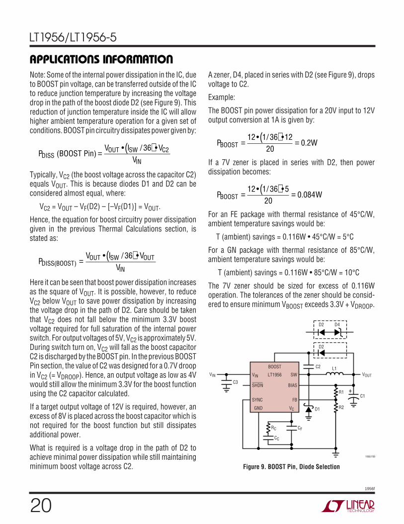
Note: Some of the internal power dissipation in the IC, dueto BOOST pin voltage, can be transferred outside of the ICto reduce junction temperature by increasing the voltagedrop in the path of the boost diode D2 (see Figure 9). Thisreduction of junction temperature inside the IC will allowhigher ambient temperature operation for a given set ofconditions. BOOST pin circuitry dissipates power given by:
PV I V
VDISSOUT SW C
IN (BOOST Pin) = ( )• / •36 2
Typically, VC2 (the boost voltage across the capacitor C2)equals VOUT. This is because diodes D1 and D2 can beconsidered almost equal, where:
VC2 = VOUT – VF(D2) – [–VF(D1)] = VOUT.
Hence, the equation for boost circuitry power dissipationgiven in the previous Thermal Calculations section, isstated as:
PV I V
VDISS BOOSTOUT SW OUT
IN( )
• / •= ( )36
Here it can be seen that boost power dissipation increasesas the square of VOUT. It is possible, however, to reduceVC2 below VOUT to save power dissipation by increasingthe voltage drop in the path of D2. Care should be takenthat VC2 does not fall below the minimum 3.3V boostvoltage required for full saturation of the internal powerswitch. For output voltages of 5V, VC2 is approximately 5V.During switch turn on, VC2 will fall as the boost capacitorC2 is discharged by the BOOST pin. In the previous BOOSTPin section, the value of C2 was designed for a 0.7V droopin VC2 (= VDROOP). Hence, an output voltage as low as 4Vwould still allow the minimum 3.3V for the boost functionusing the C2 capacitor calculated.
If a target output voltage of 12V is required, however, anexcess of 8V is placed across the boost capacitor which isnot required for the boost function but still dissipatesadditional power.
What is required is a voltage drop in the path of D2 toachieve minimal power dissipation while still maintainingminimum boost voltage across C2.
A zener, D4, placed in series with D2 (see Figure 9), dropsvoltage to C2.
Example:
The BOOST pin power dissipation for a 20V input to 12Voutput conversion at 1A is given by:
P WBOOST = ( ) =12 1 36 12
200 2
• / •.
If a 7V zener is placed in series with D2, then powerdissipation becomes:
P WBOOST = ( ) =12 1 36 5
200 084
• / •.
For an FE package with thermal resistance of 45°C/W,ambient temperature savings would be:
T (ambient) savings = 0.116W • 45°C/W = 5°C
For a GN package with thermal resistance of 85°C/W,ambient temperature savings would be:
T (ambient) savings = 0.116W • 85°C/W = 10°C
The 7V zener should be sized for excess of 0.116Woperation. The tolerances of the zener should be consid-ered to ensure minimum VBOOST exceeds 3.3V + VDROOP.
BOOST
VIN
D1
R1
VOUT
CF
CC
LT1956
SHDN
SYNC
SW
BIAS
FB
VCGND
C2
C1
L1
D2
RC
R2
1956 F09
C3
VIN
D2 D4
+
Figure 9. BOOST Pin, Diode Selection

21
LT1956/LT1956-5
1956f
APPLICATIO S I FOR ATIO
WU UU
Input Voltage vs Operating Frequency Considerations
The absolute maximum input supply voltage for the LT1956is specified at 60V. This is based on internal semiconduc-tor junction breakdown effects. The practical maximuminput supply voltage for the LT1956 may be less than 60Vdue to internal power dissipation or switch minimum ontime considerations.
For the extreme case of an output short-circuit fault toground, see the section Short-Circuit Considerations.
A detailed theoretical basis for estimating internal powerdissipation is given in the Thermal Calculations section.This will allow a first pass check of whether an application’smaximum input voltage requirement is suitable for theLT1956. Be aware that these calculations are for DC inputvoltages and that input voltage transients as high as 60Vare possible if the resulting increase in internal powerdissipation is of insufficient time duration to raise dietemperature significantly. For the FE package, this meanshigh voltage transients on the order of hundreds of milli-seconds are possible. If LT1956 (FE package) thermalcalculations show power dissipation is not suitable for thegiven application, the LT1766 (FE package) is a recom-mended alternative since it is identical to the LT1956 butruns cooler at 200kHz.
Switch minimum on time is the other factor that may limitthe maximum operational input voltage for the LT1956 ifpulse-skipping behavior is not allowed. For the LT1956,pulse-skipping may occur for VIN/(VOUT + VF) ratios > 4.(VF = Schottky diode D1 forward voltage drop, Figure 5.)If the LT1766 is used, the ratio increases to 10. Pulse-skipping is the regulator’s way of missing switch pulses tomaintain output voltage regulation. Although an increasein output ripple voltage can occur during pulse-skipping,a ceramic output capacitor can be used to keep ripplevoltage to a minimum (see output ripple voltage compari-son for tantalum vs ceramic output capacitors, Figure 3).
FREQUENCY COMPENSATION
Before starting on the theoretical analysis of frequencyresponse, the following should be remembered—the worsethe board layout, the more difficult the circuit will be tostabilize. This is true of almost all high frequency analog
circuits, read the Layout Considerations section first.Common layout errors that appear as stability problemsare distant placement of input decoupling capacitor and/or catch diode, and connecting the VC compensation to aground track carrying significant switch current. In addi-tion, the theoretical analysis considers only first ordernon-ideal component behavior. For these reasons, it isimportant that a final stability check is made with produc-tion layout and components.
The LT1956 uses current mode control. This alleviatesmany of the phase shift problems associated with theinductor. The basic regulator loop is shown in Figure 10.The LT1956 can be considered as two gm blocks, the erroramplifier and the power stage.
Figure 11 shows the overall loop response. At the VC pin,the frequency compensation components used are:RC = 2.2k, CC = 0.022µF and CF = 220pF. The outputcapacitor used is a 100µF, 10V tantalum capacitor withtypical ESR of 100mΩ.
The ESR of the tantalum output capacitor provides a usefulzero in the loop frequency response for maintaining stabil-ity. This ESR, however, contributes significantly to theripple voltage at the output (see Output Ripple Voltage inthe Applications Information section). It is possible toreduce capacitor size and output ripple voltage by replac-ing the tantalum output capacitor with a ceramic outputcapacitor because of its very low ESR. The zero providedby the tantalum output capacitor must now be reinsertedback into the loop. Alternatively, there may be caseswhere, even with the tantalum output capacitor, an addi-tional zero is required in the loop to increase phase marginfor improved transient response.
A zero can be added into the loop by placing a resistor (RC)at the VC pin in series with the compensation capacitor, CC,or by placing a capacitor (CFB) between the output and theFB pin.
When using RC, the maximum value has two limitations.First, the combination of output capacitor ESR and RC maystop the loop rolling off altogether. Second, if the loop gainis not rolled off sufficiently at the switching frequency,output ripple will perturb the VC pin enough to causeunstable duty cycle switching similar to subharmonic

22
LT1956/LT1956-5
1956f
APPLICATIO S I FOR ATIO
WU UU
oscillations. If needed, an additional capacitor (CF) can beadded across the RC/CC network from the VC pin to groundto further suppress VC ripple voltage.
With a tantalum output capacitor, the LT1956 alreadyincludes a resistor (RC) and filter capacitor (CF) at the VCpin (see Figures 10 and 11) to compensate the loop overthe entire VIN range (to allow for stable pulse skipping forhigh VIN-to-VOUT ratios ≥ 4). A ceramic output capacitorcan still be used with a simple adjustment to the resistorRC for stable operation (see Ceramic Capacitors sectionfor stabilizing LT1956). If additional phase margin isrequired, a capacitor (CFB) can be inserted between theoutput and FB pin but care must be taken for high outputvoltage applications. Sudden shorts to the output cancreate unacceptably large negative transients on the FBpin.
For VIN-to-VOUT ratios < 4, higher loop bandwidths arepossible by readjusting the frequency compensation com-ponents at the VC pin.
When checking loop stability, the circuit should be oper-ated over the application’s full voltage, current and tem-perature range. Proper loop compensation may be obtainedby empirical methods as described in Application Notes 19and 76.
CONVERTER WITH BACKUP OUTPUT REGULATOR
In systems with a primary and backup supply, for ex-ample, a battery powered device with a wall adapter input,the output of the LT1956 can be held up by the backupsupply with the LT1956 input disconnected. In this condi-tion, the SW pin will source current into the VIN pin. If theSHDN pin is held at ground, only the shut down current of25µA will be pulled via the SW pin from the second supply.With the SHDN pin floating, the LT1956 will consume itsquiescent operating current of 1.5mA. The VIN pin will alsosource current to any other components connected to theinput line. If this load is greater than 10mA or the inputcould be shorted to ground, a series Schottky diode mustbe added, as shown in Figure 12. With these safeguards,the output can be held at voltages up to the VIN absolutemaximum rating.
BUCK CONVERTER WITH ADJUSTABLE SOFT-START
Large capacitive loads or high input voltages can causehigh input currents at start-up. Figure 13 shows a circuitthat limits the dv/dt of the output at start-up, controllingthe capacitor charge rate. The buck converter is a typicalconfiguration with the addition of R3, R4, CSS and Q1.As the output starts to rise, Q1 turns on, regulating switch
FREQUENCY (Hz)
GAIN
(dB)
80
60
40
20
0
–20
–40
PHASE (DEG)
180
150
120
90
60
30
0
1956 F11
GAIN
PHASE
10
VIN = 12VVOUT = 5VILOAD = 500mACOUT = 100µF, 10V, 0.1Ω
1k 10k 1M100 100k
RC = 2.2kCC = 22nFCF = 220pF
–
+
1.22V
SW
VC
LT1956
GND
1956 F10
R1
OUTPUT
ESR
CF
CC
RC
RO200k
ERRORAMPLIFIER
FB
R2
C1
RLOAD
CURRENT MODEPOWER STAGE
gm = 2mho
gm =2000µmho
+
TANTALUM
ESL
C1
CERAMIC
CFB
Figure 10. Model for Loop Response Figure 11. Overall Loop Response

23
LT1956/LT1956-5
1956f
APPLICATIO S I FOR ATIO
WU UU
current via the VC pin to maintain a constant dv/dt at theoutput. Output rise time is controlled by the currentthrough CSS defined by R4 and Q1’s VBE. Once the outputis in regulation, Q1 turns off and the circuit operatesnormally. R3 is transient protection for the base of Q1.
RiseTimeR C V
V
SS OUT
BE=
( )( )( )4
Using the values shown in Figure 10,
Rise Time ms=( )( )( )
=47 10 15 10 5
0 75
3 9• •
.
–
The ramp is linear and rise times in the order of 100ms arepossible. Since the circuit is voltage controlled, the ramprate is unaffected by load characteristics and maximumoutput current is unchanged. Variants of this circuit can beused for sequencing multiple regulator outputs.
DUAL POLARITY OUTPUT CONVERTER
The circuit in Figure 14a generates both positive andnegative 5V outputs with all components under 3mmheight. The topology for the 5V output is a standard buckconverter. The –5V output uses a second inductor L2,diode D3 and output capacitor C6. The capacitor C4
5V, 1A
REMOVABLEINPUT
C20.1µF
CF220pF
RC2.2k
R354k
D110MQ060N
1956 F12
C32.2µF
D310MQ060N
MMSD914TI
L118µH
CC0.022µF
C1100µF10V
ALTERNATESUPPLY
R425k
R115.4k
R24.99k
BOOST
VIN LT1956
SHDN
SYNC
SW
BIAS
FB
VCGND+
Figure 12. Dual Source Supply with 25µA Reverse Leakage
OUTPUT5V1A
INPUT12V
1766 F13
C20.1µF
C1100µF
CSS15nF
D1C32.2µFCERAMIC
D2MMSD914TI
L118µH
R115.4k
R32k
R24.99k
R447k
Q1RC2.2k
CF220pF
CC0.022µF
BOOST BIAS
VIN
LT1956
SHDN
SYNC
SW
FB
VCGND
+
Figure 13. Buck Converter with Adjustable Soft-Start

24
LT1956/LT1956-5
1956f
couples energy to L2 and ensures equal voltages acrossL2 and L1 during steady state. Instead of using a trans-former for L1 and L2, uncoupled inductors were usedbecause they require less height than a single transformer,can be placed separately in the circuit layout for optimizedspace savings and reduce overall cost. This is true evenwhen the uncoupled inductors are sized (twice the value ofinductance of the transformer) in order to keep ripplecurrent comparable to the transformer solution. If a single
transformer becomes available to provide a better height/cost solution, refer to the dual output SEPIC circuit de-scription in Design Note 100 for correct transformerconnection.
During switch on-time, in steady state, the voltage acrossboth L1 and L2 is positive and equal; with energy (andcurrent) ramping up in each inductor. The current in L2 isprovided by the coupling capacitor C4. During switch off-time, current ramps downward in each inductor. The
APPLICATIO S I FOR ATIO
WU UU
VOUT1**5V
VOUT2**†
–5V
*SUMIDA CDRH4D28-150**SEE FIGURE 14c FOR VOUT1, VOUT2 LOAD CURRENT RELATIONSHIP † IF LOAD CAN GO TO ZERO, AN OPTIONAL PRELOAD OF 500Ω CAN BE USED TO IMPROVE REGULATION
VIN9V TO 12V
(TRANSIENTSTO 36V)
GND
1956 F14a
C20.1µF
CF220pF
RC2.2k
D1B0540W
C510µF6.3VCER
C610µF
6.3V CER
C32.2µF50V
CERAMIC
C410µF6.3VCER
D2MMSD914TI
D3B0540W
L1*15µH
L2*
CC3300pF
R115.4k
R24.99k
+
+
+
BOOST
VINLT1956
SHDN
SYNC
SW
FB
VCGND
Figure 14a. Dual Polarity Output Converter
VOUT1 LOAD CURRENT (mA)0
0
V OUT
2 M
AXIM
UM L
OAD
CURR
ENT
(mA)
50
150
200
250
500
350
200 400
1956 F15b
100
400
450
300
600 800
Figure 14b. VOUT2 (–5V) MaximumAllowable Load Current vs VOUT1(5V) Load Current
VOUT2 LOAD CURRENT (mA)0
4.75
|VOU
T2| (
V)
4.85
4.95
5.05
5.15
100 200 300 400
1956 F14c
500 600
5.25
4.80
4.90
5.00
5.10
5.20
5.30
VOUT1 LOAD CURRENT750mA
VOUT1 LOAD CURRENT250mA
VOUT1 LOAD CURRENT500mA
VOUT2 LOAD CURRENT (mA)0
EFFI
CIEN
CY (%
)
60
80
100
400
1956 F14d
40
20
50
70
90
30
10
0100 200 300 500
VOUT1 LOAD CURRENT750mA
VOUT1 LOAD CURRENT250mA
Figure 14c. VOUT2 (–5V) OutputVoltage vs Load Current
Figure 14d. Dual Polarity OutputConverter Efficiency

25
LT1956/LT1956-5
1956f
current in L2 and C4 flows via the catch diode D3, chargingthe negative output capacitor C6. If the negative output isnot loaded enough, it can go severely unregulated (be-come more negative). Figure 14b shows the maximumallowable –5V output load current (vs load current on the5V output) that will maintain the –5V output within 3%tolerance. Figure 14c shows the –5V output voltage regu-lation vs its own load current when plotted for threeseparate load currents on the 5V output. The efficiency ofthe dual output converter circuit shown in Figure 14a isgiven in Figure 14d.
POSITIVE-TO-NEGATIVE CONVERTER
The circuit in Figure 15 is a positive-to-negative topologyusing a grounded inductor. It differs from the standardapproach in the way the IC chip derives its feedback signalbecause the LT1956 accepts only positive feedback sig-nals. The ground pin must be tied to the regulated negativeoutput. A resistor divider to the FB pin, then provides theproper feedback voltage for the chip.
The following equation can be used to calculate maximumload current for the positive-to-negative converter:
APPLICATIO S I FOR ATIO
WU UU
II
V VV V f L
V V
V V V VMAX
PIN OUT
OUT INOUT IN
OUT IN OUT F=
+
+ +
–( )( )
( )( )( )( )( – . )
( – . )( )2
0 3
0 3
IP = maximum rated switch currentVIN = minimum input voltageVOUT = output voltageVF = catch diode forward voltage0.3 = switch voltage drop at 1.5A
Example: with VIN(MIN) = 5.5V, VOUT = 12V, L = 15µH,VF = 0.63V, IP = 1.5A: IMAX = 0.36A.
INDUCTOR VALUE
The criteria for choosing the inductor is typically based onensuring that peak switch current rating is not exceeded.This gives the lowest value of inductance that can be used,but in some cases (lower output load currents) it may givea value that creates unnecessarily high output ripplevoltage.
The difficulty in calculating the minimum inductor sizeneeded is that you must first decide whether the switcherwill be in continuous or discontinuous mode at the criticalpoint where switch current reaches 1.5A. The first step isto use the following formula to calculate the load currentabove which the switcher must use continuous mode. Ifyour load current is less than this, use the discontinuousmode formula to calculate minimum inductor needed. Ifload current is higher, use the continuous mode formula.
Output current where continuous mode is needed:
IV I
V V V V VCONTIN P
IN OUT IN OUT F>
+ + +( ) ( )
( )( )
2 2
4
Minimum inductor discontinuous mode:
LV I
f IMIN
OUT OUT
P= 2
2( )( )
( )( )
OUTPUT**–12V, 0.25A
VIN12V
1956 F15
C20.1µF
CC
RC
D110MQO60N
R136.5k
C1100µF20V TANT
C32.2µF
25V
D2MMSD914TI
L1*7µH
CF
BOOST
LT1956
VIN SW
FBGND VC
R24.12k
* INCREASE L1 TO 10µH OR 18µH FOR HIGHER CURRENT APPLICATIONS. SEE APPLICATIONS INFORMATION
** MAXIMUM LOAD CURRENT DEPENDS ON MINIMUM INPUT VOLTAGE AND INDUCTOR SIZE. SEE APPLICATIONS INFORMATION
+
Figure 15. Positive-to-Negative Converter

26
LT1956/LT1956-5
1956f
U
PACKAGE DESCRIPTIOMinimum inductor continuous mode:
L
V V
f V V I IV V
V
MININ OUT
IN OUT P OUTOUT F
IN
=+ + +
( )( )
( )( ) –( )
2 1
For a 12V to –12V converter using the LT1956 with peakswitch current of 1.5A and a catch diode of 0.63V:
I ACONT >+ + +
=( ) ( . )( )( . )
.12 1 5
4 12 12 12 12 0 630 370
2 2
For a load current of 0.25A, this says that discontinuousmode can be used and the minimum inductor needed isfound from:
L HMIN = = µ2 12 0 25500 10 1 5
5 33 2( )( . )
( • )( . ).
In practice, the inductor should be increased by about30% over the calculated minimum to handle losses andvariations in value. This suggests a minimum inductor of7µH for this application.
Ripple Current in the Input and Output Capacitors
Positive-to-negative converters have high ripple currentin the input capacitor. For long capacitor lifetime, theRMS value of this current must be less than the highfrequency ripple current rating of the capacitor. Thefollowing formula will give an approximate value for RMSripple current. This formula assumes continuous modeand large inductor value. Small inductors will give some-what higher ripple current, especially in discontinuousmode. The exact formulas are very complex and appearin Application Note 44, pages 29 and 30. For our pur-poses here I have simply added a fudge factor (ff). Thevalue for ff is about 1.2 for higher load currents and L≥15µH. It increases to about 2.0 for smaller inductors atlower load currents.
Capacitor I ff IVVRMS OUTOUT
IN= ( )( )
ff = 1.2 to 2.0
The output capacitor ripple current for the positive-to-negative converter is similar to that for a typical buckregulator—it is a triangular waveform with peak-to-peakvalue equal to the peak-to-peak triangular waveform of theinductor. The low output ripple design in Figure 14 placesthe input capacitor between VIN and the regulated negativeoutput. This placement of the input capacitor significantlyreduces the size required for the output capacitor (versusplacing the input capacitor between VIN and ground).
The peak-to-peak ripple current in both the inductor andoutput capacitor (assuming continuous mode) is:
IP-P
P-P
=
= = ++ +
=
DC Vf L
DC Duty CycleV V
V V V
I RMSI
IN
OUT F
OUT IN F
COUT
••
( )12
The output ripple voltage for this configuration is as low asthe typical buck regulator based predominantly on theinductor’s triangular peak-to-peak ripple current and theESR of the chosen capacitor (see Output Ripple Voltage inApplications Information).
Diode Current
Average diode current is equal to load current. Peak diodecurrent will be considerably higher.
Peak diode current:
Continuous Mode
IV V
VV V
L f V V
Discontinuous ModeI V
L f
OUTIN OUT
IN
IN OUT
IN OUT
OUT OUT
=+ +
+
=
( ) ( )( )( )( )( )
( )( )( )( )
2
2
Keep in mind that during start-up and output overloads,average diode current may be much higher than withnormal loads. Care should be used if diodes rated less than1A are used, especially if continuous overload conditionsmust be tolerated.

27
LT1956/LT1956-5
1956f
U
PACKAGE DESCRIPTIO
Information furnished by Linear Technology Corporation is believed to be accurate and reliable.However, no responsibility is assumed for its use. Linear Technology Corporation makes no represen-tation that the interconnection of its circuits as described herein will not infringe on existing patent rights.
FE Package16-Lead Plastic TSSOP (4.4mm)(Reference LTC DWG # 05-08-1663)
Exposed Pad Variation BB
FE16 (BB) TSSOP 0203
0.09 – 0.20(.0036 – .0079)
0° – 8°
0.45 – 0.75(.018 – .030)
4.30 – 4.50*(.169 – .177)
6.40BSC
1 3 4 5 6 7 8
10 9
4.90 – 5.10*(.193 – .201)
16 1514 13 12 11
1.10(.0433)
MAX
0.05 – 0.15(.002 – .006)
0.65(.0256)
BSC
2.94(.116)
0.195 – 0.30(.0077 – .0118)
2RECOMMENDED SOLDER PAD LAYOUT
0.45 ±0.05
0.65 BSC
4.50 ±0.10
6.60 ±0.10
1.05 ±0.10
2.94(.116)
3.58(.141)
3.58(.141)
MILLIMETERS(INCHES) *DIMENSIONS DO NOT INCLUDE MOLD FLASH. MOLD FLASH
SHALL NOT EXCEED 0.150mm (.006") PER SIDE
NOTE:1. CONTROLLING DIMENSION: MILLIMETERS
2. DIMENSIONS ARE IN
3. DRAWING NOT TO SCALE
SEE NOTE 4
4. RECOMMENDED MINIMUM PCB METAL SIZE FOR EXPOSED PAD ATTACHMENT

28
LT1956/LT1956-5
1956f
LT/TP 0303 2K • PRINTED IN USA
LINEAR TECHNOLOGY CORPORATION 2001
RELATED PARTSPART NUMBER DESCRIPTION COMMENTSLT1074/LT1076/ Step-Down Switching Regulators Up to 64V Input, 100kHz, 5A and 2ALT1076HVLT1082 1A High Voltage/Efficiency Switching Voltage Regulator Up to 75V Input, 60kHz OperationLT1370 High Efficiency DC/DC Converter Up to 42V, 6A, 500kHz SwitchLT1371 High Efficiency DC/DC Converter Up to 35V, 3A, 500kHz SwitchLT1375/LT1376 1.5A, 500kHz Step-Down Switching Regulators Operation Up to 25V Input, Synchronizable (LT1375),
N8, S8, S16LT1616 600mA, 1.4MHz Step-Down Switching Regulator 3.6V to 25V VIN, 6-Lead ThinSOTTM
LT1676 Wide Input Range, High Efficiency, Step-Down Switching Regulator 7.4V to 60V VIN, 100kHz Operation, 700mA Internal Switch, S8LT1765 Monolithic 3A, 1.25MHz Step-Down Regulator VIN: 3V to 25V; VREF = 1.2V; S8, TSSOP-16E
Exposed PadLT1766 Wide Input Range, High Efficiency, Step-Down Switching Regulator 5.5V to 60V Input, 200kHz Operation, 1.5A Internal Switch,
TSSOP-16ELT1767 Monolithic 1.5A, 1.25MHz Step-Down Regulator VIN: 3V to 25V; VREF = 1.2V; MS8LT1776 Wide Input Range, High Efficiency, Step-Down Switching Regulator Up to 7.4V to 60V, 200kHz Operation, 700mA Internal Switch,
TSSOP-16ELT1777 Low Noise Buck Regulator Operation Up to 48V, Controlled Voltage
and Current Slew Rates, S16ThinSOT is a trademark of Linear Technology Corporation.
Linear Technology Corporation1630 McCarthy Blvd., Milpitas, CA 95035-7417(408) 432-1900 FAX: (408) 434-0507 www.linear.com
GN Package16-Lead Plastic SSOP (Narrow .150 Inch)
(Reference LTC DWG # 05-08-1641)
GN16 (SSOP) 0502
1 2 3 4 5 6 7 8
.229 – .244(5.817 – 6.198)
.150 – .157**(3.810 – 3.988)
16 15 14 13
.189 – .196*(4.801 – 4.978)
12 11 10 9
.016 – .050(0.406 – 1.270)
.015 ± .004(0.38 ± 0.10)
× 45°
0° – 8° TYP.007 – .0098(0.178 – 0.249)
.053 – .068(1.351 – 1.727)
.008 – .012(0.203 – 0.305)
.004 – .0098(0.102 – 0.249)
.0250(0.635)
BSC
.009(0.229)
REF
.254 MIN
RECOMMENDED SOLDER PAD LAYOUT
.150 – .165
.0250 TYP.0165 ± .0015
.045 ±.005
*DIMENSION DOES NOT INCLUDE MOLD FLASH. MOLD FLASH SHALL NOT EXCEED 0.006" (0.152mm) PER SIDE**DIMENSION DOES NOT INCLUDE INTERLEAD FLASH. INTERLEAD FLASH SHALL NOT EXCEED 0.010" (0.254mm) PER SIDE
INCHES(MILLIMETERS)
NOTE:1. CONTROLLING DIMENSION: INCHES
2. DIMENSIONS ARE IN
3. DRAWING NOT TO SCALE
U
PACKAGE DESCRIPTIO