
Family Reference Manual p17 - UART
42
© 2008 Microchip Technology Inc. DS70188C-page 17-1 U A R T 17 Section 17. UART HIGHLIGHTS This section of the manual contains the following major topics: 17.1 Introduction ............................................................ ........... ......... .................................. 17-2 17.2 Control Registers ......... ............................... .......... ......................................... ........... ... 17-3 17.3 UART Baud Rate Generator ......... ........... .............................. .......... .......................... 17-10 17.4 UART Configuration.................. .......... .............................. .......... .............................. . 17-12 17.5 UART Transmitter ............................... .......... ......................................... .......... ..........17-13 17.6 Data Bit Det ection ................... ........... .......... ......................................... .......... ........... 17-18 17.7 UART Receiver ................................................... .......... ............................................. 17-19 17.8 Using t he UART for 9-bit Communication ........................................ .......... ................ 17-23 17.9 Other Features of the UART ............................. .......... .................... ......... ........... ....... 17-25 17.10 UART Operation with DMA .............................................................................. ..........17-27 17.11 UART Operation During CPU Sleep and Idle Modes ........................... .......... ........... 17-30 17.12 Operation of UxCTS and UxRTS Control Pins ......... ......... ................... .......... ........... 17-31 17.13 Infrared Support ......................................................................................................... 17-33 17.14 LIN Support................. .......... ........... ......... ............................... .......... ........................ 17-36 17.15 Registers Map................... ........................................ ........... .................... .......... ........17-38 17.16 Design Tips .................... .......... ........... ................... ........... .......... .............................. . 17-39 17.17 Related Application Notes........... ............................ .......... ............................... ..........17-40 17.18 Revision History ......... ........... ..................................................................................... 17-41
-
Upload
raji-pillalamarri -
Category
Documents
-
view
227 -
download
0
Transcript of Family Reference Manual p17 - UART
8/2/2019 Family Reference Manual p17 - UART
http://slidepdf.com/reader/full/family-reference-manual-p17-uart 1/42
© 2008 Microchip Technology Inc. DS70188C-page 17-1
Section 17. UART
HIGHLIGHTS
This section of the manual contains the following major topics:
17.1 Introduction ..................................................................................................................17-2
17.2 Control Registers ......................................................................................................... 17-3
17.3 UART Baud Rate Generator ......................................................................................17-10
17.4 UART Configuration................................................................................................... 17-12
17.5 UART Transmitter ......................................................................................................17-13
17.6 Data Bit Detection ...................................................................................................... 17-18
17.7 UART Receiver .......................................................................................................... 17-19
17.8 Using the UART for 9-bit Communication..................................................................17-2317.9 Other Features of the UART ......................................................................................17-25
17.10 UART Operation with DMA ........................................................................................17-27
17.11 UART Operation During CPU Sleep and Idle Modes ................................................ 17-30
17.12 Operation of UxCTS and UxRTS Control Pins .......................................................... 17-31
17.13 Infrared Support ......................................................................................................... 17-33
17.14 LIN Support................................................................................................................ 17-36
17.15 Registers Map............................................................................................................17-38
17.16 Design Tips ................................................................................................................ 17-39
17.17 Related Application Notes..........................................................................................17-40
17.18 Revision History .........................................................................................................17-41

8/2/2019 Family Reference Manual p17 - UART
http://slidepdf.com/reader/full/family-reference-manual-p17-uart 2/42
dsPIC33F Family Reference Manual
DS70188C-page 17-2 © 2008 Microchip Technology Inc.
17.1 INTRODUCTION
The Universal Asynchronous Receiver Transmitter (UART) module is one of the serial I/O
modules available in the dsPIC33F device family. The UART is a full-duplex, asynchronous
communication channel that communicates with peripheral devices and personal computers
using protocols, such as RS-232, RS-485, LIN, and IrDA ® . The module also supports the
hardware flow control option with UxCTS and UxRTS pins and includes the IrDA encoder and
decoder.
The primary features of the UART module are as follows:
• Full-Duplex, 8-bit or 9-bit Data Transmission through the UxTX and UxRX pins
• Even, Odd or No Parity options (for 8-bit data)
• One or two Stop bits
• Hardware Auto-Baud feature
• Hardware Flow Control option with UxCTS and UxRTS pins
• Fully Integrated Baud Rate Generator with 16-bit Prescaler
• Baud Rates ranging from 10 Mbps to 38 bps at 40 MIPS
• 4-deep First-In-First-Out (FIFO) Transmit Data Buffer
• 4-deep FIFO Receive Data Buffer
• Parity, Framing, and Buffer Overrun Error Detection
• Support for 9-bit mode with Address Detect (9th bit = 1)• Transmit and Receive Interrupts
• Loopback mode for Diagnostic Support
• IrDA Encoder and Decoder Logic
• LIN Bus Support
• 16x Baud Clock Output for External IrDA Encoder/Decoder support
A simplified block diagram of the UART is shown in Figure 17-1. The UART module consists of
the following key hardware elements:
• Baud Rate Generator
• Asynchronous Transmitter
• Asynchronous Receiver
Figure 17-1: UART Simplified Block Diagram
Note: Each dsPIC33F family device variant may have one or more UART modules. An ‘x’
used in the names of pins, control/status bits and registers denotes the particular
UART module number. Refer to the specific device data sheets for more details.
Baud Rate Generator
UxRX
Hardware Flow Control
UARTx Receiver
UARTx Transmitter UxTX
UxCTS
UxRTS
BCLKxIrDA ®

8/2/2019 Family Reference Manual p17 - UART
http://slidepdf.com/reader/full/family-reference-manual-p17-uart 3/42
© 2008 Microchip Technology Inc. DS70188C-page 17-3
Section 17. UART
17.2 CONTROL REGISTERS
This section outlines the specific functions of each register that controls the operation of the
UART module:
• UxMODE: UARTx Mode Register
- Enables or disables the UART module
- Enables or disables the IrDA encoder and decoder
- Enables or disables the WAKE, ABAUD, and Loopback features- Enables or disables the UxRTS and UxCTS pins
- Configures the UxRTS pin for the desired mode of operation
- Configures the polarity of the UxRx pin
- Selects the type of baud rate
- Selects the number of data bits, parity, and stop bits
• UxSTA: UARTx Status and Control Register
- Selects the Transmission Interrupt mode
- Selects the Receive Interrupt mode
- Enables or disables the UART transmission
- Controls the Address Detect mode
- Indicates various status conditions, such as transmit and receive buffer state, parity
error, framing error, and overflow error• UxRXREG: UARTx Receive Register
- Stores the received data
• UxTXREG: UARTx Transmit Register (Write-Only)
- Provides the data to be transmitted
• UxBRG: UARTx Baud Rate Register
- Stores the baud rate value of the transmitted or received data
8/2/2019 Family Reference Manual p17 - UART
http://slidepdf.com/reader/full/family-reference-manual-p17-uart 4/42
dsPIC33F Family Reference Manual
DS70188C-page 17-4 © 2008 Microchip Technology Inc.
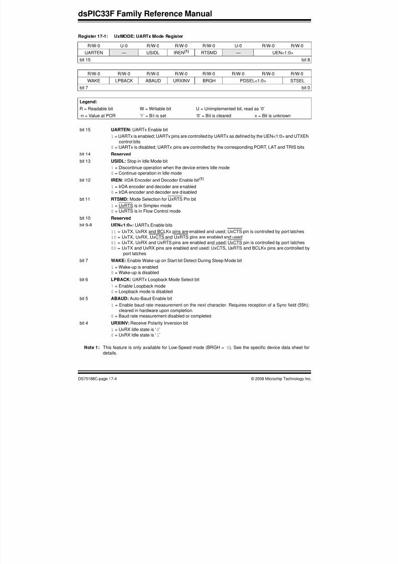
Register 17-1: UxMODE: UARTx Mode Register
R/W-0 U-0 R/W-0 R/W-0 R/W-0 U-0 R/W-0 R/W-0
UARTEN — USIDL IREN(1) RTSMD — UEN<1:0>
bit 15 bit 8
R/W-0 R/W-0 R/W-0 R/W-0 R/W-0 R/W-0 R/W-0 R/W-0WAKE LPBACK ABAUD URXINV BRGH PDSEL<1:0> STSEL
bit 7 bit 0
Legend:
R = Readable bit W = Writable bit U = Unimplemented bit, read as ‘0’
-n = Value at POR ‘1’ = Bit is set ‘0’ = Bit is cleared x = Bit is unknown
bit 15 UARTEN: UARTx Enable bit
1 = UARTx is enabled; UARTx pins are controlled by UARTx as defined by the UEN<1:0> and UTXEN
control bits
0 = UARTx is disabled; UARTx pins are controlled by the corresponding PORT, LAT and TRIS bits
bit 14 Reserved
bit 13 USIDL: Stop in Idle Mode bit
1 = Discontinue operation when the device enters Idle mode
0 = Continue operation in Idle mode
bit 12 IREN: IrDA Encoder and Decoder Enable bit(1)
1 = IrDA encoder and decoder are enabled
0 = IrDA encoder and decoder are disabled
bit 11 RTSMD: Mode Selection for UxRTS Pin bit
1 = UxRTS is in Simplex mode
0 = UxRTS is in Flow Control mode
bit 10 Reserved
bit 9-8 UEN<1:0>: UARTx Enable bits
11 = UxTX, UxRX and BCLKx pins are enabled and used; UxCTS pin is controlled by port latches
10 = UxTX, UxRX, UxCTS and UxRTS pins are enabled and used
01 = UxTX, UxRX and UxRTS pins are enabled and used; UxCTS pin is controlled by port latches
00 = UxTX and UxRX pins are enabled and used; UxCTS, UxRTS and BCLKx pins are controlled by
port latches
bit 7 WAKE: Enable Wake-up on Start bit Detect During Sleep Mode bit
1 = Wake-up is enabled
0 = Wake-up is disabled
bit 6 LPBACK: UARTx Loopback Mode Select bit
1 = Enable Loopback mode
0 = Loopback mode is disabled
bit 5 ABAUD: Auto-Baud Enable bit
1 = Enable baud rate measurement on the next character. Requires reception of a Sync field (55h);cleared in hardware upon completion.
0 = Baud rate measurement disabled or completed
bit 4 URXINV: Receive Polarity Inversion bit
1 = UxRX Idle state is ‘0’
0 = UxRX Idle state is ‘1’
Note 1: This feature is only available for Low-Speed mode (BRGH = 0). See the specific device data sheet for
details.

8/2/2019 Family Reference Manual p17 - UART
http://slidepdf.com/reader/full/family-reference-manual-p17-uart 5/42
© 2008 Microchip Technology Inc. DS70188C-page 17-5
Section 17. UART
bit 3 BRGH: High Baud Rate Select bit
1 = High speed
0 = Low speed
bit 2-1 PDSEL<1:0>: Parity and Data Selection bits
11 = 9-bit data, no parity
10 = 8-bit data, odd parity
01 = 8-bit data, even parity
00 = 8-bit data, no parity
bit 0 STSEL: Stop Selection bit
1 = 2 Stop bits
0 = 1 Stop bit
Register 17-1: UxMODE: UARTx Mode Register (Continued)
Note 1: This feature is only available for Low-Speed mode (BRGH = 0). See the specific device data sheet for
details.

8/2/2019 Family Reference Manual p17 - UART
http://slidepdf.com/reader/full/family-reference-manual-p17-uart 6/42
dsPIC33F Family Reference Manual
DS70188C-page 17-6 © 2008 Microchip Technology Inc.
Register 17-2: UxSTA: UARTx Status and Control Register
R/W-0 R/W-0 R/W-0 U-0 R/W-0 R/W-0 R-0 R-1
UTXISEL1 UTXINV UTXISEL0 — UTXBRK UTXEN UTXBF TRMT
bit 15 bit 8
R/W-0 R/W-0 R/W-0 R-1 R-0 R-0 R/C-0 R-0URXISEL<1:0> ADDEN RIDLE PERR FERR OERR URXDA
bit 7 bit 0
Legend: C = Clearable bit
R = Readable bit W = Writable bit U = Unimplemented bit, read as ‘0’
-n = Value at POR ‘1’ = Bit is set ‘0’ = Bit is cleared x = Bit is unknown
bit 15,13 UTXISEL<1:0> Transmission Interrupt Mode Selection bits
11 = Reserved
10 = Interrupt generated when a character is transferred to the Transmit Shift register and the
transmit buffer becomes empty
01 = Interrupt generated when the last transmission is over (i.e., the last character has been shiftedout of the Transmit Shift register) and all the transmit operations are completed
00 = Interrupt generated when any character is transferred to the Transmit Shift Register (which
implies at least one location is empty in the transmit buffer)
bit 14 UTXINV: Transmit Polarity Inversion bit
1 = UxTX Idle state is ‘1’
0 = UxTX Idle state is ‘0’
bit 12 Unimplemented: Read as ‘0’
bit 11 UTXBRK: Transmit Break bit
1 = UxTX pin is driven low regardless of the transmitter state (Sync Break transmission – Start bit
followed by twelve ‘0’s and a Stop bit)
0 = Sync Break transmission is disabled or completed
bit 10 UTXEN: Transmit Enable bit1 = UARTx transmitter enabled; UxTX pin is controlled by UARTx (if UARTEN = 1)
0 = UARTx transmitter disabled; any pending transmission is aborted and the buffer is reset; UxTX pin
is controlled by PORT
bit 9 UTXBF: Transmit Buffer Full Status bit (read-only)
1 = Transmit buffer is full
0 = Transmit buffer is not full; at least one more data word can be written
bit 8 TRMT: Transmit Shift Register is Empty bit (read-only)
1 = Transmit Shift register is empty and the transmit buffer is empty (i.e., the last transmission has
completed)
0 = Transmit Shift register is not empty; a transmission is in progress or queued in the transmit buffer
bit 7-6 URXISEL<1:0>: Receive Interrupt Mode Selection bits
11 = Interrupt flag bit is set when the receive buffer is full (i.e., has 4 data characters)
10 = Interrupt flag bit is set when the receive buffer is 3/4 full (i.e., has 3 data characters)0x = Interrupt flag bit is set when a character is received
bit 5 ADDEN: Address Character Detect bit (bit 8 of received data = 1)
1 = Address Detect mode enabled. If 9-bit mode is not selected, this control bit has no effect.
0 = Address Detect mode disabled
bit 4 RIDLE: Receiver Idle bit (read-only)
1 = Receiver is Idle
0 = Data is being received
8/2/2019 Family Reference Manual p17 - UART
http://slidepdf.com/reader/full/family-reference-manual-p17-uart 7/42
© 2008 Microchip Technology Inc. DS70188C-page 17-7
Section 17. UART
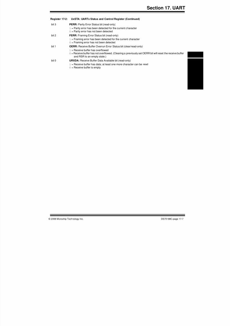
bit 3 PERR: Parity Error Status bit (read-only)
1 = Parity error has been detected for the current character
0 = Parity error has not been detected
bit 2 FERR: Framing Error Status bit (read-only)
1 = Framing error has been detected for the current character
0 = Framing error has not been detected
bit 1 OERR: Receive Buffer Overrun Error Status bit (clear/read-only)
1 = Receive buffer has overflowed
0 = Receive buffer has not overflowed. (Clearing a previously set OERR bit will reset the receive buffer
and RSR to an empty state.)
bit 0 URXDA: Receive Buffer Data Available bit (read-only)
1 = Receive buffer has data; at least one more character can be read
0 = Receive buffer is empty
Register 17-2: UxSTA: UARTx Status and Control Register (Continued)

8/2/2019 Family Reference Manual p17 - UART
http://slidepdf.com/reader/full/family-reference-manual-p17-uart 8/42
dsPIC33F Family Reference Manual
DS70188C-page 17-8 © 2008 Microchip Technology Inc.
Register 17-3: UxRXREG: UARTx Receive Register
U-0 U-0 U-0 U-0 U-0 U-0 U-0 R-0
— — — — — — — URX8
bit 15 bit 8
R-0 R-0 R-0 R-0 R-0 R-0 R-0 R-0URX<7:0>
bit 7 bit 0
Legend:
R = Readable bit W = Writable bit U = Unimplemented bit, read as ‘0’
-n = Value at POR ‘1’ = Bit is set ‘0’ = Bit is cleared x = Bit is unknown
bit 15-9 Unimplemented: Read as ‘0’
bit 8 URX8: Data bit 8 of the Received Character (in 9-bit mode)
bit 7-0 URX<7:0>: Data bits 7-0 of the Received Character
Register 17-4: UxTXREG: UARTx Transmit Register (Write-Only)
U-0 U-0 U-0 U-0 U-0 U-0 U-0 W-x
— — — — — — — UTX8
bit 15 bit 8
W-x W-x W-x W-x W-x W-x W-x W-x
UTX<7:0>
bit 7 bit 0
Legend:
R = Readable bit W = Writable bit U = Unimplemented bit, read as ‘0’
-n = Value at POR ‘1’ = Bit is set ‘0’ = Bit is cleared x = Bit is unknown
bit 15-9 Unimplemented: Read as ‘0’
bit 8 UTX8: Data bit 8 of the Transmitted Character (in 9-bit mode)
bit 7-0 UTX<7:0>: Data bits 7-0 of the Transmitted Character
8/2/2019 Family Reference Manual p17 - UART
http://slidepdf.com/reader/full/family-reference-manual-p17-uart 9/42
© 2008 Microchip Technology Inc. DS70188C-page 17-9
Section 17. UART
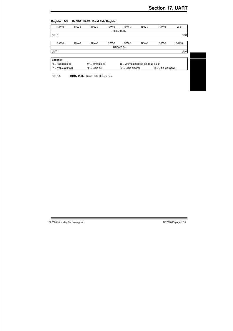
Register 17-5: UxBRG: UARTx Baud Rate Register
R/W-0 R/W-0 R/W-0 R/W-0 R/W-0 R/W-0 R/W-0 W-x
BRG<15:8>
bit 15 bit 8
R/W-0 R/W-0 R/W-0 R/W-0 R/W-0 R/W-0 R/W-0 R/W-0BRG<7:0>
bit 7 bit 0
Legend:
R = Readable bit W = Writable bit U = Unimplemented bit, read as ‘0’
-n = Value at POR ‘1’ = Bit is set ‘0’ = Bit is cleared x = Bit is unknown
bit 15-0 BRG<15:0>: Baud Rate Divisor bits

8/2/2019 Family Reference Manual p17 - UART
http://slidepdf.com/reader/full/family-reference-manual-p17-uart 10/42
dsPIC33F Family Reference Manual
DS70188C-page 17-10 © 2008 Microchip Technology Inc.
17.3 UART BAUD RATE GENERATOR
The UART module includes a dedicated 16-bit Baud Rate Generator (BRG). The UxBRG register
controls the period of a free-running, 16-bit timer. Equation 17-1 shows the formula for computing
the baud rate with BRGH = 0.
Equation 17-1: UART Baud Rate (BRGH = 0)
Example 17-1 shows the calculation of the baud rate error for the following conditions:
• FCY = 4 MHz
• Desired Baud Rate = 9600
Example 17-1: Baud Rate Error Calculation (BRGH = 0)
The maximum baud rate (BRGH = 0) possible is FCY /16 (for UxBRG = 0), and the minimum baud
rate possible is FCY /(16 * 65536).
Equation 17-2 shows the formula for computing the baud rate with BRGH = 1.
Note: F CY denotes the instruction cycle clock frequency (FOSC /2).
Baud RateF CY
16 UxBRG 1+( )×-----------------------------------------------=
UxBRGF
CY
16 Baud Rate×-------------------------------------- 1–=
......(1)
......(2)
Desired Baud RateF
CY
16 UxBRG 1+( )×-----------------------------------------------=
Solving for UxBRG value:
UxBRGF
CY Desired Baud Rate ⁄
16-------------------------------------------------------------- 1–=
Calculated Baud Rate4000000
16 25 1+( )×---------------------------------=
Error Calculated Baud Rate Desired Baud Rate–
Desired Baud Rate--------------------------------------------------------------------------------------------------------=
9615 9600–
9600------------------------------=
0.16%=
4000000 9600 ⁄ 16
---------------------------------------- 1–⎝ ⎠ ⎛ ⎞
=
25=
......(1)
......(2)
9615=

8/2/2019 Family Reference Manual p17 - UART
http://slidepdf.com/reader/full/family-reference-manual-p17-uart 11/42
© 2008 Microchip Technology Inc. DS70188C-page 17-11
Section 17. UART
Equation 17-2: UART Baud Rate (BRGH = 1)
The maximum baud rate (BRGH = 1) possible is FCY /4 (for UxBRG = 0), and the minimum baud
rate possible is FCY /(4 * 65536).
Writing a new value to the UxBRG register causes the BRG timer to be reset (cleared). This
ensures the BRG does not wait for a timer overflow before generating the new baud rate.
17.3.1 BCLKx Output
The BCLKx pin will output the 16x baud clock if the UART and BCLKx output are enabled
(UEN<1:0> = 11). This feature is used for external IrDA encoder/decoder support (refer to
Figure 17-2). BCLKx output stays high during Sleep mode. BCLKx is forced as an output as long
as the UART is kept in this mode (UEN<1:0> = 11), regardless of the PORTx and TRISx latch
bits.
Figure 17-2: BCLKx Output vs. UxBRG Programming
Note: F CY denotes the instruction cycle clock frequency.
Baud RateF
CY
4 UxBRG 1+( )×--------------------------------------------=
UxBRGF
CY
4 Baud Rate×----------------------------------- 1–=
......(1)
......(2)
(N + 1)Tcy
Tcy
BCLKx @ BRG = 0
BCLKx @ BRG = 1
BCLKx @ BRG = 2
BCLKx @ BRG = 3
BCLKx @ BRG = 4
BCLKx @ BRG = N
UxTX
8/2/2019 Family Reference Manual p17 - UART
http://slidepdf.com/reader/full/family-reference-manual-p17-uart 12/42
dsPIC33F Family Reference Manual
DS70188C-page 17-12 © 2008 Microchip Technology Inc.
17.4 UART CONFIGURATION
The UART uses standard Non-Return-to-Zero (NRZ) format (one Start bit, eight or nine data bits,
and one or two Stop bits). Parity is supported by the hardware and may be configured by the user
application as even, odd, or no parity. The most common data format is 8 bits, no parity, and one
Stop bit (denoted as 8, N, 1), which is the default (POR) setting. The number of data bits and Stop
bits and the parity are specified in the PDSEL<1:0> (UxMODE<2:1>) and STSEL (UxMODE<0>)
bits. An on-chip, dedicated, 16-bit Baud Rate Generator can be used to derive standard baud
rate frequencies from the oscillator. The UART transmits and receives the Least Significant bit(LSb) first. The UART module’s transmitter and receiver are functionally independent, but use
the same data format and baud rate.
17.4.1 Enabling the UART
The UART module is enabled by setting the UARTEN (UxMODE<15>) bit and UTXEN
(UxSTA<10>) bit. Once enabled, the UxTX and UxRX pins are configured as an output and an
input, respectively, overriding the TRIS and PORT register bit settings for the corresponding I/O
port pins. The UxTX pin is at logic ‘1’ when no transmission is taking place.
17.4.2 Disabling the UART
The UART module is disabled by clearing the UARTEN (UxMODE<15>) bit. This is the default
state after any Reset. If the UART is disabled, all UART pins operate as port pins under the
control of their corresponding PORT and TRIS bits.
Disabling the UART module resets the buffers to empty states. Any data characters in the buffers
are lost and the baud rate counter is reset.
All error and status flags associated with the UART module are reset when the module is
disabled. The URXDA, OERR, FERR, PERR, UTXEN, UTXBRK, and UTXBF bits are cleared,
whereas the RIDLE and TRMT bits are set. Other control bits (including ADDEN, URXISEL<1:0>
and UTXISEL<1:0>) and the UxMODE and UxBRG registers are not affected.
Clearing the UARTEN bit while the UART is active will abort all pending transmissions and
receptions, and reset the module as defined above. Re-enabling the UART will restart the UART
in the same configuration.
Note: The UTXEN bit should not be set until the UARTEN bit has been set; otherwise,
UART transmissions will not be enabled.

8/2/2019 Family Reference Manual p17 - UART
http://slidepdf.com/reader/full/family-reference-manual-p17-uart 13/42
© 2008 Microchip Technology Inc. DS70188C-page 17-13
Section 17. UART
17.5 UART TRANSMITTER
The UART transmitter block diagram is shown in Figure 17-3. The heart of the transmitter is the
Transmit Shift (UxTSR) register. The Shift register obtains its data from the transmit FIFO buffer,
UxTXREG. The UxTXREG register is loaded with data in software. The UxTSR register is not
loaded until the Stop bit has been transmitted from the previous load. As soon as the Stop bit is
transmitted, the UxTSR is loaded with new data from the UxTXREG register (if available).
Figure 17-3: UART Transmitter Block Diagram
Transmission is enabled by setting the UTXEN enable bit (UxSTA<10>). The actual transmission
will not occur until the UxTXREG register has been loaded with data and the Baud Rate
Generator (UxBRG) has produced a shift clock (Figure 17-3). Normally, when transmission is first
started, the UxTSR register is empty, so a transfer to the UxTXREG register will result in an
immediate transfer to UxTSR. Clearing the UTXEN bit during a transmission will cause the
transmission to be aborted and will reset the transmitter. As a result, the UxTX pin will revert toa high-impedance state.
In order to select 9-bit transmission, the PDSEL<1:0> bits (UxMODE<2:1>) should be set to ‘11’
and the ninth bit should be written to the UTX8 bit (UxTXREG<8>). A word write should be
performed to UxTXREG so that all nine bits are written at the same time.
Note: The UxTSR register is not mapped in data memory, so it is not available to the user
application.
Word Write-Only Word
UTX8 UxTXREG Low Byte
Load UxTSR
Transmit Control
– Control UxTSR
– Control Buffer
– Generate Flags
– Generate Interrupt
UxTXIF
Data
(Start)
(Stop)
Parity ParityGenerator
Transmit Shift Register (UxTSR)
÷ 16 Divider
ControlSignals
16x Baud Clockfrom Baud Rate
Generator
Internal Data Bus
UTXBRK
UxTX
Note: ‘x’ denotes the UART number.
UxTX
UxMODE UxSTA
16
or ByteWrite
Transmit FIFO
15 9 8 7 0
UxCTS
Note: There is no parity in the case of a 9-bit data transmission.

8/2/2019 Family Reference Manual p17 - UART
http://slidepdf.com/reader/full/family-reference-manual-p17-uart 14/42
dsPIC33F Family Reference Manual
DS70188C-page 17-14 © 2008 Microchip Technology Inc.
On a device reset, the UxTX pin is configured as an input; therefore, the state of the UxTX pin is
undefined. When the UART module is enabled, the transmit pin is driven high. It remains in this
state until data is written to the transmit buffer (UxTXREG). The transmit pin is driven low as soon
as the first data is written to the UxTXREG register. To ensure the start bit detection, it is
recommended to have a delay between enabling the UARTx (UARTEN = 1) and initiating the first
transmission. The delay is baud rate dependent and should be equal to or longer than the time
it takes to transmit one data bit.
Figure 17-4: UART Transmission
17.5.1 Transmit Buffer (UxTXREG)
The transmit buffer is 9 bits wide and 4 levels deep. Together with the Transmit Shift (UxTSR)
registers, the user effectively has a 5-level deep buffer. It is organized as First-In-First-Out
(FIFO). Once the UxTXREG contents are transferred to the UxTSR register, the current buffer
location becomes available for new data to be written and the next buffer location is sourced to
the UxTSR register. The UTXBF (UxSTA<9>) status bit is set whenever the buffer is full. If a user
application attempts to write to a full buffer, the new data will not be accepted into the FIFO.
The FIFO is reset during any device Reset, but is not affected when the device enters a
Power-Saving mode or wakes up from a Power-Saving mode.
17.5.2 Transmit Interrupt
The Transmit Interrupt Flag (UxTXIF) is located in the corresponding Interrupt Flag Status (IFS)
register. The UTXISEL<1:0> control bits (UxSTA<15,13>) determine when the UART willgenerate a transmit interrupt.
1. If UTXISEL<1:0> = 00, the UxTXIF is set when a character is transferred from the transmit
buffer to the Transmit Shift (UxTSR) register. This implies at least one location is empty in
the transmit buffer.
2. If UTXISEL<1:0> = 01, the UxTXIF is set when the last character is shifted out of the UxTSR
register. This implies that all the transmit operations are completed.
3. If UTXISEL<1:0> = 10, the UxTXIF is set when the character is transferred to the UxTSR
register and the transmit buffer is empty.
The UxTXIF bit will be set when the module is first enabled. The user application should clear
the UxTXIF bit in the ISR.
Switching between the two Interrupt modes during operation is possible.
While the UxTXIF flag bit indicates the status of the UxTXREG register, the TRMT (UxSTA<8>)
bit shows the status of the UxTSR. The TRMT status bit is a read-only bit, which is set when the
UxTSR is empty. No interrupt logic is tied to this bit, so the user application has to poll this bit to
determine if the UxTSR is empty.
Note: When the UTXEN bit is set, the UxTXIF flag bit will also be set ifUTXISEL<1:0> = 00, since the transmit buffer is not yet full (can move transmit data
to the UxTXREG register).
UxTX
1 2
B0 B1 B2 B3 B4 B5 B6 B7
Bit Time = T
SoftwareDelay
1. The UART module is enabled (UARTEN = 1).
2. Data is written to the transmit buffer (UxTXREG) to begin the transmission.

8/2/2019 Family Reference Manual p17 - UART
http://slidepdf.com/reader/full/family-reference-manual-p17-uart 15/42
© 2008 Microchip Technology Inc. DS70188C-page 17-15
Section 17. UART
17.5.3 Setup for UART Transmit
Use the following steps when setting up a transmission:
1. Initialize the UxBRG register for the appropriate baud rate (see 17.3 “UART Baud Rate
Generator”).
2. Set the number of data bits, number of Stop bits, and parity selection by writing to the
PDSEL<1:0> (UxMODE<2:1>) and STSEL (UxMODE<0>) bits.
3. If transmit interrupts are desired, set the UxTXIE control bit in the corresponding InterruptEnable Control register (IEC).
Specify the interrupt priority for the transmit interrupt using the UxTXIP<2:0> control bits
in the corresponding Interrupt Priority Control register (IPC). Also, select the Transmit
Interrupt mode by writing the UTXISEL<1:0> (UxSTA<15,13>) bits.
4. Enable the UART module by setting the UARTEN (UxMODE<15>) bit.
5. Enable the transmission by setting the UTXEN (UxSTA<10>) bit, which will also set the
UxTXIF bit.
The UxTXIF bit should be cleared in the software routine that services the UART transmit
interrupt. The operation of the UxTXIF bit is controlled by the UTXISEL<1:0> control bits.
6. Load data into the UxTXREG register (starts transmission).
If 9-bit transmission has been selected, load a word. If 8-bit transmission is used, load a
byte. Data can be loaded into the buffer until the UTXBF status bit (UxSTA<9>) is set.
Example 17-2 provides sample code that sets up the UART for transmission.
Figure 17-5: Transmission (8-bit or 9-bit Data)
Figure 17-6: Transmission (Back-to-Back)
Note: The UTXEN bit should not be set until the UARTEN bit has been set; otherwise,
UART transmissions will not be enabled.
Character 1
Stop bit
Character 1 toTransmit Shift Reg.
Start bit bit 0 bit 1 bit 7/8
Write to UxTXREG
BCLKx/16(Shift Clock)
UxTX
UxTXIF
TRMT bit
UxTXIF Cleared by User in Software
Character 1
Transmit Shift Reg.
Write to UxTXREG
BCLKx/16(Shift Clock)
UxTX
UxTXIF
TRMT bit
Character 1 Character 2
Character 1 to Character 2 to
Start bit Stop bit Start bit
Transmit Shift Reg.
Character 1 Character 2
bit 0 bit 1 bit 7/8 bit 0
Note: This timing diagram shows two consecutive transmissions.
(UTXISEL<1:0> =00)
UxTXIF(UTXISEL<1:0> =10)
UxTXIF Cleared by User in Software

8/2/2019 Family Reference Manual p17 - UART
http://slidepdf.com/reader/full/family-reference-manual-p17-uart 16/42
dsPIC33F Family Reference Manual
DS70188C-page 17-16 © 2008 Microchip Technology Inc.
Example 17-2: UART Transmission with Interrupts
#define FCY 40000000
#define BAUDRATE 9600
#define BRGVAL ((FCY/BAUDRATE)/16)-1
unsigned int i;
int main(void)
{
// Configure Oscillator to operate the device at 40Mhz
// Fosc= Fin*M/(N1*N2), Fcy=Fosc/2
// Fosc= 8M*40(2*2)=80Mhz for 8M input clock
PLLFBD=38; // M=40
CLKDIVbits.PLLPOST=0; // N1=2
CLKDIVbits.PLLPRE=0; // N2=2
OSCTUN=0; // Tune FRC oscillator, if FRC is used
RCONbits.SWDTEN=0; // Disable Watch Dog Timer
while(OSCCONbits.LOCK!=1) {}; // Wait for PLL to lock
U1MODEbits.STSEL = 0; // 1-stop bit
U1MODEbits.PDSEL = 0; // No Parity, 8-data bits
U1MODEbits.ABAUD = 0; // Auto-Baud Disabled
U1MODEbits.BRGH = 0; // Low Speed mode
U1BRG = BRGVAL; // BAUD Rate Setting for 9600
U1STAbits.UTXISEL0 = 0; // Interrupt after one Tx character is transmitted
U1STAbits.UTXISEL1 = 0;
IEC0bits.U1TXIE = 1; // Enable UART Tx interrupt
U1MODEbits.UARTEN = 1; // Enable UART
U1STAbits.UTXEN = 1; // Enable UART Tx
/* wait at least 104 usec (1/9600) before sending first char */
for(i = 0; i < 4160; i++)
{
Nop();
}
U1TXREG = 'a'; // Transmit one character
while(1)
{
}
}
void __attribute__((__interrupt__)) _U1TXInterrupt(void)
{
IFS0bits.U1TXIF = 0; // clear TX interrupt flag
U1TXREG = 'a'; // Transmit one character
}

8/2/2019 Family Reference Manual p17 - UART
http://slidepdf.com/reader/full/family-reference-manual-p17-uart 17/42
© 2008 Microchip Technology Inc. DS70188C-page 17-17
Section 17. UART
17.5.4 Transmission of Break Characters
A Break character transmit consists of a Start bit, followed by twelve bits of ‘0’ and a Stop bit. A
Frame Break character is sent whenever the UTXBRK and UTXEN bits are set while the
Transmit Shift register is loaded with data. A dummy write to the UxTXREG register is necessary
to initiate the Break character transmission. Note that the data value written to the UxTXREG
register for the Break character is ignored. The write simply serves the purpose of initiating the
proper sequence – all ‘0’s will be transmitted.
The UTXBRK bit is automatically reset by hardware after the corresponding Stop bit is sent. Thisallows the user application to preload the transmit FIFO with the next transmit byte following the
Break character (typically, the Sync character in the LIN specification).
The TRMT bit indicates when the Transmit Shift register is empty or full, just as it does during
normal transmission. See Figure 17-7 for the timing of the Break character sequence.
Figure 17-7: Send Break Character Sequence
17.5.4.1 BREAK AND SYNC TRANSMIT SEQUENCE
The following sequence will send a message frame header made up of a Break followed by an
auto-baud Sync byte. This sequence is typical of a LIN bus master.
1. Configure the UART for the desired mode.
2. Set UTXEN and UTXBRK to transmit the Break character.
3. Load the UxTXREG with a dummy character to initiate transmission (value is ignored).
4. Write 0x55 to UxTXREG – loads Sync character into the transmit FIFO.
After the Break has been sent, the UTXBRK bit is reset by hardware. The Sync character is nowtransmitted.
Note: The user application should wait for the transmitter to be Idle (TRMT = 1) before
setting the UTXBRK. The UTXBRK overrides any other transmitter activity. If the
user application clears the TXBRK bit prior to sequence completion, unexpected
module behavior can result. Sending a Break character does not generate a
transmit interrupt.
Write to UxTXREG
Start bit bit 0 bit 1 bit 11 Stop bit
Break
UxTX
TRMT bit
UTXBRK Sampled Here Auto-Cleared
UTXBRK bit
UxTXIF
BCLKx/16(shift clock)
Dummy Write
8/2/2019 Family Reference Manual p17 - UART
http://slidepdf.com/reader/full/family-reference-manual-p17-uart 18/42
dsPIC33F Family Reference Manual
DS70188C-page 17-18 © 2008 Microchip Technology Inc.
17.6 DATA BIT DETECTION
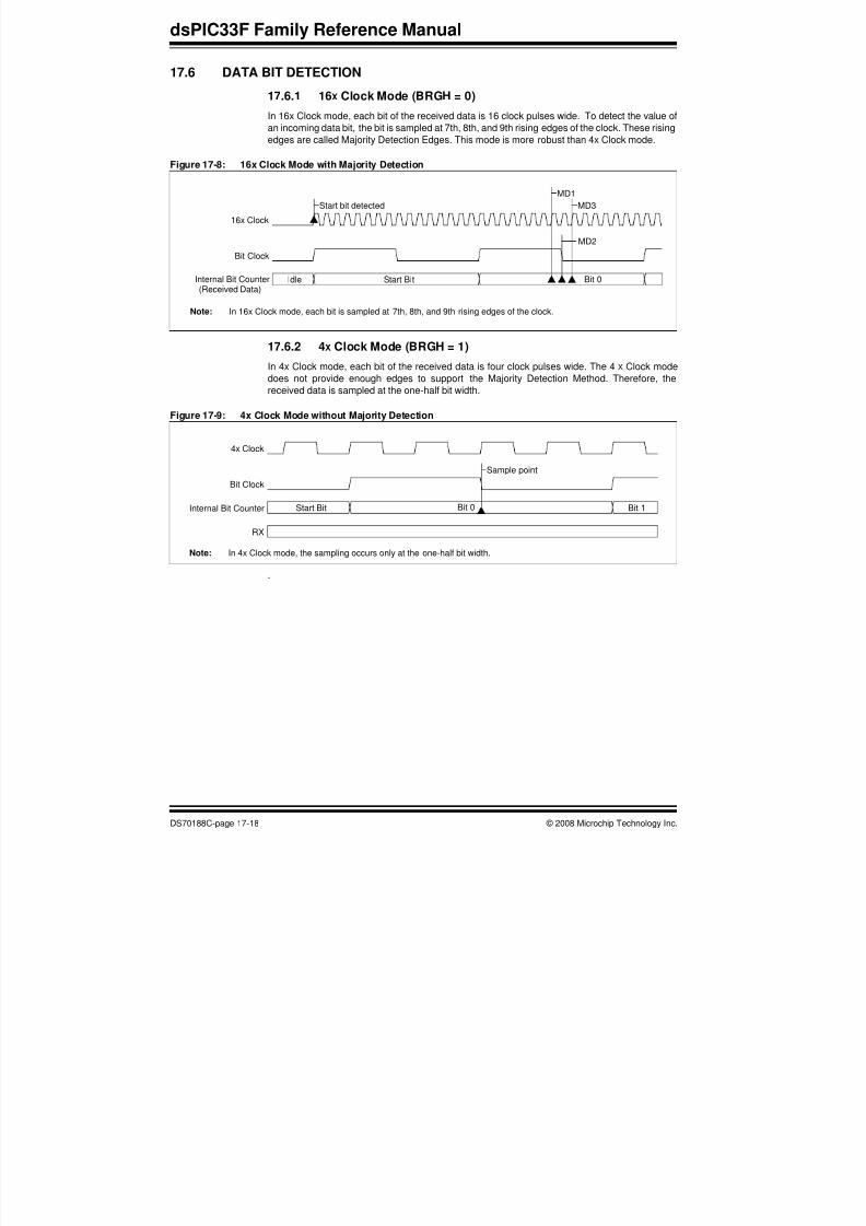
17.6.1 16X Clock Mode (BRGH = 0)
In 16x Clock mode, each bit of the received data is 16 clock pulses wide. To detect the value of
an incoming data bit, the bit is sampled at 7th, 8th, and 9th rising edges of the clock. These rising
edges are called Majority Detection Edges. This mode is more robust than 4x Clock mode.
Figure 17-8: 16x Clock Mode with Majority Detection
17.6.2 4X Clock Mode (BRGH = 1)
In 4x Clock mode, each bit of the received data is four clock pulses wide. The 4X Clock mode
does not provide enough edges to support the Majority Detection Method. Therefore, the
received data is sampled at the one-half bit width.
Figure 17-9: 4x Clock Mode without Majority Detection
.
Note: In 16x Clock mode, each bit is sampled at 7th, 8th, and 9th rising edges of the clock.
Idle Start Bit Bit 0
MD2
MD3
MD1
Start bit detected
16x Clock
Bit Clock
Internal Bit Counter(Received Data)
Start Bit Bit 0 Bit 1
Sample point
4x Clock
Bit Clock
Internal Bit Counter
RX
Note: In 4x Clock mode, the sampling occurs only at the one-half bit width.

8/2/2019 Family Reference Manual p17 - UART
http://slidepdf.com/reader/full/family-reference-manual-p17-uart 19/42
© 2008 Microchip Technology Inc. DS70188C-page 17-19
Section 17. UART
17.7 UART RECEIVER
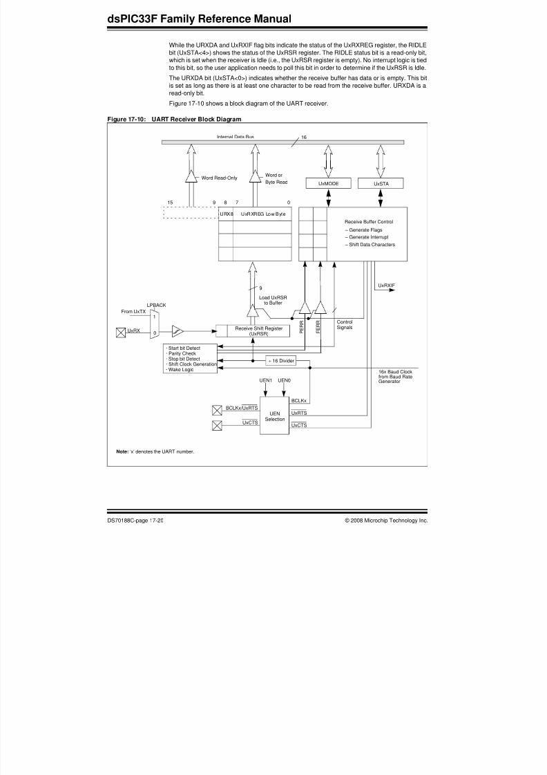
The block diagram of the receiver is shown in Figure 17-10. The heart of the receiver is the
Receive (Serial) Shift (UxRSR) register. The data is received on the UxRX pin and is sent to the
data recovery block. The data recovery block operates at 16 times the baud rate, whereas the
main receive serial shifter operates at the baud rate. After sampling the UxRX pin for the Stop
bit, the received data in UxRSR is transferred to the receive FIFO (if it is empty).
The data on the UxRX pin is sampled multiple times by a majority detect circuit to determine if a
high or a low level is present at the UxRX pin.
17.7.1 Receive Buffer (UxRXREG)
The UART receiver has a 4-deep, 9-bit wide FIFO receive data buffer. UxRXREG is a memory
mapped register that provides access to the output of the FIFO. It is possible for four words of
data to be received and transferred to the FIFO and a fifth word to begin shifting to the UxRSR
register before a buffer overrun occurs.
17.7.2 Receiver Error Handling
If the FIFO is full (four characters) and a fifth character is fully received into the UxRSR register,
the Overrun Error OERR (UxSTA<1>) bit will be set. The word in UxRSR will be kept, but furthertransfers to the receive FIFO are inhibited as long as the OERR bit is set. The user application
must clear the OERR bit in software to allow further data to be received.
If it is desired to keep the data received prior to the overrun, the user application should first read
all five characters, then clear the OERR bit. If the five characters can be discarded, the user
application can simply clear the OERR bit. This effectively resets the receive FIFO, and all prior
received data is lost.
The Framing Error bit, FERR (UxSTA<2>), is set if a Stop bit is detected at a logic low level.
The Parity Error bit, PERR (UxSTA<3>), is set if a parity error has been detected in the data word
at the top of the buffer (i.e., the current word). For example, a parity error would occur if the parity
is set to be Even, but the total number of ‘1’s in the data has been detected to be Odd. The PERRbit is irrelevant in the 9-bit mode. The FERR and PERR bits are buffered along with the
corresponding word and should be read before reading the data word.
An interrupt is generated if any of these (OERR, FERR and PERR) errors occur. The user
application needs to enable the corresponding Interrupt Enable Control bit (IEC4<UxERIE>) to
go to the corresponding interrupt vector location.
17.7.3 Receive Interrupt
The UART Receive Interrupt Flag (UxRXIF) is located in the corresponding Interrupt Flag Status
(IFS) register. The URXISEL<1:0> (UxSTA<7:6>) control bits determine when the UART receiver
generates an interrupt.
a) If URXISEL<1:0> = 00 or 01, an interrupt is generated each time a data word is transferred
from the Receive Shift (UxRSR) register to the receive buffer. There may be one or more
characters in the receive buffer.
b) If URXISEL<1:0> = 10, an interrupt is generated when a word is transferred from the UxRSR
register to the receive buffer, and as a result, the receive buffer contains 3 or 4 characters.
c) If URXISEL<1:0> = 11, an interrupt is generated when a word is transferred from the UxRSR
register to the receive buffer, and as a result, the receive buffer contains 4 characters (i.e.,
becomes full).
Switching between the three Interrupt modes during operation is possible.
Note: The UxRSR register is not mapped in data memory, so it is not available to the user
application.
Note: The data in the receive FIFO should be read prior to clearing the OERR bit. The
FIFO is reset when OERR is cleared, which causes all data in the buffer to be lost.
8/2/2019 Family Reference Manual p17 - UART
http://slidepdf.com/reader/full/family-reference-manual-p17-uart 20/42
dsPIC33F Family Reference Manual
DS70188C-page 17-20 © 2008 Microchip Technology Inc.
While the URXDA and UxRXIF flag bits indicate the status of the UxRXREG register, the RIDLE
bit (UxSTA<4>) shows the status of the UxRSR register. The RIDLE status bit is a read-only bit,
which is set when the receiver is Idle (i.e., the UxRSR register is empty). No interrupt logic is tied
to this bit, so the user application needs to poll this bit in order to determine if the UxRSR is Idle.
The URXDA bit (UxSTA<0>) indicates whether the receive buffer has data or is empty. This bit
is set as long as there is at least one character to be read from the receive buffer. URXDA is a
read-only bit.
Figure 17-10 shows a block diagram of the UART receiver.
Figure 17-10: UART Receiver Block Diagram
URX8 UxRXREG Low Byte
Load UxRSR
UxMODE
Receive Buffer Control
– Generate Flags
– Generate Interrupt
UxRXIF
UxRX
· Start bit Detect
Receive Shift Register
ControlSignals
16x Baud Clockfrom Baud RateGenerator
UxSTA
– Shift Data Characters
to Buffer
9
(UxRSR) P E R R
F E R R
· Parity Check· Stop bit Detect· Shift Clock Generation· Wake Logic
16Internal Data Bus
1
0
LPBACK
From UxTX
15 9 8 7 0
Word Read-OnlyWord or
Byte Read
BCLKx/UxRTS
UxCTS Selection
UEN
BCLKx
UEN1 UEN0
÷ 16 Divider
UxRTS
UxCTS
Note: ‘x’ denotes the UART number.
8/2/2019 Family Reference Manual p17 - UART
http://slidepdf.com/reader/full/family-reference-manual-p17-uart 21/42
© 2008 Microchip Technology Inc. DS70188C-page 17-21
Section 17. UART
17.7.4 Setup for UART Reception
Use the following steps when setting up a reception:
1. Initialize the UxBRG register for the appropriate baud rate (see 17.3 “UART Baud Rate
Generator”).
2. Set the number of data bits, number of Stop bits, and parity selection by writing to the
PDSEL<1:0> (UxMODE<2:1>) and STSEL (UxMODE<0>) bits.
3. If interrupts are desired, set the UxRXIE bit in the corresponding Interrupt Enable Control(IEC) register.
Specify the interrupt priority for the interrupt using the UxRXIP<2:0> control bits in the cor-
responding Interrupt Priority Control register (IPC). Also, select the Receive Interrupt
mode by writing to the URXISEL<1:0> (UxSTA<7:6>) bits.
4. Enable the UART module by setting the UARTEN (UxMODE<15>) bit.
5. Receive interrupts will depend on the URXISEL<1:0> control bit settings.
If receive interrupts are not enabled, the user application can poll the URXDA bit. The
UxRXIF bit should be cleared in the software routine that services the UART receive inter-
rupt.
6. Read data from the receive buffer.
If 9-bit transmission has been selected, read a word; otherwise, read a byte. The URXDA
status bit (UxSTA<0>) will be set whenever data is available in the buffer.Example 17-3 provides sample code that sets up the UART for reception.
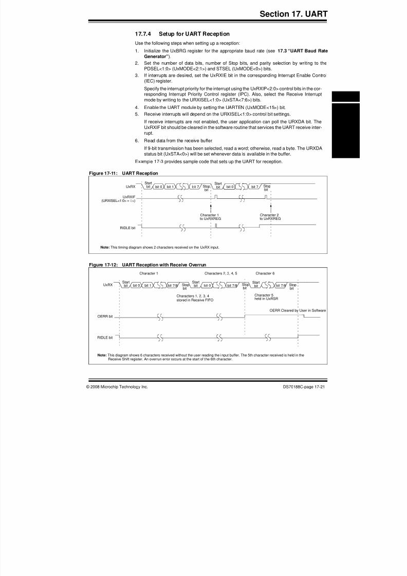
Figure 17-11: UART Reception
Figure 17-12: UART Reception with Receive Overrun
Startbit bit 1bit 0 bit 7 bit 0Stop
bit
Startbit bit 7 Stop
bitUxRX
RIDLE bit
Character 1to UxRXREG
Character 2to UxRXREG
Note: This timing diagram shows 2 characters received on the UxRX input.
UxRXIF(URXISEL<1:0> = 0x)
Startbit bit 7/8bit 1bit 0 bit 7/8 bit 0Stop
bit
Startbit
Startbitbit 7/8 Stop
bitUxRX
OERR bit
RIDLE bit
Characters 1, 2, 3, 4stored in Receive FIFO
Character 5held in UxRSR
Stopbit
Character 1 Characters 2, 3, 4, 5 Character 6
OERR Cleared by User in Software
Note: This diagram shows 6 characters received without the user reading the input buffer. The 5th character received is held in theReceive Shift register. An overrun error occurs at the start of the 6th character.

8/2/2019 Family Reference Manual p17 - UART
http://slidepdf.com/reader/full/family-reference-manual-p17-uart 22/42
dsPIC33F Family Reference Manual
DS70188C-page 17-22 © 2008 Microchip Technology Inc.
Example 17-3: UART Receiving with Polling (Interrupts Disabled)
#define FCY 40000000
#define BAUDRATE 9600
#define BRGVAL ((FCY/BAUDRATE)/16)-1
int main(void)
{
// Configure Oscillator to operate the device at 40Mhz
// Fosc= Fin*M/(N1*N2), Fcy=Fosc/2
// Fosc= 8M*40(2*2)=80Mhz for 8M input clock
PLLFBD=38; // M=40
CLKDIVbits.PLLPOST=0; // N1=2
CLKDIVbits.PLLPRE=0; // N2=2
OSCTUN=0; // Tune FRC oscillator, if FRC is used
RCONbits.SWDTEN=0; // Disable Watch Dog Timer
while(OSCCONbits.LOCK!=1) {}; // Wait for PLL to lock
U1MODEbits.STSEL = 0; // 1-stop bit
U1MODEbits.PDSEL = 0; // No Parity, 8-data bits
U1MODEbits.ABAUD = 0; // Auto-Baud Disabled
U1MODEbits.BRGH = 0; // Low Speed mode
U1BRG = BRGVAL; // BAUD Rate Setting for 9600
U1STAbits.URXISEL = 0; // Interrupt after one RX character is received;
U1MODEbits.UARTEN = 1; // Enable UART
while(1)
{
char ReceivedChar;
/* check for receive errors */
if(U1STAbits.FERR == 1)
{
continue;}
/* must clear the overrun error to keep uart receiving */
if(U1STAbits.OERR == 1)
{
U1STAbits.OERR = 0;
continue;
}
/* get the data */
if(U1STAbits.URXDA == 1)
{
ReceivedChar = U1RXREG;
}
}
8/2/2019 Family Reference Manual p17 - UART
http://slidepdf.com/reader/full/family-reference-manual-p17-uart 23/42
© 2008 Microchip Technology Inc. DS70188C-page 17-23
Section 17. UART
17.8 USING THE UART FOR 9-BIT COMMUNICATION
The UART receiver can be used in 9-bit Data mode for multiprocessor communication. With the
ADDEN bit set in 9-bit Data mode, the receiver can ignore the data when the 9th bit of the data
is ‘0’. This feature can be used in a multiprocessor environment.
17.8.1 Multiprocessor Communications
A typical multiprocessor communication protocol will differentiate between data bytes and
address/control bytes. A common scheme is to use a 9th data bit to identify whether a data byte
is address or data information. If the 9th bit is set, the data is processed as address or control
information. If the 9th bit is cleared, the received data word is processed as data associated with
the previous address/control byte.
The protocol operates as follows:
• The master device transmits a data word with the 9th bit set. The data word contains the
address of a slave device.
• All slave devices in the communication chain receive the address word and check the slave
address value.
• The slave device that was addressed will receive and process subsequent data bytes sent by
the master device. All other slave devices will discard subsequent data bytes until a new
address word (9th bit set) is received.
17.8.2 ADDEN Control Bit
The UART receiver has an Address Detect mode, which allows it to ignore data words with the
9th bit cleared. This reduces the interrupt overhead, since data words with the 9th bit cleared are
not buffered. This feature is enabled by setting the ADDEN bit (UxSTA<5>).
The UART must be configured for 9-bit Data mode to use the Address Detect mode. The ADDEN
bit has no effect when the receiver is configured in 8-bit Data mode.
17.8.3 Setup for 9-bit Transmit
The setup procedure for 9-bit transmission is identical to the procedure for 8-bit Transmit modes,
except that the PDSEL<1:0> bits (UxMODE<2:1) should be set to ‘11’ (see 17.5.3 “Setup for
UART Transmit”).
Word writes should be performed to the UxTXREG register (starts transmission).
8/2/2019 Family Reference Manual p17 - UART
http://slidepdf.com/reader/full/family-reference-manual-p17-uart 24/42
dsPIC33F Family Reference Manual
DS70188C-page 17-24 © 2008 Microchip Technology Inc.
17.8.4 Setup for 9-bit Reception Using Address Detect Mode
The setup procedure for 9-bit reception is similar to the procedure for 8-bit Receive modes,
except that the PDSEL<1:0> bits (UxMODE<2:1) should be set to ‘11’ (see 17.7.4 “Setup for
UART Reception”).
The Receive Interrupt mode should be configured by writing to the URXISEL<1:0> and
(UxSTA<7:6>) bits.
The procedure for using the Address Detect mode is as follows:
1. Set the ADDEN (UxSTA<5>) bit to enable address detect. Ensure that the URXISEL control
bits are configured to generate an interrupt after each received word.
2. Check each 8-bit address by reading the UxRXREG register to determine if the device is
being addressed.
3. If this device has not been addressed, discard the received word.
4. If this device has been addressed, clear the ADDEN bit to allow subsequent data bytes to
be read into the receive buffer and interrupt the CPU.
If a long data packet is expected, the Receive Interrupt mode could be changed to buffermore than one data byte between interrupts.
5. When the last data byte has been received, set the ADDEN bit so that only address bytes
will be received.
Also, ensure that the URXISEL control bits are configured to generate an interrupt after
each received word.
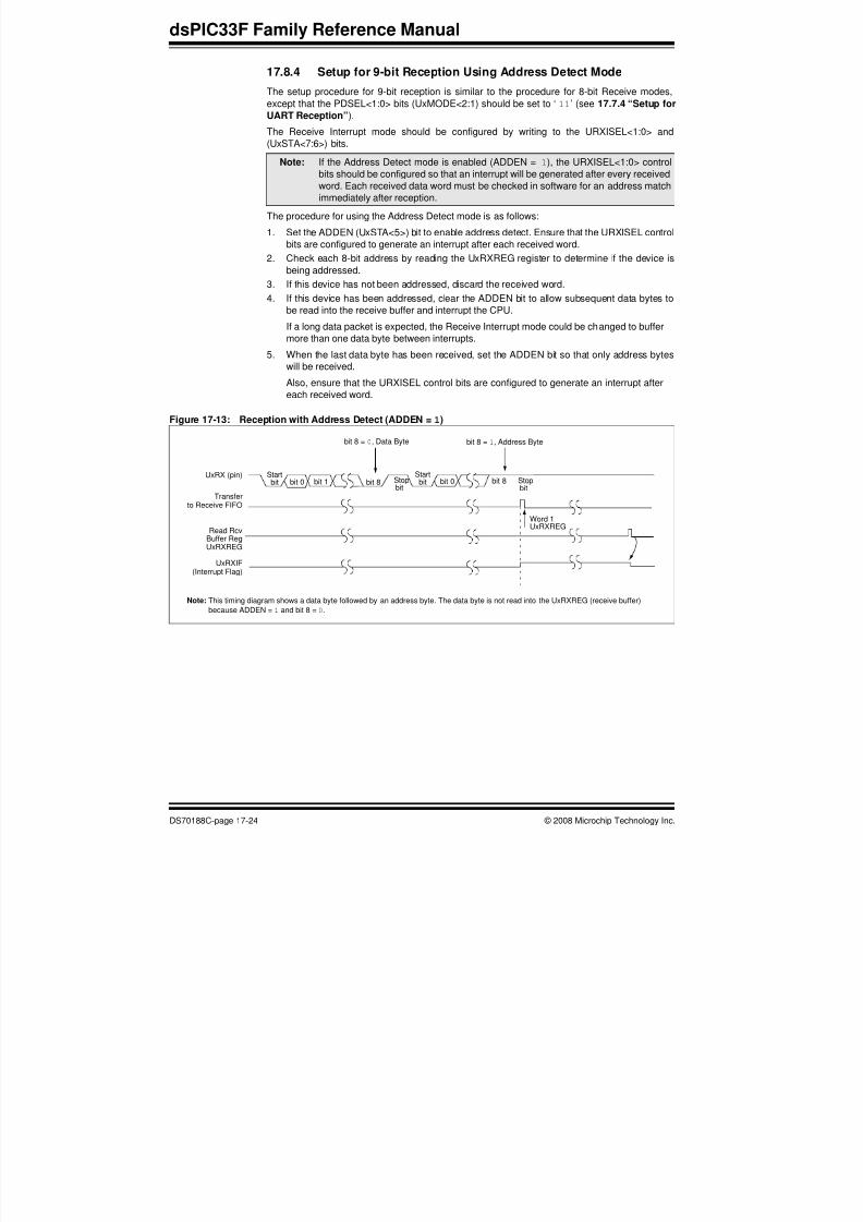
Figure 17-13: Reception with Address Detect (ADDEN = 1)
Note: If the Address Detect mode is enabled (ADDEN = 1), the URXISEL<1:0> controlbits should be configured so that an interrupt will be generated after every received
word. Each received data word must be checked in software for an address match
immediately after reception.
Startbit bit 1bit 0 bit 8 bit 0Stop
bit
Startbit bit 8 Stop
bit
UxRX (pin)
Read RcvBuffer RegUxRXREG
UxRXIF(Interrupt Flag)
Word 1UxRXREG
bit 8 = 0, Data Byte bit 8 = 1, Address Byte
Transferto Receive FIFO
Note: This timing diagram shows a data byte followed by an address byte. The data byte is not read into the UxRXREG (receive buffer)
because ADDEN = 1 and bit 8 = 0.
8/2/2019 Family Reference Manual p17 - UART
http://slidepdf.com/reader/full/family-reference-manual-p17-uart 25/42
© 2008 Microchip Technology Inc. DS70188C-page 17-25
Section 17. UART
17.9 OTHER FEATURES OF THE UART
17.9.1 UART in Loopback Mode
Setting the LPBACK bit enables the Loopback mode, in which the UxTX output is internally
connected to the UxRX input. When configured for the Loopback mode, the UxRX pin is
disconnected from the internal UART receive logic. However, the UxTX pin still functions
normally.
To select this mode, do the following:
1. Configure UART for the desired mode of operation.
2. Enable transmission as defined in 17.5 “UART Transmitter”.
3. Set LPBACK = 1 (UxMODE<6>) to enable Loopback mode.
The Loopback mode is dependent on the UEN<1:0> bits, as shown in Table 17-1.
Table 17-1: Loopback Mode Pin Function
17.9.2 Auto-Baud Support
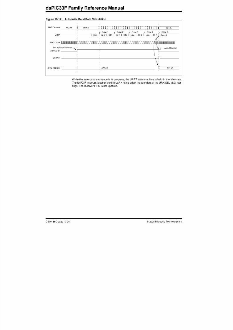
To allow the system to determine baud rates of the received characters, the ABAUD bit is
enabled. The UART will begin an automatic baud rate measurement sequence whenever a Start
bit is received while the Auto-Baud Rate Detect is enabled (ABAUD = 1). The calculation is
self-averaging. Once the ABAUD bit is set, the BRG counter value will be cleared and will lookfor a Start bit, which in this case, is defined as a high-to-low transition followed by a low-to-high
transition.
Following the Start bit, the auto-baud expects to receive an ASCII “U” (“55h”) in order to
calculate the proper bit rate. The measurement is taken over both the low and the high bit time
in order to minimize any effects caused by asymmetry of the incoming signal. On the 5th UxRX
pin rising edge, an accumulated BRG counter value totalling the proper BRG period is
transferred to the UxBRG register. The ABAUD bit is automatically cleared. If the user
application clears the ABAUD bit prior to sequence completion, unexpected module behavior
can result. Refer to Figure 17-14 for the Auto-Baud Rate Detection sequence.
UEN<1:0> Pin Function, LPBACK = 1(1)
00 UxRX input connected to UxTX; UxTX pin functions; UxRX pin ignored;
UxCTS/UxRTS unused
01 UxRX input connected to UxTX; UxTX pin functions; UxRX pin ignored;
UxRTS pin functions; UxCTS unused10 UxRX input connected to UxTX; UxTX pin functions; UxRX pin ignored;
UxRTS pin functions; UxCTS input connected to UxRTS; UxCTS pin ignored
11 UxRX input connected to UxTX; UxTX pin functions; UxRX pin ignored;
BCLKx pin functions; UxCTS/UxRTS unused
Note 1: The LPBACK bit should be set to ‘1’ only after enabling the other bits associated
with the UART module.
8/2/2019 Family Reference Manual p17 - UART
http://slidepdf.com/reader/full/family-reference-manual-p17-uart 26/42
dsPIC33F Family Reference Manual
DS70188C-page 17-26 © 2008 Microchip Technology Inc.
Figure 17-14: Automatic Baud Rate Calculation
While the auto-baud sequence is in progress, the UART state machine is held in the Idle state.
The UxRXIF interrupt is set on the 5th UxRX rising edge, independent of the URXISEL<1:0> set-
tings. The receiver FIFO is not updated.
BRG Counter
UxRX
ABAUD bit
bit 0 bit 1
BRG Clock
Start
Auto-ClearedSet by User Software
XXXXh 0000h
Edge 1
bit 2 bit 3
Edge 2
bit 4 bit 5
Edge 3
bit 6 bit 7
Edge 4
Stop bit
Edge 5
001Ch
BRG Register XXXXh 001Ch
UxRXIF

8/2/2019 Family Reference Manual p17 - UART
http://slidepdf.com/reader/full/family-reference-manual-p17-uart 27/42
© 2008 Microchip Technology Inc. DS70188C-page 17-27
Section 17. UART
17.10 UART OPERATION WITH DMA
On some dsPIC33F devices, the Direct Memory Access (DMA) module can be used to transfer
data between the CPU and UART without CPU assistance. Consult the dsPIC33F device data
sheet to see if DMA is present on your particular device. For more information on the DMA
module, see Section 22. “Direct Memory Access (DMA)” (DS701832) in the dsPIC33F Family
Reference Manual .
If the DMA channel is associated with the UART receiver, the UART will issue a DMA request
every time there is a character ready to be moved from UART to RAM. DMA will transfer datafrom the UxRXREG register into RAM and issue a CPU interrupt after a predefined number of
transfers. Similarly, if the DMA channel is associated with the UART transmitter, the UART will
issue a DMA request after each successful transmission. After each DMA request, the DMA
transfers new data into the UxTXREG register and issues a CPU interrupt after a predefined
number of transfers. Since DMA channels are unidirectional, two DMA channels are required if
the UART module is used for both receive and transmit. Each DMA channel must be initialized
as shown in Table 17-2:
Table 17-2: DMA Channel Register Initialization for UART to DMA Association
In addition, the UART must be configured to generate interrupts for every character received or
transmitted. For the UART receiver to generate an Rx interrupt for each character received, the
Receive Interrupt Mode Selection bits (URXISEL<1:0>) must be set to ‘00’ or ‘01’ in the Status
and Control (UxSTA) register. For the UART transmitter to generate a Tx interrupt for each
character transmitted, the Transmission Interrupt Mode Selection bits (UTXISEL0 and
UTXISEL1) must be set to ‘0’ in the UxSTA register.
When the UART and DMA channel are properly configured, the UART receiver issues a DMA
request as soon as data is received. No special steps need to be taken by the user applicationto initiate a DMA transfer. However, the UART transmitter issues a DMA request as soon as the
UART and transmitter are enabled. This means that the DMA channel and buffers must be
initialized and enabled before the UART and transmitter. Alternatively, the UART and UART
transmitter can be enabled before the DMA channel is enabled. In this case, the UART
transmitter DMA request will be lost, and the user application must issue a DMA request to start
DMA transfers by setting the FORCE bit in the DMAxREQ register.
Example 17-4 provides sample code for UART reception and transmission with the help of two
DMA channels. The UART receives and buffers characters from the hyperterminal at 9600 bps.
After 8 characters are received, the UART transmits (echoes) them back to the hyperterminal.
DMA Channel 0 is configured for UART transmission with the following configuration:
• Transfer data from RAM to UART
• One-Shot mode
• Register Indirect with Post-Increment• Using single buffer
• Eight transfers per buffer
• Transfer words
DMA Channel 1 is configured for UART reception with the following configuration:
• Transfer data from UART to RAM Continuously
• Register Indirect with Post-Increment
• Using two “ping-pong” buffers
• Eight transfers per buffer
• Transfer words
Peripheral to DMA
Association
DMAxREQ
Register
IRQSEL<6:0>
Bits
DMAxPAD Register
Values to Read
From Peripheral
DMAxPAD Register
Values to Write to
Peripheral
UART1RX–UART1 Receiver 0001011 0x0226 (U1RXREG) —
UART1TX–UART1 Transmitter 0001100 — 0x0224 (U1TXREG)
UART2RX–UART2 Receiver 0011110 0x0236 (U2RXREG) —
UART2TX–UART2 Transmitter 0011111 — 0x0234 (U2TXREG)

8/2/2019 Family Reference Manual p17 - UART
http://slidepdf.com/reader/full/family-reference-manual-p17-uart 28/42
dsPIC33F Family Reference Manual
DS70188C-page 17-28 © 2008 Microchip Technology Inc.
Example 17-4: UART Reception and Transmission with DMA
Set Up UART for Rx and Tx:
#define FCY 40000000
#define BAUDRATE 9600
#define BRGVAL ((FCY/BAUDRATE)/16)-1
U2MODEbits.STSEL = 0; // 1-stop bit
U2MODEbits.PDSEL = 0; // No Parity, 8-data bits
U2MODEbits.ABAUD = 0; // Auto-Baud Disabled
U2BRG = BRGVAL;// BAUD Rate Setting for 9600
U2STAbits.UTXISEL0 = 0; // Interrupt after one Tx character is transmitted
U2STAbits.UTXISEL1 = 0;
U2STAbits.URXISEL = 0; // Interrupt after one RX character is received
U2MODEbits.UARTEN = 1; // Enable UART
U2STAbits.UTXEN = 1; // Enable UART Tx
Set Up DMA Channel 0 to Transmit in One-Shot, Single-Buffer Mode:
unsigned int BufferA[8] __attribute__((space(dma)));
unsigned int BufferB[8] __attribute__((space(dma)));
DMA0CON = 0x2001; // One-Shot, Post-Increment, RAM-to-Peripheral
DMA0CNT = 7; // 8 DMA requests
DMA0REQ = 0x001F; // Select UART2 Transmitter
DMA0PAD = (volatile unsigned int) &U2TXREG;
DMA0STA = __builtin_dmaoffset(BufferA);
IFS0bits.DMA0IF = 0; // Clear DMA Interrupt Flag
IEC0bits.DMA0IE = 1; // Enable DMA interrupt
Set Up DMA Channel 1 to Receive in Continuous Ping-Pong Mode:
DMA1CON = 0x0002; // Continuous, Ping-Pong, Post-Inc., Periph-RAM
DMA1CNT = 7; // 8 DMA requests
DMA1REQ = 0x001E; // Select UART2 Receiver
DMA1PAD = (volatile unsigned int) &U2RXREG;
DMA1STA = __builtin_dmaoffset(BufferA);
DMA1STB = __builtin_dmaoffset(BufferB);
IFS0bits.DMA1IF = 0; // Clear DMA interrupt
IEC0bits.DMA1IE = 1; // Enable DMA interrupt
DMA1CONbits.CHEN = 1; // Enable DMA Channel
8/2/2019 Family Reference Manual p17 - UART
http://slidepdf.com/reader/full/family-reference-manual-p17-uart 29/42
© 2008 Microchip Technology Inc. DS70188C-page 17-29
Section 17. UART
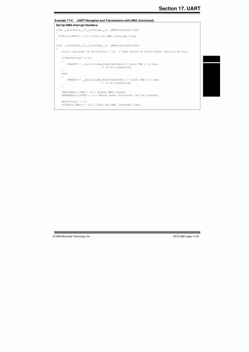
Example 17-4: UART Reception and Transmission with DMA (Continued)
Set Up DMA Interrupt Handlers:
void __attribute__((__interrupt__)) _DMA0Interrupt(void)
{
IFS0bits.DMA0IF = 0;// Clear the DMA0 Interrupt Flag;
}
void __attribute__((__interrupt__)) _DMA1Interrupt(void)
{
static unsigned int BufferCount = 0; // Keep record of which buffer contains Rx Data
if(BufferCount == 0)
{
DMA0STA = __builtin_dmaoffset(BufferA);// Point DMA 0 to data
// to be transmitted
}
else
{
DMA0STA = __builtin_dmaoffset(BufferB); // Point DMA 0 to data
// to be transmitted
}
DMA0CONbits.CHEN = 1;// Enable DMA0 Channel
DMA0REQbits.FORCE = 1;// Manual mode: Kick-start the 1st transfer
BufferCount ^= 1;
IFS0bits.DMA1IF = 0;// Clear the DMA1 Interrupt Flag}
8/2/2019 Family Reference Manual p17 - UART
http://slidepdf.com/reader/full/family-reference-manual-p17-uart 30/42
dsPIC33F Family Reference Manual
DS70188C-page 17-30 © 2008 Microchip Technology Inc.
17.11 UART OPERATION DURING CPU SLEEP AND IDLE MODES
17.11.1 UART Operation in Sleep Mode
When the device enters Sleep mode, all clock sources supplied to the UART module are shut
down and stay at logic ‘0’. If the device enters Sleep mode in the middle of a UART transmission
or reception operation, the operation is aborted and the UART pins (BCLKx, UxRTS, and UxTX)
are driven to the default state.
A Start bit, when detected on the UART Receive (UxRX) pin, can wake up the device from Sleepmode if the WAKE bit (UxMODE<7>) is set just before the device enters Sleep mode. In this
mode, if the UART receive interrupt (UxRXIE) is enabled, a falling edge on the UART Receive
pin generates a UART receive interrupt (UxRXIF).
The receive interrupt wakes up the device from Sleep, and the following occurs:
• If the assigned priority for the interrupt is less than, or equal, to the current CPU priority, the
device wakes up and continues code execution from the instruction following the PWRSAV
instruction that initiated Sleep mode.
• If the assigned priority level for the interrupt source is greater than the current CPU priority,
the device wakes up and the CPU exception process begins. Code execution continues
from the first instruction of the capture ISR.
The WAKE bit is automatically cleared when a low-to-high transition is observed on the UxRX
line following the wake-up event.
17.11.2 UART Operation in Idle Mode
When the device enters Idle mode, the system clock sources remain functional and the CPU
stops code execution. The UART Stop-in Idle (USIDL) bit in the UART Mode (UxMODE<13>)
register determines whether the module stops in Idle mode or continues to operate in Idle mode.
• If USIDL = 0 (UxMODE<13>), the module continues to operate in Idle mode and provides
full functionality.
• If USIDL = 1 (UxMODE<13>), the module stops in Idle mode. The module performs the
same functions when stopped in Idle mode as in Sleep mode (refer to 17.11.1 “UART
Operation in Sleep Mode”).
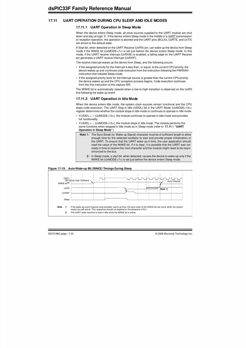
Figure 17-15: Auto-Wake-up Bit (WAKE) Timings During Sleep
Note 1: The Sync Break (or Wake-up Signal) character must be of sufficient length to allow
enough time for the selected oscillator to start and provide proper initialization of
the UART. To ensure that the UART woke up in time, the user application shouldread the value of the WAKE bit. If it is clear, it is possible that the UART was not
ready in time to receive the next character and the module might need to be resyn-
chronized to the bus.
2: In Sleep mode, a start bit, when detected, causes the device to wake-up only if the
WAKE bit (UxMODE<7>) is set just before the device enters Sleep mode.
OSC1
WAKE bit(2)
UxRX
UxRXIF
Sleep
Note 1: If the wake-up event requires long oscillator warm-up time, the auto-clear of the WAKE bit can occur while the systemclocks are still active. This sequence should not depend on the presence of FCY.
2: The UART state machine is held in Idle while the WAKE bit is active.
(Note 1)
Bit Set by User Software Auto-Cleared
8/2/2019 Family Reference Manual p17 - UART
http://slidepdf.com/reader/full/family-reference-manual-p17-uart 31/42
© 2008 Microchip Technology Inc. DS70188C-page 17-31
Section 17. UART
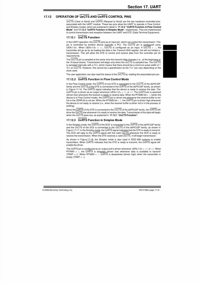
17.12 OPERATION OF UxCTS AND UxRTS CONTROL PINS
UxCTS (Clear to Send) and UxRTS (Request to Send) are the two hardware controlled pins
associated with the UART module. These two pins allow the UART to operate in Flow Control
and Simplex modes, which are explained in detail in 17.12.2 “UxRTS Function in Flow Control
Mode” and 17.12.3 “UxRTS Function in Simplex Mode”, respectively. They are implemented
to control transmission and reception between the UART and DTE (Data Terminal Equipment).
17.12.1 UxCTS FunctionIn the UART operation, the UxCTS acts as an input pin, which can control the transmission. This
pin is controlled by another device (typically a PC). The UxCTS pin is configured using
UEN<1:0>. When UEN<1:0> = 10, UxCTS is configured as an input. If UxCTS = 1, the
transmitter will go as far as loading the data in the Transmit Shift register, but will not initiate a
transmission. This will allow the DTE to control and receive data from the controller per its
requirements.
The UxCTS pin is sampled at the same time the transmit data changes (i.e., at the beginning of
the 16 baud clocks). Transmission will begin only when the UxCTS is sampled low. The UxCTS
is sampled internally with a TCY, which means that there should be a minimum pulse width of 1
TCY on UxCTS. However, this cannot be a specification as the TCY can vary depending on the
clock used.
The user application can also read the status of the UxCTS by reading the associated port pin.
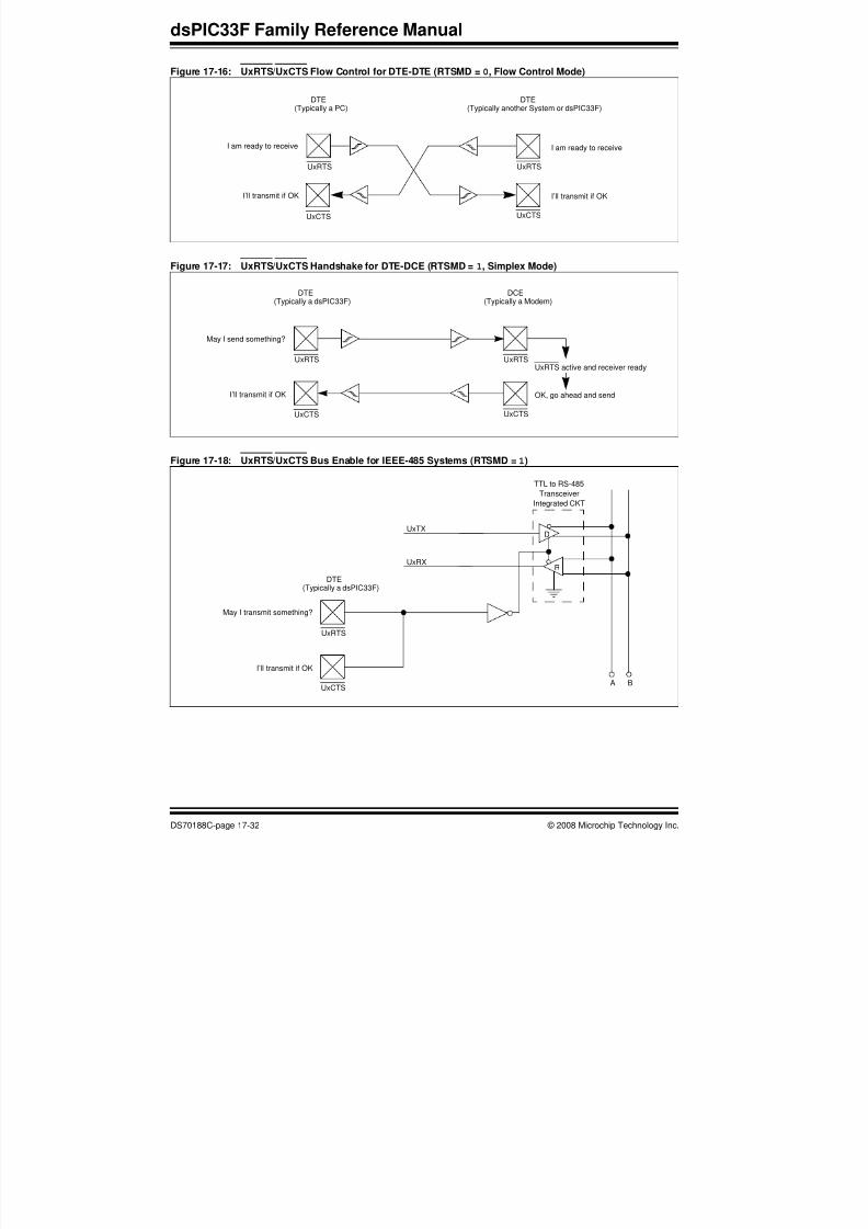
17.12.2 UxRTS Function in Flow Control Mode
In the Flow Control mode, the UxRTS of one DTE is connected to the UxCTS of the dsPIC33F
family and the UxCTS of the DTE is connected to the UxRTS of the dsPIC33F family, as shown
in Figure 17-16. The UxRTS signal indicates that the device is ready to receive the data. The
UxRTS pin is driven as an output whenever UEN<1:0> = 01 or 10. The UxRTS pin is asserted
(driven low) whenever the receiver is ready to receive data. When the RTSMD bit = 0 (when the
device is in Flow Control mode), the UxRTS pin is driven low whenever the receive buffer is not
full or the OERR bit is not set. When the RTSMD bit = 0, the UxRTS pin is driven high whenever
the device is not ready to receive (i.e., when the receiver buffer is either full or in the process of
shifting).
Since the UxRTS of the DTE is connected to the UxCTS of the dsPIC33F family, the UxRTS will
drive the UxCTS low whenever it is ready to receive the data. Transmission of the data will begin
when the UxCTS goes low, as explained in 17.12.1 “UxCTS Function”.
17.12.3 UxRTS Function in Simplex Mode
In the Simplex mode, the UxRTS of the DCE is connected to the UxRTS of the dsPIC33F family
and the UxCTS of the DCE is connected to the UxCTS of the dsPIC33F family, as shown in
Figure 17-17. In the Simplex mode, the UxRTS signal indicates that the DTE is ready to transmit.
The DCE will reply to the UxRTS signal with the valid UxCTS whenever the DCE is ready to
receive the transmission. When the DTE receives a valid UxCTS, it will begin transmission.
As shown in Figure 17-18, the Simplex mode is also used in IEEE-485 systems to enable
transmitters. When UxRTS indicates that the DTE is ready to transmit, the UxRTS signal will
enable the driver.
The UxRTS pin is configured as an output and is driven whenever UEN<1:0> = 01 or 10. When
RTSMD = 1, the UxRTS is asserted (driven low) whenever data is available to transmit
(TRMT = 0). When RTSMD = 1, UxRTS is deasserted (driven high) when the transmitter is
empty (TRMT = 1).
8/2/2019 Family Reference Manual p17 - UART
http://slidepdf.com/reader/full/family-reference-manual-p17-uart 32/42
dsPIC33F Family Reference Manual
DS70188C-page 17-32 © 2008 Microchip Technology Inc.
Figure 17-16: UxRTS/UxCTS Flow Control for DTE-DTE (RTSMD = 0, Flow Control Mode)
Figure 17-17: UxRTS/UxCTS Handshake for DTE-DCE (RTSMD = 1, Simplex Mode)
Figure 17-18: UxRTS/UxCTS Bus Enable for IEEE-485 Systems (RTSMD = 1)
UxRTS UxRTS
UxCTS UxCTS
DTE(Typically a PC)
DTE(Typically another System or dsPIC33F)
I am ready to receive
I’ll transmit if OK
I am ready to receive
I’ll transmit if OK
UxRTS UxRTS
UxCTS UxCTS
DTE(Typically a dsPIC33F)
DCE(Typically a Modem)
May I send something?
UxRTS active and receiver ready
I’ll transmit if OK OK, go ahead and send
UxRTS
UxCTS
DTE(Typically a dsPIC33F)
May I transmit something?
I’ll transmit if OK
UxTX
UxRX
D
R
BA
TTL to RS-485
Transceiver
Integrated CKT
8/2/2019 Family Reference Manual p17 - UART
http://slidepdf.com/reader/full/family-reference-manual-p17-uart 33/42
© 2008 Microchip Technology Inc. DS70188C-page 17-33
Section 17. UART
17.13 INFRARED SUPPORT
The UART module provides two types of infrared UART support: one is the IrDA clock output to
support the external IrDA encoder and decoder devices (legacy module support), and the other
is the full implementation of the IrDA encoder and decoder.
17.13.1 External IrDA Support – IrDA Clock Output
To support external IrDA encoder and decoder devices, the BCLKx pin can be configured to
generate the 16x baud clock. When UEN<1:0> = 11, the BCLKx pin will output the 16x baud
clock if the UART module is enabled; it can be used to support the IrDA codec chip.
17.13.2 Built-In IrDA Encoder and Decoder
The UART has full implementation of the IrDA encoder and decoder as part of the UART module.
The built-in IrDA encoder and decoder functionality is enabled using the IREN bit
(UxMODE<12>). When enabled (IREN = 1), the receive pin (UxRX) acts as the input from the
infrared receiver. The transmit pin (UxTX) acts as the output to the infrared transmitter.
17.13.2.1 IrDA ENCODER FUNCTION
The encoder works by taking the serial data from the UART and replacing it as explained below.
Transmit bit data of ‘1’ gets encoded as ‘0’ for the entire 16 periods of the 16x baud clock.
Transmit bit data of ‘0’ gets encoded as ‘0’ for the first 7 periods of the 16x baud clock, as ‘1’ for
the next 3 periods and as ‘0’ for the remaining 6 periods. See Figure 17-19 and Figure 17-21 for
details.
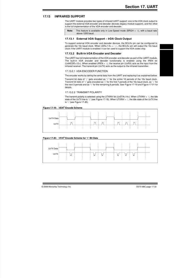
17.13.2.2 TRANSMIT POLARITY
The transmit polarity is selected using the UTXINV bit (UxSTA<14>). When UTXINV = 0, the Idle
state of the UxTX line is ‘0’ (see Figure 17-19). When UTXINV = 1, the Idle state of the UxTX line
is ‘1’ (see Figure 17-20).
Figure 17-19: IrDA ® Encode Scheme
Figure 17-20: IrDA ® Encode Scheme for ‘0’ Bit Data
Note: This feature is available only in Low-Speed mode (BRGH = 0), with a baud rate
above 1200 baud.
UxTX Data
UxTX
UxTX Data
UxTX

8/2/2019 Family Reference Manual p17 - UART
http://slidepdf.com/reader/full/family-reference-manual-p17-uart 34/42
dsPIC33F Family Reference Manual
DS70188C-page 17-34 © 2008 Microchip Technology Inc.
Figure 17-21: IrDA ® Encode Scheme for ‘0’ Bit Data with Respect to 16x Baud Clock
17.13.2.3 IrDA DECODER FUNCTION
The decoder works by taking the serial data from the UxRX pin and replacing it with the
decoded data stream. The stream is decoded based on falling edge detection of the UxRX
input.
Each falling edge of UxRX causes the decoded data to be driven low for 16 periods of the
16x baud clock. If, by the time the 16 periods expire, another falling edge has been detected,
the decoded data remains low for another 16 periods. If no falling edge was detected, the
decoded data is driven high.
Note that the data stream into the device is shifted anywhere from 7 to 8 periods of the
16x baud clock from the actual message source. The one clock uncertainty is due to the clock
edge resolution (see Figure 17-22 for details).
Figure 17-22: IrDA ® Decoding Scheme
Start ofStart of
‘0’ Transmit bit
16x Baud Clock
UxTX Data
UxTX
8th Period 11th Period
16 Periods 16 Periods 16 Periods 16 Periods 16 Periods
Start BRG TIRDEL
Before IrDA ® Encoder
UxRX
Decoded Data
(Transmitting Device)

8/2/2019 Family Reference Manual p17 - UART
http://slidepdf.com/reader/full/family-reference-manual-p17-uart 35/42
© 2008 Microchip Technology Inc. DS70188C-page 17-35
Section 17. UART
17.13.2.4 IrDA RECEIVE POLARITY
The input of the IrDA signal can have an inverted polarity. The same logic is able to decode the
signal train, but in this case, the decoded data stream is shifted from 10 to 11 periods of the
16x baud clock from the original message source. Again, the one clock uncertainty is due to the
clock edge resolution (see Figure 17-23 for details).
Figure 17-23: Inverted Polarity Decoding Results
17.13.2.5 CLOCK JITTER
Due to jitter, or slight frequency differences between devices, it is possible for the next falling bitedge to be missed for one of the 16x periods. In that case, a one clock wide pulse appears on
the decoded data stream. Since the UART performs a majority detect around the bit center, this
does not cause erroneous data (see Figure 17-24 for details).
Figure 17-24: Clock Jitter Causing a Pulse Between Consecutive Zeros
16 Periods 16 Periods 16 Periods 16 Periods 16 Periods
Start BRG TIRDELI
Before IrDA ® Encoder
UxRX
Decoded Data
(Transmitting Device)
16 Periods 16 Periods
Extra Pulse will be Ignored
UxRX (rx_in)
Decoded Data

8/2/2019 Family Reference Manual p17 - UART
http://slidepdf.com/reader/full/family-reference-manual-p17-uart 36/42
dsPIC33F Family Reference Manual
DS70188C-page 17-36 © 2008 Microchip Technology Inc.
17.14 LIN SUPPORT
17.14.1 Introduction
The LIN protocol transmits data in the form of small blocks, known as frames. Each frame
consists of a Break character with a delimiter, a Synch byte, a protected identifier, and the data
to be transmitted (see Figure 17-25).
• Break Sequence: The break sequence indicates the beginning of a new frame. A break
sequence generated by the master node consists of a Start bit followed by twelve bits of ‘0’and a break delimiter.
• Synch Byte: The Synch is a byte field loaded with the data value of 0x55. When the
Auto-Baud feature is enabled, the UART module uses the Synch byte to compute the baud
rate of the incoming data.
• Protected Identifier: The Protected Identifier contains the identifier and the identifier parity.
Figure 17-25: Frame Structure
17.14.2 Data Reception Using LIN Protocol
When the LIN protocol is used, the UART module receives data in the form of frames and the
incoming data is loaded into the receive buffer. For effective data reception, the BRG counter
should be loaded with the baud rate of incoming data.
The bit rate of the incoming data can be detected, if the following occurs:
• The Auto-Baud feature is enabled
• The WAKE bit is set before setting the ABAUD bit
The UART module uses the Synch byte to compute the baud rate of the incoming data. If the
WAKE bit is set before setting the ABAUD bit, the Auto-Baud Rate Detection occurs on the byte
following the Break Character. The module receives the Start bit of the Break Character, the data
and the invalid Stop bit (which sets FERR), but the receiver waits for a valid Stop bit before receiv-
ing the next Start bit. No further reception can occur until a Stop bit is received.The WAKE bit isautomatically cleared once the Stop bit is received. After the fifth rising edge of the Synch
character is detected, the baud rate of the incoming data is loaded into the BRG counter and the
ABAUD bit is automatically cleared.
If the Auto-Baud feature is enabled without setting the WAKE bit, the delimiter is assumed to be
the first bit of the Synch byte instead of the Start bit. This results in erroneous baud rate
calculation. This happens because the receiver expects a Synch byte at the start of the reception.
The LIN protocol, however, initiates the transmission with the Break character and the Synch
byte follows. Thus, the delimiter, which can range from one to four bits, is assumed to be the first
low-to-high transition on the Rx line. Therefore, the delimiter acts as a first bit of the Synch byte
instead of the Start bit (see Figure 17-26).
UxRX bit 0 bit 1Start bit 2 bit 3 bit 4 bit 5 bit 6 bit 7 Stop bitDelimiter
Break Character Synch Byte
Identifier, Dataand Checksum
Note: Before data reception, the user application should load the BRG counter of the
UART module with a value approximate to the bit rate of the incoming data.

8/2/2019 Family Reference Manual p17 - UART
http://slidepdf.com/reader/full/family-reference-manual-p17-uart 37/42
© 2008 Microchip Technology Inc. DS70188C-page 17-37
Section 17. UART
Figure 17-26: Data Reception Using the LIN Protocol
Break Character
BRG Counter
UxRX bit 0 bit 1Start
XXXXh 0000h
Edge 1
bit 2 bit 3Edge 2
bit 4 bit 5Edge 3
bit 6 bit 7Edge 4
Stop bit
Edge 5
001Ch
Identifier, Dataand Checksum
Delimiter
Synch Byte
1 6
1. The user application first sets the WAKE bit and then the ABAUD bit.
2. An Rx interrupt is generated because device wakes up on the reception of the Break character.
3. The FERR bit is set.
4. The WAKE bit is cleared.
5. The Auto-Baud feature detects the first rising edge of the Synch byte.
6. The fifth rising edge of the Synch byte is detected. The ABAUD bit is cleared and the BRG counter is loaded with the
baud rate of the received data.
Auto-ClearedWAKE bit
ABAUD bit
UxRXIF
52 3 4
Auto-Cleared

8/2/2019 Family Reference Manual p17 - UART
http://slidepdf.com/reader/full/family-reference-manual-p17-uart 38/42
D S 7 0 1 8 8 C - p a g e1 7 - 3 8
©
2 0 0 8 Mi c r
o c h i pT e c h n ol o g y I n c .
17.15 REGISTERS MAP
A summary of the registers associated with the dsPIC33F family UARTx is provided in Table 17-3
Table 17-3: Registers Associated with UARTx
SFR Name Bit 15 Bit 14 Bit 13 Bit 12 Bit 11 Bit 10 Bit 9 Bit 8 Bit 7 Bit 6 Bit 5 Bit 4 Bit
UxMODE UARTEN — USIDL IREN RTSMD — UEN<1:0> WAKE LPBACK ABAUD URXINV BRG
UxSTA UTXISEL1 UTXINV UTXISEL0 — UTXBRK UTXEN UTXBF TRMT URXISEL<1:0> ADDEN RIDLE PER
UxTXREG — — — — — — — UTX8 Transmit Register
UxRXREG — — — — — — — URX8 Receive Register
UxBRG Baud Rate Generator Prescaler
IFS0 — — — U1TXIF U1RXIF — — — — — — — —
IFS1 U2TXIF U2RXIF — — — — — — — — — — —
IFS4 — — — — — — — — — — — — —
IEC0 — — — U1TXIE U1RXIE — — — — — — — —
IEC1 U2TXIE U2RXIE — — — — — — — — — — —
IEC4 — — — — — — — — — — — — —
IPC2 — U1RXIP<2:0> — — — — — — — — —
IPC3 — — — — — — — — — — — — —
IPC7 — U2TXIP<2:0> — U2RXIP<2:0> — — — — —
IPC16 — — — — — U2EIP<2:0> — U1EIP<2:0> —
Note: The registers associated with UARTx are shown for reference. See the device data sheet for the registers associated with other UART modules.

8/2/2019 Family Reference Manual p17 - UART
http://slidepdf.com/reader/full/family-reference-manual-p17-uart 39/42
© 2008 Microchip Technology Inc. DS70188C-page 17-39
Section 17. UART
17.16 DESIGN TIPS
Question 1: The data I transmit with the UART does not get received correctly. What
could cause this?
Answer: The most common reason for reception errors is that an incorrect value has been
calculated for the UART Baud Rate Generator. Ensure the value written to the
UxBRG register is correct.
Question 2: I am getting framing errors even though the signal on the UART receive pin
looks correct. What are the possible causes?
Answer: Ensure the following control bits have been set up correctly:
• UxBRG: UART Baud Rate register
• PDSEL<1:0>: Parity and Data Size Selection bits
• STSEL: Stop bit Selection
8/2/2019 Family Reference Manual p17 - UART
http://slidepdf.com/reader/full/family-reference-manual-p17-uart 40/42
dsPIC33F Family Reference Manual
DS70188C-page 17-40 © 2008 Microchip Technology Inc.
17.17 RELATED APPLICATION NOTES
This section lists application notes that are related to this section of the manual. These applica-
tion notes may not be written specifically for the dsPIC33F device family, but the concepts are
pertinent and could be used with modification and possible limitations. The current application
notes related to the UART module include the following:
Title Application Note #No related application notes at this time.
Note: Please visit the Microchip web site (www.microchip.com) for additional application
notes and code examples for the dsPIC33F family of devices.
8/2/2019 Family Reference Manual p17 - UART
http://slidepdf.com/reader/full/family-reference-manual-p17-uart 41/42
© 2008 Microchip Technology Inc. DS70188C-page 17-41
Section 17. UART
17.18 REVISION HISTORY
Revision A (February 2007)
This is the initial released revision of this document.
Revision B (February 2007)
Minor edits throughout document.
Revision C (June 2008)
This revision includes the following corrections and updates:
• Minor typographical and formatting corrections throughout the document
• Updated LIN reference in 17.1 “Introduction”
• Added functional description of each register in 17.2 “Control Registers”
• Changed bit value description for bit 14 in the UxSTA: UARTx Status and Control Register
(see Register 17-2)
• Modified the BCLKx output status information in 17.3.1 “BCLKx Output”
• Replaced last paragraph and added Figure 17-4 in 17.5 “UART Transmitter” to describe
the importance of a software delay between enabling the UART module and loading the
data into the UARTx Transmit register.
• Added 17.6 “Data Bit Detection”
• Removed the second sentence from the last paragraph of 17.7.2 “Receiver Error
Handling”
• Removed 17.8 “Receiving Break Characters”. This is covered in 17.14 “LIN Support”
• Removed the fourth sentence from the first paragraph and the third sentence from the
second paragraph of 17.9.2 “Auto-Baud Support”
• Removed 17.9.2.1 “Break Detect Sequence”. This is covered in 17.14 “LIN Support”
• Updated 17.11 “UART Operation During CPU Sleep and Idle Modes”
• Added a Note to 17.13 “Infrared Support”
• Removed references to the IrDA 17.13.2.2 “Transmit Polarity”
• Added 17.14 “LIN Support”

8/2/2019 Family Reference Manual p17 - UART
http://slidepdf.com/reader/full/family-reference-manual-p17-uart 42/42
dsPIC33F Family Reference Manual
NOTES:


![M1,1-P17 Drilling Problems2[2]](https://static.fdocuments.in/doc/165x107/577d248b1a28ab4e1e9cb6be/m11-p17-drilling-problems22.jpg)


