fall semester report final - Colorado State...
92
Microcontrollers with the Texas Instruments MSP430 First Semester Report Fall Semester 2007 By Daniel Michaud Jeremy Orban Jesse Snyder Prepared to partially fulfill the requirements for ECE 401 Department of Electrical and Computer Engineering Colorado State University Fort Collins, Colorado 80523 Report Approved: ________________________________ Project Advisor ________________________________ Senior Design Coordinator
Transcript of fall semester report final - Colorado State...

Microcontrollers with the
Texas Instruments MSP430
First Semester Report
Fall Semester 2007
By
Daniel Michaud
Jeremy Orban
Jesse Snyder
Prepared to partially fulfill the requirements for ECE 401
Department of Electrical and Computer Engineering
Colorado State University
Fort Collins, Colorado 80523
Report Approved: ________________________________
Project Advisor
________________________________
Senior Design Coordinator

ii
Abstract
Microprocessors are found or used in almost every aspect of modern engineering, so a good
understanding of their operation is a vital component of an electrical/computer engineering education.
The process of learning to use these powerful devices can be a daunting task for students with little or
no background in programming. A student is required to spend lots of hands-on programming time with
a microprocessor or microcontroller to effectively learn how it functions. This necessitates the use of
development tools. The type and quality of the development tools used in a lab setting have a significant
impact on how quickly a student grasps the concepts.
Dr. Bill Eads and Miguel Morales began an investigation into the use of the TI MSP430 microcontroller in
an effort to improve the quality of the Introduction to Microprocessors (ECE 251) course. This endeavor
would provide reduced costs and better development tools to the students in the course. The course
currently uses a Freescale product that has two major drawbacks: the cost of hardware and an
unfriendly user interface. The project goal was to retool the course lab work to be completed on the TI-
MSP430 microcontroller and have a group of test students complete the course with the new hardware.
Miguel started the project last year and wrote a significant amount of introductory material and several
of the labs. This year we took over the project, finished up the labs and supervised a group of 8
sophomore students who used the Texas Instruments controller instead of the Freescale controller.
During the course of the semester we found that the TI microcontroller was an improved educational
tool for use in lab work. The hardware was cheaper, more portable, and compatible with more
computers. The development software provided enhanced visibility of the current state of the
microcontroller. We found out that working with students as teaching assistants was more challenging
than expected. Overall, we felt like the students proved that our lab set would be a satisfactory
replacement for the current lab set. A significant obstacle preventing use of the MSP430 in the
curriculum at this point is the lack of a textbook for the microcontroller.
With the objectives of our project complete we have decided to focus the second semester of our
project on a practical design using the MSP430. We will be designing a self-setting clock which receives
and decodes the WWVB radio signal and uses it to keep an accurate time on a running clock. This time
will be output to an LCD. We have also listed some possible extensions of this project to be
implemented if we complete the base design with remaining time in the semester.

iii
Table of Contents
Title ......................................................................................................................... i
Abstract .................................................................................................................. ii
Table of Contents .................................................................................................. iii
List of Figures ........................................................................................................ iv
List of Tables ......................................................................................................... iv
I. Introduction ........................................................................................................... 1
II. Previous Work ........................................................................................................ 3
III. Comparison of Technology .................................................................................... 4
IV. Lab Development ................................................................................................... 9
V. Obstacles and Resolutions ................................................................................... 13
VI. Conclusions on Completed Work ......................................................................... 15
VII. Future Plans ......................................................................................................... 16
References ........................................................................................................... 19
Bibliography ......................................................................................................... 20
Acknowledgments................................................................................................ 21
Appendix A – List of Abbreviations .....................................................................A-1
Appendix B – Budget ........................................................................................... B-1
Appendix C – Lab 3 .............................................................................................. C-1
Appendix D – Lab 4 ............................................................................................ D-1
Appendix E – Lab 5 .............................................................................................. E-1
Appendix F – Lab 6 .............................................................................................. F-1
Appendix G – Lab 7 ............................................................................................ G-1
Appendix H – Lab 8 ............................................................................................ H-1
Appendix I – Lab 9 ................................................................................................ I-1
Appendix J – Lab 10.............................................................................................. J-1
Appendix K – Practical Exam 1 ............................................................................ K-1
Appendix L – Practical Exam 2 ............................................................................ L-1
Appendix M – Lab Instructions ......................................................................... M-1
Appendix N – MSP430 Instruction Set ............................................................... N-1

iv
List of Figures
Figure 1 – Axiom/Freescale Development Board ......................................................................................... 4
Figure 2 – Texas Instruments Development Board ...................................................................................... 5
Figure 3 – IAR Development Software for Texas Instruments EZ430 ........................................................... 7
Figure 4 – MiniIDE Development Software for Axiom / Freescale MC9S12C322 ......................................... 8
Figure 5 – Deliverables Section from Lab 9 ................................................................................................ 13
Figure 6 – WWVB Radio Station ................................................................................................................. 16
Figure 7 – WWVB Time Code Format ........................................................................................................ 17
Figure 8 – Project Timeline Gantt Chart ..................................................................................................... 18
List of Tables
Table 1 – Relevant Technology Differences .................................................................................................. 5
Table 2 – Completed Labs ............................................................................................................................. 9

1
Chapter I - Introduction
Microcontrollers are essentially a computer on a single chip. Many of the standard features of a
computer are packaged onto a single chip for purposes of cost, size, and power consumption. Most
microcontrollers include a math processing unit, the role that is filled by the central processing unit
(CPU) in a system such as a desktop pc. Also included is random access memory (RAM) and or read only
memory (ROM). The memory is used for storage of both programs and data used by the microcontroller.
Another major component is the Input/Output (I/O) hardware; this hardware comes in different forms
and allows the microcontroller to interface with the outside world including the system it is being used
to control as well as other systems as needed. The last major hardware category found in a
microcontroller is for signal processing including analog to digital and digital to analog converters as well
as other more specialized signal processing hardware specific to different applications.
Microcontrollers are found in countless applications in modern systems, in general the cost of a
microcontroller is relatively small for the benefit it can bring to a modern system design. Some very
common examples of microcontroller use are in automotive applications. A modern automobile
contains at least one, and probably several, microcontrollers. They are used for things like monitoring
the operating condition of the engine and making adjustments to things like fuel flow, air flow, and
spark timings to ensure maximum efficiency and power output. Another application would be to
monitor the speed of the car against how fast the tires are spinning to prevent tire lockups (anti-lock
brakes). Other automotive applications include cruise control, suspension control, and traction control.
Microcontrollers are also very common in robotic control, medical applications, mobile devices (like
voltmeters) and aerospace systems.
With the vast proliferation and usefulness of modern microcontrollers and microprocessors (which are
part of a microcontroller) learning how they operate and how to use them is a vital portion of any
electrical engineers education. At Colorado State University this topic is taught as a sophomore level
engineering class (ECE251) and for the last few years has been taught using a Freescale (formerly
Motorola) MC9S12C32 microcontroller. The microcontroller used in the class is provided by AXIOM
Manufacturing and has several drawbacks for use as an introduction to microprocessors class. These
drawbacks include cost, portability, computer interface, CISC architecture, and the software tools. These
issues are all improved on the Texas Instruments microcontroller we will be investigating and will be
explained in greater detail in the course of this report.
The primary function of this first phase of our project was to investigate the possibility of changing the
microcontroller used for the ECE 251 class at CSU. This project was started during the spring 2007
semester by Miguel Morales and we took over starting in the fall of 2007. Miguel started the project by
becoming familiar with the Texas Instruments EZ430, a small, inexpensive, and portable development
platform for the TI MSP430 microcontroller. He then started the process of developing a series of labs
for students to complete on the EZ430 instead of the Axiom board. During this first phase of our project
we have completed the development of these labs and mentored a test group of students as they
worked through them. The second phase of our project will be to complete a design using the MSP430
for a practical application, which will be discussed in more detail in Chapter VII.

2
During the spring 2007 semester Miguel started the process of developing the labs for use in the ECE251
course. During the summer we took over the material and set about revising and polishing the labs in
preparation for the test students. The fall 2007 microprocessors course at CSU which is taught by Dr. Bill
Eads who is our advisor on this project. Dr. Eads selected a group of 8 test students who volunteered to
work with us and perform all the required labs using the TI EZ430 instead of the Axiom board the rest of
the students would be using. We each supervised our own lab sessions working with a couple of student
volunteers. Our experiences and conclusions will be the topic of the remainder of this report.
This report will cover a brief review of the work done by Miguel last semester in Chapter II. We will then
cover the major differences between the Texas Instruments microcontroller and the Axiom
microcontroller in Chapter III. Chapter IV will briefly summarize each lab developed. Chapter V will give
a report on the issues we faced during the semester and our solutions to them. Finally Chapter VI will
include our conclusions and Chapter VII an overview of our plans to use the MSP430 in a practical
application of a self setting clock.

3
Chapter II – Previous Work
Miguel Morales, who now works for Texas Instruments in Dallas, began this project during the spring
2007 semester. He began his work gaining familiarity with the MSP430 by experimenting with
development kits donated by Texas Instruments and associated documentation. This process proved to
be complex and involved due to the fact that he started with little more than the hardware and a 400
page technical document. Miguel then collected the relevant information into some overview
documents and he began the process of developing the labs that would potentially be used by the ECE
251 students.
When we took over the project during the summer of 2007 we began preparing the labs for actual use
by sophomore level ECE students in the fall semester. We ran into a few problems as we began the
review process. The first problem was a the lack of any teaching material on the MSP430, the second
was that Dr. Eads decided that the test students would be required to learn both the Freescale and
Texas Instruments microcontroller. They completed all the homework and exams using the Freescale
microcontroller but all of the labs using the TI microcontroller. This required more investment of time
and energy from the students. It became obvious to us that the labs needed to contain all the
information the students would need to understand the differences between the Freescale and TI
microcontrollers to enable them to successfully complete the course. As a result we spent the majority
of our project time revising the labs that Miguel had completed as well as writing from scratch the labs
that were not yet completed.

4
Chapter III – Comparison of Technology
Microcontrollers come in many varieties suited to fit individual applications. These varieties include
different amounts of on board memory, processing speed, input/output options, signal processing
capabilities, and instruction architecture. Most microcontrollers have a few options that are somewhat
standard including some amount RAM and ROM, input capture and output compare hardware, timers,
and analog-to-digital converters. For the purposes of this project it was important that the Texas
Instruments MSP430 (Figure 2) have the same basic functionality as the Freescale MC9S12C32 (Figure 1)
so that the basic content of the labs could remain unchanged.
This chapter will look at the relevant differences between the Freescale MC9S12C32 and the Texas
Instruments MSP430 microcontrollers. Most of the many differences between the Freescale and TI chips
are beyond the scope of this project and thus beyond the scope of this report. Table 1 below shows a
breakdown of the important technology differences between the microcontrollers which will then be
analyzed in more detail.
Figure 1: Axiom/Freescale Development Board [1]

5
Figure 2: Texas Instruments Development Board [2]
Table 1: Relevant Technology Differences
Axiom/Freescale MC9S12C32 Texas Instruments MSP430-F2012
CISC Architecture RISC Architecture
8MHz Max Clock Speed 16MHz Max Clock Speed
3-16 bit Registers 11-16 bit Registers
32kB ROM 2kB ROM
2kB RAM 128B RAM
60 Accessible Pins 14 Accessible Pins
RS232 Computer Interface USB Computer Interface
Text Based Development Software Window Based Development Software
Cost - $80 Cost - $20

6
The overall architecture of a microprocessor can be placed in one of two categories, Complex Instruction
Set Computers (CISC) and Reduced Instruction Set Computers (RISC). The Freescale chip is a CISC
processor whereas the TI is a RISC processor. The biggest difference between these two architectures is
the number of processor instructions available to the user. An instruction is command given to the
microcontroller as part of a program that tells it what to do. For example the command “add R4,R5” tells
the TI chip to add the contents of registers 4 and 5 together. A CISC designed microprocessor has many
instructions available to the user that range from simple load and save commands to complex
mathematics. The downside to this design from a teaching standpoint is that the student is faced with a
large number of instructions to learn (approximately 200 for the Freescale chip). On the other hand a
RISC microprocessor has far fewer instructions (approximately 30 for the MSP430). A RISC processor is
capable of all the same functionality as a CISC processor however the programmer may be required to
write several lines of code to complete what the CISC system can do with a single instruction. For a
student learning how to use these devices for the first time, having fewer instructions and as a result
writing more code to achieve the same behavior can help increase student understanding of the subject.
In the case of these two microcontrollers there is a significant difference in the maximum operating
speed and number of registers available to the programmer to use. The TI chip is capable of operating at
a frequency of 16MHz which is double the operating frequency of the Freescale chip. This speed is
directly related to the time needed per instruction given to the processor, thus the TI chip is, in many
cases, faster than the Freescale chip. The Freescale has only three 16 bit registers compared to the TI’s
eleven. These registers are fast access RAM that the microprocessor uses during the execution of a
program. The more of these memory spots available to the programmer, the less RAM and ROM access
(slow operations) are needed. Thus this difference leads to increased program operation speed. While
the TI chip may be faster and have more registers, speed is not the only consideration in a
microcontroller. Often the microcontroller is already so fast that it spends more time waiting on the
device it is controlling than it does actually doing any work. The labs completed in the ECE 251 course
never even approach the capabilities of either of these microcontrollers; however, the extra registers in
the TI chip do make writing programs simpler for the students.
Another difference between these microcontrollers is the amount of RAM and ROM available to the
developer to use. The Freescale has 32kB of ROM vs. the TI’s 2kB and 2kB RAM vs. the TI’s 128B. The
ROM is used to store the programs and data used by the microcontroller, and the RAM is used during
the operation of those programs. It is easy to see from these numbers that the Freescale chip is capable
of much larger programs and data storage. The lab work in this course never required more than 2kB of
ROM, so the lack of ROM was not a concern with the TI chip. However one lab did require all 128Bytes
of RAM in the TI chip so we had to be creative and change the memory management required for the
lab. Any larger memory requirements would have presented a problem with using the specific MSP430
model we used. There are other models of the MSP430 available that have more RAM & ROM if
desired.
Interfacing the microcontroller with the outside world is vital to any control application. In this case the
Freescale has a large advantage in that it has a full 60 pin input/output interface whereas the TI is
limited to 14. Some of these pins on both microcontrollers are used for power and ground leaving fewer
7
for data I/O. This difference in I/O options did present some minor problems during the development of
our labs however some creative multiplexing methods were used to work around these problems and
we feel that these solutions were a good learning exercise for the students in terms of finding ways to
work around limited data transfer pins.
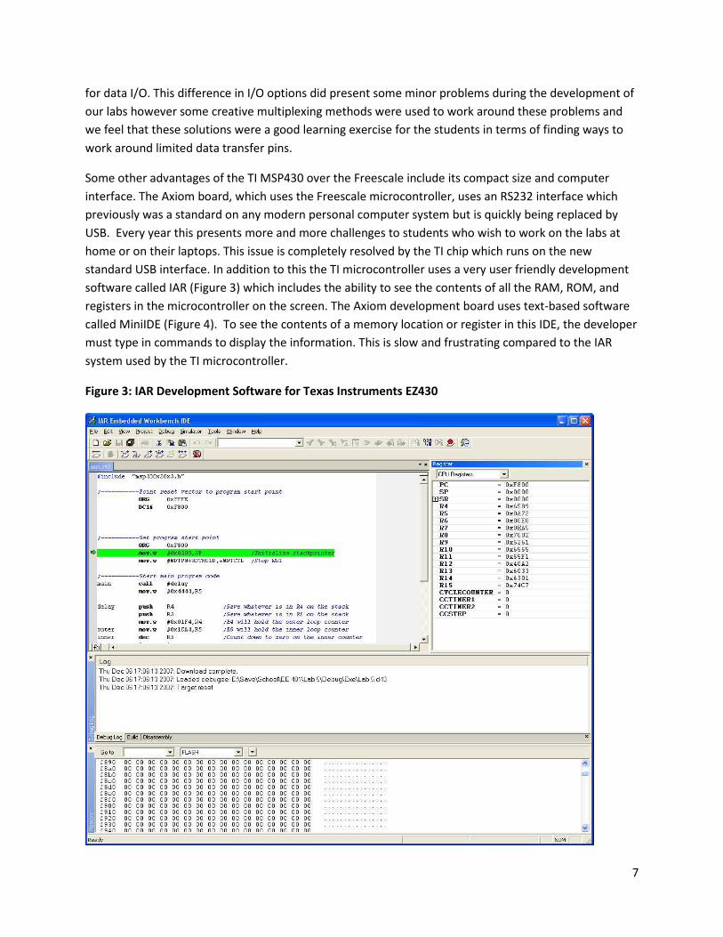
Some other advantages of the TI MSP430 over the Freescale include its compact size and computer
interface. The Axiom board, which uses the Freescale microcontroller, uses an RS232 interface which
previously was a standard on any modern personal computer system but is quickly being replaced by
USB. Every year this presents more and more challenges to students who wish to work on the labs at
home or on their laptops. This issue is completely resolved by the TI chip which runs on the new
standard USB interface. In addition to this the TI microcontroller uses a very user friendly development
software called IAR (Figure 3) which includes the ability to see the contents of all the RAM, ROM, and
registers in the microcontroller on the screen. The Axiom development board uses text-based software
called MiniIDE (Figure 4). To see the contents of a memory location or register in this IDE, the developer
must type in commands to display the information. This is slow and frustrating compared to the IAR
system used by the TI microcontroller.
Figure 3: IAR Development Software for Texas Instruments EZ430

8
Figure 4: MiniIDE Development Software for the Axiom/Freescale MC9S12C322
The largest advantage the Texas Instruments microcontroller has over the Axiom microcontroller for use
in education is cost. The EZ430 development kit shown in Figure 2 has a retail price of only $20 vs. $80
for the Axiom / Freescale kit shown in Figure 1. This cost difference is significant considering the rising
costs of education. A change in microcontroller for the ECE 251 course will save the students money
while enhancing the quality of their education.

9
Chapter IV – Lab Development
As mentioned previously in this report one of the biggest components of our project was to revise and
compose the labs to be completed by the volunteer group of students using the TI MSP430
microcontroller. One of our goals was to make the new lab tasks as similar as possible to the ones
completed by the rest of the students in the course using the Freescale microcontroller. Miguel Morales
started this process during the 2007 spring semester and completed several labs that we then revised
(see Chapter II). The students in both groups were required to complete all 8 MSP430 labs and 2
practical exams in lab using the MSP430. We wrote practical exams that would provide an almost exact
test of the students’ knowledge compared to the preexisting practical exams.
Another requirement of our project was to oversee the test students’ progress in the labs using just the
MSP430. We then incorporated their comments/suggestions about how to improve the labs. This set
up would be used as a way to judge whether or not the MSP430 could be used as an effective
educational tool for ECE 251. Each of us had a weekly lab session in which the students would come and
work on the labs, demonstrate completion of the labs and complete practical exams. We were in charge
of their grades for the course as well. Since Dr. Eads did not cover the instruction set for the MSP430 in
class, we were required to teach the students how to use the MSP430.
Table 2 shows a list of the labs the students were required to complete along with in which appendix the
lab document can be found. Following the table is a brief overview of each lab with the exception of
labs 1 and 2 which are review and introductory material that do not include material from either the
Freescale or TI microcontrollers.
Table 2: Completed Labs
Lab Number Lab Title Appendix Author
Lab 3 Hardware and Software Setup A Daniel/Miguel
Lab 4 Addressing Modes and Branching B Jeremy
Lab 5 Subroutines and The Stack C Daniel
Lab 6 Binary Coded Decimal Math D Jesse
Lab 7 Parallel I/O and Keyboard Scanning E Jesse/Miguel
Lab 8 Maskable Interrupts F Jeremy/Miguel
Lab 9 Input Capture and Output Compare G Daniel/Miguel
Lab 10 Analog to Digital Converter H Jesse/Jeremy
10
Lab 3 – Hardware and Software Setup
Lab 3 is a short basic lab that introduces the students to the process of installing the EZ430 drivers and
the IAR development software on a computer. The students are first walked through the process of
installing the drivers and software on a windows based computer. They then setup a project in the IAR
software, compile a test program and load it onto their EZ430 chip. The students are then introduced to
the basic tools in the IAR development tool including monitoring the progress of the test program,
seeing how it works on the actual hardware, and debugging any problems in the code.
Lab 4 – Addressing Modes and Branching
This lab covers the basics of memory addressing and program branching with the MSP430. The
requirements of this lab include basic hexadecimal math as well as modification of an existing program.
The program that must be modified contains a variety of addressing modes and branching techniques to
help the students become accustomed to their usage without the need to determine where to use each
type in a program. The student is also required to complete a set of questions about the result of simple
move operations using different addressing methods. Lab 4 also covers an introduction to some of the
basic assembler directives which are used with the MSP430.
Lab 5 – Subroutines and the Stack
In this lab the students are introduced to subroutines, which are used to break the program code into
manageable and repeatable sections. The stack is a memory management method that simplifies the
passing of data between subroutines and other programs within the system. The students are also
introduced to using the known time it takes to complete a specific instruction based on the operating
speed of the microcontroller to code a software delay, or a pause, in the execution of the program. This
is done by forcing the processor to complete a set number of empty program loops that do nothing but
keep it busy for a while. The students are then asked to write a program that could be used to control a
robot on a manufacturing line (a very simplified version of one anyway) that uses a subroutine to turn
on and off a paint nozzle with different colors and different delays between each coat of paint.
Lab 6 – Binary Coded Decimal (BCD) Math
Lab 6 introduces the students to working with binary coded decimal (BCD) mathematics including
addition, subtraction, multiplication and division. BCD is the representation of base 10 numbers only
using the first 10 hexadecimal numbers (0-9). The microprocessor is based on a base 16 system so that
all calculations done in hardware are in base 16. The students learn how to use special instructions with
the MSP430 so that they can do arithmetic decimally rather than hexadecimally. These instructions
work for addition and subtraction, but not for multiplication and division. For these, the students used
provided multiplication and division subroutines and wrote binary-to-BCD and BCD-to-binary programs
to perform the assigned arithmetic. First, the students would convert the numbers from decimal (BCD)
to binary, perform the arithmetic and then convert back to BCD.
Lab 7 – Parallel I/O and Keyboard Scanning

11
This lab introduces the students to Digital Input/Output (I/O) with the MSP430 and some basic polling
methods. The students must learn how to read in external digital signals to the microcontroller, execute
a program that interprets the input signal, decides what action is necessary and finally outputs a signal
to external hardware. The students first read in inputs from a dual-in-line package (DIP) switch and
output either a low or high voltage digital logic signal to an LED. The students then must implement
software that interprets signals from several different switches and lights up an LED if exactly the right
combination is given. Finally, the students must interface to a sixteen button keyboard. Using polling
(constantly checking the signal), their program must find which hexadecimal key was pressed and be
intelligent enough to know when the key has been depressed before registering another key being
pressed.
Lab 8 – Maskable Interrupts
The purpose of this lab is to introduce students to the usage of maskable interrupts as well as the use of
the timer system on the microcontroller. The first requirement of this lab is to extend the last
requirement of lab 7 to make use of interrupts instead of polling. This helps ease the students into the
use of interrupts in a familiar environment. The second requirement of this lab is to create a binary
clock which counts in 4 second intervals (4 LEDs to count seconds in a minute and 2 LEDs to count
minutes). This task requires the use of the MSP430 timer module and associated maskable interrupts.
The students are also required to receive inputs to start, stop and reset the timer. Lab 8 is particularly
important to the students as the majority of real-world microcontroller applications make extensive use
of timers and interrupts.
Lab 9 – Input Capture and Output Compare
One of the powerful tools included in most microcontrollers is the ability to gather data through
incoming signals and or output data to other devices. One method this is done is using a timer system
alongside input/output hardware to analyze and produce digital signals. The TI MSP430 does this
through its input capture and output compare hardware. The input capture looks at an incoming digital
signal and looks for rising or falling edges. The edges trigger events in the timer system so a program can
be written to analyze the timer information and decode the incoming data. The same is true in reverse
of the output compare system, the timer system is used to create the correct delays and then the
output pin is switched between high and low voltages to create a digital signal. In this lab the students
are asked to write several programs to analyze incoming signals and save the correct information in
memory.
Lab 10 – Analog-to-Digital Converter
One of the most practical labs from the ECE 251 course is the analog-to-digital (A/D) converter lab. In
this lab, the students learn how program the A/D converter on board the MSP430. This analog
converter uses successive approximation to assign a digital value to an analog signal. For lab 10, the
students were to take in a voltage signal from a power supply anywhere from 0-3.6V and output that
value to a 2-digit 7-segment display. Essentially, the students created a digital voltmeter. The MSP430
USB interface provides 3.6V to the chip, so anything over this value would not be acceptable for proper

12
operation. We were not sure about how much this value varied or how accurate the A/D converter was
because the display was typically within ±0.2 V whereas we would prefer strictly ±0.1 V for a margin of
error. This is something we will investigate more in our second semester project.
Practical Exams
There are two practical exams which cover the lab material taught throughout the semester. The first
exam covers material up to and including lab 6 while the second covers the remaining 4 lab assignments.
The purpose of these is to allow the students to demonstrate the skills they have learned as well as
show that they can work effectively under a time constraint. Practical Exam 1 requires students to use
subroutines and manipulate bits in memory. The student has the option to either pass the information
to the subroutine by value in a register for a lower point value or passing by reference on the stack for
maximum points. The second exam requires students to use a timer system along with I/O to begin an 8
second count when an input is set true and light an external LED when the time is completed. To get full
point for this exam the student must then configure the system to reset to the start state when the
input is set back to false.

13
Chapter V – Obstacles and Resolutions
One of the biggest challenges of this project was working with the ECE 251 students. Each of our group
members had no prior experience as a teaching assistant. This inexperience led to some problems with
the labs. There were several instances in which the students would misinterpret information from one
of us. There were also times when the students would be unclear about what they were required to
complete for the lab sessions. An example of how we attempted to resolve this is shown in Figure 5.
Usually the course has a single teaching assistant, so being consistent among 3 different people was also
a challenge. We did not compose all of the lab assignments before the semester started. Therefore, as
the semester progressed we learned to explain better what was required for each lab and attempted to
be clearer about how to use the MSP430 microcontroller.
Figure 5: Deliverables Section from Lab 9
Some of the other challenges that we faced included unforeseen differences between the MC9S12C32
and the MSP430 microcontrollers. One of the biggest components of the MC9S12C32 lab set involved
the functionality to output to the screen and take inputs from the computer’s keyboard. Since the
MSP430 does not have this capability, we defined a different focus for lab 4. In lab 4, the students were
to write an elevator program that either went up or down to a floor specified by a keyboard input. The
elevator would be shown on the screen including messages such as “going up” or “going down.” For lab
4, we focused more on the major concept of the lab, addressing modes. Next, we faced a problem when
trying to write lab 6, binary-coded decimal (BCD) math. The algorithm for converting regular binary-to-
BCD requires a multiplier and divider. However, unlike the MC9S12C32, the MSP430 does not have the
functionality to complete this type of arithmetic natively. Therefore we decided to provide subroutines

14
to complete these tasks. The students had varying degrees of success using these subroutines, and in
fact, some decided to write their own subroutines.
Another issue that we faced in this project was that the timer on the MSP430 was not as accurate as we
expected. We were not able to complete the tasks nearly as accurately as with the MC9S12C32. After
further research, we found a way to increase the accuracy, although not before the students completed
lab 9. One other major issue that we faced was that we did not have enough parallel I/O ports with
which to work. When interfacing with drivers and other external hardware, we did not have as much
flexibility as we would have liked. For lab 10 this meant having to be creative when using the I/O ports
when interfacing with the BCD to 7-segment display driver. A final issue that we faced was that the USB
tool required a driver that could only be installed by a privileged user. This would not be an issue except
for the fact that we do not have software installation privileges as is common in an education
environment. This limited students to a single university computer or their laptop to complete the labs.
At times we had to ask other students to move just so that we could complete the labs. However, we
found out that TI has released a new driver which resolves this concern. We would definitely
recommend using this new driver if the course does eventually switch to the MSP430.
There were several positive aspects for the project this semester. One of the biggest advantages to our
group of this phase of the project was that the development and teaching of these labs helped us learn
how to use the microcontroller. Another point of interest is that Rice University is interested in our labs
to be used for one of their microcontroller classes. The microcontroller has not been previously used in
education, so seeing interest in our work was definitely a positive result of the project. However, there
is still not a comprehensive textbook covering the use of the MSP430. Another significant setback is that
an adopting professor would have to write all new lecture notes for the course. Considering these two
major issues with the MSP430, we do not expect that our labs will be used soon by our university.
However, completing the labs gives the option to switch if the ECE department decides that this is the
best for the course.
Finally, we were concerned that the students who volunteered to complete the MSP430 labs would
have a disadvantage when it came to their understanding of the regular coursework. The students were
responsible for both microcontrollers including different functionality and instruction sets. Dr. Eads is
planning on adjusting their final grades to accommodate this problem. We feel that if the students did
not do well or fell behind it was partly due to the fact they were required to learn how to use both
microcontrollers. However, the most likely cause of the problem is that the course (as any current ECE
undergraduate would testify) is one of the most challenging and time-consuming lower level courses in
the ECE curriculum.

15
Chapter VI – Conclusions on completed work
This semester began with the goal of developing a set of labs for the ECE 251 microcontrollers course
which would be complete and ready to be performed by students. This set of labs was to utilize the new
TI-MSP430 F2012 microcontroller in the place of the existing Freescale MC9S12C32 microcontroller. To
help us determine if we met these goals we substituted our new labs for the Freescale labs for a
volunteer group of students. This allowed us to verify that the lab documents were of a high enough
quality and contained detailed enough explanation to allow the students to complete them as they
would the labs in the current course. Through this we discovered that the students were able to
successfully complete the lab assignments with minimal assistance which verified that they were
complete enough to be used in a classroom setting.
The original purpose of this project was to show that the TI-MSP430 would provide a better educational
tool than the currently in use Freescale MC9S12C32. There were four categories which we looked at in
an attempt to determine the best solution; cost to students, ease of use, viability for long term use and
capabilities relevant to education. The MSP430 was superior in cost to the students in that it is $60 less
expensive than the Freescale model. TI's controller was also found to be more intuitive and simple to
use for the students by providing a more user-friendly graphical interface and many diagnostic tools. Its
RISC architecture also made it easier for students to learn the full functionality of the instruction set.
The MSP430 is also a better long term solution as it interfaces with the computer via a modern USB
interface instead of the MC9S12C32's RS232 interface which is beginning to be excluded from modern
computer systems. The only category which was not a clear win for the MSP430 was capabilities
relevant to education; the Freescale controller includes a keyboard/terminal interface to the board
which is not duplicated by TI's controller. This, however, can be overcome with the extensive diagnostic
tools provided by the MSP430 developing environment.
Our conclusion after our first semester of work is that the MSP430 would make an excellent educational
tool. There is however one limiting factor which will stop the new controller from being adopted by CSU
in the short term: the fact that there is not currently a textbook associated with the MSP430. Therefore
any adopting professor would be forced to provide the students with an extensive set of notes to be
able to successfully teach the course. When a textbook is completed for this controller, it will make a
very capable and worthy addition to any ECE curriculum. We will enjoy using it in the continuation of
our design project next semester.

16
Chapter VII – Future Plans
The second semester of our project will be essentially a completely new effort as the first half has been
completed and has no logical continuation. The next phase of the project will utilize our experience with
the MSP430 from the first semester in the design of a self-setting clock. The microcontroller has many
features which make it a good candidate for this task. These features include low power consumption,
compact design and ample functionality to provide us with all of the I/O and processing capabilities we
need. This design will make use of several ECE concepts including analog circuit design, communications
and extensive use of microcontrollers. The combination of the practical clock design and the integration
of the functionality of the MSP430 microcontroller make this project a good continuation of the past
semesters work. The design will be divided into the following parts:
Receiver
An analog circuit designed to receive the 60kHz signal broadcast from the WWVB radio signal in Ft.
Collins. We are currently reviewing several possible designs for this circuit. During the next semester
we will need to determine which design will best suit our needs then construct that circuit. A picture of
the WWVB radio station is given in Figure 6.
Figure 6 WWVB Radio Station [3]
Amplifier
An amplifier circuit will be required to ensure that the signal which is fed to the MSP430 has a range
between 0V and 3V.

17
Decoder
This will be take in the digital signal from the WWVB broadcast and determine the relevant data that it
contains. The signal is shown in Figure 7. The decoder will find the values for the minutes, hours and
day and save them for use in other parts of the design.
Figure 7 WWVB Time Code Format [4]
Clock
The MSP430 will also be used to keep a running clock to allow the time to stay updated even when the
signal is not being synchronized to the WWVB signal. This clock will have to receive inputs to allow
manual setting of the clock (along with disabling the automatic setting feature) and time-zone
adjustments to create a more robust design.
Display
To make the clock useful it must have a display to show the current time information. We plan to use an
LCD. We will first use an inexpensive display to use for diagnostic purposes and then obtain a more
sophisticated display to use in the final product.
Optional Extensions
We have purposely limited the scope of our second semester project to ensure that we can complete it
in our single semester time frame. However there are several extension options should the main design
be completed ahead of schedule. We have determined the following three possible additions to our
project.
Solar power Generation
This would allow the clock to run without an external power source and involve the use of solar cells, a
battery charger and a battery to provide power during dark hours.
Alarm Capabilities
One of the leading benefits of a self setting clock is to provide a highly accurate time signal to whichever
device it is hooked to. A natural extension of this is to add alarm capabilities to provide a reliable
notification of when a time has been reached. This would require an added external input to adjust
alarm time settings along with a speaker to provide a notification to the user.

18
Temperature Sensing
We have discovered that the MSP430 has temperature sensing capabilities built in. If we can verify that
these sensors have adequate accuracy and reliability we could incorporate temperature reading into our
clock design. There is also an RF version of the MSP430 which could allow this same functionality but
from a remote wireless sensor. Both of these possible additions would require the MSP430 to operate
as a thermometer in addition to the current requirements. The microcontroller would also have to
output more information to the screen.
A Gantt chart for next semester’s work is given in Figure 8 below.
Figure 8 Project Timeline Gantt Chart

19
References
[1] Axiom Manufacturing, “CML-12C32,” [Online document], [cited 2007 Dec 6], Available HTTP:
http://axman.com/?q=node/46
[2] Texas Instruments Incorporated, “eZ430-MSP430F2013 Development Tool User’s Guide,” pp 5.
[Online document], [cited 2007 Dec 6], Available HTTP:
http://focus.ti.com/lit/ug/slau176b/slau176b.pdf
[3] National Institute of Science and Technology,“NIST Radio Station WWVB,” [Online document],
[cited 2007 Dec 6], Available HTTP: http://tf.nist.gov/stations/wwvb.htm
[4] Wikimedia Foundation, Inc. , “WWVB Modulation Format.” [Online document], [cited 2007 Dec
5], Available HTTP: http://en.wikipedia.org/wiki/WWVB
[5] Texas Instruments Incorporated, “MSP430x2xx Family User’s Guide.” pp 3-75. [Online
document], [cited 2007 Dec 4], Available HTTP:
http://focus.ti.com/lit/ug/slau144d/slau144d.pdf.

20
Bibliography
[1] “Lab 1: Review of Digital Circuit Logic.” (for use with Freescale MC9S12C32) Fort Collins, CO.
Colorado State University, 2005.
[2] “Lab 2: Timing Measurements, Fan-Out & Digital to Analog Interface.” (for use with Freescale
MC9S12C32) Fort Collins, CO. Colorado State University, 2005.
[3] “Lab 3: Software Setup and Introductory Programs.” (for use with Freescale MC9S12C32) Fort
Collins, CO. Colorado State University, 2005.
[4] “Lab 4: Addressing Modes and Branching.” (for use with Freescale MC9S12C32) Fort Collins, CO.
Colorado State University, 2005.
[5] “Lab 5: Subroutines and the Stack.” (for use with Freescale MC9S12C32) Fort Collins, CO.
Colorado State University, 2005.
[6] “Lab 6: BCD Multiplication and Division.” (for use with Freescale MC9S12C32) Fort Collins, CO.
Colorado State University, 2005.
[7] “Lab 7: Parallel I/O and Keyboard Scanning.” (for use with Freescale MC9S12C32) Fort Collins,
CO. Colorado State University, 2005.
[8] “Lab 8: Timing Maskable Interrupts.” (for use with Freescale MC9S12C32) Fort Collins, CO.
Colorado State University, 2005.
[9] “Lab 9: Input Capture and Output Compare.” (for use with Freescale MC9S12C32) Fort Collins,
CO. Colorado State University, 2005.
[10] “Lab 10: Analog-to-Digital Converter.” (for use with Freescale MC9S12C32) Fort Collins, CO.
Colorado State University, 2005.
[11] Texas Instruments Incorporated, “MSP430x2xx Family Data Sheet.” [Online document], [cited
2007 Dec 4], Available HTTP: http://focus.ti.com/lit/ds/symlink/msp430f2012.pdf

21
Acknowledgements
We would like to thanks Texas Instruments for the hardware donations including MSP430 USB kits with
for the F2013 device, kits of MSP430F2012 target boards and hardware development starter kits. We
estimate the approximate value for their donations to be around $700 total. Without their generous
donations running the labs and learning how to use the processors would not be possible. We would
also like to thank Miguel Morales who started this project during the spring 2007 semester. He has
provided us with guidance and assistance in the project and has been generous with his time. Finally,
we would like to thank Dr. Bill Eads, our project advisor. Dr. Eads always had a very sensible and
practical perspective on our project goals and progress. We appreciate the offer of his time and
expertise considering that he is not paid like a full time faculty member.
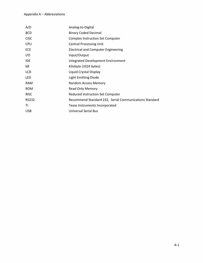
Appendix A – Abbreviations
A-1
A/D Analog-to-Digital
BCD Binary Coded Decimal
CISC Complex Instruction Set Computer
CPU Central Processing Unit
ECE Electrical and Computer Engineering
I/O Input/Output
IDE Integrated Development Environment
kB Kilobyte (1024 bytes)
LCD Liquid Crystal Display
LED Light Emitting Diode
RAM Random Access Memory
ROM Read Only Memory
RISC Reduced Instruction Set Computer
RS232 Recommend Standard 232, Serial Communications Standard
TI Texas Instruments Incorporated
USB Universal Serial Bus

Appendix B – Budget
B-1
This semester we have not incurred any costs from our allowed budget of $300 dollars ($50 per person
per semester). We will be spending this allowed budget next semester on clock chips, receiver chips,
printed circuit boards, displays and other required hardware.
A breakdown of the donations we have received so far this semester is shown below.
12 MSP430 USB kits with F2013 device @ approx. $20 each (donated by TI)
15 kits of 3 MSP430F2012 target boards @ approx. $10 each (donated by TI)
2 Hardware Development Starter kits @ approx. $150 each (donated by TI)
Total Donations approx. $700 (from Texas Instruments Inc.)

Appendix C – Lab 3
C-1
3.1 – Objectives This introductory lab will walk you through the process of creating an assembly project, assembling a program, downloading it to the EZ430 (the development kit for the TI-MSP430F2012) and executing / debugging the program. When you complete this lab, you should be able to:
- Understand the IAR Embedded Workbench IDE. - Assemble (build) a program using the IAR Embedded Workbench. - Download a program onto your EZ430. - Run a program and examine memory registers. - Use stepping and breakpoints to debug the program.
Because you will perform all of these procedures in every lab you do after this, a complete understanding of the material in this lab is necessary. 3.2 – Reading Material You will need to read the following introduction material prior to completing this lab, all are available on the ECE 251 website.
I. Introduction to the MSP430-F2012 controller II. Introduction to assembly programming III. MSP430 Instruction Reference Sheet
3.3. – Hardware / Software Startup The computers in the microprocessors lab will have the correct drivers and IAR software preinstalled for you. For installation on your home computer please refer to the EZ430 user guide which is available on the ECE 251 website.
Software Setup & Introductory Assembly Programs
3

Appendix C – Lab 3
C-2
3.4 – Introduction to the IAR Embedded Workbench IDE
Invoke the IAR Embedded Workbench in one of the following two ways:
1. Left click your mouse on the START menu on the bottom left of your screen. Then follow the path, Programs � IAR Systems � IAR Embedded Workbench Kickstart for MSP430 V3 � IAR Embedded Workbench.
2. Open Windows explorer and locate IAR Embedded Workbench.exe in the folder
C:\Program Files\IAR Systems\Embedded Workbench 4.0\common\bin\IarIdePm.exe To create the shortcut on your desktop, right click the mouse on IarIdePm.exe and then left click on create shortcut. Then click on this shortcut to invoke the IAR Embedded Workbench application. This part of the lab is considered the tutorial that will be repeated for your TA: Step 1 – Creating a Project The first thing you will see is the Embedded Workbench Startup screen. This screen will be a good shortcut to open existing workspaces and create new projects in the future, but for now, click the Cancel button. Note that a workspace can hold one or more projects, each which can hold groups of source files (the files that contain your assembly code). Click on File -> New -> Workspace. This opens a new workspace in which to place your projects. You must always open a workspace before you can create a new project. To create a new project, click Project -> Create New Project… The Create New Project box will appear. IAR lets you choose whether you want to create an assembly (asm), C, or C++ project. Expand the asm tab and click OK once you have selected the asm option.
Appendix C – Lab 3
C-3
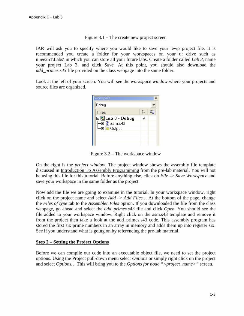
Figure 3.1 – The create new project screen IAR will ask you to specify where you would like to save your .ewp project file. It is recommended you create a folder for your workspaces on your u: drive such as u:\ee251\Labs\ in which you can store all your future labs. Create a folder called Lab 3, name your project Lab 3, and click Save. At this point, you should also download the add_primes.s43 file provided on the class webpage into the same folder. Look at the left of your screen. You will see the workspace window where your projects and source files are organized.
Figure 3.2 – The workspace window On the right is the project window. The project window shows the assembly file template discussed in Introduction To Assembly Programming from the pre-lab material. You will not be using this file for this tutorial. Before anything else, click on File -> Save Workspace and save your workspace in the same folder as the project. Now add the file we are going to examine in the tutorial. In your workspace window, right click on the project name and select Add -> Add Files… At the bottom of the page, change the Files of type tab to the Assembler Files option. If you downloaded the file from the class webpage, go ahead and select the add_primes.s43 file and click Open. You should see the file added to your workspace window. Right click on the asm.s43 template and remove it from the project then take a look at the add_primes.s43 code. This assembly program has stored the first six prime numbers in an array in memory and adds them up into register six. See if you understand what is going on by referencing the pre-lab material. Step 2 – Setting the Project Options Before we can compile our code into an executable object file, we need to set the project options. Using the Project pull-down menu select Options or simply right click on the project and select Options… This will bring you to the Options for node “<project_name>” screen.

Appendix C – Lab 3
C-4
Figure 3.3 – The project options screen
- In the General Options menu:
• Set the Device to the MSP430F2012 - In the Debugger menu:
• Set the Driver to FET Debugger. This makes sure that once compiled into an object file, the program will be loaded onto your physical microcontroller, not the IAR simulator.
• If you would ever like to work on your code but you do not have your EZ430, you can set the Driver option to Simulator and the IAR Embedded Workbench will simulate your microcontroller.
- Under the actual FET Debugger menu:
• Change the Connection from LPT -> LPT1 to TI USB FET. This tells IAR to look for your USB stick and not a port on your computer.
• Change the Target VCC option at the bottom of the screen to 3.0 - Click OK to finalize your settings. You are now ready to build and compile your
project. Step 3 – Running the Program Before we compile the project, make sure to save your project to preserve its settings. Select the add_primes.s43 file in the workspace window and click Project -> Compile. Alternatively, you can right click on the source file and select Compile. When the workbench is finished compiling your source code, you will see a new window at the bottom of the

Appendix C – Lab 3
C-5
screen called your Build Messages Window. It should say that there are 0 errors and 0 warnings.
Figure 3.4 – The build message window
To see what happens when your code contains an error, erase one of the semicolons preceding a comment in the add_primes.s43 code and re-compile. The build message window displays:
- Any errors/warnings in your code - The assembler’s best attempts of an explanation - The name of the files in which the errors/warnings occurred - The line number where the errors/warnings occurred
Double click the line that says “Error[0]: Invalid syntax.” In the file, your cursor will be placed close to the location of the error. Fix the error, and then re-compile. Now make sure that your EZ430 is plugged in and click Project -> Debug. This will run your code on the EZ430 and put you in debugging mode. Step 4 – Debugging A Project A new window has been added to the screen in debugging mode. It is called the Disassembly Window. After the assembler compiles your code into machine code, a disassembler program does the opposite and creates the contents of the disassembly window. You can apply the debugging commands to either the coded assembly file or the disassembly window. Generally, this tool is more useful when the developer has written his/her application using the C programming language and wants to see how the machine interpreted his/her code in assembly. The workbench allows users to move and dock windows as they wish. To see this, click View -> Memory and View -> Registers. Click on the window labels to drag and dock them in the same tab group as the Debug Log and Build windows. These windows are updated as the program executes, giving the user extremely useful insight to the inner workings of his/her program.

Appendix C – Lab 3
C-6
NOTE: If the contents of the window selected in each tab group ever change, the changed contents will be highlighted red to show the change. The Memory Window The memory window allows the user to navigate the entire memory map of the MSP430. Since we used assembler directives to load the array of prime numbers starting at memory location 0200h, type 0x0200 into the Go to box. You will see the array stored in consecutive words in memory.
Figure 3.5 – The memory window
Instead of Memory, IAR also gives you the option to looking at:
- SFR: The special function and peripheral registers - RAM: Memory - INFO: Information FLASH memory (ROM) - FLASH: Main FLASH memory (ROM)
NOTE_01: You can use the information and main memories just the same. The only difference is how the memory is physically segmented and the address. NOTE_02: If you look at the FLASH memory, notice that this is where the main program is stored. The numbers you see are the instructions of the program that have been stored for program execution. The Register Window The register window shows the user any of the important registers whether they be peripheral control registers, special function registers, or just the basic CPU registers. For the most part, you will only be interested in the CPU Registers, but know that the other registers are available for viewing. Also note that the Status Register (SR) containing the status bits can be expanded to see each individually labeled bit. While stepping through the program, periodically check the Memory and Register windows to see how they change according to your code.

Appendix C – Lab 3
C-7
Inspecting Source Statements Run your mouse over these buttons in the top left corner of your debugging session and read their function in the bottom left corner of the IAR workbench frame.
Figure 3.6 – The debugging buttons
Program Reset Resets the execution of your program. Takes you back to the instruction address located in the reset interrupt vector.
Step Over Steps over the current step point.
Step Into When you debug a program with subroutines in assembly, you can choose to “Step Over” the subroutines, meaning that the subroutine is executed but you don’t step through it in the debugger, or you can choose to “Step Into” the subroutine. Stepping into a subroutine will allow the user to see the individual op-codes executed.
Step Out Of If you have stepped into a subroutine, steps out of the subroutine and to the next instruction after the subroutine call.
Step to the Next Steps to the next statement, regardless of the circumstances. Statement
Execute to the Executes the program to the line at which the cursor is Current Cursor currently located. Position
Run Runs the program straight through or until a breakpoint.
Stop Debugging Stops the debugging session returns the user to programming mode.
At the top right-hand side of the page, note this button as well:
Make and Reset Press when code has been modified so that it needs to be re-compiled and the debugger needs to be reset

Appendix C – Lab 3
C-8
Breakpoints Sometimes it is beneficial, if you want to know how your program is executing at a certain point in its execution, to use breakpoints. To place a breakpoint in the program, double click on the margin next to the line at which you wish to set a breakpoint (or right click on the line and select toggle breakpoint (conditional)). For example, the initial operators in every assembly code project that initialize the controller after a Power Up Clear can often be assumed to work properly. If you would like to run the program starting immediately after this section of code, add a breakpoint at the line labeled main. Since we have two clear operators in the beginning of our code that we know will work, place a breakpoint at the first mov.w instruction line of the main program. Press the Program Reset button to restart program execution and then press the Run to execute until the breakpoint. From here on, play with the other buttons to gain some intuition as to their function. NOTE: Debugging can also be done in the disassembly window. Try it out and see if you can follow what all the numbers mean in regards to the CPU registers and memory. For more information on debugging, reference the EZ430_UserGuide. An in-depth understanding of the debugging module is a truly powerful tool for future programming. After completing this tutorial, you should feel comfortable working with the IAR Embedded Workbench. If you do not, you may want to go back and do it again. Also, make sure you have read and understand the material from lab section 3.2. It will be critical to the execution of future labs.
3.5 – Procedure 1. Set up the EZ430, IAR Embedded Workbench, and all necessary hardware. 2. Complete the tutorial. Call the lab TA and repeat the tutorial in their presence, without reading the directions. When you can do this without looking at the instructions, the TA will check you off. Review any part of this lab you are not sure about. 3.6 – Questions
1. Describe the register set for the MSP430F2012. What are the Special Function Registers (SFRs) and their functions? Where are they located?
2. How are single stepping and breakpoints used to debug a program? Why might you use
breakpoints rather than single stepping? 3. In the Disassembler window, what do the numbers on the far left mean? What does this
have to do with the contents in R0 during program execution?

Appendix C – Lab 3
C-9
3.7. – Lab Report The lab report is due at the beginning of the next lab. For the lab write up, include the following:
1. Your marked up version of this document. 2. A brief discussion of the objectives of the lab and the procedures performed in the lab. 3. Answer to any questions in the discussion, procedure or question sections of the lab.

Appendix D – Lab 4
D-1
4.1 - Objectives
The MSP430 offers 7 different methods of forming an effective address to determine the location of data to be used in an instruction. When you complete this lab you should be able to do each of the following:
• Write programs to address memory in each of the different addressing modes.
• Use the assembler directives.
• Write simple assembly programs to perform multi-byte addition and subtraction.
• Use the status flags with conditional jump instructions.
• Mask and test individual bits using logical AND and OR instructions.
4.2 – Related material to read
• MSP430 Addressing Modes: Section 3.3 in the MSP430x2xx Users Guide, pages 3-9 to 3-16
• Program Loops: Section 2.5.3 in Intro to Assembly
• Assembler Directives: Section 2.4 in Intro to Assembly
• Instruction Reference: Listed under “Reference Material” on the website
Addressing Modes and Branching
4

Appendix D – Lab 4
D-2
4.3 – Addressing modes
When the microcontroller executes an instruction to access memory, it forms an effective address. Instructions can tell the microcontroller to form the address in different ways. These are called addressing modes. The MSP430 uses seven different addressing modes. Due to its completely orthogonal architecture, all addressing modes can be used with any instruction for this controller. This offers a great deal of flexibility, particularly if you have a solid understanding of the different addressing modes. The first addressing mode we will cover is register addressing mode. This mode uses the contents of the register as the value for the operation. In the following example the contents of R8 will be added to the contents of R10.
add.w R8, R10
Next there is the immediate addressing mode. This mode is useful when you need to use a constant value for any reason during program execution. This addressing mode can not be used for the destination of a command. The following instruction will subtract 20 from the contents SP (the stack pointer) and place the result back in SP.
sub.w #20, SP
Note the ‘#’ symbol preceding the constant value; this indicates that the instruction will use the immediate addressing mode.
Similar to immediate addressing is the absolute addressing mode. In this case the value which is used in the instruction is the literal address in memory which stores the data used in the operation. The following instruction will move the value stored at 0x0400 to 0x500.
mov.w &0x0400, &0x0500
Note the ‘&’ symbol which indicates that the value 0x0400 is a location in memory which stores the data for the operation.
Another method of forming an effective address is the indexed addressing mode. In this mode the contents of the register form a base for calculating a pointer to the address which will be used by the instruction. An index is then added to this number and the sum is the location in memory which holds the data which is to be used. In the following example assume that R5 holds the value 0x5000 and R9 holds the value 0x9000, the following instruction will move the value stored at 0x5008 to 0x9004.
mov.w 8(R5), 4(R9)
Next we will discuss the indirect addressing mode. This mode treats the contents of a register as a pointer to the address containing the data to be used in the operation. This is the same as using indexed addressing as above, except with an argument of 0 (e.g.

Appendix D – Lab 4
D-3
0(R5)). Indirect addressing can only be used for the source operand in an operation. The following example will load the value stored at 0x8000 into R11 (0x8000 is stored in R10).
Mov.w @R10, R11
Note the ‘@’ symbol is required to indicate that indirect addressing will be used.
Finally we have auto-increment indexed addressing. This method works the same as indexed addressing with the exception that it will increment the source register after completing the operation. This is useful for working with continuous data sets like you would find in a table as the register will already be pointing at the next location, ready for another operation. The following example will perform the same operation as the last example, the difference is that R10 will contain 0x8002 after the operation completes.
Mov.w @R10+, R11
4.4 - Assembler directives
Assembler directives are instructions in your program that are not executed by the processor; instead they are used by the compiler to give it additional information to be used when compiling your code. There are a few assembler directives we need to discuss before you start writing programs. These are also described in Intro to Assembly section 2.4. Figure 4.1 gives an example of how to use the common directives needed for this lab.
Example 4.1 is a simple program to create a table in memory, and then copy it to another location in memory. Line 1 uses the #include directive which is taken from the C programming language. This directive will import the msp430x20x3.h file and allow the program to use any of the methods or information contained in the imported file.
The Symbol Definitions section of the program is where values used in the program can be assigned to easy to remember names using the EQU directive. When the compiler sees EQU it replaces every other instance of the name (in this case offset) with the value (in this case 2Fh) and the controller will never see the name. This is very useful when you are going to use a value multiple times throughout a program. If a value ever needs to be changed, you will only need to change it once at the EQU statement and your whole program will be updated. It can also be useful to allow you to address values by a meaningful name to make the program more readable.
Next is the Data section of the program. This is used to allocate the memory which will be used during the execution of the program. The ORG directive tells the compiler that the following data will be stored starting at memory location 0x0200. This is necessary to let the compiler know where to place different portions of the program, such as the Data and Program sections. You will notice the ORG directive twice more, in the Interrupt Vectors section as well as in the Program section. Any data that is loaded into

Appendix D – Lab 4
D-4
specific areas of memory must have an ORG directive to tell the compiler where it should be placed. Another directive used in this section is the DW directive (you can also use DC16), this directive defines a word of memory to the value which follows. There are also similar directives to define memory of different sizes; DB (or DC8) defines a byte in memory, DL (or DC32) defines 32 bits and DC64 defines 64 bits in memory.
In the Interrupt Vectors section, the ORG and DW directives are used once more. In this case the DW directive defines the memory to an address instead of a constant, this is used to define the location in memory at which the program will program will begin running.
The program section includes the END directive. This signals the compiler that there is nothing after this point in the file. Even if there were more operations following the END directive, the compiler would never see them and therefore they would not be executed.
#include "msp430x20x3.h" ;------------------------------------------------------------------------ ; Symbol Definitions ;------------------------------------------------------------------------ offset EQU 2Fh ;------------------------------------------------------------------------ ; Data ;------------------------------------------------------------------------ ORG 0x0200 first DW 0x0210 count DW 10h ;------------------------------------------------------------------------ ; Interrupt Vectors ;------------------------------------------------------------------------ ORG 0FFFEh DW StopWDT ; start running at StopWDT ;------------------------------------------------------------------------ ; Program ;------------------------------------------------------------------------ ORG 0xf800 StopWDT mov.w #WDTPW+WDTHOLD,&WDTCTL ; Stop Watchdog Timer start clr R4 ; set R4 to zero mov.w first, R5 ; set address of table in R5 mov.w count, R6 ; initialize loop counter in R6 loop1 mov.b R4, 0(R5) ; write values to initial table inc R4 ; update values and counters inc R5 dec R6 jne loop1 mov.w first, R5 ; reset R5 to first table mov.w count, R6 ; initialize loop counter in R6 loop2 mov.b @R5+, offset(R5) ; copy table value to new table dec R6 jne loop2 stop jmp stop ; keeps the program here END
Figure 4.1: This program is designed to introduce you to some of the basic assembler directives as well as an example of how to use different addressing modes effectively.

Appendix D – Lab 4
D-5
4.5 – Program Format
An important consideration when programming is writing your code in an easy to read format. In Figure 4.1 for example, the program is divided into 4 different labeled sections. While it is not necessary to precisely follow the above example, you should be conscious of the readability of your code. It is also important to comment your code appropriately. Well commented code is much easier to understand when you edit or debug it in the future.
4.6 – Branching
A very important concept in any type of programming is branching. Branching is what allows programs to have loops, conditional statements and many other frequently used structures. There are two fundamental types of branching in assembly; conditional or unconditional.
Unconditional branching acts just as the name suggests, no matter what the current state is when an unconditional branch instruction is reached, the program will jump to the location specified by the branch. On the MSP430, the instructions used for this type of branching are the BR and JMP commands.
Conditional branching is more complex and flexible. The conditions which determine the behavior of these instructions are in the status register (SR) of the controller. Depending on the instruction used, different bits of the SR will be used to determine whether or not to branch. The most common instructions you will likely use are JNE (or JNZ) which will jump if the Z bit of the SR is false (usually set if a mathematical operation resulted in a zero) and JEQ (or JZ) which will jump if the Z bit is true. There are many more of conditional branching instructions listed in the instruction reference sheet (or on page 3-20 of the MSP430x2xx Family Users Guide).
Figure 4.1 has examples of conditional branching in loop1 and loop2. In both of these, the loops will be repeated until the R6 is zero, then they will not branch and will continue executing the next instruction.
4.7 – Bit masking and packing
It is often useful to be able to look at individual bits instead of a whole byte or word when programming in assembly. To aid in this, the MSP430 has bitwise AND, OR, NOT and XOR instructions.
If you want to check if certain bits are true, you can AND the number with a binary number equal to the bits you wish to check. The following instruction would set all of the bits except 3 and 5 in R5 to zero; bits 3 and 5 would retain their values. This is called bit masking.
AND 0x0014, R5
Appendix D – Lab 4
D-6
If you use an OR operator in the same context as above, you would be setting bits 3 and 5 to 1 without changing any of the other bits. This is called bit packing.
OR 0x0014, R5
There may also be times when you need to test every bit of a register one at a time and branch based on the result. There are two rotate instructions RLC and RRC which can be used for this. RLC will rotate the bits in a register left through the carry bit C of SR which can then be used by the JNC or JC instructions which jump when C is 0 or when C is 1 respectively. The RRC instruction will rotate the bits right through the carry bit.
4.8 - Procedure
Before you come to the lab, you must do all the necessary calculations manually. You must also write programs for the following procedures before coming to lab. At the start of the lab, show the TA your results, programs, and flowcharts for all parts of the lab. Refer to the Flowchart Reference to understand the basics of how to write the flowcharts. Show the working programs to TA.
1. Manually calculate the results and write down the 'C' and 'Z' of the condition code register after performing the following additions and subtractions. Write programs to add or subtract the following numbers from memory and store the sum in memory. Use the DW instruction to initialize the memory locations. Execute the programs and record the sum or subtraction and the ‘C’ and ‘Z’ bits of the condition code register. Verify the results with your manual calculations and the value of the 'C' and 'Z' bits. Use the following data:
a. Addition of two double-byte numbers: C300h + 8D00h
b. Subtraction of two double-byte numbers: F500h – 3400h
c. Multi-byte addition: 2E68B3F4h + 5C2Ah
d. Multi-byte subtraction: FE6B34h - 58CF21h
2. Consider the program in Figure 4.1. Modify that program so that all the following changes are made in your new program:
a. The table to be copied is of length 20h.
b. The original table is created starting at 0x0220.
c. The table starts with 0 and successive even numbers are stored in the table.
d. The duplicate table is created starting at 0x0260.
e. The duplicate table contains the copy of the original table in the reverse order.
Show the results to the TA after running this modified program.

Appendix D – Lab 4
D-7
4.9 – Questions
1. Describe the function of the assembler directives: ORG, EQU, DW, DB and END.
2. If the following data is stored as described,
R4 = 0x1155
R5 = 0x0220
Memory Address 0x0250 = 1234h
Memory Address 0x0252 = ABCDh
What number is in R4 after each of the following instructions is executed? (Assume each instruction starts from the state shown above)
a. mov.w &0x0250, R4
b. mov.w 30h(R5), R4
c. mov.w #0x00FF, R4
d. mov.b &0x0253, R4 (Hint: it may be helpful to write a simple program to see how this works)
4.10 - Lab report
For the lab write up, include
1. Your marked up version of this document.
2. Flowcharts and programs that you wrote before the lab.
3. Manual results that you calculated before the lab.
4. A copy of your working .asm files.
5. A brief discussion of the objectives of the lab and the procedures performed in the lab.
6. Answers to any questions in the discussion, procedure, or question sections of the lab.
Appendix E – Lab 5
E-1
5.1 - Objectives
A subroutine is a reusable program module. A main program can call or jump to the subroutine one or more times. The stack is used in several ways when subroutines are called. In this lab you will learn:
• How to write subroutines and call them from the main program.
• Ways to pass parameters to and from subroutines.
• How to use the stack and the stack pointer.
• How to create and use software delays.
5.2 - Related material to read
• Review any previous lab readings as needed.
5.3 - Introduction
A subroutine is a program module that is separate from the main or calling program. Frequently the subroutine is called by the main program many times, but the code for the subroutine only needs to be written once. When a subroutine is called, program control is transferred from the main program to the subroutine. When the subroutine finishes executing, control is returned to the main program. The stack provides the means of connecting the subroutines to the main program. Subroutines can save memory as well as help organize your programs. In future labs, you will find it beneficial to use subroutines for various functions of your programs.
Subroutines and the Stack
5

Appendix E – Lab 5
E-2
5.4 - The Stack
The stack is actually just an area of memory whose highest address is stored in register R1 which is referred to as the stack pointer or SP. Make sure you understand the difference between the stack and the stack pointer. The stack is an area of memory; the stack pointer is the address of the last value pushed onto the stack. Usually, the stack is used for storing data when subroutines are called. It is a last-in-first-out, i.e., LIFO structure so the last thing stored in the stack is the first thing retrieved. A mechanical analogy will help you learn how the stack operates. One common mechanical stack is the plate rack used in some cafeterias (illustrated in Figure 5.1).
Figure 5.1: Plate and stack analogy to computer stack operation. (taken from ‘Microcomputer engineering by Miller’).
Figure 5.1(a) illustrates a cross-section of a plate rack containing some plates. As hungry consumers go through the cafeteria line, each person takes a plate off the top of the rack. When a plate is removed, a mechanism moves the plate upward so that the next plate is now at the top of the rack. Figures 5.1(b) and 5.1(c) illustrate this process. The next consumer now can easily access the next plate that is at the top of the rack. When the dishwasher puts clean plates into the rack, the mechanism moves downward. The top plate is again at the top of the rack, as Figure 5.1(d) illustrates. If you consider the usage of the plates, you see that the last plate put into the rack is the first plate removed from

Appendix E – Lab 5
E-3
the rack. Thus the dish rack is a last in first out or a LIFO device. The stack operates in exactly same way; hence it is also referred to as a LIFO data structure.
The push instruction copies the data in the specified register into RAM and then decrements the stack pointer by 2 bytes. The pop instruction works in the exact opposite way. To explain this in detail we will look step by step at a simple section of program code.
1 mov.w #0x0280,SP
2 clr R4
3 clr R5
4 mov.w #0x1122,R4
5 push R4
6 pop R5
Figure 5.2: Example stack code
The first line sets the stack pointer (which is R1 however we will always call it SP) to point at the highest byte in RAM 0x0280. The next two lines clear the registers R4 and R5 (meaning they now have all zeros). And the third line places the data 0x1122 into R4.
The fifth line uses the push instruction to push the bits in R4 onto the stack, this means that after this instruction the byte at address 0x027F will contain 0x0011 (note only 8 bits in a byte) and the byte at 0x027E will contain the byte 0x0022. Note that the push command decrements the SP by one byte BEFORE it copies the first byte from R4 onto the stack, this is why we point the SP at 0x0280 even though we cannot write data into the address 0x0280. After the push instruction the SP is now pointing at 0x027E meaning when the stack is not empty the SP points at the most recent byte added onto the stack.
The sixth line uses the pop instruction to pull the top word (16 bits) from the stack and place it in R5. The process works in reverse of the push instruction meaning the data 0x1122 is coped from the stack into R5 and the SP is incremented by 2 bytes and after the pop command the SP is again pointing at 0x0280. A good practice in your code is to make sure you have a pop for every push or you end up with data on your stack you may not mean to have there.
One of the primary uses for the stack is storing data when running a subroutine which brings us to the next topic of this lab.

Appendix E – Lab 5
E-4
5.5 - Subroutines
Subroutines are an extremely useful tool for any programmer that needs to execute the same sequence of instructions at different times during the operation of a program. This can be anything from a simple timer to the output of data or even a calculation of data. Subroutines are called using the call instruction. Recall that the program counter or PC always points to the location of the next piece of code to be executed thus if we jump out of the main program (or whatever routine we are in) into a subroutine we need to change the PC. The call instruction does this, it pushes the current PC onto the stack and then places the argument of the call instruction into the PC. For example the code “call 0xF900” would push whatever is in PC onto the stack and place 0xF900 into the PC thus causing the next instruction to be whatever is stored in the location 0xF900. Note that names can also be used instead of address as you will see in the examples. In fact the call instruction can be used with any addressing mode. At the end of the subroutine the ret instruction is used, this instruction pulls the saved PC location from the stack and places in back in the PC thus returning program flow to the previous routine (main or whatever routine called the subroutine) Note that a subroutine can call another and another so long as there is room on the stack to save the proper PC locations. Also keep in mind that if a subroutine uses any PUSH or POP instructions it MUST have one pop for every push or the ret instruction will not pull the correct PC location from the stack.
main call #sub1 sub1 mov.w #0x4444,R4
RET Figure 5.3: Simple example of a call and return
5.6 - Parameter passing
A parameter is passed to the subroutine by leaving the data in a register, or memory, and allowing the subroutine to use it. The subroutine can then change the data if needed and pass the parameter back to the calling program in the same way. When the parameter being passed to the subroutine is in a register, this is referred to as the call-by-value technique of passing parameters. If the data is in memory and the address is passed to the subroutine, this is called call-by-reference. It is important to document all parameter-passing details in subroutines. There are other tricky ways of passing data to a subroutine using the stack by pushing the data onto the stack before the call instruction is used, however the data cannot be pulled from the stack with a pop or the PC location put on the stack by the push will be lost. Therefore the data must be accessed on the stack by using the SP+2 or some such reference to a location in the stack OTHER than the current SP value. This technique can be useful but tricky to use

Appendix E – Lab 5
E-5
5.7 - Software delays
One way of creating a specific delay is to write a subroutine that contains a loop. The time the loop takes to execute can be calculated by adding up the total number of clock cycles in the loop and multiplying this by the period, T, of one clock cycle. This of course is the inverse of the clock frequency. The number of times the loop executes can be adjusted to create different delays. This loop counter can be passed to the subroutine so it can be used for different length delays.
delay push R4 ;Save whatever is in R4 on the stack push R5 ;Save whatever is in R5 on the stack mov.w #0x01F4,R4 ;R4 will hold the outer loop counter outer mov.w #0x157B,R5 ;R5 will hold the inner loop counter inner dec R5 ;Count down to zero on the inner counter jne inner dec R4 jne outer ;Count down to zero on the outer counter pop R5 ;Restore R5 pop R4 ;Restore R4 RET ;Return from subroutine
Figure 5.4: Subroutine to implement software delay using an inner and outer loop.
Figure 5.4 consists of an inner loop and an outer loop, by using counters in registers R4 and R5 we can control the number of times each loop executes with the inner loop using its full counter for each cycle of the outer loop. In this way we can keep the processor busy for a time thus creating a delay, the only trick is how to control the time.
To do this we will look at the number of clock cycles and the length of each. In default mode the MSP430 we have runs at about 1.1MHz thus each clock cycle is 909ns long. Our inner loop uses 2 instructions dec and jne, dec is one clock cycle and jne is 2 clock cycles plus another 5 for the dec, jne and mov.w for each cycle of the outer loop. Thus we have 3N+5 clocks where N is the number of times on the inner loop. To make the calculations easy we will set our inner loop to a nice round number of say .02s using a little math: (3N + 5)*909ns = .02 solve for N and we need 7332 inner loops or 0x1CA4.
From here to achieve a 10 second delay we take the 10s we need and divide by the .02s we have already set in the inner loop to find we need 500 outer loops or 0x01F4.
Note also that we have 2 push instructions at 3 clocks each and 2 pop instructions at 2 clocks each and a mov.w at 2 clocks that we did not account for above. These ad a total 12 clocks or 10.9ms. Depending on the accuracy needed by the delay this extra time may be important. Also the call instructions requires 5 clocks and the ret instruction requires 2 clocks, again these extra cycles may or may not matter for a given application.
If you watch when you are running in debug mode in the registers window of IAR there is a clock cycle counter that you can use to see how many cycles each line of code requires.

Appendix E – Lab 5
E-6
5.8 - Procedure
Consider that you are using the MSP430 to control a paint spraying robot on an assembly line. The robot has three types of paint that it must spray in sequence: First a primer, then blue, then a clear coat. Each paint nozzle needs to be on for 2 seconds and a dry time of 3 seconds is needed between each application. After the clear coat is applied and given its 3 second dry time a load time of 50ms is needed to put the next part in place on the assembly line. (Hey, it’s a fast assembly!)
Your task is to write the control program to run the paint robot. Each nozzle is activated by loading the following hex values into the R15 register and turned off by loading 0x0000 into the R15 register.
Primer = 0xAAAA
Paint = 0xBBBB
Clear coat = 0xCCCC
To complete this task you may use your main routine and a total of 2 subroutines, one to turn the paint on and off and one to create delays. Your main routine will continue looping and painting parts until the MSP430 is reset.
Your paint on/off routine must have the correct paint type passed to it as a parameter from main, your delay subroutine must have the length of delay needed passed to it as a parameter from main. (Hint: devise a way to pass the needed loop values into your delay routine.)
Remember, subroutines can call sub-subroutines.

Appendix E – Lab 5
E-7
5.9 - Questions
1. Consider the program written in Figure 5.5 and the memory map in Figure 5.6. Manually calculate the values of the memory map after the instructions on lines 4, 5, 6, 7, 8 and 9 are executed. In other words, you should draw six separate memory maps and show the memory contents after each instruction.
1 org 0xF800 2 main mov.w #0x0280 ; Initialize stack 3 mov.w #0x1111,R4 ; Initialize A and B 4 mov.w #0x2222,R5 5 push R4 ; Save them on stack 6 push R5 7 call subnop ; Call subroutine 8 pop R5 ; Pull off stack 9 pop R4 10 11 12 subnop nop ; Does nothing 13 nop 14 ret ; Return to main
Figure 5.5: Utility subroutine example explaining OUT1BSP subroutine.
Figure 5.6: Memory map for Question 1.
2. When you use push and pop instructions, why do they have to be paired?
3. What does the following bit of code do?
1 push R4 2 push R5 3 pop R4 4 pop R5
4. What is the result if you push register R4, call a subroutine, then pop register R4 before you return from the subroutine instead of after you return?

Appendix E – Lab 5
E-8
5.10 - Lab Report
For the lab write up, include
1. Your marked up copy of this document
2. Flowcharts and programs that you wrote before the lab.
3. Manual results that you calculated before the lab.
4. A copy of your working assembly code files
5. A summary of what you learned in the lab.
6. Answers to any questions in the discussion, procedure, or question sections of the lab.

Appendix F – Lab 6
F-1
6.1 Objectives: In this lab, we will look at using the MSP430 to do multiplication and division and arithmetic with BCD numbers. When you complete this lab you will be able to:
• Write programs to do BCD addition, subtraction and multiplication.
• Write a program to do BCD-to-binary and binary-to-BCD conversion.
6.2 Related material to read:
• Writing programs to do arithmetic: Section 2.5 in the text, pages 37 – 50.
• Instruction Reference for MSP430: 3-17 to 3-74 in the User’s Guide.
6.3 BCD numbers:
Humans do arithmetic calculations with decimal numbers because our number system is base ten. Because microprocessors use a binary number system, special techniques are needed to add or subtract decimal numbers.
Each of the decimal digits can be coded in binary using four bits. This representation is called binary coded decimal or BCD. The BCD code is shown in Figure 6.1. Thus the decimal numbers 26 and 27 would be stored as 0010 0110 and 0010 0111, respectively, in BCD. Many data input or output devices represent numbers as decimal digits and encode them as BCD. For this reason, it is useful to do addition and subtraction in BCD, but special techniques are required.
Binary Coded Decimal (BCD) Math
6

Appendix F – Lab 6
F-2
Decimal Number
Binary Coded Decimal (BCD)
0 00001 00012 00103 00114 01005 01016 01107 01118 10009 1001
10 0001000011 0001000112 0001001056 01010110
Figure 6.1: Binary Coded Decimal equivalent of the decimal number.
6.3.1 BCD Addition:
The addition of two decimal numbers 26 and 27 gives the decimal number 53, but if the microprocessor added these two numbers using their binary addition instead of getting the true answer, the result would be:
0010 0110 + 0010 0111
0100 1101 = 0x4D = 77 decimal
You can correct this by instead using the decimally add instruction, or DADD, which works like the normal ADD instruction except that the source and destination are added decimally along with the carry bit and the result is placed in the destination. The source is not affected by this instruction. After a two-digit BCD addition is done, the DADD instruction looks at the result in the destination and sets the carry bit if the result is greater than 9999 for DADD.w. In this example, the two hex numbers 0x26 and 0x27 are added decimally and the carry bit is not set (as with any byte + byte addition). The destination of the instruction is the correct result in BCD of 53. However, if we wish to add 8,745 to 4,321 coded in BCD, we would see that using DADD.w gives a result of 3,066 and sets the carry bit. In other words, the answer is 13,066 because the carry bit is set, making the ten thousands place of the answer 1. All we need is 1 bit to check for a carry overflow. Adding the biggest number possible to itself gives 9,999 + 9,999 = 19,998.
However, decimal addition isn’t limited to word + word or byte + byte, we can extend this process using our programming knowledge to several more digits. In this lab, we consider the process for the addition of two 8 digit numbers, as shown in the flowchart in Figure 6.2.

Appendix F – Lab 6
F-3
Figure 6.2: Two Long BCD addition.
Start
Input addends
Clear Carry
Bit (C)
Get Least
Sig. Words
Add
Decimally
Add Decimally
(Carry included)
Get Most
Sig. Words
LSW of
Result
MSW of
Result
If C=1, Result = 1,
MSW, LSW
End

Appendix F – Lab 6
F-4
6.3.2 BCD Subtraction:
The DAA instruction does not correct the result of BCD subtraction. The MSP430 has no way of keeping track of a “half carry” when two bytes are added together which results in an overflow. The most effective way to do BCD subtraction is to first convert from BCD to binary, then perform the subtraction normally with the MSP430, and then finally convert back to BCD. You will be asked to write a program that performs BCD subtraction, but you must first write a program for BCD to binary & binary to BCD conversion (See Procedure 6.5.2).
6.3.3 Multiplication:
The MSP430 does not have a built in hardware multiplier, but using software we can utilize adding and shifting to find products of BCD numbers. The mul.s43 subroutine provided multiplies the binary, unsigned number in register 4 by the binary, unsigned number in register 5 and places the result in register 6. You must pass the correct values for the multiplicands by loading them into R4 & R5 for the subroutine to work correctly. For more reference on subroutines and the stack, see Lab 5. The largest product is 0xFF x 0xFF = 0xFE01, so we can handle byte x byte multiplication and store the result in one of the registers.
6.3.4 Division:
The MSP430 does not have a hardware divider. However, just like the multiplier program provided, a division subroutine can be created in order to complete the BCD addition. The division routine provided, div.s43 uses repeated subtraction and a counter which runs until the divisor cannot be subtracted from the dividend. This is a contrast to the mul routine since the mul subroutine uses adds and shifts. A multiplication could be realized using additions and counting, or similarly the div subroutine could have used subtractions and shifting. The two show different ways of realizing the same result and are a good example of the versatility of the microcontroller.
6.4 Conversion between BCD and binary numbers:
There are no MSP430 instructions for subtracting, multiplying or dividing BCD numbers. The BCD numbers must first be converted to binary; then they can be subtracted, multiplied, or divided.
6.4.1 BCD to binary conversion:
To do BCD to binary conversion, start with the most significant BCD digit, multiply it by 10 and then add the next most significant digit. This can be considered as the partial conversion number. Now multiply this partial conversion number by 10 and add the next most significant digit. This procedure is repeated until the digit to be added is the least significant digit. A flow chart for this algorithm is shown in Figure 6.4.

Appendix F – Lab 6
F-5
Figure 6.4: BCD to binary conversion.
6.4.2 Binary to BCD conversion:
To do binary to BCD conversion, the div subroutine can be used to do repeated division by 10. The binary number to be converted is divided by 10 and the remainder becomes the least significant digit. The quotient of this division is then divided by 10 and this remainder becomes the next BCD digit. This is continued until the quotient is less than 10. When the quotient is less than 10, it becomes the most significant BCD digit. A flow chart for this algorithm is included in Figure 6.5. The BCD digits need to be packed two digits per byte. This can be done by saving them in separate memory locations and then shifting every even digit four positions to the left. Now if you OR every pair of even and odd digits, they will be combined into one byte.
Start
Current Digit = Current
MSB
Add Current Digit
to Partial Convert
Was that the Last Digit?
End Yes
Multiply Partial
Convert by 10
Current Digit = Next
Digit
No

Appendix F – Lab 6
F-6
Figure 6.5: Binary to BCD conversion.
Start
Result = Binary number Memory = 0
Pack BCD digits
in the Memory
Is Result < 10?
End
Yes
Divide Result
by 10
Result =quotient
No
Save Result
in the
Save Remainder in
the Memory

Appendix F – Lab 6
F-7
6.5 Procedure:
Before you come to the lab, individually draw flowcharts and write programs for the following procedures.
• Write a program to add two eight-digit BCD numbers together. To test your program, load the two numbers into memory manually and have the program read them. Save the result in memory. Show the working program to the TA.
• Write a (subroutine) program to convert binary to BCD and BCD to binary. Use the registers to pass the numbers to be converted to the subroutine and store the result in the same register. Save these subroutines-they will prove useful for the remaining labs!
• Write a program to subtract two four-digit BCD numbers. Have the program read the numbers from registers and store the result in memory. Read the BCD numbers from memory, convert them to binary, perform the subtraction, and then convert the result back to BCD. Show the working program to the TA.
• Write a program to multiply two unsigned two-digit BCD numbers that are stored in memory. Read the BCD numbers from memory, convert them to binary, perform the multiplication, and then convert the result back to BCD. Show the working program to the TA.
6.6. Questions:
1. Add comments to the binary multiplier subroutine mul.s43 and the binary division subroutine div.s43 explaining how each of the subroutines work.
2. Draw a flowchart that computes the product of two 8 digit binary numbers but using adding and decrementing. See the div subroutine for a similar approach.
3. Draw the flowchart for a subroutine that would do multiplication of two signed 8-bit numbers represented as two's complement numbers. Make the flowchart detailed enough so a program could easily be written from it.
6.7 Lab Report:
For the lab write up, include
1. Your individual flowcharts and programs that you wrote before the lab.
2. A copy of your working .s43 files.
3. A brief summary of the objectives of the lab and the procedures performed in the lab.
4. Answers to any questions in the discussion, procedure, or question sections of the lab.
Appendix G– Lab 7
G-1
7.1 Objectives Microprocessors have the capability to monitor the outside world using input ports. They can also control it using output ports. The MSP430F2012 has one accessible I/O port with 8 pins, to be discussed in this lab. This lab will introduce you to the I/O capabilities of the MSP430 using a 16-button keyboard, provided in the lab. By performing this lab, you will learn:
- How to perform simple parallel input and output transfers using port 1 (P1) - How to use polling to do data transfers - How to interface a keypad with the MSP430 - How to scan a keypad and detect that a key has been pressed - How to de-bounce a keypad using software.
7.2 Related Material
- Digital I/O, MSP430x2xx User’s Guide, Chapter 6 7.3 Parallel I/O using the MSP430F2012 The MSP430 has two I/O ports but for your labs, you will only have access to P1. The microcontroller uses its address, data, and control buses to control I/O hardware as if it were memory. Controlling I/O this way is called memory mapped I/O. Each port has an address. To output data through that port, configure the port to output mode through the P1DIR register. A toggle of the P1OUT bits will then signify a toggle on the respective output pin. The pin connections for the P1 I/O port are labeled “Fully Accessible MSP430 Pins”. In order to access these 14 pins we’ve had to solder on a header. The header is then accessed with a connector wired to a DIP-compatible end for breadboard use.
Parallel I/O and Keyboard Scanning
7
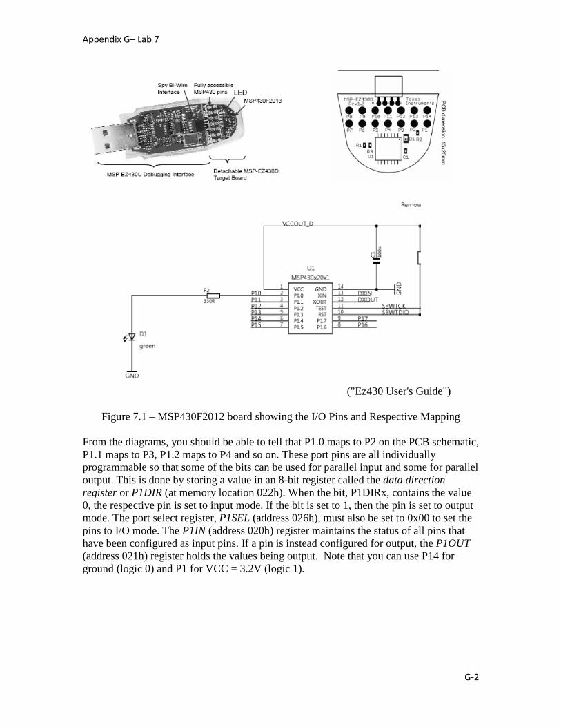
Appendix G– Lab 7
G-2
("Ez430 User's Guide")
Figure 7.1 – MSP430F2012 board showing the I/O Pins and Respective Mapping From the diagrams, you should be able to tell that P1.0 maps to P2 on the PCB schematic, P1.1 maps to P3, P1.2 maps to P4 and so on. These port pins are all individually programmable so that some of the bits can be used for parallel input and some for parallel output. This is done by storing a value in an 8-bit register called the data direction register or P1DIR (at memory location 022h). When the bit, P1DIRx, contains the value 0, the respective pin is set to input mode. If the bit is set to 1, then the pin is set to output mode. The port select register, P1SEL (address 026h), must also be set to 0x00 to set the pins to I/O mode. The P1IN (address 020h) register maintains the status of all pins that have been configured as input pins. If a pin is instead configured for output, the P1OUT (address 021h) register holds the values being output. Note that you can use P14 for ground (logic 0) and P1 for VCC = 3.2V (logic 1).

Appendix G– Lab 7
G-3
The following code shows the code you would use if you were going to use port pins P1.0 and P1.1 for output and P1.2 – P1.7 for input. Note that the assembler already has the labels for P1DIR, P1SEL, etc.
iop EQU 0x03 ; 00000011 '1' = Output '0' = Input io_mode EQU 0x0 and #io_mode, &P1SEL ; Configure P1.0-7 for parallel I/O
bis.b #iop, &P1DIR ; P1.0-1 output, P1.2-7 input The parallel I/O capabilities of the MSP430 allow it to control the outside world by connecting it to external hardware. Common external devices include:
- Push button switches - DIP switches - Light Emitting Diodes (LEDs) - Keypads - Seven segment displays
In this lab, we consider all hardware listed above except seven segment displays. Seven segment displays will be used in Lab 10 when we design a digital voltmeter. Figure 7.2 shows one way to connect DIP switches to the EZ430. These DIP switches provide 4 individual switches with 4 resistors. When a switch is in the open position, logic ‘0’ is provided to the corresponding input port pin by a pull-down resistor. When a switch is in the closed position, the corresponding input port pin is driven high and provides logic ‘1’ to the input port. The resistor limits the current flow when the switch is closed as to not damage the device. In the actual switches, the switch has a tendency to bounce. To de-bounce a switch using software, a delay must be introduced when a change is noticed to allow the switch to settle. The delay time we will use for this lab is 40ms. During this short delay, switch bouncing is effectively locked out.
Figure 7.2 Connection of DIP switches to input ports.
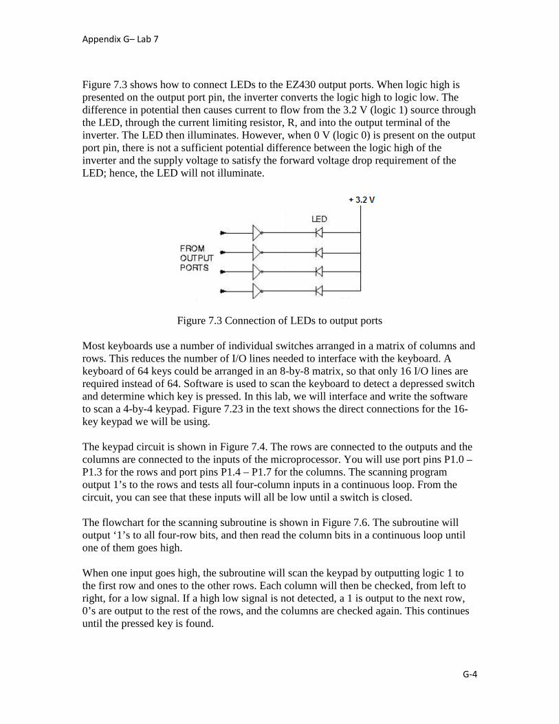
Appendix G– Lab 7
G-4
Figure 7.3 shows how to connect LEDs to the EZ430 output ports. When logic high is presented on the output port pin, the inverter converts the logic high to logic low. The difference in potential then causes current to flow from the 3.2 V (logic 1) source through the LED, through the current limiting resistor, R, and into the output terminal of the inverter. The LED then illuminates. However, when 0 V (logic 0) is present on the output port pin, there is not a sufficient potential difference between the logic high of the inverter and the supply voltage to satisfy the forward voltage drop requirement of the LED; hence, the LED will not illuminate.
Figure 7.3 Connection of LEDs to output ports Most keyboards use a number of individual switches arranged in a matrix of columns and rows. This reduces the number of I/O lines needed to interface with the keyboard. A keyboard of 64 keys could be arranged in an 8-by-8 matrix, so that only 16 I/O lines are required instead of 64. Software is used to scan the keyboard to detect a depressed switch and determine which key is pressed. In this lab, we will interface and write the software to scan a 4-by-4 keypad. Figure 7.23 in the text shows the direct connections for the 16-key keypad we will be using. The keypad circuit is shown in Figure 7.4. The rows are connected to the outputs and the columns are connected to the inputs of the microprocessor. You will use port pins P1.0 – P1.3 for the rows and port pins P1.4 – P1.7 for the columns. The scanning program output 1’s to the rows and tests all four-column inputs in a continuous loop. From the circuit, you can see that these inputs will all be low until a switch is closed. The flowchart for the scanning subroutine is shown in Figure 7.6. The subroutine will output ‘1’s to all four-row bits, and then read the column bits in a continuous loop until one of them goes high. When one input goes high, the subroutine will scan the keypad by outputting logic 1 to the first row and ones to the other rows. Each column will then be checked, from left to right, for a low signal. If a high low signal is not detected, a 1 is output to the next row, 0’s are output to the rest of the rows, and the columns are checked again. This continues until the pressed key is found.

Appendix G– Lab 7
G-5
Anytime a switch is pressed, mechanical bouncing occurs, causing the switch to open and close rapidly several times. The scanning subroutine is so fast it can scan the whole keypad before the switch gets done bouncing, missing the closed switch. A delay in the subroutine gives the switch time to stop bouncing. You can use the delay subroutine from Lab 5 to provide the delay time of 40 ms. Have your scan program call the ‘DELAY’ subroutine after a key is pressed.
Figure 7.4: Connection of DIP switches to simulate Keypad circuit. Figure 7.5 shows specifications for a Grayhill keypad, which you will use in the lab. It shows the relationship between the 16 keys, shown as 1-16 in the diagram below (0-F for our keypads), with the 8 terminals on the back, labeled E-H and J-M. Careful observation of this diagram, the key labels on our keypads (different from that shown below), and the matrix of terminal-key connections provides sufficient information to create the relationship between Grayhill’s terminal names and the port labels in Figure 7.4 above: Terminal E = Port P1.___ Terminal J = Port P1.___ Terminal F = Port P1.___ Terminal K = Port P1.___ Terminal G = Port P1.___ Terminal L = Port P1.___ Terminal H = Port P1.___ Terminal M = Port P1.___

Appendix G– Lab 7
G-6
(Fill in the blanks and include with Question 3 below)
Figure 7.5: Grayhill Series 86 Keypad Specifications

Appendix G– Lab 7
G-7
Figure 7.6: Flow chart for keypad SCAN subroutine.
Start
Output 1 to all rows
Is any
column high?
Yes
No
Read Column bits
Call DELAY subroutine
Key Number = 0x00
Row Pointer = 0x01
Output 1 to row @ Row Pointer
Read and Mask P1 Input
Is column @ Column
Pointer high?
Increment Column Pointer and Key Number
Was last column
checked?
Increment Row Pointer
Was last row
checked?
No
No
No
Yes
Yes
Yes
Save the
Key
Number
Return

Appendix G– Lab 7
G-8
7.5 Procedure: Before you come to the lab, write the individual flowcharts only (not the programs) for the following procedures and show them to the TA.
1. Configure the P1.0 – P1.3 lines as all inputs and connect them to 4 DIP switches as shown in Figure 7.2. Configure the remaining 4 P1.4 – P1.7 lines as all outputs and connect them to 4 LEDs as shown in Figure 7.3. Have the lab TA check your circuit before you turn the power ON. It would be a good idea to build this circuit before you come to the lab. Write a program to continuously read the switches connected to lines P1.0 – P1.3 and output the status to the LED’s connected to lines P1.4 – P1.7. Show the TA the working circuit.
2. Consider the situation where a F2012 is used to control a certain machine. First a
key needs to be turned on, then two switches have to be depressed at the same time (within 0.5 seconds of each other), and, lastly, a footswitch must be depressed. These steps must be performed in this order. Write a program to simulate this system. Connect the key switch to P1.0, connect the two switches to P1.1 and P1.2, and the footswitch to P1.3. The program should continuously monitor the inputs until the sequence occurs. When the sequence is done correctly, all LED’s on port P1.4 – P1.6 should light up. Show the TA when this works. A flowchart clarifying what is to be done is given in Figure 7.7.
3. Connect the Grayhill keypad to your development board as shown in Figure 7.4.
Make sure that you realize how the pins on the keypad are arranged: when the keypad is face-up, M is the leftmost pin and 3 is the rightmost pin. Write a program to scan the keypad (as described in the previous section). Include a subroutine to wait until the key is released before another key is read, as you do not want to read the key that is depressed more than once. The flowchart for this subroutine is included in Figure 7.8. Call the subroutines SCAN and NEXTKEY with the main program. Store the value of the key pressed in memory in 0x0220 and have each consecutive key pressed after that stored in the next highest location in memory.
IMPORTANT!!!! – This circuit will be used for lab 8, so do not take it apart.
7.6 Questions: 1. Is the polling method to input data very efficient? Why or why not? 2. In the keypad circuit, what will happen if your de-bounce delay is too short? What
will happen if it is too long? 3. What key is read if you depress switches 8 and B at the same time? What if you
depress 5 and 9 at the same time?

Appendix G– Lab 7
G-9
No Yes Yes Yes No No Yes No Yes No
Figure 7.7
Start
Is key
pressed?
Are key and
both
buttons
End
Are key and
button 1
pressed?
0.5 sec Delay Are key and
button 2
pressed?
Are all
inputs
active?
Light the LEDs!

Appendix G– Lab 7
G-10
Figure 7.8 7.7 Deliverables • Pre Lab Work (0.5 Point)
1. Write flowcharts for all the procedures in the lab section 7.5 and show these to your TA at the start of lab
• Lab Demonstrations (7 Points)
1. Demonstrate a working hardware implementation of all procedures in section 7.5 to your TA. This may be completed anytime between the start of Lab 7 and the first hour of Lab 8
• Lab Report (2.5 Points)
1. Cover Page 2. Flowcharts from Pre Lab work 3. Working copy of your assembly code 4. Summary of what you learned and any observations you have 5. Answers to the questions in section 7.6
Start
Call
SCAN
Display key
depressed
Call
NEXTKEY
Main program
NEXTKEY
Read
column bits
NEXTKEY subroutine
Is key still
pressed? Yes
Return
No

Appendix H – Lab 8
H-1
/ 8.1 - Objectives In Lab 7, we used the polling technique for parallel I/O. Using interrupts can improve performance of the computer and make the software easier to organize. In this lab, you will learn:
- What is an interrupt? - The difference between maskable and non-maskable interrupts. - The response of the MSP430 to a maskable interrupt. - How to write interrupt service routines (ISR) for the MSP430F2012. - How to generate delays using the MSP430 Timer_A2 Module.
8.2 - Related Material to Read
- Interrupt Vectors on the Reference Materials Page - Timer_A section in MSP430x2xx Family Users Guide - Interrupts section in MSP430x2xx Family Users Guide
8.3 - Maskable and Non-Maskable Interrupts In this lab we will deal solely with maskable interrupts which are enabled using the General Interrupt Enable (GIE) bit of the Status Register (SR). The TI-MSP430 also has non-maskable interrupts which can be individually enabled or disabled. The GIE bit can be set using the EINT (enable interrupts) command. Configuring an interrupt Before an interrupt can be used, there is some setup that must take place. One of the interrupts used in this lab is the P1 interrupt which responds to inputs on P1.0 – P1.7. The following setup must be done prior to using this interrupt.
- Set P1IE (0x25) with a 1 for each of the ports interrupts are required on (do not activate interrupts for output ports)
- Set P1IES (0x24) to 0 for a rising edge or 1 for a falling edge interrupt (determines which edge of the input an interrupt will be activated on)
Maskable Interrupts
8
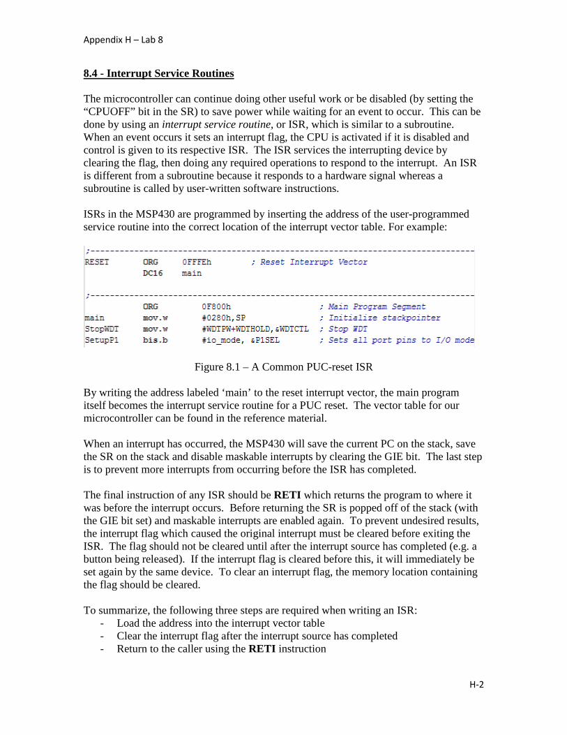
Appendix H – Lab 8
H-2
8.4 - Interrupt Service Routines The microcontroller can continue doing other useful work or be disabled (by setting the “CPUOFF” bit in the SR) to save power while waiting for an event to occur. This can be done by using an interrupt service routine, or ISR, which is similar to a subroutine. When an event occurs it sets an interrupt flag, the CPU is activated if it is disabled and control is given to its respective ISR. The ISR services the interrupting device by clearing the flag, then doing any required operations to respond to the interrupt. An ISR is different from a subroutine because it responds to a hardware signal whereas a subroutine is called by user-written software instructions. ISRs in the MSP430 are programmed by inserting the address of the user-programmed service routine into the correct location of the interrupt vector table. For example:
Figure 8.1 – A Common PUC-reset ISR By writing the address labeled ‘main’ to the reset interrupt vector, the main program itself becomes the interrupt service routine for a PUC reset. The vector table for our microcontroller can be found in the reference material. When an interrupt has occurred, the MSP430 will save the current PC on the stack, save the SR on the stack and disable maskable interrupts by clearing the GIE bit. The last step is to prevent more interrupts from occurring before the ISR has completed. The final instruction of any ISR should be RETI which returns the program to where it was before the interrupt occurs. Before returning the SR is popped off of the stack (with the GIE bit set) and maskable interrupts are enabled again. To prevent undesired results, the interrupt flag which caused the original interrupt must be cleared before exiting the ISR. The flag should not be cleared until after the interrupt source has completed (e.g. a button being released). If the interrupt flag is cleared before this, it will immediately be set again by the same device. To clear an interrupt flag, the memory location containing the flag should be cleared. To summarize, the following three steps are required when writing an ISR:
- Load the address into the interrupt vector table - Clear the interrupt flag after the interrupt source has completed - Return to the caller using the RETI instruction

Appendix H – Lab 8
H-3
8.5 - Programming the Timer module on the MSP430 In the previous labs, we used software controlled delays. By counting the number of cycles it took to execute the delay loop and multiplying by a decrementing counter, we could design rough delays for the purposes of our applications. If accurate timing is required, it is more effective to use interrupts and the provided Timer module for the MSP430, called Timer_A2. Timer_A2 is based off of its free running counter, the TAR or Timer_A Register. Depending on its mode of operation, the TAR increments or decrements every rising edge of the clock signal and holds the running count in memory location 0x0170.
Figure 8.2 – The TAR register at location 0x0170.
To activate the TAR, the Timer_A Control Register (TACTL) must be properly initialized.

Appendix H – Lab 8
H-4
Figure 8.4 – The Timer_A Control Register at location 0x0160. The Timer_A Source Select (TASSELx) bits The clock signal that the TAR register uses to count can be sourced from four different clocks according to the TASSELx bits.
TASSELx Clock Source Select 00 TACLK 01 ACLK 10 SMCLK 11 INCLK
Figure 8.3 – The Four Possible Clock Sources for TAR
We will use the Sub-Main Clock (SMCLK). The SMCLK, like the MCLK is sourced on a PUC Reset to run at 1.1 MHz. The Input Divider (IDx) Bits All clocks can be sourced directly or divided by 2, 4 and 8 using the IDx bits.
IDx Input Divider 00 1 01 2 10 4 11 8
Figure 8.4 – Input Divider bits
Assuming the TAR counter counts to 0xFFFF, with the SMCLK selected as the source and the IDx bits set to divide the clock by 1, the timer would take (1 / 1.1Mhz) * 0xFFFF or .059577 seconds. If that same clock is instead divided by eight, then the TAR register would take 8/1.1 MHz * 0xFFFF = .476618 seconds to roll over. Note how .48 seconds is about equal to .5 seconds. This will be useful for the completion of this lab. The Mode Control (MCx) Bits The four modes for the TAR are selected by setting the MCx bits: MCx Mode Description 00 Stop Timer is halted. 01 Up Timer repeatedly counts from zero to the value of TACCR0. 10 Continuous The timer repeatedly counts from zero to 0FFFFh. 11 Up/Down The timer repeatedly counts from zero up to the value of TACCR0
and back down to zero.
Figure 8.4 – The Four Timer_A Operating Modes.

Appendix H – Lab 8
H-5
For the purposes of lab 8, we will use only the “Stop” and “Continuous” operating modes. NOTE: It is strongly recommended that you stop the timer before modifying its operation or accessing the TAR register to avoid errant conditions. The TACLR Bit At any time during program execution, the user may set the Timer_A Clear (TACLR) bit to reset the TAR register. The TACLR bit also resets the IDx bits. The TAIE and TAIFG Bits Timer_A interrupts are considered maskable interrupts. Therefore, the GIE bit in the SR must be set for a flag to create an interrupt event. Additionally, the user must set the Timer_A Interrupt Enable (TAIE) bit. Setting the TAIE bit allows the TAIFG flag to be set according to the mode of operation. In continuous mode, the TAIFG bit is set when the TAR register counts from 0xFFFF to zero. Every time the TAIFG bit is set, the controller will execute its interrupt vector at location 0FFF0h. When the timer module sets the TAIFG bit, it also generates a number in the Timer_A Interrupt Vector (TAIV) register. The TAIV register is a clever method of handling multiple interrupts in one memory location for the timer module. The TAIV Register
Figure 8.5 – The Timer_A Interrupt Vector Register and Contents Table

Appendix H – Lab 8
H-6
The highest pending enabled interrupt for the timer generates a number inside the TAIV register reflecting the flag that was set. This number can then be added to the program counter to automatically enter the appropriate software routine. This means that your interrupt service routine must check the TAIV register each time it is called to see whether it was the TAIFG or TACCR1 CCIFG flag that caused the interrupt, as well as provide default behavior for other, reserved values. Figure 8.6 shows a common timer ISR. NOTE: If you notice, TACCR0 CCIFG is not in the table. TACCRx registers are capture/compare registers that will be covered in the next lab. For now, know that the TACCR0 register has its own interrupt vector so its interrupt flag will not generate any number in the TAIV. Also notice that we don’t speak of the TACCR2 CCIFG flag in the TAIV register. This is because the MSP430F2012 has only two capture/compare registers, TACCR0 and TACCR1. Other models of the MSP430 with more capability have three capture/compare registers.
Figure 8.6 – A Common Timer_A2 ISR This ISR adds the contents of the TAIV register to the program counter. Since reti is a two byte instruction and the numbers in the TAIV register increment by two depending on the flag that has been set, this ISR services both our TACCR1 CCIFG flag and our TAIFG flag while maintaining predictable results for all other instances. Any access of the TAIV register automatically resets the highest pending interrupt flag. If any interrupt requests remain, another interrupt will immediately be requested and the TAIV register will show the respective flag that was set. For code examples of how to program using the TAIV register or the Timer_A module in general, reference Timer_A2 MSP430. 8.6 - Procedure
1. Using the code and circuit from Lab 07, change the code so it uses port interrupts to run a SCAN interrupt service routine instead of polling and a SCAN subroutine. Show and explain the working code to the TA.

Appendix H – Lab 8
H-7
2. Using interrupts, write the code for a timer that executes using the following specifications:
a. P1.0 – P1.3 – display seconds on 4 LED’s; every 4 seconds, the LED’s
will increment in count. b. P1.4 and P1.5 – display minutes on 2 LED’s; after 15 second counts
(because 15 X 4 = 60 seconds), the minute LED’s should increment by one and the seconds LEDs should be reset to zero. Make P1.4 the MSB for the minute LED’s.
c. P1.6 – STOP button; pressing the STOP button should call an interrupt service routine that stops the timer.
d. P1.7 – START button; if the timer is stopped, pressing the START button should call an interrupt service routine that starts or resumes the timer.
e. P2.6 – RESET button for our timer. If at any time the RESET button is pressed, no matter what state our timer is in, it will reset our program and the user must press START to begin the timer from zero.
f. P2.7 – input from a DIP switch that control the timer divisor’s IDx bits; a high signal should divide the clock source by 4, and a low signal should divide the clock source by 8.
For the lab, initialize the timer to divide the SMCLK by 8 in Continuous Mode. The TA will then ask you to change the clock division during your demo. Note: P2.6 and P2.7 are accessed in the same way as P1.0-7 with the P2DIR, P2SEL etc. By the schematic given in Lab 7, P2.6 -7 are XIN and XOUT respectively.
Recommended Steps:
• Find out how many counts of the timer it takes to make a 1 second delay. Remember, the period is the number of counts in the TACCR0 register + 1.
• Write the ISR for the TAIV register that services a TAIFG overflow. Every 4 times the ISR is called, it should increment a counter that is output to P1.0-3.
• Anytime that P1.0-3 shows the number 15, increment the minutes counter and output to P1.4 and P1.5.
• Once this is working, look at the START and the STOP buttons. They will both be implemented using Port 1’s maskable interrupt. The ISR

Appendix H – Lab 8
H-8
will have to check the P1IFG register to see which flag has been set and react accordingly.
• Look at the RESET button. Program its respective ISR to completely reset the microcontroller and restart the timing program.
• Finally, program the DIP switch to divide the clock every time that it interrupt fires. This is a little tricky. - When the DIP switch is in its ‘0’ state, the P1.7 interrupt should be
set to the rising edge. - When the DIP switch is in its ‘1’ state, P1.7 pin interrupt should be
set to the falling edge. 8.7 - Questions 1. How are maskable and non-maskable interrupts handled differently in execution? 2. How would you program the interrupts differently if instead of using the TAIFG flag, you chose to use the TACCR0 CCIFG flag? Give specific addresses and details. When is the TACCR0 CCIFG flag set in comparison to the TAIFG flag? 3. Write the TAIV ISR to service both the TACCR1 CCIFG and TAIFG flags. Explain how the program executes the ISR and how you chose to write it. If the CCIFG is serviced, write the program to place 0xFF in R2. If the TAIFG flag is serviced, write the program to place 0x11 in R3. 8.8 - Deliverables • Pre Lab Work (0.5 Point)
1. Write flowcharts for all the procedures in the lab section 8.6 and show these to your TA at the start of lab
• Lab Demonstrations (7 Points) 1. Demonstrate a working hardware implementation of all procedures in section 8.6
to your TA. This may be completed anytime between the start of Lab 8 and the first hour of Lab 9
• Lab Report (2.5 Points) 1. Cover Page 2. Flowcharts from Pre Lab work 3. Working copy of your assembly code 4. Summary of what you learned and any observations you have 5. Answers to the questions in section 8.7 6. Marked up version of this document

Appendix I – Lab 9
I-1
9.1 – Objectives
The F2012 is equipped with a Timer Module (Timer_A2). The timer module has clock-generation circuitry to generate the internal and external clock signals used by the CPU and the on-chip peripherals, and contains two dual-function input capture or output compare channels. This lab will expand on the timer interrupt concepts from the previous lab and introduce more advanced applications of the timer module. While doing this lab, you will learn:
• How to program the input capture features of the timer system.
• How to program the output compare features of the timer system.
9.2 - The MSP430 Capture/Compare Blocks The capture/compare blocks of the MSP430 perform two main functions: Input Capture and Output Signal Generation. The input capture feature measures the characteristics of a periodic input signal such as period, duty cycle, and frequency of the signal. The output compare feature allows the generation of an output signal to user specifications, generally Pulse Width Modulated signals (square waves). Using these features, the MSP430 can also perform tasks such as pulse accumulation, where the user counts pulses (external events) on a line connected to the ports.
The MSP430 is equipped with two capture/compare registers, labeled TACCR0 and TACCR1. Each of these channels is software configurable for either input capture or output compare operation. Specific pins are used as input capture and output compare pins. For this lab, we will only use the input capture feature of the MSP430 meaning that only P1.1, P1.2, or P1.6 can be used for the Timer I/O operation.
Input Capture & Output Compare
9

Appendix I – Lab 9
I-2
9.3 - Input Capture
The capture/compare registers are initialized using their Timer_A Capture/Compare Control Register (TACCTLx) in memory locations 0x0162 (TACCR0) and 0x0164 (TACCTL1). For this lab you will be using TACCTL1. The TACCTLx register has many control bits that are important to the operation of the input capture or output compare functions. To enable capture mode, the CAP bit must be set to 1.
Figure 9.1 – The TACCTLx Register
The Capture or Compare Input Select (CCISx) Bits (13 – 12)
The CCISx bits select the TACCRx input signal. The GND and VCC pins are internal and are used for software-initiated captures. You will not use software-initiated captures in this course.
The input pins are different for the different versions of the MSP430, for the F2012 which we are using you will need CCISx bits set to 00 and your input pin will be P1.2. You will also need to set the correct pin to input mode and enable a pull-down resistor to ensure stable input levels. These settings can be found in previous labs or the MSP430 user guide.
CCISx Bits 13 – 12 Selected TACCRx input signal 00 CCIxA 01 CCIxB 10 GND 11 Vcc
Figure 9.2 – The CCISx Bits
CCIx bit I/O Pin CCI0A P1.1 CCI1A P1.2 CCI1B P1.6
Figure 9.3 – The CCISx Bits

Appendix I – Lab 9
I-3
The Capture Mode (CMx) Bits
Once you know which pin you are going to use as the I/O pin for your input capture or output compare function, you must also select which edge you want to initiate the capture using the Capture Mode (CMx) bits.
CMx bits 15 - 14 Capture Mode 00 No capture 01 Capture on rising edge 10 Capture on falling edge 11 Capture on both rising and falling edges
Figure 9.4 – The Capure Mode (CMx) Bits
Now, assume that the TACCTL1 register is set to capture mode, the input signal is tied to P1.2 and the capture mode is selected to capture a signal on the rising edge. When the capture occurs, two important events happen:
1. The timer value (the value inside the TAR register) is copied into the TACCRx register (in this case, TACCR1).
2. The CCIFG interrupt flag is set.
The CCIFG flag being set will activate an interrupt and call upon the TAIV register’s ISR so the user can process the necessary information. At any time, the input signal level may be read through the Capture Compre Input (CCI) bit in the TACCTLx register.
The Synchronize Capture Source (SCS) Bit
In many cases, the input signal can be asynchronous to the timer clock, allowing for race conditions to occur. Setting the Synchronize Capture Source (SCS) bit will synchronize the input capture with the next timer clock. For this reason setting the SCS bit is usually recommended.
Figure 9.5 – A capture event with the SCS bit set

Appendix I – Lab 9
I-4
If a second capture is performed before the value from the first capture event (stored in the TACCRx register) is read, the controller provides an overflow bit to inform the user, shown in the TACCTLx register as the Capture Overflow (COV) bit. The TACCR0 and TACCR1 registers are stored in memory locations 0x0172 and 0x0174, respectively. The COV bit must be reset by software.
Figure 9.6 – The TACCRx Register
Note that value from the first capture event is no longer available if a second capture is performed. A flow chart explaining the correct steps to handle a capture is provided below.
Figure 9.6 – A Capture Flow Chart

Appendix I – Lab 9
I-5
9.5 – Procedure For the following procedures you should remember that your counts will only be accurate at lower frequencies (less then about 4kHz) due to the limitations of your MSP430 running at 1.1MHz. For the greatest accuracy you should have Timer A running as fast as possible. 1. Write a program that uses the input capture feature of the F2012 to find the duty cycle
and the period of a square wave from the function generator. Connect the function generator signal to the correct pin and configure the capture/timer system. Save the measured characteristics as follows, Counts of high time (Duty Cycle) in R14, Counts of low time in R15. Show the working program to your TA
2. Modify the procedure from question 1 so that the period of any periodic square wave can be measured even if the period is more then the rollover time of the free running counter by counting the rollovers. Save high rollover count in R12 and low rollover count in R13. Show the working program to your TA
3. Write a program that uses the input capture feature of the Timer_A2 to count the number of rising or falling edges in the square wave from the function generator in 10 seconds. Save the count to R15 and show the working program to your TA.
9.6 – Questions
1. Give at least 2 applications for the input capture mode of the MSP430.
2. The output compare function allows you to create a pulse width modulated signal. Using similar concepts as the “Up” mode of the timer and two capture/compare registers, explain how you would output a wave of 20% duty cycle at a frequency of 1 kHz. Make the explanation general; you do not need a flow chart.
9.7 – Deliverables
• Pre Lab Work (0.5 Point) 2. Write flowcharts for all the procedures in the lab section 9.5 and show these to
your TA at the start of lab 9
• Lab Demonstrations (7 Points) 2. Demonstrate a working hardware implementation of all procedures in
section 9.5 to your TA. This may be completed anytime between the start of Lab 9 and the first hour of Lab 10
• Lab Report (2.5 Points)
1. Cover Page 2. Flowcharts from Pre Lab work 3. Working copy of your assembly code 4. Summary of what you learned and any observations you have 5. Answers to the questions in section 9.6

Appendix J – Lab 10
J-1
10.1 Objectives: The MSP430 is equipped with an analog-to-digital (ADC10) conversion system that samples an analog (continuous) signal at regular intervals and then converts each of these analog samples into its corresponding binary value using the successive approximation technique. While doing this lab, you will learn,
• How to program the MSP430 ADC10 converter system. • How to connect a 7447 BCD-to-7-segment LED display driver to a common
anode 7-segment LED display. • How to display the A/D converted signal on the 7-segment LED display.
10.2 Related material to read:
• Fundamental Concepts of the A/D Converter: Section 10.2 in the text, page 428
• Successive Approximation Method: Section 10.3 in the text, pages 429-430
• Signal Conditioning Circuits: Section 10.4 in the text, pages 430-433
• The MSP430 A/D Converter: Family User’s Guide, chapter 16 (specifically ADC10 registers)
10.3 The MSP430 Analog-to-Digital (ADC10) conversion system: The MSP430 ADC10 conversion system consists of an 8-channel, 10-bit, multiplexed input successive approximation analog-to-digital converter block. The JTAG tool provides the processor with a VCC of 3.6V, so the MSP430 cannot handle voltages higher than 3.6 volts as inputs. To emphasize, don’t provide 5V to the processor, only voltages up to 3.6V. All channels of the ADC10 are software programmable to perform either single or continuous conversion and they can be powered ON by setting the
Analog-to-Digital Converter
10

Appendix J – Lab 10
J-2
Analog-to-Digital On bit (ADC10ON, memory location 01B0h) in the ADC10 ConTroL register 0 (ADC10CTL0) to 1 (see Figure 10.1). The ADC10 requires a recovery time period of around 100 microseconds after ADC10ON bit is set to 1. ADC10CTL0: ADC10 Control Register 0: For the first control register, there are several different bits to consider when we want to set-up the converter. An explanation of the bits in ADC10 is given below.
Figure 10.1 – Analog-to-Digital Control Register 0 The SREFx bits set the reference voltages used by the ADC10. For this lab, we will use 3.6V that is provided by the JTAG tool (VCC) as the high reference voltage and VSS as the low reference voltage (see the User’s Guide for more information on these bits). So this means we want to write SREF[15:13] = 000. Next, the sample-and-hold time is set in ADC10SHTx.
ADC10SHT[12:11] # of ADC10 CLKs 00 4 01 8 10 16 11 64
Figure 10.2 – Sample and hold time for conversions
We will use 16 ADC10 clock cycles for the sample and hold time, so write ADC10SHT[12:11] = 10. The next bit, ADC10SR, selects the sampling rate of the conversion. This gives the possibility to reduce the current consumption of the converter. We don’t really care about this, so write a 0 to this bit. REFOUT and REFBURST can be ignored, so clear these bits. Moving sequentially, the MSC bit controls whether the processor does multiple sample and conversion. Writing a 0 to MSC will allow us to only start conversions with a rising edge in ADC10SC, bit 0 (to be explained later). Writing a 1 to MSC would allow for

Appendix J – Lab 10
J-3
continuous sample-and-conversion, but in this lab we prefer to only convert when we are ready, so write a 0 to MSC. Ignore REF2_5V and REFON in this lab by writing 0s to these bits. ADC10IE is the interrupt enable bit, therefore writing a 1 to this bit enables interrupts. We won’t use interrupts, so clear this bit. The ADC10IFG bit is the interrupt flag for the converter and is set when a conversion is complete. Initialize this bit to a 0 and use it later to check to see if the conversion is done. Next, ENC turns the converter on, so you should probably write a 1 to this bit. Finally, ADC10SC controls when a conversion is started. You should initialize this bit to a 0 and then write a 1 when you are ready to start a sample-and-conversion.
ADC10CTL1: ADC10 Control Register 1:
Figure 10.3 – Analog-to-Digital Control Register 1
There is another ADC10 control register, aptly named ADC10CTL1 (memory address 01B2h), and an explanation of its bits is given below. The INCHx bits select which channel(s) are to be used for input to the ADC10. If bit 15 is a zero, then the next three bits give the binary representation of the input port. For example if 011 are the last three bits, then P1.3 will be used for the input channel. The next bits in the register are SHSx, which control the signal for sample-and-hold selection. We want to use ADC10SC from the first control register as the signal to start a conversion, so SHS[11:10]=00. The data format for the converter is set in ADC10DF, writing a 0 makes the data format be binary and writing a 1 makes the data format be 2’s complement. You can use 2’s complement if you really want to, but normal binary is highly recommended. We won’t use ISSH for this lab, so write a 0 to this bit. The ADC10DIVx controls the clock divider. We won’t worry about dividing the clock, so write zeros to these bits (see the User’s Guide for more information). ADC10 is the clock source select-you can use the converter’s clock or ADC10OSC by writing ADC10SSEL[4:3]=00. The conversion sequence mode select is controlled by CONSEQx, and for this lab we want to use repeat-

Appendix J – Lab 10
J-4
single-channel conversion sequences, so CONSEQ[2:1]=10. The last bit is ADC10BUSY, a read-only bit that is set if a conversion is taking place. ADC10AE0: Analog (Input) Enable Control Register:
Figure 10.4: Analog (Input) Enable Control Register. The final register we are concerned about is the Analog (Input) Enable Control Register, or ADC10AE0 (memory address 04Ah). This byte-sized register controls which ports are used for input to the converter. So just like the I/O registers we used before, setting a 1 to one of the bits allows for input on that port. For example, setting ADC10AE[7:0]=0x20 would allow analog input only on P1.5. 10.4 Results from the ADC10: The results of the conversion are stored in ADC10MEM (memory address 01B4h). Since the ADC10 is a 10 bit converter, the results from the conversion range from 0-03FFh. In decimal, this range is 0-1023.
Result in ADC10MEM Corresponding Voltage 0x0 0.0
0x11C 1.0 0x238 2.0 0x355 3.0 0x3FF 3.6
You may want to scale this range in your program so that further calculations will have fewer rounding errors. 10.5 ADC10 Operation: There are a few things that may help with interfacing with the ADC10 when reading/writing to the control registers. It is important to write to all of the 3 set-up registers before writing to the ADC10SC bit in ADC10CTL0. This will ensure that the converter is set-up and will work correctly before starting a conversion. You can write to ADC10CTL0 but not set ADC10SC until later. It might be a good idea to check the flag (ADC10IFG) before using the data in ADC10MEM to make sure that the conversion is complete. You should clear this flag after it is set so that you can begin another conversion when ready. Also, you should use

Appendix J – Lab 10
J-5
pull-up resistors in your program, i.e. use P1REN, so that the pins are not floating and you don’t have erroneous results. 10.5 BCD-to-7 segment display: There are two types of 7-segment decoder drivers; one that produces outputs that are active high and another that produces outputs that are active low. The 7447 BCD-to-7- segment display decoder produces outputs that are active low. Hence it works with the common anode 7-segment displays, for which the anodes of all the LEDs are tied together to the supply voltage and the cathodes are connected to the decoded output of the 7447. Figure 10.12 shows the connection between the 7447 and the 7-segment display. A current limiting resistor must be used to protect each segment.
Figure 10.5: BCD to 7-segment display using 7447. When a BCD input is applied to the 7447 inputs D - A (with D being the most significant bit), the BCD number is decoded and the corresponding output is driven low. The 7447 outputs are connected to the corresponding inputs of the 7-segment displays via the current limiting resistors. A low voltage input lights up the corresponding segment on the 7-segment display. The 7-segment display package consists of two separate 7-segment displays. Hence you need to use two 7447’s to light up the necessary segments on these displays to display a 2-digit number. You can ground the pin controlling the decimal point so that it is always on for the first decimal point.

Appendix J – Lab 10
J-6
Figure 10.6: Pin-out diagram for common anode 7-segment display (from NTE,
http://nteinc.com/specs/3000to3099/pdf/nte3074_75.pdf) 10.6 Procedure: Before you come to the lab, write the individual programs and flow charts for the following procedures and show them to the TA. In this lab, you will write a flowchart and a program that will convert an analog input voltage applied to an A/D port of your choice to its digital value and will display it on the 7-segment display. Configure 6 of the remaining ports as output ports and connect them two 7447’s (one for the upper digit and one for the lower digit). Connect the outputs of the 7447’s to the 2-digit 7-segment display provided to you. For the upper digit, ground the two most significant inputs to the 7447 (C & D) so that the maximum for the upper digit is 3. Make sure you use the current limiting resistors to protect each segment of the 7-segment display. Connect pin 4 of the 7-segment display package to ground through the current limiting resistor to light up the decimal point between the two digits. Scale the result range from 000-3FF to 0000-3600 mV represented as a four digit BCD number in memory. Use the first 2 digits of this BCD number as inputs to two 7447’s through the output port and display those 2 digits on the 7-segment displays as a decimal number “X.Y”. A multiplication subroutine is provided for your use in the lab. Test your software by connecting the A/D input to GND, to VDD, and then to the analog signal input.

Appendix J – Lab 10
J-7
10.7 Questions: 1. If VRH = 4.0V and VRL = 1.0V, what digital value is returned when an analog-to-
digital system converts the following voltage using 8-bit conversion?
� 5.0 V � 0.0 V � 2.5 V � 1.5 V � 3.5 V
2. What will be the digital value when an analog-to-digital system converts the above
voltages using 10-bit conversion? 10.8 – Deliverables • Pre Lab Work (0.5 Point) 1. Write flowcharts for all the procedures in the lab section 10.6 and show these to your
TA at the start of lab • Lab Demonstrations (7 Points) 1. Demonstrate a working hardware implementation of all procedures in section 10.6 to
your TA. • Lab Report (2.5 Points) 1. Cover Page 2. Flowcharts from Pre Lab work 3. Working copy of your assembly code 4. Summary of what you learned and any observations you have 5. Answers to the questions in section 10.7 6. Marked up version of this document

Appendix K – Practical Exam 1
K-1
Instructions • The practical test consists of two objectives; drawing a flow chart, then writing a
program. • You will have a total of 90 minutes to complete all tasks. • The test is CLOSED book and CLOSED notes, however you may use all previous
labs and lab reference material. • The test is worth a total of 50 points.
The Program
• Calls a subroutine that counts the number of 1’s in the parameter passed to it • Saves the parameter in the lowest 2 bytes of RAM • Calls a DELAY subroutine to pause for 5 seconds • Calls a subroutine to complement (change 1 to 0 and 0 to 1) the lowest 2 bytes of
RAM and save in the next higher 2 bytes of RAM Objective 1 (20 Points)
• Write a flow chart for a program that completes the above tasks. Objective 2 (30 Points) Write the program and demo to your lab TA. For this objective you may approach the problem in 2 different ways. The first method is the simpler one and will have a max score of 20 points. The second method is more complicated and will have a max score of 30 points.
• Method 1 (Max 20 Points) o The parameters used may be passed “by value” through the use of a
register. • Method 2 (Max 30 Points)
o The parameters used must be stored in RAM and passed “by reference” by placing the reference on the stack for the subroutine to access.
Hints
• Look over the instruction set carefully for ideas on how to test each bit. • Separate ORG sections may help you organize your program. • Do not be afraid to leverage code you wrote in previous labs. • Do not forget to initialize the stack pointer to an appropriate location. • Call by value means the data is passed directly. • Call by reference means an address pointing to the data is passed.

Appendix L – Practical Exam 2
L-1
Procedure:
1. Write a flow chart for one procedure A OR B (20 points).
2. Write a program for one of the following procedures:
a. Implement an 8-second delay using the Timer_A system after a DIP switch connected to one of the input ports is switched on (35 points max).
i. Configure one bit of Port 1 as an output and connect one LED to it. At the start of the program, the LED should be OFF and the maskable interrupts should be enabled properly. (5 points)
ii. Configure another bit of Port 1 as an input and connect one DIP switch to it. Whenever this DIP switch is switched on, enable the Timer_A system and after every second is passed, store the second count in memory starting at 0x200 (e.g. 1 should be at 0x200, n should be at 0x200 + n). (5 points)
iii. The LED should turn ON at the end of 8 seconds and stay on until the program is reset. (5 points)
“OR”
b. Implement an 8-second delay using the Timer_A system after a DIP switch connected to one of the input ports is switched on and reset system to the starting state when the DIP switch is turned off (50 points max).
i. Complete part a (15 points)
ii. Stop the timer and reset the second count (5 points)
iii. Turn off the LED if currently on (5 points)
iv. Advance the memory pointer to the next multiple of 10 (e.g. if it currently points to 0x205, it should be moved to 0x210). (5 points)
You will need to finish as many of the tasks listed above as possible; you will get points for each of the successfully completed steps up to a maximum of 50 points if all steps work correctly. Hints:
1. You can use whichever method you prefer to monitor inputs and timers polling or interrupts.
2. Don’t forget to initialize the stack at an appropriate location. 3. You can reuse code you have written for previous labs where appropriate. 4. The switch will need to be de-bounced for proper operation

Appendix M – Lab Instructions
M-1
Lab Instructions • Labs are 1 week long, so you must demo a working version of the assignment at
the beginning of lab following the week it was due. For example if you started Lab 4 on Monday the 10th, your demo and report is due at the start of Lab on Monday the 17th.
• You are expected to work alone on each lab. Each student must turn in a lab report.
• The labs have work that must be completed in advance to the start of the lab session. This is to make sure that you can use the lab time efficiently with the TA.
Lab Reports
• Each lab report must include the following items: o Cover page with your name, class, lab #, and date. o Printed copy of any code you wrote for the lab. o Answers to all questions in the lab. o A marked up copy of the lab document. o Anything else asked for in the Lab Report section of the lab.
• Reports are due at the beginning of the following lab section. Grading
• There will be 10 labs worth 10 points each and 2 practical tests worth 50 points each for a total of 200 points.
• Labs will be graded on the following criteria. o 7 Points for demonstration of the required procedures of the lab. o 3 Points for your lab report including questions and write-up.
• Practicals will be graded on your ability to complete the assigned programming task, your ability to analyze code, and drawing flowcharts. You only have a certain amount of time to do the practicals, so make sure you know how to program under pressure.

Appendix N – MSP430 Instruction set (see References for source)
N-1