Resonant waveguide grating biosensor for living cell sensing

Graduate Theses, Dissertations, and Problem Reports
2005
Fabrication of resonant optical waveguide biosensors using Fabrication of resonant optical waveguide biosensors using
electron gun depositions electron gun depositions
Timothy Allen Cornell West Virginia University
Follow this and additional works at: https://researchrepository.wvu.edu/etd
Recommended Citation Recommended Citation Cornell, Timothy Allen, "Fabrication of resonant optical waveguide biosensors using electron gun depositions" (2005). Graduate Theses, Dissertations, and Problem Reports. 1623. https://researchrepository.wvu.edu/etd/1623
This Thesis is protected by copyright and/or related rights. It has been brought to you by the The Research Repository @ WVU with permission from the rights-holder(s). You are free to use this Thesis in any way that is permitted by the copyright and related rights legislation that applies to your use. For other uses you must obtain permission from the rights-holder(s) directly, unless additional rights are indicated by a Creative Commons license in the record and/ or on the work itself. This Thesis has been accepted for inclusion in WVU Graduate Theses, Dissertations, and Problem Reports collection by an authorized administrator of The Research Repository @ WVU. For more information, please contact [email protected].

FABRICATION OF RESONANT OPTICAL WAVEGUIDE BIOSENSORS USING ELECTRON GUN DEPOSITIONS
by
Timothy Allen Cornell B.S.E.E, West Virginia University
Thesis submitted to the College of Engineering and Mineral Resources at
WEST VIRGINIA UNIVERSITY
in partial fulfillment of the requirements for the degree of
Master of Science in
Electrical Engineering
Committee members:
Dr. Dimitris Korakakis, Committee Chairperson Dr. Lawrence A. Hornak
Dr. Mark Jerabek
Lane Department of Computer Science and Electrical Engineering
Morgantown, West Virginia 2005
Keywords: biosensors, electron beam deposition, FT-IR, ellipsometry

Abstract
Electron Beam Thin Film Depositions
Tim Cornell
Biosensors are used to connect the chemical and physical worlds through the use
of a transducer, allowing for quick detection of numerous biological agents. A new
biosensor being developed, the resonant optical waveguide biosensor, uses power transfer
between two optical waveguides to detect the presence of an antigen. The condition for
power transfer is extremely sensitive to changes in index of refraction and allows the
biosensor to have a high sensitivity to the antigen presence. Given the high sensitivity of
the device, a high degree of accuracy in index of refraction and thickness is required from
the fabrication process.
Fabrication of the biosensor transducer was performed from Electron Beam
Physical Vapor Depositions. This thesis outlines the development of the protocol for the
fabrication process and discusses the improvements made to the deposited films as new
capabilities were added to the evaporation chamber such as substrate heat and Ion Beam
Assisted Deposition (IBAD). Also discussed is the numerous characterization techniques
used to optimize the fabrication protocol.

Table of Contents Chapter One – Introduction 1.1) Biosensors 1 1.2) Thin Film Fabrication 2 1.2.1) Physical Vapor Depositions 3 1.2.2) Characterization Techniques 5 Chapter Two – Theory 2.1) Biosensors Operation 7 2.2) Vacuum Components 10 2.3) Vapor Depositions 14 2.4) Electron-Gun Physical Vapor Depositions 16 2.5) Ion Beam Assisted Depositions 17 2.6) Properties of Gases and Vapors 21 2.6.1) Kinetic Theory of Gases and Vapors 22 2.6.2) Transport Theory 26 2.7) Surfaces 27 2.8) Contamination and Substrate Cleaning 29 2.9) Characterization 31 2.9.1) Characterization using Fourier Transform
Infrared Spectroscopy 31 2.9.2) Characterization using Ellipsometry 38 Chapter Three – Experimental 3.1) Silicon Dioxide from Electron-Beam Depositions 45 3.1.1) Silicon Dioxide Depositions with Substrate Heat 53 3.1.2) Silicon Dioxide Depositions with Ion Beam Assist 56 3.1.3) Silicon Dioxide Reactive Depositions 60 3.2) Sweep Pattern Selection 61 3.3) Aluminum Oxide from Electron-Beam Depositions 65 3.3.1) Aluminum Oxide Depositions with Substrate Heat 70 3.3.2) Aluminum Oxide Depositions with Ion Beam Assist 73 3.3.3) Aluminum Oxide Moisture Stability 77 3.4) Structure Growth 80 3.4.1) Thickness Control Measurements 81 3.4.2) Ellipsometry, Prism Coupler, and Simulation Results 85

3.4.3) Surface Roughness 87 Chapter Four – Conclusions 4.1) Improvements 90 4.2) Improved Thickness Control 90 4.3) Decreased Surface Roughness 91 4.4) Reactive Depositions of Aluminum Oxide 91 4.5) Ion Scrubbing, In-situ Surface Cleaning 91

1
Chapter One - Introduction
• Section 1.1 Biosensors
The biosensor is a device that connects the biological world to the physical world [1].
Its three main components being the biological sensitive element (enzyme, antibody,
etc.), the detector element which responds to changes in the biological element in some
physical way (optical, electrical, magnetic, etc.), and the transducer in between which
links the two. While many biological agents can be easily detected through more
traditional means involving reagents, these processes are often time consuming and only
possible in the laboratory environment. By including the receptor and the transducer into
the biosensor device an analysis is completed quickly and can be performed in a variety
of environments.
The traditional market for biosensors has been the detection of glucose for diabetes
patients but is now finding a market in other fields [2]. They are currently in use for or
being considered for the detection of a wide range of biological agents such as toxins,
pathogens, and nutrients. The first commercial biosensor reached the market in 1975.
Referred to as an amperometric biosensor it was used as a glucose analyzer by placing a
silver anode and platinum cathode into a KCl and glucose solution. The reduction of
oxygen from glucose oxidase at the cathode resulted in a current flow through the
solution which was proportional to glucose concentrations. The same year biosensor
research moved into the field of thermal biosensors which were used to measure the
amount of heat generated by an exothermic reaction between an enzyme and a reactant.
Also in 1975 biosensor research entered into the optical world with a fiber optic
biosensor capable of detecting carbon dioxide or oxygen.
The resonant optical waveguide biosensor was first proposed by Don Lloyd and
Harry Loats of Loats Associates Incorporated [3, 4]. This biosensor operates by sensing
small changes in the index of refraction of the analyte located above two optical

2
waveguides separated by a buffer layer of lower refractive index. An exponentially
decaying electromagnetic wave, called an evanescent wave, which extends beyond the
boundary of one waveguide and into the second waveguide allows for total power
transfer back and forth between the two. This condition, known as coupled mode theory,
is also very sensitive to the interaction of the evanescent wave with the layer above it, in
this case the biolayer. The biosensor can be engineered so that this condition, known as
resonance, only occurs when a specific biological agent has attached itself to the
bioreceptor [3].
• Section 1.2 Thin Film Fabrication
A thin film is deposited onto a substrate when the properties required for a certain
application are not obtainable from the thin film material in bulk.
Property Application
Optical waveguides, antireflective
coatings
Electrical insulating barriers,
semiconductors
Mechanical hardness, adhesion
Chemical protective barriers against
oxidation of diffusion
Magnetic magnetic disks
Thermal heat sinks Table 1.2.1 [5]
In addition, alternating layers of different thin film materials can often produce structures
with completely new physical properties. Because of this, thin film processes have found
their way into almost all manufacturing processes, from the automotive industry to
cutting edge electrical and optical waveguide circuitry.

3
In a thin film process, source material, which may be in a solid, liquid, vapor, or
gas phase, is transported to the substrate where it attaches to the surface. For transport to
take place from condensed source materials vaporization by heat or an energetic stream
of electron, ions, or photons must occur. The properties of the transport phase can
significantly affect the final properties of the thin film. If transport of the source material
occurs through a high vacuum the material will arrive line-of-sight. This prevents oddly
shaped substrate or side walls from photolithography processes from being covered and is
often associated with physical vapor depositions. The final uniformity of the deposited
film is dependent upon the geometry of the substrate holder and the chamber itself.
Source material that is not transporting through a high vacuum (fluid-flow regime) will
undergo many collisions with surrounding molecules before reaching the substrate. This
allows for depositions on substrate with a variety of geometries. Thickness uniformity on
the substrate is determined by gas flow patterns and diffusion.
Substrate conditions can result in serious modification of the thin film properties.
Surface conditions (roughness, contamination, chemically active sites, crystallographic
plane, etc.), reactivity of the transporting material, and additional energy input are the
three principal factors of concern. Reactivity is dependent on the substrate and the
material being deposited but is related to the “sticking coefficient” or the probability of a
molecule that arrives at the substrate sticking to the surface and becoming part of the
depositing film.
• Section 1.2.1 Physical Vapor Depositions
In Physical Vapor Depositions (PVD) the molecule sticks to the surface in a
weakly bonded state known as physisorption. Numerous methods have been developed
for performing these types of depositions.
Physical sputtering involves the acceleration of an ion towards a source target
where several atomic collisions take place and one or more target atoms are ejected

4
backwards from the target. A glow-discharge plasma is generated when a free electron is
placed inside a gas and a electric field. The electron is accelerated through the gas due to
the field and undergoes many collisions with gas molecules generating ions, and more
electrons due to secondary electron emission. The resulting positive ions are accelerated
away from the ion gun and towards the target where the targets atoms are sputtered.
Resistively heated thermal evaporators involve placing the source material into a
small boat or crucible and passing a high current (several hundred amps) though it.
Crucibles or boats are made of material with low electrical resistances and high melting
temperatures such as tantalum, tungsten, or molybdenum and are good for thin film
depositions when the material vaporizes at temperature below 1500˚C. Over time the
molten material can weakly bond to the container or to an oxide layer formed on the
container and the thermal expansions occurring during heat up and cool down may result
in cracking of the container. As the container age’s microcracks form and local hotspots
occur resulting in vaporization of the container itself and contamination of the depositing
film. Because of these limitations radiations shields are often used to prevent radiant heat
loss and allow for depositions are lower power.
Radio frequency (rf) heated sources involve coupling rf energy into the source
material or into a container holding the source material. This method has many of the
same disadvantages as the resistively heat thermal evaporator when used with a
conductive container but has been found to suffer less contamination when the energy is
coupled directly into the source material.
Laser Ablation Deposition (LAD) involves using a high powered laser, usually a
YAG or ArF, to deposit material in pulses. Using LAD high quality superconductors
have been formed at low substrate temperatures. Depositions of patterns have also been
achieved by shining the laser through a transparent substrate and vaporizing a film
located near the substrates backside. LAD often produces vapor that is highly directions
which makes it difficult to deposit on large areas.

5
Electron beams are often required for the depositions of thin films from materials
which vaporize above 1500˚C. In electron beam deposition a filament is held between
10-50kV below a copper hearth which contains the source material. A small potential is
applied across the filament until enough current is passing through it so that electrons are
thermionically emitted from it. The electrons are accelerated through the potential
difference and steered towards the source material by magnetic deflection. The high
energy electron bombardment can result in secondary electron emission from the source
material leaving it with a positive charge after the electrons are quickly drawn towards
ground. In dielectric substrates charge can build due to these positive ions and begin to
repel ionized source material from the substrates surface. Also the high energy electrons
can generate x-rays when they strike the source material damaging the depositing films
and substrates.
Chemical Vapor Depositions (CVD) occurring when the reaction of two products
results in a deposited film and some byproduct such as the reaction of silane (SH4) with
oxygen to form silicon dioxide. An activation energy is required for the reactions to take
place and can be added to the process in many different ways. Thermal CVD
accomplishes this by raising the substrate temperatures to the required levels. A more
common technique known as Plasma Enhanced Chemical Vapor Depositions (PECVD)
overcomes the required activation energy through the use of charged particles from a
glow-discharge plasma which allows for depositions at relatively low substrate
temperatures while simultaneously allowing for ion bombardment for film structure
improvements.
• Section 1.2.2 Characterization Techniques
The ability to accurately determine the chemical and physical properties of thin films
is required for the optimization of the growth process. Thickness, refractive index, film
intermix, surface roughness, stoichiometry, and material strain are common thin film
characteristics of interest.

6
IR spectroscopy uses the amount and location of absorption in the infrared spectrum
to determine chemical bonding and molecular makeup in the films. Traditional methods
involving the use of a monochromator and a slit to separate light from a broadband
source are sometimes used but have mostly been replaced by interferometers in Fourier
Transform Infrared Spectroscopy (FT-IR) which is capable of quicker analysis and higher
spectral resolution.
The IR spectra of many thousands of different compounds are available in computer
databases and IR data collection software can often rapidly identify compounds under
investigation. If unable to make a positive match, the chemical bonds present can easily
be extracted from a spectrum giving a good indication of the material present. This
technique is particularly useful in vacuum systems where contamination control is
critical. The IR spectrum of the thin film itself can be referenced out of the collected
spectrum leaving only a spectrum of any contaminants that reside in the film.
Atomic Force Microscopy (AFM) is based on the forces experienced by a tip as it
comes within a few angstroms of a surface. A tip of around 50nm in radius is attracted
by the van der Waals forces it experiences when it comes near or in contact with the film
surface. Although the highest resolution images come from AFM when the tip comes
into contact with the surface itself, it is sometimes necessary to restrict the amount of
force on the surface for fear of damage. In tapping mode the AFM tip is vibrated above
the surface of the sample, gently striking the surface each cycle but exerting less force on
the surface than in contact mode. In non-contact mode the tip is again vibrated but is not
allowed to come into contact with the film surface. While scanning the tip above the
surface van der Waals forces change the amplitude of oscillation of the AFM tip.
Scanning Electron Microscopy (SEM) can be used to view a sample in an optical like
manner but with the ability to resolve features that are much smaller than the wavelength
of visible light. High energy electrons bombard the surface of the sample and secondary

7
electrons are emitted. Secondary electron intensity and angle of emission are used to
construct a visual image of the sample’s surface morphology.
Ellipsometry is a powerful tool that allows for the determination thin film thickness,
refractive index, and even microstructure. The focus of ellipsometry is to study the shape
of elliptically polarized light that reflects off of a thin film or stack of thin films; or more
specifically the ratio of amplitudes and phase difference between the parallel and
perpendicular polarizations of the reflected light. By creating a general first estimate of
the Fresnel reflection coefficients based on a model provided by the operator the
ellipsometer can then slightly modify the operator’s parameters to fit the model to the
actual Fresnel reflection coefficients it has derived from the ratio and phase difference for
the two polarizations. A more recent advance in ellipsometry techniques is the
spectroscopic ellipsometer which collects data at many different wavelengths from the
UV to the IR.
Chapter Two - Theory
• Section 2.1 Biosensor Operation
The resonant optical waveguide biosensor works by using two dielectric slab
waveguides that are separated by a material of lower index all of which are deposited
onto a substrate also of lower index.
Figure 2.1.1 [6]

8
For the resonant optical waveguide to work, light must propagate through the
waveguide by total internal reflection. This occurs at all angles above what is known as
the critical angle, which is given by
1
2sinnn
c =θ Equation 2.1.1
where n1 = index of refraction of material light is traveling in n2 = index of refraction of material just beyond the interface
If the material on either side of the slab waveguide is not of the same index then their will
be a different critical angle for each reflection and the overall critical angle will be the
greater of the two.
Although an electromagnetic wave will be totally reflected inside a waveguide
when its incident angle is above the critical angle for both interfaces, due to lights wave
nature the wave may not be sustainable. Electromagnetic waves can only propagate
through a medium at certain angles known as “modes.” At other angles the wave reflects
off of one interface and overlaps with the incoming wave and destructively interferes.
For the resonant cavity of a laser, the cavity length itself must be an integer multiple of
one half the wavelength of the light inside the cavity
2λmL = Equation 2.1.2
For a standing wave to occur and the electromagnetic wave not to destructively interfere
with itself. Optical waveguides are similar in that the phase shift of the wave in one
complete round trip must be equal to an integer multiple of 2π.
πφ 2m=∆ Equation 2.1.3

9
Figure 2.1.1
Figure 2.1.2 [7]
Even though at angles above the critical angle light is completely reflected from
an interface, the wave traveling through a medium does not cease to exist beyond the
interface. The exponentially decaying field extending beyond the interface is known as
an evanescent wave and fades as ze α− Equation 2.1.4
where
22
2210 sin nnk i −= θα Equation 2.1.5

10
The evanescent wave and Coupled Mode Theory are essential to the understanding of the
resonant waveguide. If two dielectric waveguides are close enough together that the
evanescent wave of one extends into the other, then Coupled Mode Theory finds that the
electromagnetic wave can be transferred into the second waveguide after traveling some
distance inside the first. The wave will then in turn travel some distance in the second
waveguide before transferring back into the first waveguide. This resonant condition is
very sensitive to the index of refraction of the medium just above the top waveguide
which allows the sensor the ability to detect such small quantities of biological agents.
This puts strict tolerances onto the biosensor manufacturing itself, because small changes
in thicknesses or refractive indices could prevent the device from entering into its
resonant condition when the agents to be detected are present.
• Section 2.2 Vacuum Components
Vacuum systems contain numerous components. For the greater than one percent
in thickness accuracy that the biosensor requires it is imperative that all these components
operate in a predictable and reproducible manner.
All vacuum systems consist of at least one type of pump. A mechanical pump,
such as an oil sealed pump, dry pump, or a diaphragm pump, is often used to pump large
amounts of gas out of a system. It is usually the first stage pump and is used to bring the
chamber from atmosphere down to a specific pressure where a second pump will begin to
operate. Sometimes referred to as positive displacement pumps, first stage pumps
operate by capturing, compressing, and then expelling the gas collected [7].
Sorption pumps capture and hold gas molecules and are mostly used in high
vacuum applications. A cryopump is type of sorption pump that uses progressively
colder temperatures in the interior of the pump to trap gases, usually reaching
temperatures down to 10 – 20 Kelvin. If a gas solidifies at or above those temperatures it
11
will form a solid and become trapped inside the pump. This is the case of many gases
such as O2, N2, CO2. For gases that do not solidify above the cryopumps operating
temperatures it is still possible to trap the vapors by cryosorption. Even though the
vapors may not condense, they can be cooled to such a degree that the molecules stick for
a long periods of time when they reach the walls of the chamber. This process is
exploited in the cryopump by a porous charcoal cylinder which provides greater surface
area for the vapor molecules to stick to. Gases such as H2, Ar, Ne, and He are trapped in
this manner.
Deposition of thin films with a high degree of accuracy would not be possible
without some type of in-situ thickness monitoring. Optical measurements are extremely
accurate ways to accomplish this but typically require a beam of light to enter into the
chamber, reflect off the depositing film, and then exit the chamber to a detector. Optical
measurements are also typically not accurate for films that are orders of magnitude in
thickness above or below the wavelength of the light used. A more common way of in-
situ thickness monitoring is by monitoring the mass deposited on a small surface inside
the chamber, often a small crystalline quartz wafer. Electrical contacts are made to the
crystal and the deposition controller monitors the resonant frequency at which the quartz
crystal is oscillating. As mass accumulates on the surface of the crystal the resonant
frequency of the crystal will change, this can be modeled as a mass-spring oscillator.
mk
Tv
vr π2
11== Equation 2.2.1
vr = resonant frequency, Hz Tv = vibration period k = mass spring constant, N/m(kg/s2) m = mass, kg
and
+=
q
fqv m
mmT
211 Equation 2.2.2

12
mq = initial mass of crystal mf = final mass of crystal
This measurement requires a change from a mass measurement to a thickness. Therefore
it is required that the density, g/cm2, be known for the material being deposited. This can
be a source of inaccuracy in the measurement if the density of the material is changing
between depositions or even during deposition due to growth conditions. An account
must also be made for the fact that it is not just the mass that is changing during
deposition, the spring constant of the system overall is changing. This is observed as the
acoustic impedance of the crystal/mass system and is known as the z-factor which is
different from material to material. It must also be noted the quartz crystal will almost
certainly be fixed to one position in the chamber and some correction factor must be
determined to relate the thickness deposited at the stationary crystal to that of the rotating
substrates.
The power of the crystal mass monitoring system is that it is a relative
measurement, which in general is more accurate than absolute measurements. Common
sources of inaccuracy in these measurements come from strain, which forms in the films,
and from the temperature dependence of the quartz crystals. If strain is found in the films
then quartz crystals will interpret this as a greater mass than is actually found on the
crystal surface. A characteristic sign of this is a sudden negative shift in thickness when
the stain is released in the films, often from cracking. Even greater sudden loss of
thickness can be seen if the strain causes some of the film to crack and flake off of the
crystal. For systems capable of monitoring from two different crystals located in the
chamber at the same time it is possible to place crystals of different orientations inside
the chamber. Growth on crystals of different orientation will often induce different
amounts of strain in the films that will be detected as a difference in thickness.
Radiation due to multiple sources from inside the chamber can also affect the
stability and accuracy of the thickness measurements. The greater the stability of the
chamber temperature throughout the deposition process the greater the accuracy of the
measurement overall can be considered. Water cooling is often added to crystal monitor

13
heads to alleviate the sudden surge in radiation seen by the quartz crystal when the
shutter is first open, often seen as a sudden drop into negative thicknesses. The crystal
must absorb this heat and stabilize before accurate deposition rate can be achieved.
While crystal monitors are used mostly during the deposition process, a wealth of
information can be obtained from them before and after the process itself. A sensitive
measurement of sputtering rate can be determined from the crystals if an ion source is
being used inside the chamber as long as care is taken to ensure that the monitor and
electrical feedthroughs are correctly grounded. When a chamber is vented to atmosphere
water may be absorbed into the films or oxidation may occur. In this case the crystal
monitor can serve as a sensitive microbalance (±0.01 µg) for which porosity or water
absorption can be determined.
Pressure gauges inside the chambers are primarily used to determine when one
process can end and another can begin, (close roughing pump and open cryopump, begin
deposition, etc.) but can also be used to determine pressure gradients inside the system if
multiple gauges are present. Two simple pressure gauges that are often only used at low
vacuum pressures are the thermocouple and Pirani gauge that are based on the removal of
thermal energy by the gas still remaining inside the chamber. A voltage is placed across
a simple coil and a thermocouple is attached. When negligible background gas is present
inside the chamber a steady state is reached where energy lost from the heated coil is only
from radiation. When enough background gases are present though they will conduct
some heat away from the coil, which based on heat-transfer and fluid-flow models, can
give the background pressures inside the chamber.
The ion gauge, which is often operated at pressures below 10-2 torr, uses an
electron emitting filament, kept at positive potential, and a wire grid, kept at a higher
positive potential, to determine background pressures. Electrons leave the filament due
to field emission and are accelerated towards the wire grid due to the electric fields
generated. Ionization of gas in the ion gauge creates an ionization current through the
wire grid which is related to the emission current, ionization cross section, and gas

14
concentration. The major drawback of the ion gauge is that different gases have different
ionization cross sections and each ion gauge must be calibrated for the gas it will be used
in. A ion gauge calibrated for air will not report a correct pressure reading in an oxygen
rich atmosphere.
Shutters inside a vacuum chamber are placed to perform melt-ins of source
material without depositing onto the substrates. A shutter is usually just a small flat disk
or a cone shape if source material is diffusing around the shutter and making its way to
the substrate.
Substrate heaters can be added to a vacuum chamber for chamber bake out and for
substrate heating. Laser and electron emission can be used for heating but the most
common technique is the use of radiation from a quartz lamp. Thermocouples are
installed inside the chamber allowing for in-situ monitoring of the chamber temperature
but are often only estimates as it is difficult to relate the temperature of the stationary
thermocouple to the rotating substrates. Some materials, such as SiO2 are also very
transparent in the IR which leads to further inaccuracies. Temperature sensitive tapes can
be applied to the back of the substrates and are useful for determining the correlation
between thermocouple temperature and substrate temperature.
• Section 2.3 Vapor Depositions
Vapor depositions can be spilt into two categories, Chemical Vapor Depositions
(CVD) and Physical Vapor Depositions (PVD) [8]. In Chemical Vapor Deposition’s
gases are used as the source material rather than solid source materials. Condensation of
the gases, and formation of the thin film, generally only occurs on surfaces that are above
room temperature. Although a monolayer or two of gas may condense onto the chamber
walls, condensation is generally restricted to the substrate which is often held at
temperatures well above room temperature. The use of gases rather that solids as the

15
source material and the ability to work at a variety or pressures allows operations in the
two different process regimes, high-vacuum and fluid flow, where line of sight deposition
is not required. The ability to operate in fluid-flow regime allows the gases to diffuse
around oddly shaped geometries and condense on a variety of substrates, known as
conformal coating, without the need to change sides of the substrate during deposition.
The classic chemical reactions that occur in CVD can be broken into five
categories: pyrolysis, oxidation, hydrolysis, reduction, and displacement. In pyrolysis
heat causes the deposition of one chemical compound into another such as in the reaction
SiH4(g) → Si(c) +2H2(g). Oxidation is the addition of oxygen or the removal of
hydrogen from a substance, such as in the reaction
SiH4(g) + 2O2(g) → SiO2(c) + H2O(g). Hydrolysis is the process where a molecule is
spilt into two by the addition of a water molecule, such as in the reaction
2AlCl3(g) + 3H2O → Al2O3(c) + 6HCl(g). Reduction, the opposite of the oxidation
reaction, is the removal of an oxygen or the addition of a hydrogen, such as in the
reaction WF6(g) + 3H2(g) → W(c) + 6HF(g). Finally, displacement is the reaction where
one element replaces another in a compound or when the cations and anions of two
compounds trade places, such as in the reaction
Ga(CH3)3(g) + AsH3(g) → GaAs(c) + 3CH4(g). The main drawback of CVD can be seen
in the reactions above; all of these reactions either use or produce as a byproduct a
dangerous gas. A large segment of a CVD system will often be dedicated to safety,
insuring that no leaks or valve failures occur.
The source gases used in CVD are generally not found in nature but are fabricated
by reacting a desired element with a terminating radical, i.e. an atom or functional group
with only one dangling bond. This fabrication often occurs at facilities other than the one
where the CVD deposition will occur and the gas must be delivered to the facility. This
fabrication and delivery increases the overall cost of CVD depositions as compared to
PVD and provides a major entry route for contaminants.

16
• Section 2.4 Electron Gun Physical Vapor Depositions
The basis of the electron beam gun is the electron emitting filament [9]. Electrons
are thermoionicly emitted from a heated filament and accelerated through a 10kV voltage
drop away from the filament. The electrons are then curled through an 180˚ path rotation
by a magnetic field which leads them towards the source material pockets. The
combined force of electric and magnetic fields on the electron is given by
BvEFFF ×+=+= eeBE qq Equation 2.4.1
where v is the velocity of the electron given by
e
e
mVq
v2
= Equation 2.4.2
me is the mass of the electron, 9.11x10⁻³¹ kg and qe the charge of the electron -1.6x10⁻¹⁹
C. The first force term in the equation, qeE, is the force that accelerates the electrons
away from the filament towards the grounded source pockets, and is equal to the charge
of the electron multiplied by the voltage drop between the gun and the pockets. The
second is the force acquired by the electrons due to the large magnet inside the electron
gun which produces a magnetic field perpendicular to the direction of the traveling
electrons. The electrons are then curled due to the centrifugal force with a radius given
by the cyclotron radius of an electron orbiting in a magnetic field which can be found by
Be
ec q
vmr = Equation 2.4.3
where ν is the component of the electron velocity that is perpendicular to the magnetic
field B. Using equation 2.4.2 and an accelerating voltage of 10kV the velocity of an
electron leaving the filament can be found to be 5.9x10⁷ m/s. In a field of 10-2
webers/cm2 (100 gauss) the radius of the electron path is found from equation 2.4.3 to be
3.4 cm, a typical source to filament distance for an electron gun.
For all materials, at some point during the deposition, it is required to move the
electron beam around the surface of the evaporant material. This is particularly true for

17
materials such as SiO2 and Al2O3 because of their low thermal conductivity. If the beam
is allowed to rest in one position it would quickly evaporate all the material in one
location of the pocket and begin striking the bottom of the pocket. Scanning the beam is
accomplished by two steering solenoid coils. The first coil, the longitudinal coil,
produces a magnetic field in the same direction as the permanent magnet. This coil adds
to the magnetic field and decreases the cyclotron radius which allows the electrons to be
curled tighter and pushed towards the front of the pocket. The second coil, the latitudinal
coil, produces a magnetic field that runs parallel to the plane of the copper hearth. This
coil can produce a field pointing in either direction which creates a force pushing the
electrons either to the left or to the right of the center of the evaporation source pockets.
In addition to the permanent magnet and the steering coils, four beam forming
magnets are inside the electron gun. These magnets determine the size, shape, and
intensity of the spot on the source pocket.
• Section 2.5 Ion Assisted Depositions
Ion Plating, or as it is more commonly referred to, Ion Assisted Deposition is the
process of continually bombarding the depositing films with energetic particles, either
ions or atoms. Advantages to this process are numerous, including in-situ substrate
cleaning, increased adhesion, and modification of film properties such as index of
refraction, film stress, and material stoichiometry [11, 13]. Although the process that
creates the thin films in a vacuum deposition can also be responsible for the creation of
the energetic particles, more commonly ion generation is a separate process referred to as
Ion Beam Assisted Deposition (IBAD).
For most ion sources the ionization process begins by the inducing highly
energetic electrons into the gas to be ionized. For “hot cathode” sources the generation of
electrons comes from the thermoelectron emitter, essentially the same as the electron-gun

18
in an electron-beam evaporator. Current is passed through a filament until electrons
traveling inside the filament gain enough thermal energy to break away from filament.
This process is very popular in ion sources but has a major drawback that the ionization
energies may drift as the ion source heats up. In contrast cold cathode ion sources
operate without the need for a hot filament.
In cold cathode ion sources, gas enters into a compact chamber inside the ion
source head where it becomes ionized due to a large electric field. The large applied
voltage and small size of the ion source head force electrons to leave the cathode and
travel through the ionized gas. The presence of a strong magnetic field inside the source
head, due to the placement of several permanent magnets, prevents the electrons from
traveling directly from the cathode to the anode. Due to the Hall Effect the electrons are
instead steered in a circular fashion inside the source head. This increases the ionization
by increasing collisions between electrons and gas molecules.
Ions leaving the ion source head are drawn towards the chambers walls which are
held at ground. If non-conducting materials are being deposited inside the chamber
electric charge will form on the inside of the chamber walls. The continuing
bombardment of ions onto the substrate will result in charge build up and cause columbic
repulsion of material from the substrate surface. To counteract this effect a hot filament
is placed outside the ion source head which injects low energy electrons into the ion
stream. These electrons do not neutralize the ions inside the beam but simply neutralize
the ion stream as a whole leaving it a plasma.
When a plasma comes close to a substrate, a negative potential will form on the
substrate. This potential, called the sheath potential, will form because of the more rapid
loss of electrons from the plasma to the surface than the loss of ions. This potential will
increase the force with which the ions strike the substrate surface and cause desorption of
unwanted molecules from the surface, referred to as “ion scrubbing”. If the energies of
the impinging ions are great enough then they will be capable of physically sputtering the
surface of the substrate. To increase momentum transfer between collisions and prevent

19
any sorts of reactive processes this technique is usually only performed using large, inert
atoms such as argon.
The improvements from IBAD result from the ability of the ions to transfer a
portion of their momentum to the atoms or molecules on the surface of the depositing
film. This energy transferred is referred to as the recoil energy as is given by the
equation [12]
iti
tim E
mmmmT 2)(
4+
= Equation 2.5.1
Tm = energy transferred mi=impinging particle mass mt=target particle mass Ei=initial energy of impinging particle
For an oxygen atom with a mass of 16u and an energy of 75 eV which strikes an
Al2O3 molecule with a mass of 101.9u the energy transferred is 35.19 eV. In contrast, if
the impinging atom were an argon atom (mass equal to 40u) the energy transferred would
have been 60.73 eV. While having the ion mass and the mass of the particles being
deposited would produce the most efficient use of the ion source, one particle being
within 50% mass of the other produces close to a 90% energy transfer which is
acceptable in most instances. For this reason argon is one of the most common gases
used ion sources, as it is the most common of the heavy inert gases. For processes that
require reactive deposition, the use of the ion gas to form some other compound, a certain
gas will be required and the reactive gas will be mixed with argon to increase the overall
energy transfer between the ions and the surface particles.
Knowing the energy of the bombarding particles can give a great deal of insight
into the deposition process. To that end, some ion sources will use a separate grid to
steer ions of unwanted energies away from ion stream towards ground. Only ions of a
certain energy or range of energies will be allowed to escape the ion source head. This
design has the drawback of producing low ion current densities. Therefore most ion
sources are of the “gridless” design where ions of a range of energies are produced.
Unfortunately the spectrum of energies produced is not easily gathered and requires
20
characterization to be performed on the system that the ion source is installed on. In
addition, the energies of the ions that leave the ion source are really of no interest to the
process engineer. The value of most concern is the energy with which the ion has when it
reaches the sample surface. If the ion suffers any collisions during transport with
background gases it will lose some energy. Energy loss will also occur if the ion
becomes exposed to an electric field. This is very important with the deposition of
dielectrics as the films often have some charge to them due to the electron beam
deposition or from the ion stream itself.
When the ion arrives at the sample surface and collides with an absorbed particle
that particle will gain a portion of the impinging particles’ energy. The absorbed particle
may now be freed from any intermolecular bonding that was occurring before and move
around on the substrate. It may also desorb from the substrate and reabsorb at a different
location on the substrate or it may leave the substrate completely. The ion source has
given the atoms on the film’s surface enough energy so that they may move around and
fall into microscopic features such as pits or smooth out any bumps that have formed on
the surface.
A high quality thin film should have a density close to that of the bulk material,
low stress, and none of the gas used for the ion stream incorporated into the film. While
adding IBAD to a deposition process has many benefits it is possible to increase the
energy of the ions to a point where they begin to harm the overall deposition process.
Bombardment of a thin film with overly energetic ions can increase the diffusion of the
new material into the underlying film or substrate, reducing the abruptness of the
interface. Bombarding ions will also heat the top few monolayers of the material
increasing interdiffusion between an interface. While that may be advantageous in select
instances, for optical coating where sharp transitions in the films are needed this harms
the functionality of the device.
In addition to increasing the density of a film ion bombardment can also increase
the compressive stress inside a film. If this stress increases beyond a critical point the

21
films adhesion will decrease; cracks may form or the film may separate itself all together
from other films or the substrate. Cracks and other problems can also occur if the ions
become implanted inside the films. The gas used to form the ions will remain inside the
films and increase the porosity of the films. The implanted gas may make its way outside
of the film at a later time through the formation of a crack. This is particularly noticeable
if the substrate temperature is kept to low; higher substrate temperatures will often allow
any gas that sticks inside a pit in the depositing film to desorb from the film.
Contamination is another undesirable effect when performing IBAD [13]. The
sputtering of material will not be restricted to only the substrate or the deposited films.
Sputtering of the chamber walls often occurs and results in an increase of contaminants
inside the chamber. Chamber wall conditioning with several nanometers of material
before depositions begin is a common technique to prevent sputtering of contaminates
from chamber walls.
• Section 2.6 Properties of Gases and Vapors
For a given volume and for a given temperature the pressure where as many
molecules leave a condensed phase as return to the condensed phase is called the
substances vapor pressure [5]. This is an important value in the theory of evaporation as
it is related to the deposition rate of the process and whether the material is likely to
sublime or form a liquid phase.
In practice a vapor pressure of 10-2 torr is required for a useful evaporation rate.
Once this occurs the flux distribution of the vapor cloud can be modeled as a cosine
distribution.
θφπ
coscos2rE
dAdm
= Equation 2.6.1
dm/dA = mass per unit area E = total mass evaporated r = distance from source to substrate

22
Φ = angle from source – substrate line Θ = angle from the normal to vaporizing surface
• Section 2.6.1 Kinetic Theory of Gases and Vapors
What occurs between the time the evaporate leaves the source and arrives at the
surface of the substrate plays a major role the final characteristics on the deposited film.
The status of the material and the events that occur to it during this period are referred to
as the kinetic theory of gases.
The energy of a group of identical but distinguishable particles is modeled by the
Maxwell-Boltzmann distribution as given by
( )
−
= ktE
eEf Equation 2.6.2
where f(E) is the probability of finding a particle at an energy E, T is temperature, and K
is Boltzmann’s constant and is equal to 1.38x10⁻²³ J/K or 8.62x10⁻⁵ eV/K. This energy
distribution provides for maximum entropy for a closed system. The more energy a
single particle obtains the fewer possible distributions there are for the remaining
particles. Therefore probability decreases with increasing energy. Maxwell-Boltzmann Distribution
Energy
Porb
abilit
y
Figure 2.6.1

23
The Maxwell-Boltzmann distribution becomes important in vapor depositions when some
thermally activated process occurs [9]. In this case it is useful to determine the number
of particles in the system that have an energy above the minimum energy required to
activate the process, referred to as the activation energy and labeled Ea. First, the number
of particles between energy E and E + dE is known to be
kTdEENf )( Equation 2.6.3
where N is the total number of particle in the system. When integrating this between
infinity and the activation energy the equation takes the form
−
=
−
∫∞
kTE
kTdE
kTE a
Ea
expexp Equation 2.6.4
which gives us the fraction of particles in the system at greater than or equal to Ea.
The velocity of the impinging particle is related to its energy and is important in
determining the overall flux of the depositing vapor. The energy of a particle is related to
velocity though translation kinetic energy which is the equation
2
2mvE = Equation 2.6.5
or ( )
2
222zyx vvvm
E++
= Equation 2.6.6
for three dimensional space. Using the Boltzmann distribution and assuming that the
total energy found through it is related to translation energy (contributes to velocity) the
probability of occupancy, which will be used to derive velocity, for a space dx, dy, dz is
( ) ( )[ ]( )[ ]∫ ∫ ∫
∞
∞−
∞
∞−
∞
∞−
++−
++−=
zyxzyx
zyxzyx
dvdvdvkTvvvm
kTvvvmvvvF
2/exp
2/exp,,
222
222
. Equation 2.6.7
The numerator is simply the Boltzmann’s distribution while

24
( )2
222zyx vvvm
E++
= Equation 2.6.8,
the denominator is the normalization for the volume in question. The velocity in now
derived from switching from Cartesian to polar coordinates and taking the limit as an
infinitesimally small sphere, now
( ) [ ][ ]∫ ∫ ∫
∞
−
−=
0
2
0 0
22
2
sin2/exp
2/expπ π
ϕθθ dvddvkTmv
kTmvvF Equation 2.6.9.
From these the most probably speed, the average speed, and the root-mean-square speed
are found. The most probably speed occurs when the derivative of the velocity
distribution is zero, which is 2/12
=
mkTv p Equation 2.6.10.
The average speed is found my integrating the probability and is equal to 2/18
=
mkTvav π
Equation 2.6.11
and the rms found by the square root of the probability and is equal to 2/13
=
mkTvrms Equation 2.6.12.
With these values the impingement rate, or the rate of collisions with the wall per
unit area per unit time, can be calculated. Assuming the x-z plane to be the wall the
calculation only requires accounting for the y-component of the velocity. For a particle
to strike the wall within a given time δt and assuming a velocity vy the particle must be
located within some area vydt away from the wall. Integrating the velocity distribution
over all vx and vz the expression becomes
−
kTmv
kTm y
2exp
2
22/1
π Equation 2.6.13.

25
Multiply this by the y-component of the velocity, the number of particles per volume (n),
the time δt and then integrating over the entire vy region the total number of particles
striking the wall is 2/1
2
=
mkTtnNtotal π
δ Equation 2.6.14.
Dividing it now by time gives the impingement rate 2/1
2
=
mkTnzπ
Equation 2.6.15
and in polar form
( ) ∫∞
Ω =⋅⋅=0
2
4cos)(cos,
πθθϕθ avvndvvFvvnj Equation 2.6.16.
The ideal gas law is the most useful tool available for theoretically determining
the pressure based on the kinetic theory of gases. The pressure is due solely to the
transfer of momentum from the particles to the chamber walls. The value is derived from
taking the particles with velocity between vy and vy + dvy times the momentum transfer
per collision per unit time
tmvtvdvnF
vdP yyyyy δ
δ 2)(
⋅⋅= Equation 2.6.17
and total pressure equals
nkTP = Equation 2.6.18
Mean free path of a particle inside a vacuum chamber is the distance on average
that the particle will travel before it collides with another particle. This value has
significant importance in film formation, especially along the impinging direction. The
size of the particles under consideration plays a significant role in the calculation, the size
of interest here is the collision cross section and is simply the diameter of a sphere, πd2.
The volume that the particle sweeps through is at a rate of πd2vav and encounters other
particles at a rate πd2vavn. Taking into account that the particles have a relative speed to
one another the collision rate is given by
nvdr av22π= Equation 2.6.19.

26
and the mean free path is simply the inverse times the average velocity
nd 221π
λ = Equation 2.6.21.
A more useful form of this equation allows the determination of the mean free
path of an impurity gas inside a host gas. For this the mean free path is
( ) 1
2/1
22
21
221
2 )()(11 n
vv
d av
av
+=
πλ Equation 2.6.22
where the impurity is particle 2 and the host gas is particle 1. The relative velocity for
the gas is now
[ 2/121
22 )()( avavrel vvv += ] Equation 2.6.23
and the average collision cross section is now
212
21ddd +
= Equation 2.6.24.
• Section 2.6.2 Transport Theory
In a PVD process the material leaving the source often has a mean free path that is
much larger than the distance from the source to the substrate [8]. This means that the
material will often reach the substrate line of sight and no collisions with the chambers’
contaminant gas molecules will occur. Determination of the mean free path is of such
importance in vacuum systems because this establishes the behavior of the molecules
inside the chamber. Inside the chamber the evaporated material can either behave as a
high vacuum process or a fluid-flow process. Determination of this is based upon the
value known as the Knudsen number which is given by the ratio of the mean free path to
source to substrate distance
LlKn = Equation 2.6.27
where l is the mean free path and L is the distance between the substrate and the source
material. For values of Kn > 1 the process is considered high vacuum and the molecules

27
or atoms will flow independent of each other. For Kn < 0.01 the process is a fluid-flow
process. For Kn values in between, the specific activities of the vapor cloud inside the
chamber are complicated to determine.
• Section 2.7 Surfaces
A thin films’ properties have a strong correlation to the properties of the substrate
below it; a rough substrate will produce a rough film surface, more activation sites will
increase adhesion to the substrate, etc. Therefore a reproducible film requires a
reproducible substrate [8]. Many different types of substrate are available, metals are
used when an electrically conductive substrate is needed or when an easily machined
material is required. All metals except for gold form some degree of a native oxide on
their surface which can affect film growth. Due to the high surface energy of these
oxides other particles will often be absorbed to lower the surface energy. This is a
significant source for contaminants when using metal substrates. Ceramics and glasses
are used when a substrate with a low thermal and electrical conductivity is required or
when the optical properties of the substrate are of concern. Polymers can also be used for
substrates. Polymers are essentially long chains of smaller groups known are monomers
which are usually made of carbon and hydrogen. Bond lengths, orientations, and
strengths can all be varied in polymers to produce a wide range of substrate
characteristics.
Modification of a substrates’ surface occurs before a deposition to optimize the
surface conditions for the deposition. Outgassing of a substrate arises when a species
inside the material moves from the interior to the surface and then vaporizes. Many
atmospheric gases or solvents that were used to clean the substrate are often found inside
the pores of the substrate and are often the most significant component of the outgassing.
If these vapors become trapped inside the substrate due to the depositing films, cracks or
bubbles may occur when the gases are forced out of the substrate for some reason, such
as annealing. This undesirable effect can be avoided by making sure all outgassing
species have left the substrate before deposition. This is accomplished by a sensitive
28
weight-loss measurement, mass spectrometer, or IR absorption spectrum taken through
the chamber.
Outdiffusion of a material occurs when a group leaves the bulk and reaches the
surface but does not vaporize, which occurs to stainless steel at high temperatures. This
outdiffused material is now considered a contaminant on the surface of the substrate.
Measurement of outdiffusion is much more difficult to measure than outgassing and often
requires some chemical analysis of the surface.
A smoother substrate surface will produce a smoother deposited film and steps to
smooth the substrate before deposition are often performed. Mechanical polishing can be
used when the degree of smoothness is not beyond the micron scale but often damages
the top few monolayers of a crystalline surface. For even smoother surfaces chemical
etching can be performed to preferentially remove the high points on the surface.
Roughening a substrate surface can be performed to increase adhesion of the
depositing film to the surface. The depositing particles fill in the holes on the substrate
creating an intermix or transition layer between the two materials. Roughening can be
accomplished by mechanical polishing with a higher grit size or by blasting the substrate
with an abrasive or by chemical means. Chemically etching occurs more rapidly at
preferential sites such as grain boundaries, certain crystal facets, or other defects. For
many metals, surface roughening can occur by intentionally oxidizing the surface and
then etching the oxide, leaving the underlying roughened metal surface.
Surface activation is the process of increasing the chemical reactivity of the
surface to increase the adhesion of the depositing film. For polymers, an oxygen plasma
above the surface of the substrate can increase adhesion due to the formation of the acidic
C=O groups. For nonconducting materials such as glasses and ceramics increased
surface activation can occur when electronic charges sites are generated. The use of
radiation or bombardment of a charged particle can leave the substrate surface with some
electrical potential; oppositely charged depositing molecules will be attracted to the

29
surface increasing the likelihood of bonding. Ion bombardment further increases surface
activation by increasing surface roughness on the nanometer scale by sputtering material
from the substrate surface.
• Section 2.8 Contamination and Substrate Cleaning
A contaminate is any particle that interferences with the depositing thin film
formation, properties, or stability in a negative away. Removal of these contaminate is an
integral part of the thin film deposition process. A contaminate may cover the entire
substrate surface, such as the formation of an oxide layer or the adsorption of
hydrocarbons, or it may only cover a small area as with dust particles or fingerprints.
Cleaning is the removal of these surfaces contaminates and is divided into to categories:
ex situ which occurs before placement in the vacuum chamber and in situ which occurs
inside the vacuum chamber.
A variety of ex situ cleaning methods are available, the method chosen depends
on the substrate and its ability to withstand the process itself. Removal of gross
contaminates from the substrate surface can be accomplished by abrasive cleaning by
blasting the surface with glass beads or by polishing the surface with a very rough
material such as steel wool or sand paper. These methods can leave a previously polished
surface extremely rough and implant the abrasive material into the substrate.
Chemical etching can remove surface contaminates from a substrate in a very
selective manner. Acid baths are used for metals to remove the native oxide that
naturally occurs on their surface but have the negative effect of introducing hydrogen
atoms into the surface causing it to become brittle or leaving the surface hydrogen
terminated, and hydrophilic, or hydroxyl terminated and hydrophobic. Solvents are
generally less aggressive than acids are used to dissolve the contaminate into its solution.
Often a cleaning solution will consist of a mixture of polar solvents, which dissolve polar
contaminates such as ionic salts, or nonpolar solvents, which dissolve nonpolar

30
contaminates such as oil. Many of these solvents themselves also leave a contaminate
film on the surface which must also be removed by either a different solvent or by
heating the substrate and evaporating the solvent from the substrate.
In situ cleaning is intended to remove the contaminates that have arrived at the
substrate surface between the time the substrate left its ex situ cleaning and arrived into
the substrate chamber. Plasma cleaning of a substrate involves cleaning with a reactive
gas, such as oxygen or hydrogen, to produce compounds which can be more easily
removed by the vacuum chamber’s pump, i.e. hydrocarbons to CO or CO2.
Ion scrubbing involves bombarding the substrate surface with inert energetic ions.
A momentum transfer occurs between the ions and contaminants, desorbing them from
the surface. When this process does not provide the energy needed to remove the
contaminants then physical sputtering of the surface can be used. This process involves
removing the surface layer of the substrate along with the contaminates. Because of this,
sputtering is regarded as a universal contaminant remover; however some particles such
as hydrocarbons can me more difficult to remove due to their shape. When sputtering it
is possible the gas used can react with the substrate or become implanted into the
substrate. It is common to see the substrate heated during sputtering in an attempt to
outgas the sputtering gas and any other gas that has incorporated itself into the substrate
before being loaded into the vacuum chamber.
Once the film has been removed from the vacuum chamber it is more susceptible
to contamination than the substrate was. Deposited films will often have more surface
area due to porosity and columnar film morphology and more area for contaminants to
become lodged. Almost all materials will react in some way with the atmosphere when
brought out of the vacuum chamber and the film surface will be changed. A common
example is the formation of a native oxide on deposited metals. Many evaporation
systems are designed with numerous source pockets so multiple films can be deposited
without the need to break vacuum.

31
Figure 2.8.1 [8]
• Section 2.9
Characterization
Characterization is process of determining the physical and chemical properties of a
material in a reproducible way. Characterization determines the effect process variables
have on the properties of the materials and establishes the performance criteria of the
system for satisfactory results. Further characterization of the materials produced is often
the first indicator when something has gone wrong with the deposition process.
• Section 2.9.1 Characterization Using Fourier Transform Infrared Spectroscopy
Infrared Spectroscopy is a power tool to determine the structure and purity of a
compound. In IR Spectroscopy electromagnetic waves of wavelengths between 780 nm
to 300,000 nm are sent to reflect off of or transmit through a sample so that an absorption

32
spectrum is collected. Periods of high absorption in an IR spectrum, referred to as peaks,
correspond to the energy that is present between two of the atoms in the compound.
Atoms that are adjacent to one another are not fixed to a single position but
vibrate around some equilibrium position. These vibrations that occur are a characteristic
of the weight of the atoms involved and the strength of the bonding and are referred to as
the “vibrational modes” of the material. These vibrations between atoms can be split into
two basic categories; stretching, where two or more atoms or groups of atoms contract
and release, and bending, where atoms or groups move while holding some central
position. The two classes of vibrations are further broken down into sub categories of
vibrations based on symmetric or asymmetric and in-plane or out-of-plane vibrations.
Figure 2.9.1 [11]
The number of vibrations that any molecule will have is derived from the number
of degrees of freedom that correspond to that molecule. Degrees of freedom are broken
into three categories, translational, rotational, and vibrational [14]. Translational
movements occur when the atom or molecule as a whole moves in one of the three x, y,
and z dimensions, rotational movements refer to when the molecule as a whole rotates
around some axis, and vibrational degrees of freedom refer to some change in bond
33
distance or angle between atoms in the molecule. For a molecule with n atoms there are
3n degrees of freedom, one for each of the three directional axes. For a single atom the
number of degrees of freedom found will be three, one for each of the translations
directions. For a molecule that contains two atoms the number of degrees of freedom
increases to six, again, three of these are lost to translational movements. Assuming that
the molecule is symmetric two of the last three are considered rotational modes. The
rotation around the axis which goes through the bond does not count since the molecule
is completely symmetric surrounding that axis. The last of the degrees of freedom is
considered a vibrational mode. If the molecule were not symmetric then three of the
degrees of freedom would still be lost to translation modes but now the last three modes
would all be lost to the rotational modes since a nonzero moment of inertia would exist
for rotation around all axes. In general, a molecule has 3n-6 vibrational modes for a
nonlinear molecule and 3n-5 vibrational modes for linear molecule. In practice this value
is often much higher than the number of modes or “peaks” that are seen in an IR
spectrum. A bending motion that is in-plane has all the same characteristics as a bending
out-of-plane and is labeled as a degenerate mode since they both represent the same
energy. Also not all vibrational modes are IR active. For a vibrational mode to be
considered IR active a change in the dipole moment, a product of charge and distance of
separation, must occur. This is not seen in bonds formed by the same atom such as N2,
H2, and O2 as the electron cloud is symmetric and equally shared between both atoms.
Finding the energy associated with bonds is determined by Hooke’s Law, the law
which relates the energy of a harmonic oscillator where a spring is holding two masses
together. The basic form of Hooke’s Law is
mk
πν
21
= Equation 2.9.1
ν = frequency of vibration m = mass of objects k = force constant of spring or bond and k for the harmonic oscillator is
hvkxE == 2
21 Equation 2.9.2

34
This form of the equation is not particularly useful as the mass of the two atoms will not
be equal and no consideration is giving to the quantum nature the displacement of the
bond (x) must take. Because the vibrational motion is quantized the energy must take on
the form
hvnE
+=
21 Equation 2.9.3.
and the new form of Hooke’s Law is found to be
)()(
21
21
21
mmmmf
c ++
=π
ν Equation 2.9.4
=ν frequency of oscillation (cm-1) = cν
m1 and m2 = mass of atoms one and two c = speed of light (cm/s) f = force constant of bond (dyne/cm)
The new unit introduced above, cm-1, is referred to as wavenumber and is often used in
spectroscopy as it is linear with an increase in bond energy. This model works well for
two atoms that are independent from any other atoms but for most molecules this is not
the case. When one atom has several vibrational modes with different atoms the modes
become coupled and peak locations become shifted. It is this deviation from the normal
that provides the greatest insight into what is occurring at the atomic level for a given
material. A peak shifting from its nominal value is used as an indicator of numerous
things such as bond strain or contamination.
The FT-IR, Fourier Transform Infrared spectrometer is the latest incarnation of
the infrared spectrometer. In the past there have been numerous methods to collect an IR
spectrum but all have revolved around the concept of using quasimonochromatic light
shown through a sample and a detector placed on the opposite side of the sample. The
FT-IR provides two main advantages over these traditional spectrometers: first FT-IR
systems collect data at all wavelengths at once, the need for prisms or gratings to split a
broadband light source is removed and two; due to the way data is collected FT-IR
systems can make use of filters to increase the signal-to-noise ratio.

35
FT-IR systems can be spilt into four general sections, source, interferometer,
samples, and detector.
Figure 2.9.2
FT-IR sources are made of some type of heated ceramic. Either a conductive ceramic is
used and current is passed through it or a heated filament wrapped around a piece of
ceramic is used. As with all hot sources emission of photons increases with temperature
and for stable results the source is usually seated inside a protective covering to prevent
wind drafts from affecting the source’s temperature. A typical FT-IR source is kept
around 1000˚C.
The interferometer is the central part of the FT-IR. This is the component that
allows the system to essentially look at all wavelengths of light at once.
Figure 2.9.3
36
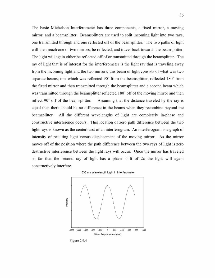
The basic Michelson Interferometer has three components, a fixed mirror, a moving
mirror, and a beamsplitter. Beamsplitters are used to split incoming light into two rays,
one transmitted through and one reflected off of the beamsplitter. The two paths of light
will then reach one of two mirrors, be reflected, and travel back towards the beamsplitter.
The light will again either be reflected off of or transmitted through the beamsplitter. The
ray of light that is of interest for the interferometer is the light ray that is traveling away
from the incoming light and the two mirrors, this beam of light consists of what was two
separate beams; one which was reflected 90˚ from the beamsplitter, reflected 180˚ from
the fixed mirror and then transmitted through the beamsplitter and a second beam which
was transmitted through the beamsplitter reflected 180˚ off of the moving mirror and then
reflect 90˚ off of the beamsplitter. Assuming that the distance traveled by the ray is
equal then there should be no difference in the beams when they recombine beyond the
beamsplitter. All the different wavelengths of light are completely in-phase and
constructive interference occurs. This location of zero path difference between the two
light rays is known as the centerburst of an interferogram. An interferogram is a graph of
intensity of resulting light versus displacement of the moving mirror. As the mirror
moves off of the position where the path difference between the two rays of light is zero
destructive interference between the light rays will occur. Once the mirror has traveled
so far that the second ray of light has a phase shift of 2π the light will again
constructively interfere. 633 nm Wavelength Light in Interferometer
Mirror Displacement (nm)
-1000 -800 -600 -400 -200 0 200 400 600 800 1000
Inte
nsity
Figure 2.9.4

37
If light of more than one wavelength is traveling through the interferometer then a phase
shift of 2π will not occur at the same mirror displacement for each wavelength and a
graph of intensity versus mirror displacement starts to take the shape of a typical
interferogram. 633 nm, 850 nm, 1100 nm, and 1700 nm Wavelength Light in Interferometer
Mirror Displacement (nm)
-4000 -3000 -2000 -1000 0 1000 2000 3000 4000
Inte
nsity
Figure 2.9.5
When all wavelengths of light generated by the source are present the interferogram takes
the shape
Figure 2.9.6
38
Collecting the interferrogram and relating that to mirror displacement is critical to
the operation of an FT-IR system. Small changes in mirror displacement must be
detected, the system must accurately move a mirror a distance of only a few hundred
nanometers. To accomplish such accuracies the FT-IR will send a beam on
monochromatic light along with the IR source beam. This light beam, usually a 633nm
HeNe laser, goes through the same constructive and destructive interference as the IR
light traveling through the interferometer. The mirror is therefore not stepped a certain
distance but is allowed to continuously move back and forth. The points where the HeNe
light completely disappears is referred to as a zero crossing and allows the FT-IR system
to accurately determine the position of the moving mirror. It is at this point that an
analog-to-digital converter inside the system reads the signal level on its detector and
stores it. This interferogram will now be discrete-time Fourier Transformed which
converts this mirror-distance versus signal graph to a frequency versus signal graph.
• Section 2.9.2 Characterization using Ellipsometry
Ellipsometry is a powerful tool using polarized light to study thin films and a
materials surface [15]. By studying the polarization of light that is reflected off a surface,
information can be gained about the properties of the reflective surface if the original
polarization of the light was known. A plane electromagnetic wave traveling in the z-
direction can be described by the equation [13]
+−−= ζ
λπ )(2sin),( vtzEtzE o Equation 2.9.5
where λ = wavelength of the wave v = velocity of wave Eo = wave amplitude ξ = phase Looking down the z-axis at the x-y plane the electromagnetic wave appears as shown in
figure 2.9.7,

39
Figure 2.9.7
which is called linearly polarized light. If the angle of the linearly polarized
electromagnetic wave does not fall on one of the axes we have arbitrarily chosen as our
coordinate system then the wave can be broken into Ex and Ey components.
Figure 2.9.8
Although broken into two different waves, these waves represent one linearly polarized
traveling wave and are in-phase and traveling in the same direction.
When two or more waves are traveling in the same direction but do not share
common amplitude or phase elliptically polarized light occurs.

40
Figure 2.9.9
When linearly polarized light reflects off an interface a change in the polarization
direction may occur. For samples with multiple interfaces such as a thin film on a
substrate, light will be reflected off of those interfaces with different phases and
amplitudes and will sum to form an elliptically polarized light wave. Studying the shape
of this ellipse is the theory of ellipsometry.
The two linear components of the incident light use in ellipsometry are referred to as s-
polarized (perpendicular to plane of incident) and p-polarized (parallel to the plane of
incidence). At angles other than 0˚ and 90˚ the reflection of s-polarized light and p-
polarized light will not be the same. The reflection coefficients for a bulk substrate are
saas
saasp
nnnnR
θθθθ
coscoscoscos
+−
= Equation 2.9.6
and
ssaa
ssaas
nnnnR
θθθθ
coscoscoscos
+−
= Equation 2.9.7

41
Equation 2.9.10
This ratio is found in the ellipsometer through the equation
( ) ∆== i
s
p eRR
ψρ tan Equation 2.9.8,
ψ being the ratio of the amplitudes and ∆ being the phase difference which the
ellipsometer finds by using the shape of the elliptical light wave returned to the detector
[16].
A reflection will occur for every interface the incident light reaches, when multiple thin
films are added on top of a substrate the overall reflections coefficients can be found by
matrix multiplication of successive layer and interface matrices.
=
111ab
ab
abab r
rt
I Equation 2.9.10
=
β
β
j
j
ee
L0
0 Equation 2.9.11
iii
i nd θλ
πβ cos2
= Equation 2.9.12.
Iab = interface matrix for a-b interface
L = layer matrix βi = phase shift due to ith layer

42
di = thickness of ith layer θi = angle of incidence for light on ith layer ni = index of refraction of ith layer rab = reflection coefficient of ith interface tab = transmission coefficient of ith interface In many instances the index of refraction has a complex component. This
component is directly related to the amount of power absorbed by the material per unit
time and unit volume, or loss. Although often the real and imaginary components of the
index of refraction are considered independently they are not. The Kramers-Kronig
method relates the these two values using the equations [17]
∫∞
−=
022
21 '
')'('2)(ωω
ωωωπ
ω dff Equation 2.9.13
and
∫∞
−=
022
12 '
')'(2)(ωω
ωωπ
ω dff Equation 2.9.14
where
f(ω) = f1(ω) + if2(ω) = ε(ω)/ εo -1 Equation 2.9.15
This is important in optical measurements where the material has a large absorption
value, as n will show a strong dependence on the Kramers-Kronig relation.
For a structure which has multiple layers the number of variable that need to be
solved for becomes too large to accurately determine the value for each variable. Instead
of solving for unknowns, modeling software requires the operator to create a model of
what the structure most likely resembles, the software does not solve for a value but
simply performs a regression analysis on the model the user has created to determine the
most accurate values based on the data it has collected.
Because the values determined by the ellipsometer are found from a mathematical
model some type of regression analysis must be performed to optimize the model. The
regression analysis attempts to bring to zero the mean square error (MSE) between the

43
experimental data and the data from the model. The MSE value is calculated from the
function
∑= ∆
∆−∆+
−−
=N
i
iiii
MNMSE
1
2
exp
expmod2
exp
expmod
21
σσψψ
ψ
Equation 2.9.16
N = number of wavelengths M = number of unknowns in model σ = standard deviation of experimental data points
Solving the model requires reducing this value to its absolute minimum; several
methods area available to accomplish this minimization [12]. Although several more
advanced algorithms are known, many of them are derived from the gradient method
which views the MSE as surface in M-dimensional space. The gradient of the MSE
surface is a vector with M components. To move along the gradient, and towards the
minimum value, all components of this vector are modified by some multiple of the
gradient.
The degree to which an operator can trust the values solved for by the
ellipsometer modeling software depends on how much the operator knew about the
sample beforehand. Ellipsometric modeling software includes several options which
place constraints on the models parameters. A common technique in spectroscopic
ellipsometry is to force the model to fit the parameters not at every wavelength but for
parameters of a functional based model. For dielectric thin films a common functional
based model is the Cauchy model which assumes that the real and imaginary portions of
the index of refraction decrease with wavelength based on the functions
42 λλnn
nCBAn ++= Equation 2.9.17
and λkB
keAk −= Equation 2.9.18.
Instead of solving for n and k values at every wavelength the modeling software will
solve only for An, Bn, Cn, Ak, and Bk.

44
More advanced modeling options are available in modeling software which can
be used to study surface morphology and interdiffusion of thin films. The Effective
Medium Approximation (EMA) model is used in many instances when a material is
composed of two or three different materials. The simplest form is the linear
approximation method
CCBBAA fff εεεε ~~~~ ++=
where Aε~ , Bε~ , and Cε~ are the complex dielectric functions of the materials and fA, fB, and
fC are the fractions of the mixed materials. ε~ is the resulting dielectric function.
Although not extremely accurate, the algorithm is often used for quick calculations.
More computationally expensive methods such as the Maxwell-Garnett and Bruggemann
EMA’s are commonly seen in model software packages.
Thin films less than 10 nm are considered “very thin films” and are more difficult
to characterize in ellipsometry [18]. Although still very sensitive to the thin film itself, a
correlation between index of refraction and thickness is present at these thickness and it is
impossible to determine both by ellipsometry alone without some assumption being
made. A graph of the ψ and ∆ values for a film between 10 to 80 nm and indexes of 1.46
to 2.2 on a silicon wafer it can be seen that these values are very sensitive to the 10 nm
film, especially the phase difference coefficient which has changed almost 30 degrees
between the silicon wafer and the silicon wafer with the 10 nm oxide layer.
Figure 2.9.11

45
For thicknesses above 10 nm a unique solution is available for all the different
thicknesses and indexes. Unfortunately no unique solution is available at the 10 nm
thickness for the various indexes and it is generally not possible to distinguish between
correct and incorrect optical constants for very thin films. The most useful solution in
these instances is to use the most accurate optical constants available and then fit for an
“effective thickness.” The “effective thickness” will have some error due to the error in
the optical constants but will be reproducible and give good results when relating the
thickness of one film to the thickness on another.
Chapter Three - Experimental
• Section 3.1 Silicon Dioxide from Electron-Beam Deposition
The first component of my research was the characterization of silicon dioxide
thin films grown from the Temescal BJD-2000 electron gun deposition chamber. Our
goal was to grow SiO2 layers with reproducible refractive indices and thicknesses as well
as stability to environmental conditions. For simplicity the initial characterization of the
layers was performed by depositing the SiO2 onto silicon wafers. Wafers were degreased
in acetone for five minutes and then in methanol for five minutes. To remove any native
oxide the wafers would then be etched in a 1:1 H2O:HF solution and then rinsed in H2O
for 30 seconds. The wafers would then be loaded directly into the deposition chamber
and pump down would begin.
Experiments were conducted after a pump down of more than eight hours. The
wafer holder was rotated at 20 rpm and depositions occurred at 10.00 kV ± 0.04 kV
accelerating voltage using 99.999% purity SiO2 source material which was refilled after
each deposition. Over fifty samples where performed in this way over the course of

46
several months in an attempt to understand the growth conditions that most affected the
deposited SiO2 films. The standard operating procedure was a pressure of 3.3x10⁻⁷ torr,
70 mA emission current to a thickness deposition of 1 µm. Most samples where grown
using this method in an attempt to determine the repeatability of the system but in several
depositions we deviated from these parameters to see what effect this would have on the
films. Index of Deposited Silicon Dioxide Film vs Emission Current
Emission Current (mA)62 64 66 68 70 72 74 76 78 80 82
Inde
x
1.450
1.455
1.460
1.465
1.470
1.475
Figure 3.1.1
Chamber Pressure vs. Index of Deposited Film
Pressure (torr)
1.0e-7 1.5e-7 2.0e-7 2.5e-7 3.0e-7 3.5e-7 4.0e-7 4.5e-7
Inde
x
1.450
1.455
1.460
1.465
1.470
1.475
Figure 3.1.2

47
Thickness of Silicon Dioxide Films vs Index of Films
Thickness (microns)
0.5 1.0 1.5 2.0 2.5 3.0
Inde
x
1.450
1.455
1.460
1.465
1.470
1.475
Figure 3.1.3
Sample Index @ 633nm
032 1.4754
033 1.4780
047 1.4739
050 1.4742
074 1.4544
075 1.4486
Std. Dev 0.0125
Table 3.1.1
No obvious trend came out of any of these plots. In addition to these parameters
we also looked at less obvious criteria such as runs since cyropump regeneration and
relative humidity the day the samples was loaded, and the amount of material on the
chamber walls but attempts to relate these parameters to the index of refraction where
never successful.
The infrared spectrum of silicon dioxide provided a great deal of information
about the stoichiometry and stress in the films [19]. Specifically the Si-O in phase stretch

48
peak located around 1080 cm-1. A good reference for SiO2 material was the spectrum
collected from a thermally oxide wafer.
Figure 3.1.4
A thermally grown oxide that is fully relaxed will have a O-Si-O bond angle of
144.7˚, a Si-Si distance of 1.60Å, and a Si-O in phase stretch located at 1078.5 cm-1. It is
well know that the Si-Si distance and bond angle are related to the strain in the film while
these parameters are related to the location of the Si-O in phase stretch. The reason for
the strain in the films is questionable but is often attributed to a film stoichiometry of less
than 1:2 in SiO2.
While performing FTIR studies on the SiO2 samples it became clear that a shift
was occurring in the Si-O in phase stretch over time. This effect would be harmful for
the biosensor as stability in the environment is a key criteria.

49
Figure 3.1.5
These three scans of the same sample taken at 0 hours (1057.893 cm-1), 24 hours
(1062.711 cm-1), and 48 hours (1070.046 cm-1) after they were removed from the
deposition chamber show that strain in the film is decreasing as the Si-O in-phase stretch
moves closer towards its nominal value of 1078.5 cm-1. There were several possibilities
as to why this was occurring: oxidation of the films from O2 in atmosphere, water
absorption or desorption from the film, or and a natural relaxation of the SiO2 molecules
over time were all considered. In an attempt to study this, three samples where grown in
the e-beam chamber during one deposition at 5 nm ± 0.5 nm per second, 3.3 x 10⁻⁷ torr,
and substrate temperature of 200 ˚C. FTIR scans were taken in transmission mode at a
resolution of 1 cm-1 with a liquid nitrogen cooled MCT detector and an average of 64
scans. Sample A, a reference sample, was removed and taken directly to the FTIR and
ellipsometer for study, sample B was placed into a beaker of deionized water for one hour
before being taken to the FTIR and ellipsometer for study, and sample C was left inside
the vacuum chamber for 47 hours before it was removed and taken to the FTIR and
ellipsometer for study.

50
Sample A Change Over Time
Time (hours)
0 10 20 30 40 50
Thic
knes
s (n
m)
935
940
945
950
955
960
965
970
975
Pea
k Po
sitio
n (c
m-1
)
1054
1056
1058
1060
1062
1064
1066
1068
1070
1072
1074
ThicknessPeak PositionFit
Figure 3.1.6
Sample A and Sample B Si-O Peak Change Over Time
Time (hours)
0 10 20 30 40 50
Peak
Pos
ition
(cm
-1)
1054
1056
1058
1060
1062
1064
1066
1068
1070
1072
1074
Sample A (in atmosphere)Sample B (exposure to water for 1 hour)
Figure 3.1.7
Sample A and Sample B Thickness Change Over Time
Time (hours)
0 10 20 30 40 50
Thic
knes
s (n
m)
930
940
950
960
970
980
Sample A (in atmosphere)Sample B (exposure to water for 1 hour)
Figure 3.1.8

51
The behavior of A showed that a release in strain inside the film was strongly related to
an increase in the thickness of the films, in this case about two percent.
Relating B to A it was seen that the deionized water had accelerated the aging
effect.
Sample A and Sample C Thickness Change Over Time
Time (hours)
0 10 20 30 40 50 60
Thic
knes
s (n
m)
935
940
945
950
955
960
965
970
975
Sample A (in atmosphere)Sample C (in vacuum for 47 hours)
Figure 3.1.9
Sample A and Sample C Si-O Peak Change Over Time
Time (hours)
0 10 20 30 40 50 60
Peak
Pos
ition
(cm
-1)
1054
1056
1058
1060
1062
1064
1066
1068
1070
1072
1074
Sample A (in atmosphere)Sample C (in vacuum for 47 hours)
Figure 3.1.10
C showed the exact opposite trend as B; during the 47 hours inside the vacuum
chamber almost no change in the thickness or the peak location occurred. The small
change that was noticed probably occurred during the time A and B were removed and
the chamber was pumping back down.

52
Another growth using the same parameters as those for samples A, B, and C was
performed. This sample, D, was capped with a 95 nm layer of Al2O3 before removal
from the chamber. It was scanned immediately after removal and then again scanned
seven days later. After this scan the D was placed in deionized water for four hours and
then scanned again. These three scans are all within the 1 cm-1 resolution they were
collected at (1044.858 – 1045.514 cm-1) and no shift can be found during this period.
The fourth scan was collected 100 days later, its location was found to be 1052 cm-1.
This shift was attributed to a release in the stain of the film over time which occurred at a
rate much slower than the rate of a SiO2 film exposed to atmosphere.
Figure 3.1.11
The final thing that the experiments attempted to prove was that this process is
irreversible. A new sample, E, was grown with the same deposition conditions as A
through D. E was allowed to age exactly as A had up until day 15. At day 15 E was
placed back into the e-beam vacuum chamber and pumped down to 2.7 x 10⁻⁷ torr for
three days. After E was removed scans were performed in an attempt to witness reversal
of the process and a shift of the peak away from its nominal position. Although a small
negative shift was noticed between day 15 and day 18 this shift was within the 1 cm-1
resolution of the scan and should not be attributed to anything genuine.

53
Sample A and Sample E Change Over Time
Time (days)
0 2 4 6 8 10 12 14 16 18 20 22
Peak
Pos
ition
(cm
-1)
1071
1072
1073
1074
1075
1076
1077
1078
1079
Sample E (placed in vacuum between days 15 to 18Sample A (left in atmosphere)
Figure 3.1.12
Determining the reason for these shift and thickness changes was the key to
stopping them. Some work has related this process to the water in atmosphere creating
Si-OH bonds from strained Si-O bonds and then reverting back to Si-O bonds which are
less strained [20]. Others have attributed the strain to water inside the films, desorption
of water over time from the film allows it to relax [21]. Clearly in the case of e-beam
grown SiO2 films, desorption of water from the film did not cause relaxation, on the
contrary the presence of water accelerated the process.
• Section 3.1.1 Silicon Dioxide Depositions with Substrate Heat
Based on the instability seen in the SiO2 films it was believed that the films grown
were very porous. A more dense film would most likely stop or slow the absorption of
water into the films. While annealing the films after deposition would increase the
density of a porous film, post-deposition annealing can cause cracking when vapor inside
the film expands. For higher quality film growth, elevated substrate temperatures are
used. This allows surface molecules to diffuse around on the surface and fill any pits that
have occurred on the film surface.
The equation

54
RTE
r
oos seJ
na 2/−=Λν Equation 3.1.1
provides a mathematical model explaining why higher substrate temperatures provide
better film quality. The diffusion length, Λ, of the molecule is related to the temperature
of the substrate, T, and the deposition flux Jr. The value vos is the vibrational energy of
the molecule in question, although this value only requires attention when the substrate
temperature is high enough to move the molecule from its ground vibrational state. For
the temperatures used in the e-beam deposition chamber this does not occur and the value
is assumed to be 1013. As the molecule diffuses around the surface it reaches areas of
higher and lower surface energy. The value a is the distance between two sites of lower
surface energy and no is the number of these sites per cubic centimeter.
The density of amorphous silicon dioxide is 2.97 g/cm3. To determine the flux
rate for a 10 Å/s deposition we use
322
24
3100.3
1066.160
97.2
cmmcx
amugx
mcamu
cmg
=⋅ −
which is the number of molecules per cubic centimeter. The flux is then
scmmcx
scm
cmmcx
⋅=⋅ −
2147
322 10310100.3 ,
assuming no desorption is occurring. If assuming that a site of least surface energy
occurs at every SiO2 molecule or between SiO2 every molecule, then the number of
surface sites for adsorption is the number of molecules on the surface of the cube used for
molecular density so and the distance between them is 14106.9 xno =
cmxcmx
a 8
3 322102.3
100.31 −== .
Es (around 20 kJ/mol for amorphous SiO2) is the activation energy for surface diffusion
on the SiO2 film surface, this value is always much less than the desorption activation
energy for SiO2 since bonds are only partially broken as the molecule moves around the
surface. R is the gas constant 0.00831 J/mol·K and varying T between 273 ˚K and 573
˚K we find

55
Diffusion Length of Silicon Dioxide as a Function of Substrate Temperature
Substrate Temperature (Kelvin)
250 300 350 400 450 500 550 600
Diff
usio
n Le
ngth
(cm
)
0.000
0.005
0.010
0.015
0.020
0.025
Figure 3.1.13
By increasing the substrate temperature the diffusion length of the SiO2 molecules on the
surface has increased from 0.0022 cm to 0.022 cm. This increased mobility should
produce denser films with higher indexes while also reducing the amount of empty space
within the films for contaminants to reside. This should in turn produce better overall
reproducibility in SiO2 film growth.
The substrate heater gave us one more parameter that could improve film quality.
A “bakeout” is simple taking the chamber to a higher temperature than the deposition will
be performed at in an attempt to remove contaminants from the surface before deposition.
A chamber backout of 290 ˚C for ten minutes before lowering the temperature to 280 ˚C
and starting the deposition allows the chamber pressure to reach pressures lower than it
would have been able to achieve if no bakeout would have been performed.

56
Sample Index @ 633nm
S202 1.4699
S204 1.4669
S206 1.4418
S208 1.4589
S209 1.4690
Std. Dev. 0.0117
Table 3.1.2
• Section 3.1.2 Silicon Dioxide Depositions with Ion Beam Assist
Although the index variations for these samples was still too high for our devices
the use of a substrate heater showed promise. A good rule of thumb for improvement in
deposited films is to use a substrate temperature of one-third the melting temperature of
the material, which for SiO2 is 1713 ˚C. This means a substrate temperature of 571 ˚C
would have been a good starting point when attempting to optimize the SiO2.
Unfortunately the e-beam deposition chamber was only able to operate at temperatures <
300 ˚C. A different method to couple energy into the depositions process was needed.
The addition of the Denton Vacuum CC-105 Cold Cathode Ion Source to the e-
beam chamber for Ion Beam Assisted Deposition (IBAD) allowed us to add many new
deposition parameters, including gas flow into the chamber, drive current of the ions, and
neutralizing current. It is well known that the depositions of dielectrics using an e-beam
chamber produce porous, non-stoichiometric films. The CC-105 ion source can produce
an oxygen ion stream to increase film density and stoichiometry.
The two most important parameters with any ion source flux rate and drive
voltage (VD) which is dependent on the system configuration, drive current, properties of

57
the gas in use, gas flow rate, and background pressure. Although the ion source sets VD
based on the drive current (ID) given by the operator, VD can be changed considerably by
changing these other parameters. Regardless of the operating parameters the quantities of
interest are the energy with which the ions are striking the surface (in eV) and the ion
flux (µA/cm2). The ion source’s distance from the center of the chamber, distance from
substrate holder, and tilt angle all play important roles in determining these two
parameters and ion energy and flux are only determined experimentally.
If ions where allowed to continually strike the substrate a charge would occur and
new ions would begin to be repelled. In addition, a positive charge buildup on the
chamber walls will cause arcing to occur inside the chamber creating electrical noise in
the crystal monitor and possibly tripping the electron guns interlocks. The neutralizing
current (IN) and neutralizing voltage (VN) parameter on the ion source controls the
amount of current that flows through a filament located just above the head of the ion
source and prevents charging from the ions. Electrons enter into the positively charge ion
stream and create an electrically neutral plasma. According to literature and the ion
sources manual this parameter has no effect of film deposition as long as it is high
enough to provide stable ion source and electron gun operation. The user set the IN value
and the ion source would adjust the VN to continually provide the set value. Because the
filament in located directly inside the ion stream its lifetime is very short. When VN
reaches > 19V filament burnout is imminent.
The use of the ion source required us to rethink the deposition parameters used in
the past. The ion source itself produced an appreciable amount of heat which resulted in
a steady rise in substrate temperature during deposition. In an attempt to keep the
chamber conditions constant throughout the depositions a high substrate temperature was
now required. For a typical 1 µm SiO2 deposition at different beginning substrate
temperatures the final substrate temperatures are listed below.

58
Beginning Substrate
Temp (˚C)
Final Substrate
Temp (˚C)
100 157
200 244
260 271
280 282
Table 3.1.3
For the ion source to be effective the deposition rates were slowed. Because the
ion source was off the center axis and the films may not experience the same amount of
ion bombardment at different locations in its rotation a deposition of only a few
monolayers per revolution was required. Failure to do this would have resulted in
alternating layers of different densities inside the film.
Experiments performed to optimize the SiO2 with IBAD growths occurred at a
deposition rate of 3.5 Å/s, chamber bakeout at 290 ˚C for ten minutes, substrate
temperature at deposition of 280 ˚C, chamber pressure of 8.5x10⁻⁵ (which occurred with a
O2 flow rate of 17.5 sccm), rotation of 50 RPM, a neutralizing current of 23.0 A, and a
deposition thickness of 1 µm.
Sample Index @ 633nm
262 1.4637
263 1.4666
Std. Dev. 0.0021
Table 3.1.4
The sample pool was too small to accurately calculate the standard deviation for
SiO2 samples using SiO2 source material and the ion source. The ion source gave us the
ability to deposit samples from silicon source material and reactively deposit SiO2. Only

59
two samples were grown from SiO2 source material before we switched to the reactive
deposition method which is discussed below.
In addition to these characteristics we were also very interested in what would
now happen to the Si-O in-phase stretching peak over time. A denser film which has a
stoichiometry closer to 1:2 for Si:O should be more stable. This was the case for sample
262 whose FTIR spectrum is below.
Figure 3.1.14
Although some variation in the FTIR spectrum was noticed and the Si-O
stretching peaks were still not at their optimal 1078.5 cm-1 peak the ion source made a
great deal of improvement.

60
• Section 3.1.3 Silicon Dioxide Reactive Deposition
A typical e-beam deposition involves sweeping the beam itself around the source
material before deposition begins. The material liquefies and forms a molten pool. Any
contaminants in the source material with a higher vapor pressure will be ejected out and
stick to the shutter. After a melt in period the beam sweep can be slowed, or even
stopped, in the center of the molten pool of source material. Material is evaporated from
the center of the pool forming a small pit and new material from the edge flows in to
replenish this pit. This technique most accurately represents the model used to
characterize and build e-beam chambers, line-of-sight deposition from a point source.
Depositing silicon dioxide using an e-beam chamber is considerably different from this
ideal case. The thermal characteristics for SiO2 prevent the material from entering into
the liquid phase during deposition, the top layer of SiO2 pellets will fuse together but will
not form a molten pool. Deposition flux will fluctuate throughout the deposition as the
beam encounters the void between source pellets. In addition the flux change will not be
the same for all directions inside the chamber. This introduces error into the correlation
between the stationary thickness monitor and the rotating substrates.
A solution to this is to use silicon metal, which does form a molten pool when
heated with the e-beam, and perform a reactive deposition with oxygen ions. These
depositions where performed at 3.5 Å/s, a chamber bakeout at 290˚C and deposition at
280˚C, 50 RPM substrate rotation, 23.0 A neutralizing current, 2.25 A drive current, 144
V drive voltage, 17.5 sccm O2 flow which forced a chamber pressure of 8.5x10⁻⁵. This
technique produces more accurate thickness than the depositions performed from SiO2
source material but I do not feel that enough depositions performed from SiO2 using
similar parameters have been performed to make a mathematical comparison.
Although the depositions from SiO2 with the use of the IBAD produced FTIR
spectrum showed very little strain inside the films, it appears that the reactive method
produced even less stress inside the films.

61
Figure 3.1.15
In addition no peak shift has been detected in the reactively grown SiO2 while samples
from SiO2 source with IBAD did move slightly over the course of several months.
Sample Index
283 1.4768
284 1.4794
287 1.4742
315 1.4762
Std. Dev. 0.0021
Table 3.1.5
• Section 3.2 Sweep Pattern Selection
As discussed before, silicon dioxide material can be difficult to evaporate due to
the inability to create a molten pool of source material. It is therefore necessary to create
a sweep pattern that will continue throughout the deposition and will evaporate from all

62
points on the source material surface equally. If this failed to occur, the electron beam
would drill through the source material and begin striking the graphite liner or copper
hearth resulting in contamination or damage to the electron gun itself. Although the gun
sweeper allows the operator to rapidly create new sweep patterns these are usually only
for simple geometries such as circles or figure eight’s.
Figure 3.3.1
Figure 3.3.2

63
Figure 3.3.3
The patterns all assume that the electron beam itself has a constant shape over the entire
pocket which is not the case. The beam itself is focused at the top center of the crucible
and becomes more diffused as it travels away from that position. The designer of the e-
beam chamber, BOC Edwards/Temescal, provided us with a model for a sweep pattern
for subliming materials.
SS-64 sweeping pattern recipe.
-0.200
0.000
0.200
0.400
0.600
0.800
1.000
1.200-1.000 -0.500 0.000 0.500 1.000 1.500
Lateral current, amp. Magnet N pole -->
Long
itudi
nal c
urre
nt, a
mp.
Em
itter
-->
Track#1Track#2Track#3Track#4Track#5Track#6Series7Track#7Track#8
Figure 3.3.4
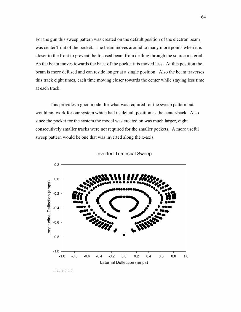
64
For the gun this sweep pattern was created on the default position of the electron beam
was center/front of the pocket. The beam moves around to many more points when it is
closer to the front to prevent the focused beam from drilling through the source material.
As the beam moves towards the back of the pocket it is moved less. At this position the
beam is more defused and can reside longer at a single position. Also the beam traverses
this track eight times, each time moving closer towards the center while staying less time
at each track.
This provides a good model for what was required for the sweep pattern but
would not work for our system which had its default position as the center/back. Also
since the pocket for the system the model was created on was much larger, eight
consecutively smaller tracks were not required for the smaller pockets. A more useful
sweep pattern would be one that was inverted along the x-axis.
Inverted Temescal Sweep
Laternal Deflection (amps)-1.0 -0.8 -0.6 -0.4 -0.2 0.0 0.2 0.4 0.6 0.8 1.0
Long
itudi
nal D
efle
ctio
n (a
mps
)
-1.0
-0.8
-0.6
-0.4
-0.2
0.0
0.2
Figure 3.3.5

65
All eight tracks were unnecessary and only track one (outer most track), track 3, and
track 6 were kept and loaded into the electron guns sweeper. Using the handheld sweep
adjuster, which allowed in-situ adjustments of x and y amplitudes and center positions,
this pattern was fit to the deposition chamber and gave acceptable results but would
occasionally drill through the source material in the back of the pocket if the material was
not densely packed. Adjustments to the beam forming magnets inside the electron gun
itself decreased the focus of the beam towards the back of the pocket and reduced the
amount of drilling even further.
• Section 3.3 Aluminum Oxide from Electron-Beam Depositions
These layers were where the light would be guiding and the ability of the layers to
do so was another characterization criterion that was looked at. These depositions were
initially performed on high pressure oxide (HIPOX) wafers which were cleaned in a five
minutes acetone and five minutes methanol degreasing. In an attempt to achieve an
understanding of the deposition parameters that were affecting the growths we performed
numerous depositions under different conditions. Some trends were clearly seen, such as
the fact that pressure inside the chamber at the beginning of the deposition had an effect
on the resulting index. A lower pressure would result in a longer mean free path and
therefore denser films.

66
Figure 3.3.1
This trend was later found to be irreproducible, although in general a lower pressure
would result in a higher index it appeared there were numerous parameters affecting the
Al2O3 depositions. A study of seven samples grown during the same time period with
pressure between 2.0 – 3.0 x10⁻⁶ torr, deposition rate of 10 Å/s, and substrate rotation of
20 RPM showed a high standard deviation in the refractive indices amongst the films.
Sample Index of Refraction @ 633nm
127 1.6058 129 1.6121 131 1.6184 133 1.6111 135 1.6156 143 1.6461 150 1.6388
Std. Dev. 0.0152
Table 3.3.1

67
Samples 127 through 135 fell in the region expected based on the previous graph. For
unknown reasons some samples, such as 143 and 150, had drastically different indices
even though growth conditions were believed to have remained consistent.
When placed in the prism coupler an Al2O3 film that guided well would show a
streak visible across the entire surface of the substrate.
Figure 3.3.2
No scattering could be seen from contaminates inside the film and the losses appeared to
be small. Unfortunately most of the films produced would not appear like this. Many
were weakly guiding or had a large amount of scattering.

68
Figure 3.3.3 Slight Guiding
Figure 3.3.4 Slight Guiding

69
Figure 3.3.5 Guided well but with scattering
It was rarely possible to see any streak coming from the prism. Parameters such
as chamber pressure, growth rate, source material age, amount of material on chamber
walls, and the relative humidity of the day the sample was loaded were all considered
possibilities for why some samples guided and some didn’t. When no trend could be
found an attempt was made to see if any contamination was present in the films. We
believed that it was possible that carbon from the graphite liners or gold deposited on the
chamber walls from previous depositions was entering into the films. Energy Dispersive
Spectroscopy (EDS) was performed on a sample to see if any contamination was present.

70
Figure 3.3.6
The platinum used to prepare the sample for EDS could clearly be seen as well as the
silicon from the substrate, negligible carbon and no gold was detected.
• Section 3.3.1 Aluminum Oxide Depositions with Substrate Heat
When the ability to perform depositions with substrate heat was added to the
system new depositions were performed to characterize the system and attempt to bring
greater index reproducibility and increased guiding by the samples. Using a selection of
samples deposited on degreased borofloat glass wafers at pressures between 2.3 – 2.9 x
10-6 torr, 290˚C substrate temperature, and a deposition rate of approximately 10 Å/s we
saw a decrease in the standard deviation in refractive indices when compared to those
performed without substrate heat.

71
Sample Index @ 633nm
243 1.6599
251 1.6519
254 1.6522
249 1.6539
Std. Dev. 0.0037
Table 3.3.2
Comparing these samples with those without the substrate heater we saw that the mean
index of refraction for samples had increased from 1.6211 to 1.6545. On occasion
samples produced with deposition parameters thought to be exactly the same as the
samples listed above would produce indices considerable different from the mean, such
as sample 242 which had an index of refraction of 1.6924. No explanation could be
found for why this was occurring.
With the addition of the thermocouple that was installed with the substrate heater
it was possible to monitor chamber temperatures during a deposition without the use of
substrate heat. During a typical eight minute deposition of Al2O3 material the
temperature of the substrate would rise to over 200˚C due to radiation from the hot source
material. The effect on depositions that the substrate heater was having on the new
samples was also occurring in samples without substrate but not until well into the
deposition. Ellipsometric graded index measurements on a sample with and without
substrate heat showed the effect.

72
Effect of Heat on Depositions
Distance from Substrate
0 50 100 150 200 250
Inde
x of
Ref
ract
ion
1.610
1.615
1.620
1.625
1.630
1.635
1.640
With Substrate HeatWithout Substrate Heat
Figure 3.3.7
Although the effect of heat on the deposition could clearly be seen, it was puzzling that
the index of refraction of the material was going lower as the substrate temperature rose.
This was counterintuitive since the substrate heat would create a denser material with a
higher index of refraction. This could be explained by outgassing of contaminates from
the chamber walls as the chamber heated up or that the morphology of the film at low
temperatures promoted porous film growth throughout the deposition.
The effect of substrate heat on the guiding of the Al2O3 films was poor. For all
the aluminum oxide samples that were produced with substrate heat (samples 202 to 260)
only two were considered to “guide well.” The fact that the number of samples that
guided with substrate heat was lower than the percentage that guided without the
substrate heater it was unlikely the inability of the films to guide was due solely to the
density of the films. Having previously ruled out contamination as a possibility it now
seemed that the loss of an oxygen atom from the Al2O3 molecules was the most likely
cause of the poor guiding. EDS on a sample grown with the substrate heat showed a
trend of less oxygen and more aluminum with greater incident electron energy
(corresponds to a greater penetration depth).

73
Figure 3.3.8
• Section 3.3.2 Aluminum Oxide Depositions with Ion Beam Assist
The improvements on the Al2O3 films with IBAD were evident with the first several
samples produced. A streak was clearly seen for every Al2O3 film deposited which was
thick enough to include a guiding mode.
Figure 3.3.9 Sample 263

74
Regardless of the operating parameters of the ion source the Al2O3 film would guide. It
was not possible to visually detect a difference in the losses of the films when comparing
one set growth parameters to another. Research now focused on characterization of the
ion source to find the operating parameters that would give the most consistent index
with the greatest amount of moisture stability.
These experiments were performed on borofloat wafers which were soaked and
sonicated in acetone for five minutes and then soaked in methanol for five minutes.
Samples were loaded into the chamber and the substrate heater was set to 290˚C for one
hour. After one hour the substrate heater was turned off and the chamber continued to
pump down for an additional two hours. After this time the substrate heat was turned
back on and set to 200˚C which it reached in about seven minutes. At this point pressures
were between 6.0 to 6.2 x10⁻⁶ torr. An oxygen flow rate of 17.5 sccm was set and
neutralizer current was set to 23.0 amps. The drive current was varied among the
experiments (between 1.25 to 2.5 amps) to see what range of refractive indices the system
was capable of achieving. After thirty seconds to one minute the chamber pressure
would reach equilibrium around 8.2 – 8.6 x10⁻⁵ torr and the depositions would begin.
Under computer control the electron-gun would soak the source material for thirty
seconds at 22% power (1.3kW) and then lower to 17% power (1.0kW) to soak for
another thirty seconds. The shutter would then open and the deposition rate would be 3.5
± 1.5 Å/s. The system would automatically adjust the emission current from the electron
gun to maintain a 3.5 ± 0.2 Å/s deposition rate.

75
Depositied Alumina Film Indices Based on Various Drive Currents
Drive Current (amps)
1.0 1.2 1.4 1.6 1.8 2.0 2.2 2.4 2.6
Inde
x of
Ref
ract
ion
1.59
1.60
1.61
1.62
1.63
1.64
1.65
Figure 3.3.10
The typical index refraction for aluminum oxide is around 1.63 at 633 nm,
therefore a drive current of 2.25 amps was chosen as the optimal value for future
depositions. Several single layer films were produced with the previous deposition
parameters but now holding the drive current to 2.25 amps. Before the beginning of the
experiment the e-beam chamber was cleaned and new source material was loaded.
Before each new deposition small amounts of source material would be added to
replenish what had been used.

76
Increased Index Reproducibility based on Material Usage
Material Evaporated to Chamber Walls (nm)0 200 400 600 800 1000 1200 1400
Inde
x of
Ref
ract
ion
1.626
1.628
1.630
1.632
1.634
1.636
1.638
1.640
1.642
1.644
Figure 3.3.11
The first three samples produced showed large amounts of standard deviation in the
refractive indices, σ = 0.0062, while the next five samples showed a significant decrease
in standard deviation to σ = 0.00057. This result proved that chamber wall and source
material conditioning were important for reproducible results and that source material
should not be replaced with every deposition but only replenished as needed.
Sample Index
292 1.63390
293 1.63470
294 1.63390
295 1.63340
296 1.63470
Std. Dev 0.00057 Table 3.3.3

77
• Section 3.3.3 Aluminum Oxide Moisture Stability
The biosensor device will be working in an aqueous solution and the moisture
stability of the samples was of considerable concern. The stability of the films,
specifically the top aluminum oxide layer, depends on how much water can enter into the
pours of the films and the population of –OH groups; films with higher indices should be
denser, have less film surface area, and therefore show less of a change when exposed to
water [22, 23]. To test how the films changed when exposed to water several growths
were performed at several different ion drive currents. Cleaned borofloat samples were
loaded into the chamber and heated to 275˚C for five minutes. After this the heat was
turned off and the chamber pumped down for three hours. After the pump down the
substrate heat was turned back on to 200˚C and the oxygen flow rate was set to 17.5
sccm; the pressure would be between 8.7-9.1x10⁻⁶ torr. Substrate rotation was set to 20
RPM and depositions occurred to a thickness of 140 nm and at rate of 3.5 ± 0.2 Å/s.
After completion the chamber was allowed to cool for over two hours so the
temperatures would reach below 75˚C. When removed the samples were taken to the
ellipsometer and thickness and refractive index measurements were taken. The samples
would be soaked in deionized water for 20 minutes and dried just enough to remove any
remaining water from the surface. Ellipsometry measures were again taken.

78
Alumina Instability due to H2O
Ion Drive Current (amps)
1.0 1.2 1.4 1.6 1.8 2.0 2.2 2.4 2.6
Inde
x
1.610
1.615
1.620
1.625
1.630
1.635
1.640
1.645
Index before 20 minute H2O DipIndex after 20 minute H2O Dip
Figure 3.3.12
Index Shift after 20 minute Deionized Water Soak
Ion Drive Current (amps)1.0 1.2 1.4 1.6 1.8 2.0 2.2 2.4 2.6
Del
ta n
-0.004
-0.002
0.000
0.002
0.004
0.006
0.008
Figure 3.3.13
As expected the increased drive current produced films with higher indices due to the
higher densities. Although the ∆n’s were most likely within the limits of the
ellipsometer, measurements consistently showed a change refractive index after the water

79
soak and a decrease in ∆n with higher drive currents. Although aluminum oxide is
considered to be one of the most moisture stable dielectrics it was unexpected that so
little of a change was seen in the samples grown at lower drive currents. It was possibly
that the water was leaving the film quickly and that very little was left once the sample’s
surface had dried and ellipsometer measurements were taken the second time.
K Value Shift due to Moisture Instability of Alumina
based on Ion Source Drive Current
Drive Current (amps)
1.0 1.2 1.4 1.6 1.8 2.0 2.2 2.4 2.6
log
(k)
1e-8
1e-7
1e-6
1e-5
1e-4
1e-3
1e-2
1e-1
K values before water soakK values after water soak
Figure 3.3.14
Delta k based on Ion Source Drive Current
Ion Drive Current (amps)
1.0 1.2 1.4 1.6 1.8 2.0 2.2 2.4 2.6
log
(del
ta k
)
1e-7
1e-6
1e-5
1e-4
1e-3
1e-2
Figure 3.3.15

80
Again the data shows what was expected from films with higher drive currents. The k
values ( n ikn +=~ ) were decreasing with higher energies while the ∆k’s were also
becoming smaller.
Relative k Shift due to Moisture Instability based on Ion Source Drive Current
Ion Drive Current (amps)
1.0 1.2 1.4 1.6 1.8 2.0 2.2 2.4 2.6
Rel
ativ
e k
Shift
0.4
0.5
0.6
0.7
0.8
0.9
1.0
1.1
Figure 3.3.16
The relative shifts
−
initialfinalinitial
were seen to be increasing with drive current, k
values were increasingly sensitive to the presence of water when losses reached minimal
values in the high quality alumina films.
• Section 3.4 Structure Growth
Having resolved many of the chemical and optical issues involved with the
depositions the research focused on growing the waveguide structures with the greatest
amount of thickness control possible.

81
Figure 3.4.1
• Section 3.4.1 Thickness Control Measurements
To test the limits of the quartz crystal deposition monitor eight depositions were
performed. These samples were on borofloat wafers that were soaked in acetone and
sonicated for five minutes then soaked in methanol for five minutes. Samples were
loaded in the chamber and after the cryopump was opened the substrate heat was turned
on and allowed to reach 290˚C. After one hour at 290˚C the substrate heat was lowered
to 260˚C and the ion source was started with an oxygen flow of 17.5 sccm, neutralizer
current of 23.0 amps, and drive current of 2.25 amps. After allowing one to two minutes
for the pressure to stabilize the deposition process started. The material was melted in
with a soak power of 22% (1.3kW) for thirty seconds and then a soak power of 17%
(1.0kW) for thirty more seconds. After completion the shutter opened and the deposition
monitor controlled the emission current to maintain a 3.5 ± 0.2 Å/s deposition rate until a
thickness of 144 nm had been reached.

82
Ellipsometer Measured Thickness of 144nm Deposition Based on Crystal Usage
Crystal Usage (Precent)2 3 4 5 6 7 8 9
Thic
knes
s (n
m)
144
146
148
150
152
154
Figure 3.4.2
The first two runs performed using the new crystals were within 0.3nm of each
other (145.52nm and 145.28nm) and were within the error bars for the ellipsometer. If
this accuracy continued then retooling the crystal monitor would mean future depositions
would be within 0.3nm of 144nm. The data showed that after the second deposition the
accuracy of the crystal monitor degraded and the eight samples had a standard deviation
of 2.95 nm.
Although the crystal monitor closed the deposition shutter at 144 nm the display
continued to fluctuate for several minutes after deposition. This did not result from any
deposition or flaking of material onto/off of the crystal but due to stress change,
absorption of vapor, or change in vibrational modes of the crystal during cool down. For
this reason it was imperative that the temperature of the crystal monitor stay constant
during deposition.
The thickness reported by the crystal monitor at the end of the deposition
increased (after cool down) with each deposition.

83
Crystal Monitor Thickness Reading After Chamber Cool Down
Crystal Usage (Percent)
2 3 4 5 6 7 8 9
Thic
knes
s (n
m)
150
152
154
156
158
160
162
Figure 3.4.3
This was a good indicator that there was a problem with the crystal monitor’s ability to
adapt to the increase in heat it was experiencing during depositions. Since the ion source
and substrate heaters were running for several minutes before the depositions started the
most likely cause was the sudden surge of radiation the crystal experienced as soon as the
deposition shutter was opened. To test this, a run was performed in which the electron
gun current was high enough to turn the aluminum oxide molten but too low to vaporize
the material. The crystal used had one previous deposition on it, 170nm of Al2O3. When
the shutter opened the crystal monitor should not have reported any change.
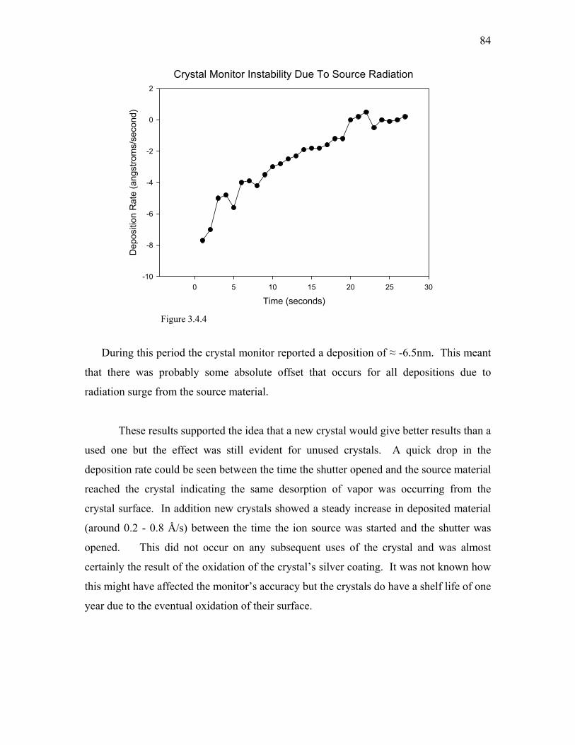
84
Crystal Monitor Instability Due To Source Radiation
Time (seconds)0 5 10 15 20 25 30
Dep
ositi
on R
ate
(ang
stro
ms/
seco
nd)
-10
-8
-6
-4
-2
0
2
Figure 3.4.4
During this period the crystal monitor reported a deposition of ≈ -6.5nm. This meant
that there was probably some absolute offset that occurs for all depositions due to
radiation surge from the source material.
These results supported the idea that a new crystal would give better results than a
used one but the effect was still evident for unused crystals. A quick drop in the
deposition rate could be seen between the time the shutter opened and the source material
reached the crystal indicating the same desorption of vapor was occurring from the
crystal surface. In addition new crystals showed a steady increase in deposited material
(around 0.2 - 0.8 Å/s) between the time the ion source was started and the shutter was
opened. This did not occur on any subsequent uses of the crystal and was almost
certainly the result of the oxidation of the crystal’s silver coating. It was not known how
this might have affected the monitor’s accuracy but the crystals do have a shelf life of one
year due to the eventual oxidation of their surface.

85
• Section 3.4.2 Ellipsometer, Prism Coupler, and Simulation Results
It becomes increasing difficult to accurately measuring the refractive indices and
thicknesses of films when multiple films are present. In an attempt to determine the
accuracy of the ellipsometers’ measurements of multiple layer structures the data that was
collected from several structures was modeled in CAD software to determine the
locations of the two guided modes that should occur in the structures. The actual
locations were then determined by the use of a prism coupler.
Buried Guide
(nm) Oxide (nm)
Top Guide (nm)
PC Mode 1
PC Mode 2
Sim. Mode 1
Sim. Mode 2
Mode 1 Error
Mode 2 Error
154.6 1082 193.8 1.4923 1.5159 1.4889 1.5111 0.0034 0.0048 154.8 1129.5 194.4 1.4905 1.5148 1.489 1.5112 0.0015 0.0036 177.3 1138.6 232.2 1.5122 1.5253 1.5059 1.519 0.0063 0.0063 170.7 1114.7 240.2 1.5179 1.5246 1.5059 1.5168 0.012 0.0078 196.1 990.4 263.8 1.5253 1.5308 1.5187 1.5256 0.0066 0.0052
Table 3.4.1
Mode error, the difference between prism coupler actual locations and where simulations
say the location should be based on the data collected from the ellipsometer, was within
the error tolerances of the ellipsometer. This is due to the numerous factors that come
into effect when multiple films are present, such as surface roughness and intermixes.
Changing model options will produce changes in the values solved for by the
ellipsometer. A typical result would involve measuring the first two layers thicknesses
during the mask change before the top aluminum oxide deposition; after the completion
of the third layer the values obtained are used as the base for the full model. Sample
B327AOA showed a film stack with the parameters,
Figure 3.4.5

86
an alumina index of 1.639, and a silicon dioxide index of 1.475. By changing the model
so that the thicknesses of the two underlying layers could be solved for and was not set to
values from a previous measurement the model now solves for the values
Figure 3.4.6
The multiple optical constants are not solved for at the same time. Those that were used
for this model were from previous growths that were single layers on borofloat substrates.
Allowing the model to adjust the optical constant of one layer still provides valid results;
solving for n and k values of the top aluminum oxide layer changed solved values to
Figure 3.4.7
The top alumina layer now has an index of 1.635 as compared to 1.639 before.
It was also possible that some amount of intermix between any two layers was
occurring. The model was adjusted to account for this.
Figure 3.4.8
A 13.9 nm layer of material consisting of 50% aluminum oxide and 50% silicon dioxide
was solved for between the top aluminum oxide and the silicon dioxide layer. No
intermix was found between the bottom aluminum oxide and silicon dioxide layer. This
result suggests some effect occurring due to the vacuum break.

87
Adding surface roughness to the model allowed further adjustments, most notably
an increase in the intermix to 17 nm.
Figure 3.4.9
None of these models were any less valid than any other. Work remains to be done to
develop the correct model so that the most accurate thickness and refractive index
measurements can be obtained.
• Section 3.4.3 Surface Roughness
Before the biolayer was grown on the deposited aluminum oxide films
experiments were performed on crystalline aluminum oxide (sapphire) wafers. Initial
results showed that the atomic smoothness of the sapphire wafers allowed the biolayer
molecules to become more densely packed on the substrate surface as compared to an
amorphous aluminum oxide film. Atomic Force Microscopy (AFM) images showed the
root-mean-square roughness of the deposited films was around 2nm. Decreasing the
surface roughness to the minimum value possible would provide the best conditions for
the biolayer to grow.

88
Figure 3.4.10
A change in the deposition flux to rotation velocity ratio is known to have an
effect on the morphology of thin films. Glancing Angle Depositions (GLAD) is a
technique where a substrate is held at greater than 70˚ and used to grow different three
dimensional structures based on substrate rotation velocity [24]. Experiments have
found that high rotation velocities form more irregular shapes such as helices while low
rotation rates form more densely packed columnar structures.

89
Figure 3.4.11 [25]
Previous depositions occurred at substrate rotations of 50 RPM. To see the effect
of substrate rotation on the surface new depositions were performed at 20 RPM while
keeping all other parameters the same. AFM images showed a decrease in film surface
roughness to 0.63 nm.

90
Figure 3.4.12 Figure 3.4.13
Chapter Four – Conclusion
• Section 4.1 Improvements
Many of the issues hindering the growth of acceptable quality films have been
overcome but good thickness control over the structure growth remains to be resolved.
As more work is done on the growth of the biolayer on the aluminum oxide more work
may be possible to optimize the surface morphology and chemistry for biolayer growth.
• Section 4.2 Improve Thickness Control
Several options to increase the stability of the quartz crystal monitor are available.
Increased cooling from a more powerful water chiller will help alleviate the thermal
shock seen by the crystal head when the shutter is opened. Increased thermal transfer
between the crystal oscillator and the crystal oscillator housing by using a folded piece of

91
gold foil may also help with the thermal instability. If the crystal monitor continues to
show instability which prevents control to less than a few nanometers then in-situ
sputtering of previously grown films may be possible. This would require an intentional
overshoot of the desired thickness for each layer and then removal from the deposition
chamber for ellipsometry measurements. Using heavier argon ions the sputtering of a
few nanometers of the underlying layer before the next layer of the structure is to be
deposited might allow removal of material until the desired thickness is reached.
• Section 4.3 Decrease Surface Roughness
Thorough studies of the effect that long term bombardment of oxygen atoms to the
films surface remain to be done. Ellipsometer measurements have shown that allowing
the ion source to continue bombarding the surface for two to three minutes after the
depositions completes does decrease the surface roughness of the films. Performing
atomic force microscopy measurements on these samples would provide a more
quantitative value for the effect of ion bombardment on surface roughness.
• Section 4.4 Reactive Depositions of Aluminum Oxide from Aluminum Source
Thus far studies of the quality of reactively deposited aluminum oxide films have
shown only that it is possible to produce a guiding film. As seen with silicon dioxide
reactive depositions greater control in thickness and refractive index may be possible
through reactive depositions with aluminum source and oxygen ions.
• Section 4.5
Ion Scrubbing, In-Situ Surface Cleaning
Due to the mismatch in mass between oxygen atoms and silicon dioxide only a
small amount of momentum is transferred when the oxygen ions collide with the

92
borofloat glass. Also due to the oxygen ion’s highly reactive nature an unknown
substance may be forming from contaminates on the substrate surface. If it is found in
the future that surface contamination is a problem, the use of argon ions for in-situ
substrate cleaning by removing a monolayer from the borofloat wafer would be an
option.

Bibliography [1] Turner, Anthony P. F., Biosensors: Past, Present, and Future, Cranfield University, http://www.cranfield.ac.uk/biotech/chinap.htm; (1996) [2] Shull, J., What is a Biosensors?, University of Maryland Baltimore County, http://userpages.umbc.edu/~jshull1/ench772/intro [3] Pathak, S., Resonant Optical Waveguide Biosensor Characterization, Masters Thesis, West Virginia University, (2004) [4] Lloyd, D., Hornak, L., Pathak,S., Morton, D., Stevenson, I., Application of Ion Beam Assisted Thin Film Deposition Techniques to the Fabrication of a Biosensor Chip With Fieldability Potential for Important Biohazard Detection Applications in Society of Vacuum Coaters, 2004 [5] Mahan, John E., Physical Vapor Deposition of Thin Films, Wiley-Interscience Publishing; (2000) [6] Boisde, Gilbert and Harmer, Alan, Chemical and biochemical sensing with optical fibers and waveguides, Artech House Publishers ;( 1996) [7] Hadley, G. Ronald, Wide-angle beam propagation using Padé approximant operators, Optics Letters, Volume 17, Issue 20, 1426-1429 October 1992 [8] Mattox, Donald M., Handbook of Physical Vapor Deposition (PVD) Processing, Noyes Publications; (1998) [9] Smith, Donald L., Thin Film Deposition Principles and Practice, McGraw Hill; (1995) [10] Palais, Joseph C., Fiber Optic Communications, Prentice-Hall Inc.; (1998) [11] Zabeida, J.E., Klember-Sapieha, and Martinu L., Ion Bombardment Characteristics During the Growth of Optical Films Using a Cold Cathode Ion Source [12] Kaufman, Harold R., Robinson, Raymond S., and Seddon, Richard I., End-Hall Ion Source, Journal of Vacuum Science Technology A, Volume 5, Number 4, Pages 2081-2087; (1987) [13] Why Ion Assisted Deposition (IAD)?, Denton Vacuum, Moorestown, NJ 08057, http://www.dentonvacuum.com/news/tech.html

[14] Fourier Transform Infrared Spectroscopy, Ernest Orlando Lawrence Berkeley National Laboratory, http://spectroscopy.lbl.gov/FTIR-Martin/FTIR-Martin_files/frame.htm [15] Guide to Using WVASE32, Documentation for M-2000U Spectroscopic Ellipsometer, J. A. Woollam Company Inc., Lincoln, Nebraska 68508 [16] Ellipsometry Tutorial, http://www.jawoollam.com/tutorial_1.html, J. A. Woollam Company Inc., Lincoln, Nebraska 68508 [17] Sun, R., Fouere, J., Moore, R., and Lifshin, E., Principle and Application of Spectroscopic Ellipsometery – Characterization of Films and Coatings for Optical, Structural, Chemical, and Electrical Properties, http://www.sungj.com/publicationList.jsp [18] Tiwald, Tom, Application Note: Very Thin Films, J.A. Woollam Co. Inc. [19] M. Yoshimaru, S. Koizumi, and K. Shimokawa, Journal of Vacuum Science and Technology A, 15(6), 2915 (1997). [20] Ila Prasad and A. N. Chandorkar, Journal of Applied Physics, 94, 2308 (2003) [21] E. G. Parada, P. González, J. Pou, J. Serra, D. Fernández, B. León, and M. Pérez-Amor, Journal of Vacuum Science and Technology A, 14(2), 436 (1995) [22] Morton, Dale E., and Fridman, V., Measurement and Correlation of Ion Beam Current Density to Moisture Stability of Oxide Films Stacks Fabricated by Cold Cathode Ion Assisted Deposition, Denton Vacuum Inc., Moorestown, NJ 08057, http://www.dentonvacuum.com [23] Morton, Dale E., Blain, J., Hale, J., Optical Monitoring of Thin-films Using Spectroscopic Ellipsometry, Society of Vacuum Coaters, 45th Annual Technical Conference Preceding; (2002) [24] Robbie, K., and Brett, M.J., Sculptured Thin Films and Glancing Angle Depositions: Growth Mechanics and Applications, Journal of Vacuum Science Technology A, Volume 15, Issue 3, 1460 – 1465; (1997) [25] Malac, M., and Egerton, R., Observations of the Microscopic Growth Mechanism of Pillar and Helices Formed by Glancing-Angle Thin-Film Deposition, http://laser.phys.ualberta.ca/~mmalac/chapter5.html