Fabrication of High-Voltage Bridge Rectifier Modules … · PROJECT NUMBER . 5e. TASK NUMBER : ......
24
Fabrication of High-Voltage Bridge Rectifier Modules for Pulse Power Applications by Dimeji Ibitayo, Gail Koebke, Damian Urciuoli, and C Wesley Tipton ARL-MR-0877 September 2014 Approved for public release; distribution unlimited.
Transcript of Fabrication of High-Voltage Bridge Rectifier Modules … · PROJECT NUMBER . 5e. TASK NUMBER : ......
Fabrication of High-Voltage Bridge Rectifier Modules for
Pulse Power Applications
by Dimeji Ibitayo, Gail Koebke, Damian Urciuoli, and C Wesley Tipton
ARL-MR-0877 September 2014 Approved for public release; distribution unlimited.

NOTICES
Disclaimers The findings in this report are not to be construed as an official Department of the Army position unless so designated by other authorized documents. Citation of manufacturer’s or trade names does not constitute an official endorsement or approval of the use thereof. Destroy this report when it is no longer needed. Do not return it to the originator.

Army Research Laboratory Adelphi, MD 20783-1138
ARL-MR-0877 September 2014
Fabrication of High-Voltage Bridge Rectifier Modules for Pulse Power Applications
Dimeji Ibitayo, Gail Koebke, Damian Urciuoli, and C Wesley Tipton
Sensors and Electron Devices Directorate, ARL Approved for public release; distribution unlimited.
ii
REPORT DOCUMENTATION PAGE Form Approved OMB No. 0704-0188
Public reporting burden for this collection of information is estimated to average 1 hour per response, including the time for reviewing instructions, searching existing data sources, gathering and maintaining the data needed, and completing and reviewing the collection information. Send comments regarding this burden estimate or any other aspect of this collection of information, including suggestions for reducing the burden, to Department of Defense, Washington Headquarters Services, Directorate for Information Operations and Reports (0704-0188), 1215 Jefferson Davis Highway, Suite 1204, Arlington, VA 22202-4302. Respondents should be aware that notwithstanding any other provision of law, no person shall be subject to any penalty for failing to comply with a collection of information if it does not display a currently valid OMB control number. PLEASE DO NOT RETURN YOUR FORM TO THE ABOVE ADDRESS.
1. REPORT DATE (DD-MM-YYYY)
September 2014 2. REPORT TYPE
3. DATES COVERED (From - To)
4. TITLE AND SUBTITLE
Fabrication of High-Voltage Bridge Rectifier Modules for Pulse Power Applications
5a. CONTRACT NUMBER
5b. GRANT NUMBER
5c. PROGRAM ELEMENT NUMBER
6. AUTHOR(S)
Dimeji Ibitayo, Gail Koebke, Damian Urciuoli, and C Wesley Tipton 5d. PROJECT NUMBER
5e. TASK NUMBER
5f. WORK UNIT NUMBER
7. PERFORMING ORGANIZATION NAME(S) AND ADDRESS(ES)
U.S. Army Research Laboratory ATTN: RDRL-SED-P 2800 Powder Mill Road Adelphi, MD 20783-1138
8. PERFORMING ORGANIZATION REPORT NUMBER ARL-MR-0877
9. SPONSORING/MONITORING AGENCY NAME(S) AND ADDRESS(ES)
10. SPONSOR/MONITOR'S ACRONYM(S)
11. SPONSOR/MONITOR'S REPORT NUMBER(S)
12. DISTRIBUTION/AVAILABILITY STATEMENT
Approved for public release; distribution unlimited. 13. SUPPLEMENTARY NOTES
14. ABSTRACT
The advancement of wide bandgap semiconductor materials such as silicon carbide (SiC) has made possible devices that exceed the voltage ratings of conventional packages and modules. Therefore, novel high voltage packages and modules must be developed to realize the full potential of these technologies. We report on the fabrication of multiple versions of a 15-kV bridge rectifier module for pulsed-power applications.
15. SUBJECT TERMS
Schottky diodes, solid state rectifiers, semiconductor device packaging, dielectric breakdown
16. SECURITY CLASSIFICATION OF: 17. LIMITATION
OF ABSTRACT
UU
18. NUMBER OF
PAGES
24
19a. NAME OF RESPONSIBLE PERSON
Dimeji Ibitayo a. REPORT
Unclassified b. ABSTRACT
Unclassified c. THIS PAGE
Unclassified 19b. TELEPHONE NUMBER (Include area code)
301-394-5514 Standard Form 298 (Rev. 8/98) Prescribed by ANSI Std. Z39.18

iii
Contents
List of Figures iv
List of Tables iv
1. Introduction 1
2. Module Implementation (Version 1) 1
3. Module Implementation (Version 2) 3
4. Module Implementation (Version 3) 4
5. Conclusions 16
List of Symbols, Abbreviations, and Acronyms 17
Distribution List 18
iv
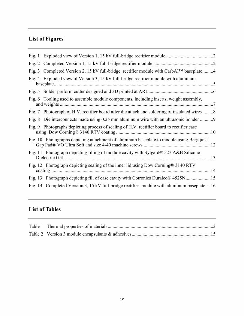
List of Figures
Fig. 1 Exploded view of Version 1, 15 kV full-bridge rectifier module .......................................2
Fig. 2 Completed Version 1, 15 kV full-bridge rectifier module ..................................................2
Fig. 3 Completed Version 2, 15 kV full-bridge rectifier module with CarbAl™ baseplate .........4
Fig. 4 Exploded view of Version 3, 15 kV full-bridge rectifier module with aluminum baseplate .....................................................................................................................................5
Fig. 5 Solder preform cutter designed and 3D printed at ARL ......................................................6
Fig. 6 Tooling used to assemble module components, including inserts, weight assembly, and weights ................................................................................................................................7
Fig. 7 Photograph of H.V. rectifier board after die attach and soldering of insulated wires .........8
Fig. 8 Die interconnects made using 0.25 mm aluminum wire with an ultrasonic bonder ...........9
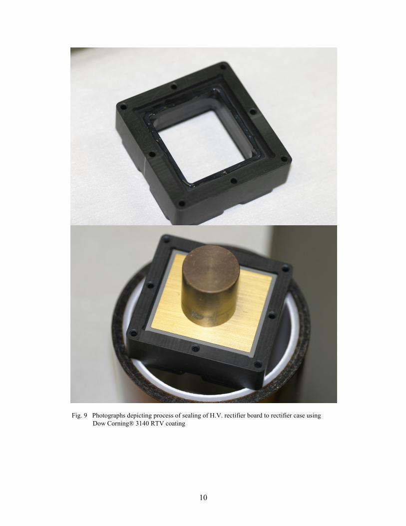
Fig. 9 Photographs depicting process of sealing of H.V. rectifier board to rectifier case using Dow Corning® 3140 RTV coating ...............................................................................10
Fig. 10 Photographs depicting attachment of aluminum baseplate to module using Bergquist Gap Pad® VO Ultra Soft and size 4-40 machine screws ........................................................12
Fig. 11 Photograph depicting filling of module cavity with Sylgard® 527 A&B Silicone Dielectric Gel ...........................................................................................................................13
Fig. 12 Photograph depicting sealing of the inner lid using Dow Corning® 3140 RTV coating ......................................................................................................................................14
Fig. 13 Photograph depicting fill of case cavity with Cotronics Duralco® 4525N .....................15
Fig. 14 Completed Version 3, 15 kV full-bridge rectifier module with aluminum baseplate ....16
List of Tables
Table 1 Thermal properties of materials ........................................................................................3
Table 2 Version 3 module encapsulants & adhesives ..................................................................15

1
1. Introduction
Fifteen-kV full-bridge rectifier modules are a custom component developed and fabricated by the US Army Research Laboratory (ARL) in order to demonstrate 15 kV, 3-A, and 6-A silicon carbide (SiC) junction barrier Schottky rectifier modules in application circuits. Such high voltage, high-speed rectifiers help reduce power conversion volume while increasing efficiency. This development also serves to identify challenges associated with high voltage semiconductor packaging. The SiC junction-barrier Schottky (JBS) diodes used in the module were state-of-the-art devices developed and fabricated by CREE Inc. under the Defense Advanced Research Projects Agency’s Wide Bandgap Semiconductor Technology Initiative. The 3-A rated die are 8 mm × 8 mm in total area, and the 6-A rated die are 10 mm × 10 mm.
2. Module Implementation (Version 1)
Three versions of the 15 kV bridge rectifier modules were fabricated at ARL for various applications. A total of 12 modules have been fabricated to-date, using a multi-step packaging and assembly process. Version 1 (V1) was developed for a 40-kV converter and used the 3-A SiC JBS diodes mounted on a Curamik Electronics aluminum nitride (AlN) direct bond copper (DBC) substrate material (0.3 mm Cu/0.6 mm AlN/0.3 mm Cu). For all versions of the module, the DBC substrate was patterned to meet electrostatic simulation criteria and to accommodate devices, bond wires, and terminals on the top side. An exploded view of V1 is shown in Fig. 1, and a photograph of a completed module is shown in Fig. 2. As shown in Fig. 1, a pocket was cut into the top face of the copper heat sink. The bottom-side copper on the substrate was also removed within the pocket region but remained outside the pocket region to allow for soldering of the substrate to the heat sink. A set of holes was drilled through the heat sink to allow the resulting pocket to be partially filled with encapsulant for high voltage operation following solder bonding.

2
Fig. 1 Exploded view of Version 1, 15 kV full-bridge rectifier module
Fig. 2 Completed Version 1, 15 kV full-bridge rectifier module
Solder bonding at the diode-to-substrate and substrate-to-heat sink interfaces was performed using a single-step process in a vacuum reflow oven to achieve low voiding within the solder. A Sn-Ag-Cu alloy solder was used on both interfaces, and the process temperature profile was tailored to reduce mechanical stress in the final assembly. However, cracks were formed as a result of thermomechanical stresses within the DBC substrate after the soldering process. After the die, substrate, and heat sink were bonded, the die interconnects were made using 0.25 mm aluminum bond wires. Finally, 4 copper terminals were attached to the substrate using a Sn-Pb alloy solder.
The plastic case was constructed from Ultem PEI having a maximum working temperature of 168 °C. In addition to its high temperature rating, this material has a voltage breakdown rating in excess of 20 MV/m and low moisture absorption. The height of the case and terminal locations was specified to provide sufficient separation of all conductors, including the heat sink, to prevent voltage breakdown in air. Grooves were machined into the outside surfaces of the case to mitigate voltage creep. The case was attached to the substrate assembly using room-temperature
Case
Terminals
DBC Substrate
Diodes
Heat sink
Encapsulant

3
vulcanizing (RTV) silicone. Because the module was designed to have the heat sink at a floating potential, the case has 4 threaded holes for module mounting. Similar to the heat sink, a hole was placed in the top of the case to allow approximately three-quarters of the die cavity to be filled with an encapsulant, Dow Corning Sylgard® 527. This product was chosen because encapsulants with high curing temperatures entrapped many voids. The remainder of the cavity was filled with Cotronics Duralco® 4537N epoxy to bind the terminals. The encapsulant was cured under a partial vacuum. Both the encapsulant and epoxy were cured at 27 °C.
3. Module Implementation (Version 2)
The Version 2 module (V2) was developed for the same application as V1 in order to address thermomechanical concerns that arose during the assembly of V1. In the case of V2, a CarbAl™ baseplate was used in place of the copper pin fin heat sink. CarbAl™ is a carbon-based nanocomposite comprised of a 20% dispersed aluminum in 80% carbon. The coefficient of thermal expansion (CTE) of CarbAl™, as shown in Table 1, is significantly lower than that of copper and is a closer match to the AlN DBC substrate and silicon carbide. The cracking of the DBC substrate that occurred in the construction of V1 was not experienced with the change from copper to CarbAl™. CarbAl™ also possesses a high thermal conductivity.
Table 1 Thermal properties of materials
Material Thermal conductivity (W/m⋅K)
Coefficient of thermal expansion (ppm/°C)
SiC 120 3.5–5.0 AlN 185 4.5
Copper 385 16.6 CarbAl-N™ 350–400* 6.60–7.44
*kz, compared to kx, y = 150–200 W/m⋅K A photograph of the completed V2 module is shown in Fig. 3. The DBC substrate was soldered directly to an electroless nickel immersion gold (ENIG) plated CarbAl™ baseplate. Cotronics Duralco® 4525N epoxy was used for binding the terminals due to its lower moisture absorption and higher strength. All of the other materials and processing were identical to what was used in V1.

4
Fig. 3 Completed Version 2, 15 kV full-bridge rectifier module with CarbAl™ baseplate
4. Module Implementation (Version 3)
ARL provided the design and Stellar Industries Corporation was responsible for photo-patterning, copper etching, and electroless nickel immersion gold (ENIG) plating on a Curamik Electronics DBC substrate material (0.3 mm Cu/1.0 mm AlN/0.3 mm Cu). The availability of the thicker ceramic layer allowed for 15 kV operation without the requirement of the dielectric pocket used in the previous 2 versions. Additionally, aluminum was used as the base-plate material, and Gap Pad® VO Ultra Soft was used for heat transfer between the substrate and base-plate in order to dampen vibration. Size 4-40 screws were also used in order to secure the case to the base-plate. Noryl PPO plastic was used instead of Ultem as the case material due to its opacity and reduced cost. Although both plastics have suitable electrical, mechanical, and thermal properties, they are susceptible to stress-cracking in the presence of some common organic compounds such as acetone, gasoline, and kerosene. Both Ultem and Noryl also exhibited stress-cracking when exposed to Loctite 242 Threadlocker®, which was, therefore, eliminated from the module mounting process. As before, the substrate was designed to meet electrostatic simulation criteria and to accommodate devices, bond wires, and wire terminals on the top side. The use of wire terminals extending from the package simplified module fabrication, while effectively eliminating voltage creep at the module case. To reduce strain normal to the substrate, an inner lid was sealed into the case forming an air pocket above the encapsulant to accommodate its thermal expansion. Cotronics Duralco® 4525N epoxy was used to fill the remainder of the open cavity and to bind the wire terminals. An exploded view of the version 3 module is depicted in Fig. 4.
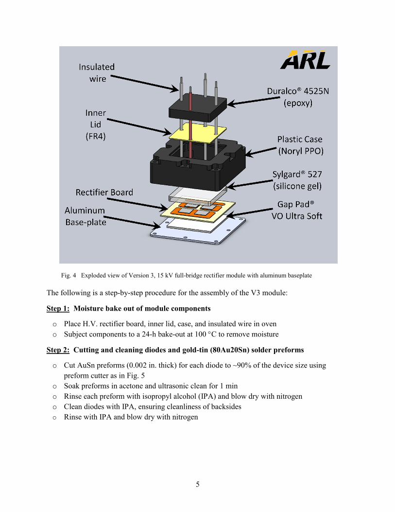
5
Fig. 4 Exploded view of Version 3, 15 kV full-bridge rectifier module with aluminum baseplate
The following is a step-by-step procedure for the assembly of the V3 module:
Step 1: Moisture bake out of module components
o Place H.V. rectifier board, inner lid, case, and insulated wire in oven o Subject components to a 24-h bake-out at 100 °C to remove moisture
Step 2: Cutting and cleaning diodes and gold-tin (80Au20Sn) solder preforms
o Cut AuSn preforms (0.002 in. thick) for each diode to ~90% of the device size using preform cutter as in Fig. 5
o Soak preforms in acetone and ultrasonic clean for 1 min o Rinse each preform with isopropyl alcohol (IPA) and blow dry with nitrogen o Clean diodes with IPA, ensuring cleanliness of backsides o Rinse with IPA and blow dry with nitrogen

6
Fig. 5 Solder preform cutter designed and 3D printed at ARL
Step 3: Bonding of SiC JBS diodes to H.V. rectifier board in vacuum-pressure furnace
o Use the graphite tooling to assemble all the module components as in Fig. 6 o Place the DBC substrate on the tooling base plate o Place the thin graphite template on top of the DBC o Place the AuSn preforms on the DBC in the windows of the template o Place the JBS diodes on top of the preforms o Place the top portion of the tooling over the tooling base plate o Carefully lower the weights through the holes in the tooling o Place the tooling assembly in the vacuum furnace and run AuSn reflow profile (Tpeak =
310 °C; tAL= 1:10 sec)

7
Fig. 6 Tooling used to assemble module components, including inserts, weight assembly, and weights

8
Step 4: Soldering insulated wires onto the DBC substrate using tin-lead (63Sn37Pb) RMA solder
o Use H.V. rectifier inner lid as a locator guide to solder wire leads onto DBC pads o Solder a 12 in. long red wire to DC positive pad, and 12 in. white wire to the other 3
locations as shown in Fig. 7 o Thoroughly clean all flux residue from the wire, DBC, and devices o Ensure that wire insulation will extend below the top surface of the encapsulant when
added
Fig. 7 Photograph of H.V. rectifier board after die attach and soldering of insulated wires
Step 5: Wire bonding devices to DBC
o Wire bonds were made using Orthodyne® Model 20 Ultrasonic bonder o Aluminum wire (0.25 mm) used for all wire bonds as seen in Fig. 8 o Three wire bonds were placed on each device
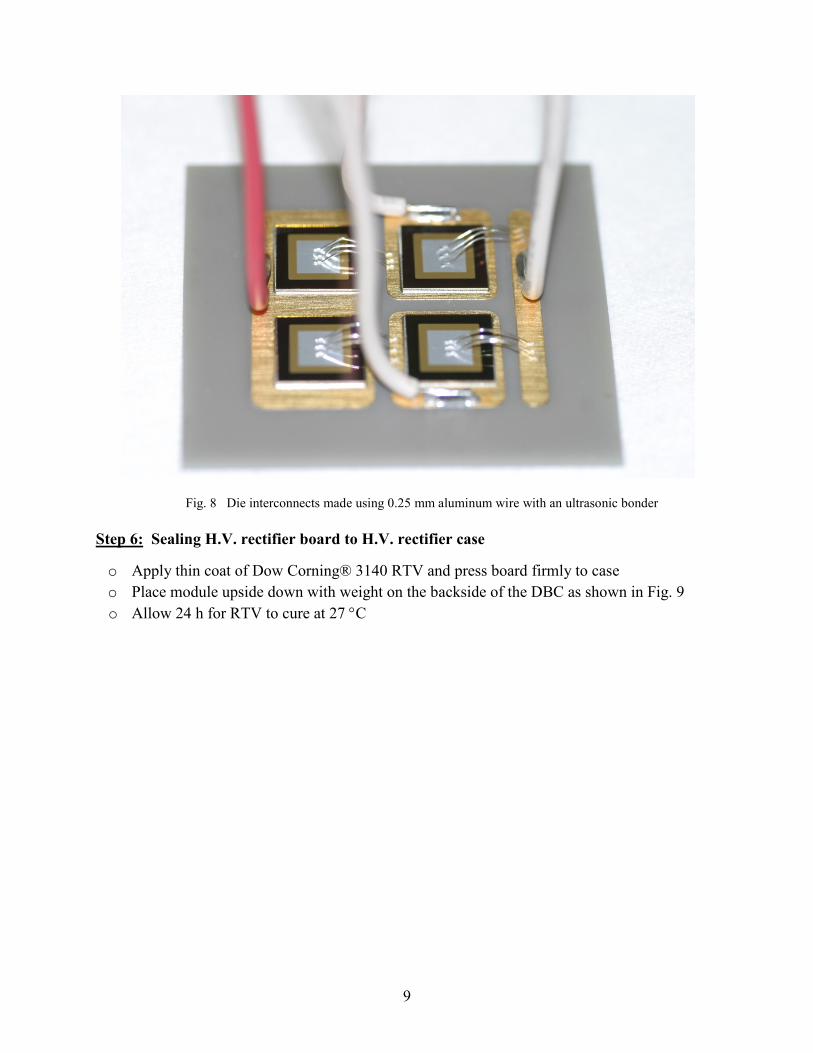
9
Fig. 8 Die interconnects made using 0.25 mm aluminum wire with an ultrasonic bonder
Step 6: Sealing H.V. rectifier board to H.V. rectifier case
o Apply thin coat of Dow Corning® 3140 RTV and press board firmly to case o Place module upside down with weight on the backside of the DBC as shown in Fig. 9 o Allow 24 h for RTV to cure at 27 °C
10
Fig. 9 Photographs depicting process of sealing of H.V. rectifier board to rectifier case using Dow Corning® 3140 RTV coating

11
Step 7: Attach aluminum baseplate to module
o Cut 1.5 mm Bergquist Gap Pad® VO Ultra Soft using template (38 mm × 42 mm) and remove blue film
o Apply the gap pad to the exposed backside of the DBC ensuring that it is centered as in Fig. 10
o Fasten aluminum baseplate to the case using size 4-40 machine screws, nuts, and washers o Securely tighten the screws to compress the gap pad so there is no space between the
aluminum plate and the case

12
Fig. 10 Photographs depicting attachment of aluminum baseplate to module using Bergquist Gap Pad® VO Ultra Soft and size 4-40 machine screws
13
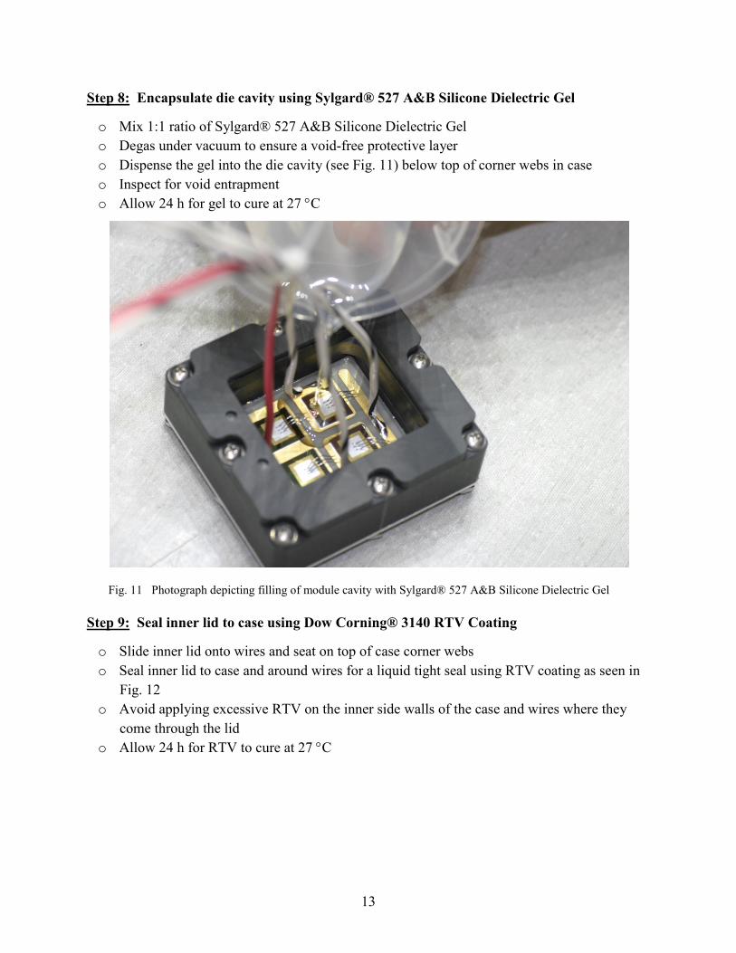
Step 8: Encapsulate die cavity using Sylgard® 527 A&B Silicone Dielectric Gel
o Mix 1:1 ratio of Sylgard® 527 A&B Silicone Dielectric Gel o Degas under vacuum to ensure a void-free protective layer o Dispense the gel into the die cavity (see Fig. 11) below top of corner webs in case o Inspect for void entrapment o Allow 24 h for gel to cure at 27 °C
Fig. 11 Photograph depicting filling of module cavity with Sylgard® 527 A&B Silicone Dielectric Gel
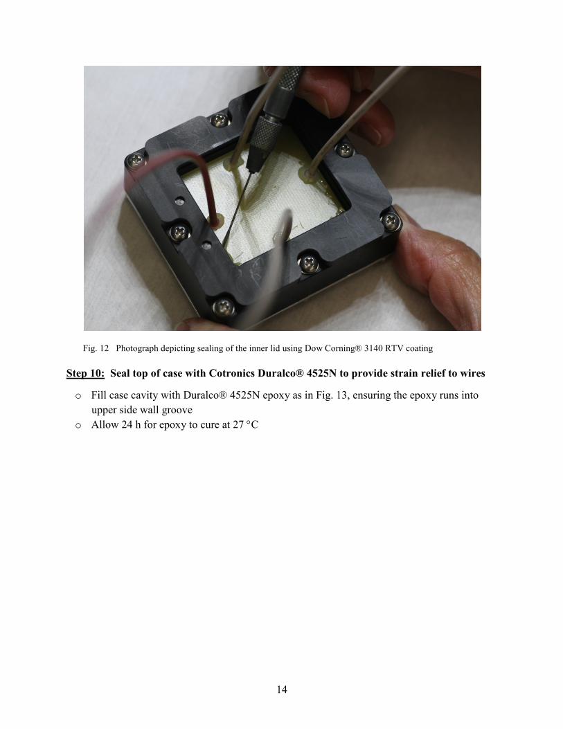
Step 9: Seal inner lid to case using Dow Corning® 3140 RTV Coating
o Slide inner lid onto wires and seat on top of case corner webs o Seal inner lid to case and around wires for a liquid tight seal using RTV coating as seen in
Fig. 12 o Avoid applying excessive RTV on the inner side walls of the case and wires where they
come through the lid o Allow 24 h for RTV to cure at 27 °C
14
Fig. 12 Photograph depicting sealing of the inner lid using Dow Corning® 3140 RTV coating
Step 10: Seal top of case with Cotronics Duralco® 4525N to provide strain relief to wires
o Fill case cavity with Duralco® 4525N epoxy as in Fig. 13, ensuring the epoxy runs into upper side wall groove
o Allow 24 h for epoxy to cure at 27 °C

15
Fig. 13 Photograph depicting fill of case cavity with Cotronics Duralco® 4525N
Table 2 presents properties of the various encapsulants and adhesives used for fabricating the Version 3 module. Figure 14 is a photograph of the completed module.
Table 2 Version 3 module encapsulants & adhesives

16
Fig. 14 Completed Version 3, 15 kV full-bridge rectifier module with aluminum baseplate
5. Conclusions
The advent of SiC devices capable of operating well beyond the voltage regimes of COTS packages has given rise to the need for the development of custom modules for ultra-high voltage operation. Three versions of a high-voltage bridge rectifier module have been developed and fabricated at ARL for pulsed-power applications. Version 2 improved upon Version 1, with the copper baseplate being replaced with a low-CTE CarbAl™ baseplate material, doing away with the issue of crack formation in the ceramic during soldering. The availability of the thicker ceramic layer served to eliminate the requirement of the dielectric pocket for Version 3.
17
List of Symbols, Abbreviations, and Acronyms
AlN aluminum nitride
COTS commercial off-the-shelf
CTE coefficient of thermal expansion
DBC direct bonded copper
ENIG electroless nickel immersion gold
H.V. high voltage
IPA isopropyl alcohol
JBS junction-barrier Schottky
RTV room temperature vulcanization
SiC silicon carbide

18
1 DEFENSE TECHNICAL (PDF) INFORMATION CTR DTIC OCA 2 DIRECTOR (PDFS) US ARMY RESEARCH LAB RDRL CIO LL IMAL HRA MAIL & RECORDS MGMT 1 GOVT PRINTG OFC (PDF) A MALHOTRA 4 DIRECTOR (PDFS) US ARMY RESEARCH LAB RDRL SED P D IBITAYO G KOEBKE D URCIUOLI W TIPTON