Fabrication of Electroluminescent Silicon Diodes by Plasma...
124
Fabrication of Electroluminescent Silicon Diodes by Plasma Ion Implantation A Thesis Submitted to the College of Graduate Studies and Research in Partial Fulfillment of the Requirements for the degree of Master of Science in the Department of Physics and Engineering Physics University of Saskatchewan Saskatoon By Phillip Desautels c Phillip Desautels, December 2009. All rights reserved.
-
Upload
vuonghuong -
Category
Documents
-
view
218 -
download
1
Transcript of Fabrication of Electroluminescent Silicon Diodes by Plasma...

Fabrication of Electroluminescent
Silicon Diodes by Plasma Ion
Implantation
A Thesis Submitted to the
College of Graduate Studies and Research
in Partial Fulfillment of the Requirements
for the degree of Master of Science
in the Department of Physics and Engineering Physics
University of Saskatchewan
Saskatoon
By
Phillip Desautels
c©Phillip Desautels, December 2009. All rights reserved.

Permission to Use
In presenting this thesis in partial fulfilment of the requirements for a Postgrad-
uate degree from the University of Saskatchewan, I agree that the Libraries of this
University may make it freely available for inspection. I further agree that permission
for copying of this thesis in any manner, in whole or in part, for scholarly purposes
may be granted by the professor or professors who supervised my thesis work or, in
their absence, by the Head of the Department or the Dean of the College in which
my thesis work was done. It is understood that any copying or publication or use of
this thesis or parts thereof for financial gain shall not be allowed without my written
permission. It is also understood that due recognition shall be given to me and to the
University of Saskatchewan in any scholarly use which may be made of any material
in my thesis.
Requests for permission to copy or to make other use of material in this thesis in
whole or part should be addressed to:
Head of the Department of Physics and Engineering Physics
116 Science Place
University of Saskatchewan
Saskatoon, Saskatchewan
Canada
S7N 5E2
i

Abstract
This thesis describes the fabrication and testing of electroluminescent diodes
made from silicon subjected to plasma ion implantation. A silicon-compatible, elec-
trically driven light source is desired to increase the speed and efficiency of short-
range data transfer in the communications and computing industries. As it is an
indirect band gap material, ordinary silicon is too inefficient a light source to be
useful for these applications. Past experiments have demonstrated that modifying
the structural properties of the crystal can enhance its luminescence properties, and
that light ion implantation is capable of achieving this effect. This research inves-
tigates the relationship between the ion implantation processing parameters, the
post-implantation annealing temperature, and the observable electroluminescence
from the resulting silicon diodes.
Prior to the creation of electroluminescent devices, much work was done to im-
prove the efficiency and reliability of the fabrication procedure. A numerical algo-
rithm was devised to analyze Langmuir probe data in order to improve estimates of
implanted ion fluence. A new sweeping power supply to drive current to the probe
was designed, built, and tested. A custom software package was developed to im-
prove the speed and reliability of plasma ion implantation experiments, and another
piece of software was made to facilitate the viewing and analysis of spectra measured
from the finished silicon LEDs.
Several dozen silicon diodes were produced from wafers implanted with hydrogen,
helium, and deuterium, using a variety of implanted ion doses and post-implantation
annealing conditions. One additional device was fabricated out of unimplanted,
unannealed silicon. Most devices, including the unimplanted device, were electrolu-
minescent at visible wavelengths to some degree. The intensity and spectrum of light
emission from each device were measured. The results suggest that the observed lu-
minescence originated from the native oxide layer on the surface of the ion-implanted
silicon, but that the intensity of luminescence could be enhanced with a carefully
chosen ion implantation and annealing procedure.
ii

Acknowledgements
I would like to extend my gratitude to my supervisor, Dr. Michael P. Bradley,
for his steadfast support and encouragement throughout the course of this project.
I also wish to thank Dr. Chary Rangacharyulu for useful discussions and comments.
All ion implantation in this work was carried out using a customized Plasmion-
ique ICP600 plasma system, with the high-voltage pulse generator originally designed
by J. T. Steenkamp and later refined and maintained by myself and fellow M. Sc.
students Darren Hunter and John McLeod. The system was funded by a CFI New
Opportunities Fund Grant held by Dr. Michael P. Bradley, titled “Plasma Ion Im-
plantation experiment for new photonic materials.” I am also thankful to Dr. Akira
Hirose for providing the plasma chamber that originally allowed our lab to pursue
this line of research, and to Dr. Chijin Xiao for generously loaning us a spectrometer
for use in this research. Thanks also go to former M. Sc. students J. T. Steenkamp
and Marcel Risch for their development of sheath modelling and fluence prediction
software that improved the quality of this work substantially.
I am indebted to Perry Balon, Ted Toporowski, and Blair Chomyshen at the
Physics Machine Shop for their help in machining various pieces of hardware for my
project, and to David McColl for general technical support and for a generous policy
regarding the use of his tools. I am grateful to Dr. Stephen Urquhart from the Dept.
of Chemistry for volunteering the use of his evaporator for this research, and also to
Mitra Masnadi Khiabani for her assistance with that equipment.
Financial support for this research was provided by the NSERC Postgraduate
Scholarship program and NSERC Discovery Grant 298455-08 (“New methods and
ideas in silicon-compatible photonics”) and supplemented by the Dept. of Physics
and Engineering Physics at the University of Saskatchewan.
iii

Contents
Permission to Use i
Abstract ii
Acknowledgements iii
Contents iv
List of Tables vi
List of Figures vii
List of Abbreviations ix
List of Symbols x
1 Introduction 1
2 Condensed Matter Physics 42.1 Luminescence and Carrier Lifetimes . . . . . . . . . . . . . . . . . . . 5
2.1.1 Shockley-Read-Hall Recombination . . . . . . . . . . . . . . . 62.1.2 Radiative Recombination . . . . . . . . . . . . . . . . . . . . . 72.1.3 Auger Recombination . . . . . . . . . . . . . . . . . . . . . . . 82.1.4 Recombination in Silicon Devices . . . . . . . . . . . . . . . . 9
2.2 Possible EL Mechanisms in Silicon . . . . . . . . . . . . . . . . . . . 112.2.1 Quantum Confinement Effects . . . . . . . . . . . . . . . . . . 112.2.2 Hydrogenated Silicon . . . . . . . . . . . . . . . . . . . . . . . 142.2.3 Luminescence from Oxides . . . . . . . . . . . . . . . . . . . . 15
2.3 Preliminary Experiments . . . . . . . . . . . . . . . . . . . . . . . . . 17
3 Plasma Ion Implantation 213.1 Plasma Overview . . . . . . . . . . . . . . . . . . . . . . . . . . . . . 233.2 Plasma Sheaths . . . . . . . . . . . . . . . . . . . . . . . . . . . . . . 25
3.2.1 Matrix Sheath . . . . . . . . . . . . . . . . . . . . . . . . . . . 263.2.2 Child-Langmuir Sheath . . . . . . . . . . . . . . . . . . . . . . 273.2.3 Pre-Sheath Region . . . . . . . . . . . . . . . . . . . . . . . . 37
3.3 Langmuir Probe Analysis . . . . . . . . . . . . . . . . . . . . . . . . . 373.3.1 Plasma Potential . . . . . . . . . . . . . . . . . . . . . . . . . 393.3.2 Electron Temperature . . . . . . . . . . . . . . . . . . . . . . 393.3.3 Plasma Density . . . . . . . . . . . . . . . . . . . . . . . . . . 40
3.4 Fluence Prediction . . . . . . . . . . . . . . . . . . . . . . . . . . . . 403.5 Depth and Damage Profiles . . . . . . . . . . . . . . . . . . . . . . . 42
iv

4 Device Fabrication 444.1 Silicon Wafers . . . . . . . . . . . . . . . . . . . . . . . . . . . . . . . 454.2 Vacuum System . . . . . . . . . . . . . . . . . . . . . . . . . . . . . . 454.3 Plasma Source . . . . . . . . . . . . . . . . . . . . . . . . . . . . . . . 484.4 Langmuir Probe . . . . . . . . . . . . . . . . . . . . . . . . . . . . . . 494.5 Solid State Marx Generator . . . . . . . . . . . . . . . . . . . . . . . 52
4.5.1 Digital Signal Pulse Generator . . . . . . . . . . . . . . . . . . 524.5.2 Sample Holder . . . . . . . . . . . . . . . . . . . . . . . . . . 54
4.6 QtPlasmaConsole Software . . . . . . . . . . . . . . . . . . . . . . . . 564.7 Annealing Furnace . . . . . . . . . . . . . . . . . . . . . . . . . . . . 574.8 Metal Evaporator . . . . . . . . . . . . . . . . . . . . . . . . . . . . . 604.9 Apparatus for Spectrometry . . . . . . . . . . . . . . . . . . . . . . . 60
4.9.1 Calibration for Quantum Efficiency . . . . . . . . . . . . . . . 614.9.2 SpectralAnalyzer Software . . . . . . . . . . . . . . . . . . . . 63
5 Results 675.1 Depth and Damage Profiles . . . . . . . . . . . . . . . . . . . . . . . 705.2 Electrical Properties . . . . . . . . . . . . . . . . . . . . . . . . . . . 705.3 Sources of Uncertainty . . . . . . . . . . . . . . . . . . . . . . . . . . 725.4 Luminescence from Unimplanted Silicon . . . . . . . . . . . . . . . . 745.5 Luminescence from Ion Implanted Devices . . . . . . . . . . . . . . . 76
5.5.1 Hydrogenation of Helium-Implanted Devices . . . . . . . . . . 765.5.2 Deuterium Implantation and Lattice Damage . . . . . . . . . 775.5.3 Efficiency over Time . . . . . . . . . . . . . . . . . . . . . . . 805.5.4 Efficiency and Current Density . . . . . . . . . . . . . . . . . 805.5.5 Spectroscopic Measurements . . . . . . . . . . . . . . . . . . . 80
5.6 Discussion of Results . . . . . . . . . . . . . . . . . . . . . . . . . . . 84
6 Conclusion 926.1 Fabricated Devices . . . . . . . . . . . . . . . . . . . . . . . . . . . . 936.2 Potential Applications . . . . . . . . . . . . . . . . . . . . . . . . . . 946.3 Future Work . . . . . . . . . . . . . . . . . . . . . . . . . . . . . . . . 95
References 96
A Quantum Efficiency Calculation 103A.1 Geometric Factor . . . . . . . . . . . . . . . . . . . . . . . . . . . . . 103A.2 Detector Efficiency . . . . . . . . . . . . . . . . . . . . . . . . . . . . 104
B Custom Devices and Tools 107B.1 Digital Pulse Generator . . . . . . . . . . . . . . . . . . . . . . . . . 107B.2 Langmuir Probe Power Supply . . . . . . . . . . . . . . . . . . . . . . 108B.3 Software Screenshots . . . . . . . . . . . . . . . . . . . . . . . . . . . 108
v

List of Tables
2.1 Plasma parameters for preliminary hydrogen-implanted devices . . . . 18
3.1 Mean free paths of various ion species . . . . . . . . . . . . . . . . . . 29
4.1 Device fabrication procedure . . . . . . . . . . . . . . . . . . . . . . . 444.2 Relative ion species populations . . . . . . . . . . . . . . . . . . . . . 504.3 QtPlasmaConsole algorithm for PII analysis . . . . . . . . . . . . . . 584.4 SpectraPro 300i and PI-MAX operating parameters . . . . . . . . . . 61
5.1 List of hydrogen-implanted silicon devices . . . . . . . . . . . . . . . 685.2 List of deuterium-implanted silicon devices . . . . . . . . . . . . . . . 685.3 List of helium-implanted silicon devices . . . . . . . . . . . . . . . . . 695.4 Decay in EL efficiency over time . . . . . . . . . . . . . . . . . . . . . 81
vi

List of Figures
2.1 Electronic band structure of crystalline silicon . . . . . . . . . . . . . 42.2 Recombination of charge carriers in silicon . . . . . . . . . . . . . . . 62.3 Internal quantum efficiency in ordinary silicon . . . . . . . . . . . . . 102.4 Energy gaps in confined silicon structures . . . . . . . . . . . . . . . . 122.5 TEM image of hydrogen-implanted silicon . . . . . . . . . . . . . . . 142.6 Luminescence centre model of oxide-based EL . . . . . . . . . . . . . 172.7 EL spectra from preliminary hydrogen-implanted devices . . . . . . . 192.8 Relative EL peak intensities for preliminary H-implanted devices . . . 20
3.1 Schematic overview of plasma ion implantation . . . . . . . . . . . . 223.2 Child-Langmuir sheath structure . . . . . . . . . . . . . . . . . . . . 283.3 Electric potential within a Child-Langmuir sheath . . . . . . . . . . . 283.4 Sheath width for a cylindrical conductor . . . . . . . . . . . . . . . . 363.5 Current-voltage curve measured from a Langmuir probe . . . . . . . . 383.6 Plasma density calculated from Langmuir probe measurements . . . . 41
4.1 Structure of an ion-implanted silicon diode . . . . . . . . . . . . . . . 454.2 PII vacuum system . . . . . . . . . . . . . . . . . . . . . . . . . . . . 464.3 Schematic of the vacuum system . . . . . . . . . . . . . . . . . . . . . 474.4 Measurements of plasma density and temperature . . . . . . . . . . . 504.5 Sweeping voltage for the Langmuir probe . . . . . . . . . . . . . . . . 514.6 Electronics for high-voltage pulsing and the Langmuir probe . . . . . 534.7 Output of a two-stage Marx generator . . . . . . . . . . . . . . . . . 544.8 Effect of surface charging on pulsed high-voltage potential . . . . . . 574.9 Tube furnace . . . . . . . . . . . . . . . . . . . . . . . . . . . . . . . 594.10 Tube furnace heating curve . . . . . . . . . . . . . . . . . . . . . . . 594.11 Spectrometry apparatus . . . . . . . . . . . . . . . . . . . . . . . . . 624.12 PI-MAX image of a broadband spectrum . . . . . . . . . . . . . . . . 664.13 Optical extinction coefficients of gold and silicon . . . . . . . . . . . . 66
5.1 Depth and damage profiles . . . . . . . . . . . . . . . . . . . . . . . . 715.2 Non-ideal diode model . . . . . . . . . . . . . . . . . . . . . . . . . . 735.3 EL efficiency versus diode characteristics . . . . . . . . . . . . . . . . 735.4 Luminescence from the unimplanted silicon device . . . . . . . . . . . 755.5 EL spectrum from the unimplanted silicon device . . . . . . . . . . . 755.6 EL efficiencies from hydrogen-implanted devices . . . . . . . . . . . . 775.7 EL efficiencies from helium-implanted devices . . . . . . . . . . . . . 785.8 EL efficiencies from deuterium-implanted devices . . . . . . . . . . . 795.9 Decay in EL efficiency over time . . . . . . . . . . . . . . . . . . . . . 815.10 EL efficiency as a function of current density . . . . . . . . . . . . . . 825.11 EL Spectra from hydrogen-implanted devices (versus fluence) . . . . . 835.12 EL Spectra from hydrogen-implanted devices (versus anneal) . . . . . 83
vii

5.13 Fitted peak amplitudes from H-implanted devices (versus fluence) . . 855.14 Fitted peak amplitudes from H-implanted devices (versus anneal) . . 855.15 EL spectra from oxide layers, from Heikkila et al. . . . . . . . . . . . 865.16 AFM images of surface blistering, from Wang et al. . . . . . . . . . . 875.17 EL intensity versus annealing temperature, from Kling et al. . . . . . 895.18 Hydrogen content after annealing, from Kling et al. . . . . . . . . . . 91
A.1 Geometry of light measurement . . . . . . . . . . . . . . . . . . . . . 104A.2 Standard CIE luminosity function . . . . . . . . . . . . . . . . . . . . 106A.3 LUMEX SD-LX5093HD spectrum . . . . . . . . . . . . . . . . . . . . 106
B.1 Operational flowchart for the digital pulse generator . . . . . . . . . . 107B.2 Sweeping voltage sawtooth generator . . . . . . . . . . . . . . . . . . 109B.3 Sweeping voltage amplifier . . . . . . . . . . . . . . . . . . . . . . . . 110B.4 Screenshot of the QtPlasmaConsole application . . . . . . . . . . . . 111B.5 Screenshot of the SpectralAnalyzer application . . . . . . . . . . . . . 112
viii
List of Abbreviations
VLSI Very Large Scale IntegrationCMOS Complementary Metal-Oxide-SemiconductorVCSEL Vertical Cavity Surface-Emitting LaserPII Plasma Ion ImplantationICP Inductively Coupled PlasmaEL Electroluminescence, or ElectroluminescentPL Photoluminescence, or PhotoluminescentLED Light-Emitting DiodeSRH Shockley-Read-HallQCLC Quantum Confinement Luminescence CentreTEM Transmission Electron MicroscopyAFM Atomic Force Microscopy
ix

List of Symbols (Chapter 2)
Symbol Meaning Units Notes
~k Crystal momentum vector m−1
E(~k) Electron state energy eV
τ Recombination lifetime s
τSRH Shockley-Read-Hall lifetime
τrad Radiative lifetime
τAuger Auger lifetime
n or p Electron/hole concentration cm−3
ni or pi Intrinsic concentration Constant: 1× 1010 cm−3
n0 or p0 Equilibrium concentration n0p0 = n2i
∆n Excess carrier concentration ∆n = ∆p for elec. inject.
R Bulk recombination rate cm−3s−1 R = ∆n/τ
η Quantum efficiency none
ηi Internal quantum efficiency
ηx External quantum efficiency ηx < ηi
x

List of Symbols (Chapter 3)
Symbol Meaning Units Notes
m Particle mass kg
mi Ion mass Average over ion species
me Electron mass 9.11× 10⁻³¹ kg
v Particle velocity m/s
vi Ion velocity
ve Electron velocity
n Particle density cm−3
ni Ion density
ne Electron density
n0 Bulk plasma density ni,0 = ne,0 = n0
nn Neutral gas density
λDe Plasma Debye length metres
Te Electron temperature eV Boltzmann const. included
I Electric current amperes
Ii Ion current
Ie Electron current
V Electric potential volts
Vp Plasma potential Measured in situ
Vs Sheath edge potential Analytically determined
V0 Conductor potential Chosen by experimenter
r Co-ord. norm. to conductor metres
rs Sheath boundary position
r0 Conductor surface position
A Collecting surface area m2
Ap Probe surface area
As Sheath surface area As > Ap
xi

Chapter 1
Introduction
As the computational speed of microprocessors increases, more attention has been
paid to signal propagation delay in the metal wires linking chips and components
together. Although the speed of an electrical signal on a metal wire is, in principle,
the speed of light (3×10⁸ m/s), in reality it is limited by the electrical characteristics
of the wires themselves: the inductance (L) and capacitance (C) per unit length of
wire impose delays on signal propagation related to the finite time required to store
energy in the wire’s magnetic and electric fields, respectively. As processors are
made faster and their components are made smaller and more closely packed, signal
propagation in the connecting wires tends to be made slower, to the point where
the delay between transmission and reception of information can exceed the time
available for the processor to complete a single cycle. Connections between chips
and between distant components on the same chip are the most problematic, since
the lengths of these connections do not scale down as component density is increased.
Consequently, there is a communications bottleneck in modern computing: while bit
transfer rates between closely spaced on-chip components may become arbitrarily
fast because of the short distances involved, the intermediate connections between
components within a single computer slow the flow of data substantially [1, 2].
The most promising solution to this dilemma is to replace the troublesome metal
wires with optical waveguides or fibres, as has already been done for long-distance
communication with fibre-optic cable. Since the speed of an optical signals depends
only on the refractive index of the material used to make it, rather than on process-
dependent electrical characteristics, optical connections may provide a solution to the
problem of increasing propagation delay in Very Large-Scale Integration (VLSI) sili-
1

con chips. Optical transmission is also free from cross-talk and other electromagnetic
interference that can degrade the performance of electrical systems. Furthermore,
optical pathways lack the Ohmic (I2R) power loss that is present in wired connec-
tions; since power dissipation density has lately become a leading-order engineering
issue in VLSI design, this is yet another advantage to using optical transmission.
Many of the components required for integrated silicon optoelectronics, such
as silicon-based or silicon-compatible waveguides [3], modulators [4], and photode-
tectors [5, 6], have already been developed for use with integrated optoelectronics.
However, because silicon is an inefficient light emitter, most optical interconnec-
tion schemes currently under development rely on existing VCSEL (vertical cavity
surface-emitting laser) units that are made of III-V semiconductors such as GaAs,
due to their superior light emission efficiency. Because these materials are not com-
patible with the crystal structure of silicon, the VCSEL units must be made sep-
arately and bonded to the chip’s substrate at great expense [7]. For practical as
well as economic reasons, a more elegant and cost-effective way of making chip- or
board-level optical connections is desired.
The ideal solution to the problem would be to create electroluminescent (EL)
silicon that could be integrated seamlessly into existing CMOS (complementary
metal-oxide-semiconductor) technology. Unfortunately, the electronic structure of
crystalline silicon makes it a very weak light emitter compared to GaAs and other
III-V semiconductors. Despite this obstacle, the potential utility of luminescent
silicon devices has driven considerable effort toward inducing useful EL from silicon-
based materials. To date, appreciable EL at various wavelengths has been reported
from chemically etched porous silicon [8], silicon nanoparticles embedded in a silicon
dioxide matrix [9], erbium-doped silicon [10], and ion-implanted silicon [11]. These
processes improve EL efficiency in silicon by modifying its electronic properties di-
rectly (as in porous Si and nanocrystals) or by introducing more efficient radiative
mechanisms into a silicon matrix (as in Er doping). The purpose of the present work
is to investigate the applicability of plasma ion implantation (PII) to the production
of useful electroluminescent silicon devices, with a focus on EL mechanisms that do
2

not involve bonding or doping the silicon with rare elements.
Plasma ion implantation is an extremely useful tool in many materials processing
applications, as it allows large quantities of material to be processed over short times
and at low cost. Past work has already demonstrated that silicon implanted with high
doses of hydrogen can become electroluminescent under certain processing conditions
[12, 13], and preliminary work in our own laboratory has confirmed this [14, 15].
However, there are several parameters that may contribute to the emergence of the
observed EL: implant energy, implanted dose, ion mass and chemical properties, post-
implant annealing conditions, the forming of oxides on or within the silicon, and the
types of metal contacts used to form the EL devices themselves. Consequently, there
are several theories regarding the origin of EL in plasma-implanted silicon, and no
consensus has yet been reached.
The remainder of this document will discuss the preparation, execution, and
results of an attempt to create electroluminescent silicon using ion implantation with
hydrogen, helium, and deuterium. Chapter 2 will explain the mechanism behind
luminescence in most semiconductors, explain why ordinary silicon is a poor light
emitter, and describe some of the light emission mechanisms that have been proposed
to explain enhanced EL in silicon devices. Chapter 3 will provide an overview of
plasma ion implantation and its role in the present research. Chapter 4 will describe
the equipment and procedure used to prepare and characterize the implanted silicon
devices. Chapter 5 will discuss and analyze the results of the experiment, and finally
Chapter 6 will present the conclusions drawn from this work and some ideas for
future experiments in this field.
3

Chapter 2
Condensed Matter Physics
In order to effectively study electroluminescence in silicon, it is important to
understand the reason why an ordinary silicon crystal is an inefficient light emitter.
The answer is found in the electronic band structure of the silicon crystal, shown in
Figure 2.1.
Figure 2.1: The band structure of crystalline silicon, from Chelikowsky andCohen [16]. Labels on the horizontal axis represent points and paths within thereciprocal lattice of the Silicon-I crystal (diamond structure), which is shownto the right [17]. The Fermi energy is at 0 eV on the vertical axis.
The band structure represents the dispersion relation E(~k) of several electron
orbitals inside the crystal lattice, where E is the energy and ~k is the crystal momen-
tum of the electron, respectively. These and other symbols used in this chapter are
defined in the List of Symbols on page x. It can be computed (as in Figure 2.1) by
4

modeling the interaction between wavelike electrons and a potential energy function
that depends on the composition and structure of the crystal. The electron wave-
functions used in such a calculation are typically Bloch waves: free electron waves
modulated by periodic functions uk(~r) such that the full electron wavefunctions ψk(~r)
are
ψk(~r) = uk(~r) exp(i~k · ~r
), (2.1)
where uk(~r) is periodic over the same length interval L as the crystal lattice. Given
the complexity of the many-body problem - a periodic arrangement of ion cores and
their electron shells - the true potential within the crystal cannot be determined a
priori. Instead, the ion core potential, including the core electrons (which do not
contribute much to the electronic properties of the crystal) are replaced with an
artificial pseudopotential to allow for converging solutions [16].
2.1 Luminescence and Carrier Lifetimes
From the information presented in Figure 2.1, it is clear that pure silicon is an insula-
tor: the Fermi energy (the maximum energy an electron may have at absolute zero)
lies within a region without any allowed electronic states, called a band gap, which
makes it impossible to drive electric current through the crystal without applying a
very strong electric field and risking damage to the device. However, the band gap
also allows for luminescence if energy can be applied to the electrons in the crystal’s
valence (low energy) band. When electrons are promoted to the conduction (high en-
ergy) band, leaving behind empty states (holes) in the valence band, there are three
principal ways by which the charge carriers may recombine into their original states:
radiative (band-to-band) transitions, which result in photon emission; nonradiative
Shockley-Read-Hall (SRH) recombination at impurity or defect centres, which is cou-
pled to lattice vibrations (phonons); and another nonradiative process called Auger
recombination. These processes are shown schematically in Figure 2.2. The relative
rates at which the three processes occur determine the efficiency of luminescence in
5

Figure 2.2: Schematic representation of the three main recombination pathsfor electron-hole pairs in a silicon crystal. In Shockley-Read-Hall recombination(a), electrons and holes are trapped by defects “d” and recombine nonradia-tively. Radiative (direct, band-to-band) recombination (b) is the direct transi-tion of a conduction electron into a hole in the valence band, which generatesa photon to carry away the released energy. Auger recombination (c) occurswhen the energy and momentum difference between electron and hole states istransferred to another charge carrier instead; the process shown is e-e-h Augerrecombination, but e-h-h recombination is also possible.
the material. Each process is characterized by a mean lifetime τ , which represents
the average time required for an electron-hole pair to recombine via that process.
The following is a brief overview of these recombination processes.
2.1.1 Shockley-Read-Hall Recombination
Shockley-Read-Hall (SRH) recombination occurs when conduction band electrons
recombine with holes via impurities or defects (called recombination centres, or traps)
with energy states deep within the band gap. The energy liberated by this process
is transferred through the impurity or defect to multiple phonons. No photons are
created. SRH recombination is dominant when the defect or impurity concentration
is comparable to the carrier concentration in the material.
Because this recombination channel operates by trapping carriers in a defect
6

state, it does not require that both carriers (electron and hole) be at the same place
at the same time; the defect may trap one carrier for a time, then attract the opposite
carrier at some later time. For this reason, the SRH recombination lifetime does not
strongly depend on the carrier concentration [18]:
τSRH =τp (n0 + n1 + ∆n) + τn (p0 + p1 + ∆n)
p0 + n0 + ∆n, (2.2)
where n0 and p0 represent the equilibrium carrier concentrations, and ∆n is the
excess carrier concentration being injected into the semiconductor. In the case of
an electrically driven semiconductor device, ∆n must equal ∆p to maintain overall
charge neutrality, so the remainder of this discussion will refer only to ∆n. The
coefficients τn and τp represent the trapping lifetimes of electrons and holes (respec-
tively) by the defect or impurity centres, and n1 and p1 are corrections to the carrier
concentrations defined as:
n1 = ni exp
(ET − Ef
T
), p1 = pi exp
(−ET − Ef
T
). (2.3)
The energy ET is the effective energy state of the defect or impurity site and must
lie within the band gap, and the term Ef is the Fermi energy in the semiconductor.
2.1.2 Radiative Recombination
A radiative transition occurs when an electron in the conduction band makes a
direct transition into a hole state in the valence band, releasing the energy difference
between the two states by producing a photon. Such transitions are the means by
which direct band-gap semiconductors such as GaAs produce light. However, the
band gap in silicon is indirect : the maximum energy in the valence band occurs at a
different value of the wavevector ~k than the minimum in the conduction band. Even
though electrons in the crystal are not truly free particles, the quantity ~~k, called
the crystal momentum, must still be conserved in all transitions [19]. Therefore,
the transition between bands requires interaction with phonons to account for the
difference in crystal momentum, which strongly reduces the rate at which these
transitions occur.
7

Unlike the SRH process, radiative recombination does require the simultaneous
presence of two carriers in the same location [20]. Therefore, the radiative recombi-
nation lifetime depends on the carrier density as
τrad =1
B (n0 + p0 + ∆n). (2.4)
As the coefficient B must reflect the likelihood of radiative recombination, one ex-
pects its value in silicon should be lower than its value in a direct-bandgap semicon-
ductor like GaAs. In bulk silicon at 300 K, the coefficient B is 9.5×10⁻¹⁵ cm3s−1 [21],
whereas the value of B in GaAs has been measured to be between 1 and 5× 10⁻¹⁰
cm3s−1, depending on the composition of the compound and the conditions of the
experiment [22,23].
2.1.3 Auger Recombination
Auger recombination occurs when an electron-hole pair donates energy and crystal
momentum to a third charge carrier; this process can involve either two electrons
and one hole or two holes and one electron, with the former process being more
common. No photon is generated. The energized carrier releases its extra energy
to multiple phonons over time, a process called thermalization. Because the Auger
process requires the participation of three carriers at once, the Auger lifetime is
related to carrier density as
τAuger =1
Cp (p20 + 2p0∆n+ ∆n2) + Cn (n2
0 + 2n0∆n+ ∆n2), (2.5)
which has been verified experimentally in silicon for a wide range of dopant concen-
trations [24, 25]. Since electrons may transfer both energy and momentum via the
Auger process, the likelihood of Auger recombination is not strongly dependent on
whether the band gap is direct or indirect.
The Auger coefficients Cn and Cp have been shown to vary with dopant concen-
tration and injection level. For low-injection conditions (∆n << p0) the values of Cn
8

and Cp at 300 K are given by the formula [25]
Cn = Cn,0
[1 + 44
[1− tanh
(n0 + ∆n
5× 1016 cm−3
)0.34]]
, (2.6)
Cp = Cp,0
[1 + 44
[1− tanh
(p0 + ∆n
5× 1016 cm−3
)0.29]]
, (2.7)
where Cn,0 and Cp,0 are the silicon Auger coefficients measured by Dziewior and
Schmid: 2.8 × 10⁻³¹ cm6s−1 and 0.99 × 10⁻³¹ cm6s−1, respectively [24]. In the
high-injection condition (∆n >> p0), the Auger coefficient becomes the so-called
ambipolar coefficient Ca = Cn + Cp and is generally larger than the formulae above
would predict; a typical measured value for Ca is 1.5 × 10⁻³⁰ cm6s−1 for a highly
doped sample. The discrepancy is usually attributed to an enhancement of the Auger
process due to Coulomb interactions [26].
2.1.4 Recombination in Silicon Devices
The overall carrier lifetime τR may be given in terms of the lifetimes from the
Shockley-Read-Hall, radiative, and Auger processes:
τR =
[1
τSRH
+1
τrad
+1
τAuger
]−1
, (2.8)
where the individual terms are defined by Eqs. 2.2, 2.4, and 2.5. One can also define
a bulk recombination rate R as the number of excess-carrier recombinations per cm3
per second; this quantity is related to τ as
R = ∆n/τ, (2.9)
and one finds that in the high-injection limit (∆n >> p0) Eq. 2.8 can be written as
R = KSRH∆n+Krad∆n2 +KAuger∆n3, (2.10)
where the constants K can be derived from the formulae for the lifetimes τ .
It is clear that as the injected carrier concentration ∆n is made large compared
with the dopant and/or defect concentration in the semiconductor, the dominant re-
combination mechanism shifts from the SRH process to the Auger process. The frac-
tion of radiative recombinations reaches a maximum somewhere in between. Since
9

Figure 2.3: An estimate of the internal quantum efficiency in an ordinarysilicon device, as characterized by Eq. 2.11. The silicon is p-type with adopant concentration of 1× 1015 cm−3. A nearly perfect silicon crystal has anSRH lifetime on the order of 1 ms [29]. The SRH recombination lifetime formoderately doped silicon is typically around 1-20 µs [30].
only radiative recombinations generate photons, the internal quantum efficiency ηi
of the material is defined as the fraction of the carriers injected into the crystal that
undergo radiative recombination:
ηi =τRτrad
. (2.11)
The silicon wafers used in the present research are boron-doped (p-type) with
a dopant concentration p0 of approximately 1 × 1015 cm−3, which gives a minority
carrier concentration n0 of 1 × 105 cm−3. Using these values, one can plot the
quantum efficiency as a function of injected carrier concentration ∆n; such a plot is
shown in Figure 2.3. It shows that the maximum possible quantum efficiency of a
silicon device is typically on the order of 10−2, confirming that silicon is an inefficient
light emitter compared to most III-V semiconductors. Internal quantum efficiencies
in excess of 0.8 have been reported for devices made from GaAs [27,28].
Although the derivation of internal quantum efficiency provides insight regarding
10

luminescence in different materials, the quantity itself cannot be measured directly;
ηi does not take into account the possibility of photons being re-absorbed within
the material or otherwise prevented from escaping and being detected in a real
experiment. The number of detectable photons per injected charge carrier in a
semiconductor device is referred to as the external quantum efficiency, ηx, which is
always smaller than ηi and depends in part on the design and fabrication of the
light-emitting device under test. The calculation of ηx for the present experiments
can be found in Appendix A, and measured values of ηx are discussed in Chapter 5.
2.2 Possible EL Mechanisms in Silicon
As Section 2.1 demonstrated, ordinary crystalline silicon at room temperature cannot
be an efficient light emitter. Nevertheless, researchers in the field of silicon photonics
have succeeded in producing photo- and electroluminescent silicon using a variety
of techniques, some of which were briefly listed in Chapter 1. In many cases, and
especially in the case of ion-implanted silicon, the origin of the enhanced luminescence
is not well understood. This section will describe several mechanisms that have
been put forward to explain the phenomenon. A comprehensive discussion of the
theoretical models underlying these hypotheses is beyond the scope of this research;
the discussion here will be limited to the basic physical principles underlying each
mechanism, and references to more thorough treatments of the theory will be given in
each of the relevant subsections. The analysis described in Chapter 5 was conducted
with these mechanisms in mind.
2.2.1 Quantum Confinement Effects
When charge carriers in a silicon crystal are confined in a potential well of very small
dimensions (< 5 nm), their allowed energy states and transitions can be strongly
altered, leading to more efficient luminescence, and at higher photon energies, than
silicon would normally emit. The effect was first observed in photoluminescence
studies of anodically etched porous silicon [31, 32] and has since been confirmed
11

Figure 2.4: Effective energy gaps for various quantum-confined silicon struc-tures. The terms “slab”, “wire”, and “cluster” refer to one, two, and three-dimensional confinement, respectively. The variable d that appears on thehorizontal axis represents the width of the structure in the direction(s) of con-finement. Taken from [35].
by the majority of experimental findings on porous silicon and silicon nanocrystals
[33]. The increase in luminescence intensity through quantum confinement may
be explained by an application of Heisenberg’s uncertainty principle: whereas the
electrons used to calculate the original bandstructure were essentially free, with
well-defined momentum ~~k and uncertain position ~x, a strong localization in ~x-
space forces the electron (and hole) momentum to become uncertain. Consequently,
nearly any phonon in the lattice develops a non-negligible likelihood of facilitating
radiative transitions, instead of only phonons whose ~k-values are equal to that of
the band gap. In cases of extreme confinement, pseudodirect transitions may occur
without the participation of any phonons [33,34].
The increase in radiative energy from quantum-scale silicon structures may be
explained, qualitatively, as follows. As the size of the silicon structure is reduced,
12

the allowed energy states of the system become widely separated; this is somewhat
analogous to the simple particle-in-an-infinite-well problem, although the dependence
of ∆E on d is different. The system can be modeled (using a pseudopotential) as the
interaction between many valence electrons and a matrix of silicon nuclei and core
electron shells. The construction and application of such a model may be found in
the work of Delley and Steigmeier [35], and the results of several groups’ calculations
are shown in Figure 2.4. The data show that the gap energy grows monotonically
with 1/d, and that higher dimensions of confinement tend to produce wider energy
gaps. Therefore, highly confined structures are expected to emit light at shorter
wavelengths. Measurements performed by Wolkin et al. on silicon quantum dots
(three confined dimensions) are in agreement with the data shown in Figure 2.4,
though Wolkin also provides evidence that oxidation of the surface of the silicon
nanocrystals changes their EL spectrum, which he attributes to carrier confinement
at Si=O bond sites [36].
The increased luminescence intensity, coupled with the potential for spectral tun-
ing by controlling the size of the silicon structures, makes quantum confinement very
promising for the development of silicon light sources. Light element plasma ion
implantation and subsequent annealing is known to produce small-scale structures
beneath the surface of implanted silicon; at lower annealing temperatures (250 to
450C) these take the form of nanoblisters that can only be detected through mea-
surement of the lattice displacement field [37], whereas higher-temperature anneals
coarsen the blisters into larger cavities [12, 13] and large surface blisters [38] that
have been observed directly by electron microscopy, as in Figure 2.5. Quantum con-
finement may occur in the thin separations between adjacent cavities, whose size
could be affected by the annealing temperature [37]. Also, the uncontrolled nature
of plasma ion implantation must necessarily produce a wide range of cavity sizes
and separations, which would explain the broad emission spectra exhibited by all
ion-implanted silicon LEDs produced to date.
13
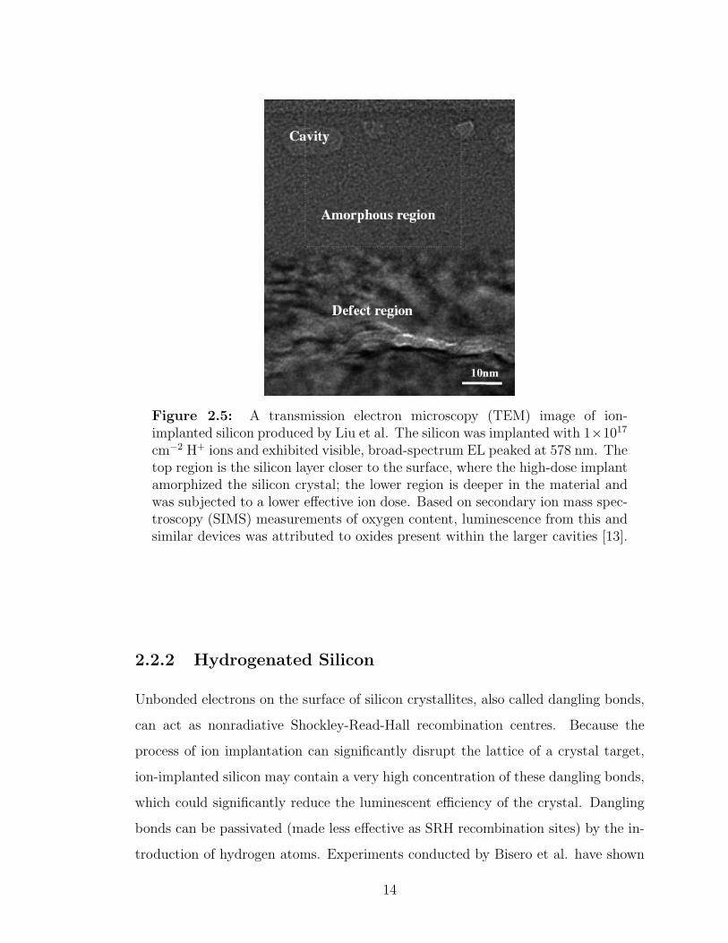
Figure 2.5: A transmission electron microscopy (TEM) image of ion-implanted silicon produced by Liu et al. The silicon was implanted with 1×10¹⁷
cm−2 H+ ions and exhibited visible, broad-spectrum EL peaked at 578 nm. Thetop region is the silicon layer closer to the surface, where the high-dose implantamorphized the silicon crystal; the lower region is deeper in the material andwas subjected to a lower effective ion dose. Based on secondary ion mass spec-troscopy (SIMS) measurements of oxygen content, luminescence from this andsimilar devices was attributed to oxides present within the larger cavities [13].
2.2.2 Hydrogenated Silicon
Unbonded electrons on the surface of silicon crystallites, also called dangling bonds,
can act as nonradiative Shockley-Read-Hall recombination centres. Because the
process of ion implantation can significantly disrupt the lattice of a crystal target,
ion-implanted silicon may contain a very high concentration of these dangling bonds,
which could significantly reduce the luminescent efficiency of the crystal. Dangling
bonds can be passivated (made less effective as SRH recombination sites) by the in-
troduction of hydrogen atoms. Experiments conducted by Bisero et al. have shown
14

that the photoluminescence of silicon implanted with helium ions is strongly depen-
dent on its passivation with hydrogen: samples annealed in a hydrogen atmosphere
exhibited luminescence similar to hydrogen-implanted silicon, a broad peak centred
around 700 nm, whereas samples annealed in vacuum exhibited no luminescence at
all [37]. It should be noted, however, that these observations were made at 77 K,
whereas the devices made and tested in the present research were electroluminescent
at room temperature.
Delerue et al. have presented a two-stage model of capture-recombination at
dangling bond sites. First, an electron or hole is captured by the neutral dangling
bond, which becomes charged; the opposite carrier is subsequently captured by the
charged bond and recombines with the first carrier. According to the model, this
process can be radiative or nonradiative: although it is strongly nonradiative in
bulk silicon, the shift in allowed energy states caused by quantum confinement can
increase the likelihood of photon emission during recombination at dangling bond
sites. The authors suggest that dangling bonds may contribute to luminescence in
the infrared (E < 1.4 eV) and blue-green (E > 2.2 eV) portions of the spectrum,
whereas luminescence between 1.4 eV and 2.2 eV, such as that observed by Bisero et
al., should be suppressed by nonradiative recombination [39]. If this model is correct,
hydrogen passivation of dangling bonds should change the EL spectrum accordingly.
2.2.3 Luminescence from Oxides
Silicon dioxide (SiO2) is naturally present on any silicon surface exposed to air;
this layer of native oxide saturates at a thickness of 0.01 nm at room tempera-
ture [40], but can grow quickly when the silicon is heated. A native oxide thickness
of 1 nm is assumed to exist on all silicon surfaces used in the present research,
in accordance with the measurements of Heikkila et al [41]. SiO2 can itself be a
luminescent material, with visible bands reported at 1.9, 2.2, and 2.7 eV [42, 43].
This has prompted some researchers in the field of silicon photonics to question
whether the observed luminescence from modified-silicon devices might originate
from the oxide layer rather than from the silicon itself. In 1993, Qin and Jia sug-
15

gested that while quantum confinement in nanoscale silicon structures can provide
a well of high energy electron-hole pairs, radiative recombination predominantly oc-
curs at luminescent centres within the oxide layer surrounding the silicon crystal,
not via band-to-band recombinations as was previously believed [44]. The proposed
luminescent centres are primarily composed of silicon-oxygen complexes, but sili-
con hydrides and fluorides were also named as possible contributors. The theory,
called the quantum-confinement-luminescent-centre (QCLC) model, was originally
proposed to explain photoluminescence in porous silicon; specifically, it predicts that
the dominant wavelength emitted by oxidized silicon nanostructures smaller than 8.7
nm should be around 1.8 eV (680 nm) regardless of the structures’ size [45], which
agrees with the findings reported by Wolkin et al. Since the radiative recombination
in this model relies on carrier trapping at luminescence centres, its lifetime τ is not
strongly dependent on the injected carrier concentration.
Although the QCLC model is primarily concerned with photoluminescence from
nanoscale silicon, it can also be used to make a prediction regarding electrolumines-
cence from silicon devices: namely, if the oxide layer is chiefly responsible for silicon
luminescence, then luminescence at roughly the same wavelength should be expected
from any metal-oxide-silicon device, regardless of the presence or absence of nanos-
tructures. Several experiments have produced data in support of this hypothesis:
Qin et al. observed electroluminescence peaked at 690 nm in Au-SiO2-Si structures
that disappeared when the oxide was removed [46], and Heikkila et al. observed
double-peaked EL at 570 and 660 nm in similar devices [41]. Neither experiment ex-
plicitly involved silicon nanostructures of any kind, though Qin et al. suggested that
the oxide layer naturally contained silicon nanoparticles whose energy states were
favourable for activating luminescent centres in SiO2. Based on the QCLC model,
these researchers proposed that radiative recombination in metal-oxide-silicon de-
vices proceeds as shown in Figure 2.6: electrons injected into the metal contact
tunnel into the oxide layer and have some probability of being trapped in defect lev-
els within it. Similarly, holes entering the oxide through the silicon-oxide interface
can become trapped in lower-energy defect states. Carriers that are trapped in this
16

Figure 2.6: The model of oxide-driven electroluminescence in a metal-oxide-silicon device. Panel (a) shows the potential energy levels for electrons and holesfor such a device when no external potentials are applied, whereas (b) showsthe same device when the metal is biased negatively. Electrons injected intothe metal tunnel into the oxide, where there exists a strong electric field; someare trapped in defect states within the oxide, while the remainder continuethrough to the silicon conduction band. Electrons trapped within the oxidecan recombine radiatively with holes that tunnel in from the valence band.After [41].
manner can recombine radiatively within the oxide layer. Although the energy-band-
based explanation of oxide EL does not require the quantum confinement aspect of
the QCLC model, this theory of enhanced silicon EL will still be called the QCLC
model to distinguish it from the purely structural, quantum-confinement-based the-
ory discussed earlier in this Section.
2.3 Preliminary Experiments
Prior to the commencement of the present research, J.T. Steenkamp (a former M.
Sc. student) and James Mantyka (a summer student) prepared a small number of
electroluminescent, hydrogen-implanted silicon devices with a range of ion implant
energies. The device preparation method for these experiments was similar to the
procedure described in Chapter 4, except that the annealing was carried out in a
17

Fisher Scientific muffle furnace under a nitrogen atmosphere. Details of the plasma
processing stage are presented in Table 2.1. The furnace was provided by the under-
graduate laboratory at the Dept. of Chemistry at the University of Saskatchewan;
thanks go to Dr. Pia Wennick for facilitating these experiments. A full account of
the experiment and its results is reported in Ref. [15]. Some of the relevant results
will be presented here to provide context for the present research and to serve as a
point of comparison with the data presented in Chapter 5.
Each device exhibited visible-spectrum luminescence when subjected to an elec-
tric current of 1 A/cm2, driven by an applied potential drop whose value ranged
from 20 to 35 V. The EL spectra measured from the devices are shown in Figure 2.7.
The data have been binned to reduce noise and adjusted to correct for absorption in
the gold electrode; more detail regarding absorption in gold is provided in Section
4.9.2. Each spectrum was also normalized to the same maximum in order to investi-
gate variation in the relative intensities of the peaks as a function of implant energy.
Error bars in the data represent the quadrature sum of random error in the binned
data and the estimated uncertainty in the thickness of the gold electrode.
The data show an apparent shift in the EL spectrum toward longer wavelengths
as the ion implant energy was increased. In contrast, Liu et al., who performed a
similar experiment using hydrogen PII, observed no significant correlation between
EL spectrum and implant energy [13]. To investigate this relationship, the Gaussian
fitting procedure outlined in Section 4.9.2 was performed on each EL spectrum; the
Table 2.1: Plasma parameters for preliminary hydrogen-implanted devices
Parameter Value
Base pressure 1× 10⁻⁶ Torr
Hydrogen gas pressure 1× 10⁻² Torr
Applied RF power 600 W
Electron Temperature 3 eV
Plasma Density 3× 1010 cm−3
Total Fluence (approx.) 2× 1017 cm−2
18

Figure 2.7: Electroluminescence spectra of the preliminary series of hydrogen-implanted silicon devices. Dotted lines represent individual Gaussian functions,the solid line shows the composite fit function, and points represent measureddata. Ion implant energies were 7 keV (a), 15 keV (b), and 18 keV (c).
19

Figure 2.8: The relative intensity of each EL peak from the preliminaryhydrogen-implanted devices as a function of the ion implantation energy. Peaklabels correspond to those used in Figure 2.7.
resulting functions are shown in Figure 2.7, and the relative intensities of the indi-
vidual peaks are plotted in Figure 2.8. The value of the reduced χ2 (a parameter
indicating goodness-of-fit) is conspicuously low for the 7 kV and 15 kV implanted
samples, suggesting that the model may use too many parameters; specifically, peak
IV in the 7 kV implanted sample may not actually exist. Nevertheless, the exper-
iment demonstrated that the ion implant energy can affect the energy distribution
of photons emitted from hydrogen-implanted silicon devices. These results served as
the inspiration for the present research into light-ion-implanted silicon diodes.
20

Chapter 3
Plasma Ion Implantation
Ion implantation is a process in which a target material is bombarded with ener-
getic ions in order to change its properties on or near the surface. Applications for
this technique include: the controlled implantation of impurities into semiconduc-
tors; improving the surface properties of a metal, such as its corrosion resistance or
coefficient of friction; and producing buried layers of altered refractive index within
optical materials to produce high-efficiency waveguides [47]. The main goal of the
present research is to investigate the relationship between the ion implantation pro-
cess and the luminescent properties of ion-implanted silicon diodes.
Two methods exist for performing ion implantation. The first, ion beam implan-
tation, requires ions to be extracted from a remote source, collimated into a beam,
and accelerated toward the target. This presents a number of technical difficulties
and limitations. To limit sputtering, the surface of the target must be normal to the
direction of the beam, so only planar targets may be implanted in this way. The
beam has a limited area, so larger targets must be scanned back and forth, and care
must be taken to ensure an even implant. The ion flux out of the source is also lim-
ited, so implanting a large quantity of ions requires a long time. The chief advantage
of this process is its controllability: ion mass and energy can be precisely selected
while directing the beam, ensuring that only the desired particles are delivered to
the surface [47].
Plasma ion implantation (PII), first developed in the late 1980’s, is an alterna-
tive ion implantation technique that offers many advantages over traditional beam
implantation. In PII, the target is immersed in the ion source (a plasma) and elec-
trically biased to a negative potential by an external energy source. The resulting
21

Figure 3.1: Schematic diagram of the plasma ion implantation process. Anexternal RF source delivers power into a vacuum chamber, which is filled withneutral gas to a pressure of approximately 10 mTorr. This ionizes a small frac-tion of the gas atoms to form a plasma, depicted as an assortment of ions (+)and electrons (-) in the chamber. The silicon target in the center is periodi-cally pulsed to a highly negative potential (VHV ), which propels ions toward,and implants them beneath, its surface. Meanwhile, the plasma density andtemperature are measured using the Langmuir probe as outlined in Section 3.3.The yellow regions surrounding the two conductors represent plasma sheaths,regions of low electron density that will be described in Section 3.2.
22
electric field attracts ions from the plasma and accelerates them toward the target
with energy equal to the applied potential. Because the target is immersed in the
ion source, all incident ions are automatically normal to the target surface, and the
exposed surface of the target receives a uniform ion dose. The dose delivered to the
target is typically much higher than in beam implantation, and can be controlled
by varying the density of the plasma, allowing implants to be completed in much
less time. Furthermore, the apparatus (described by Figure 3.1) is less complex and
can be assembled at a lower cost. The only significant drawback to the PII process
is that the implanted ions cannot easily be selected for either mass or energy: all
ion species are drawn from the plasma simultaneously, and the biasing pulse must
take a finite time to ramp up and ramp down. Nevertheless, PII has found many
applications in the fields of semiconductor processing and metallurgical enhance-
ment [48, 49]. PII has already been used on a limited scale in the field of silicon
photonics, with promising results [12,13,29,37,50,51]. Because the technique allows
for the production of many devices on short timescales and at low cost, PII was the
method used to perform the present research in silicon photonics.
3.1 Plasma Overview
A plasma is a gaseous mixture in which an appreciable fraction of gas particles have
been ionized. The presence of charged particles in the gas makes it responsive to
electric and magnetic fields over large distances, which leads to collective action as
the particles interact with external fields and with each other. Magnetic fields in PII
plasmas are typically very weak, and the analysis presented in this chapter assumes
that magnetic effects are negligible. Because the plasma began as a neutral gas,
there must be equal quantities of positive and negative charge within it; furthermore,
electric forces tend to distribute the charge such that the net charge density, and
therefore the net electric field, is zero throughout the plasma. This property is called
quasineutrality and must hold true in any unperturbed plasma, which will be referred
to as bulk plasma. Perturbations in the plasma, such as charged conductors, create
23

local fields that separate charge and violate quasineutrality in the vicinity of the
perturbation.
In order to perform a quantitative analysis on a PII plasma, one requires knowl-
edge of three properties: the plasma density, the electron temperature, and the plasma
potential. These properties are described below, and can be measured in situ using
a Langmuir probe. The theory behind the Langmuir probe is explained in Section
3.3, while the design and operation of the probe itself are discussed in Section 4.4.
Plasma Density
The plasma density, n0, is the density of electrons within the plasma. Since quasineu-
trality requires that the electron density must equal the positive charge (ion) density,
the densities of all other charged particles may (in principle) be determined from n0.
Electron Temperature
The electron temperature, Te, describes the width of the electrons’ velocity distribu-
tion f(ve), which is typically assumed to be a Maxwellian distribution [52]:
f(ve,j) = n0
(me
2πTe
) 32
exp
(−me |ve|2
2Te
), (3.1)
where |ve| represents the magnitude of the electron’s velocity in three dimensions.
Thus, higher values of Te correspond to higher average electron speeds. By conven-
tion, the electron temperature in processing plasmas is given in units of energy (eV),
with the Boltzmann factor k included within Te.
Plasma Potential
The plasma potential, Vp, is the electric potential of the bulk plasma. In general,
Vp may be set to any convenient value, since electric potential is a relative quantity.
However, in some cases (such as the Langmuir probe analysis in Section 3.3) there
is a body in the system whose potential is referenced to an external ground; in such
situations, Vp becomes an unknown parameter that must be measured.
24

3.2 Plasma Sheaths
Because it is composed of charged particles, a plasma tends to surround any intruding
source of electric fields (such as a charged conductor) with a region of heightened
charge density; this effect restricts the intruding field to a small region immediately
surrounding the source. Nearly all the energy difference between the bulk plasma
potential Vp and the potential of the intruding object V0 is dropped across this region,
which is called a plasma sheath. The strength of the screening effect depends on the
plasma density and temperature: its characteristic length scale, the electron Debye
length, is defined as [52]
λDe =
√ε0Te
n0e2, (3.2)
where all symbols are defined in the List of Symbols on page xi. Depending on the
strength of the intruding electric field, a sheath may be tens or hundreds of Debye
lengths wide, but the physics governing the sheath region are essentially the same in
each case.
Outside the sheath, the plasma is largely unperturbed and the electric field is
nearly zero, as in any bulk plasma. Inside the sheath, quasineutrality is broken,
and the electric field may be very large. All sheaths discussed in this document
are formed around negatively-charged electrodes; that is, the field surrounding the
intruding object tends to push electrons away and draw ions in, creating a sheath
that is ion-rich and electron-poor.
In the steady-state condition, the sheath acts like the space within a plane-parallel
diode, and the ion current follows a relation similar to the Child-Langmuir law for
space charge limited current in such a system. This situation will be discussed at
length in Section 3.2.2. However, if the conductor’s potential V0 is changed very
rapidly, the faster-moving electrons can leave behind a region of uniform ion density
behind as they are pushed away; this creates a short-lived configuration called a
Matrix sheath that will be discussed in Section 3.2.1. Lastly, there must exist a
region between the sheath proper and the bulk plasma, called the transition region
25

or presheath, that may affect the properties of the sheath in subtle ways. These
issues will be briefly discussed in Section 3.2.3.
The behaviour of plasma sheaths is relevant to plasma ion implantation for two
reasons: first, the space charge limited flow of ions through the Child-Langmuir
sheath can be measured with a simple Langmuir probe, and analysis of the rela-
tionship between probe potential and measured current yields information about the
density and temperature of the bulk plasma.
Second, the electric field within the sheath surrounding the silicon target shown
in Figure 3.1 is what accelerates ions toward its surface. Using information obtained
from the Langmuir probe, one can model the behaviour of the sheath region to
predict the number of ions that will be implanted by a given voltage pulse, as well as
the energy distribution of those ions at the point of impact. Past M. Sc. students M.
Risch and J. T. Steenkamp have developed and tested such a model [53,54] based on
the work of M. Lieberman [55], which is employed in the present research to estimate
the number of ions delivered to the silicon targets. An overview of the model will be
presented in Section 3.4.
3.2.1 Matrix Sheath
If the conductor potential V0 is sufficiently large compared with Te, the situation
may arise where the more mobile plasma electrons are ejected from the sheath region
before the slower, more massive ions have time to react to the electric field. Such
a sheath is called a Matrix sheath and is characterized by a uniform ion density
ni,s within the sheath region. The Matrix sheath is not self-consistent, and it must
eventually evolve into a steady-state Child-Langmuir sheath over a timescale tm [56]:
tm ∼=√
2
9
√ε0mi
e2n0
(2V0
Te
) 34
(3.3)
which, for a typical hydrogen PII discharge with pulse voltage V0 of -5 kV, is 740 ns.
Although the Matrix sheath is short-lived, its ion density is very high compared with
that of the Child-Langmuir sheath, and it can contribute a substantial portion of
the total ions implanted by the PII process. The contribution of the Matrix sheath
26

is taken into consideration in the PII fluence prediction model discussed in Section
3.4.
3.2.2 Child-Langmuir Sheath
When the short-lived Matrix sheath decays, the steady-state arrangement that fol-
lows is the space charge limited flow of ions from the plasma (an infinite ion source)
to the grounded or negatively biased conductor (an infinite ion sink). This is called
a Child-Langmuir sheath, and is depicted graphically in Figure 3.2. Due to the sim-
ilarity with a plane-parallel diode, the ion current through the sheath should obey a
relation similar to the Child law for plane-parallel diodes [57],
Ji =4
9ε0
√2e
mi
(V0 − Vs)32
(r0 − rs)2 , (3.4)
where V0, Vs, r0, and rs are all defined for the sheath region by Figure 3.3. One
also expects that a geometric correction to this equation will be necessary if the
object under analysis is not planar. Given Eq. 3.4 as a starting point, one must
find expressions for Vs and rs as well as their precise relationship to the ion current
density Ji in order to carry out a quantitative analysis of the sheath. The presheath
region is somewhat more complex and will be discussed separately in Section 3.2.3.
Simplifying Assumptions
All of the following analysis is based on a few simplifying assumptions:
1. No collisions occur within the sheath.
This means that the mean free path of ions in the sheath λP must be greater
than the width of the sheath, which may be on the order of a hundred Debye lengths
λDe as defined in Eq. 3.2. The mean free path is
λP =1
Nσ, (3.5)
where N is the density of scattering centres and σ is the effective cross-section for the
scattering process in question. In the weakly ionized plasma used for PII, collisions
27

Figure 3.2: A graphical depiction of the steady-state Child-Langmuir sheath.Ions drift into the presheath region from the bulk plasma with near-zero initialvelocity. The weak field within the nearly-quasineutral presheath (see Section3.2.3) accelerates these ions toward the sheath region at rs, where a muchstronger field propels them toward the conductor at r0.
Figure 3.3: Electric potential within the sheath region shown in Figure 3.2.The sheath surrounds a conductor, biased to a potential V0, whose surface liesat r = r0. r is the co-ordinate normal to the surface of the conductor. Thesheath boundary, which separates the sheath region from the presheath andbulk plasma, is shown in blue and marked as (rs, Vs).
28

are dominated by charge-exchange scattering between charged particles and neutrals
[58], so N becomes the neutral density nn. The cross-section for the charge-exchange
interaction σCX is only weakly dependent on ion energy in the energy range of 1-20
keV, and will be assumed to be constant. The values of σCX for the relevant gases
are given in Table 3.1; note that deuterium and hydrogen plasmas are assumed to
share the same value of σCX [59]. The remaining quantities used to calculate the
mean free paths, given a neutral gas pressure of 10 mTorr, are
Te = 3.00 eV,
n0 = 1.00× 10¹⁶ m−3,
N = 3.21× 10²⁰ m−3.
(3.6)
Table 3.1: Mean free paths of various ion species
Neutral Particle Cross Section σCX (m2) Mean Free Path (m) Ref.
H2 4× 10⁻²⁰ 7.8× 10⁻² [60]
D2 4× 10⁻²⁰ 7.8× 10⁻² [60]
He 6× 10⁻²⁰ 5.2× 10⁻² [61]
For the given values of Te and n0, the Debye length λDe is equal to 1.29 × 10⁻⁴
m. Table 3.1 shows that λP > 100λDe for all the listed ion species, so it is reasonable
to assume the sheaths in the present experiments to be collisionless.
2. The electric potential of the bulk plasma is zero.
This is actually a choice, rather than an assumption, since the zero point of
electric potential is arbitrary in most situations. The electric potential of a plasma
within a grounded chamber tends to float positive due to the presence of the electron-
poor Child-Langmuir sheath; if the plasma is used as the zero-point for electric
potential, the potential at the chamber wall must be negative. However, this choice
will not be valid for the analysis of the Langmuir probe in Section 3.3 because the
probe potential must be referenced to the grounded wall rather than to the bulk
plasma.
29

3. The number of electrons absorbed by the conductor is negligible.
The first consequence of this assumption is that the conductor potential must
be negative with respect to the plasma, since a positively-charged conductor would
attract a large electron current. Therefore, given that the bulk plasma is at zero
potential, V (r) < 0 for all positions r within the sheath. Second, the assumption
allows one to find a simple expression for the electron density within the sheath
region. To understand this, consider an electron that enters the sheath, traveling
normal to the conductor surface, with velocity ve,0. At any position r within the
sheath, the electron’s velocity normal to the surface, ve,r, must follow the normal
(Gaussian) distribution
f(r, ve,r) = n0
(me
2πTe
) 12
exp
(eV (r)
Te
)exp
(−mev
2e,r
2Te
), (3.7)
which can be obtained from Eq. 3.1. This distribution should be symmetric at all
points in the sheath. However, the possibility exists that electrons may impact the
conductor and be absorbed by it; when this occurs, some electrons are “missing”
from one tail of the distribution, so Eq. 3.7 becomes a truncated Gaussian. In this
case, the electron density ne within the sheath is
ne(r) =1
2n0 exp
(eV (r)
Te
)[1 + erf
(e(V (r)− V0)
Te
)]. (3.8)
To simplify this expression, one must assume that very few electrons possess enough
energy to reach the conductor; this is the same as asserting erf(
e(V (r)−V0)Te
)∼= 1, or
imposing a condition on the electric potential at the point r:
e (V (r)− V0) Te. (3.9)
Applying this condition to Eq. 3.8, the electron density within the sheath is
ne(r) = n0 exp
(eV (r)
Te
), (3.10)
but only so long as the conductor potential V0 is sufficiently negative, and the posi-
tion r far enough from its surface, to satisfy condition 3.9.
30

4. The ion temperature Ti is zero.
The PII apparatus employs an RF power source to generate an inductively cou-
pled plasma (ICP). The process is designed to energize free electrons and uses
electron-neutral collisions to generate ions. This establishes a gross inequality in
electron and ion temperatures: while the electron temperature Te in an ICP may
be as high as 5 eV, the ion temperature Ti is typically no more than 0.1 eV [62].
Because ions are constantly being lost to the chamber wall and replaced within the
bulk plasma, the average ion thermal energy cannot rise substantially over time, and
thus remains small enough to ignore.
Neglecting the ion temperature allows one to easily determine the ion density in
the sheath region. If the ion thermal velocity is zero, the velocity vi of an ion at
position r within the sheath must be
vi(r) =
√−2eV (r)
mi
, (3.11)
and conservation of ion current Ii (as a function of position) requires that
Ii(r) = A(r)eni(r)vi(r) = constant (3.12)
which defines the ion density, ni(r), as a function of the sheath surface area, A(r). r
is the co-ordinate normal to the surface of the conductor under consideration. The
sheath surface area depends on the shape of the conductor; if the conductor is an
infinite sheet, then A(r) is a constant, whereas for a long cylindrical conductor of
length L, A(r) = 2πrL. This assumption permits one to ignore the more complex
theory of sheath analysis, the orbital-motion-limited (OML) theory [63], on the basis
that all ion motion must be perfectly normal to the conductor’s surface.
Sheath Potential
The next step in the analysis of the Child-Langmuir sheath is the determination
of the electric potential at the sheath boundary, Vs from Figure 3.2. Following the
procedure found in Principles of Plasma Diagnostics [64], one begins by observing
31

from Eqs. 3.11 and 3.12 that
ni(r) = ni(rs)
√V (rs)
V (r), (3.13)
and if quasineutrality is applied at the sheath boundary (ni(rs) = ne(rs)) and Eq.
3.10 is used to evaluate ne, one finds
ni(r) = ne(rs)
√V (rs)
V (r),
= n0 exp
(eV (rs)
Te
)√V (rs)
V (r).
(3.14)
Inserting this result into Poisson’s equation, and using the definition V (rs) = Vs,
returns
∇2V (r) = − e
ε0(ni − ne),
= −en0
ε0exp
(eVs
Te
)[√Vs
V (r)− exp
(eV − eVs
Te
)].
(3.15)
A Taylor expansion of Eq. 3.15 about the sheath boundary (that is, about V (r) = Vs)
returns
∇2V (r) =en0
ε0exp
(eVs
Te
)[1
2Vs
+e
Te
](V (r)− Vs) . (3.16)
Only monotonic solutions to this equation are physical; the potential V (r) does not
oscillate within the sheath region. Keeping in mind that (V (r)− Vs) < 0 within the
sheath region, this imposes an upper bound on the sheath potential Vs:
Vs ≤−Te
2e. (3.17)
To find the lower bound on Vs, one must return to the original expressions for
ion and electron density (Eqs. 3.10 and 3.12), impose quasineutrality, and take the
derivative of the result:
−dVdr
(1
2V (r)+
e
Te
)=
1
A(r)
dA
dr. (3.18)
By inspection, the right side of this equation must be positive for any physical con-
ductor. When the term containing V (r) is zero, the derivative dV/dr must be infinite,
32

which indicates that quasineutrality breaks down at the point where V (r) = −Te/2e.
Given that the region outside the sheath must be quasineutral (by definition), the
point where dV/dr → ∞ must lie within the sheath region. Therefore, the sheath
boundary cannot be closer to the conductor than this point, which imposes a condi-
tion on the sheath potential:
Vs ≥−Te
2e. (3.19)
From the boundary conditions in Eqs. 3.17 and 3.19, then, the value of the sheath
potential Vs must be
Vs =−Te
2e. (3.20)
The value of Vs also determines the speed that ions possess when crossing the
sheath boundary, called the Bohm velocity vB; this is the speed they acquire as they
pass through the presheath from Figure 3.2. If one inserts the result from Eq. 3.20
into the expression for ion velocity (Eq. 3.11), the result is [52]
vB =
√Te
mi
. (3.21)
The fact that the Bohm velocity is substantially greater than the negligible ion
thermal velocity is evidence for the existence of the pre-sheath region between sheath
and bulk plasma; this will be discussed further in Section 3.2.3.
Sheath Boundary Position
Determining the location of the sheath boundary rs is more difficult than finding the
sheath potential Vs. To do so, one must consider Poisson’s equation in the sheath
region, once again making use of Eq. 3.12 for the ion density, and assuming that the
electron density is small enough to neglect. The result is
∇2V = − e
ε0
IiA(r)
√mi
−2eV (r), (3.22)
where Ii, the ion current, does not depend on the distance r from the conductor
surface. However, the change in collecting area A(r) as a function of r may not be
negligible.
33

If the conductor is very large compared with the electron Debye length λDe from
Eq. 3.2, the sheath collecting area becomes a simple constant A, and integration of
Eq. 3.22 over the sheath region yields
rs
λDe
= 1.21
[(−eV0
Te
) 12
− 1√2
] 12[(−eV0
Te
) 12
+√
2
], (3.23)
where V0 is the electric potential at the conductor surface, as always. In the limit
where V0 Vs, Eq. 3.23 reduces to
rs =
√2
3exp
(1
4
)λDe
(eV0
Te
) 34
. (3.24)
This equation is valid for the high-voltage pulses applied to the target in the PII
process and is used in the fluence prediction model discussed in Section 3.4.
In the case where the conductor size is comparable to the electron Debye length,
one cannot assume that A(r) is constant throughout the sheath region. This means
that Eq. 3.22 cannot be solved analytically and a numeric technique must be used
instead to find rs. Such is the case for the Langmuir probe used in the present
experiments: it is a cylinder of radius 0.75 mm, which is of the same order as λDe
and certainly smaller than the sheath width for typical plasma conditions. For a
cylindrical sheath, Eq. 3.22 may be rewritten as
∂2V
∂r2= −1
r
∂V
∂r− 1
r
(e
ε0
Ii2πL
√mi
2e
)(−V )−
12 , (3.25)
where L is the length of the cylindrical conductor.
A simple algorithm for solving first-order differential equations, called the fourth-
order Runge-Kutta method (RK4), is used to compute the value of rs in the cylin-
drical geometry. Before applying RK4 to the problem, Eq. 3.25 must be recast into
a system of first-order differential equations:
d
drV ′ = −1
rV ′ − 1
r
(Ii
2πLε0
√mi
2e
)(−V )−
12 , (3.26)
d
drV = V ′. (3.27)
This system can be solved to find the value of V (r) at all points within the sheath
region. However, the RK4 algorithm requires a complete set of values (r, V (r), V ′(r))
34

for a single point, from which it computes the value of V at all other points. The
only known facts about any particular points in the sheath region are:
V ′(rs) = 0,
V (rs) = −Te
2e,
V (r0) = V0,
where r0 is the radius of the cylindrical conductor, and V0 is the bias applied to the
conductor, as before. This does not constitute a complete set of information about
any point, so the following procedure was developed to find the value of rs:
1. Begin with a starting value (or guess) for the sheath boundary location rs.
2. Solve for V (r) using the RK4 algorithm.
3. Compute the value of V at the point r = r0 for this solution; call this V1.
4. Compare V1 with the true value for the conductor potential, V0.
5. Improve the original estimate rs to find a new estimate r1s using the formula
r1s = r0 + (rs − r0)
√∣∣∣∣V0
V1
∣∣∣∣ (3.28)
6. Repeat until the solution converges to within a predefined tolerance.
Both the RK4 algorithm and the procedure given above have been implemented in
C++, with satisfactory results. Figure 3.4 shows the calculated relationship between
sheath width and ion current for a given electron temperature and conductor poten-
tial. The ion current into a conductor is easily measurable and is proportional to the
plasma density: denser plasmas deliver more ions to the sheath region. Therefore, as
ion current increases, the plasma becomes denser and the sheath becomes narrower.
One expects that the sheath width should converge to the planar-sheath value as the
sheath becomes small compared with the conductor radius, but the data show that
the numerical solution is smaller by a factor of 1.1906 in this limit. The discrepancy
persists even if several non-planar elements are removed from Eq. 3.22. It is also
35
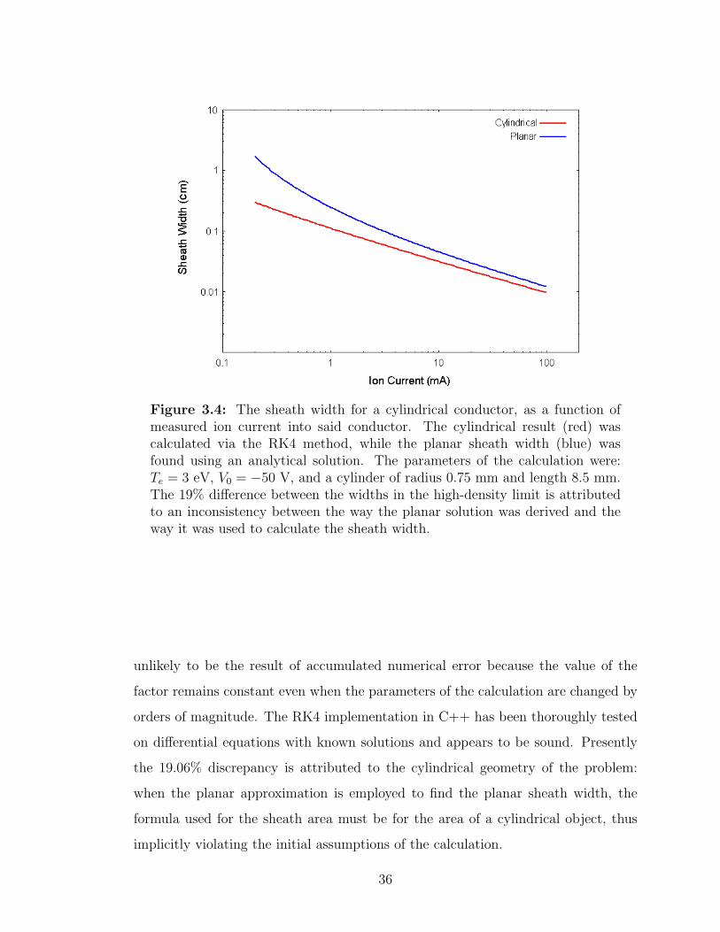
Figure 3.4: The sheath width for a cylindrical conductor, as a function ofmeasured ion current into said conductor. The cylindrical result (red) wascalculated via the RK4 method, while the planar sheath width (blue) wasfound using an analytical solution. The parameters of the calculation were:Te = 3 eV, V0 = −50 V, and a cylinder of radius 0.75 mm and length 8.5 mm.The 19% difference between the widths in the high-density limit is attributedto an inconsistency between the way the planar solution was derived and theway it was used to calculate the sheath width.
unlikely to be the result of accumulated numerical error because the value of the
factor remains constant even when the parameters of the calculation are changed by
orders of magnitude. The RK4 implementation in C++ has been thoroughly tested
on differential equations with known solutions and appears to be sound. Presently
the 19.06% discrepancy is attributed to the cylindrical geometry of the problem:
when the planar approximation is employed to find the planar sheath width, the
formula used for the sheath area must be for the area of a cylindrical object, thus
implicitly violating the initial assumptions of the calculation.
36
3.2.3 Pre-Sheath Region
Since the potential at the sheath boundary Vs is not equal to the potential of the
bulk plasma, one is left with an apparent contradiction: there must be an electric
field in the quasineutral region beyond the sheath. The solution to this problem is
to introduce a presheath region between the sheath and the bulk plasma, in which
a smooth transition between the collision-dominated plasma and the collisionless
sheath may be found. Numerous analytic solutions to the problem have been put
forth: first by Tonks and Langmuir [65], whose work was followed by Lam [66]
and Riemann [67], among others. The properties of the presheath likely have some
influence over the Langmuir probe measurements: for example, it is known that as
the conductor potential V0 becomes more negative with respect to the plasma, the
presheath conditions change so as to enhance the ion current into the conductor [68].
However, these corrections are small compared with the other sources of error in
the measurements, and so the effects of the presheath have been ignored in the
calculations presented here.
3.3 Langmuir Probe Analysis
With the understanding of the Child-Langmuir sheath potential and sheath edge
position from Section 3.2.2, it is possible to probe the plasma with an electric field
in order to determine its temperature and density. The simplest such probe, called
a Langmuir probe, is a small piece of wire that is inserted in the plasma and biased
to a known potential. The wire draws a current from the plasma whose magnitude
and polarity depend on the potential applied to the probe. By sweeping the voltage
over a wide range, one obtains a relation between current and voltage that contains
information about the bulk plasma. This technique, and the analysis that follows,
was developed by Mott-Smith and Langmuir in 1926 [63]. The design of the probe
and the electronics controlling it will be described in Section 4.4. A typical Langmuir
probe curve is shown in Figure 3.5.
37

Figure 3.5: Current-voltage relation produced by the single-electrode Lang-muir probe. The ion saturation region, shown in blue, is where the probepotential V0 is sufficiently negative (relative to the bulk plasma) that a steady-state Child-Langmuir sheath forms around it, and only ions flow into the probesurface. As the potential is made more positive, the electron density in thesheath increases to the point where the electron current becomes larger thanthe ion current; this is called the exponential electron region and is shown inred. The point where the ion and electron current are exactly equal is thefloating potential, Vf .
It should be noted at this point that the potential V0 applied to the probe is
very small compared with the magnitude of the PII implant pulses, and the probe
sweeping frequency is very slow compared to the pulse frequency. This means that
the contribution of the Matrix sheath may be neglected. Also, for the analysis in
this section, zero potential is defined as the potential at the chamber wall, not the
plasma itself (as it was in Section 3.2.2). Therefore, the potential of the plasma
relative to the wall (the plasma potential Vp) is an unknown quantity that must be
measured. Any term V that appears in Section 3.2.2 should be replaced with the
potential difference V − Vp for the following discussion.
38

3.3.1 Plasma Potential
The plasma potential Vp can be found using the floating potential Vf shown in Figure
3.5. Asserting the equality of ion and electron currents (Ii = Ie) at the floating
potential, one finds that [56]
Vf − Vp =Te
2eln
(2πme
mi
), (3.29)
which can easily be solved to find Vp if the value of the electron temperature Te is
known.
3.3.2 Electron Temperature
To determine the electron temperature, one must examine the electron exponential
region, marked in red in Figure 3.5. So long as the difference V0 − Vp is sufficiently
negative with respect to Te/e, the form of the electron density from Eq. 3.10 re-
mains valid. The mean electron speed is taken to be the mean of the Maxwellian
distribution:
ve ≈ vMaxwellian = 2
√2Te
πme
, (3.30)
which gives an expression for the electron current in terms of a collecting area Ae
and the plasma parameters n0 and Te:
Ie = Aeen0
√Te
2πme
exp
(e(V0 − Vp)
Te
). (3.31)
With some manipulation, one finds that in the region between the floating potential
and the plasma potential,
d
dV0
[ln(Itotal − Ii)] =e
Te
, (3.32)
where Itotal is the total current measured in the electron exponential region and Ii
is the current measured in the ion saturation region. Eq. 3.32 can be solved to find
the electron temperature Te without knowledge of Ae or n0.
39

3.3.3 Plasma Density
Given the value of the electron temperature, the plasma density n0 can be extracted
from the measured ion saturation current, marked in blue in Figure 3.5. In this
region, one assumes the electron current to be negligible (Ie = 0). Evaluating Eq.
3.12 at the sheath boundary returns
n0 = − exp
(1
2
)IieAs
√mi
Te
, (3.33)
where As is the area of the sheath boundary and the ion mass mi becomes a weighted
average M in plasmas with multiple ion species according to the formula [69]
√M =
∑j
kj√mi,j, (3.34)
where mi,j is the mass of ion species j and kj is the fraction of the plasma represented
by that species. It is further assumed that all ions crossing the sheath boundary must
ultimately be absorbed by the probe. Depending on the shape and size of the probe,
it may be necessary to use the method described at the end of Section 3.2.2 to find
the sheath collecting area As. The results of such a calculation are shown in Figure
3.6.
3.4 Fluence Prediction
Marcel Risch, a former M. Sc. student working with the PII apparatus, developed a
computer program in ANSI C capable of modeling various aspects of the PII process,
such as the fluence into the target, the ion energy distribution at the target surface,
and the position of the plasma sheath surrounding the implantation target as a
function of time. The program (called p2i) is based on the Lieberman model [55,56]
and is a refinement on earlier work by J. T. Steenkamp [70]. Presented below is a
very brief overview of the model; more details concerning its implementation may
be found in Marcel Risch’s M. Sc. thesis [54].
The Lieberman model assumes that the current into the target is composed of
two parts: the Bohm current due to ions entering the sheath with speed vB, as
40

Figure 3.6: The density of a hydrogen plasma as determined from the mea-sured ion current and computed electron temperature. The cylindrical result(red) was calculated via the RK4 method, while the planar-approximated den-sity (blue) was found using an analytical solution. The density was also calcu-lated assuming a sheath width of zero, for comparison (green). The parametersof the calculation were: Te = 3 eV, V0 = −50 V, and a cylindrical probe ofradius 0.75 mm and length 8.5 mm.
defined by Eq. 3.21; and the motion of the sheath edge rs, which uncovers new ions
as it passes and sends them toward the target. The combined equation is
J = eni(V0, t)
(vB +
d
dtrs(V0, t)
), (3.35)
where V0 is the highly negative pulsed potential being applied to the target. The
model further assumes that the current can be described by the Child-Langmuir law
from Eq. 3.4 at all times; equating the two expressions returns
d
dtrs(V0, t) =
−4
9
ε0eni(V0, t)
√2e
mi
V32
0
rs(V0, t)2. (3.36)
This differential equation is solved using the RK4 method to find the sheath width
as a function of time, which can be inserted back into Eq. 3.4 to calculate the ion
current.
41

3.5 Depth and Damage Profiles
In any ion implantation process, the ions entering the target lose their energy through
collisions with electrons and atomic nuclei in the target. This process leaves a depth
distribution (hereafter called the depth profile) that is roughly Gaussian in nature.
By convention, the mean of the distribution is called the range, and its deviation
is the straggle. These quantities depend on the mass of the implanted ion and the
energy imparted to it by the high-voltage pulse. Heat-activated diffusion during
and after implantation likely changes the profile as well. The depth profile reflects
the amount of material in the target crystal that can be chemically affected by the
implanted element; therefore, if effects such as hydrogen passivation are relevant to
the observed luminescence, one would expect a correlation between the depth profile
and the measured EL.
As the implanted particles pass through the crystal target and collide with atoms
in the lattice, they create a distribution of vacancies and dislocations, hereafter called
the damage profile. One expects that crystals with more vacancies and dislocations
should be more likely to form voids of the type that may cause confinement-related
luminescence; if this is the case, a correlation should be observed between the dam-
age profile and the observed EL. For a detailed treatment of ion-solid interactions,
the reader is directed to the Handbook of Plasma Immersion Ion Implantation and
Deposition [62].
TRIM (Transport of Ions in Matter) is a computer model originally developed
by J. F. Ziegler and J. P. Biersack that simulates the stopping of energetic ions
within crystalline targets. The TRIM model is included in the SRIM (Stopping and
Range of Ions in Matter) package available at www.srim.org. Details of the physical
model used by Ziegler et al. to implement TRIM can be found in Ref. [71]. TRIM
can be used to calculate the depth and damage profiles for hydrogen, helium, and
deuterium implantation into silicon targets. However, TRIM assumes the target is at
absolute zero, so neither diffusion nor self-annealing effects are included in the results.
To account for self-annealing of the crystal during implantation at or near room
42

temperature, the authors of TRIM suggest that the final displacement concentration
should be taken as 1% of the calculated value. One expects that diffusion during
and after implantation should broaden the depth profile considerably, and desorption
from the body of the target is expected to substantially reduce the concentration of
implanted element within the crystal.
43

Chapter 4
Device Fabrication
The method of fabricating electroluminescent silicon diodes used in this work
requires several pieces of equipment: a vacuum chamber with attached gas flow
controllers, an inductively coupled plasma (ICP) generator, a Langmuir probe, a
high-voltage pulse modulator, and an annealing furnace. The light emitted from each
finished device was measured with a spectrometer. This section describes of each
of these items and provides an overview of the whole device fabrication procedure,
as summarized in Table 4.1. A schematic representation of a finished ion implanted
silicon device is shown in Figure 4.1.
Table 4.1: Device fabrication procedure
Procedure Step Equipment Section
1. Load silicon into vacuum chamber Vacuum system 4.2
2. Pump down to base pressure
3. Flow in feedstock gas
4. Initiate the plasma discharge ICP Plasma Source 4.3
5. Measure n0 and Te from plasma Langmuir Probe 4.4
6. Implant ions into silicon Marx generator 4.5
7. Anneal silicon sample(s) Tube furnace 4.7
8. Apply metal contacts Evaporator 4.8
9. Anneal at 400C Tube furnace 4.7
10. Perform spectroscopic analysis Spectrometer 4.9
44

Figure 4.1: The internal structure of a finished ion-implanted silicon diode.There is a thin layer of silicon oxide (SiO2) between the implanted siliconand gold layers that is not shown in this schematic. The thickness of theion-implanted layer depends on the ion mass and implantation energy used.TRIM calculations suggest that a typical penetration depth for 5 keV hydrogenor helium ions is 50 to 100 nm; the final depth profile must also depend onannealing and diffusion effects.
4.1 Silicon Wafers
The silicon wafers used in this research were purchased from NOVA Electronic Ma-
terials, Inc. They are 500 µm thick, boron-doped, p-type, CZ-grown wafers whose
resistivity is in the range of 5 to 25 Ω·cm. The dopant concentration is in the range
of 5 to 20 ×1014 cm−3.
4.2 Vacuum System
Figures 4.2 and 4.3 show the vacuum system used in the present plasma ion im-
plantation experiments. The plasma implantation chamber itself is a cylinder with
an interior volume of approximately 42 L that is connected to two pumps. The
turbomolecular pump, used to pump the chamber down to a base pressure around
1 µTorr, is a 300 L/s Varian TV301 Navigator equipped with water cooling tubes
to maintain optimal working temperature. The mechanical forepump backing the
turbo is an Adixen Pascal 2010 SD series rotary vane pump that works at 2.5 L/s
and can maintain gas pressure as low as 1 mTorr. The mechanical pump is lubricated
45

Figure 4.2: The vacuum system used for the present plasma ion implantationresearch. Frame (a) shows the vacuum chamber itself, along with the Langmuirprobe (LP), thermocouple gauge readout (TCR), and Micro-Ion Plus combi-nation gauge (Ion). Frame (b) shows the underside of the chamber, includingthe vent valve (Vent), mass flow controller (MFC), manual gate valve (Gate),and turbomolecular pump (Turbo, obscured). Frame (c) shows the pump-ing system in the rear of the chamber, including the bypass valve (Bypass),pneumatic valve (V1), thermocouple gauge (TCG), and mechanical roughingpump (Mech). Finally, frame (d) shows the control system for the chamberand pumps (Control), the RF power supply (RF), and the feed gas bottle andregulator (Gas).
46

Figure 4.3: A schematic of the vacuum system shown in Figure 4.2. Thepneumatic valve (V1) and manual gate valve (Gate) are the main evacuationchannel for the two pumps (Turbo, Mech) during normal operation. A thermo-couple (TC) gauge measures the pressure in the foreline, and a cold-cathodeionization (C.C.I.) gauge measures the pressure inside the chamber. The iongauge assembly also incorporates a Pirani gauge and thermocouple gauge inorder to measure a wider range of gas pressures. Feed gases (hydrogen, he-lium, deuterium) are delivered through a computer-controlled pneumatic valve(V2) and the gas flow is regulated by a mass flow controller (MFC). To recom-press the chamber, all valves are closed and the vent valve (Vent) is openedto allow atmosphere back into the chamber. To change samples quickly, theturbomolecular pump may be kept running, isolated under vacuum by closingthe Gate and V1 valves, while the chamber is opened. After the chamber isclosed again, the mechanical pump evacuates the chamber through the bypassvalve (Bypass) before the turbo is reconnected to the system.
47
with inert Fomblin oil (for safety) and equipped with a mist trap and anti-suckback
valve to prevent rapid recompression in the event of power failure. In the standard
pumpdown procedure, the two pumps continuously evacuate the chamber through
the Gate and V1 (pneumatic) valves, and all other valves remain closed.
The flow of feedstock gases (H2, D2, or He) into the chamber is activated by a
pneumatic valve (V2 from Figure 4.3) and the flow rate is regulated by a mass flow
controller. A flow rate of 10 to 15 standard cubic centimetres per minute (sccm)
is typically used. After the gas valve is opened, the gas pressure is controlled by
partially closing the gate valve to reduce the rate at which gas can be pumped out of
the chamber. A Micro-Ion Plus combination gauge (including Pirani, thermocouple,
and cold-cathode ionization gauges) measures the pressure inside the chamber at all
times.
4.3 Plasma Source
Inductively coupled plasma (ICP) sources consist of a conducting coil placed in
close proximity to a gas-filled chamber, with a dielectric (glass or quartz) window
separating the two. Radio-frequency (RF) power applied to the coil induces RF
electric fields within the chamber; these fields accelerate free electrons, and the hot
electrons partially ionize the gas and thereby sustain a plasma discharge [62]. A
dynamic balance is established within the chamber as ions are generated by this
process and lost to collisions with the chamber wall, but an ICP does not reach
thermal equilibrium.
The system used in this work employs a Seren R601 RF power supply operating
at 13.56 MHz that can deliver up to 600 W to the plasma. Its antenna is a flat spiral
conductor positioned above a quartz window that serves as the ceiling of the vacuum
chamber. To maximize the power transfer efficiency from the RF generator to the
plasma, it is connected to a matching network of two variable capacitors whose values
are varied (manually or automatically) until the impedance of the load (plasma plus
capacitors) is as close as possible to the output impedance of the generator. Power
48

transfer efficiencies in excess of 90% can be achieved in this manner.
The plasma density and temperature of an ICP is determined by the combination
of gas pressure within the chamber and RF power delivered to it. Figure 4.4 shows
the relationship between these parameters as measured by the Langmuir probe in a
hydrogen plasma. To save time during the implantation stage, one generally desires
a high-density plasma, so higher values of RF power and gas pressure are preferred.
The only factors limiting these parameters are practical ones: excessive RF power
can overheat the generator if matching is poor or unstable, and given that the gas
pressure is controlled via the manual gate valve, it is difficult to maintain a stable
pressure above 15 mTorr.
Another important parameter in the ICP is the relative population of each ion
species in the plasma. The fluence prediction model discussed in Section 3.4 assumes
that polyatomic ions break apart into their constituent atoms upon impact with the
target surface, and each atom receives an equal fraction of the total kinetic energy.
Therefore, a plasma consisting mostly of H+2 ions will have a shallower depth profile
than one consisting solely of H+ ions. Unfortunately, applicable data regarding
relative populations in hydrogen ICPs are scarce, and an ion-mass spectrometer (not
available for this work) would be required to perform the measurement in situ. The
numbers presented in Table 4.2 are estimates based on measurements of capacitively
coupled [72] and glow discharge [73] plasmas with working pressures on the order of
10 mTorr. No data have been found regarding relative species populations in low
temperature deuterium plasmas, so they were assumed to be identical to the values
for hydrogen. Helium does not form molecules, so it is assumed that only singly
charged monoatomic ions are present in helium plasmas.
4.4 Langmuir Probe
The Langmuir probe used in the present experiments is a simple, single-tip probe
consisting of a tungsten wire sheathed in an alumina tube and surrounded by a
grounded stainless steel shell. The part of the wire exposed to the plasma is a cylin-
49

Figure 4.4: The density and temperature of an inductively coupled hydrogenplasma as a function of (a) applied RF power and (b) neutral gas pressure.Plasma parameters were measured using the Langmuir probe described in Sec-tion 4.4. The gas pressure used while varying RF power was 10 mTorr, andthe RF power applied while varying gas pressure was 400 W.
Table 4.2: Relative ion species populations, after [72, 73]
Plasma Species % of Total Ions
Hydrogen H+ 10
H+2 60
H+3 30
Deuterium D+ 10
D+2 60
D+3 30
Helium He+ 100
50

Figure 4.5: The sweeping voltage generated for the Langmuir probe by customelectronics described in Appendix B, as measured by a Tektronix TD2000Bdigital oscilloscope.
der 8.6 mm long with a radius of 0.75 mm. No provisions are currently in place to
eliminate RF interference from the probe readings, though this does not appear to
significantly degrade the probe’s performance. Tuszewski and Tobin estimate that
the error in calculated plasma parameters from this simple probe setup is approxi-
mately 10% [74].
To perform the analysis described in Section 3.3, electronics capable of generating
a linear voltage sweep over the range of -60V to +30V, and sourcing enough current to
probe the exponential electron region, were designed and built. The circuit was made
manually adjustable to allow the user to compensate for varying plasma parameters,
so the equipment can consistently probe the relevant portion of the current-to-voltage
curve. The instrument can be seen in Figure 4.6, an example of its output is shown
in Figure 4.5, and the electronics are described in more detail in Appendix B.
51

4.5 Solid State Marx Generator
To carry out medium-energy plasma ion implantation, one requires a voltage supply
capable of delivering 5 to 20 kV negative-polarity pulses to the silicon target within
the vacuum chamber. The present work employs a solid-state Marx generator devel-
oped by J.T. Steenkamp for this purpose [70, 75]. A schematic representation of a
two-stage generator is shown in Figure 4.6, and a brief description of how it operates
is presented below.
Each stage of the Marx generator can operate in two modes, called charge and
discharge. In the charge mode, the charging transistors (TCx in Figure 4.6) are
turned on - the collector-emitter paths are conducting - and the discharging transis-
tors (TDx) are off. This causes current from the DC supply to flow in parallel into
the capacitors (Cx) until each one is charged to the full DC potential VDC . When
the two transistors are switched, so TC is off and TD is on, the capacitors become
linked in series to the output terminal Vout; their potentials combine additively to
produce an output voltage equal to
Vout = n · VDC , (4.1)
where n is the number of stages in the Marx generator. Provided that the capacitors
are not allowed to discharge for too long, the output of the device is a nearly flat pulse
with a very small linear droop. To reduce the number of required stages, the output
of the Marx generator is fed into a Westinghouse 610J647H01 pulse transformer. The
transformer steps up the pulse voltage by a factor of ten, though the transformer
slows the pulses’ rise time from 100 ns to approximately 1 µs. Examples of the pulses
produced by this equipment are shown in Figure 4.7.
4.5.1 Digital Signal Pulse Generator
To deliver the correct number of signal pulses to the transistors TCx and TDx in
Figure 4.6, a digital pulse generator was built around a programmable PIC18F4520
microcontroller. The unit includes six buttons and is connected to an LCD unit for
52

Figure 4.6: The custom electronics used to perform the present PII experi-ments. The digital pulse generator (B) drives the gates of the transistors withinthe Marx generator (A) with an optically isolated signal (SIG IN). The Marxgenerator takes power from the custom DC power supply (E to DC-IN) toproduce high-voltage pulses that are sent to the primary coil of the Westing-house 610J647H01 pulse transformer (HV-OUT to F). The secondary coil of thetransformer is connected to the sample holder within the vacuum chamber. Ashunt resistor (G) is placed between the transformer secondary and ground toallow charge on the sample holder to safely dissipate and to dampen parasiticoscillations in the HV pulses. The Langmuir probe electronics (C) are used tomeasure plasma properties prior to implantation. Both Langmuir probe andMarx generator have their output measured by the Tektronix TD2000B digitaloscilloscope (D).
53

Figure 4.7: 20 kV pulses produced by a two-stage Marx generator with aplasma load, as recorded by the Tektronix TD2000B oscilloscope. Graph (a) isthe voltage on the primary (input) coil of the Westinghouse pulse transformer(HV-OUT from Figure 4.6), whereas (b) shows the voltage on the secondarycoil. Taken from [70].
the display of feedback and prompts. The pulse generator allows the user to precisely
control the number, duration, and frequency of high voltage pulses delivered to the
ion implantation target. A flowchart that illustrates the operation of this equipment
is presented in Appendix B.1.
4.5.2 Sample Holder
The output of the Marx generator and pulse transformer is sent through a quartz-
insulated feedthrough to a sample holder within the vacuum chamber. The sample
holder is a circular stainless-steel plate equipped with mounting screws for securing
silicon wafers to its surface. The assembly is equipped with water cooling tubes to
minimize heating during implantation.
54

Sample Heating
During ion implantation, a large flux of energetic ions is bombarding both the silicon
target and the sample holder it is mounted upon; this influx of energy must heat
both target and holder to some degree. The analysis begins with a few assumptions:
1. The thermal conductivity within the target material is high,
2. No heat is lost from the material by radiation or conduction, and
3. Ion kinetic energy is completely converted to heat upon implantation.
These assumptions will give a worst-case estimate of the temperature rise in the
implantation target. The energy Q gained by an object subject to ion bombardment
should be
Q = A · F · U, (4.2)
where A is the area of the target exposed to plasma, F is the total ion flux incident
upon the exposed surface, and U is the average kinetic energy per incident ion. The
specific heat capacity of the material is used to find the change in its temperature:
Q = cmm∆T, (4.3)
where cm is the specific heat capacity per unit mass, m is the mass of material being
implanted, and ∆T is the temperature change in degrees Kelvin. Equating 4.2 and
4.3 produces an expression for the increase in temperature,
∆T =A · F · Ucmm
. (4.4)
For a 4 in. diameter silicon wafer being delivered a flux of 1 × 10¹⁶ ions/cm2 with
an average energy of 5 keV each, the temperature increase ∆T is 96.5 K. This is a
worst-case heating estimate for the implanted silicon wafer; some thermal contact
with the water-cooled sample holder should reduce ∆T . The highest fluence used
in the present research was 2.5× 10¹⁷ ions/cm2, which would result in a worst-case
55

temperature rise of 2412 K. As the melting point for silicon is 1687 K, and the sam-
ples did not melt in the ICP chamber, one must conclude that the cooling apparatus
succeeded in carrying much of the excess heat away from the silicon targets. Un-
fortunately, no equipment is presently in place to measure the actual temperature
reached by the implantation target during the PII process. Regardless, the worst-
case temperature increase for most PII processing was lower than any temperature
used to anneal the finished devices, and so sample heating during implantation is
not expected to be significant except in a small number of extreme cases.
Surface Charging
Marcel Risch investigated the effect of surface charging of the implantation target
on the effective pulse voltage in his M.Sc. thesis, basing his analysis on the work of
Emmert [76]. The main results are reproduced in Figure 4.8. The silicon wafers are
no more than 0.500 mm thick, which means that the potential difference between
the ideal approximation and the actual potential will be no more than 10%. This
result suggests that surface charging effects should be negligible in the present ion
implantation experiments.
4.6 QtPlasmaConsole Software
To facilitate reliable, repeatable ion implantation experiments using the Marx gen-
erator, a program called QtPlasmaConsole was made to incorporate the p2i fluence
prediction code, the Langmuir probe analysis algorithm, and the results of several
TRIM simulations into a single package. The software allows the user to modify
experimental parameters, such as the dimensions of the Langmuir probe or the rela-
tive concentrations of ion species, without manually rewriting the text files used to
store this information. It is coded in C++ and uses the Qt package (available at
qt.nokia.com) to create a user-friendly interface and a plotting window for viewing
results.
The main QtPlasmaConsole interface window is shown in Appendix B.3 as Figure
56

Figure 4.8: The effective electric potential on the surface of a dielectric as afunction of dielectric thickness. The data shown is for a 10 kV implantationpulse and does not account for electrical contact between the dielectric and theconducting sample holder, which would allow excess charge on the dielectric todissipate over time. Taken from [54].
B.4. The application requires two files as input for a calculation: one containing the
voltage and current information retrieved from the Langmuir probe, and another
containing the high-voltage pulse waveform recorded from the Marx generator. The
program executes its analysis of the PII experiment in three stages, shown in Table
4.3.
More information on each of these steps is available in Chapter 3: Section 3.3
explains the analysis of probe data, Section 3.4 describes the fluence prediction
model, and Section 3.5 discusses TRIM simulations.
4.7 Annealing Furnace
After implantation, the silicon samples are thermally annealed in a Barnstead Ther-
molyne 21100 tube furnace, shown in Figure 4.9. To avoid excessive oxide formation
on the surface of the silicon, the tube is attached to a port on the vacuum chamber
57

Table 4.3: QtPlasmaConsole algorithm for PII analysis
Step Inputs Outputs
1. Langmuir probe analysis Probe data Plasma density
Plasma temperature
Plasma potential
2. Ion fluence prediction HV pulse data Implanted ion fluence
Output from (1) Ion energy distribution
3. Depth and damage profiles Energy distribution Depth profile
Output from (1) Vacancy concentration
Saved TRIM results
and the pumping system described in Section 4.2 is used to evacuate the furnace
prior to annealing. The chamber is used for this purpose because the laboratory
lacks a second set of pumps to dedicate to use with the furnace. The pressure in-
side the tube during annealing is typically around 200 µTorr; this is much higher
than ordinary working pressures inside the vacuum chamber due to the length of the
connecting hose and leakage from the tube-hose interface.
Samples are annealed in two stages. After implantation, and prior to metalliza-
tion (described in Section 4.8) the samples are annealed at a temperature chosen
by the researcher that varies from device to device as part of the experiment. The
annealing temperature at this stage is typically between 400C and 800C, and the
time spent at this temperature is about 60 minutes. After the metal contacts are
attached to the silicon (see Section 4.8), a second heat treatment is applied: the
sample is heated to 400C for another 60 minutes to improve the quality of the elec-
trical contact between the silicon and the metals. This second stage will henceforth
be referred to as contact firing. Using higher temperatures during the contact fir-
ing stage ruins the electrical characteristics of the device, and no luminescence was
observed in such cases.
A typical heating curve for the furnace is shown in Figure 4.10. Here, one observes
the main drawback of using this type of furnace: the time required for the furnace
58

Figure 4.9: The Thermolyne 21100 tube furnace used in the present research.The metal hose attached to the left side of the tube connects to the front ofthe vacuum chamber to allow the tube to be evacuated during the annealingprocess.
Figure 4.10: The temperature within the tube furnace as a function of time.The temperature was set to 600C and the pressure within the furnace waspumped down to 1.5×10⁻⁴ Torr before the furnace was activated. The dashedblue line indicates the time when the furnace was turned off.
59

to cool down is very lengthy, which means that the annealing time is not well-
controlled. Removing samples from the furnace during this process was not desirable,
as it would require breaking vacuum and exposing the hot samples to oxygen. More
precise annealing work with better-controlled heating and cooling rates must be left
to future researchers on this project.
4.8 Metal Evaporator
To produce useable electroluminescent devices, metal contacts were attached to each
side of the silicon sample: 150 to 200 nm of aluminum on the unpolished, unim-
planted sides formed Ohmic contacts, and roughly 20 nm of gold was deposited on
the polished, implanted sides to form Schottky junctions. Although the thinness of
the gold layer made the devices very fragile, it was necessary in order to allow light
generated within the implanted silicon to pass outside the device. The transparency
of the gold layer will be addressed in Section 4.9.2.
The metal deposition was accomplished using an evaporator that was made avail-
able by Prof. Stephen Urquhart from the Dept. of Chemistry at the University of
Saskatchewan. The evaporator heats the desired metal to its melting point by driving
a large electric current through the tungsten boat in which the metal was placed; the
vaporized metal deposits itself on the samples, which are suspended directly above
it within an evacuated chamber. The deposition rate and thickness are monitored
by a Sigma Instruments SQM-160 quartz microbalance system.
4.9 Apparatus for Spectrometry
Figure 4.11 shows the spectrometer, camera, and custom sample holder used to
measure light emission from the silicon devices. Power was provided to the devices
by a LAMBDA LG-251 20V regulated power supply, with the gold contact serving
as the anode. Water cooling was necessary during operation because a large current
(in excess of 1.0 A) was required to drive measurable EL in the devices.
60

The spectrometer in Figure 4.11 is a SpectraPro 300i from Acton Research that
was provided by Prof. Chijin Xiao from the Dept. of Physics and Engineering
Physics. The spectrometer is equipped with a 1200 lines/mm grating with a 500 nm
blaze and is connected to a Princeton Instruments PI-MAX intensified CCD camera
for light measurement. Other gratings are also available but were not used in the
present research. Both spectrometer and camera are controlled by computer via the
WinSpec software package. Typical operating parameters for the spectrometer are
listed in Table 4.4.
Table 4.4: SpectraPro 300i and PI-MAX operating parameters
Parameter Typical Value Notes
Grating density 1200 grooves/mm Grating no. 3
Grating blaze 500 nm Grating no. 3
Exposure time 60 s Photometry mode
(typical) 240 s Spectroscopy mode
Camera gain 128 (no units) Recommended by manual
Cosmic ray removal Spatial, 50% Recommended by manual
Dark signal removal None See Section 4.9.2
4.9.1 Calibration for Quantum Efficiency
In addition to performing spectrometry, the spectrometer can operate in a reflective
mode where all light is focused on the camera rather than being dispersed by the
grating. This mode was used to perform photometry on the finished devices. To cal-
ibrate the photometry measurements and obtain a reasonable estimate of the each
device’s external quantum efficiency ηx, the photometry mode was used to measure
the light output of a commercial red LED whose total light output is given in its
datasheet. The number of photons that could be expected to reach the detector was
calculated, and the conversion factor between photons incident on the spectrome-
ter and recorded CCD counts was extracted from that value. Following this, the
61

Figure 4.11: The apparatus used to perform spectrometry on finished electro-luminescent silicon diodes. The Acton Research SpectraPro 300i spectrometer(A) is connected to a PI-MAX camera (B) for light detection. Silicon devicesare loaded into the sample holder (C) and secured beneath a spring-loadedaluminum bar (C1) which serves as the device’s anode. The other bar (C2) issecured to the copper platform and used as the cathode. The wooden frame canbe locked in place during long measurements to ensure stable light transmissioninto the entrance slit of the spectrometer. The entire assembly is water-cooledvia the attached tubes.
62
relationship between the measured intensity from a silicon LED and its external
quantum efficiency was determined. The full calculation is shown in Appendix A;
the final result is
ηx =NCT
β· 2πL2AD
A2slit
· eID, (4.5)
where NCT is the total recorded CCD counts per second from the EL-silicon device,
β is the detector efficiency in counts/photon, L is the distance between the device
and the spectrometer entrance slit, AD is the total surface area of the device, Aslit
is the area of the spectrometer’s entrance slit, and ID is the electric current being
driven through the device. For the present experiments, β is 0.0093 counts/photon,
L is 25 mm, and Aslit is 4 mm2. Inserting these values into Eq. 4.5 returns
ηx = 4.23× 10⁻⁹NCTAD
ID, (4.6)
which gives the external quantum efficiency ηx in terms of the measured EL intensity,
the device area, and the drive current.
4.9.2 SpectralAnalyzer Software
A program called SpectralAnalyzer was designed and implemented to aid in the
plotting and analysis of photometric and spectroscopic data. Its main interface is
shown and described in Appendix B.3. Like QtPlasmaConsole, SpectralAnalyzer is
coded in C++ and uses the Qt utilities to create its graphical components. The
program performs several important functions: it
1. Reads and plots data from WinSpec .SPE format files;
2. Automatically removes the dark current from measured data;
3. Corrects the measured data to account for light absorption in the gold contact;
4. Allows manual plotting and fitting of up to five Gaussian functions;
5. Computes and displays the integrated intensity of the plotted spectrum; and
63

6. Saves the data and the Gaussian fitting parameters in a GNUPLOT-compatible
format.
Use of this program is significantly more efficient than manually manipulating
data with standard software such as Microsoft Excel or MATLAB. The implemen-
tation of several functions is described in more detail below.
Dark Signal Removal
Although WinSpec provides its own background and dark-current removal tools, it
requires that a separate dark spectrum be taken for each recorded image; given that
a full spectrum requires up to 34 images to complete, this is highly time-consuming.
SpectralAnalyzer provides a means of removing such signals post-measurement. Fig-
ure 4.12 shows the image seen by the camera when the spectrometer is illuminated
by a broadband source. The bright zone in the lower two-thirds of the image is
the portion of the camera illuminated by the entrance slit of the spectrometer; the
remainder of the CCD array is cut off from the incident light. To remove the back-
ground signal, SpectralAnalyzer averages the data in this region and subtracts the
result from each point in the illuminated region.
Gold and Silicon Overlayers
Any light emitted from within the silicon itself must pass through the gold conductor,
and possibly through the uppermost layers of silicon, to escape from the device and
be detected by the camera. Neither gold nor silicon has a flat absorption profile
in the visible wavelengths, so the measured spectrum is distorted compared to the
originally emitted light. SpectralAnalyzer compensates for this using the extinction
coefficient for gold measured by Johnson and Christy [77] and an optical model for
silicon developed by Geist [78]. Each model gives values for the extinction coefficient
α of the material, defined as an exponential factor relating the transmitted optical
power PT through a barrier of thickness d to the power incident on the barrier PI ,
64

as in
PT = PI exp (−αd) . (4.7)
The extinction coefficients of gold and silicon are shown in Figure 4.13. Because
the depth of the luminescent centres within the devices are not known, the silicon
absorption profile is not directly applied to the measurements; instead, it is used
to rule out certain possibilities, such as the detection of short-wavelength (blue or
blue-green) emitters from deep within the silicon devices.
Gaussian Fitting
Some analysis of spectral data, notably that found in Section 2.3, was performed by
fitting the spectrum to a multi-Gaussian function to investigate the correlation be-
tween spectral shape and ion implantation parameters. SpectralAnalyzer facilitates
this analysis by plotting up to five Gaussians alongside the corrected spectroscopic
data. It also computes the reduced χ2 value for the fit, defined as
χ2 =1
N − n∑
i
(yi − f(xi))2
σ2i
, (4.8)
where N represents the number of observations (data points), n is the number of
fitted parameters, (xi, yi) is set of recorded data with error bars of magnitude σi for
each point, and f(xi) is the value of the fitted multi-Gaussian function at the point
xi. A χ2 value close to 1.0 represents reasonable agreement with the data, whereas
values greater or less than 1.0 suggest that the model fails to fit some features, or is
fitting noise within the data, respectively. Presently, the SpectralAnalyzer program
does not possess automated curve-fitting algorithms, so it is used to perform a coarse
fitting by trial and error. SpectralAnalyzer saves the results in a format readable to
GNUPLOT, which is used to automate the final fitting analysis using the fit function
native to that software [79].
65

Figure 4.12: An image captured by the PI-MAX camera of a broadbandlight source incident on the spectrometer’s entrance slit. Note that the slitonly illuminates part of the camera’s CCD array; the remainder of the imageis be used for dark current removal.
Figure 4.13: The extinction coefficients of gold and silicon in the visible rangeof wavelengths, in units of nm−1. The thickness of the gold layer is about 20nm for all devices. The thickness of silicon overlayers is not known.
66

Chapter 5
Results
Using the procedure outlined in Chapter 4, 51 ion-implanted silicon diodes were
fabricated under a variety of processing conditions. Roughly half the fabricated
devices were made with hydrogen-implanted silicon, with the remainder split between
helium- and deuterium-implanted devices. The temperature used in the annealing
phase varied from 400C to 800C, and several devices were not annealed at all prior
to the final contact firing at 400C. Implanted ion fluences ranged from 2× 10¹⁵ to
2×10¹⁷ ions/cm2, and the ion implantation energy was 5 keV in each experiment. A
complete list of fabricated devices can be found in Tables 5.1, 5.3, and 5.2. Note that
some devices have “N/A” listed as their annealing temperature, which indicates that
no annealing was performed on those devices prior to contact firing. This notation
will be used for the remainder of this Chapter.
The current-to-voltage relationship of each device was recorded, as well as the to-
tal electroluminescent intensity of the device as a function of forward current density.
Many devices’ EL spectra were also measured. These data were used to investigate
a number of issues raised in Chapter 2 regarding the relationship between ion im-
plantation and silicon electroluminescence. Specifically, this chapter will discuss the
relationships between the observed luminescence and:
1. The number of ions implanted by PII,
2. Lattice damage caused by ion implantation,
3. Annealing conditions, and
4. The presence of hydrogen.
67

Table 5.1: List of hydrogen-implanted silicon devices. Shaded devices wereelectrically unreliable and are not included in the present discussion.
Device Au Contact Anneal Temp Ion Fluence
(nm) (C) (cm−2)
HyA2 21 N/A 2.1× 10¹⁵
HyA3 24 600 2.1× 10¹⁵
HyA4 24 800 2.1× 10¹⁵
HyB2 21 N/A 8.6× 10¹⁵
HyB3 24 600 8.6× 10¹⁵
HyB4 24 800 8.6× 10¹⁵
HyC2 21 N/A 2.0× 10¹⁶
HyC3 24 600 2.0× 10¹⁶
HyC4 24 800 2.0× 10¹⁶
HyD2 21 N/A 4.0× 10¹⁶
HyD3 24 600 4.0× 10¹⁶
HyD4 24 800 4.0× 10¹⁶
Table 5.2: List of deuterium-implanted silicon devices.
Device Au Contact Anneal Temp Ion Fluence
(nm) (C) (cm−2)
DtA1 20 600 1.0× 10¹⁶
DtA2 20 800 1.0× 10¹⁶
DtA3 20 N/A 1.0× 10¹⁶
DtB1 20 600 4.0× 10¹⁶
DtB2 20 800 4.0× 10¹⁶
DtB3 20 N/A 4.0× 10¹⁶
68

Table 5.3: List of helium-implanted silicon devices. Shaded devices wereelectrically unreliable and are not included in the present discussion.
Device Au Contact Anneal Temp Ion Fluence H Implant
(nm) (C) (cm−2)
HeA1 20 600 4.0× 10¹⁶ N
HeA2 20 800 4.0× 10¹⁶ N
HeA3 20 N/A 4.0× 10¹⁶ N
HeB1 20 600 4.0× 10¹⁶ Y
HeB2 20 800 4.0× 10¹⁶ Y
HeB3 20 N/A 4.0× 10¹⁶ Y
HeC1 20 600 2.5× 10¹⁷ N
HeC2 20 800 2.5× 10¹⁷ N
HeC3 20 N/A 2.5× 10¹⁷ N
HeD1 20 600 2.5× 10¹⁷ Y
HeD2 20 800 2.5× 10¹⁷ Y
HeD3 20 N/A 2.5× 10¹⁷ Y
69

5.1 Depth and Damage Profiles
Presented in Figure 5.1 are TRIM calculations of depth and damage profiles for
devices implanted with 4× 10¹⁶ ions/cm2 from H2, D2, and He gases. A 5 kV pulse
was used for each calculation. Device heating, during the annealing and contact firing
stages or the implantation process itself, is expected to broaden the distributions and
promote desorption of gas atoms from the material, but too little is presently known
to make a reliable, quantitative estimate of the effect. There are models of heat-
activated diffusion in semiconductors, such as the SUPREM model developed by the
Integrated Circuits Laboratory at Stanford University [80], but that model applies
only to traditional CMOS dopants such as boron and arsenic and does not include
the light elements used here.
5.2 Electrical Properties
The relationship between the voltage applied to each device and the resulting current
flowing through it (henceforth called the I-V curve) was measured, and the data was
fit to a typical model of a non-ideal diode. The model represents a diode as a series
combination of an ideal diode, a resistor Rd, and a voltage source Vd representing
the diode’s turn-on voltage. The model circuit, along with some sample I-V curves,
are shown in Figure 5.2.
Not all devices exhibited typical diode behaviour. Some were not electrically
stable: when more than 10 V was applied in the forward direction, the current would
jump erratically across a range typically spanning 1 A or more. These devices could
not be characterized using the model described above, and measured light emission
was typically very low and was not repeatable from test to test. Other devices were
highly resistive in nature, sometimes to the point of conducting current equally in
both directions. Devices exhibiting either of these irregularities are marked in red in
Table 5.1 and are excluded from the data presented in this chapter. Contamination of
and/or mechanical damage to the gold contact may be responsible for these problems;
70

Figure 5.1: The (a) depth and (b) damage profiles of hydrogen-, helium-,and deuterium-implanted silicon as calculated by TRIM. All calculations wereperformed assuming an implant energy of 5 keV and ion fluence of 4 × 10¹⁶
cm−2. The magnitudes of both dose and damage profiles scale linearly withimplanted fluence.
71

blemishes and other imperfections in the gold layer were often visible after contact
firing. In particular, the second batch of hydrogen-implanted devices (those labelled
with the numbers 5 through 9 in Table 5.1) were accidentally overheated during
contact firing and proved unreliable upon testing; none of these were used as sources
of data for the present study.
The measured EL efficiency of each reliable device is plotted alongside the devices’
diode characteristics in Figure 5.3. Most devices exhibited a series resistance Rd in
the range of 2 to 8 Ω and a turn-on voltage Vd between 3 and 10 V. The data show
no significant correlation between EL efficiency and either of these parameters.
5.3 Sources of Uncertainty
1. The light emitted from each device was not evenly distributed over the whole
exposed surface area. This may have been caused by imperfections in the gold
contact or by an uneven distribution of the light emitting centres themselves.
Regardless of the cause, the result is that the EL intensity measured by the
spectrometer may not have been equal to the mean intensity emitted by a given
device.
2. The entrance slit of the SpectraPro 300i spectrometer was made 1 mm wide
to increase the signal-to-noise ratio for photometric and spectroscopic mea-
surements. A large slit width causes smearing in the measured EL spectrum,
reducing its resolution. Any spectral features narrower than 5 nm in wave-
length are not expected to be visible in the data.
3. The annealing temperatures listed in Tables 5.1, 5.3, and 5.2 do not include
the contact firing stage, in which all devices were annealed at 400C. There
may also have been heating effects from the PII process (see Section 4.5.2) and
from Ohmic heating during luminescence measurements; device temperatures
at these times were not recorded, so the effect of these sources of heating on
the measured EL cannot be known. However, since the devices did not show
72

Figure 5.2: The I-V curve of the diode model used in the present research(solid line) and measured electrical data from an ion-implanted silicon device(points). The model circuit is shown in the inset. Component values for theplotted data are Rd = 3.04 Ω, Vd = 6.56 V.
Figure 5.3: The measured EL efficiency ηx of each non-defective device versusthe series resistance Rd and turn-on voltage Vd. The forward current in eachdevice during EL measurements was approximately 2.0 A/cm2.
73

visible signs of heat damage after prolonged operation in forward-conducting
mode, it is safe to assume that device temperature did not rise beyond 400C
during EL measurements.
4. The EL efficiency from most devices changed over time while the diode was
conducting current: the unimplanted device X1 became more efficient after sev-
eral hours of operation, whereas most ion-implanted devices lost some fraction
of their EL efficiency under the same conditions. As spectroscopic measure-
ments with the SpectraPro 300i require more than one hour to complete, it
is likely that some devices’ overall efficiency changed over the course of the
measurement, which would distort the measured spectra.
5.4 Luminescence from Unimplanted Silicon
To account for luminescence effects unrelated to implantation, such as the oxide-
based luminescence described in Section 2.2.3, several devices were fabricated out
of unimplanted pieces of the original silicon wafers; unfortunately, only one proved
useable for the present experiments, and time constraints prohibited any additional
fabrication. This device was originally found to be weakly luminescent when sub-
jected to a current density comparable to those used on the ion-implanted devices.
However, the measured EL efficiency was found to increase substantially over time,
and the effect appears irreversible. Light emitted from the unimplanted device after
300 minutes’ exposure to forward current was dimly visible with the naked eye in
dark-adapted conditions. Figure 5.4 reports the measurements of EL efficiency as
a function of forward current and elapsed time. In comparisons with ion-implanted
EL devices, the quoted EL efficiency for the unimplanted device will be the final effi-
ciency, which appeared to have stabilized after 600 minutes of continuous operation.
The device’s EL spectrum was also measured and fitted to a multi-Gaussian
function for comparison with spectra measured from ion-implanted devices; these
results are shown in Figure 5.5. EL from the unimplanted device was predominantly
red-orange, with a single broad peak centred near 650 nm and a smaller, narrower
74

Figure 5.4: The measured EL efficiency of the unimplanted silicon device asa function of forward current density (a) and elapsed time (b). Measurementsin (a) were taken at t = 310 minutes, and the data in (b) were collected whileapplying a current of 2.7 A/cm2 to the device.
Figure 5.5: The EL spectrum measured from the unimplanted silicon device.Dotted lines represent individual Gaussian peaks, the solid line is the compositeGaussian function, and measured data are shown as individual points. Datawere binned prior to Gaussian fitting with a bin size of 50; error boundarieson each point represent the standard deviation of data within each bin and theuncertainty in the thickness of the gold layer.
75

peak at 705 nm. The fact that the unimplanted device was visibly electroluminescent
suggests that the oxide-related luminescence discussed in Section 2.2.3 is a significant
or even dominant contributor to overall device EL. The remainder of this section will
discuss the measurements of ion-implanted devices and identify what, if any, effect
the PII process had on their luminescence properties.
5.5 Luminescence from Ion Implanted Devices
This section examines the photometric measurements of silicon devices implanted
with hydrogen, helium, and deuterium to investigate changes in EL efficiency with
varying ion fluence and annealing temperature. Results from the set of hydrogen-
implanted devices (shown in Figure 5.6) suggest that both parameters influence the
devices’ light output. Peak EL efficiencies measured from devices implanted with
hydrogen fluences of 2.0× 10¹⁶ and 4.0× 1016 cm−2 were considerably greater than
the EL efficiencies measured from lower-fluence devices. Furthermore, the highest
efficiency was found at a different annealing temperature in each case. This suggests
that as the ion fluence is increased, the annealing temperature required to maximize
luminescence also increases. Lastly, annealing at a temperature higher than the
optimal temperature apparently quenches the enhanced luminescence very strongly.
This may be part of the reason why low-fluence devices were inefficient light emitters:
even the contact firing at 400C was too hot to allow for efficient EL.
5.5.1 Hydrogenation of Helium-Implanted Devices
To study the effect of hydrogenation on the EL from ion-implanted silicon devices,
a series of devices were implanted with high fluence of helium ions, and half of these
were subsequently implanted with a low fluence (1 × 1014 cm−2) of hydrogen ions.
These devices are listed in Table 5.3. Photometric measurements from this series of
devices are shown in Figure 5.7. The data clearly demonstrate that hydrogenation
enhances EL efficiency in silicon diodes: the efficiency of each hydrogen-implanted
device was higher than the corresponding helium-only device by a factor ranging
76

Figure 5.6: The EL quantum efficiencies of hydrogen-implanted silicon diodesas a function of implanted fluence and annealing temperature. “N/A” indicatessamples that were not annealed prior to contact firing. The hydrogen fluence foreach device is given in the legend in units of cm−2. The dashed line shows theefficiency of the unimplanted silicon device under similar conditions. Missingbars represent defective devices whose EL characteristics were not recorded.
from 1.5 to 4. The results here also appear to agree with the measurements shown
in Figure 5.6: as with the pure hydrogen-implanted devices, the maximum efficiency
observed from a hydrogen-and-helium-implanted device was found at an annealing
temperature of 600C, although the maximum value (2.28×10⁻⁶) was lower than the
corresponding maximum from the pure-hydrogen series. This may be related to the
lower hydrogen content in the helium-implanted devices, or to the higher vacancy
concentration caused by helium implantation.
5.5.2 Deuterium Implantation and Lattice Damage
To determine whether the observed luminescence was dependent on ion fluence or
on the lattice damage caused by the ion implantation process, several devices were
77

Figure 5.7: The EL quantum efficiencies of helium-implanted silicon diodes asa function of implanted fluence, annealing temperature, and hydrogen content.“N/A” indicates samples that were not annealed prior to contact firing. Thehelium fluence for each device is given in the legend in units of cm−2. Devicesmarked as +H in the legend were also implanted with 1×10¹⁴ H ions/cm2. Thedashed line shows the efficiency of the unimplanted silicon device under similarconditions. Missing bars represent defective devices whose EL characteristicswere not recorded.
implanted with deuterium (listed in Table 5.2), and the results were compared with
the EL observed from hydrogen-implanted devices with similar fluence or damage
characteristics. Figure 5.8a shows one such comparison: the devices represented
there were all implanted with the same ion fluence (4 × 1016 cm−2) but because of
the higher mass of the deuterium ion, the deuterium-implanted samples suffered more
lattice damage during implantation than the hydrogen-implanted devices. According
to TRIM calculations, the peak vacancy concentration just after implantation was
3.7 × 1020 cm−3 in the hydrogen-implanted devices versus 8.5 × 1020 cm−3 in the
deuterium-implanted devices. The data suggest that additional lattice damage, for
78

Figure 5.8: The measured EL quantum efficiencies of deuterium-implantedsilicon diodes as a function of annealing temperature. “N/A” indicates sam-ples that were not annealed prior to contact firing. Graph (a) compares theefficiency of these devices with hydrogen-implanted devices given the same iondose; here, the peak vacancy concentration in the deuterium implants is higherby a factor of 2.3. Graph (b) compares efficiencies between devices subjected toroughly the same lattice damage; here, the peak vacancy concentration in thedeuterium-implanted devices was only 20% higher than that in the hydrogen-implanted devices. Implanted ion fluences for each graph are given in thelegends in units of cm−2. The dashed line shows the efficiency of the unim-planted silicon device under similar conditions. The missing bar represents adefective device whose EL characteristics were not recorded.
the same ion dose, is detrimental to EL efficiency. The deuterium-implanted devices’
EL also exhibits the same trend with respect to annealing temperature as the more
efficient hydrogen-implanted devices; this suggests that the ion dose is the critical
factor in determining the optimal annealing temperature for the devices.
Figure 5.8b shows a different comparison: here, the two sets of devices were
subjected to similar lattice damage by the PII process (a peak vacancy concentration
of 1.8× 1020 cm−3 in the hydrogen-implanted devices versus 2.2× 1020 cm−3 in the
deuterium-implanted devices) but implanted with different doses of their respective
ions. Again, the data suggest that a high ion dose produces enhanced EL and a large
amount of lattice damage has the opposite effect.
79

5.5.3 Efficiency over Time
Unlike the unimplanted device, which was inefficient at first and gradually improved
over time, the EL efficiencies from most ion-implanted devices were found to decay
while the devices were conducting current in the forward direction. Figure 5.9 shows
the EL decay in a device implanted with 2.5 × 10¹⁷ He ions/cm2 and annealed at
800C. The decay appears exponential at first, but becomes roughly linear after
10 minutes of operation. Different devices were found to decay at different rates;
Table 5.4 shows the fraction of EL efficiency lost by several devices over 10 minutes
of continuous operation at 1.3 A/cm2 forward current density. As before, “N/A”
indicates samples that were not annealed prior to contact firing. The early hydrogen-
and helium-implanted devices had already been in use for some time before the decay
was first noted, so no comparable data regarding their decay rates are available.
5.5.4 Efficiency and Current Density
The EL efficiency from each silicon device was found to vary with the applied forward
current density, as shown in Figure 5.10. Several devices exhibited increasing EL
efficiency with increasing current up to a maximum value, after which the efficiency
would fall as the current density was increased further. The effect appears to be
loosely correlated with both ion dose and lattice damage: low-fluence hydrogen-
implanted devices had no local maximum in efficiency in the available range of current
densities, while the high-fluence devices reached their maxima at current densities
between 2.0 and 2.5 A/cm2. The annealing temperature had no apparent effect on
these trends.
5.5.5 Spectroscopic Measurements
In order to better understand the differences between implanted and unimplanted
silicon devices, their EL emission spectra were measured with the SpectraPro 300i
spectrometer. Figure 5.11 compares the EL spectra from hydrogen-implanted devices
annealed at 600C, and Figure 5.12 compares EL spectra from hydrogen-implanted
80

Figure 5.9: The EL efficiency of helium-implanted device HeD2 (see Table5.3) as a function of time. The device was conducting 1.3 A/cm2 of forwardcurrent for the entire period.
Table 5.4: Decay in EL efficiency over time
Device Anneal Temp Ion Fluence Fraction of efficiency
(C) (cm−2) lost after 10 min
HeD2 800 2.5× 10¹⁷ 18%
DtA1 600 1.0× 10¹⁶ 24%
DtA3 N/A 1.0× 10¹⁶ 37%
DtB1 600 4.0× 10¹⁶ 4%
DtB3 N/A 4.0× 10¹⁶ 46%
81

Figure 5.10: The measured EL efficiencies of hydrogen-implanted EL devicesas a function of forward current density. The devices shown here were annealedat 600C.
devices implanted with 4×10¹⁶ ions/cm2. Clearly, each EL emission spectrum shares
several key features: a sharp peak at 705 nm, a shoulder near 670 nm, and a long tail
extending to short wavelengths. The mean wavelength of the shoulder was allowed
to vary from device to device in order to better fit the small variances in shape. The
EL spectrum from the unimplanted device is provided in each graph for comparison.
The data suggest that the dominant EL mechanism was essentially the same
from device to device, possibly with small variations related to the PII process. The
hydrogen-implanted device implanted with a high fluence and annealed at 400C
(labelled HyD2 in Table 5.1) appears to have been particularly affected by the plasma
implantation process, as it is the only device whose spectral shape deviates noticeably
from the others.
To quantify changes in spectral shape, the same Gaussian fitting algorithm de-
82

Figure 5.11: The measured EL spectra from several hydrogen-implanted de-vices, all annealed at 600C. Different curves represent different implanted flu-ences. Spectra have been normalized to the same maximum to simplify thecomparison. The normalized EL spectrum measured from the unimplanteddevice is provided for reference.
Figure 5.12: The measured EL spectra from several hydrogen-implanted de-vices, all implanted with a hydrogen fluence of 4× 1016 cm−2. Different curvesrepresent devices annealed at different temperatures. Spectra have been nor-malized to the same maximum to simplify the comparison. The normalized ELspectrum measured from the unimplanted device is provided for reference.
83

scribed in Section 4.9.2 and applied to the unimplanted device’s spectrum from
Section 5.4 was used on the spectra from Figures 5.11 and 5.12, and the fitted mag-
nitudes of the three dominant Gaussians (at 670 nm, 705 nm, and 750 nm) were
compared with the magnitudes of the corresponding peaks from the unimplanted de-
vice. The results are shown in Figures 5.13 and 5.14. The data suggest that higher
hydrogen fluence enhances EL in the narrow 705 nm peak relative to the other peaks,
that hydrogen implantation with the proper annealing conditions can also enhance
luminescence in the 670 nm shoulder, and that excessively high annealing tempera-
tures tend to quench that same peak. However, the trends are relatively weak, the
number of devices is small, and distortion of the spectra due to EL decay over time
cannot be ruled out, so no firm conclusions can be made based on these observations.
5.6 Discussion of Results
Despite a few significant sources of uncertainty, the data presented here are suf-
ficient to make some reasonably definitive statements regarding the origin of the
observed electroluminescence. Because visible luminescence was observed from the
unimplanted silicon device, it seems clear that the EL was largely or entirely emitted
from the native oxide layer rather than from within the implanted silicon itself. The
high degree of similarity between each measured EL spectrum supports this asser-
tion. The QCLC model of luminescent centres presented in Section 2.2.3 appears
to be a reasonable explanation for these observations. This conclusion is supported
by past experiments with luminescent oxide-on-silicon devices; Figure 5.15 shows
EL spectra recorded from one such experiment, which appear similar to the present
results [41]. Comparable experiments conducted by other researchers in this field
produced similar outcomes [46,81,82].
Although the spectra recorded from the ion-implanted devices were remarkably
consistent, the differences in peak wavelengths and magnitudes from device to de-
vice, and deviations from the spectra shown in Figures 2.7 and 5.15, merit further
discussion. These differences may be explained by the following arguments. First,
84

Figure 5.13: The amplitudes of the three main fitted Gaussians (centredaround 670 nm, 705 nm, and 750 nm) for hydrogen-implanted devices as afunction of implanted hydrogen fluence. All devices shown here were annealedat 600C. Peak amplitudes are scaled by the amplitudes of the correspondingpeaks from the unimplanted silicon device.
Figure 5.14: The amplitudes of the three main fitted Gaussians (centredaround 670 nm, 705 nm, and 750 nm) for hydrogen-implanted devices as afunction of annealing temperature. All devices shown here were implantedwith a hydrogen fluence of 4 × 1016 cm−2. Peak amplitudes are scaled by theamplitudes of the corresponding peaks from the unimplanted silicon device.
85

Figure 5.15: The EL emission spectra from gold-oxide-silicon devices whoseoxides were (a) grown by chemical vapour deposition, (b) thermally grown, and(c) native to the silicon surface. The thickness of the oxide layer varied from 1nm (native oxide) to 12 nm (thermally grown / CVD oxide). Taken from [41].
the ion implantation and annealing procedure causes blistering on the surface of
the implanted silicon whose coarseness and magnitude depend on implanted dose
and annealing conditions [38]. Figure 5.16 is an AFM image that demonstrates
this effect. The blistering is sure to cause significant strain on the silicon-to-oxide
interface, which in turn may change the densities and energy states of luminescent
centres within the oxide layer [44]. The blistering effect could also explain the patchy,
nonuniform appearance of some devices’ luminescence; a thinner oxide layer in some
areas would imply a larger electric field across the oxide, which would in turn lead
to a different EL profile.
The second explanation for the spectral variation is that the relative magnitudes
of the oxide EL bands are related to the energy used to stimulate them: for example,
86

Figure 5.16: Topographic images of the surface of hydrogen-implanted silicon,as recorded by atomic force microscopy (AFM). The images show the surface(a) before and (b) after annealing at 400C. The dimensions of the image are 5µm by 5 µm horizontally, and 13 A(a) or 417 A(b) vertically. Taken from [38].
in a model of SiO2 luminescence presented by Baraban et al., the 2.7 eV luminescent
centres require a minimum electric field across the oxide layer to become active [43].
Therefore, it is likely that the shape of the EL spectrum depends on the voltage
applied across the device. The devices discussed in Section 2.3 were driven with
higher bias voltages than could be supplied in the present round of experiments;
therefore, it is not unreasonable to expect that they would exhibit more EL in the
blue-green region of the spectrum.
The surface blistering effect mentioned above may also account for the observed
increase in EL efficiency with implanted dose in the hydrogen-implanted devices;
since the blistering is caused by pressurized pockets of gas particles creating voids
within the silicon lattice, a higher dose of gas particles would naturally lead to
more structure formation on the silicon surface. These structures would increase the
effective surface area of the device. If the oxide-silicon boundary is the source of the
light emission, a larger surface area would allow for more luminescence. Conversely,
lattice damage caused by ion implantation tends to diminish EL efficiency: among
all devices implanted with a fluence of 4 × 10¹⁶ ions/cm2, the hydrogen-implanted
device (which had the lowest vacancy concentration) was roughly twice as efficient as
the best helium- and deuterium-implanted devices. This relationship suggests that
87

the number of radiative recombinations in the oxide layer is inversely proportional
to the defect concentration in the underlying silicon.
The inverse dependence of EL efficiency on defect concentration can be explained
by considering the relationship between EL and the applied forward current density.
In Figure 5.10, it is shown that the efficiency of most devices rose as the current
density was increased, with a few reaching a peak under high-current conditions; ac-
cording to the theory of carrier recombination presented in Section 2.1, this suggests
that the devices were mainly operating in the Shockley-Read-Hall dominated regime,
where recombination of free carriers at defect sites is significant. In principle, one
could calculate the excess carrier concentration ∆n within the active region of the
device using the formula for the current density J ,
J = e∆nµV
d, (5.1)
and use this information to estimate the internal quantum efficiency ηi of the device.
In practice, too little is known regarding the thickness d of the active layer(s), the
change in the electric potential V as a function of depth, or the value of the mobility
µ within the ion-implanted layer to make a reliable estimate of the value of ∆n.
Even though the radiative recombination occurs in the oxide layer in the current
model, the SRH recombination rate within the silicon layer remains relevant to the
EL efficiency. Holes injected into the silicon through the aluminum contact must
still travel through the ion-implanted silicon, possibly recombining with electrons at
defect sites along the way. Therefore, a high concentration of implantation-induced
defect sites should limit the number of carriers available for radiative recombination
in the oxide layer by trapping and eliminating them within the implanted-silicon
layer. This conclusion agrees with data reported by Kling et al., who conducted
similar experiments with hydrogen-implanted silicon diodes and measured the defect
concentration as a function of annealing temperature. However, their devices were
annealed for only 30 minutes, a much shorter time than the extended anneals made
necessary by the tube furnace used in this work. Their results are shown in Figure
5.17. It is noteworthy that the optimal annealing temperature reported in their work
88
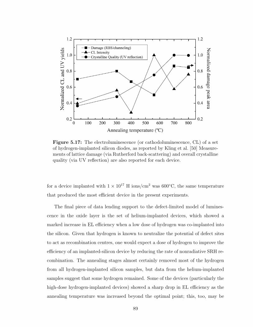
Figure 5.17: The electroluminescence (or cathodoluminescence, CL) of a setof hydrogen-implanted silicon diodes, as reported by Kling et al. [50] Measure-ments of lattice damage (via Rutherford back-scattering) and overall crystallinequality (via UV reflection) are also reported for each device.
for a device implanted with 1 × 10¹⁷ H ions/cm2 was 600C, the same temperature
that produced the most efficient device in the present experiments.
The final piece of data lending support to the defect-limited model of lumines-
cence in the oxide layer is the set of helium-implanted devices, which showed a
marked increase in EL efficiency when a low dose of hydrogen was co-implanted into
the silicon. Given that hydrogen is known to neutralize the potential of defect sites
to act as recombination centres, one would expect a dose of hydrogen to improve the
efficiency of an implanted-silicon device by reducing the rate of nonradiative SRH re-
combination. The annealing stages almost certainly removed most of the hydrogen
from all hydrogen-implanted silicon samples, but data from the helium-implanted
samples suggest that some hydrogen remained. Some of the devices (particularly the
high-dose hydrogen-implanted devices) showed a sharp drop in EL efficiency as the
annealing temperature was increased beyond the optimal point; this, too, may be
89

related to hydrogen loss. Such assertions are again supported by Kling et al., who
measured the hydrogen content of their devices as a function of annealing tempera-
ture [50]. Their results are shown in Figure 5.18; they suggest that as much as 40%
of the implanted hydrogen may remain in the silicon layer after annealing at 600C.
Cooke et al., who measured hydrogen content in their devices via a similar method,
reported much lower hydrogen retention (on the order of 5 to 10%) for the same
annealing temperatures; they, too, saw a correlation between hydrogen content and
EL efficiency from their silicon devices [83]. The time-resolved decay in EL efficiency
that was observed from many of the devices may also be attributed to hydrogen loss
(from Ohmic heating, for example), but there is too little data regarding the EL
decay to draw any firm conclusions on this point. The increase in the unimplanted
device’s efficiency over time also remains unexplained.
90

Figure 5.18: The hydrogen content of hydrogen-implanted devices preparedby Kling et al. as a function of annealing temperature [50]. The curves rele-vant to the present research are those for oxide-capped silicon (the top two inthe legend), where the oxide was not removed prior to annealing and EL mea-surements. All capped-silicon measurements were performed via elastic recoildetection (ERD), using a 2.0 MeV He+ beam.
91

Chapter 6
Conclusion
This thesis describes the fabrication of electroluminescent (EL) silicon diodes
using plasma ion implantation (PII) with the light elements hydrogen, helium, and
deuterium. The characterization and analysis of these devices were carried out chiefly
through measurements of their light emission. The motivation for this work, as
discussed in Chapter 1, is the development of CMOS-compatible light sources for
use in integrated optoelectronics applications. Plasma ion implantation would be an
excellent candidate process for fabricating such devices due to its high production
volume, low cost, and proven compatibility with existing semiconductor processing
techniques. Implantation with light ions was specifically chosen to build on promising
preliminary results from hydrogen-implanted devices fabricated by J. T. Steenkamp
(a former M. Sc. student) and James Mantyka (a former summer student). In
support of the main research, a numerical algorithm was devised to analyze Langmuir
probe data and estimate the plasma density using as few assumptions as possible.
Custom software packages were developed to facilitate the speedy analysis of both
probe data and spectroscopic measurements. Custom electronics, including a digital
pulse generator and the sweeping power supply for the Langmuir probe, were built
and tested. This equipment is described in Chapter 4 of the thesis. The remainder
of this Chapter will discuss the silicon devices that were fabricated and tested with
this equipment as well as the prospects for making more efficient silicon LEDs with
this technique.
92

6.1 Fabricated Devices
Chapter 5 describes the electrical, photometric, and spectroscopic measurements
performed on the ion-implanted silicon devices created over the course of the project.
Most ion-implanted devices were found to be electroluminescent, as was a device
made out of unimplanted silicon. Measurements were taken from a commercial LED
in order to estimate the devices’ external quantum efficiencies, which were typically
on the order of 10−6. Measurements of each device’s EL spectrum suggested that
their light emission mechanisms were similar, if not identical. It was concluded
that the luminescence from both implanted and unimplanted devices was caused by
radiative recombinations within the native oxide layer between the implanted silicon
and the semitransparent gold contact.
The ion dose, ion species, and post-implantation annealing temperature were
all found to affect the measured efficiency: a higher dose of ions, coupled with
the appropriate annealing temperature, increased the EL efficiency of several ion-
implanted devices well beyond the value measured from the unimplanted device. The
external quantum efficiency of the best device was measured as 4.2× 10⁻⁶, which is
nearly five times the unimplanted device’s efficiency of 8.6×10⁻⁷. Additional lattice
damage during implantation, which was induced by implanting heavier deuterium
ions in place of hydrogen, reduced the measured efficiency. The increase in efficiency
with dose was attributed to structure formation on the silicon surface during the
annealing stages, while the reduction in efficiency with damage was attributed to
an increase in the nonradiative Shockley-Read-Hall recombination rate within the
implanted silicon layer. Hydrogenation of helium-implanted devices was found to
improve EL efficiency by up to a factor of 4 when compared with devices implanted
with only helium; this effect was attributed to hydrogen passivation of dangling
bonds within the damaged silicon layer. The loss of hydrogen due to device heating
was cited as a possible cause of the decay observed in many devices’ EL efficiencies
over time.
93

6.2 Potential Applications
Based on the results reported in this thesis, several issues would have to be addressed
before useful silicon LEDs could be fabricated for computing or communications
applications. First, the efficiency of the devices was quite low: given a current density
of 2.5 A/cm2 and a device size of 1 mm2 (for an integrated, monolithic LED), the
best device produced in this research would induce a photocurrent between 10 and
50 nA (at best) in a high-grade silicon photodetector [5,6]. Additional components,
such as the wide-band amplifier described in [84], would be necessary to amplify this
signal to useful levels.
Second, the bias voltages needed to induce detectable EL in the devices studied
here were fairly high: greater than 10 volts in most cases. This is not an insur-
mountable problem; voltages this high or higher are often used in standard CMOS
technologies with nominal voltages of 5 volts or less. However, the use of a higher
voltage does introduce technical problems that require special design techniques to
address [85]. Heating due to the flow of current may also be an issue: the devices
studied here operated best at a current density between 1.5-2.5 A/cm2, which for a
device with an area of 1 mm2 would mean a total current of 15-25 mA and power
dissipation of roughly 240 mW. Finally, the frequency range of the LEDs produced in
the present experiment remains unknown; if the relaxation time of the luminescent
centres is too high, the LEDs produced here would not be able to effectively transmit
digital signals at the high frequencies (GHz range) required by modern computing.
Although the issues listed above cast some doubt on the applicability of this
research to the problems outlined in Chapter 1, the development of useful silicon
LEDs remains a possibility. Additional research in silicon (or silicon-oxide) electro-
luminescence is expected to refine the fabrication process; judging by the variance
between devices reported here, the EL efficiency of silicon devices might be improved
by an order of magnitude or more in this way. Meanwhile, the technology of CMOS-
compatible amplifiers and photodetectors continues to improve each year. However,
the prospects for creating a true silicon laser, which would necessarily require pop-
94

ulation inversion in the luminescent centres and optical gain within the luminescent
material, remain uncertain.
6.3 Future Work
The findings and conclusions in this thesis suggest a number of avenues of investiga-
tion for future researchers in this field. These include:
1. Varying the oxide thickness by thermal treatment of the silicon wafer;
2. Etching away the oxide completely before fabricating a silicon LED, to study
any luminescence that might originate from beneath the oxide layer;
3. Studying the effect of impurities in the silicon wafer on device luminescence,
possibly through the use of gettering techniques;
4. The use of different metal and dopant combinations, such as aluminum on n-
type silicon, or transparent conductors such as indium tin oxide (ITO) or zinc
oxide (ZO); and
5. The use of more characterization techniques to thoroughly probe the material
and structural properties of the silicon LEDs; these could include
(a) Atomic force microscopy (AFM), to study surface blistering;
(b) Electron paramagnetic resonance (EPR) spectroscopy, to measure the
damage distribution within the ion-implanted silicon;
(c) Elastic recoil detection (ERD) and/or secondary ion mass spectroscopy
(SIMS) to measure the oxygen and hydrogen content of the devices; and
(d) Transmission electron microscopy (TEM), to obtain images of the internal
structure of the implanted device, particularly the cavities and bubbles
that form after implantation.
95

References
[1] R. Ho, K. W. Mai, and M. A. Horowitz, “The future of wires,” Proc. IEEE,vol. 89, no. 4, pp. 490–504, 2001.
[2] M. Haurylau, G. Chen, H. Chen, J. Zhang, N. A. Nelson, D. H. Albonesi, E. G.Friedman, and P. M. Fauchet, “On-chip optical interconnect roadmap: Chal-lenges and critical directions,” IEEE J. Sel. Top. Quantum Electron., vol. 12,no. 6, pp. 1699–1705, 2006.
[3] H. Rong, R. Jones, A. Liu, O. Cohen, D. Hak, A. Fang, and M. Paniccia, “Acontinuous-wave Raman silicon laser,” Nature, vol. 433, no. 7027, pp. 725–728,2005.
[4] Q. Xu, B. Schmidt, S. Pradhan, and M. Lipson, “Micrometre-scale siliconelectro-optic modulator,” Nature, vol. 435, no. 7040, pp. 325–327, 2005.
[5] M. K. Emsley, O. Dosunmu, and M. S. Unlu, “High-speed resonant-cavity-enhanced silicon photodetectors on reflecting silicon-on-insulator substrates,”IEEE Photonics Technol. Lett., vol. 14, no. 4, pp. 519–521, 2002.
[6] M. Ghioni, F. Zappa, V. P. Kesan, and J. Warnock, “A VLSI-compatible high-speed silicon photodetector for optical data link applications,” IEEE Trans.Electron Devices, vol. 43, no. 7, pp. 1054–1060, 1996.
[7] N. Savage, “Linking with light,” IEEE Spectr., vol. 39, no. 8, pp. 32–36, 2002.
[8] P. M. Fauchet, “Photoluminescence and electroluminescence from porous sili-con,” J. Lumin., vol. 70, no. 1-6, pp. 294–309, 1996.
[9] O. Jambois, H. Rinnert, X. Devaux, and M. Vergnat, “Photoluminescence andelectroluminescence of size-controlled silicon nanocrystallites embedded in SiO2
thin films,” J. Appl. Phys., vol. 98, no. 4, pp. 046 105–3, 2005.
[10] J. Palm, F. Gan, B. Zheng, J. Michel, and L. C. Kimerling, “Electroluminescenceof erbium-doped silicon,” Phys. Rev. B, vol. 54, no. 24, pp. 17 603–17 615, 1996.
[11] G. F. Cerofolini, L. Meda, R. Balboni, F. Corni, S. Frabboni, G. Ottaviani,R. Tonini, M. Anderle, and R. Canteri, “Hydrogen-related complexes as thestressing species in high-fluence, hydrogen-implanted, single-crystal silicon,”Phys. Rev. B, vol. 46, no. 4, pp. 2061–2070, 1992.
96

[12] P. K. Chu and N. W. Cheung, “Microcavity engineering by plasma immersionion implantation,” Mater. Chem. Phys., vol. 57, no. 1, pp. 1–16, 1998.
[13] W. Liu, S. C. H. Kwok, R. K. Y. Fu, P. K. Chu, T. F. Hung, Z. Xu, C. Lin,K. F. Li, H. L. Tam, and K. W. Cheah, “Room-temperature electroluminescencefrom H-plasma-implanted silicon,” Semicond. Sci. Technol., vol. 18, no. 12, pp.L55–L58, 2003.
[14] M. P. Bradley, P. R. Desautels, D. Hunter, and M. Risch, “Silicon electrolu-minescent device production via plasma ion implantation,” Phys. Status Solidi(c), vol. 6, no. S1, pp. S206–S209, 2009.
[15] P. R. Desautels, M. P. Bradley, J. T. Steenkamp, and J. Mantyka, “Electrolu-minescence in plasma ion implanted silicon,” Phys. Status Solidi (a), vol. 206,no. 5, pp. 985–988, 2009.
[16] J. R. Chelikowsky and M. L. Cohen, “Electronic structure of silicon,” Phys.Rev. B, vol. 10, no. 12, pp. 5095–5107, 1974.
[17] Bilbao Crystallographic Server. Electronic database. [Online]. Available:http://www.cryst.ehu.es/
[18] W. Shockley and W. T. Read, “Statistics of the Recombinations of Holes andElectrons,” Phys. Rev., vol. 87, no. 5, pp. 835–842, 1952.
[19] C. Kittel, Introduction to Solid State Physics, 8th ed. New York: Wiley, 2005.
[20] D. Schroder, “Carrier lifetimes in silicon,” IEEE Trans. Electron Devices,vol. 44, no. 1, pp. 160–170, 1997.
[21] H. Schlangenotto, H. Maeder, and W. Gerlach, “Temperature dependence of theradiative recombination coefficient in silicon,” Phys. Status Solidi (a), vol. 21,no. 1, pp. 357–367, 1974.
[22] R. J. Nelson and R. G. Sobers, “Minority-carrier lifetimes and internal quantumefficiency of surface-free GaAs,” J. Appl. Phys., vol. 49, no. 12, pp. 6103–6108,1978.
[23] G. B. Lush, “B-coefficient in n-type GaAs,” Sol. Energy Mater. Sol. Cells,vol. 93, no. 8, pp. 1225–1229, 2009.
[24] J. Dziewior and W. Schmid, “Auger coefficients for highly doped and highlyexcited silicon,” Appl. Phys. Lett., vol. 31, no. 5, pp. 346–348, 1977.
[25] P. P. Altermatt, J. Schmidt, G. Heiser, and A. G. Aberle, “Assessment and pa-rameterisation of Coulomb-enhanced Auger recombination coefficients in lowlyinjected crystalline silicon,” J. Appl. Phys., vol. 82, no. 10, pp. 4938–4944, 1997.
[26] M. J. Kerr and A. Cuevas, “General parameterization of Auger recombinationin crystalline silicon,” J. Appl. Phys., vol. 91, no. 4, pp. 2473–2480, 2002.
97

[27] A. Wilk, A. Kovsh, S. Mikhrin, C. Chaix, I. Novikov, M. Maximov, Y. Sh-ernyakov, V. Ustinov, and N. Ledentsov, “High-power InAs/GaInAs/GaAs QDlasers grown in a multiwafer MBE production system,” J. Cryst. Growth, vol.278, no. 1-4, pp. 335–341, 2005.
[28] D. Bimberg, “Quantum dots for lasers, amplifiers and computing,” J. Phys. D,vol. 38, no. 13, pp. 2055–2058, 2005.
[29] M. Kittler, T. Arguirov, A. Fischer, and W. Seifert, “Silicon-based light emissionafter ion implantation,” Opt. Mater., vol. 27, no. 5, pp. 967–972, 2005.
[30] H. Bleichner, P. Jonsson, N. Keskitalo, and E. Nordlander, “Temperature andinjection dependence of the Shockley–Read–Hall lifetime in electron irradiatedn-type silicon,” J. Appl. Phys., vol. 79, no. 12, pp. 9142–9148, 1996.
[31] L. T. Canham, “Silicon quantum wire array fabrication by electrochemical andchemical dissolution of wafers,” Appl. Phys. Lett., vol. 57, no. 10, pp. 1046–1048,1990.
[32] V. Lehmann and U. Gosele, “Porous silicon formation: A quantum wire effect,”Appl. Phys. Lett., vol. 58, no. 8, pp. 856–858, 1991.
[33] A. G. Cullis, L. T. Canham, and P. D. J. Calcott, “The structural and lumines-cence properties of porous silicon,” J. Appl. Phys., vol. 82, no. 3, pp. 909–965,1997.
[34] M. S. Hybertsen, “Absorption and emission of light in nanoscale silicon struc-tures,” Phys. Rev. Lett., vol. 72, no. 10, pp. 1514–1517, 1994.
[35] B. Delley and E. F. Steigmeier, “Size dependence of band gaps in silicon nanos-tructures,” Appl. Phys. Lett., vol. 67, no. 16, pp. 2370–2372, 1995.
[36] M. V. Wolkin, J. Jorne, P. M. Fauchet, G. Allan, and C. Delerue, “ElectronicStates and Luminescence in Porous Silicon Quantum Dots: The Role of Oxy-gen,” Phys. Rev. Lett., vol. 82, no. 1, pp. 197–200, 1999.
[37] D. Bisero, F. Corni, C. Nobili, R. Tonini, G. Ottaviani, C. Mazzoleni, andL. Pavesi, “Visible photoluminescence from He-implanted silicon,” Appl. Phys.Lett., vol. 67, no. 23, pp. 3447–3449, 1995.
[38] L. Wang, R. K. Y. Fu, X. Zeng, P. K. Chu, W. Y. Cheung, and S. P. Wong,“Damage in hydrogen plasma implanted silicon,” J. Appl. Phys., vol. 90, no. 4,pp. 1735–1739, 2001.
[39] C. Delerue, G. Allan, and M. Lannoo, “Theoretical aspects of the luminescenceof porous silicon,” Phys. Rev. B, vol. 48, no. 15, pp. 11 024–11 036, 1993.
[40] M. Morita, T. Ohmi, E. Hasegawa, M. Kawakami, and M. Ohwada, “Growth ofnative oxide on a silicon surface,” J. Appl. Phys., vol. 68, no. 3, pp. 1272–1281,1990.
98

[41] L. Heikkila, T. Kuusela, and H. P. Hedman, “Electroluminescence in Si/SiO2
layer structures,” J. Appl. Phys., vol. 89, no. 4, pp. 2179–2184, 2001.
[42] J. H. Stathis and M. A. Kastner, “Time-resolved photoluminescence in amor-phous silicon dioxide,” Phys. Rev. B, vol. 35, no. 6, pp. 2972–2979, 1987.
[43] A. P. Baraban, E. A. Semykina, and M. B. Vaniouchov, “Understanding electro-luminescence from thin silicon dioxide films,” Semicond. Sci. Technol., vol. 15,pp. 546–550, 2000.
[44] G. Qin and Y. Jia, “Mechanism of the visible luminescence in porous silicon,”Solid State Commun., vol. 86, no. 9, pp. 559–563, 1993.
[45] G. Qin and G. G. Qin, “Theory on the quantum confinement-luminescencecenter model for nanocrystalline and porous Si,” J. Appl. Phys., vol. 82, no. 5,pp. 2572–2579, 1997.
[46] G. G. Qin, Y. M. Huang, J. Lin, L. Z. Zhang, B. Q. Zong, and B. R. Zhang,“Electroluminescence from Au/native oxide/p-Si and its correlation to that fromAu/porous Si,” Solid State Commun., vol. 94, no. 8, pp. 607–612, 1995.
[47] G. Dearnaley, “Ion Implantation,” Annu. Rev. Mater. Sci., vol. 4, pp. 93–123,1974.
[48] P. K. Chu, S. Qin, C. Chan, N. W. Cheung, and L. A. Larson, “Plasma im-mersion ion implantation–a fledgling technique for semiconductor processing,”Mat. Sci. Eng. R., vol. 17, no. 6-7, pp. 207–280, 1996.
[49] N. Cheung, “Plasma immersion ion implantation for semiconductor processing,”Mater. Chem. Phys., vol. 46, no. 2-3, pp. 132–139, 1996.
[50] A. Kling, J. C. Soares, A. Rodrguez, T. Rodrguez, M. Avella, and J. Jimnez,“Effect of thermal annealing on the optical and structural properties of siliconimplanted with a high hydrogen fluence,” Nucl. Instrum. Methods Phys. Res.B, vol. 242, no. 1-2, pp. 650–652, 2006.
[51] L. Pavesi, G. Giebel, R. Tonini, F. Corni, C. Nobili, and G. Ottaviani, “Visibleluminescence from silicon by hydrogen implantation and annealing treatments,”Appl. Phys. Lett., vol. 65, no. 4, pp. 454–456, 1994.
[52] F. F. Chen, Introduction to Plasma Physics and Controlled Fusion, 2nd ed.New York: Springer, 2006.
[53] M. Risch and M. Bradley, “Predicted depth profiles for nitrogen-ion implanta-tion into gallium arsenide,” Phys. Status Solidi (c), vol. 5, no. 4, pp. 939–942,2008.
[54] M. Risch, “The Promise of Nitrogen Plasma Implanted Gallium Arsenide forBand Gap Engineering,” Master’s thesis, University of Saskatchewan, Dept. ofPhysics and Eng. Physics, 2008.
99

[55] M. A. Lieberman, “Model of plasma immersion ion implantation,” J. Appl.Phys., vol. 66, no. 7, pp. 2926–2929, 1989.
[56] M. A. Lieberman and A. J. Lichtenberg, Principles of Plasma Discharges andMaterials Processing. New York: Wiley-Interscience, 2005.
[57] C. D. Child, “Discharge from hot CaO,” Phys. Rev. (Series I), vol. 32, pp.492–511, 1911.
[58] K. S. Suraj and S. Mukherjee, “Effect of ion neutral collisions on the ion andneutral velocity distribution on negatively biased electrodes,” Surf. Coat. Tech-nol., vol. 196, no. 1-3, pp. 267–270, 2005.
[59] G. W. McClure, “High-Voltage Glow Discharges in D2 Gas: Diagnostic Mea-surements,” Phys. Rev., vol. 124, no. 4, pp. 969–982, 1961.
[60] P. M. Stier and C. F. Barnett, “Charge exchange cross sections of hydrogen ionsin gases,” Phys. Rev., vol. 103, no. 4, pp. 896–907, 1956.
[61] C. F. Barnett and P. M. Stier, “Charge exchange cross sections for helium ionsin gases,” Phys. Rev., vol. 109, no. 2, pp. 385–390, 1958.
[62] A. Anders, Handbook of Plasma Immersion Ion Implantation and Deposition.New York: Wiley-Interscience, 2000.
[63] H. M. Mott-Smith and I. Langmuir, “The Theory of Collectors in GaseousDischarges,” Phys. Rev., vol. 28, no. 4, pp. 727–763, 1926.
[64] I. H. Hutchinson, Principles of Plasma Diagnostics, 2nd ed. Cambridge Uni-versity Press, 2002.
[65] L. Tonks and I. Langmuir, “A General Theory of the Plasma of an Arc,” Phys.Rev., vol. 34, no. 6, pp. 876–922, 1929.
[66] S. H. Lam, “Unified Theory for the Langmuir Probe in a Collisionless Plasma,”Phys. Fluids, vol. 8, no. 1, pp. 73–87, 1965.
[67] K. U. Riemann, “Kinetic theory of the plasma sheath transition in a weaklyionized plasma,” Phys. Fluids, vol. 24, no. 12, pp. 2163–2172, 1981.
[68] F. F. Chen, “Langmuir probe analysis for high density plasmas,” Phys. Plasmas,vol. 8, no. 6, pp. 3029–3041, 2001.
[69] S. Qin, C. Chan, and Z. Jin, “Plasma immersion ion implantation model in-cluding multiple charge state,” J. Appl. Phys., vol. 79, no. 7, pp. 3432–3437,1996.
[70] C. J. T. Steenkamp, “High Power Solid State Modulator for Plasma Ion Im-plantation,” Master’s thesis, University of Saskatchewan, Dept. of Physics andEng. Physics, 2006.
100

[71] J. F. Ziegler, J. P. Biersack, and U. Littmark, The Stopping and Range of Ionsin Solids. New York: Pergamon, 1985.
[72] S. Nunomura and M. Kondo, “Characterization of high-pressure capacitivelycoupled hydrogen plasmas,” J. Appl. Phys., vol. 102, no. 9, pp. 093 306–7, 2007.
[73] M. Fitzgerald, J. Khachan, and S. Bosi, “Relative densities of hydrogen ionspecies in a hollow cathode glow discharge,” Eur. Phys. J. D, vol. 39, no. 1, pp.35–39, 2006.
[74] M. Tuszewski and J. A. Tobin, “The accuracy of Langmuir probe ion densitymeasurements in low-frequency (RF) discharges,” Plasma Sources Sci. Technol.,vol. 5, no. 4, pp. 640–647, 1996.
[75] C. J. T. Steenkamp and M. P. Bradley, “Active Charge/Discharge IGBT Modu-lator for Marx Generator and Plasma Applications,” IEEE Trans. Plasma Sci.,vol. 35, no. 2, pp. 473–478, 2007.
[76] G. A. Emmert, “Model for expanding sheaths and surface charging at dielectricsurfaces during plasma source ion implantation,” J. Vac. Sci. Technol. B, vol. 12,pp. 880–883, 1994.
[77] P. B. Johnson and R. W. Christy, “Optical Constants of the Noble Metals,”Phys. Rev. B, vol. 6, no. 12, pp. 4370–4379, 1972.
[78] J. Geist, “Silicon (Si) revisited (1.1-3.1 eV),” in Handbook of Optical Constantsof Solids, E. D. Palik, Ed. San Diego: Academic, 1998, vol. III, pp. 519–529.
[79] GNUPLOT. Open-source software. [Online]. Available:http://www.gnuplot.info
[80] C. P. Ho, J. D. Plummer, S. E. Hansen, and R. W. Dutton, “VLSI ProcessModeling - SUPREM III,” IEEE Trans. Electron Devices, vol. 30, no. 11, pp.1438–1453, 1983.
[81] G. F. Bai, Y. Q. Wang, Z. C. Ma, W. H. Zong, and G. G. Qin, “Electrolumi-nescence from Au/native silicon oxide layer/p+ Si and Au/native silicon oxidelayer/n+ Si structures under reverse biases,” J. Phys. Condens. Matter, vol. 10,no. 44, pp. L717–L721, 1998.
[82] J. Yuan and D. Haneman, “Visible electroluminescence from native SiO2 onn-type Si substrates,” J. Appl. Phys., vol. 86, no. 4, pp. 2358–2360, 1999.
[83] D. W. Cooke, B. L. Bennett, E. H. Farnum, W. L. Hults, K. E. Sickafus, J. F.Smith, J. L. Smith, T. N. Taylor, P. Tiwari, and A. M. Portis, “SiOx lumines-cence from light-emitting porous silicon,” Appl. Phys. Lett., vol. 68, no. 12, pp.1663–1665, 1996.
101

[84] C.-W. Kim, M.-S. Kang, P. T. Anh, H.-T. Kim, and S.-G. Lee, “An Ultra-Wideband CMOS Low Noise Amplifier for 35-GHz UWB System,” IEEE J.Solid-State Circuits, vol. 40, no. 2, pp. 544–547, 2005.
[85] H. Ballan and M. Declercq, High voltage devices and circuits in standard CMOStechnologies. New York: Springer, 1999.
[86] International Commission on Illumination (CIE). CIE 1964 SupplementaryStandard Colorimetric Observer data. Free document. [Online]. Available:http://www.cie.co.at/main/freepubs.html
102

Appendix A
Quantum Efficiency Calculation
The SpectraPro 300i spectrometer and attached PI-MAX camera described inSection 4.9 measure light in CCD counts, not actual photons. Although this issufficient for comparisons between devices, a reasonable estimate of each device’sexternal quantum efficiency is needed in order to evaluate the devices’ potentialapplicability to real problems. The general formula for the efficiency ηx, in terms ofknown or measurable quantities, is
ηx =NCT
β·G · e
ID, (A.1)
where NCT is the total number of counts detected per second on the CCD arrayof the camera, β is the detector efficiency (counts per photon), ID is the drivecurrent through the electroluminescent device, and G is a geometric factor relatingthe detected light to the total emitted light. NCT is a measured quantity, and IDis a known parameter; therefore, only β and G need to be determined in order tocalculate ηx.
A.1 Geometric Factor
Consider the setup presented in Figure A.1: a light source of area AD is placed adistance L from the entrance slit of a spectrometer or photometer; the slit has areaAslit. The light source radiates photons through its viewing angle θ, delivering powerto the surface of the spherical cap subtended by θ. It is assumed in this calculationthat the irradiance (power per unit area) delivered to the spherical cap is uniform.It is also assumed that the detector behind the slit can only record light that isnormally incident on the slit. The area of the entrance slit of the SpectraPro 300i is4 mm2.
Under this arrangement, the slit can only receive light from an area on the emitterequal to its own area Aslit. Furthermore, the slit area receives only a fraction of thetotal light emitted from this small area, equal to the ratio of the slit area to the areaof the spherical cap at radius L. The area of a spherical cap of radius L, subtendedby the angle θ, is
Acap = 4πL2 sin2
(θ
4
), (A.2)
so the ratio of detected light to the sum of all light emitted by the device (thegeometric factor G) must be
G = 4πL2 sin2
(θ
4
)AD
A2slit
. (A.3)
103

Figure A.1: The geometry of the present photometry and spectrometry mea-surements. In general, only a small portion of the total area AD of the lightsource is visible to the entrance slit of the spectrometer, positioned at a dis-tance L from the emitter’s surface. It is assumed that this portion of the lightsource radiates photons uniformly across the viewing angle θ, distributing itspower evenly over the area of the subtended spherical cap of radius L.
For spectrometry and photometry measurements with implanted-silicon devices, thevalue of L is 25 mm, the value of θ is assumed to be 180, and the emitter area AD
varies from device to device. The setup used to determine the detector efficiency wasslightly different and will be described in the next section.
A.2 Detector Efficiency
To determine the efficiency of the spectrometer - the number of counts detectedper photon received - the entrance slit was illuminated with a commercial red LED(a LUMEX SD-LX5093HD) and measured its output. The LED was positioned asshown in Figure A.1 with the distance L equal to 12.5 mm. The datasheet for theSD-LX5093HD gives the viewing angle θ as 60, and it is assumed that the light-emitting die within the diode is the same size or smaller than the slit width, soAD = Aslit in Eq. A.3 for this measurement.
The luminous intensity of the SD-LX5093HD is given as 0.005 candelas. Thecandela is a base SI unit defined as the luminous intensity of a source that emits
104
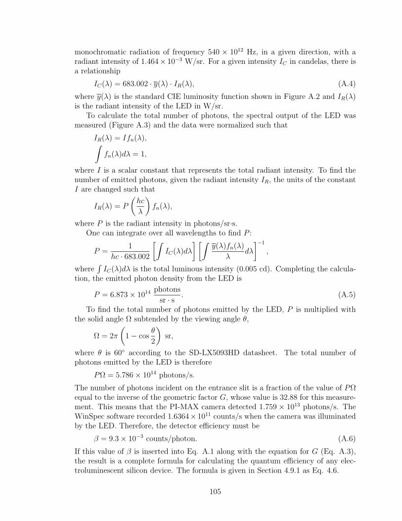
monochromatic radiation of frequency 540 × 1012 Hz, in a given direction, with aradiant intensity of 1.464× 10⁻³ W/sr. For a given intensity IC in candelas, there isa relationship
IC(λ) = 683.002 · y(λ) · IR(λ), (A.4)
where y(λ) is the standard CIE luminosity function shown in Figure A.2 and IR(λ)is the radiant intensity of the LED in W/sr.
To calculate the total number of photons, the spectral output of the LED wasmeasured (Figure A.3) and the data were normalized such that
IR(λ) = Ifn(λ),∫fn(λ)dλ = 1,
where I is a scalar constant that represents the total radiant intensity. To find thenumber of emitted photons, given the radiant intensity IR, the units of the constantI are changed such that
IR(λ) = P
(hc
λ
)fn(λ),
where P is the radiant intensity in photons/sr·s.One can integrate over all wavelengths to find P :
P =1
hc · 683.002
[∫IC(λ)dλ
] [∫y(λ)fn(λ)
λdλ
]−1
,
where∫IC(λ)dλ is the total luminous intensity (0.005 cd). Completing the calcula-
tion, the emitted photon density from the LED is
P = 6.873× 10¹⁴ photons
sr · s. (A.5)
To find the total number of photons emitted by the LED, P is multiplied withthe solid angle Ω subtended by the viewing angle θ,
Ω = 2π
(1− cos
θ
2
)sr,
where θ is 60 according to the SD-LX5093HD datasheet. The total number ofphotons emitted by the LED is therefore
PΩ = 5.786× 10¹⁴ photons/s.
The number of photons incident on the entrance slit is a fraction of the value of PΩequal to the inverse of the geometric factor G, whose value is 32.88 for this measure-ment. This means that the PI-MAX camera detected 1.759 × 10¹³ photons/s. TheWinSpec software recorded 1.6364× 10¹¹ counts/s when the camera was illuminatedby the LED. Therefore, the detector efficiency must be
β = 9.3× 10⁻³ counts/photon. (A.6)
If this value of β is inserted into Eq. A.1 along with the equation for G (Eq. A.3),the result is a complete formula for calculating the quantum efficiency of any elec-troluminescent silicon device. The formula is given in Section 4.9.1 as Eq. 4.6.
105

Figure A.2: The standard CIE photopic luminosity function, representingthe sensitivity of the average human eye to light in the visible spectrum in awell-lit environment. The y-axis is unitless and the function is normalized suchthat the maximum at 555 nm is exactly 1. After [86].
Figure A.3: The spectrum of a LUMEX SD-LX5093HD red LED, as measuredby the SpectraPro 300i spectrometer and PI-MAX camera. The data shownhere are not yet normalized.
106

Appendix B
Custom Devices and Tools
B.1 Digital Pulse Generator
Figure B.1: The operational flowchart for the custom digital pulse generatorused to trigger high-voltages pulses from the Marx stages. Prompting andfeedback to the user is provided through an LCD unit mounted on the frontpanel of the pulse generator. The operation of the circuit is controlled by aPIC18F4520 microcontroller.
107

B.2 Langmuir Probe Power Supply
The Langmuir probe power supply is designed to produce a stable triangle-wave(sawtooth) voltage signal with user-controlled amplitude, frequency, and DC offsetvoltage. The circuit used to generate this signal is composed of two stages: theramp generator (Figure B.2), which produces a small-signal triangle wave; and theamplifier (Figure B.3), which amplifies the signal to useful levels. The output iscontrolled by three variable resistors, RFREQ, RAMP , and RDCO, whose values canbe set in the range 0 → 100kΩ. Their relations to the frequency (f), peak-to-peakvoltage (Vpeak−peak), and DC offset voltage (VDC) are given by the following equations:
f ∝ 1
4CR2
(RFSET +RFREQ
R1
),
Vpeak−peak ∝(
22kΩ
22kΩ +RAMP
),
VDC ∝(
1− 47kΩ +RDCO
97kΩ
).
The constants of proportionality for each quantity are on the order of 1.0 (generallybetween 0.5 and 2.0); they should be exactly 1.0 in theory, but non-idealities in thereal circuit cause deviations from the predicted behaviour. I do not consider this asignificant flaw, since the output is stable over time (corrections due to non-idealitiesare constant) and the controlling resistors may be adjusted until one obtains thedesired waveform.
B.3 Software Screenshots
Figures B.4 and B.5 are screenshots taken of the custom software described in Sec-tions 4.6 and 4.9.2 of the thesis. Both pieces of software were programmed in C++and employ the Qt package to implement the graphical interface.
108

Figure B.2: The circuit used to generate a linear voltage sweep for the Lang-muir probe. The charging and discharging of capacitor C, linked to an op-ampintegrator (OPA), produces a series of linear voltage ramps. The polarity ofthe capacitor is periodically reversed by a comparator (OPB). The frequencyof this oscillation can be controlled via resistor RFREQ. The summing amplifier(OPC) allows the user to change the amplitude of the sweep and add a DCoffset by manipulating resistors RAMP and RDCO, respectively.
109
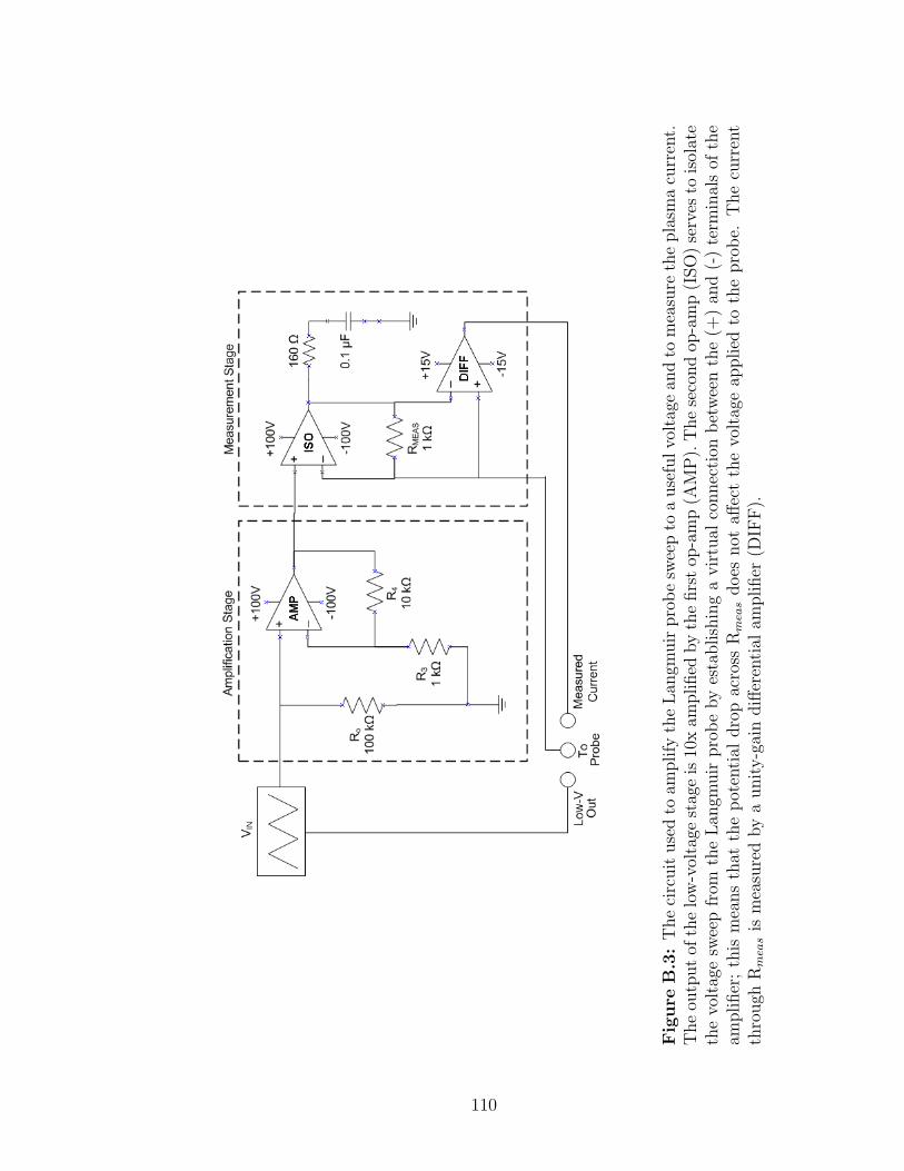
Fig
ure
B.3
:T
he
circ
uit
use
dto
amplify
the
Lan
gmuir
pro
be
swee
pto
ause
fulvo
ltag
ean
dto
mea
sure
the
pla
sma
curr
ent.
The
outp
ut
ofth
elo
w-v
olta
gest
age
is10
xam
plified
by
the
firs
top
-am
p(A
MP
).T
he
seco
nd
op-a
mp
(ISO
)se
rves
tois
olat
eth
evo
ltag
esw
eep
from
the
Lan
gmuir
pro
be
by
esta
blish
ing
avir
tual
connec
tion
bet
wee
nth
e(+
)an
d(-
)te
rmin
als
ofth
eam
plifier
;th
ism
eans
that
the
pot
enti
aldro
pac
ross
Rm
eas
does
not
affec
tth
evo
ltag
eap
plied
toth
epro
be.
The
curr
ent
thro
ugh
Rm
eas
ism
easu
red
by
aunit
y-g
ain
diff
eren
tial
amplifier
(DIF
F).
110

Fig
ure
B.4
:T
he
QtP
lasm
aCon
sole
mai
nw
indow
.T
he
four
sub-w
indow
s,cl
ock
wis
efr
omth
eupp
erle
ft,
are:
INP
UT
,w
her
eth
euse
rpro
vid
esth
eso
ftw
are
wit
hre
quir
eddat
aan
din
put
file
s;O
UT
PU
T,w
her
eca
lcula
tion
step
s,er
ror
mes
sage
s,an
ddat
aplo
tsm
ayb
ere
vie
wed
;R
ESU
LT
S,
wher
efinal
resu
lts
are
show
nan
dca
nb
esa
ved
todis
k;
and
PA
RA
ME
TE
RS,
wher
eva
riou
sse
condar
yin
puts
toth
eco
de
may
be
revie
wed
and
modifi
ed.
111

Fig
ure
B.5
:T
he
Sp
ectr
alA
nal
yze
rm
ain
win
dow
.T
he
dat
ato
be
plo
tted
and
afe
wm
inor
par
amet
ers
are
input
toth
eupp
er-r
ight
pan
el.
The
plo
tit
self
issh
own
onth
eupp
er-l
eft.
Bel
owth
eplo
ttin
gpan
elis
the
Gau
ssia
nfit
man
ager
,fr
omw
hic
hth
euse
rdefi
nes
Gau
ssia
nfu
nct
ions
tob
eplo
tted
alon
gsid
eth
esp
ectr
aldat
a.T
he
pan
elon
the
bot
tom
-rig
ht
dis
pla
ys
the
reduce
dch
i-sq
uar
eva
lue
for
the
fit
and
allo
ws
the
use
rto
save
the
resu
lts
todis
k.
112