Fabrication of arbitrarily shaped silicon and silicon ... · PDF fileFabrication of...
8
Fabrication of arbitrarily shaped silicon and silicon oxide nanostructures using tip- based nanofabrication Huan Hu, Parsian K. Mohseni, Lei Pan, Xiuling Li, Suhas Somnath, Jonathan R. Felts, Mark A. Shannon, and William P. King Citation: Journal of Vacuum Science & Technology B 31, 06FJ01 (2013); doi: 10.1116/1.4831767 View online: http://dx.doi.org/10.1116/1.4831767 View Table of Contents: http://scitation.aip.org/content/avs/journal/jvstb/31/6?ver=pdfcov Published by the AVS: Science & Technology of Materials, Interfaces, and Processing Redistribution subject to AVS license or copyright; see http://scitation.aip.org/termsconditions. Download to IP: 132.250.22.11 On: Tue, 04 Mar 2014 17:32:05
Transcript of Fabrication of arbitrarily shaped silicon and silicon ... · PDF fileFabrication of...

Fabrication of arbitrarily shaped silicon and silicon oxide nanostructures using tip-based nanofabricationHuan Hu, Parsian K. Mohseni, Lei Pan, Xiuling Li, Suhas Somnath, Jonathan R. Felts, Mark A. Shannon, and
William P. King Citation: Journal of Vacuum Science & Technology B 31, 06FJ01 (2013); doi: 10.1116/1.4831767 View online: http://dx.doi.org/10.1116/1.4831767 View Table of Contents: http://scitation.aip.org/content/avs/journal/jvstb/31/6?ver=pdfcov Published by the AVS: Science & Technology of Materials, Interfaces, and Processing
Redistribution subject to AVS license or copyright; see http://scitation.aip.org/termsconditions. Download to IP: 132.250.22.11 On: Tue, 04 Mar 2014 17:32:05
Fabrication of arbitrarily shaped silicon and silicon oxide nanostructuresusing tip-based nanofabrication
Huan Hu, Parsian K. Mohseni, Lei Pan, and Xiuling LiDepartment of Electrical and Computer Engineering, University of Illinois at Urbana-Champaign, Urbana,Illinois 61801
Suhas Somnath, Jonathan R. Felts, Mark A. Shannon, and William P. Kinga)
Department of Mechanical Science and Engineering, University of Illinois at Urbana-Champaign, Urbana,Illinois 61801
(Received 14 June 2013; accepted 4 November 2013; published 22 November 2013)
The authors report fabrication of arbitrary shapes of silicon and silicon oxide nanostructures using
tip-based nanofabrication (TBN). A heated atomic force microscope (AFM) tip deposits molten
polymer on a substrate to form polymer nanostructures that serve as etch mask to fabricate silicon
or silicon oxide nanostructures. The authors demonstrate how TBN can be combined with
conventional wet etching as well as metal-assisted chemical etching, in order to fabricate these
nanostructures. The size of the TBN-fabricated silicon nanostructures is around 200 nm. Silicon
nanostructures fabricated using metal-assisted chemical etch can have very smooth sidewalls
with, roughness as small as 2 nm. The authors show fabrication of arbitrary shapes of silicon and
silicon oxide nanostructures including those with curved and circular shapes. Our results show that
TBN using a heated AFM tip can function as an additive nanolithography technique with
minimum contamination, and is compatible with existing nanofabrication methods. VC 2013American Vacuum Society. [http://dx.doi.org/10.1116/1.4831767]
I. INTRODUCTION
Tip-based nanofabrication (TBN) uses a nanometer-scale
tip to interact with a sample to fabricate nanostructures.
TBN has the potential for fabricating nanostructures with
controlled size, shape, and orientation at precise substrate
locations and nanometer-scale precision and resolution.1 In
TBN, a tip can interact with the sample to fabricate nano-
structures, with the tip influencing the surface through any of
a number of mechanisms, including mechanical,2 electro-
chemical,3 optical,4 chemical diffusion,5 thermal,6 electrical
polarization,7 and plasma.8
Although TBN has many advantages, there are only a
few published articles that describe the use of TBN for
nanodevice fabrication.9–16 A key challenge to realizing
TBN-fabricated nanodevices is to incorporate TBN fabrication
steps with other processing steps. Unfortunately, most TBN
methods are not easily compatible with nanofabrication.17–22
For example, dip pen nanolithography (DPN) can fabricate sil-
icon nanostructures only when combined with intermediate
chemical processing steps. One publication showed the use of
DPN to fabricate gold nanostructures using DPN, and then
used these gold nanostructures as a masking step for subse-
quent etching.23 Oxidation-based TBN can fabricate silicon
oxide nanostructures with only a few nanometers in thickness
due to the slow oxidation rate. One publication showed that
the oxidation rate falls dramatically due to self-limiting behav-
ior resulting from the build-up stress and a reduction of electri-
cal field strength.24 To achieve device fabrication using TBN,
a key challenge is improved compatibility with silicon fabrica-
tion processes.
Here, we show that a heated AFM tip can deposit thick
polymer nanostructures and transfer the written structures
into both silicon and silicon oxide films in a one-step etching
process. Moreover, we show the flexibility of the technique
by demonstrating the fabrication of arbitrary shapes of solid
structures of silicon oxide. Our TBN method is compatible
with existing nanofabrication methods and especially suita-
ble for device fabrication.
II. EXPERIMENTAL AND RESULTS
A. Nanostructures formed using tip-basednanofabrication and wet chemical etching
Figure 1 shows the process used to fabricate silicon oxide
nanostructures by TBN. First, we grew a 50 nm thick silicon
oxide layer via thermal oxidation at 1000 �C for 80 min.
Then, a heated AFM tip deposited polystyrene (PS) on top of
the oxide layer via TBN. Following polymer deposition, we
etched the 50 nm thick silicon oxide layer by dipping
the sample into buffered hydrofluoric acid (BHF) for 60 s.
BHF etched the silicon oxide that was not masked by the PS
nanopatterns. The last step was to remove PS by acetone and
oxygen plasma reactive ion etching (RIE).
A key step in the process is to provide polymer ink onto
the cantilever tip and to then deliver the polymer ink onto
the surface. The polymer was loaded onto the cantilever tip
by bringing the heated AFM tip end onto a PS fiber. The
heated tip melted the PS, and then the PS flowed onto the
tip.25 After inking, we mounted the tip in an Asylum
Research MFP-3D AFM and scanned the tip along a pro-
grammed path with a constant force at a speed of
150 nm/s.25 A closed-loop feedback circuit maintained the
cantilever heater temperature at 260 �C.26 When the tip wasa)Electronic mail: [email protected]
06FJ01-1 J. Vac. Sci. Technol. B 31(6), Nov/Dec 2013 2166-2746/2013/31(6)/06FJ01/7/$30.00 VC 2013 American Vacuum Society 06FJ01-1
Redistribution subject to AVS license or copyright; see http://scitation.aip.org/termsconditions. Download to IP: 132.250.22.11 On: Tue, 04 Mar 2014 17:32:05
hot, the molten polymer would flow from the moving tip to
the substrate and form solid PS nanostructures.6 The force
between the tip and the substrate was maintained around 200
nN during the deposition. During heating, the tip-sample ad-
hesion force, measured by pulling the tip off of the surface,
was about 425 nN.
Figure 2(a) shows an AFM contact mode image of vari-
ous PS linear nanostructures deposited using the heated
AFM tip at different tip scanning speeds. The PS linear
nanostructures from right to left as shown in Fig. 2(a) are de-
posited by the heated AFM tip at 0.1, 0.2, 0.4, 0.6, 0.8, 1.0,
1.5, and 2.0 lm/s tip scanning speeds. Figure 2(b) summa-
rizes the PS nanostructures heights at different tip scanning
speeds. As the tip scanning speed increases, the deposited
polymer lines are thinner. This is consistent with a previous
publication, which showed that polymer deposition rate is
relatively independent from tip speed.25 Thus, a faster mov-
ing tip deposits less amount of polymer per unit length and
therefore produces a thinner line.
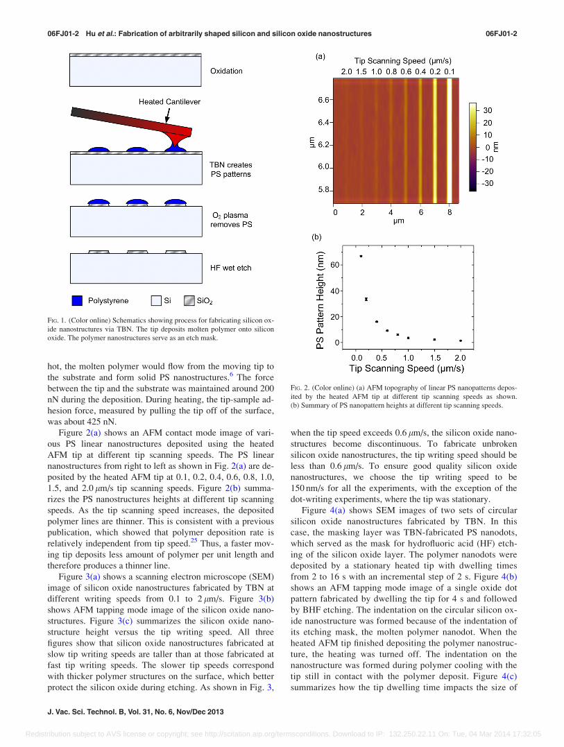
Figure 3(a) shows a scanning electron microscope (SEM)
image of silicon oxide nanostructures fabricated by TBN at
different writing speeds from 0.1 to 2 lm/s. Figure 3(b)
shows AFM tapping mode image of the silicon oxide nano-
structures. Figure 3(c) summarizes the silicon oxide nano-
structure height versus the tip writing speed. All three
figures show that silicon oxide nanostructures fabricated at
slow tip writing speeds are taller than at those fabricated at
fast tip writing speeds. The slower tip speeds correspond
with thicker polymer structures on the surface, which better
protect the silicon oxide during etching. As shown in Fig. 3,
when the tip speed exceeds 0.6 lm/s, the silicon oxide nano-
structures become discontinuous. To fabricate unbroken
silicon oxide nanostructures, the tip writing speed should be
less than 0.6 lm/s. To ensure good quality silicon oxide
nanostructures, we choose the tip writing speed to be
150 nm/s for all the experiments, with the exception of the
dot-writing experiments, where the tip was stationary.
Figure 4(a) shows SEM images of two sets of circular
silicon oxide nanostructures fabricated by TBN. In this
case, the masking layer was TBN-fabricated PS nanodots,
which served as the mask for hydrofluoric acid (HF) etch-
ing of the silicon oxide layer. The polymer nanodots were
deposited by a stationary heated tip with dwelling times
from 2 to 16 s with an incremental step of 2 s. Figure 4(b)
shows an AFM tapping mode image of a single oxide dot
pattern fabricated by dwelling the tip for 4 s and followed
by BHF etching. The indentation on the circular silicon ox-
ide nanostructure was formed because of the indentation of
its etching mask, the molten polymer nanodot. When the
heated AFM tip finished depositing the polymer nanostruc-
ture, the heating was turned off. The indentation on the
nanostructure was formed during polymer cooling with the
tip still in contact with the polymer deposit. Figure 4(c)
summarizes how the tip dwelling time impacts the size of
FIG. 1. (Color online) Schematics showing process for fabricating silicon ox-
ide nanostructures via TBN. The tip deposits molten polymer onto silicon
oxide. The polymer nanostructures serve as an etch mask.
FIG. 2. (Color online) (a) AFM topography of linear PS nanopatterns depos-
ited by the heated AFM tip at different tip scanning speeds as shown.
(b) Summary of PS nanopattern heights at different tip scanning speeds.
06FJ01-2 Hu et al.: Fabrication of arbitrarily shaped silicon and silicon oxide nanostructures 06FJ01-2
J. Vac. Sci. Technol. B, Vol. 31, No. 6, Nov/Dec 2013
Redistribution subject to AVS license or copyright; see http://scitation.aip.org/termsconditions. Download to IP: 132.250.22.11 On: Tue, 04 Mar 2014 17:32:05
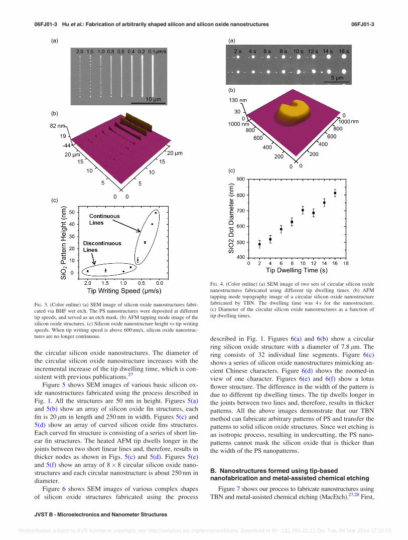
the circular silicon oxide nanostructures. The diameter of
the circular silicon oxide nanostructure increases with the
incremental increase of the tip dwelling time, which is con-
sistent with previous publications.27
Figure 5 shows SEM images of various basic silicon ox-
ide nanostructures fabricated using the process described in
Fig. 1. All the structures are 50 nm in height. Figures 5(a)
and 5(b) show an array of silicon oxide fin structures, each
fin is 20 lm in length and 250 nm in width. Figures 5(c) and
5(d) show an array of curved silicon oxide fins structures.
Each curved fin structure is consisting of a series of short lin-
ear fin structures. The heated AFM tip dwells longer in the
joints between two short linear lines and, therefore, results in
thicker nodes as shown in Figs. 5(c) and 5(d). Figures 5(e)
and 5(f) show an array of 8� 8 circular silicon oxide nano-
structures and each circular nanostructure is about 250 nm in
diameter.
Figure 6 shows SEM images of various complex shapes
of silicon oxide structures fabricated using the process
described in Fig. 1. Figures 6(a) and 6(b) show a circular
ring silicon oxide structure with a diameter of 7.8 lm. The
ring consists of 32 individual line segments. Figure 6(c)
shows a series of silicon oxide nanostructures mimicking an-
cient Chinese characters. Figure 6(d) shows the zoomed-in
view of one character. Figures 6(e) and 6(f) show a lotus
flower structure. The difference in the width of the pattern is
due to different tip dwelling times. The tip dwells longer in
the joints between two lines and, therefore, results in thicker
patterns. All the above images demonstrate that our TBN
method can fabricate arbitrary patterns of PS and transfer the
patterns to solid silicon oxide structures. Since wet etching is
an isotropic process, resulting in undercutting, the PS nano-
patterns cannot mask the silicon oxide that is thicker than
the width of the PS nanopatterns.
B. Nanostructures formed using tip-basednanofabrication and metal-assisted chemical etching
Figure 7 shows our process to fabricate nanostructures using
TBN and metal-assisted chemical etching (MacEtch).27,28 First,
FIG. 3. (Color online) (a) SEM image of silicon oxide nanostructures fabri-
cated via BHF wet etch. The PS nanostructures were deposited at different
tip speeds, and served as an etch mask. (b) AFM tapping mode image of the
silicon oxide structures. (c) Silicon oxide nanostructure height vs tip writing
speeds. When tip writing speed is above 600 nm/s, silicon oxide nanostruc-
tures are no longer continuous.
FIG. 4. (Color online) (a) SEM image of two sets of circular silicon oxide
nanostructures fabricated using different tip dwelling times. (b) AFM
tapping mode topography image of a circular silicon oxide nanostructure
fabricated by TBN. The dwelling time was 4 s for the nanostructure.
(c) Diameter of the circular silicon oxide nanostructures as a function of
tip dwelling times.
06FJ01-3 Hu et al.: Fabrication of arbitrarily shaped silicon and silicon oxide nanostructures 06FJ01-3
JVST B - Microelectronics and Nanometer Structures
Redistribution subject to AVS license or copyright; see http://scitation.aip.org/termsconditions. Download to IP: 132.250.22.11 On: Tue, 04 Mar 2014 17:32:05
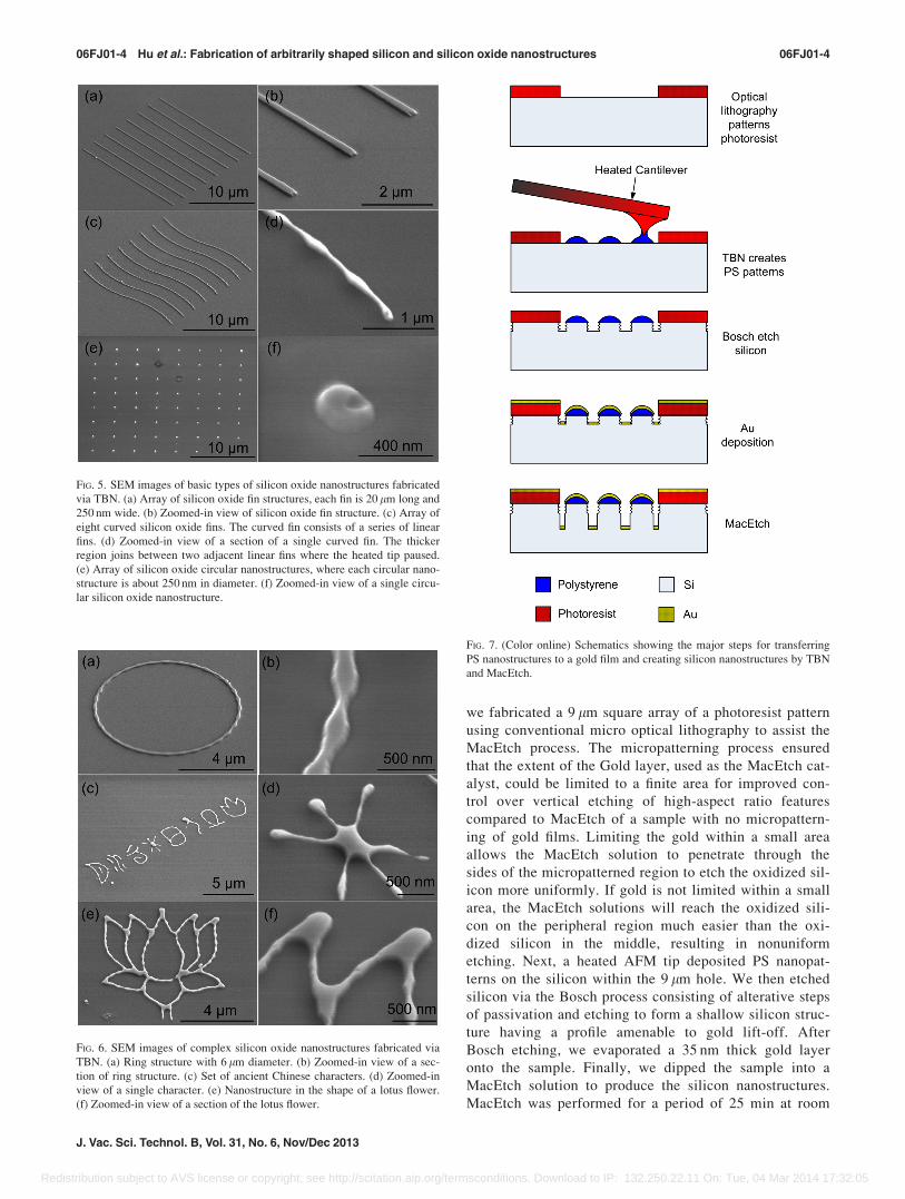
we fabricated a 9 lm square array of a photoresist pattern
using conventional micro optical lithography to assist the
MacEtch process. The micropatterning process ensured
that the extent of the Gold layer, used as the MacEtch cat-
alyst, could be limited to a finite area for improved con-
trol over vertical etching of high-aspect ratio features
compared to MacEtch of a sample with no micropattern-
ing of gold films. Limiting the gold within a small area
allows the MacEtch solution to penetrate through the
sides of the micropatterned region to etch the oxidized sil-
icon more uniformly. If gold is not limited within a small
area, the MacEtch solutions will reach the oxidized sili-
con on the peripheral region much easier than the oxi-
dized silicon in the middle, resulting in nonuniform
etching. Next, a heated AFM tip deposited PS nanopat-
terns on the silicon within the 9 lm hole. We then etched
silicon via the Bosch process consisting of alterative steps
of passivation and etching to form a shallow silicon struc-
ture having a profile amenable to gold lift-off. After
Bosch etching, we evaporated a 35 nm thick gold layer
onto the sample. Finally, we dipped the sample into a
MacEtch solution to produce the silicon nanostructures.
MacEtch was performed for a period of 25 min at room
FIG. 5. SEM images of basic types of silicon oxide nanostructures fabricated
via TBN. (a) Array of silicon oxide fin structures, each fin is 20 lm long and
250 nm wide. (b) Zoomed-in view of silicon oxide fin structure. (c) Array of
eight curved silicon oxide fins. The curved fin consists of a series of linear
fins. (d) Zoomed-in view of a section of a single curved fin. The thicker
region joins between two adjacent linear fins where the heated tip paused.
(e) Array of silicon oxide circular nanostructures, where each circular nano-
structure is about 250 nm in diameter. (f) Zoomed-in view of a single circu-
lar silicon oxide nanostructure.
FIG. 6. SEM images of complex silicon oxide nanostructures fabricated via
TBN. (a) Ring structure with 6 lm diameter. (b) Zoomed-in view of a sec-
tion of ring structure. (c) Set of ancient Chinese characters. (d) Zoomed-in
view of a single character. (e) Nanostructure in the shape of a lotus flower.
(f) Zoomed-in view of a section of the lotus flower.
FIG. 7. (Color online) Schematics showing the major steps for transferring
PS nanostructures to a gold film and creating silicon nanostructures by TBN
and MacEtch.
06FJ01-4 Hu et al.: Fabrication of arbitrarily shaped silicon and silicon oxide nanostructures 06FJ01-4
J. Vac. Sci. Technol. B, Vol. 31, No. 6, Nov/Dec 2013
Redistribution subject to AVS license or copyright; see http://scitation.aip.org/termsconditions. Download to IP: 132.250.22.11 On: Tue, 04 Mar 2014 17:32:05
temperature in a solution of HF, hydrogen peroxide
(H2O2), and ethanol (EtOH), with a volumetric ratio of
1:2:2, respectively (molar concentration of [HF]¼ 5.75 M,
[H2O2]¼ 3.88 M, [EtOH]¼ 6.86 M).
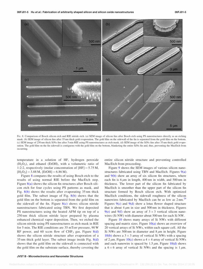
Figure 8 compares the results of using Bosch etch to the
results of using normal RIE before the MacEtch step.
Figure 8(a) shows the silicon fin structures after Bosch sili-
con etch for four cycles using PS patterns as mask, and
Fig. 8(b) shows the results after evaporating 35 nm thick
gold film. The subset image of Fig. 8(b) shows that the
gold film on the bottom is separated from the gold film on
the sidewall of the fin. Figure 8(c) shows silicon nitride
nanostructures fabricated using TBN. We first deposited
PS nanostructures using the heated AFM tip on top of a
250 nm thick silicon nitride layer prepared by plasma
enhanced chemical vapor deposition. Then, we etched the
silicon nitride using PS nanostructures as etch mask in RIE
for 5 min. The RIE conditions are 35 mTorr pressure, 90 W
RF power, and 60 sccm flow of CHF3 gas. Figure 8(d)
shows the silicon nitride structure after evaporation of a
35 nm thick gold layer. The subset image inside Fig. 8(d)
shows that the gold film on the sidewall is connected with
the gold film on the substrate surface, thereby covering the
entire silicon nitride structure and preventing controlled
MacEtch from proceeding.
Figure 9 shows the SEM images of various silicon nano-
structures fabricated using TBN and MacEtch. Figures 9(a)
and 9(b) show an array of six silicon fin structures, where
each fin is 6 lm in length, 400 nm in width, and 500 nm in
thickness. The lower part of the silicon fin fabricated by
MacEtch is smoother than the upper part of the silicon fin
structure formed by Bosch silicon etch. With optimized
MacEtch conditions, the sidewall roughness of the silicon
nanowires fabricated by MacEtch can be as low as 2 nm.29
Figures 9(c) and 9(d) show a lotus flower shaped structure
that is about 4 lm in size and 500 nm in thickness. Figures
9(e) and 9(f) show an array of 3� 3 vertical silicon nano-
wires (Si NW) with diameter about 500 nm for each Si NW.
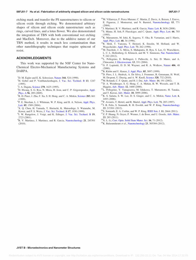
Figure 10 shows many arrays of Si NWs with different
spacing and matrix sizes. Figure 10(a) shows an overview of
20 vertical arrays of Si NWs, within each square cell. All the
Si NWs are 500 nm in diameter and 8 lm in height. Figure
10(b) shows a 3� 3 array of vertical Si NWs with a spacing
of 2 lm. Figure 10(c) shows a 4� 4 array of vertical Si NWs
and each nanowire is spaced by 1.5 lm. Figure 10(d) shows
a 6� 6 array of vertical Si NWs and the spacing is 1 lm.
FIG. 8. Comparison of Bosch silicon etch and RIE nitride etch. (a) SEM image of silicon fins after Bosch etch using PS nanostructures directly as an etching
mask. (b) SEM image of silicon fins after 35 nm thick gold evaporation. The gold film on the sidewall of the fin is separated from the gold film on the bottom.
(c) SEM image of 250 nm thick SiNx fins after 5 min RIE using PS nanostructures as etch mask. (d) SEM image of the SiNx fins after 35 nm thick gold evapo-
ration. The gold film on the fin sidewall is contiguous with the gold film on the bottom, blanketing the entire SiNx fin and, thus, preventing the MacEtch from
occurring.
06FJ01-5 Hu et al.: Fabrication of arbitrarily shaped silicon and silicon oxide nanostructures 06FJ01-5
JVST B - Microelectronics and Nanometer Structures
Redistribution subject to AVS license or copyright; see http://scitation.aip.org/termsconditions. Download to IP: 132.250.22.11 On: Tue, 04 Mar 2014 17:32:05
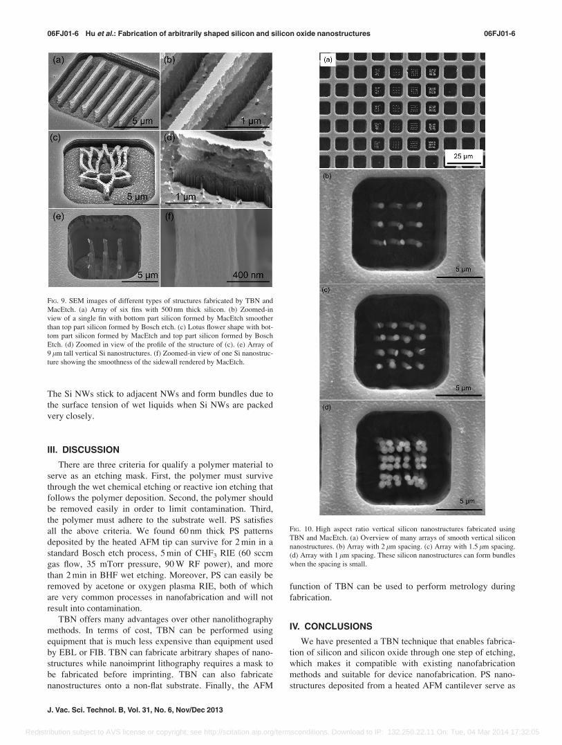
The Si NWs stick to adjacent NWs and form bundles due to
the surface tension of wet liquids when Si NWs are packed
very closely.
III. DISCUSSION
There are three criteria for qualify a polymer material to
serve as an etching mask. First, the polymer must survive
through the wet chemical etching or reactive ion etching that
follows the polymer deposition. Second, the polymer should
be removed easily in order to limit contamination. Third,
the polymer must adhere to the substrate well. PS satisfies
all the above criteria. We found 60 nm thick PS patterns
deposited by the heated AFM tip can survive for 2 min in a
standard Bosch etch process, 5 min of CHF3 RIE (60 sccm
gas flow, 35 mTorr pressure, 90 W RF power), and more
than 2 min in BHF wet etching. Moreover, PS can easily be
removed by acetone or oxygen plasma RIE, both of which
are very common processes in nanofabrication and will not
result into contamination.
TBN offers many advantages over other nanolithography
methods. In terms of cost, TBN can be performed using
equipment that is much less expensive than equipment used
by EBL or FIB. TBN can fabricate arbitrary shapes of nano-
structures while nanoimprint lithography requires a mask to
be fabricated before imprinting. TBN can also fabricate
nanostructures onto a non-flat substrate. Finally, the AFM
function of TBN can be used to perform metrology during
fabrication.
IV. CONCLUSIONS
We have presented a TBN technique that enables fabrica-
tion of silicon and silicon oxide through one step of etching,
which makes it compatible with existing nanofabrication
methods and suitable for device nanofabrication. PS nano-
structures deposited from a heated AFM cantilever serve as
FIG. 9. SEM images of different types of structures fabricated by TBN and
MacEtch. (a) Array of six fins with 500 nm thick silicon. (b) Zoomed-in
view of a single fin with bottom part silicon formed by MacEtch smoother
than top part silicon formed by Bosch etch. (c) Lotus flower shape with bot-
tom part silicon formed by MacEtch and top part silicon formed by Bosch
Etch. (d) Zoomed in view of the profile of the structure of (c). (e) Array of
9 lm tall vertical Si nanostructures. (f) Zoomed-in view of one Si nanostruc-
ture showing the smoothness of the sidewall rendered by MacEtch.
FIG. 10. High aspect ratio vertical silicon nanostructures fabricated using
TBN and MacEtch. (a) Overview of many arrays of smooth vertical silicon
nanostructures. (b) Array with 2 lm spacing. (c) Array with 1.5 lm spacing.
(d) Array with 1 lm spacing. These silicon nanostructures can form bundles
when the spacing is small.
06FJ01-6 Hu et al.: Fabrication of arbitrarily shaped silicon and silicon oxide nanostructures 06FJ01-6
J. Vac. Sci. Technol. B, Vol. 31, No. 6, Nov/Dec 2013
Redistribution subject to AVS license or copyright; see http://scitation.aip.org/termsconditions. Download to IP: 132.250.22.11 On: Tue, 04 Mar 2014 17:32:05
etching mask and transfer the PS nanostructures to silicon or
silicon oxide through etching. We demonstrated arbitrary
shapes of silicon and silicon oxide nanostructure such as
rings, curved lines, and a lotus flower. We also demonstrated
the integration of TBN with both conventional wet etching
and MacEtch. Moreover, due to the additive nature of our
TBN method, it results in much less contamination than
other nanolithography techniques that require spincoat of
resist.
ACKNOWLEDGMENTS
This work was supported by the NSF Center for Nano-
Chemical Electro-Mechanical Manufacturing Systems and
DARPA.
1D. M. Eigler and E. K. Schweizer, Nature 344, 524 (1990).2H. Gobel and P. Vonblanckenhagen, J. Vac. Sci. Technol. B 13, 1247
(1995).3J. A. Dagata, Science 270, 1625 (1995).4D. Hwang, S. G. Ryu, N. Misra, H. Jeon, and C. P. Grigoropoulos, Appl.
Phys. A 96, 289 (2009).5R. D. Piner, J. Zhu, F. Xu, S. H. Hong, and C. A. Mirkin, Science 283, 661
(1999).6P. E. Sheehan, L. J. Whitman, W. P. King, and B. A. Nelson, Appl. Phys.
Lett. 85, 1589 (2004).7X. Q. Chen, H. Yamada, T. Horiuchi, K. Matsushige, S. Watanabe, M.
Kawai, and P. S. Weiss, J. Vac. Sci. Technol. B 17, 1930 (1999).8I. W. Rangelow, J. Voigt, and K. Edinger, J. Vac. Sci. Technol. B 19,
2723 (2001).9R. V. Martinez, J. Martinez, and R. Garcia, Nanotechnology 21, 245301
(2010).
10M. Villarroya, F. Perez-Murano, C. Martin, Z. Davis, A. Boisen, J. Esteve,
E. Figueras, J. Montserrat, and N. Barniol, Nanotechnology 15, 771
(2004).11J. Martinez, R. V. Martinez, and R. Garcia, Nano. Lett. 8, 3636 (2008).12S. Minne, H. Soh, P. Flueckiger, and C. Quate, Appl. Phys. Lett. 66, 703
(1995).13K. Matsumoto, M. Ishii, K. Segawa, Y. Oka, B. Vartanian, and J. Harris,
Appl. Phys. Lett. 68, 34 (1996).14R. Held, T. Vancura, T. Heinzel, K. Ensslin, M. Holland, and W.
Wegscheider, Appl. Phys. Lett. 73, 262 (1998).15M. Fuechsle, J. A. Miwa, S. Mahapatra, H. Ryu, S. Lee, O. Warschkow,
L. C. L. Hollenberg, G. Klimeck, and M. Y. Simmons, Nat. Nanotechnol.
7, 242 (2012).16L. Pellegrino, E. Bellingeri, I. Pallecchi, A. Siri, D. Marre, and A.
Chincarini, J. Electroceram. 13, 331 (2004).17G. P. Lopinski, D. D. M. Wayner, and R. A. Wolkow, Nature 406, 48
(2000).18B. Klehn and U. Kunze, J. Appl. Phys. 85, 3897 (1999).19D. Pires, J. L. Hedrick, A. De Silva, J. Frommer, B. Gotsmann, H. Wolf,
M. Despont, U. Duerig, and A. W. Knoll, Science 328, 732 (2010).20M. Rolandi, C. F. Quate, and H. J. Dai, Adv. Mater. 14, 191 (2002).21D. A. Weinberger, S. G. Hong, C. A. Mirkin, B. W. Wessels, and T. B.
Higgins, Adv. Mater. 12, 1600 (2000).22L. Pellegrino, Y. Yanagisawa, M. Ishikawa, T. Matsumoto, H. Tanaka,
and T. Kawai, Adv. Mater. 18, 3099 (2006).23K. S. Salaita, S. W. Lee, D. S. Ginger, and C. A. Mirkin, Nano. Lett. 6,
2493 (2006).24P. Avouris, T. Hertel, and R. Martel, Appl. Phys. Lett. 71, 285 (1997).25J. R. Felts, S. Somnath, R. H. Ewoldt, and W. P. King, Nanotechnology
23, 215301 (2012).26S. Somnath, E. A. Corbin, and W. P. King, IEEE Sen. J. 11, 2664 (2011).27Z. P. Huang, N. Geyer, P. Werner, J. de Boor, and U. Gosele, Adv. Mater.
23, 285 (2011).28X. L. Li, Curr. Opin. Solid State Mater. Sci. 16, 71 (2012).29K. Balasundaram et al., Nanotechnology 23, 305304 (2012).
06FJ01-7 Hu et al.: Fabrication of arbitrarily shaped silicon and silicon oxide nanostructures 06FJ01-7
JVST B - Microelectronics and Nanometer Structures
Redistribution subject to AVS license or copyright; see http://scitation.aip.org/termsconditions. Download to IP: 132.250.22.11 On: Tue, 04 Mar 2014 17:32:05