Fabrication, Characterization, and Modelling of Self-Assembled ...
264
Fabrication, Characterization, and Modelling of Self-Assembled Silicon Nanostructure Vacuum Field Emission Devices By Mohammad Rezaul Bari BSc (EEE), Bangladesh University of Engineering and Technology (1989) MSEE, Louisiana State University (1995) Member, IEEE A thesis presented for the degree of Doctor of Philosophy in Electrical and Electronic Engineering at the University of Canterbury Christchurch, New Zealand December 2011
Transcript of Fabrication, Characterization, and Modelling of Self-Assembled ...
Fabrication, Characterization, and Modelling of
Self-Assembled Silicon Nanostructure
Vacuum Field Emission Devices
By
Mohammad Rezaul Bari
BSc (EEE), Bangladesh University of Engineering and Technology (1989)
MSEE, Louisiana State University (1995)
Member, IEEE
A thesis presented for the degree of
Doctor of Philosophy
in
Electrical and Electronic Engineering
at the
University of Canterbury
Christchurch, New Zealand
December 2011


In loving memory of my father
Mohammad Osman Gani
(17 January 1941 – 5 September 1999)


5
Abstract
The foundation of vacuum nanoelectronics was laid as early as in 1961 when Kenneth
Shoulders proposed the development of vertical field-emission micro-triodes. After
years of conspicuous stagnancy in the field much interest has reemerged for the
vacuum nanoelectronics in recent years. Electron field emission under high electric
field from conventional and exotic nanoemitters, which have now been made possible
with the use of modern day technology, has been the driving force behind this renewal
of interest in vacuum nanoelectronics. In the research reported in this thesis self-
assembled silicon nanostructures were studied as a potential source of field emission
for vacuum nanoelectronic device applications.
Whiskerlike protruding silicon nanostructures were grown on untreated n- and p-
type silicon surfaces using electron-beam annealing under high vacuum. The electrical
transport characteristics of the silicon nanostructures were investigated using
conductive atomic force microscopy (C-AFM). Higher electrical conductivities for the
nanostructured surface compared to that for the surrounding planar silicon substrate
region were observed. Non-ideal diode behaviour with high ideality factors were
reported for the individual nanostructure-AFM tip Schottky nanocontacts. This
demonstration, indicative of the presence of a significant field emission component in
the analysed current transport phenomena was also detailed. Field emission from these
nanostructures was demonstrated qualitatively in a lift-mode interleave C-AFM study.
A technique to fabricate integrated field emission diodes using silicon
nanostructures in a CMOS process technology was developed. The process
incorporated the nanostructure growth phase at the closing steps in the process flow.
Turn-on voltages as low as ~ 0.6 V were reported for these devices, which make them
good candidates for incorporation into standard CMOS circuit applications.
Reproducible I-V characteristics exhibited by these fabricated devices were
further studied and field emission parameters were extracted. A new consistent and
reliable method to extract field emission parameters such as effective barrier height,
field conversion factor, and total emitting area at the onset of the field emission regime
was developed and is reported herein. The parameter extraction method developed
used a unified electron emission approach in the transition region of the device
6
operation. The existence of an electron-supply limited current saturation region at very
high electric field was also confirmed.
Both the C-AFM and the device characterization studies were modelled and
simulated using the finite element method in COMSOL Multiphysics. The
experimental results – the field developed at various operating environments – are
explained in relation to these finite element analyses. Field enhancements at the
atomically sharp nanostructure apexes as suggested in the experimental studies were
confirmed. The nanostructure tip radius effect and sensitivity to small nanostructure
height variation were investigated and mathematical relations for the nanostructure
regime of our interest were established. A technique to optimize the cathode-opening
area was also demonstrated.
Suggestions related to further research on field emission from silicon
nanostructures, optimization of the field emission device fabrication process, and
fabrication of field emission triodes are elaborated in the final chapter of this thesis.
The experimental, modelling, and simulation works of this thesis indicate that
silicon field emission devices could be integrated into the existing CMOS process
technology. This integration would offer advantages from both the worlds of vacuum
and solid-sate nanoelectronics – fast ballistic electron transport, temperature
insensitivity, radiation hardness, high packing density, mature technological backing,
and economies of scale among other features.

7
Preface
This dissertation embodies the research undertaken by the author at the Department of
Electrical and Computer Engineering at the University of Canterbury between
September 2008 and November 2011. The experimental works were carried out in the
department’s Nanofabrication Laboratory and at the laboratory of the GNS Science in
Wellington, New Zealand. The funding for the work was provided by the MacDiarmid
Institute for Advanced Materials and Nanotechnology through a Doctoral Scholarship.
Some aspects of the work described herein have been published and presented as
follows:
M. R. Bari, R. J. Blaikie, F. Fang, and A. Markwitz, “Conductive atomic force
microscopy study of self-assembled silicon nanostructures,” Journal of Vacuum
Science & Technology B, Vol. 27, No. 6, pp. 3051-3054, 2009.
M. R. Bari, S. P. Lansley, R. J. Blaikie, F. Fang, A. Markwitz, “Fabrication and
characterization of integrated field emission diodes using self-assembled-silicon-
nanostructure cathodes,” Proceedings of the Conference on Optoelectronic and
Microelectronic Materials and Devices (COMMAD), Canberra, Australia, 12-15
December 2010, IEEE Press (IEEE catalog number CFP10763-PRT, ISBN 978-1-
4244-7332-8), pp. 227-228. (Oral presentation)
M. R. Bari, R. J. Blaikie, S. P. Lansley, F. Fang, D. Carder, and A. Markwitz,
“Fowler-Nordheim Current Saturation in Integrated Field-Emission Diode,” Abstracts
of the Fifth International Conference on Advanced Materials and Nanotechnology
(AMN-5), Wellington, New Zealand, 7-11 February 2011. (Poster presentation)

8

9
Acknowledgements
First and the foremost I would like to thank my supervisor Professor Richard Blaikie.
Richard introduced me to the amazing world of nanotechnology and encouraged,
supported and guided me all along this research. Richard’s encouragement had started
even before I got my admission at the University of Canterbury. When I contemplated
pursuing a PhD, and when I was searching for opportunities world over, it was
Richard who provided me the most positive feedback from this faraway place called
New Zealand. I never looked back since then, and I undertook the challenge, which
has been made easy during the last three years with Richard’s dynamic humane
leadership and effective technical guidance. Every time I have interacted with him, I
have learned of innovative ideas, and arrived at feasible and simple solutions to
complex problems, which contributed immensely to the completion of this thesis
within a reasonable time. His advices, comments, and recommendations have had a
substantial influence on the quality of this dissertation. Richard has been a true mentor,
a firm guide, and a caring supervisor all through this testing time. Thanks again,
Richard.
I appreciate the guidance and invaluable support provided by Dr. Andreas
Markwitz, Principal Scientist (Nanotechnology) of GNS Science, New Zealand. I
would like to thank Andreas sincerely for agreeing to be my co-supervisor for the
research work, which took me to the Crown Research Institute’s Wellington facility
multiple times. Ion implantation and electron beam annealing, the two key process
steps, were carried out in the GNS laboratory.
I would like to express particular gratitude to Dr. Stuart Lansley, initially post-
doctoral fellow in the Department of Physics and at present lecturer in the Department
of Electrical and Computer Engineering, for his expert advice on the continuing
research during our countless weekly meetings with Richard and beyond.
The research embodied in this thesis has been carried out primarily in the
Nanofabrication Laboratory at the Department of Electrical and Computer Engineering
at the University of Canterbury. Financial provision was provided by the MacDiarmid
Institute for Advanced Materials and Nanotechnology through a Doctoral Scholarship.
These are the two key supports, facilities and funding, which made this thesis possible.
I am grateful to Gary Turner and Helen Devereux for they provided the required
training and advice on various facilities and resources at the Nanofabrication

10
Laboratory. Thanks also to Dr. Volker Nock who was around in the laboratory most of
the time and who eagerly extended his help and advice when going got tough.
I would like to thank Dr. Vivian Fang and Dr. Damian Carder, Scientist:
Nanoelectronics Research, GNS Science, New Zealand, for their help with the electron
beam annealing and the ion implantation, Gary Turner with the Scanning Electron
Microscopy, Dr. Lakshman De Silva with the ellipsometry, and Pieter Kikstra with the
computer hardware and software.
Special thanks also go to my colleagues and mentors in the lab and in the office:
Ciaran Moore, Mikkel Schøler, Prateek Mehrotra, Jannah Ibrahim, Lynn Murray,
Arunava ‘Steve’ Banerjee, and Shazlina Johari. I also thank the local small, yet
vibrant, Bangladeshi community for making our stay in Christchurch a pleasant one.
A series of events that occurred during the time of the research was unique and
calls for a special mention. That was the great September 2010 earthquake and the
subsequent big aftershocks of February and June that left Christchurch a devastated
city. I would like to thank everyone in Christchurch, especially my supervisor, co-
supervisor, other teaching members, colleagues, friends and family, the department,
and the university authority for the support and care provided during those difficult
days of violent earthquakes and aftershocks. Without their active and efficient
handling of the matters related to the earthquake and associated issues, this thesis
would have remained incomplete.
I am particularly indebted to the endless love, unconditional sacrifice and
immense fortitude of my wife Sultana, who at times had to carry the burden of the
family alone, and appreciate the understanding of our daughter Nadia and our son
Wasiq, who would often miss their dad’s care over the course of this research. I wish
to thank my mother Raihanul Jannat, mother- and father-in-law Josna Ara and
Mohammad Abul Kashem, and my sisters Afroza and Arifa for their love and
motivation that facilitated my going the distance. Persistent support, moral
encouragement and infinite patience from my family members here and abroad have
enabled me to complete this thesis; indeed, I could not have done this without them
being around.
Today, I fondly remember my father, who always wanted to see his only son as a
doctorate. He is no more with us, but his wish has been a constant inspiration that has
finally led me to this day; a step closer in completing the requirements of a doctorate
degree. May God bless him and us everybody.
11
Contents
Abstract 5
Preface 7
Acknowledgements 9
Contents 11
List of Figures 17
List of Tables 29
Chapters
1 Introduction 31
1.1 Vacuum Microelectronics 31
1.2 Work Function, Fermi Level, and Electron Emission from Metal 36
1.2.1 Thermionic Emission 40
1.2.2 Photoelectric Emission 41
1.2.3 Secondary Emission 42
1.2.4 Schottky Emission 42
1.2.5 Field Emission 43
1.3 Applications of Vacuum Field Emission and Motivation 45
1.4 Objectives of the Work 49
1.5 Dissertation Outline 49
2 Background – Field Emission,
Field Emitters, and Field-Emission Devices 53
2.1 Electron Emission from Metals under the Influence of Electric Fields 54
2.1.1 Tunnelling of Electrons through Narrow Potential Barrier 54
2.1.2 Image Effect and Schottky Barrier Lowering 57
2.1.3 Quantum Mechanical Tunnelling
through Single Rectangular Potential Barrier 59
2.1.4 Tunnelling through Triangular Potential Barrier 60
2.1.5 Schottky Emission 61
2.1.6 Extended Schottky Emission and the Transition Region 62
2.2 Field Emission from Semiconductors 63
2.2.1 Supply of Electrons and the Simplest
Model of Electron Emission from Semiconductors 64

12
2.2.2 Field Penetration Effect 66
2.2.2 Image Charge Effect 68
2.3 Field Enhancement and Emitter Shape 68
2.3.1 Concentric Electrodes Model 69
2.3.2 Rounded Whisker Model 70
2.3.3 Simulation of the Emitting Structures 71
2.3.4 General Comments on Emitter Shapes 73
2.4 Fabrication of Field Emitters 73
2.4.1 Spindt Cathodes 74
2.4.2 Silicon Etched Structures 75
2.4.3 VLS Method 77
2.4.4 Laser Ablation VLS Method 79
2.4.5 SLS Synthesis 80
2.4.5 Carbon Nanotubes 81
2.5 The GNS Self-assembled Silicon Nanostructures 82
2.5.1 Growth Mechanism 82
2.5.1.1 Oxide Desorption, Void Formation
and Surface Roughening 83
2.5.1.2 Epitaxial Nanocrystal Growth 84
2.5.2 Role of Electron Beam in Nanostructure Growth 85
2.6 From Field Emitters to Field Emission Devices 86
2.6.1 Silicon Field Emission Diodes 87
2.6.2 Carbon Nanotubes Field Emission Diodes 89
2.7 Summary 91
3 Process and Characterization – Methods and Tools 93
3.1 Oxidation 95
3.1.1 Oxidation Apparatus 97
3.1.2 Oxide Thickness Measurement 98
3.2 Optical Lithography 99
3.2.1 Masks 101
3.2.2 Photoresists 102
3.2.3 Exposure Techniques and Tools 103
3.3 Etching 105
13
3.3.1 Wet Etching 106
3.3.2 Dry Etching 108
3.4 Ion Implantation 112
3.4.1 Ion Implantation System 112
3.4.2 Implantation Dose and Impurity Concentration 114
3.4.3 Advantages of Ion Implantation 115
3.4.4 Implantation Damage 115
3.4.5 Annealing 116
3.5 Metallization 117
3.6 Electron Beam Annealing 119
3.7 Atomic Force Microscopy 121
3.7.1 AFM Basic Principle 122
3.7.2 AFM Modes of Operation 123
3.7.3 Other Aspects of AFM 126
3.8 Other Experimental Techniques and Apparatuses 128
3.8.1 Surface Profilometry 128
3.8.2 Ellipsometry 129
3.8.3 Scanning Electron Microscopy 130
3.8.4 I-V Characterization 130
3.9 Summary 131
4 Conductive AFM Studies of
Self-Assembled Silicon Nanostructures 133
4.1 Introduction 133
4.2 The Conductive Atomic Force Microscopy 134
4.2.1 Conductive Probes 135
4.2.2 The TUNA Application Module 136
4.2.3 Interleave Scanning and C-AFM in Lift-mode 138
4.3 C-AFM Experimental Details 140
4.3.1 Sample Preparation 140
4.3.2 Measurements 141
4.3.3 Precautions 142
4.4 C-AFM Results and Discussion 142
4.4.1 Standard Conductive Scan Results 142
14
4.4.2 I-V Spectroscopy Results 147
4.4.3 Theoretical Analysis of the I-V Spectroscopy Results 148
4.4.4 Interleave Lift-mode Conductive AFM Results 153
4.5 Summary 155
5 Fabrication of an Integrated Field-Emission Diode 157
5.1 Introduction 158
5.2 Mask Fabrication for Optical Lithography 159
5.2.1 Mask Layout 160
5.2.2 Transfer of Mask Layout to a Photomask 162
5.2.3 Mask Photoresist Development 163
5.2.4 Chrome Etch 163
5.2.5 Stripping Resist from the Mask Plate 164
5.2.6 Precautions 165
5.3 Process Integration 165
5.3.1 Oxidation 166
5.3.2 Photolithography – Mask 1: Cathode contact 166
5.3.3 SiO2 Etch 168
5.3.4 Ion Implantation 169
5.3.5 Metal Deposition 170
5.3.6 Photolithography – Mask 2: Metal 171
5.3.7 Metal Etch 172
5.3.8 Photolithography – Mask 3: Nanostructure area 174
5.3.9 Metal Etch 175
5.3.10 SiO2 Etch 175
5.3.11 Electron Beam Anneal 177
5.4 Process Integration Issues 179
5.5 Summary 181
6 Characterization of the Integrated Field-Emission Diode 183
6.1 Experimental Setup 184
6.2 Origin of Significant Current 186
6.3 Observation of Schottky Emission at Low Field
and Fowler-Nordheim Emission at High Field 189
15
6.4 Extraction of Parameters - Theory and Results 192
6.4.1 Theory for Extraction of Parameters 192
6.4.2 Results from Parameter Extraction 195
6.5 Deviation of Fowler-Nordheim Behaviour at High Field 200
6.6 Summary 201
7 Modelling and Simulation of Field Enhancement 203
7.1 Electrostatics, the Finite Element Method, and COMSOL 204
7.1.1 Poisson and Laplace Equations 204
7.1.2 Outline of the Finite Element Method 205
7.1.3 COMSOL Multiphysics for
the Calculation of Electrostatic Field 206
7.2 Validation of the Simulation 208
7.2.1 Hemisphere on a Plane: Two-dimensional (2D) Simulation 208
7.2.2 Hemisphere on a Plane: Axisymmetric Simulation 211
7.2.3 Electric Field around Rounded Whisker 215
7.2.4 Field Enhancement in Sharp Emitters 217
7.3 Field Enhancement: AFM Probes and GNS Nanostructures 219
7.4 Field Enhancement in the Fabricated Devices 223
7.4.1 Tip Radius Effect 224
7.4.2 Sensitivity to Small Height Variation 225
7.4.3 Cathode-Opening Area Optimization 226
7.5 Conclusions 227
8 Conclusions and Future Work 229
8.1 Summary of Results 229
8.2 Recommendations for Future Work 232
8.2.1 Further investigation of individual nanostructures 233
8.2.2 Fabrication of optimized field emission diodes 233
8.2.3 Fabrication of field emission triode
using silicon nanostructures 235
8.3 Final Comments 239

16
Appendixes 241
A. Selected Fundamental Physical Constants 241
B. Electron Work Function of Selected Elements 242
C. Properties of Silicon 243
D. Properties of SiO2 244
E. Definition of Ion Implantation Terms 245
References 247
17
List of Figures
1.1 Top view and side view of tunnel effect vacuum triode. 33
1.2 Thin-film field emission cathode fabricated by C. A. Spindt. 34
1.3 (a) A scanning electron micrograph and (b) cross-section view of a
planar silicon field emitter array field effect transistor. 35
1.4 The energy of a “free” electron inside the metal is lower than the
vacuum outside by an amount of energy called the work function.
Redrawn with relevant changes. 37
1.5 Electron energy band diagram for Aluminium at 0 K. Work function of
Al is 4.28 eV. 38
1.6 (a) The density of states (E) vs. E in the energy band. (b) The Fermi-
Dirac distribution at 0 K. (c) Electron concentration per unit energy nE at
0 K. (d) Electron energy band diagram at 0 K, no electrons are available
above EF. 39
1.7 (a) The density of states (E) vs. E in the energy band. (b) The Fermi-
Dirac distribution at a high temperature, T. (c) Electron concentration
per unit energy nE at T. (d) Electron energy band diagram at T, electrons
are available above EF, even up to EF + . 40
1.8 Schematic of thermionic emission. At high temperature there are
electrons occupying energy levels at or above the vacuum level that take
part in the thermionic emission. 41
1.9 Schematic representation of photoelectric emission. h is supplied by
the photons. 42
1.10 Schematic representation of Schottky emission. Applied field F bended
the vacuum level and lowered the original potential barrier by an
amount . 43
1.11 Schematic representation of electron field emission at room temperature.
Applied high electric field F bended the vacuum level so much so that
electrons near Fermi level tunnel through the thin barrier. 44
1.12 Schematic representation of electron field emission at absolute zero.
Field emission is still possible under high electric field as electrons near
Fermi level can tunnel through the thin barrier. 44

18
1.13 Vertical vacuum diode and triode configurations. 45
1.14 Cross-sectional diagram of a typical field-emission display shows the
sharp emitters and the associated structures. 46
1.15 Transit time t for d = 0.5 m as function of applied voltage V. 47
2.1 Triangular potential barrier under electric field without considering
image charge effect at absolute zero temperature. 55
2.2 Minimum field requirements (theoretical) for field emissions from
common metals are plotted with respect to their work functions. Values
for work function considered are the minimum values taken from among
values of different planes for a given metal. 56
2.3 The ‘image charge’ theorem. The effect of a plane conductor on the
static field due to a charged particle is equivalent to a second, oppositely
charged, particle in the mirror image position. 57
2.4 Schottky “barrier lowering” from the image charge effect. The applied
field is 6x10⁷ V/cm. 58
2.5 Electron emission from metal surface can at the simplest form be
modelled approximately as a quantum mechanical problem of an
electron with EF kinetic energy encountering a rectangular barrier of
height EF + and width a. 59
2.6 Schematic representation of electron emission in the transition region.
Electrons from both above and below the top of the potential barrier
contribute to the emission current. 63
2.7 (From left) Schematic band diagram, density of states, Fermi-Dirac
distribution function, and the carrier concentrations for (a) intrinsic, (b)
n-type, and (c) p-type semiconductors at thermal equilibrium at T, where
T 0 K. ND, NA are the donor and acceptor impurities concentrations. 65
2.8 Schematic of the simplest model of field emission from an n-type
semiconductor. The model is same for p-type semiconductor too.
Electrons at the bottom of the conduction band encounter a potential
barrier of height and width a at field F1, while for electrons at the top
of the valence band the barrier height is + Eg. For the tunneling from
top of the valence band to be significant at the same barrier width a, a
higher field F2 is required.
66
19
2.9 Field emission from the conduction band of an n-type semiconductor
with field penetration. The conduction band has bent but (a) has not
dipped below the Fermi level, and (b) has dipped below the Fermi level
near the semiconductor surface. 67
2.10 Concentric emitter and collector model. When rd , rVF / . 69
2.11 Various shapes of sharp field emitters: (a) rounded whisker, (b)
sharpened pyramid, (c) hemi-spheroidal, and (d) pyramidal. is the half-
angle at the tip. 70
2.12 Normal electric fields on (a) pyramidal, = 45°, (b) pyramidal, = 30°,
and (c) pyramidal, = 15° (d) rounded whisker. 72
2.13 Spindt tip formation technique. 74
2.14 SEM micrographs of (a) sub-50 nm Cr dot patterns defined by electron
beam lithography and liftoff process, and (b) sub-50 nm wide Si
columnar structures defined by RIE using SiO2 as a mask. (c) A series
of TEM micrographs showing an identical Si column going through (i) 3
h, (ii) 4 h, and (iii) 5 h of dry oxidation at 850 °C. After 5 h, the entire Si
core was consumed in the neck region. 75
2.15 SEM micrograph showing pillars with sub-10 nm diameter etched in a
silicon substrate with a AuPd mask produced by lift-off. (b) has twice
the magnification of (a). 76
2.16 Schematic illustration of the growth of silicon whiskers by VLS method.
(a) Liquid droplet on substrate at the start, and (b) growing whisker with
liquid droplet at the tip. 78
2.17 (a) Schematic illustrating size-controlled synthesis of SiNWs from Au
nanoclusters. (b) AFM image of 10 nm Au nanoclusters dispersed on the
substrate (left). FESEM image of SiNWs grown from the 10 nm
nanoclusters (right). The sides of both images are 4m. The inset in the
right image is a TEM micrograph of a 20.6-nm-diam SiNW with a Au
catalyst at the end. The scale bar is 20 nm. 79
2.18 Schematic of laser ablation VLS method to grow silicon nanowire 80
2.19 Schematic of nanowire growth process: thermal degradation of
diphenylsilane results in free Si atoms that dissolve in the Au
nanocrystal until reaching a Si:Au alloy supersaturation, when Si is
expelled from the nanocrystal as a crystalline nanowire. This wire is
depicted with a preferred <111> orientation. 80

20
2.20 Carbon fibres and a cluster of crystallite carbon particles attached to
fibres. (b) An enlarged view of the fibre tip shown in (a). 81
2.21 (a) Topographic image of an atomic force microscopy (AFM) scan of
the nanostructured silicon surface. (b) Cross-sectional height profile
along three horizontal lines drawn on (a). 82
2.22 Schematic illustration of thermal decomposition of oxide layers
mediated by surface mass transport: (a) one bilayer oxidation of Si(111)
surfaces, and (b) single atomic hole left after the oxide layer removal. 83
2.23 Electron-stimulated surface modification. The top panel shows potential
energy curves for the ground (bonding) state and an unstable repulsive
(antibonding) state. The lower panel depicts multiple inelastic
scatterings for electrons incident on clean surface. 85
2.24 (a) Schematic structure of a field emission diode, and (b) its circuit
symbol. d is the separation between the anode and cathode. 86
2.25 (a) Cross-section schematic diagram of the diode measurement structure.
Arrays contained 50 50 tips spaced on 20 m centres. (b) I-V, and (c)
Fowler-Nordheim (F-N) plots of room-temperature measurements made
in sharpened tip diodes. represents HF-HNO3-etched, and KOH-
etched tips. 88
2.26 (a) I-E characteristics of self-assembled silicon nanostructure field
emission diode shown for five consecutive sweeps of the anode voltage.
I-E characteristics of the same structure with unstructured cathode in
shown in the inset. (b) Corresponding Fowler-Nordheim plots. 89
2.27 (a) Schematic diagram of the single-mask microfabrication process of
the lateral CNT field emission device. (b) Plot for the anode current vs.
the applied field with F-N plot of the corresponding emitter data as inset. 90
2.28 (a) SEM micrograph and (b) field emission characteristics of the 6-
finger lateral diode. 90
3.1 Major fabrication process steps for field-emission diode based on silicon
nanostructures. 94
3.2 Oxidation model after Deal and Grove. 96
3.3 (a) Schematic cross section of a resistance-heated oxidation furnace. (b)
Oxidation furnace at the University of Canterbury. 98
3.4 Lithographic processes for ultra large scale integration after Nakamura. 100

21
3.5 Pattern transfer steps in an optical lithography process showing
complementary end results with negative and positive photoresist. 100
3.6 The dark- and light-field masks for the optical lithography and their
effects on pattern transfer to a positive photoresist upon development. 101
3.7 Heidelberg Instruments’ µPG 101 mask-writer. 102
3.8 Schematic diagrams of optical (a) contact, (b) proximity, and (c)
projection lithographic techniques. 104
3.9 Karl Suss MA6 mask aligner for optical lithography. 105
3.10 Schematic representation of the etching process: (a) before etch, (b) after
an isotropic etch of (a), and (c) after an anisotropic etch (a). 106
3.11 Undercut in wet etching: (a) wide line underneath the top layer narrows
and narrow line disappears to completely release the top layer; and (b)
top layer hole definition by anisotropic dry etching and subsequent
selective isotropic wet etching of oxide release the top layer. 107
3.12 (a) Schematic of a parallel-plate capacitively coupled reactive ion
etching reactor. (b) Oxford Instrument Plasmalab etcher shown with
etchant gas arrangement. 110
3.13 Schematic diagram of an anisotropic reactive ion etching showing the
formation of passivating sidewall film. Neutral radical strikes are not
shown. 111
3.14 Schematic of a low energy ion implanter that utilizes a mass-analysed
beam. 113
3.15 Low energy ion implanter at GNS Science used for doping and surface
modification. Courtesy: GNS. 114
3.16 Schematic view of ion range. (a) The total path length R is longer than
the projected range Rp. (b) The stopped atom distribution is two
dimensional Gaussian. 115
3.17 (a) Edwards Auto-500 magnetron system of the University of
Canterbury nanolab. (b) Schematic diagram of a planar magnetron
sputtering system. 118
3.18 Schematic of electron beam annealing system. Tsample is the sample
temperature as measured by the 2-colour pyrometer, Tradiation is the
sample temperature as measured by the thermopile detector and Ie is the
current induced by the electron beam measured through the sample. 120
22
3.19 (a) Picture of the Dimension 3100 AFM. (b) Schematic diagram
showing the elements in the AFM head. 121
3.20 Schematic diagram shows the beam deflection detection system in an
AFM. 122
3.21 Interatomic repulsive and attractive forces versus tip-sample separation
distance plot shows the AFM operation regimes. 123
3.22 Schematic diagrams showing AFM operational setup in (a) contact, (b)
non-contact, and (c) taping modes. 125
3.23 Feature broadening and alterations can occur as results of tip
convolution. 127
3.24 Dektak 150 surface profilometer provides fast and accurate step-height
measurements. 129
3.25 A picture of the Rudolph Instrument’s manual ellipsometer. 129
3.26 A picture of the Raith 150 electron beam lithography system, which
hosts the LEO 1500 series scanning electron microscope. 130
3.27 A photograph of HP 4155A, a semiconductor parameter analyser used
for I-V measurements of the field-emission diode. 131
4.1 Schematic of conductive atomic force microscopy (C-AFM) set-up. The
conductive tip acts as a virtual ground. 135
4.2 Images of conductive AFM probe tip. Schematics are taken from the
commercial brochure 136
4.3 Image of TUNA application module AFM scanner, where TUNA sensor
is mounted on the side. Conductive tip is loaded on TUNA tipholder,
which is mounted under the bottom stage of the scanner and connected
to TUNA sensor. Tuna sensor is also connected to the AFM electronics
box. 137
4.4 x-y scan pattern for (a) standard and (b) interleave scans. With
‘interleave’ enabled scanner executes trace/retrace pairs, alternately
performing a ‘main’ pair, then an ‘interleaved’ pair. Vertical scan speed
is 1/2 normal rate with twice the number of lines. 138
4.5 Interleave lift mode scanning. Lift mode scan starts with lifting the tip to
pre-set lift start height and then quickly come back to the pre-set lift
scan height to complete the interleave trace. 139

23
4.6 AFM images of silicon surfaces before and after electron beam
annealing (EBA), a simple CMOS process-compatible method to form
self-assembled nanostructures. 141
4.7 C-AFM scans of the 1x1 m2 sample (p-type Si) area at different bias
voltages. For each set of images, the left image shows topography and
the right current. 143
4.8 Representative (a) topographic and (b) current C-AFM images of a p-
type sample biased at -1.0 V DC (11 m2 scans). (c) Line trace of the
topography and (d) line trace of the current signals at the marked
positions in (a) and (b) respectively. 145
4.9 Representative (a) topographic and (b) current C-AFM images of a p-
type sample biased at +1.0 V DC (11 m2 scans). (c) Line trace of the
topography and (d) line trace of the current signals at the marked
positions in (a) and (b) respectively. 146
4.10 Current-voltage (I-V) spectroscopy curves. Measurements were taken at
a point on (a) flat, and (b) a nanostructure of a p-type silicon surface. 147
4.11 Current-voltage (IV) spectroscopy curves. Measurements were taken at a
point on (a) flat, and (b) a nanostructure of an n-type silicon surface. 148
4.12 Representative current-voltage (I-V) characteristics of tip-nanostructure
n- and p-type contacts and tip-field n-type contact plotted in logarithmic
current scale. 149
4.13 ln IF vs V curve in the linear region 3kT/q < V < 4kT/q and its linear fit
with the corresponding equation. 151
4.14 Interleave lift-mode conductive AFM scans over n-type nanostructured
silicon surface at a bias voltage of 0.7V. Lift scan heights are: (a) 180
nm, (b) 200 nm, (c) 220 nm, (d) 240 nm, and (e) 260 nm. In each set, the
left image represents the topography of the 44 m2 surface scanned and
the right the current at the interleave trace that was taken with lift-mode. 154
5.1 Major fabrication process steps for field-emission diode based on silicon
nanostructures. Three photolithographic pattern transfer steps are
highlighted. 159
5.2 Images of drawn layers in L-Edit: (a) cathode contact, (b) metal, (c)
nanostructure area, and (d) all three layers stacked. 160
5.3 Outline shows schemes of nanostructure area openings on cathode
plates. Diameter d, pitch p, array size and opening shape are mentioned. 161

24
5.4 A relaxed design rule set for the integrated field emission diode. 162
5.5 Photograph of masks set used in the fabrication of integrated field
emission diode. 164
5.6 Schematic representation of process steps from cathode (substrate)
contact area definition to metalization: (a) the dark-field cathode contact
mask top view, (b) UV light exposure, (c) photoresist development, (d)
oxide etch, (e) arsenic ion implantation, (f) resist removal, and (g) metal
deposition. 168
5.7 Optical microscope image of the sample taken after the oxide etch
definition of contact to substrate. The darker blue areas show the
remaining oxide field. 169
5.8 Schematics of process steps of metal definition: (a) the clear-field metal
mask top view, (b) UV exposure, (c) photoresist development, and (d)
reactive ion etch for the metal. 171
5.9 Alignment (a) scheme and (b) patterns after processing for masks 1 and
2 definitions on the silicon sample. 172
5.10 Optical microscope image of the sample taken after the metal etch
definition for cathode contact to substrate and anode plate. 173
5.11 Schematic representation of process steps from nanostructure area
definition to nanostructure growth: (a) the dark field ‘nanostructure area’
mask top view, (b) UV exposure, (c) resist development, (d) reactive ion
etch for tungsten, (e) oxide etch to expose silicon surface, (f) photoresist
removal, and (f) electron beam annealing for nanostructure growth on
exposed silicon surface. 174
5.12 Optical microscope image of a sample taken after the photoresist
development with the cathode opening areas (CO) defined. CC =
Cathode contact, and A = anode. The sample is ready for the successive
metal and oxide etches next. 175
5.13 Optical microscope image of a sample taken after the ‘cathode opening’
area definition. (a) A single diode on the sample. (b) Close-up showing
the ‘cathode opening’ area, in this device consists of an array of circular
openings. CO = Cathode opening, CC = Cathode contact, and
A = anode. 176
5.14 Images from an AFM-scan of a part of the ‘cathode opening’ area. (a)
Heights, open length and spacing of the holes in the array can be
measured. (d) 3-D view of the scanned area. 176
25
5.15 SEM micrographs of a processed sample (top view) showing (a) parts of
field emission diodes and control capacitor, and (b) ‘cathode opening’
area array with square holes. The rounding of corners of the opened hole
is evident. 178
5.16 SEM micrograph of a part of a field emission diode cross-section
showing the opened nanostructured cathode surface. The oxide undercut
is also noticeable. 178
5.17 Photograph of the fabricated integrated field emission diodes on a 15x15
mm2 sample chip. Isolated diodes along with the control devices are
clearly visible. 179
6.1 The schematic of the electrical measurement setup. DUT is in a die that
is placed over the probe station stage. 185
6.2 (a) A photograph showing the experimental setup for device
characterization. The characterization was performed in air ambient at
room temperature and atmospheric pressure. Nevertheless, the device
operates as if it is in vacuum environment. (b) Fabricated devices on a
single chip. 186
6.3 Representative current-voltage (I-V) plot of an integrated field emission
diode. Forward direction current is significant after EBA step, when
compared to the same before the step. 187
6.4 Current-voltage (I-V) plot of Figure 6.3 is redrawn with current in log
scale. Enhancement of current after EBA compared to that before EBA,
and rectification in after EBA current are apparent. 187
6.5 Current-voltage (I-V) plots of a control device before and after EBA
showing currents in the pA range for a -5 V to 5 V sweep across its
electrodes. 188
6.6 Schottky emission plot of current-voltage data for a fabricated device in
0-5V range. Linear region is evident for V below 0.7 V1/2
, a V value
that corresponds to a voltage of 0.5 V. 190
6.7 Fowler-Nordheim plot of current-voltage data for a fabricated device in
0-5V range. 190
6.8 Redrawn Fowler-Nordheim plot of Fig. 6.7 for 1-5V range. Deviation
from linear behaviour observed at higher voltage. 191
6.9 Schottky emission fit for currents in 0.1-0.5 V range. R in the graph
represents correlation coefficient of the fitting line with measured data. 196

26
6.10 Fowler-Nordheim fit for currents in 1-2 V range. R in the graph
represents correlation coefficient of the fitting line with measured data. 196
6.11 Intersection of the Schottky emission and the Fowler-Nordheim
emission plots showing the respective equal current components. 198
6.12 A representative Fowler-Nordheim plot of current-voltage characteristic
of field emission diodes in 3-5 V range showing deviation from Fowler-
Nordheim behaviour at high voltage. 200
7.1 Geometrical model for a ‘hemisphere on a plane’ micro- or nano-
protrusion out of an infinite emitter plane. Field enhancement, e =
Floc/Fapp, where Floc is the microscopic local field at the apex of the
hemisphere and Fapp is the macroscopic applied field. An implicit
assumption is that the radius of the hemisphere r is much smaller than
the distance d between the parallel electrodes. 208
7.2 (a) Geometric problem space in two dimensions, and (b) closed up view
of meshing for the hemisphere on a plane model. Finer elements are
evident near the curved hemisphere boundary, which is the boundary of
interest. Surface (xy-plane) views of (c) mesh element size, and (d) mesh
quality. Element size range is from 0.036 nm to 0.646 nm while the
minimum meshing quality is 0.80 for the simulation space. 210
7.3 The simple 2D simulation results for the ‘hemisphere on a plane’ model.
Surface plots showing (a) electric potential, (b) electric field, and (c)
closed up view of electric field near hemisphere. (d) Electric field plot
along the apex of hemisphere with 0 on the x-axis as the centre of the
hemisphere. 211
7.4 (a) Geometric problem space, and (b) closed up view of meshing for the
hemisphere on a plane model. Finer elements are evident near the curved
hemisphere boundary, which is the boundary of interest. Surface (xy-
plane) views of (c) mesh element size, and (d) mesh quality. Element
size range is from 0.037 nm to 0.567 nm while the minimum meshing
quality is 0.86 for the simulation space. 213
7.5 The 2D axisymmetric simulation results for the ‘hemisphere on a plane’
model. Surface plots showing (a) electric potential, (b) electric field, and
(c) closed up view of electric field near hemisphere. (d) Electric field
plot along the apex of hemisphere with 0 on the x-axis as the centre of
the hemisphere.
214
27
7.6 Geometrical model for a ‘hemisphere on a post’ microprotrusion or
nanoprotrusion out of an infinite emitter plane or ‘rounded whisker’.
Implicit assumption is that the height h of the protrusion is much smaller
than the distance d between the parallel electrodes. 215
7.7 (a) Geometric problem space in axisymmetric two dimensions with
mesh and Dirichlet boundary conditions, and (b) closed up view of
electric field near the hemisphere on a post. 216
7.8 (a) Pyramidal model of a cone emitter showing radius and half-angle at
the apex. (b) 2D axisymmetric geometric setup for simulation. 218
7.9 Electric field around pyramidal nanoemitter apex with half-angles (a)
45°, (b) 30°, (c) 22.5°, (d) 15°, (e) 10°, and (f) 0°. 218
7.10 Field enhancement e (blue circle) is plotted with respect to half-angle
at the apex of a pyramidal nanoemitter. 219
7.11 The axisymmetric geometric model showing AFM probe in contact with
the GNS nanostructure apex. The small gap d represents the separation
between the probe and the nanostructure due to native oxide. The
necessary Dirichlet boundary conditions for simulation are also labelled. 220
7.12 (a) 2D surface plot of electric field near the GNS nanostructure and
AFM probe apexes. (b) The electric field vs distance plot along the axis
of rotational symmetry showing the enhanced local field at the apex of
the nanostructure. 221
7.13 (a) Axisymmetric geometric model showing AFM probe in contact with
the planar field area. The small gap d represents the native oxide
thickness. The necessary Dirichlet boundary conditions are labelled. (b)
Simulated electric field for the structure in (a). 222
7.14 Electric field vs distance plot along the axis of rotational symmetry
showing the negligible enhanced local field at the apex of the AFM
probe, which in this case is the potential emitter. 222
7.15 (a) Geometric model and boundary conditions for the simulation of the
fabricated field-emission diode. (b) Automatic mesh generated for the
setup by COMSOL for the simulation.
223

28
7.16 (a) Field enhancement factor e is plotted with respect to radius r of the
nanostructure apex in the range of interest (blue squares) and
the corresponding power relation fit (black line). Also plotted are e for
equivalent radius rounded whisker (in green) and pyramidal cone
(in red) nanoemitters in a similar device environment. GNS
nanostructures maintained the middle ground. (b) log (e) versus log (r)
plot (blue) has a straight line fit with the slope giving the power relation. 225
7.17 Variation of field enhancement factor e with respect to the
nanostructure height h in the range of interest (blue circles) and the
corresponding linear fit (black line). 226
7.18 Variation of field enhancement factor as position of a nanostructure on
the cathode surface moves away from the point directly under the anode
edge above. 227
8.1 (a) An STM scan of nanostructured surface with gap voltage, Vg = 2 V,
and current feedback set at Is = 2 pA. (b) Profile across the drawn
(green) line in (a). 233
8.2 (a) Axisymmetric geometrical model and boundary conditions for the
simulation of the proposed field emission triode. (b) COMSOL meshing
scheme of the triode set-up. 235
8.3 Simulated potential and field distributions with h = 20 nm: (a) Va =
10 V, Vg = 0 V, (b) Va = 10 V, Vg = -0.1 V, and (c) Va = 10 V,
Vg = -0.3 V. Small variation in grid potential caused large change in
resultant field. 236
8.4 Simulated electric field at the nanostructure apex vs. anode voltage
curves for different grid voltages. Field is reduced with the increase of
negative grid bias at a particular anode voltage. 237
8.5 Major fabrication process steps for a sealed field emission triode based
on silicon nanostructures. The process consists of five photolithographic
pattern transfer steps (marked Mask 1 through 5). 238

29
List of Tables
2.1 and for various emitter shapes from electrostatics simulation. 72
3.1 Rate constants for oxidation of silicon in wet oxygen (95C H2O). 96
3.2 Rate constants for oxidation of silicon in dry oxygen. 97
3.3 The dry-etching spectrum. 108
4.1 Extracted electrical parameters for metal-silicon nanocontacts. 152
5.1 Oxidation process parameters. 166
5.2 Calculated values of arsenic ion implantation parameters in silicon
(energy = 55 keV and dose = 21014
atoms/cm2). 170
5.3 Process parameters of tungsten deposition. 170
5.4 Process parameters for the reactive ion etching of tungsten. Some
amount of SiO2 and AZ1815 were also etched during the process. 173
6.1 Explanation of parameters for Equations used in Chapter 6. 193
6.2 Extracted emission parameter values. 197
6.3 Field emission characteristics of different vacuum microelectronic
devices. 199
7.1 Comparative data for simple 2D and axisymmetric simulations. 215
7.2 Comparison data for field enhancement factor obtained using various
methods as a function of aspect ratio of a rounded whisker. 217
7.3 Simulated values of the estimated field enhancement and threshold
voltage for field emission as experienced in the conductive AFM study. 222

30
31
Chapter 1
INTRODUCTION
There has been a resurgence of “vacuum microelectronics,” more appropriately
“vacuum nanoelectronics,” in recent years. ‘Microelectronikers’ [1] also have renewed
their interest in the phenomenon of field emission as a potential source of ballistic
electron transport inside a microelectronic device. This resurgence and the newfound
interest are not without reason but are a consequence of limited ability from the
dominant solid-state semiconductor microelectronics to deliver devices in the areas of
high voltage, high current density, high speed, temperature insensitive, and radiation
hardened applications. With the recognized advantages of field emission in those areas
of operation, with the reality that shrinkage in solid-state semiconductor device feature
size has reached the quantum-mechanical regime, and with the associated maturity in
semiconductor processing now the time has come to amalgamate the two – the modern
semiconductor process technology and the age-old vacuum ballistic electron transport
phenomenon. The resulted manifestation occurs in the form of vacuum
microelectronics.
1.1 Vacuum Microelectronics
Notwithstanding several papers [2 ,3 ,4, 5] that catalogued the early development of
vacuum microelectronics over the last few decades in great detail, this work would not

32
be complete without reference to some of the key historical events that changed the
path of microelectronics in the backdrop of electronics in general. The genesis of
today’s electronics lies with the advent of different vacuum tubes during the late
nineteenth and early twentieth century. More remarkable ones were the ‘Fleming
Valve’ – the vacuum diode – developed by John Ambrose Fleming in 1904 [6] and the
‘Audion’ – the vacuum triode – designed by Lee de Forest in 1907 [7]. Thermionic
emission of electrons from hot filament cathodes into the vacuum for collection by the
anode plates formed the basis of those devices. Interested readers can find a
comprehensive history and data concerning the research, development, and production
of vacuum electron tubes in reference [8]. Vacuum tubes quickly found their
applications in audio amplification and sound reproduction, telephone networks, radio
transmission, televisions, radar, and even in computers. Then, after almost half a
century, the era of solid-state electronics began with the publication of the Bardeen
and Brattain letter titled “The Transistor, A Semiconductor Triode” in 1948 [9].
However, the transition from vacuum to semiconductor devices was not abrupt but
gradual.
In 1959, in a famous talk at the American Physical Society Meeting at California
Institute of Technology, Richard Feynman hinted at atom manipulation to fabricate the
upcoming miniature devices [10]. The hint would later lead the modern-day bottom-up
approach of device fabrication as opposed to the popular and mature top-down design
technology. Nevertheless, an initial groundwork of vacuum microelectronics (VME) in
particular was laid in 1961 when Kenneth Shoulders of Stanford Research Institute at
Menlo Park, California, USA proposed vertical (Fig. 1.1) field-emission micro-triodes
using electron-beam evaporation technique and concluded:
After working with and considering many components of the film type – such as
cryotrons, magnetic devices, and semiconductors – for application to

33
microelectronic systems, it appears that devices based upon the quantum
mechanical tunneling of electrons into vacuum (field emission) possess many
advantages. They seem relatively insensitive to temperature variations and
ionizing radiation and they permit good communication with other similar
components in the system as well as with optical input and output devices. The
switching speeds seem reasonably high, and the devices lend themselves to
fabrication methods that could economically produce large uniform arrays of
interconnected components. These components are based on phenomena of field
emission into vacuum, which has been under investigation for many years by
competent people and has a firm scientific basis. [11]
In 1968, C. A. Spindt, also of Stanford Research Institute, fabricated the very
first field-emission microelectronic device consisting of random to regular arrays of
self-aligned gated single molybdenum emitter cones in micron-size cavities in a
molybdenum-alumina-molybdenum thin-film sandwich on sapphire substrate
(Fig. 1.2) [12]. Spindt gratefully acknowledged helpful discussions with Shoulders for
the breakthrough. Similar investigations on semiconducting emitters led Noel Thomas
and co-workers at Westinghouse Research Laboratories in Pittsburg, Pennsylvania,
USA to produce large silicon field-emitter arrays (FEAs) using preferential etching
and polishing techniques in the early seventies [13,14,15].
Fig. 1.1 Top view and side view of tunnel effect vacuum triode. Redrawn from [11].
. . .
. . .
. . .
ANODE
GRID
CATHODE
CATHODE
DIELECTRIC
DIELECTRIC
GRID
SUBSTRATE
TOP VIEW
SIDE VIEW

34
At this stage in time, bulky, costly and energy inefficient vacuum electronic
devices primarily based on thermionic emission gave way to the emerging tiny,
cheaper and low power solid-state semiconductor counter parts and themselves were
pushed to niche application areas such as cathode ray tubes and microwave power
amplifiers in the process. During the decade that followed, most of the
‘microelectronikers’ concerted their efforts to produce smaller and smaller devices by
continual development of newer semiconductor device and process technologies.
Fig. 1.2 Thin-film field emission cathode fabricated by C. A. Spindt [12].
In 1982, Bennig, Rohrer and colleagues at IBM Zurich Research Laboratory,
Switzerland brought about a major breakthrough in electron field-emission study when
they demonstrated their work with a new class of microscope based on quantum
tunnelling and appropriately named the Scanning Tunnelling Microscope (STM) to
obtain topographic pictures of surfaces with atomic resolution [16]. Gerd Bennig and
Heinrich Rohrer got the Nobel Prize in Physics in 1986 “for their design of the
scanning tunnelling microscope.” The STM provided the ‘microelectronikers’ a
potential opportunity to understand field emission from ultra-small structures.
1985 saw the renewal of interest in vacuum microelectronics when Greene, Gray
and Compisi of Naval Research Laboratory, Washington DC, USA announced the
birth of the vacuum integrated circuits [17]. They correctly argued that semiconductors
35
were not intrinsically superior to the vacuum as an electron transport medium and that
the apparent speed advantage of semiconductor devices over the vacuum devices was
from the fabrication of integrated circuit itself where many small devices were densely
packed in a single chip. They further maintained that it was not possible to fabricate
such single chip vacuum integrated circuit earlier, but that might not be the situation
now with the present day technology at hand. Within a year of their claim, they
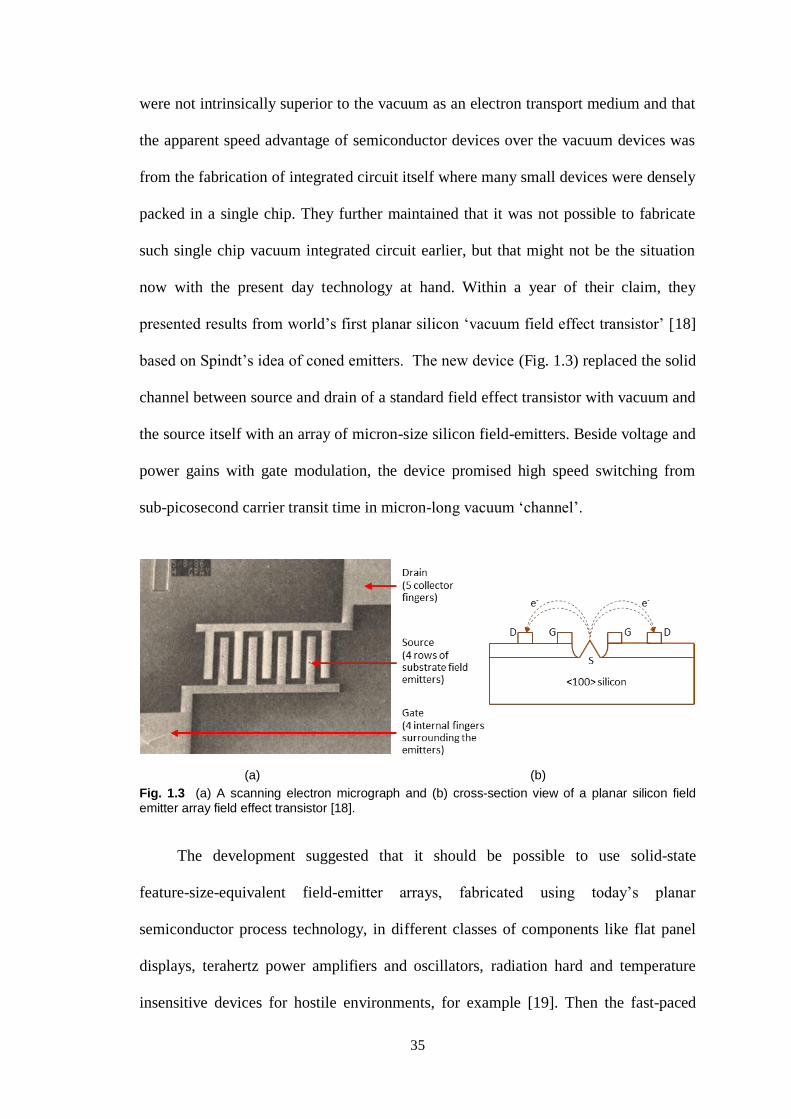
presented results from world’s first planar silicon ‘vacuum field effect transistor’ [18]
based on Spindt’s idea of coned emitters. The new device (Fig. 1.3) replaced the solid
channel between source and drain of a standard field effect transistor with vacuum and
the source itself with an array of micron-size silicon field-emitters. Beside voltage and
power gains with gate modulation, the device promised high speed switching from
sub-picosecond carrier transit time in micron-long vacuum ‘channel’.
(a) (b)
Fig. 1.3 (a) A scanning electron micrograph and (b) cross-section view of a planar silicon field emitter array field effect transistor [18].
The development suggested that it should be possible to use solid-state
feature-size-equivalent field-emitter arrays, fabricated using today’s planar
semiconductor process technology, in different classes of components like flat panel
displays, terahertz power amplifiers and oscillators, radiation hard and temperature
insensitive devices for hostile environments, for example [19]. Then the fast-paced
36
research on vacuum microelectronics began – ‘microelectronikers’ went on to produce
the miniature cold, intense electron emitters, i.e., the cathodes - the critical [20]
element required for the new revolution to become sustainable. Understanding control
of the physics, materials, and fabrication technology of the field-emitters became ever
more important and the key to the success of vacuum microelectronics [21].
Alongside, in 1986, Bennig and his group introduced ultra-sensitive Atomic
Force Microscope (AFM) capable of investigating solid surfaces, including that of
insulators, with lateral resolution of 30 Å and a vertical resolution of less than
1 Å [22]. The AFM combines the principle of STM and stylus profilometer that does
not damage the material surface. STM in AFM measures the motion of a cantilever
beam with an ultra-small mass that moves through a measurable distance (10-4
Å) even
with force as small as 10-18
N. AFM proved invaluable in the continuing research in
the nanometer domain – especially in characterization of nanomaterials.
Paradoxically, micro-fabrication technology that came as a boom for the
semiconductor solid-state devices in the past may also be a boon for the vacuum
microelectronics today. Electronics started with the ‘vacuum’ and it appears that after
a brief detour it is going to be the ‘vacuum’ again for electronics.
A brief primer on the basic phenomena related to vacuum microelectronics now
follows in order to set the scene for the work presented in the remainder of this thesis.
1.2 Work Function, Fermi Level, and Electron Emission from Metal
The behaviour of “free” electrons inside a metal can be approximately described by
the “electron gas” or Drude model. According to this model, loosely bound “free”
outer shell electrons wander freely inside the metal around immovable positive ion
cores they left behind. These “free” electrons have the maximum energy inside the
37
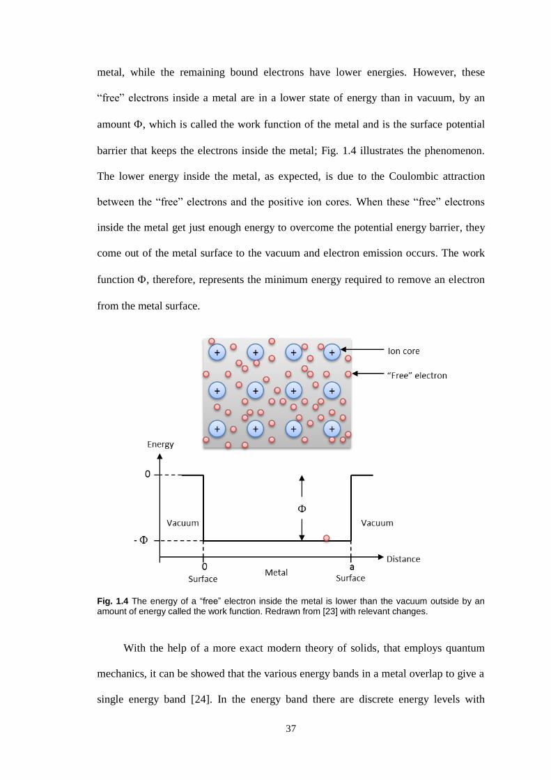
metal, while the remaining bound electrons have lower energies. However, these
“free” electrons inside a metal are in a lower state of energy than in vacuum, by an
amount , which is called the work function of the metal and is the surface potential
barrier that keeps the electrons inside the metal; Fig. 1.4 illustrates the phenomenon.
The lower energy inside the metal, as expected, is due to the Coulombic attraction
between the “free” electrons and the positive ion cores. When these “free” electrons
inside the metal get just enough energy to overcome the potential energy barrier, they
come out of the metal surface to the vacuum and electron emission occurs. The work
function , therefore, represents the minimum energy required to remove an electron
from the metal surface.
Fig. 1.4 The energy of a “free” electron inside the metal is lower than the vacuum outside by an amount of energy called the work function. Redrawn from [23] with relevant changes.
With the help of a more exact modern theory of solids, that employs quantum
mechanics, it can be showed that the various energy bands in a metal overlap to give a
single energy band [24]. In the energy band there are discrete energy levels with
38
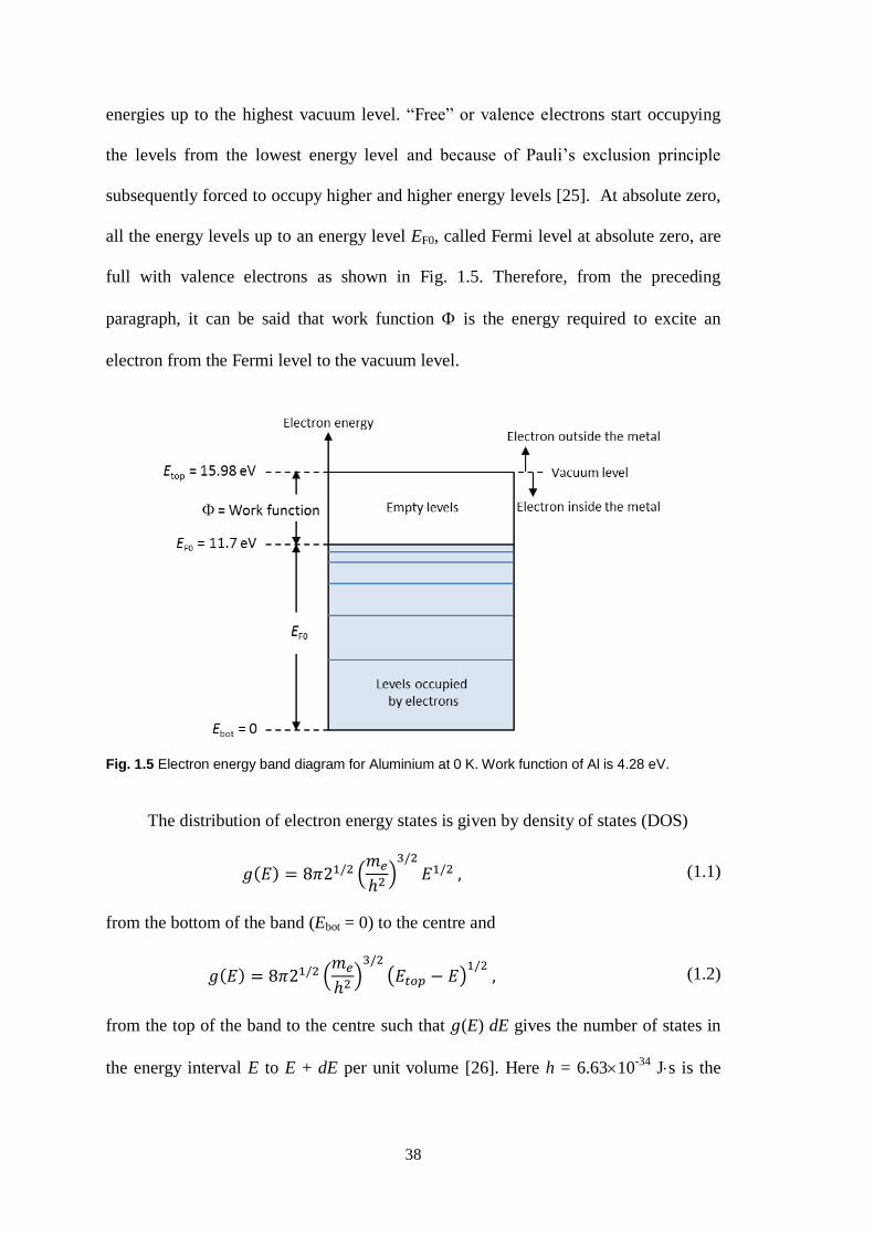
energies up to the highest vacuum level. “Free” or valence electrons start occupying
the levels from the lowest energy level and because of Pauli’s exclusion principle
subsequently forced to occupy higher and higher energy levels [25]. At absolute zero,
all the energy levels up to an energy level EF0, called Fermi level at absolute zero, are
full with valence electrons as shown in Fig. 1.5. Therefore, from the preceding
paragraph, it can be said that work function is the energy required to excite an
electron from the Fermi level to the vacuum level.
Fig. 1.5 Electron energy band diagram for Aluminium at 0 K. Work function of Al is 4.28 eV.
The distribution of electron energy states is given by density of states (DOS)
( ) ( )
(1.1)
from the bottom of the band (Ebot = 0) to the centre and
( ) ( )
( ) (1.2)
from the top of the band to the centre such that (E) dE gives the number of states in
the energy interval E to E + dE per unit volume [26]. Here h = 6.6310-34
Js is the

39
Planck’s constant, me is the electron mass. The probability of finding an electron at an
energy level E in a solid is given by the Fermi-Dirac distribution function [27]
( )
( )
(1.3)
where k = 1.3810-23 JK
-1 is the Boltzmann constant and EF is the Fermi energy, i.e.,
energy at the Fermi level. The product (E) ( ) gives the number of electrons per
unit energy per unit volume. At absolute zero, ( ) has the step form at EF; ( ) = 1
for all energy levels from Ebot up to EF and ( ) = 0 for all energy levels above EF up
to Etop. Figure 1.6, which incorporates Equations 1.1 to 1.3, shows graphically that at
absolute zero, there are no electrons available above the Fermi level.
(a) (b) (c) (d)
Fig. 1.6 (a) The density of states (E) vs. E in the energy band. (b) The Fermi-Dirac distribution at 0 K. (c) Electron concentration per unit energy nE at 0 K. (d) Electron energy band diagram at 0 K, no electrons are available above EF.
Given the background of Fermi level, work function, density of states, and
Fermi-Dirac distribution function, we look into the phenomenon of electron emission
whereby electrons are extracted from the surface of metals or semiconductors and
made available as free electrons for conduction. An energy equivalent to the work
function can be imparted to electrons in several ways so that they can escape from the

40
surface: thermionic emission, photoelectric emission, secondary emission. Besides,
electron emission is also possible if the height of the potential barrier is reduced as in
Schottky emission or the width of barrier is reduced as in field emission so that
electrons can surmount or penetrate the potential barrier even from supply of less than
the work function energy. The following sections briefly describe these electron
emission processes, while details of Schottky and field emission, the principle behind
the vacuum microelectronic devices, are discussed in more detail in Chapter 2.
1.2.1 Thermionic Emission
In thermionic emission, thermal energy in the form of heat is given to the electrons to
overcome the potential barrier. At higher temperature, the Fermi-Dirac distribution
function ( ) becomes smoother and non-zero above the Fermi level EF, and since
energy levels are available above Fermi level EF, electrons start to occupy these levels
until the electrons with enough energy, i.e., energy with work function or more,
escape the metal surface. The phenomenon is illustrated graphically in Fig. 1.7 and
represented schematically in Fig. 1.8.
(a) (b) (c) (d)
Fig. 1.7 (a) The density of states (E) vs. E in the energy band. (b) The Fermi-Dirac distribution at a high temperature, T. (c) Electron concentration per unit energy nE at T. (d) Electron energy band
diagram at T, electrons are available above EF, even up to EF + .
41
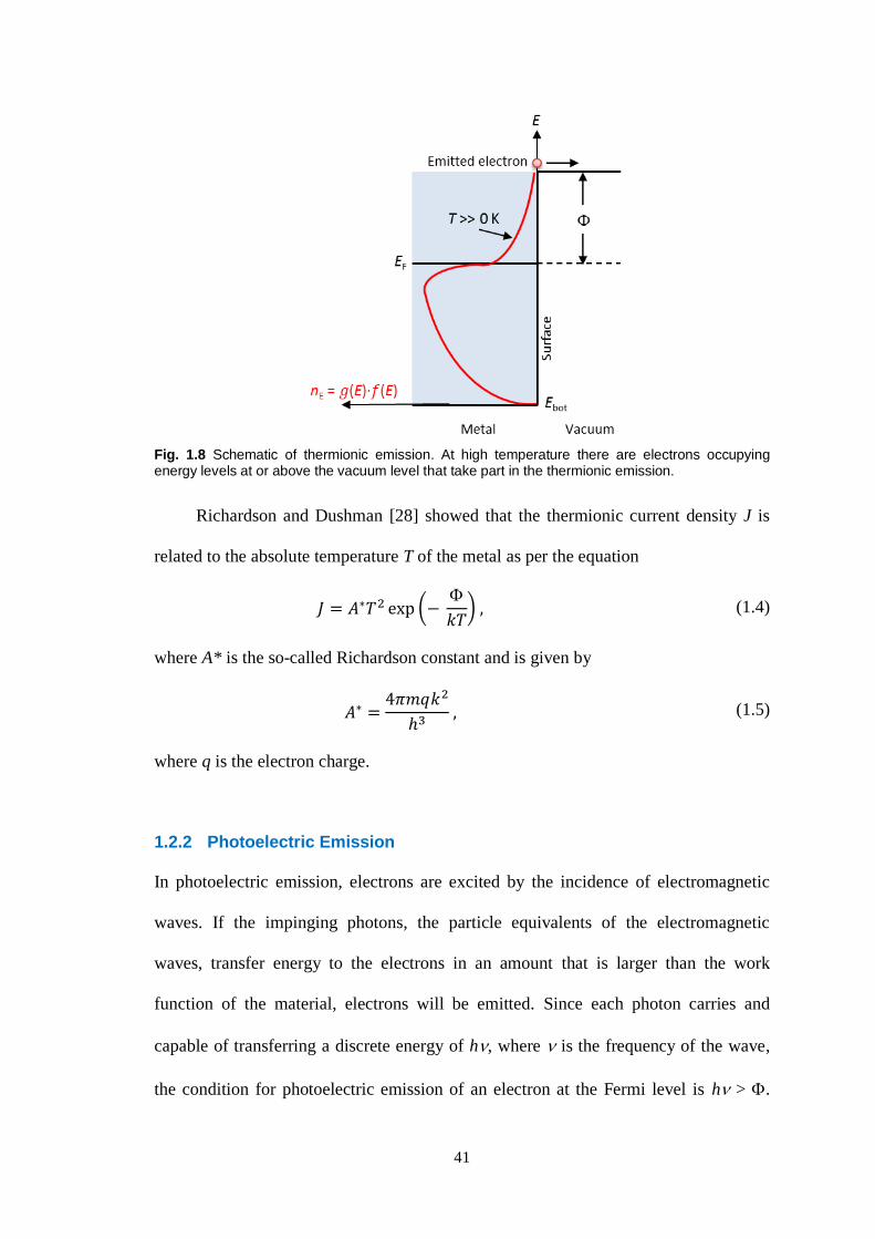
Fig. 1.8 Schematic of thermionic emission. At high temperature there are electrons occupying energy levels at or above the vacuum level that take part in the thermionic emission.
Richardson and Dushman [28] showed that the thermionic current density J is
related to the absolute temperature T of the metal as per the equation
(
) (1.4)
where A* is the so-called Richardson constant and is given by
(1.5)
where q is the electron charge.
1.2.2 Photoelectric Emission
In photoelectric emission, electrons are excited by the incidence of electromagnetic
waves. If the impinging photons, the particle equivalents of the electromagnetic
waves, transfer energy to the electrons in an amount that is larger than the work
function of the material, electrons will be emitted. Since each photon carries and
capable of transferring a discrete energy of h, where is the frequency of the wave,
the condition for photoelectric emission of an electron at the Fermi level is h > .
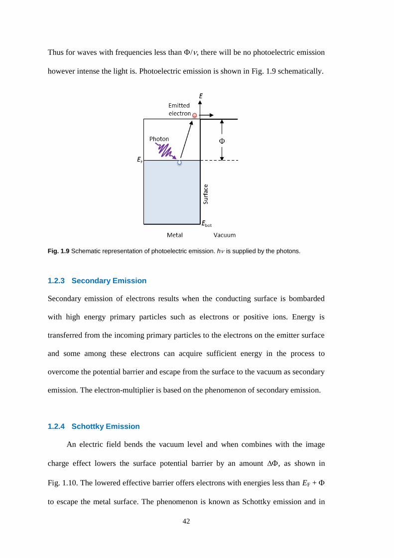
42
Thus for waves with frequencies less than /, there will be no photoelectric emission
however intense the light is. Photoelectric emission is shown in Fig. 1.9 schematically.
Fig. 1.9 Schematic representation of photoelectric emission. h is supplied by the photons.
1.2.3 Secondary Emission
Secondary emission of electrons results when the conducting surface is bombarded
with high energy primary particles such as electrons or positive ions. Energy is
transferred from the incoming primary particles to the electrons on the emitter surface
and some among these electrons can acquire sufficient energy in the process to
overcome the potential barrier and escape from the surface to the vacuum as secondary
emission. The electron-multiplier is based on the phenomenon of secondary emission.
1.2.4 Schottky Emission
An electric field bends the vacuum level and when combines with the image
charge effect lowers the surface potential barrier by an amount , as shown in
Fig. 1.10. The lowered effective barrier offers electrons with energies less than EF +
to escape the metal surface. The phenomenon is known as Schottky emission and in

43
this regime the thermionic current density equation, Eq. (1.4), when modified by the
effective barrier height, – , gives the current density for Schottky emission, JSE.
Thus,
(
( )
) (1.6)
The reduction of effective potential barrier is known as Schottky lowering effect [29].
Schottky emission will be discussed more extensively in Chapter 2.
Fig. 1.10 Schematic representation of Schottky emission. Applied field F bended the vacuum level
and lowered the original potential barrier by an amount .
1.2.5 Field Emission
As the electric field strength increases, the vacuum level bends further (refer to
Fig. 1.10) and the potential barrier becomes thinner. At intense field, the width of the
barrier becomes so small so that the electrons from inside the metal available at around
Fermi level tunnel through the barrier to vacuum resulting in electron field emission.
Fig. 1.11 is a schematic of electron field emission. Field emission can occur from
electrons at or vicinity below Fermi level at absolute zero (Fig. 1.12), and hence it is
also called “cold field electron emission.”

44
Fig. 1.11 Schematic representation of electron field emission at room temperature. Applied high electric field F bends the vacuum level so much so that electrons near Fermi level tunnel through the thin barrier.
Fig. 1.12 Schematic representation of electron field emission at absolute zero. Field emission is still possible under high electric field as electrons near Fermi level can tunnel through the thin barrier.
The field emission current density JFN under electric field F is given by the
Fowler-Nordheim equation [2]
(
) (1.7)

45
The origin of field emission from quantum-mechanical tunnelling will be discussed in
Chapter 2 where the theory of field emission is addressed in detail.
1.3 Applications of Vacuum Field Emission and Motivation
When the “come back” of vacuum tube was first reported in the New York Times in
1988, Henry Gray, one of the early leaders of the field, was quoted to say that vacuum
microelectronics (VME) “will not displace silicon technology, but will fill many
niches where it is very hard, or impossible, to use solid-state electronics” [30]. Indeed,
field emitters have potential niche applications as and in the fields of: rectifiers and
switches; displays, detectors and sensors; microwave power amplifier tubes; electron
beam lithography; ion, electron and x-ray sources. VME devices can be used in hostile
high-temperature and/or radiation environment such as in space or in where
possibilities of nuclear explosions or accidents are high.
Figure 1.13 shows schematic representations of vertical vacuum microelectronic
diodes and triodes. In these diodes, electrons are extracted from the emitter (cathode)
and collected in the collector (anode) under a strong electric field developed by
applying voltages between the collector and emitter. In the triodes, an additional
control in electron extraction is provided by gate or grid voltage. Diodes have found
applications as rectifiers and switches, and triodes as amplifiers.
Fig. 1.13 Vertical vacuum diode and triode configurations.
46
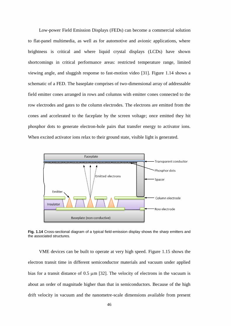
Low-power Field Emission Displays (FEDs) can become a commercial solution
to flat-panel multimedia, as well as for automotive and avionic applications, where
brightness is critical and where liquid crystal displays (LCDs) have shown
shortcomings in critical performance areas: restricted temperature range, limited
viewing angle, and sluggish response to fast-motion video [31]. Figure 1.14 shows a
schematic of a FED. The baseplate comprises of two-dimensional array of addressable
field emitter cones arranged in rows and columns with emitter cones connected to the
row electrodes and gates to the column electrodes. The electrons are emitted from the
cones and accelerated to the faceplate by the screen voltage; once emitted they hit
phosphor dots to generate electron-hole pairs that transfer energy to activator ions.
When excited activator ions relax to their ground state, visible light is generated.
Fig. 1.14 Cross-sectional diagram of a typical field-emission display shows the sharp emitters and the associated structures.
VME devices can be built to operate at very high speed. Figure 1.15 shows the
electron transit time in different semiconductor materials and vacuum under applied
bias for a transit distance of 0.5 m [32]. The velocity of electrons in the vacuum is
about an order of magnitude higher than that in semiconductors. Because of the high
drift velocity in vacuum and the nanometre-scale dimensions available from present
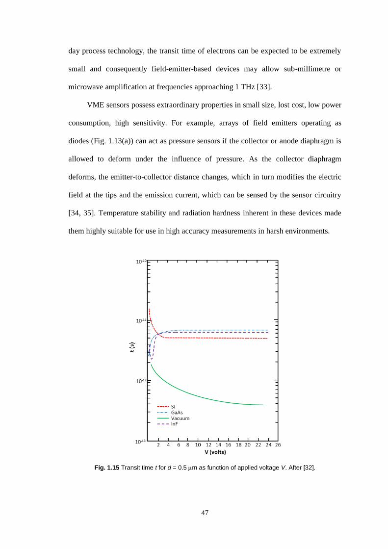
47
day process technology, the transit time of electrons can be expected to be extremely
small and consequently field-emitter-based devices may allow sub-millimetre or
microwave amplification at frequencies approaching 1 THz [33].
VME sensors possess extraordinary properties in small size, lost cost, low power
consumption, high sensitivity. For example, arrays of field emitters operating as
diodes (Fig. 1.13(a)) can act as pressure sensors if the collector or anode diaphragm is
allowed to deform under the influence of pressure. As the collector diaphragm
deforms, the emitter-to-collector distance changes, which in turn modifies the electric
field at the tips and the emission current, which can be sensed by the sensor circuitry
[34, 35]. Temperature stability and radiation hardness inherent in these devices made
them highly suitable for use in high accuracy measurements in harsh environments.
Fig. 1.15 Transit time t for d = 0.5 m as function of applied voltage V. After [32].

48
In mass spectrometry, VME allows the elimination of the hot filament as used in
thermionic emission-based devices and hence a number of common problems can be
prevented, including: thermal cracking of delicate molecules, outgassing of the
filament itself and nearby components, high power requirements for the filament, large
size, stray light, stray magnetic fields, contamination by thorium and tungsten, and
long warm-up time [36]. Recently, fabrication and operation of triode emitter as ion
source for miniature mass spectrometer has been demonstrated [37]. VME offers many
opportunities to expand on the development in the field of mass spectrometry.
Other than the Spindt-type metal field emitters, VME electron sources that are
rapidly evolving include semiconductor field emitters [38, 39, 40], carbon [41, 42],
carbon nanotubes [43, 44, 45], diamonds [46, 47], wide band gap semiconductors [48,
49, 50, 51], and negative electron affinity (NEA) materials [52, 53, 54, 55]. All seek to
minimize the barrier to electron emission into vacuum by engineering the material
properties such as the work function or the physical geometry such to change the field
enhancement factor of the cathode [56].
All these various potential applications and opportunities of vacuum
microelectronic devices led to the motivation for the present work, where fabrication
of a vacuum field emission device integrated in the CMOS-process technology was
sought. The fabrication would take advantage of using the self-assembled silicon
nanostructured emitter growth mechanism, a process developed here in New Zealand
by GNS Science [57]. It is hoped that the integration demonstrated in the work will
contribute to the advancement in the field of vacuum microelectronics.

49
1.4 Objectives of the Work
This work has four main objectives:
Study the phenomenon of electron emission from self-assembled silicon
nanostructures.
Fabrication of integrated field emission diodes using the self-assembled silicon
nanostructures as emitters.
Characterisation of the fabricated field emission diode by analysing its current-
voltage characteristics.
Develop models and carry out simulations to predict the electric field
enhancement for the self-assembled silicon nanostructures.
1.5 Dissertation Outline
Chapter 1 is a brief introduction to vacuum microelectronic devices and their
underlying principles of operation - electron emission. Early history of vacuum
microelectronics and comparative advantages of vacuum microelectronic devices over
dominant solid-state electronic devices are discussed. Potential applications of
nanostructured emitters are explored as motivation for undertaking the present work.
Objectives, motivation, and scope and outline of the present work in relation to
vacuum field emission device are also elaborated in this introductory chapter. The rest
of the dissertation is organized as follows.
Chapter 2 details the theoretical background of the physics behind the different
electron emission mechanisms in metal and its extension to semiconductor under the
influence of electric field. Fundamental theories outlined in this chapter are essential to
understand, analyse, and characterise the experimental data presented in this work. A
literature review describing different approaches and processes to construct emitters
50
and vacuum field emission devices is also presented. The GNS process to self-
assemble silicon nanostructures, which act as emitting sites for the cathode of the
planned vacuum field emission device, is introduced and the growth phenomenon of
these nanostructures is explained.
A brief review of the silicon processes and technologies and basics for atomic
force microscopy (AFM) techniques used in this work are presented in Chapter 3.
AFM principles discussed in this chapter will be useful in understanding advanced
AFM operations performed during experimentation and described in Chapter 4. The
silicon processes and technologies reviewed are ready references for Chapter 5, where
these processes and technologies were integrated to fabricate the vacuum field
emission device for this work.
Chapter 4 reports the results of the conductive AFM studies carried out on
individual self-assembled silicon nanostructures. The results were analysed for
Schottky and Fowler-Nordheim emissions. Field emission from the individual
nanostructures was also probed from a distance using interleave lift-mode AFM.
The fabrication procedure of the vacuum field-emission device incorporating the
GNS method to form self-assembled silicon nanostructures and integrated in the
CMOS process is detailed in Chapter 5. The experimental results and analysis of the
electron emission exhibited by the fabricated vacuum field emission diodes are
discussed in Chapter 6. Different electron emission regimes were identified and
explained. The techniques used to extract parameters from the current-voltage
characteristics of these devices are also explained.
Results of modelling of field enhancements in the cases of both the individual
nanostructure-AFM tip contact and device electrodes are made and results are reported
in Chapter 7. Finally, Chapter 8 presents the overall summary and conclusions of the

51
present work. Limitations of the present work are discussed and future directions for
work needed to advance the research in order to optimise the device fabrication
process and to extend the study to include integrated vacuum triode are suggested.

52

53
Chapter 2
BACKGROUND – FIELD EMISSION, FIELD EMITTERS,
AND FIELD-EMISSION DEVICES
The background material covered in this chapter is divided into two major parts: the
theoretical part draws on field emission from solids along with field-enhanced
thermionic and thermo-field emission, and the experimental part addresses fabrication
of field emitters and field-emission devices. The theory of field emission includes the
origins of Schottky barrier lowering and Fowler-Nordheim tunnelling under applied
field, and of relevant current equations in metals. The result is extended to emission
from semiconductors. In addition, the phenomenon of local field enhancement at
emitter tips is discussed and modelled in a separate section.
The various methods to fabricate field emitters and field-emission devices are
recorded through literature review while the GNS process to grow self-assembled
silicon nanostructured emitters is detailed in an independent section. These
nanostructured emitters are the building blocks that constitute the cathode of the
fabricated integrated field emission device, fabrication of which is the major objective
of the present work and which is the topic of Chapter 5.
54
2.1 Electron Emission from Metals under the Influence of Electric Fields
Although the present work deals with electron emission from a semiconductor surface,
an account of the same from a metal surface is first discussed in this section, which is
necessary to build the theoretical foundation on the subject. The more complex theory
of electron emission from semiconductors will be addressed in Section 2.2.
2.1.1 Tunnelling of Electrons through Narrow Potential Barrier
The phenomenon of emission of electrons from the surface of a condensed phase
(usually a metal or a semiconductor) into another phase (classically a vacuum) under
the influence of high applied field (typically 3 - 6 107
V/cm) is defined as field
emission [58]. Electron field emission is essentially a quantum-mechanical
phenomenon – the tunnelling or leaking of electrons near the Fermi level through a
low but more importantly narrow potential barrier. The narrowness of the barrier is a
consequence of high applied field.
We can find the minimum barrier width a and the condition for tunnelling in the
case of a metal with work function and applied field F using a simple model, shown
schematically in Fig. 2.1. In this model, the contribution from the surface image
potential, which is described in Section 2.1.2, is neglected. An electron near the Fermi
level requires kinetic energy equal to barrier height from Fermi level, i.e., work
function (Fig. 2.1) to escape the metal surface. Now, for the electron having such
energy with mass m and momentum 2
1
2 mp (from m
pmv
22
1 2
2 , where
mvp ), the related uncertainty of momentum is given by 2
1
22 mp for the
momentum is uncertain in + p to - p.
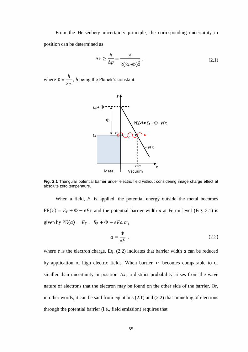
55
From the Heisenberg uncertainty principle, the corresponding uncertainty in
position can be determined as
( )
(2.1)
where 2
h , h being the Planck’s constant.
Fig. 2.1 Triangular potential barrier under electric field without considering image charge effect at absolute zero temperature.
When a field, F, is applied, the potential energy outside the metal becomes
( ) and the potential barrier width a at Fermi level (Fig. 2.1) is
given by ( ) or,
(2.2)
where e is the electron charge. Eq. (2.2) indicates that barrier width a can be reduced
by application of high electric fields. When barrier a becomes comparable to or
smaller than uncertainty in position x , a distinct probability arises from the wave
nature of electrons that the electron may be found on the other side of the barrier. Or,
in other words, it can be said from equations (2.1) and (2.2) that tunneling of electrons
through the potential barrier (i.e., field emission) requires that

56
( )
(2.3)
or, that
( )
(2.4)
The simple relation of Eq. (2.4) specifies that metals with higher work functions
will require higher electric fields for field emission. Calculated minimum field
requirements for tunnelling from various metals with their work functions are plotted
in Fig. 2.2.
Fig. 2.2 Minimum field requirements (theoretical) for field emissions from common metals are plotted with respect to their work functions. Values for work function considered are the minimum values taken from ref. [59] from among values of different planes for a given metal.
Figure 2.2 shows that fields in the range of 108 V/cm are required for most
metals for field emission to occur. However, it has been found experimentally that
fields capable of initiating electron emission are in fact 10-50 times lower than these
theoretical values, i.e., are in the 107 V/cm range [60].

57
2.1.2 Image Effect and Schottky Barrier Lowering
In electrostatics, the theorem of image charges stipulates that an electron with charge
at a distance x in front of an infinitely conducting sheet experiences a force as if
there were a ‘mirror’ positive charge of at a distance x behind the sheet and is
illustrated in Fig. 2.3 [61]. The relevant image force between the two charges,
therefore, is
( )
(2.5)
And its integration from point x to infinity, which gives the potential energy from the
image charge effect is
( ) ∫ ( )
(2.6)
Fig. 2.3 The ‘image charge’ theorem. The effect of a plane conductor on the static field due to a charged particle is equivalent to a second, oppositely charged, particle in the mirror image position. After reference [61].
A more accurate relation for the tunnelling condition found in Eq. (2.4) requires
incorporation of contributions from the surface image potential that lowers the
potential barrier height by an amount . The lowering of the potential barrier height
from image charge effects under applied electric field is termed as Schottky lowering
effect [29]. The reduced work function, eff, (Fig. 2.4) can be calculated by finding the

58
maximum of the net potential energy outside the metal surface under applied field F,
which now is given by
( ) ( )
(2.7)
Fig. 2.4 Schottky “barrier lowering” from the image charge effect. The applied field is 6x10⁷ V/cm.
After reference [62].
The location of the maximum of PE(x) can be found by differentiating Eq. (2.7)
and setting it to zero. Thus, 01
16 2
0
2
eFx
e
, which gives PE(x)max at
(
)
(2.8)
Noting the PE(x)max equals , we get an effective work function from Eq. (2.7)
(
)
(2.9)
The Schottky barrier lowering amount becomes
(
)
(2.10)

59
2.1.3 Quantum Mechanical Tunnelling through Single Rectangular Potential Barrier
The effective barrier width can be found from Eq. (2.6), noting the PE(x) at x1 and x2
to be EF:
( ) [(
)
]
(2.11)
For high fields, from Eq. (2.11) together with Eq. (2.2), we have
(2.12)
Since the field emission is normal to the metal surface, the tunnelling event, in
its simplest approximate form, then reduces to a one-dimensional (1-D) quantum
mechanical potential barrier problem of an electron with EF kinetic energy
encountering a rectangular barrier of height EF + and width a. The approximation is
illustrated in Fig. 2.5.
Fig. 2.5 Electron emission from metal surface can at the simplest form be modelled approximately as a quantum mechanical problem of an electron with EF kinetic energy encountering a rectangular
barrier of height EF + and width a.
Solving Schrödinger equations for this simplified potential energy environment
subject to conditions that wave functions and their first derivatives are continuous at
0x and at ax , we obtain the transmission coefficient T(E) [63]:

60
( ) [ ( )
{(
)
}]
(2.13)
For the values of and a with which we are concerned, 12 2
1
2
a
m
, and
therefore,
a
ma
m 2
1
2
2
1
2
2exp
2
12sinh
. Thus Eq. (2.13) can be rewritten as,
( )
( ) [ (
)
] (2.14)
Eq. (2.14) indicates that the tunnelling probability, which is represented by the
transmission coefficient T(E), decreases exponentially with the width of the barrier a
and the square root of the barrier height .
2.1.4 Tunnelling through Triangular Potential Barrier
For the case of a triangular energy barrier (Fig. 2.1) or barrier with image
potential (Fig. 2.4), the determination of transmission coefficient becomes non-trivial.
Using the Wentzel, Kramers, and Brilluoin or WKB approximation [64], where the
complex tunneling barrier is treated in a piecewise manner, an equivalent for
Eq. (2.14) can be worked out analytically for the reduced energy barrier with image
charge effect giving the Fowler-Nordheim tunneling transmission co-efficient [65]
( ) (
√
( )) (2.15)
and the field emission current density
( ) (
( )) (2.16)

61
where ( ) and ( ) are the Nordheim functions that incorporate the image charge
effects. The values for ( ) and ( ) had been tabulated and can be found in reference
[66].
When the image charge effects are ignored, the Fowler-Nordheim transmission
coefficient and equation with the triangular energy barrier reduce respectively to
[67,68]
( ) (
√
) (2.17)
and
(
) (2.18)
The approach discussed here is extended with appropriate changes to determine
current from a semiconductor emitter in Section 2.2.
2.1.5 Schottky Emission
In Schottky emission, electrons having thermal energy which is less than the energy
required to overcome the potential barrier take advantage of a lower effective potential
barrier to escape the metal surface. The lowering of effective potential barrier is
known as Schottky lowering and results from the image charge effect and the applied
field as described in Section 2.1.2. The lowered amount is given by Eq. (2.10). We
recall the Schottky emission Eq. (1.6) and rewrite the same substituting for the
effective work function as
(
( )
) (2.19)
Eq. (2.19) reduces to the thermionic case (Eq. (1.4)) at very low electric fields.
As the field increases, Eq. (2.19) describes the effect of lowering of the potential
62
barrier. However, it has been shown that the Schottky equation holds good for fields
up to 106 V/cm [69]. At higher fields, considerable tunneling current contributes to the
overall current density. A dimensionless parameter given by
( )
(2.20)
measures satisfactorily the tunneling current contribution [70, 71]; q = 0 indicates no
tunneling, whereas for q = 1, there is only tunneling. When q is small, i.e. when a
small fraction of the current is due to tunneling, typically < 0.3, the Schottky equation
adequately describes the emission characteristics.
2.1.6 Extended Schottky Emission and the Transition Region
Between electric fields of 106 V/cm and 10
7 V/cm, neither the Schottky emission, nor
the Fowler-Nordheim emission alone adequately describes the emission current. This
is the transition region where electrons from both above and below the top of the
potential barrier, usually well above the Fermi level, contribute significantly to the
total emitted current. The emission mechanism for the situation is shown in Fig. 2.6.
The total current density from such emission can be approximated by the following
extended Schottky emission equation [72]
( ) (2.21)
The region has been shown to be bounded by the q values [Eq. 2.20] from 0.3 to
0.7 [71]. At q = 0.5, which lies in the middle of this transition region, exactly one-half
of the total emission current is due to electrons surmounting the potential barrier and
one-half due to electrons tunnelling through the potential barrier.
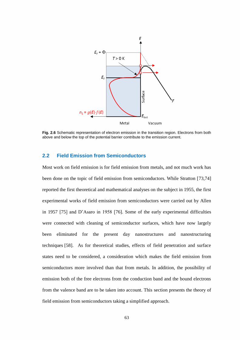
63
Fig. 2.6 Schematic representation of electron emission in the transition region. Electrons from both above and below the top of the potential barrier contribute to the emission current.
2.2 Field Emission from Semiconductors
Most work on field emission is for field emission from metals, and not much work has
been done on the topic of field emission from semiconductors. While Stratton [73,74]
reported the first theoretical and mathematical analyses on the subject in 1955, the first
experimental works of field emission from semiconductors were carried out by Allen
in 1957 [75] and D’Asaro in 1958 [76]. Some of the early experimental difficulties
were connected with cleaning of semiconductor surfaces, which have now largely
been eliminated for the present day nanostructures and nanostructuring
techniques [58]. As for theoretical studies, effects of field penetration and surface
states need to be considered, a consideration which makes the field emission from
semiconductors more involved than that from metals. In addition, the possibility of
emission both of the free electrons from the conduction band and the bound electrons
from the valence band are to be taken into account. This section presents the theory of
field emission from semiconductors taking a simplified approach.
64
2.2.1 Supply of Electrons and the Simplest Model of Electron Emission from Semiconductors
The carrier concentrations of an intrinsic, an n-type, and a p-type semiconductor along
with the simplified band diagram, density of state, and Fermi-Dirac distribution
function are shown in Fig. 2.7. The figure shows that, unlike in a metal, the Fermi
level is observed to shift in a semiconductor from its intrinsic position of the middle of
the bandgap to adjust itself to preserve charge neutrality when donor (of concentration
ND) or acceptor (of concentration NA) are introduced into the semiconductor. For an n-
type semiconductor, the Fermi level shifts towards the conduction band shifting the
Fermi-Dirac distribution function with it resulting in a higher electron concentration in
the conduction band than that from the intrinsic case at thermal equilibrium at a
temperature higher than 0 K. Whereas, for the analogous situation in a p-type
semiconductor, the Fermi level shifts towards the valence band and results lower, but
not zero, electron concentration in the conduction band. Free electrons for tunneling
under high electric fields are, therefore, available in the conduction band in all three
types of semiconductors at non-absolute-zero temperature.
The Fermi level, though shifting its position, remains inside the bandgap during
these adjustments. However, the shifting of Fermi level with no electrons inside the
bandgap has no other consequences with respect to electron tunneling from the
bandgap energy locations. As for the valence band, which is a full band where no
empty states are available for electron conduction, the tunneling of bound electrons
may theoretically occur from the top of the valence band into the vacuum, if the
applied external field presents a barrier width just narrow enough for such emission.
Since each emitted electron leaves a positive hole in the valence band, which is to be

65
balanced by another electron from the bulk, there will be enough conduction to sustain
the emission current [58].
(a)
(b)
(c)
Fig. 2.7 (From left) Schematic band diagram, density of states, Fermi-Dirac distribution function, and the carrier concentrations for (a) intrinsic, (b) n-type, and (c) p-type semiconductors at thermal
equilibrium at T, where T 0 K. ND, NA are the donor and acceptor impurities concentrations. After Sze [77].
In its simplest form, therefore, a parallel can be drawn between field emission
from metals and semiconductors noting that the surface potential barrier height from
the bottom of the conduction band is the electron affinity for emission from

66
conduction band, and from the top of the valence band it is + Eg for emission from
valence band. Eg is the bandgap that separates the conduction band from the valence
band. This simple model of electron emission from a semiconductor is illustrated
in Fig. 2.8. The corresponding Fowler-Nordheim current from semiconductor
conduction and valence band will be given by Eq. (2.18) with and + Eg
respectively replacing .
Fig. 2.8 Schematic of the simplest model of field emission from an n-type semiconductor. The model is same for p-type semiconductor too. Electrons at the bottom of the conduction band
encounter a potential barrier of height and width a at field F1, while for electrons at the top of the
valence band the barrier height is + Eg. For the tunneling from top of the valence band to be significant at the same barrier width a, a higher field F2 is required.
2.2.2 Field Penetration Effect
The simple model of field emission is not critically realistic as the external electric
field penetrates into the semiconductor and both the conduction and valence bands
bend at the surface, as shown in Fig. 2.9. Two cases can arise at the conduction band:
1) If the conduction band is bent by an energy V0 not sufficient to bring it below
the Fermi level as presented in Fig. 2.9(a), the electrons at the bottom of the
conduction band encounters a barrier of height as before the field penetration being

67
considered. However, the Fowler-Nordheim current density would require to be
multiplied by a factor representing the increased electron concentration at the
bottom of the bent conduction band [58]. This situation can arise in an intrinsic
semiconductor where Fermi level is in the middle of the bandgap or in a lightly doped
n-type semiconductor where it is a considerable distance away from the conduction
band edge.
(a) (b)
Fig. 2.9 Field emission from the conduction band of an n-type semiconductor with field penetration. The conduction band has bent but (a) has not dipped below the Fermi level, and (b) has dipped below the Fermi level near the semiconductor surface.
2) If at high field, V0 is sufficient to bring the bottom of the conduction band
below the Fermi level, as in a moderately to highly doped n-type semiconductor where
Fermi level lies close to the conduction band, electrons collect in the dip as depicted in
Fig. 2.9(b). It is evident that the highest filled level of the collection coincides with the
Fermi level, which remains constant throughout the semiconductor. In this case, the
barrier height is reduced by an amount and the effective barrier height for the
Fowler-Nordheim equation is given by
( ) (2.22)

68
Gomer [58] evaluated as
(2.23)
where,
(2.24)
for F in V/cm, energies in eV. s is the dielectric constant of the semiconductor.
The field penetration has no effect in emission from semiconductor valence band
as barrier height + Eg remains unchanged at the semiconductor surface even with the
bent valence band. The situation is apparent in Fig. 2.9.
2.2.2 Image Charge Effect
The image force correction for a semiconductor with dielectric constant s is the factor
[73] that goes into the barrier height adjustment in square root form as in
Eq. (2.6). For our semiconductor of interest, silicon, s = 11.9 and, therefore,
= 0.85 and √
= 0.92 1. The image charge effect, therefore, for all the
practical purposes, needs no significant correction for emission from silicon.
2.3 Field Enhancement and Emitter Shape
A large external electric field, typically in the 107 V/cm range, is required to realize
field emission from most metals. The same requirement is true for emission from a
semiconductor, for example, from silicon, as the electron affinity for silicon is
4.05 eV, which is the effective work function for emission from the bottom of its
conduction band. For flat and parallel electrodes, the field 0F is related to the applied
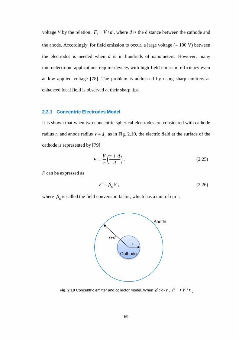
69
voltage V by the relation: dVF /0 , where d is the distance between the cathode and
the anode. Accordingly, for field emission to occur, a large voltage ( 100 V) between
the electrodes is needed when d is in hundreds of nanometers. However, many
microelectronic applications require devices with high field emission efficiency even
at low applied voltage [78]. The problem is addressed by using sharp emitters as
enhanced local field is observed at their sharp tips.
2.3.1 Concentric Electrodes Model
It is shown that when two concentric spherical electrodes are considered with cathode
radius r, and anode radius dr , as in Fig. 2.10, the electric field at the surface of the
cathode is represented by [79]
(
) (2.25)
F can be expressed as
(2.26)
where is called the field conversion factor, which has a unit of cm-1
.
Fig. 2.10 Concentric emitter and collector model. When rd , rVF / .

70
Here, when dr , dVF / and the arrangement becomes that of flat
parallel electrodes. But, when rd , rVF / . In the latter case, the field
conversion factor approaches 1/r and the required large field for emission results if
r is in the order of nanometers, even at low applied voltages. The result calls for sharp
pointed, i.e., with nanometer r, emitters for low voltage field emission.
2.3.2 Rounded Whisker Model
Many different geometrical shapes of sharp field emitters have been suggested
over time and typical ones being shown in Fig. 2.11. When the figure of merit f, which
measures maximum current with minimum voltage and linear dimension capability is
compared for emitters with different shapes, the rounded whisker provided the highest
value [21].
(a) (b) (c) (d)
Fig. 2.11 Various shapes of sharp field emitters: (a) rounded whisker, (b) sharpened pyramid, (c)
hemi-spheroidal, and (d) pyramidal. is the half-angle at the tip. After Utsumi [21].
The local field at the apex of a rounded whisker protruding out of an infinite
plane is calculated to be
(
) (2.27)
where h is the height, r the radius of the whisker, and F0 the flat parallel-plane electric
field [80].
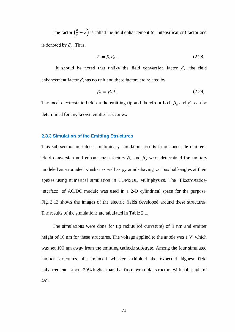
71
The factor (
) is called the field enhancement (or intensification) factor and
is denoted by . Thus,
(2.28)
It should be noted that unlike the field conversion factor , the field
enhancement factor has no unit and these factors are related by
(2.29)
The local electrostatic field on the emitting tip and therefrom both and can be
determined for any known emitter structures.
2.3.3 Simulation of the Emitting Structures
This sub-section introduces preliminary simulation results from nanoscale emitters.
Field conversion and enhancement factors and were determined for emitters
modeled as a rounded whisker as well as pyramids having various half-angles at their
apexes using numerical simulation in COMSOL Multiphysics. The ‘Electrostatics-
interface’ of AC/DC module was used in a 2-D cylindrical space for the purpose.
Fig. 2.12 shows the images of the electric fields developed around these structures.
The results of the simulations are tabulated in Table 2.1.
The simulations were done for tip radius (of curvature) of 1 nm and emitter
height of 10 nm for these structures. The voltage applied to the anode was 1 V, which
was set 100 nm away from the emitting cathode substrate. Among the four simulated
emitter structures, the rounded whisker exhibited the expected highest field
enhancement – about 20% higher than that from pyramidal structure with half-angle of
45°.
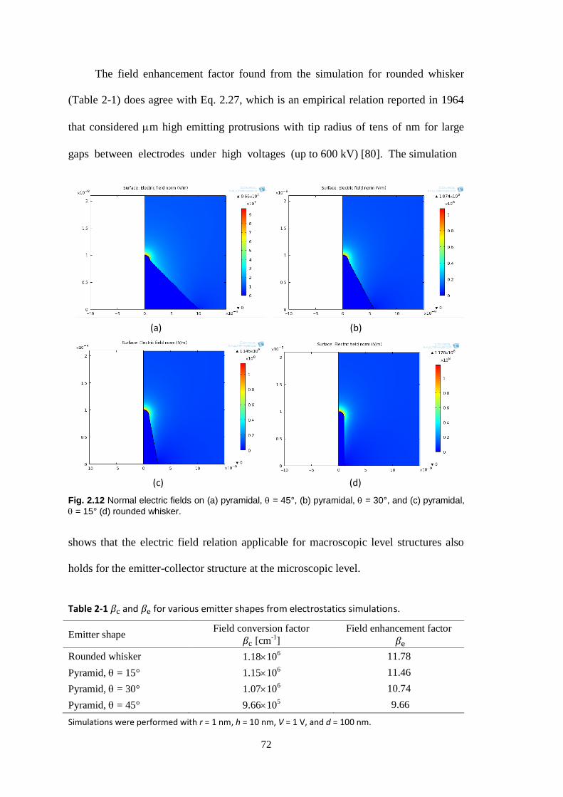
72
The field enhancement factor found from the simulation for rounded whisker
(Table 2-1) does agree with Eq. 2.27, which is an empirical relation reported in 1964
that considered m high emitting protrusions with tip radius of tens of nm for large
gaps between electrodes under high voltages (up to 600 kV) [80]. The simulation
(a) (b)
(c) (d)
Fig. 2.12 Normal electric fields on (a) pyramidal, = 45°, (b) pyramidal, = 30°, and (c) pyramidal,
= 15° (d) rounded whisker.
shows that the electric field relation applicable for macroscopic level structures also
holds for the emitter-collector structure at the microscopic level.
Table 2-1 and for various emitter shapes from electrostatics simulations.
Emitter shape Field conversion factor
[cm-1
]
Field enhancement factor
Rounded whisker 1.18106 11.78
Pyramid, = 15° 1.15106 11.46
Pyramid, = 30° 1.07106 10.74
Pyramid, = 45° 9.66105 9.66
Simulations were performed with r = 1 nm, h = 10 nm, V = 1 V, and d = 100 nm.

73
The details of the simulation including the problem space, its boundary
conditions, and the finite element meshing scheme are discussed in Chapter 7, where
results from the modelling and simulation of the GNS nanostructures are also reported.
2.3.4 General Comments on Emitter Shapes
Since a very thin defect-free SiO2 film, which is the common insulator used in silicon
technology, exhibits an intrinsic breakdown limit of 107 V/cm, we can realize a sharp
emitter with enough leverage in oxide breakdown by exploiting the field enhancement
factor. For example, if a design oxide breakdown limit of 5106 V/cm is set as the
maximum allowed F0 for the device structure, a > 6 would suffice for field emission
at 3107 V/cm from emitter tip without exposing the structure to oxide breakdown. A
rounded whisker with a radius of 1 nm requires a height of 6 nm or more to meet the
requirement for this example.
Thermal stability of the rounded whisker is poor for the high temperature
gradient that develops at its root and Utsumi [21] suggested smaller dimension emitter
with an Eiffel Tower shape as both high figure of merit and thermally stable ideal
emitter. The smaller dimension of the emitters reduces the possibility of their thermal
‘blow-ups’ from heat generation at high current densities. The self-assembled
nanostructured emitters as grown by GNS method [57] provide a close match to the
ideal Eiffel Tower shape.
2.4 Fabrication of Field Emitters
Fabrication of nanometer scale, thermally stable and high f (figure of merit) field
emission emitters presents the greatest challenge in the development of vacuum
microelectronic devices. Several techniques with various materials are demonstrated to
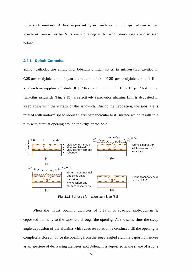
74
form such emitters. A few important types, such as Spindt tips, silicon etched
structures, nanowires by VLS method along with carbon nanotubes are discussed
below.
2.4.1 Spindt Cathodes
Spindt cathodes are single molybdenum emitter cones in micron-size cavities in
0.25 m molybdenum - 1 m aluminum oxide - 0.25 m molybdenum thin-film
sandwich on sapphire substrate [81]. After the formation of a 1.5 1.5 m2 hole in the
thin-film sandwich (Fig. 2.13), a selectively removable alumina film is deposited in
steep angle with the surface of the sandwich. During the deposition, the substrate is
rotated with uniform speed about an axis perpendicular to its surface which results in a
film with circular opening around the edge of the hole.
Fig. 2.13 Spindt tip formation technique [81].
When the target opening diameter of 0.5 m is reached molybdenum is
deposited normally to the substrate through the opening. At the same time the steep
angle deposition of the alumina with substrate rotation is continued till the opening is
completely closed. Since the opening from the steep angled alumina deposition serves
as an aperture of decreasing diameter, molybdenum is deposited in the shape of a cone

75
on the base of the hole. The closure film is then removed through selective etching to
obtain the molybdenum emitter.
2.4.2 Silicon Etched Structures
Sub-50 nm diameter silicon pillars (Fig. 2.14) have been fabricated using high
resolution electron lithography and anisotropic reactive ion etching followed by
thermal oxidation of the as-etched structures [82]. Here a 40 keV, 10 pA electron
beam of diameter 5 nm is used to pattern array of dots on a 50 nm poly-methyl-
methacrylate (PMMA) film on top of a 100 nm thermally grown SiO2. After the
development of the resist, a 10 nm thick Cr film is deposited via e-beam evaporation
and then a lift-off defines the Cr dot pattern, which acts as the mask for the RIE of
oxide layer. Etching of the oxide layer is performed with CHF3 and O2 gases and then
the etching of the silicon layer with Cl2 and SiCl4 with etched and patterned oxide
layer as mask. With this sub-50 nm silicon columns with an aspect ratio of more than 7
to 1 are obtained. To reduce the diameter of the silicon pillars further, dry oxidation is
carried out at 700 to 850˚C.
(a) (b) (c)
Fig, 2.14 SEM micrographs of (a) sub-50 nm Cr dot patterns defined by electron beam lithography and liftoff process, and (b) sub-50 nm wide Si columnar structures defined by RIE using SiO2 as a mask. (c) A series of TEM micrographs showing an identical Si column going through (i) 3 h, (ii) 4 h, and (iii) 5 h of dry oxidation at 850 °C. After 5 h, the entire Si core was consumed in the neck region. From ref [82].
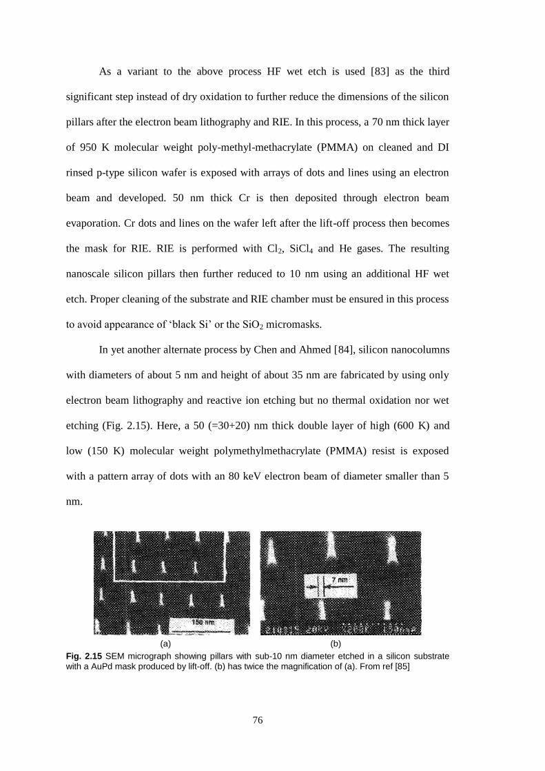
76
As a variant to the above process HF wet etch is used [83] as the third
significant step instead of dry oxidation to further reduce the dimensions of the silicon
pillars after the electron beam lithography and RIE. In this process, a 70 nm thick layer
of 950 K molecular weight poly-methyl-methacrylate (PMMA) on cleaned and DI
rinsed p-type silicon wafer is exposed with arrays of dots and lines using an electron
beam and developed. 50 nm thick Cr is then deposited through electron beam
evaporation. Cr dots and lines on the wafer left after the lift-off process then becomes
the mask for RIE. RIE is performed with Cl2, SiCl4 and He gases. The resulting
nanoscale silicon pillars then further reduced to 10 nm using an additional HF wet
etch. Proper cleaning of the substrate and RIE chamber must be ensured in this process
to avoid appearance of ‘black Si’ or the SiO2 micromasks.
In yet another alternate process by Chen and Ahmed [84], silicon nanocolumns
with diameters of about 5 nm and height of about 35 nm are fabricated by using only
electron beam lithography and reactive ion etching but no thermal oxidation nor wet
etching (Fig. 2.15). Here, a 50 (=30+20) nm thick double layer of high (600 K) and
low (150 K) molecular weight polymethylmethacrylate (PMMA) resist is exposed
with a pattern array of dots with an 80 keV electron beam of diameter smaller than 5
nm.
(a) (b)
Fig. 2.15 SEM micrograph showing pillars with sub-10 nm diameter etched in a silicon substrate with a AuPd mask produced by lift-off. (b) has twice the magnification of (a). From ref [85]
77
After exposure the resist is rapidly developed in 3:7 cellusolve:methanol with
ultrasonic agitation during the development. A 5 nm thick AuPd film is deposited by
ionized beam evaporation and a metal pattern of sub-10 nm dots is obtained by liftoff.
The AuPd pattern is then used as a mask on the Si substrate which is etched with
reactive ion etching in a gas flow of 10 sccm SiC14 and 20 sccm CF4, with 20 mTorr
chamber pressure and 200 W etching power for an etching time of 25 s. Resulting
nanocolumns exhibit necks between the tips and the bases and the electron-beam
lithography limits throughput in this technique.
2.4.3 VLS Method
Vapour-liquid-solid (VLS) growth has been the most extensively used method to grow
group IV, III–V, and II–VI semiconductor nanowires [86]. Wagner and Ellis proposed
the VLS mechanism to grow silicon whiskers of 100 nm in diameter in 1964 [87]. In
this mechanism, an impurity is introduced on the substrate to form a liquid alloy
droplet of comparatively lower freezing temperature than that of silicon. The liquid
alloy droplet then becomes the preferred sink for the arriving Si atoms of the vapor
source, a mixture of hydrogen and SiCl4. The Si enters the liquid alloy droplet and
freezes out with a very small concentration of impurity in solid solution at the
interface between solid Si and the liquid alloy. With continuation of the process, the
alloy droplet becomes displaced from the substrate and ‘rides’ on top of the whisker as
the whisker grows in length (Fig. 2.16). The growth continues till the impurity is
consumed or the growth conditions are changed. Any of Au, Pt, Ag, Pd, Cu or Ni can
be used as the impurity for the VLS growth of silicon. Growth of silicon
nanostructures is controlled through appropriate use of impurities in patterns or films
on substrate surfaces.
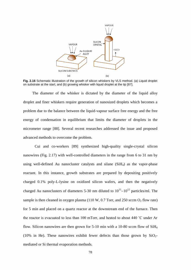
78
Fig. 2.16 Schematic illustration of the growth of silicon whiskers by VLS method. (a) Liquid droplet on substrate at the start, and (b) growing whisker with liquid droplet at the tip [87].
The diameter of the whisker is dictated by the diameter of the liquid alloy
droplet and finer whiskers require generation of nanosized droplets which becomes a
problem due to the balance between the liquid-vapour surface free energy and the free
energy of condensation in equilibrium that limits the diameter of droplets in the
micrometer range [88]. Several recent researches addressed the issue and proposed
advanced methods to overcome the problem.
Cui and co-workers [89] synthesized high-quality single-crystal silicon
nanowires (Fig. 2.17) with well-controlled diameters in the range from 6 to 31 nm by
using well-defined Au nanocluster catalysts and silane (SiH4) as the vapor-phase
reactant. In this instance, growth substrates are prepared by depositing positively
charged 0.1% poly-L-lysine on oxidized silicon wafers, and then the negatively
charged Au nanoclusters of diameters 5-30 nm diluted to 101110
12 particles/ml. The
sample is then cleaned in oxygen plasma (110 W, 0.7 Torr, and 250 sccm O2 flow rate)
for 5 min and placed on a quartz reactor at the downstream end of the furnace. Then
the reactor is evacuated to less than 100 mTorr, and heated to about 440 ˚C under Ar
flow. Silicon nanowires are then grown for 5-10 min with a 10-80 sccm flow of SiH4
(10% in He). These nanowires exhibit fewer defects than those grown by SiO2-
mediated or Si thermal evaporation methods.

79
Fig. 2.17 (a) Schematic illustrating size-controlled synthesis of SiNWs from Au nanoclusters. (b) AFM image of 10 nm Au nanoclusters dispersed on the substrate (left). FESEM image of SiNWs
grown from the 10 nm nanoclusters (right). The sides of both images are 4m. The inset in the right image is a TEM micrograph of a 20.6-nm-diam SiNW with a Au catalyst at the end. The scale bar is 20 nm. From ref. [89].
2.4.4 Laser Ablation VLS Method
The laser ablation method for synthesis of silicon nanowire is due to Alfredo Morales
and Charles Lieber [90]. Here (Fig. 2.18) the output of a pulsed Nd-yttrium-aluminum-
garnet laser (wavelength 532 nm, energy h ) is focused onto a Si0.9Fe0.1 source-
catalyst target at 1200˚C located in a quartz tube. The ablation results in dense hot
vapour plasma of Si and Fe species which upon collision with a flowing buffer gas
quickly condenses into liquid Si-rich Si-Fe nanoclusters. When the liquid
supersaturates, the co-existing Si phase precipitates and crystallizes as nanowires
completing the VLS growth process. The growth of the nanowires continues as long as
the Si-Fe nanoclusters remain in liquid state and the Si species are available and
terminates when the nanowires pass out of the hot reaction zone and are collected by
the cold finger and as the Si-Fe nanoclusters solidify.

80
Fig. 2.18. Schematic of laser ablation VLS method to grow silicon nanowire [90].
Although the laser ablation method has been successfully applied to grow
nanowires of various semiconductor materials, the wire diameters have exhibited large
size distributions [91].
2.4.5 SLS Synthesis
Korgel and co-workers reported growth of Si [92] and Ge [91] nanowires with
diameters of 5 and 10 nm respectively and with lengths of several micrometers using
2.5 nm diameter seed alkanethiol-protected gold nanocrystals dispersed in supercritical
hexane fluid heated and pressurized above its critical point. Diphenylsilane was used
as precursor for silicon and traethylgermane and diphenylgermane were used
independently as germanium precursors in the fluid. Growth proceeded (Fig. 2.19)
through a solution-liquid-solid (SLS) mechanism at growth temperatures below 500
˚C. The silicon and germanium nanowires grown have shown nearly uniform diameter.
Fig. 2.19 Schematic of nanowire growth process: thermal degradation of diphenylsilane results in free Si atoms that dissolve in the Au nanocrystal until reaching a Si:Au alloy supersaturation, when Si is expelled from the nanocrystal as a crystalline nanowire. This wire is depicted with a preferred <111> orientation. From ref. [92].

81
The requirement of a catalyst that melts below the solvent boiling point is a
potential limitation to this approach [90].
2.4.5 Carbon Nanotubes
In 1978, in one of the earliest works in carbon nanotubes, shown in Fig. 2.20,
Abrahamson and Wiles of University of Canterbury reported growth of fine fibres of
diameter 4 to 100 nm and lengths up to 15 micrometres and crystallites on graphite
and carbon anodes following low current arc discharge in nitrogen at atmospheric
pressure [93]. Works of Iijima [94] and Ebbesen [95] followed the same technique
which is the most common technique to produce carbon nanotubes. However, the
production is limited by electrode erosion that affects the carbon flow rate [96].
(a) (b)
Figure 2.20 Carbon fibres and a cluster of crystallite carbon particles attached to fibres. (b) An enlarged view of the fibre tip shown in (a). After [97].
Laser ablation method [98,99] can produce good quality carbon nanotubes.
Vaporization induced by a solar beam through sublimation [100,101], low temperature
(< 1000 °C) catalytic pyrolysis combustion [102] and radio-frequency plasma [103]
CVD are some of the other methods reported to grow filamentous carbon, which can
be used as field emitting source. Field emission diodes fabricated using carbon
nanotubes are discussed in Section 2.6.2.
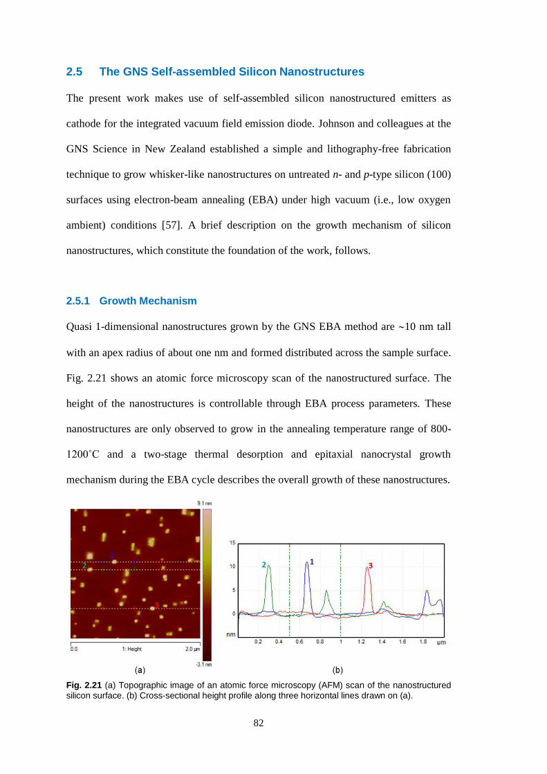
82
2.5 The GNS Self-assembled Silicon Nanostructures
The present work makes use of self-assembled silicon nanostructured emitters as
cathode for the integrated vacuum field emission diode. Johnson and colleagues at the
GNS Science in New Zealand established a simple and lithography-free fabrication
technique to grow whisker-like nanostructures on untreated n- and p-type silicon (100)
surfaces using electron-beam annealing (EBA) under high vacuum (i.e., low oxygen
ambient) conditions [57]. A brief description on the growth mechanism of silicon
nanostructures, which constitute the foundation of the work, follows.
2.5.1 Growth Mechanism
Quasi 1-dimensional nanostructures grown by the GNS EBA method are 10 nm tall
with an apex radius of about one nm and formed distributed across the sample surface.
Fig. 2.21 shows an atomic force microscopy scan of the nanostructured surface. The
height of the nanostructures is controllable through EBA process parameters. These
nanostructures are only observed to grow in the annealing temperature range of 800-
1200˚C and a two-stage thermal desorption and epitaxial nanocrystal growth
mechanism during the EBA cycle describes the overall growth of these nanostructures.
Fig. 2.21 (a) Topographic image of an atomic force microscopy (AFM) scan of the nanostructured silicon surface. (b) Cross-sectional height profile along three horizontal lines drawn on (a).
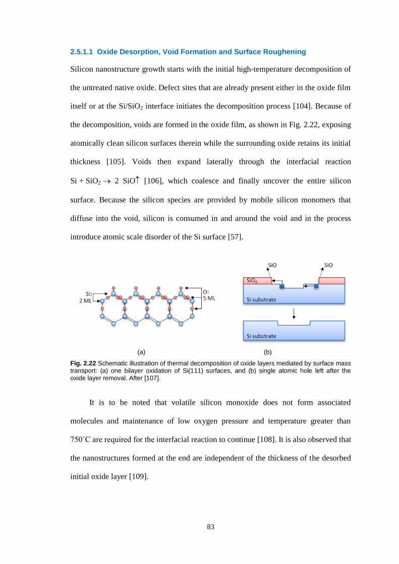
83
2.5.1.1 Oxide Desorption, Void Formation and Surface Roughening
Silicon nanostructure growth starts with the initial high-temperature decomposition of
the untreated native oxide. Defect sites that are already present either in the oxide film
itself or at the Si/SiO2 interface initiates the decomposition process [104]. Because of
the decomposition, voids are formed in the oxide film, as shown in Fig. 2.22, exposing
atomically clean silicon surfaces therein while the surrounding oxide retains its initial
thickness [105]. Voids then expand laterally through the interfacial reaction
Si + SiO2 2 SiO [106], which coalesce and finally uncover the entire silicon
surface. Because the silicon species are provided by mobile silicon monomers that
diffuse into the void, silicon is consumed in and around the void and in the process
introduce atomic scale disorder of the Si surface [57].
(a) (b)
Fig. 2.22 Schematic illustration of thermal decomposition of oxide layers mediated by surface mass transport: (a) one bilayer oxidation of Si(111) surfaces, and (b) single atomic hole left after the oxide layer removal. After [107].
It is to be noted that volatile silicon monoxide does not form associated
molecules and maintenance of low oxygen pressure and temperature greater than
750˚C are required for the interfacial reaction to continue [108]. It is also observed that
the nanostructures formed at the end are independent of the thickness of the desorbed
initial oxide layer [109].

84
2.5.1.2 Epitaxial Nanocrystal Growth
The kinetics of adatom formation, adatom diffusion, and adatom to island attachment
and detachment control the second stage of the nanostructure growth following the
complete oxide desorption. An epitaxial crystal growth model explains additional
surface roughening. The model calls for migration of diffusive adatoms that are
generated both thermally and by electron stimulated desorption process – typically
dimers which are the pairs of top-layer Si atoms on the (100) surface [110] – across
the surface because of the development of strained potential-energy regions from the
surface disorder.
Oshiyama [110] showed that when an adatom was located far (more than 10 Å)
from a step edge, the total energy variation was similar to the flat surface and the
activation energy for diffusion was 0.65 eV. When the adatom approached a step, the
total energy was increased as it passed the top-layer dimer at the step edge. Decrease
in the number of bond formations required for the adatom, caused by missing of one of
the two top-layer dimer atoms at the step edge, Oshiyama argued, was the origin of the
additional activation energies. He calculated the additional activation energy for
adatom diffusion to be 1.1 eV in this case and indicated energetically favourable
bunching of steps to form higher-Miller-indexed facets or nucleating islands once the
flows of the step were pinned.
After the growth of the nucleating islands is terminated and during the anneal
ramp down phase, the island numbers and sizes evolve according to an Ostwald
ripening process [111]. With the presence of step edges of the islands the surface now
is out of equilibrium, and adatoms flow from high curvature steps (i.e., small island) to
low curvature steps (i.e., large island). The result is the further growth of larger islands

85
at the expense of smaller islands that shrink to disappear over time thus reducing both
the number and the height variation of nanostructures at the end.
2.5.2 Role of Electron Beam in Nanostructure Growth
Both oxide desorption and nanocrystal growth may be enhanced by the electron
irradiation [57]. The possible reason for enhanced oxide desorption is due to increased
yield of monomers upon electron irradiation on clean Si surfaces that contribute to the
film desorption in addition to the thermally generated ones. Nakayama and Weaver
[112] showed that exposure produced dimer vacancies thro ugh a combination of atom
desorption and atom transfer processes and related these structural changes to inelastic
cascade scattering. Scattering excites electrons into unstable antibonding states, where
an increased nuclear separation would lower total energy. This transfer of energy from
electronic to nuclear system through relaxation via nuclear motion results in bond
breaking [113] and consequent removal of one atom from a dimer. The event is
followed by escape of the now unpaired atom of the original dimer onto the terrace
(Fig. 2.23).
Fig. 2.23 Electron-stimulated surface modification. The top panel shows potential energy curves for the ground (bonding) state and an unstable repulsive (antibonding) state. The lower panel depicts multiple inelastic scatterings for electrons incident on clean surface [113].

86
As for their proposal that electron irradiation enhances the nanocrystal growth,
Johnson et al. [57] suggested that the process will in general modify the reaction
kinetics and in particular increase the island detachment and adatom formation rates.
2.6 From Field Emitters to Field Emission Devices
The field emitter fabrication processes, as some described in Section 2.4, can be
utilized further to fabricate field emission devices both as ungated diodes and gated
triodes. Since the present work reports the fabrication and characterization of field
emission diodes, the discussion in this section is mostly limited to similar device
configurations only. In a field emission diode, which is the basic field emission device
and shown in Fig. 2.24 along with its notational symbol, electrons are extracted from
the emitter (cathode) and collected in the collector (anode) under a strong electric field
developed by applying voltages between the collector and emitter.
(a) (b)
Fig. 2.24 (a) Schematic structure of a field emission diode, and (b) its circuit symbol. d is the separation between the anode and cathode.
It is to be noted that the current density JFN and the electric field F used in the
Fowler-Nordheim tunnelling Eq. 2.18 are practically inaccessible since the actual
emitting area and the local electric field are unknown. The diode structure provides a
way to measure these quantities through accessible parameters of applied voltage V

87
between the electrodes and current IFN through the electrodes. IFN and V are related to
JFN and F by
(2.30)
and
(2.26)
where A is the emitting surface area in cm2 and the field conversion factor in cm
-1
as discussed in Section 2.3.1. Substituting relations (2.30) and (2.26) in Eq. (2.18), the
Fowler-Nordheim equation can be written in terms of I as a function of the potential
difference V as follows:
(
) (2.31)
Eq. 2.31 will be used exclusively throughout the rest of the work to represent
Fowler-Nordheim field emission current in self-assembled silicon nanostructure field
emission diode.
2.6.1 Silicon Field Emission Diodes
Spindt-type cathodes remain the reference structures for any field emission diode. The
processing sequence of Spindt emitter was shown in Fig. 2.13. Myers and co-workers
[114] used electron beam evaporated silicon instead of molybdenum to fabricate field
emitter arrays that exhibited diode characteristics and Fowler–Nordheim emission
behaviour with turn‐on voltages of ∼80 V. Emitter tip radius was calculated from the
slope of the Fowler–Nordheim plot to be in the range of 10-12 nm.
Hunt, Trujillo, and Orvis [115] fabricated wet chemically etched silicon cold-
cathode diodes and measured field emission current from a 50 50 arrays of such

88
diode structure (Fig. 2.25). In addition to KOH-etched and HF-HNO3-etched cathode
tips, results from tips sharpened by low-temperature oxidation followed by HF etch
were also reported. The measured and reproducible currents followed the Fowler-
Nordheim characteristic with a turn-on voltage of about 4 V (Fig. 2.25(b)) for an
anode-cathode separation of 920 nm. The oxidation-sharpening technique has been
shown to produce tips with a radius of the order of 1 nm [116].
(a)
(b) (c)
Fig. 2.25 (a) Cross-section schematic diagram of the diode measurement structure. Arrays
contained 50 50 tips spaced on 20 m centres. (b) I-V, and (c) Fowler-Nordheim (F-N) plots of
room-temperature measurements made in sharpened tip diodes. represents HF-HNO3-etched, and KOH-etched tips. [115]
Lu et al. [117] reported atmospheric-pressure operation of a field emission diode
based on self-assembled silicon nanostructures fabricated on n-type (100) silicon
substrates using electron beam annealing. Cathodes of these devices were separated
from an aluminium anode by a 1 m thick photoresist spacer. The current versus

89
applied electric field characteristics and Fowler-Nordheim plots are shown in
Fig. 2.26. Saturation region at high field where I-E characteristics departed from
Fowler-Nordheim tunneling was reported. It was argued that though more studies were
required, a space-charge limited condition best described the saturation behaviour.
(a) (b)
Fig. 2.26 (a) I-E characteristics of self-assembled silicon nanostructure field emission diode shown for five consecutive sweeps of the anode voltage. I-E characteristics of the same structure with unstructured cathode in shown in the inset. (b) Corresponding Fowler-Nordheim plots.
2.6.2 Carbon Nanotubes Field Emission Diodes
Attempts were also made to integrate carbon nanotubes in building vacuum
microelectronic devices. Wong et al. [118] presented a novel approach to fabricate
CNT lateral field emission devices. Selective growth of CNTs near the sharp tip
region was achieved by a two-step microwave plasma-enhanced chemical vapour
deposition (MPECVD) process that involved a pre-growth hydrogen plasma treatment.
The schematic process flow and I-V characteristics are shown in Fig. 2.27.
Subramanium and coworkers [119] fabricated and examined lateral field
emission diodes using the same MPECVD to grow nanodiamond films with grain size
as small as 5 nm to be patterned as finger-like emitters by conventional

90
photolithography (Fig. 2.28(a)). The I-V characteristic of the device is shown in Fig.
2.28(b).
(a) (b)
Fig. 2.27 (a) Schematic diagram of the single-mask microfabrication process of the lateral CNT field emission device. (b) Plot for the anode current vs. the applied field with F-N plot of the corresponding emitter data as inset. [118]
(a) (b)
Fig. 2.28 (a) SEM micrograph and (b) field emission characteristics of the 6-finger lateral diode. [119]

91
The fabrication of CMOS process compatible integrated field emission diode
using self-assembled silicon nanostructures is reported in Chapter 5. Characterization
of the same devices was carried out through electrical measurements and results are
reported and analysed in Chapter 6 along with comparisons with devices discussed in
this section.
2.7 Summary
In this chapter, the fundamental physics of field emission from metals and
semiconductors and various approaches to fabricate field emitters and field emission
devices were discussed. Field penetration and image charge effects for semiconductors
were described but later simplified for moderately low doped silicon samples so that
Eq. 2.31 represents for all practical purposes the Fowler-Nordheim tunnelling equation
for the fabricated device. Effects of emitter shapes on local field enhancement were
reviewed and the concept of field conversion factor and field enhancement factor were
introduced. Introductory simulation results on field enhancement were reported which
set the stage for Chapter 7 where models for the self-assembled silicon nanostructures
as well as field emission diodes will be made and field factor will be determined and
compared with conductive atomic force microscopy and device characterization results
respectively from Chapters 4 and 6.
Chapter 3 next describes the experimental methods and techniques used in the
fabrication and characterization of the field emission devices using electron beam
annealed self-assembled silicon nanostructure emitting sources.

92
93
Chapter 3
PROCESS AND CHARACTERIZATION
– METHODS AND TOOLS
Fabrication of the integrated field-emission diodes using self-assembled silicon
nanostructures consisted of several standard complementary metal-oxide-
semiconductor (CMOS) process steps. The sequence of these steps is shown in
Fig. 3.1 as a series of schematic cross-sections, each depicting the end of a major step
or multiple steps for the completed device. A thorough understanding of these major
process-steps, namely, oxidation, lithography, etching, ion implantation, metallization,
and e-beam annealing and expertise on the respective tools are necessary to develop a
process recipe for the fabrication of a device that performs according to the designed
criteria and for its reliable reproductions.
Also essential in between these process steps is the characterization of the
resulting structures to ensure that the fabrication is proceeding according to the
intended design. Among these in-process characterizations, layer thickness and surface
roughness measurements played vital roles for the device fabricated in this research.
Electrical characterizations of the nanostructured silicon surface and of the completed
device were also two of the major objectives of this research.

94
Fig. 3.1 Major fabrication process steps for field-emission diode based on silicon nanostructures.
This chapter describes the methods and apparatuses that were employed in the
fabrication and characterization of the diodes fabricated and characterized in this
research. The description includes fabrication techniques and tools for oxidation,
lithography, etching, ion implantation, metallization, and e-beam annealing.
Characterization methods and tools for surface profilometry, atomic force microscopy
(AFM), scanning electron microscopy (SEM), and I-V spectroscopy were also
discussed.
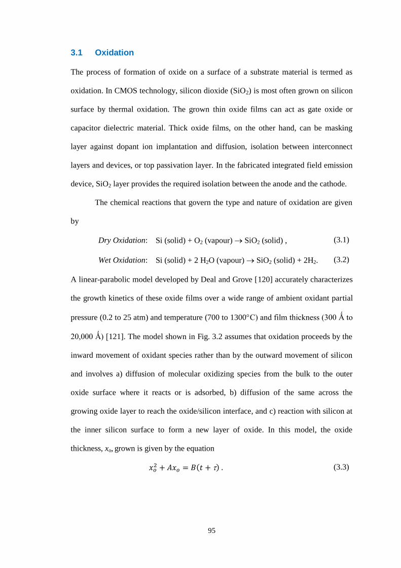
95
3.1 Oxidation
The process of formation of oxide on a surface of a substrate material is termed as
oxidation. In CMOS technology, silicon dioxide (SiO2) is most often grown on silicon
surface by thermal oxidation. The grown thin oxide films can act as gate oxide or
capacitor dielectric material. Thick oxide films, on the other hand, can be masking
layer against dopant ion implantation and diffusion, isolation between interconnect
layers and devices, or top passivation layer. In the fabricated integrated field emission
device, SiO2 layer provides the required isolation between the anode and the cathode.
The chemical reactions that govern the type and nature of oxidation are given
by
Dry Oxidation: Si (solid) + O2 (vapour) SiO2 (solid) , (3.1)
Wet Oxidation: Si (solid) + 2 H2O (vapour) SiO2 (solid) + 2H2. (3.2)
A linear-parabolic model developed by Deal and Grove [120] accurately characterizes
the growth kinetics of these oxide films over a wide range of ambient oxidant partial
pressure (0.2 to 25 atm) and temperature (700 to 1300C) and film thickness (300 Ǻ to
20,000 Ǻ) [121]. The model shown in Fig. 3.2 assumes that oxidation proceeds by the
inward movement of oxidant species rather than by the outward movement of silicon
and involves a) diffusion of molecular oxidizing species from the bulk to the outer
oxide surface where it reacts or is adsorbed, b) diffusion of the same across the
growing oxide layer to reach the oxide/silicon interface, and c) reaction with silicon at
the inner silicon surface to form a new layer of oxide. In this model, the oxide
thickness, xo, grown is given by the equation
( ) (3.3)

96
Fig. 3.2 Oxidation model after Deal and Grove [120].
B/A in Eq. 3.3 is referred to as the linear rate constant of a short term reaction-
controlled and B as the parabolic rate constant of a long term diffusion-controlled
oxidation regime. is a shift in time to account for the presence of the initial oxide
layer of thickness xi, the effect of which is as if the oxidation had started at a time
and at the thickness of the oxide was xi. Good experimental fit of these constants
for different temperatures are reported by Deal and Grove and are given in Tables 3-1
and 3-2.
Table 3-1 Rate constants for oxidation of silicon in wet oxygen (95C H2O).
Oxidation
Temperature (C) A () B (
2/h) B/A (/h) r(h)
1200 0.05 0.720 14.40 0
1100 0.11 0.510 4.64 0
1000 0.226 0.287 1.27 0
920 0.50 0.203 0.406 0

97
Table 3-2 Rate constants for oxidation of silicon in dry oxygen.
Oxidation
Temperature (C) A () B (
2/h) B/A (/h) r(h)
1200 0.040 0.045 1.12 0.027
1100 0.090 0.027 0.30 0.076
1000 0.165 0.0117 0.071 0.37
920 0.235 0.0049 0.0208 1.40
800 0.370 0.0011 0.0030 9.0
700 … … 0.00026 81.0
Thermal oxidation rates of silicon depends on parameters such as
a) crystallographic orientation of the substrate [122], e.g., at different temperatures
<111> silicon exhibits B/A values about 1.68 times those of <100> silicon [123],
b) substrate doping level with higher rates at higher impurity concentration which
raises point defects concentration that may provide more reaction sites to covert Si to
SiO2 [124], and c) growth pressure with rates linearly proportional to the pressure
[125]. In addition, presence of chlorine or other halogen impurities, plasma, and
photon flux during growth enhance thermal oxidation rate [126].
3.1.1 Oxidation Apparatus
A schematic diagram of a thermal oxidation system is shown in Fig. 3.3(a). The same
system is used in diffusion and annealing, where the process gas determines the
eventual process type. The system contains resistance-heating elements, a cylindrical
fused-quartz tube, a source cabinet, and a temperature control system. Wire resistance
heaters surround outside and are spaced along the tube length to provide three heating
zones. Silicon wafers to be oxidised are held vertically in a slotted quartz boat and put
into the tube from the loading end. Process gas enters through one end of the tube and
exits through the other. Distribution of process gases such as O2, H2, N2, HCl, and Ar
along with O2 saturated steam are maintained at the source cabinet, while data from

98
thermocouples control the power of the heater windings to maintain uniform oxidation
temperature. Additionally, a thermal oxidation system may contain a clean
environment load station and an automatic loading system to push and pull wafer boats
at controlled rate. Fig. 3.3(b) shows the oxidation furnace available at the University
of Canterbury.
(a)
(b)
Fig. 3.3 (a) Schematic cross section of a resistance-heated oxidation furnace [127]. (b) Oxidation furnace at the University of Canterbury.
3.1.2 Oxide Thickness Measurement
The thickness of a grown oxide layer is measured by creating a step in the oxide by
using a mask definition over the oxide and subsequent hydrofluoric acid (HF) etch to

99
remove the oxide layer completely in the defined area. When masking layer is
removed the step height of the etched area would nearly equal the oxide layer
thickness. The step height can be measured using a surface profilometer for thick
oxide layers or for thin oxide layers by atomic force microscopy. Alternatively, the
oxide layer thickness can be directly measured using an ellipsometer.
3.2 Optical Lithography
Lithography is a process in which radiation is applied to transfer a 2-dimensional
pattern onto a radiation-sensitive resist that from then on is employed to create
intended structure in the underlying substrate or material layer. Since multiple patterns
are to be formed in the substrate and in other layers that a final device may have,
lithographic steps are used repeatedly in semiconductor processing. The minimum
feature size, i.e., linewidth or space in a pattern, which can be adequately transferred
or resolved, is known as the resolution of the lithographic system. Registration is a
measure of scale to which the pattern being transferred “fits” or “aligns” with respect
to a preceding transferred pattern.
From among many methods as shown in Fig. 3.4 that can be used in
lithography, mask-based optical lithography is used in fabricating the field emission
diode and therefore is discussed in detail here. Optical lithography comprises of a
mask, an ultraviolet light source, and photosensitive resist, called photoresist, on the
substrate or the layer to be patterned. Patterns are transferred from the mask onto the
photoresist upon ultraviolet radiation exposure and subsequent photoresist
development. An example of the optical lithography pattern transfer on oxide layer
where etching (discussed in Section 3.3) of oxide followed the photoresist
development is shown in Fig. 3.5.
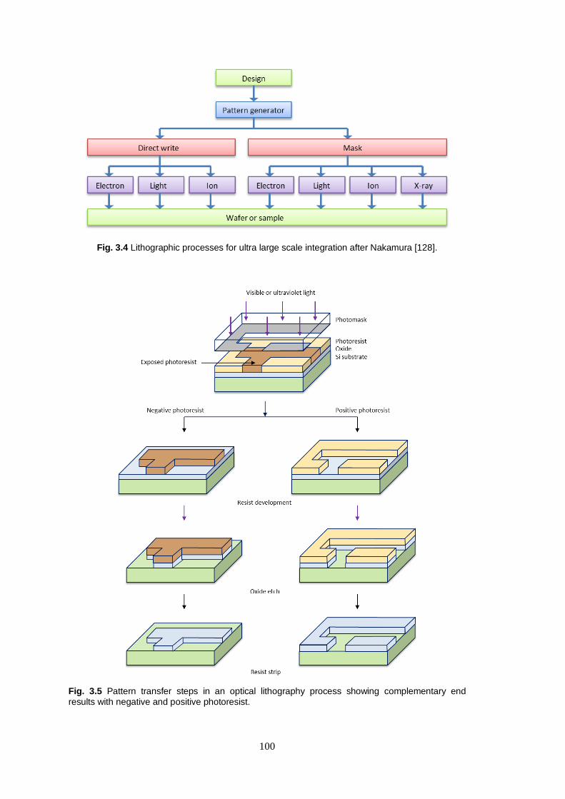
100
Fig. 3.4 Lithographic processes for ultra large scale integration after Nakamura [128].
Fig. 3.5 Pattern transfer steps in an optical lithography process showing complementary end results with negative and positive photoresist.
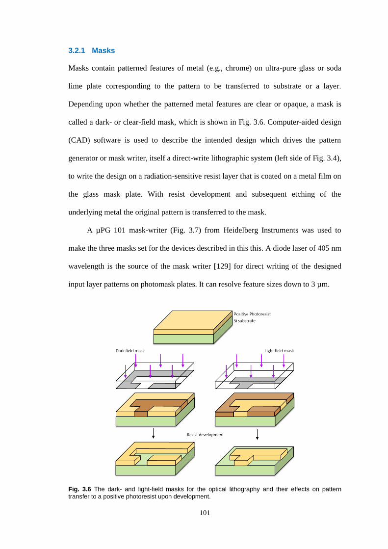
101
3.2.1 Masks
Masks contain patterned features of metal (e.g., chrome) on ultra-pure glass or soda
lime plate corresponding to the pattern to be transferred to substrate or a layer.
Depending upon whether the patterned metal features are clear or opaque, a mask is
called a dark- or clear-field mask, which is shown in Fig. 3.6. Computer-aided design
(CAD) software is used to describe the intended design which drives the pattern
generator or mask writer, itself a direct-write lithographic system (left side of Fig. 3.4),
to write the design on a radiation-sensitive resist layer that is coated on a metal film on
the glass mask plate. With resist development and subsequent etching of the
underlying metal the original pattern is transferred to the mask.
A µPG 101 mask-writer (Fig. 3.7) from Heidelberg Instruments was used to
make the three masks set for the devices described in this this. A diode laser of 405 nm
wavelength is the source of the mask writer [129] for direct writing of the designed
input layer patterns on photomask plates. It can resolve feature sizes down to 3 µm.
Fig. 3.6 The dark- and light-field masks for the optical lithography and their effects on pattern transfer to a positive photoresist upon development.

102
Fig. 3.7 Heidelberg Instruments’ µPG 101 mask-writer.
3.2.2 Photoresists
As seen in Fig. 3.5, the actual transferred pattern depends on the type of photoresist –
positive or negative photoresist. Upon exposure to light, positive photoresists become
more soluble and negative photoresists becomes less soluble in a resist developer
solution.
Negative photoresists consist of film forming polymer and a photoactive
compound. The photoactive compound upon exposure initiates a polymer cross-
linking process. The cross-linked polymer has a higher molecular weight and it
becomes insoluble to an organic developer solution [130]. After photoresist
development, the unexposed areas are removed and a reverse or “negative” pattern is
transferred to the photoresist. The exposed photoresist swells during development
distorting the pattern features and limits resolution to 2 to 3 times the initial film
thickness [131]. For this reason though negative photoresists found fewer usages in
modern microelectronic processing. However, newer epoxy-based SU-8 negative

103
photoresists are now being routinely used in microfluidics and micro-
electromechanical systems fabrication.
A positive photoresist contains a photoactive compound and a resin dissolved
in an organic solvent. The photoactive compound is a dissolution inhibitor and is
destroyed in areas exposed under light and resin in the area becomes more soluble in
an aqueous developer solution and therefore, are removed during the photoresist
development process. As a result an exact or “positive” pattern is left of the
photoresist. Commercially available Clariant Corporation’s positive photoresist
AZ1815 is used in this research. MIF 300 from the same company is used as the
photoresist developer solution.
3.2.3 Exposure Techniques and Tools
Patterns can be transferred by three different exposure methods; namely, contact,
proximity, and projection printing. Schematics of these methods are shown in
Fig. 3.8.
Contact printing (Fig. 3.8(a)), is the earliest lithography technique where
photoresist-covered sample and mask are kept in complete physical contact during
exposure. This arrangement yields the best optical resolution. 0.4 m linewidth in a
0.98 m thick resist was resolved as early as in 1973 using contact lithography [132].
However, the method generates defects in the mask from repeated mask-to-
photoresist-covered-wafer contacts. As a result masks are to be discarded after a short
period of use and as such the method is mostly abandoned in commercial
microelectronic manufacturing.
In proximity printing (Fig. 3.8(b)), the mask and photoresist-covered wafer are
placed very close to one another but without a contact during exposure. The gap

104
maintained between mask and wafer is typically in the range of 30 to 50 m. The
method avoids the problem of mask defect generation from mask-to-wafer contacts as
in the case of contact printing and provides masks a longer life. However, it introduces
degradation of resolution from diffraction [133].
(a) (b) (c)
Fig. 3.8 Schematic diagrams of optical (a) contact, (b) proximity, and (c) projection lithographic techniques.
In projection printing (Fig. 3.8(c)), both high resolution and lower mask defect
generation are achieved. In this technique, mask is held between condenser and a
second set of lenses called the projector or objective, which refocuses the diffracted
light onto the resist-covered wafer. The resolution of the projection lithography is
limited by the projector’s ability to collect and reimage the diffracted light, i.e., by
numerical aperture of the system.
Exposure tools, called mask aligners, are used for imaging the mask patterns
onto the photoresist-coated samples using any of the three radiation exposure
techniques. A mask aligner consists of a light source that exposes the photoresist, an
optical subsystem that focuses the mask patterns onto the photoresist-covered sample
or wafer surface, a movable stage that holds the wafer to be exposed, and an alignment
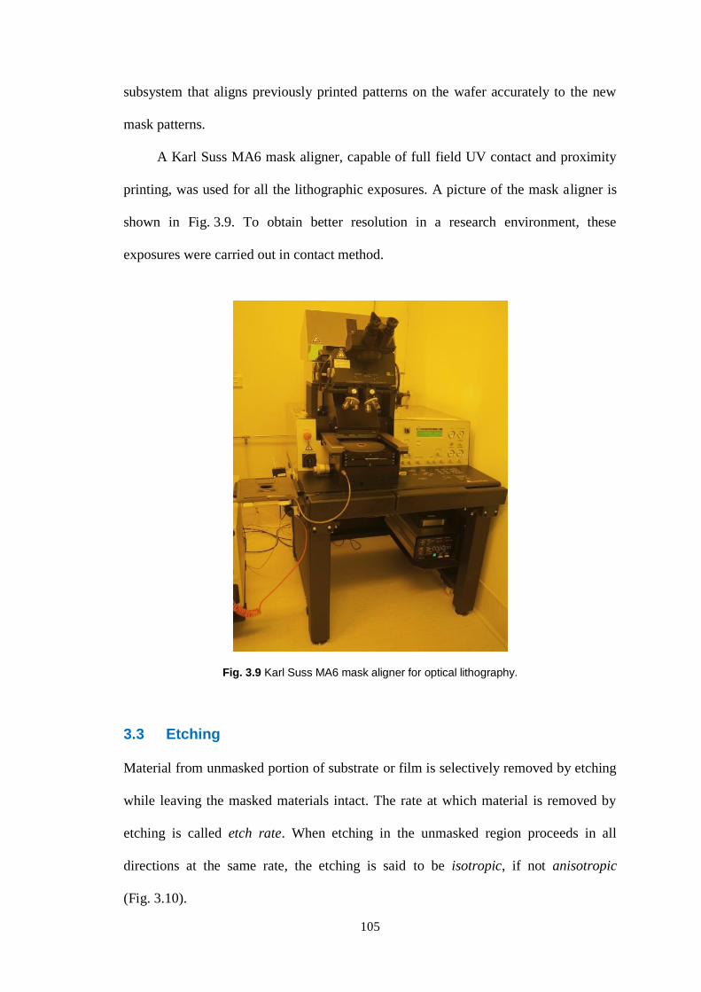
105
subsystem that aligns previously printed patterns on the wafer accurately to the new
mask patterns.
A Karl Suss MA6 mask aligner, capable of full field UV contact and proximity
printing, was used for all the lithographic exposures. A picture of the mask aligner is
shown in Fig. 3.9. To obtain better resolution in a research environment, these
exposures were carried out in contact method.
Fig. 3.9 Karl Suss MA6 mask aligner for optical lithography.
3.3 Etching
Material from unmasked portion of substrate or film is selectively removed by etching
while leaving the masked materials intact. The rate at which material is removed by
etching is called etch rate. When etching in the unmasked region proceeds in all
directions at the same rate, the etching is said to be isotropic, if not anisotropic
(Fig. 3.10).
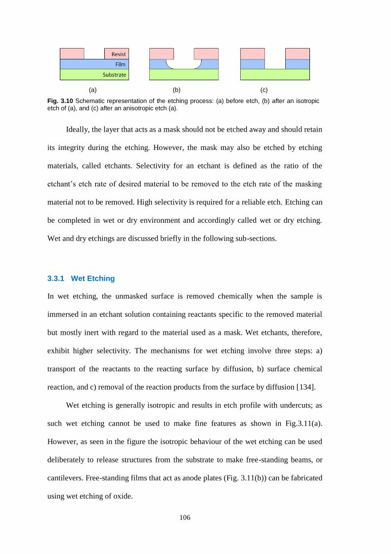
106
(a) (b) (c)
Fig. 3.10 Schematic representation of the etching process: (a) before etch, (b) after an isotropic etch of (a), and (c) after an anisotropic etch (a).
Ideally, the layer that acts as a mask should not be etched away and should retain
its integrity during the etching. However, the mask may also be etched by etching
materials, called etchants. Selectivity for an etchant is defined as the ratio of the
etchant’s etch rate of desired material to be removed to the etch rate of the masking
material not to be removed. High selectivity is required for a reliable etch. Etching can
be completed in wet or dry environment and accordingly called wet or dry etching.
Wet and dry etchings are discussed briefly in the following sub-sections.
3.3.1 Wet Etching
In wet etching, the unmasked surface is removed chemically when the sample is
immersed in an etchant solution containing reactants specific to the removed material
but mostly inert with regard to the material used as a mask. Wet etchants, therefore,
exhibit higher selectivity. The mechanisms for wet etching involve three steps: a)
transport of the reactants to the reacting surface by diffusion, b) surface chemical
reaction, and c) removal of the reaction products from the surface by diffusion [134].
Wet etching is generally isotropic and results in etch profile with undercuts; as
such wet etching cannot be used to make fine features as shown in Fig.3.11(a).
However, as seen in the figure the isotropic behaviour of the wet etching can be used
deliberately to release structures from the substrate to make free-standing beams, or
cantilevers. Free-standing films that act as anode plates (Fig. 3.11(b)) can be fabricated
using wet etching of oxide.

107
(a)
(b)
Fig. 3.11 Undercut in wet etching: (a) wide line underneath the top layer narrows and narrow line disappears to completely release the top layer [135]; and (b) top layer hole definition by anisotropic dry etching and subsequent selective isotropic wet etching of oxide release the top layer [136].
Hydrofluoric acid (HF) based etchants are used generally for wet etching silicon
dioxide. For pure HF etching, the overall reaction is [137]
( ) . (3.4)
In this research buffered HF (BHF), also known as buffered oxide etch (BOE), a
mixture of 40 g NH4F in 10 ml 49% HF with 60 ml H2O, is used in room temperature
for the purpose of etching SiO2. Kikuyama et al. [138] describe the reaction of in
BHF by
( ) . (3.5)
They report ions are dominant etching species for , not the ions as
previously thought, and the details of the etching steps are:
.
.
.
.
( ) . (3.6)

108
Buffering with NH4F helps keep the pH and therefore the concentrations of HF and
HF2– constant. This stabilizes the etch rate, which would otherwise have been
decreased as HF and HF2– are consumed during etching. HF-based solutions are highly
corrosive and must be handled by containers and tools made from polypropylene,
high-density polyethylene (HDPE), polytetrafluo-roethylene (PTFE), polyvinylidene
fluoride (PVDF), or similar material as the solutions also etch glass container and
tools [137].
3.3.2 Dry Etching
Various dry etching processes with their basic mechanism, chamber pressure and other
characteristics are recorded in Table 3-3. From among these processes, Reactive Ion
Etching (RIE) is used in this research to etch tungsten (W) to define cathode and anode
plates as well as to open cathode areas under anode plate for nanostructure growth.
The RIE process is briefly discussed in this section.
Table 3-3 The dry-etching spectrum.
Dry etching
process
Chamber
pressure
Basic
mechanism
Excitation
energy Characteristics
Sputtering and ion milling
< 10 mTorr
Physical
momentum
transfer
High
High anisotropy etch
Poor selectivity Prone to radiation
damage
Reactive ion
etching
10 to 100
mTorr
Physical and
chemical Medium
Anisotropic
Selective
Radiation damage
possible
Plasma
etching
> 100
mTorr Chemical Low
Isotropic
More selective
Less prone to radiation
damage
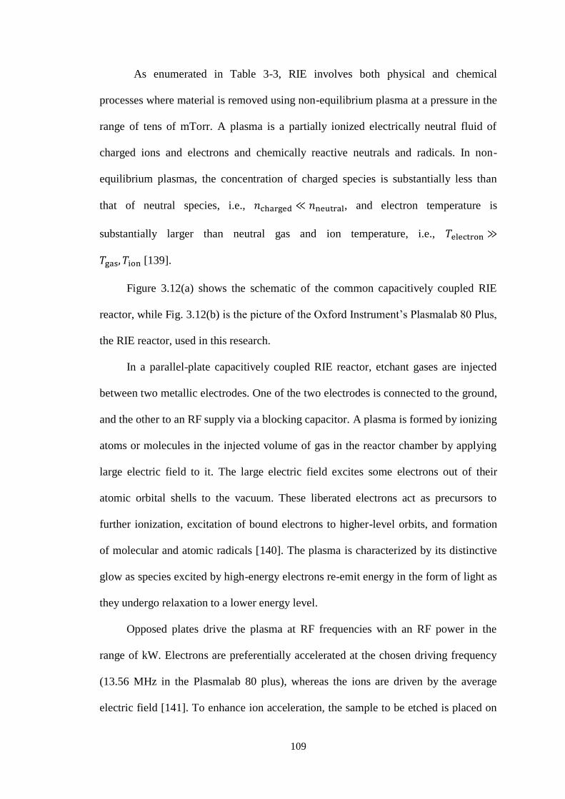
109
As enumerated in Table 3-3, RIE involves both physical and chemical
processes where material is removed using non-equilibrium plasma at a pressure in the
range of tens of mTorr. A plasma is a partially ionized electrically neutral fluid of
charged ions and electrons and chemically reactive neutrals and radicals. In non-
equilibrium plasmas, the concentration of charged species is substantially less than
that of neutral species, i.e., , and electron temperature is
substantially larger than neutral gas and ion temperature, i.e.,
[139].
Figure 3.12(a) shows the schematic of the common capacitively coupled RIE
reactor, while Fig. 3.12(b) is the picture of the Oxford Instrument’s Plasmalab 80 Plus,
the RIE reactor, used in this research.
In a parallel-plate capacitively coupled RIE reactor, etchant gases are injected
between two metallic electrodes. One of the two electrodes is connected to the ground,
and the other to an RF supply via a blocking capacitor. A plasma is formed by ionizing
atoms or molecules in the injected volume of gas in the reactor chamber by applying
large electric field to it. The large electric field excites some electrons out of their
atomic orbital shells to the vacuum. These liberated electrons act as precursors to
further ionization, excitation of bound electrons to higher-level orbits, and formation
of molecular and atomic radicals [140]. The plasma is characterized by its distinctive
glow as species excited by high-energy electrons re-emit energy in the form of light as
they undergo relaxation to a lower energy level.
Opposed plates drive the plasma at RF frequencies with an RF power in the
range of kW. Electrons are preferentially accelerated at the chosen driving frequency
(13.56 MHz in the Plasmalab 80 plus), whereas the ions are driven by the average
electric field [141]. To enhance ion acceleration, the sample to be etched is placed on

110
the powered electrode. The sample in plasma is bombarded with both electrons and
positive ions. At the beginning, the sample becomes negatively charged as it collects
more electrons because of their higher mobility. Later electrons start to repel from the
sample surface and positive ions are attracted toward it and at some negative potential,
the electron and ion fluxes become equal. The sample at this stage remains at the
floating potential which is less than the plasma bulk potential.
(a)
(b)
Fig. 3.12 (a) Schematic of a parallel-plate capacitively coupled reactive ion etching reactor. (b) Oxford Instrument Plasmalab etcher shown with etchant gas arrangement.

111
The regions near the sample and the electrodes contain relatively few energetic
electrons and lack re-emission of light from electron relaxation. The dark space that
results in those regions is known as the plasma sheath. Positive ions accelerate across
the sheath due to the potential difference between the plasma bulk and floating sample
and bombard the sample surface normally. Since the sample is connected to an
oscillating power supply through the powered electrode, the ion energy is further
increased. Due to collisions with the ions, neutral radicals in plasma can also strike the
sample surface and enhance the etch rate.
Anisotropy in RIE involves both enhancement of the etching rate in the vertical
direction from highly directional ion bombardment and retardation of the etching rate
in the horizontal direction through the formation of passivating films on sidewall. As
the Figure 3.13 shows schematically, the passivating films are formed as the etching
proceeds with little ion bombardment on the sidewalls.
Fig. 3.13 Schematic diagram of an anisotropic reactive ion etching showing the formation of passivating sidewall film. Neutral radical strikes are not shown [142].
The electron mean free path limits the operating pressure. If the pressure is
lowered near the level at which the electron mean free path approaches the gap

112
between the electrodes, which is several centimetres, the plasma is no longer self-
sustaining [141].
3.4 Ion Implantation
Energetic dopant ions are irradiated in a controlled and reproducible manner on
selected areas of a substrate surface and introduced into regions underneath the same
by ion implantation. The details on ion implantation can be found in references [143,
144, 145, 146] and only its basic concepts are discussed here. In this work ion
implantation has been carried out to form highly conductive substrate regions that
yield good ohmic cathode contacts. The regions where ion implantation is not desired
are masked with photoresist layer thick enough to stop irradiating ions from reaching
the substrate surface.
3.4.1 Ion Implantation System
A simplified schematic of a medium-current ion implanter is shown in Fig. 3.14. At
the beginning of the ion implantation process, gaseous dopant atoms are ionised into
desired implant species along with other unwanted species and contaminants inside an
ion source of an ion implanter. These ions exit the ion source through a slit under
extraction voltage of around 20 kV forming an ion beam into an analyzer. Inside the
analyzer, ions are deflected by a magnetic field perpendicular to the beam and
separated according to their mass: heavier ions deflect less, lighter ions more. Only the
ions of desired species are allowed to travel into an acceleration tube from high
voltage end to ground and accelerated to the chosen implantation energy. Lenses and
apertures in the system ensure a well-focussed and collimated beam.

113
Some ions may combine with thermal electrons and thus undesirable neutral
atoms may reappear in the beam at this stage. To trap neutrals a bend is provided
where parallel electrostatic plates deflect the ion beam slightly off the accelerator tube
axis. Neutrals are not deflected and neutral beam follows the straight path along the
accelerator tube axis and ends at a beam stop.
Fig. 3.14 Schematic of a low energy ion implanter that utilizes a mass-analysed beam.
At the end station of the ion implanter, the ion beam is further deflected using
sets of horizontal and vertical electrostatic deflection plates to scan and irradiate a
wafer or a sample. The pressure of the entire system is maintained below 10-6
torr to
minimize ion scattering.
An ion implanter at GNS Science in Wellington, New Zealand (Fig. 3.15) was
used for the present work. The ion implanter can implant any material with elements
and isotopes at energies from 5 to 100 keV typically on a 10 mm10 mm target.

114
Fig. 3.15 Low energy ion implanter at GNS Science used for doping and surface modification. Courtesy: GNS.
3.4.2 Implantation Dose and Impurity Concentration
The implantation dose, in atoms/cm2 is related to beam current I in amperes, area
scanned A in cm2, and implantation duration t in sec by
(3.12)
where q is the charge per ion and equal to an electronic charge, 1.610–19
C.
Depending upon the implant species, energy, and model of an implanter, the beam
current typically ranges between 10 A to 30 mA and implant dose 1011
atoms/cm2
to
1016
atoms/cm2 [147].
The implanted impurity concentration (profile) along the incident direction can
be approximated by a Gaussian distribution function n(x) with standard deviation Rp.
( )
√ [
( )
] (3.13)
where Rp is the projected range and Rp the projected struggle of the implanted species
illustrated in Fig. 3.16.

115
Fig. 3.16 Schematic view of ion range. (a) The total path length R is longer than the projected range Rp. (b) The stopped atom distribution is two dimensional Gaussian [144].
3.4.3 Advantages of Ion Implantation
Accurate projected range can be realized by adjusting the initial energy of the dopant
ions by reducing or increasing the acceleration voltage. Precise implantation dose can
be reached by adjusting the value of the beam current. Projected range and
implantation dose, therefore, can be maintained electrically which provides well-
defined process controllability and reproducibility. In addition, since ion implantation
is a low-temperature process, existing impurity profile is not affected by ion
implantation and photoresist can be generally used as implant mask layers.
3.4.4 Implantation Damage
In case of nuclear collisions, as energetic ions travel through the substrate lattice and
lose energy, host substrate atoms can be displaced if transferred energy is greater than
the binding energy of the lattice atoms. Depending on the amount of transferred
energy, further displacements of lattice atoms are possible from the scattering events
116
by displaced but energetic secondary recoiled lattice atoms as they lose energy through
nuclear collisions to come to a complete stop. Each displacement of a lattice atom by
either a primary ion or a secondary recoiled lattice atom produces point defect called
Frenkel defect.
Other implant damages include defects such as vacancies, divacancies, and
interstitials [148] that introduce disorder in the substrate crystal lattice. The dopants
after the implantation are mostly placed as interstitials and form no bonds with
neighbouring atoms to provide free charge carriers and therefore are electrically
inactive.
3.4.5 Annealing
Electrically, regions after implantation with damaged lattice and interstitial ions
become more resistive as carrier mobility in these regions degrades [149] and deep-
level electron and hole traps now present there capture carriers [144]. To repair the
crystal lattice damage and electrical activation of dopant ions annealing at high
temperature, usually 900C or more, for a short period of time is required. Annealing
energy allows ions to diffuse to substitutional sites, form bonds with neighbouring
atoms, provide free charge carriers for conduction and thus to become electrically
active. Vacancies are also filled up by the displaced atoms resulting in recovery of the
crystal lattice. Electron-Beam Annealing is used in this research for annealing of the
implanted arsenic (As) species in silicon samples and is discussed in detail in
Section 3.6.

117
3.5 Metallization
Thin and conductive metal films provide interconnection between contacts on device
components and from device to the outside world in a standard CMOS process. These
films are deposited primarily by physical vapour deposition (PVD). Thermal
evaporation, e-beam evaporation, direct-current (DC) sputtering, and radio-frequency
(RF) sputtering are the most common forms of PVD. In this research tungsten was
deposited using the DC sputtering technique to form anode plate and also cathode
contact to silicon substrate for the fabricated field-emission device. The DC sputtering
offered highly controlled and uniform deposition of this high-temperature metal. An
Edwards Auto-500 magnetron system (Fig. 3.17(a)) was employed for the purpose.
The schematic diagram of the magnetron system is shown in Fig. 3.17(b).
The sputter deposition involves ejection of a material from a ‘target’ (cathode)
under ion bombardment and deposition of the same onto a ‘substrate’ (anode). The
sputtering process starts with the creation of vacuum to remove impurities from the
chamber inside which the target, biasing electronics, magnet arrangements, and the
sample (substrate) are located. An inert gas (in our case, Ar) is supplied into the
chamber and a plasma is initiated by applying a large voltage across the electrodes. In
DC sputtering the applied bias is maintained in the same direction; whereas, in RF
sputtering the bias sign changes between the electrodes at radio frequency, a process
that resists charge build-up on insulating targets. In eith er case, sputtered or ejected
atoms with sufficient energy travels through the distance in between the electrodes to
deposit on the substrate held at the anode. A detail of the sputtering physics and tools
can be found in [150].

118
(a)
(b)
Fig. 3.17 (a) Edwards Auto-500 magnetron system of the University of Canterbury nanolab. (b) Schematic diagram of a planar magnetron sputtering system.
In magnetron sputtering, the application of a magnetic field from a set of
magnets added behind the target causes the electrons in the plasma to follow the
direction of the magnetic field lines parallel to the surface of the target (Fig. 3. 17(b))
increasing the probability that they collide with neutral species and create ions. This
potentially increases the ion density which in turn increases the rate of ion
bombardment and consequently the deposition. The power of the DC source is the
main parameter that controls the rate and quality of the deposition.
119
3.6 Electron Beam Annealing
Annealing of semiconductor samples using specifically designed electron gun scans
was reported in early 1980s with anneal times ranging from 10−4
sec to a few minutes
which is the lowest limit of a conventional furnace treatment [151]. The method is a
fast isothermal annealing technique where temperature remains uniform throughout a
semiconductor sample. Isothermal heating of the irradiated area is made possible
because of the fast scanning of the electron beam, which ensures that on the average
the same energy is deposited at all points of the scanned field [152]. Annealing times
are set such that they are long enough for the recrystallization of the implanted layer
and the activation of the dopant, but are short enough that diffusion effects are
negligible compared with their extent in furnace annealing [153]. In addition to fast
activation and minimal diffusion of dopants, electron beam interaction with silicon
surface promotes controlled growth of silicon nanostructures [57]. These
nanostructures act as electron emission sites and are grown in the defined cathode area
of the fabricated device.
An electron beam annealer at GNS Science was used in this research. The
system can heat 1010 mm2 samples from 300C up to 1300C within an accuracy of
1C with precise temperature ramp up and down rates of 1 to 100C/s. Up to 20
samples can be loaded in the system chamber for this high vacuum annealing.
Fig. 3.18 shows the schematic diagram of the system.
The beam current of the system from the electron filament is generated by the
bias voltage between the control grid electrode, known as Wehnelt, and the cathode.
External bias is derived by rectifying a high-frequency carrier which is coupled
through a transformer with 20kV isolation. The beam, therefore, with 20 keV of
electron energy and current up to 2 mA, travels through the Wehnelt cyclinder, Einzel

120
lens, x- and y-deflection scanning plates and is focused on the sample surface to a spot
of approximately 1 mm diameter. The beam scans over the 1010 mm2 sample area
with x- and y-sweep frequencies of 1 and 10 kHz respectively.
Fig. 3.18 Schematic of electron beam annealing system. Tsample is the sample temperature as measured by the 2-colour pyrometer, Tradiation is the sample temperature as measured by the thermopile detector and Ie is the current induced by the electron beam measured through the sample [154].
Effective control of the beam current is essential for precise control of
temperature and is done via a thermopile detector which is connected through the
feedback loop to the biasing controller. A pair of two-colour pyrometers which face
the front and back of the sample surfaces measures the true temperature.
-
+ U
Filament
UWehnelt
Uacceleration
Tsample
Tradiation
2-colour pyrometer
Thermopile
detector
Sample
X-Y scanner
Einzel lens
Wehnelt cylinder
Filament
PC
I/O Interface
-
+
+
-
Sample wheel
20kV Isolation
Transformer
Ie

121
3.7 Atomic Force Microscopy
Atomic force microscopy (AFM) was employed for topographical and electrical
surface characterization of silicon nanostructures in this research. Dimension 3100
(Fig. 3.19), a AFM system from Bruker Corporation (previously Digital Instrument),
was used exclusively for the purpose. Binnig, Quate, and Gerber invented Atomic
Force Microscopy (AFM), also called Scanning Force Microscopy (SFM), in 1986
[22] and made nanometre scale 3-D imaging of almost any type of conducting,
semiconducting, or insulating surfaces a reality. Unlike using a beam of light or
electrons as in optical or electron microscopy, or using tunnelling current sensing as in
Scanning Tunnelling Microscopy (STM), AFM uses a fine probing tip to scan over a
surface or being scanned under by a surface and construct the surface topography by
sensing the force between the surface and the tip. AFM imaging, therefore, is no
longer limited to wavelength of light and electrons, or substrate type and lateral (x and
y) features of 2–10 nm on any material surface can be routinely resolved, with a
vertical (z) resolution as good as 0.1 nm [155].
(a) (b)
Fig. 3.19 (a) Picture of the Dimension 3100 AFM. (b) Schematic diagram showing the elements in the AFM head.

122
The basic AFM principle and modes of operations including conductive and lift
mode AFM techniques that are available in DI 3100 and are used in the present
research (Chapter 4) are also discussed briefly in the following sections. Detail
information on this AFM system can be found in [156] and [157].
3.7.1 AFM Basic Principle
The probing tip of an atomic force microscope is mounted on the free end of a very
light and very flexible cantilever. During a scan, the cantilever bends in response to
the repulsive or attractive force between the sample surface and the tip. In any case,
the bending of the cantilever is measured using a beam-deflection method introduced
by Meyer and Amer [158] and shown in Fig. 3.20. In this method, laser light from a
solid state laser diode is reflected from the backside of the cantilever and captured by a
split-photodiode (closely spaced photodiodes A and B) position-sensitive detector
(PSD) whose outputs are fed to a differential amplifier that produces an output signal
equal to the difference between the photodiode signals (A-B) normalized by their sum
(A+B). When cantilever bends, its angular displacement causes one photodiode to
collect more light than the other photodiode, producing an output signal proportional
to the deflection of the cantilever.
Fig. 3.20 Schematic diagram shows the beam deflection detection system in an AFM [157].
Solid state laser diode
Cantilever and tip
Split photodiode detector
Output:
A
B A – B A + B
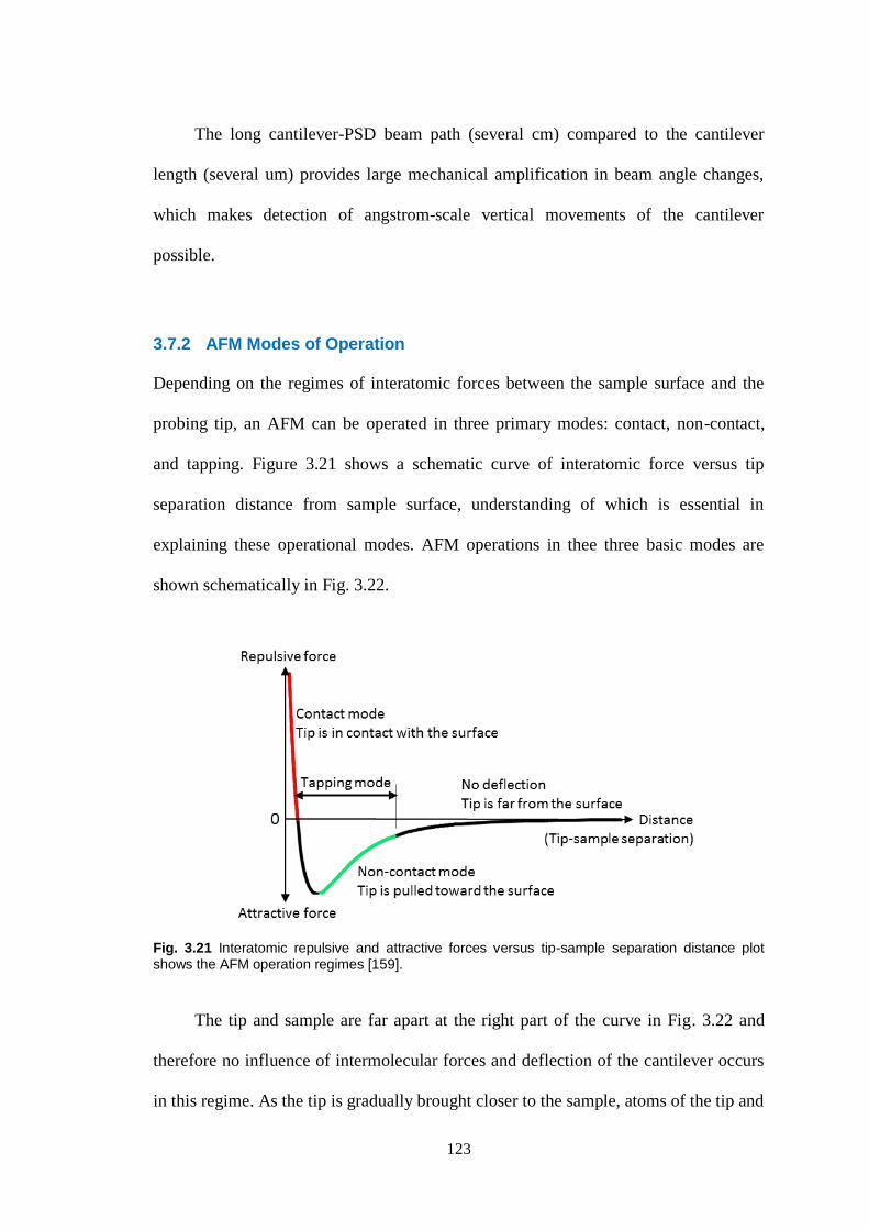
123
The long cantilever-PSD beam path (several cm) compared to the cantilever
length (several um) provides large mechanical amplification in beam angle changes,
which makes detection of angstrom-scale vertical movements of the cantilever
possible.
3.7.2 AFM Modes of Operation
Depending on the regimes of interatomic forces between the sample surface and the
probing tip, an AFM can be operated in three primary modes: contact, non-contact,
and tapping. Figure 3.21 shows a schematic curve of interatomic force versus tip
separation distance from sample surface, understanding of which is essential in
explaining these operational modes. AFM operations in thee three basic modes are
shown schematically in Fig. 3.22.
Fig. 3.21 Interatomic repulsive and attractive forces versus tip-sample separation distance plot shows the AFM operation regimes [159].
The tip and sample are far apart at the right part of the curve in Fig. 3.22 and
therefore no influence of intermolecular forces and deflection of the cantilever occurs
in this regime. As the tip is gradually brought closer to the sample, atoms of the tip and

124
the sample begin to weakly attract each other. This attraction force increases until the
atoms are so close to each other that corresponding electron clouds begin to repel each
other. This electrostatic repulsion progressively balances the attractive force as the
separation between the tip and sample continues to decrease. The total force goes
through zero at perfect balance between attractive and repulsive force and finally
becomes completely repulsive.
In contact mode AFM (Fig. 3.22(a)), the tip is held in continuous contact with
the sample surface usually maintaining a distance of only a few angstroms in between.
The tip, therefore, experiences repulsive force (Fig. 3.21) during the scan under the
influence of which the cantilever bends away from the sample rather than taking the
tip closer to the sample as the cantilever pushes the tip towards the sample in order to
make a hard contact. For adequate cantilever deflection, the stiffness of the cantilever
needs to be less than the effective spring constant that holds atoms of most solids
together, which is in the order of 1-10 nN/nm; and most of the contact mode
cantilevers, therefore, have a low spring constant less than 1 nN/nm.
Once the cantilever deflection is measured using the beam deflection method,
(Fig. 3.20) the AFM in contact mode can generate the topographic data in one of the
two ways – constant-height mode or constant-force mode. In constant-height mode,
the z feedback is turned off and the spatial variation of the cantilever deflection
generates the topographic data set. Whereas, z feedback is turned on in constant-force
mode and the image is based on the variation of movements in the z direction to
maintain a constant cantilever deflection.
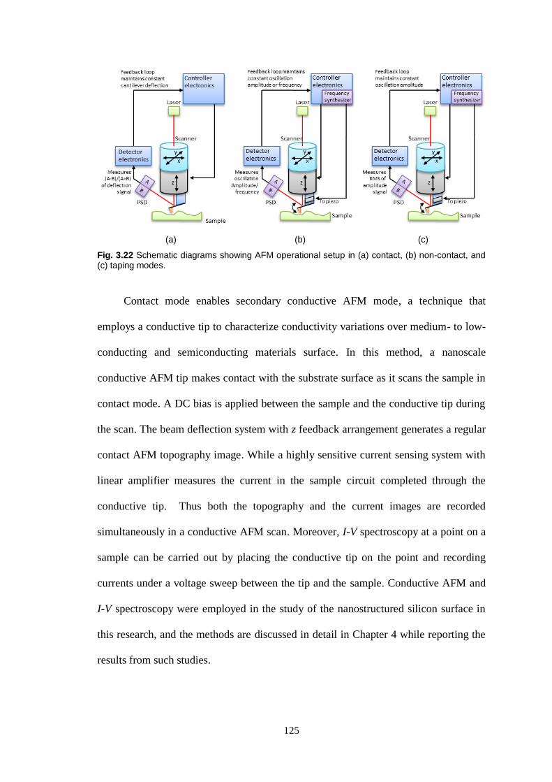
125
(a) (b) (c)
Fig. 3.22 Schematic diagrams showing AFM operational setup in (a) contact, (b) non-contact, and (c) taping modes.
Contact mode enables secondary conductive AFM mode, a technique that
employs a conductive tip to characterize conductivity variations over medium- to low-
conducting and semiconducting materials surface. In this method, a nanoscale
conductive AFM tip makes contact with the substrate surface as it scans the sample in
contact mode. A DC bias is applied between the sample and the conductive tip during
the scan. The beam deflection system with z feedback arrangement generates a regular
contact AFM topography image. While a highly sensitive current sensing system with
linear amplifier measures the current in the sample circuit completed through the
conductive tip. Thus both the topography and the current images are recorded
simultaneously in a conductive AFM scan. Moreover, I-V spectroscopy at a point on a
sample can be carried out by placing the conductive tip on the point and recording
currents under a voltage sweep between the tip and the sample. Conductive AFM and
I-V spectroscopy were employed in the study of the nanostructured silicon surface in
this research, and the methods are discussed in detail in Chapter 4 while reporting the
results from such studies.

126
The separation between the tip and the sample for non-contact AFM operation
(Fig. 2.22(b)) is in the range of tens to hundreds of angstroms, corresponding to a
weaker attractive inter-atomic force regime (Fig. 3.21). Here, a stiff cantilever
oscillates in the z-direction near its resonant frequency (typically 100 - 400 kHz) with
amplitude of a few tens to hundreds of angstroms under excitation from a voltage
controlled piezo-actuator. The system detects changes in the cantilever’s resonance
frequency or oscillation amplitude as the tip scans the sample surface. Constant
resonance frequency or oscillation amplitude is maintained through z feedback by
moving up or down in response to variations in z-direction and keeping the separation
and force between the tip and sample constant.
Tapping mode (Fig. 3.22(c)) is similar to non-contact mode operation in that a
stiff cantilever is oscillated in the attractive regime, but with part of the oscillation
extends into the repulsive regime (Fig. 3.21), so the tip can touch or tap the surface
occasionally. The feedback loop electronics in this case maintains constant oscillation
amplitude. The scheme increases the z resolution with respect to non-contact mode
without introducing the damage that may be caused by continuous contact. By
eliminating lateral forces it increases the x-y resolution of contact mode imaging. In
addition, since the vertical oscillation amplitude can reach about a few tens of
nanometres in tapping mode operation, higher than that in non-contact mode, it
overcomes the non-contact mode problem of tip sticking in thin liquid layer, a layer
that usually is found to cover a surface in ambient non-vacuum imaging environment.
3.7.3 Other Aspects of AFM
AFM imaging is not free from its glitches and can produce many types of image
artefacts. These artefacts are produced primarily as results of tip and surface condition,

127
tip convolution and shape, non-optimum scan and feedback parameter setup, and/or
the very nature of an AFM’s mechanical behaviour.
Worn tip or tip with attached debris results in features with the same shape
everywhere. Double or multiple images are formed with a tip with two or more end
points. Loss of image resolution or streaking can occur from loose debris on sample
surface. New tip and clean sample surface minimise these artefacts.
Most and worst image artefacts arise from tip convolution. Data points in a
AFM image represent a spatial convolution of the shape of the tip and the shape of the
feature scanned [160] with edge profile determined by the sharper of the two. Thus a
true edge profile of the feature can only be achieved if the tip has steeper slope edge or
lower aspect (width to height) ratio, than the feature. If the feature is sharper than the
tip instead, the image results as if the tip is scanned by the feature.
Feature broadening in lateral (x, y) dimensions and possible alterations in
vertical (z) direction especially in case of deep narrow trench due to tip convolution
and tip shape are shown schematically in Fig. 3.23. If images are dominated by tip-
convolution effects, change to another sharper tip is required. Alternatively, with prior
confirmation of the tip’s profile a de-convolution algorithm can be run on the image to
reverse the effect.
Fig. 3.23 Feature broadening and alterations can occur as results of tip convolution.
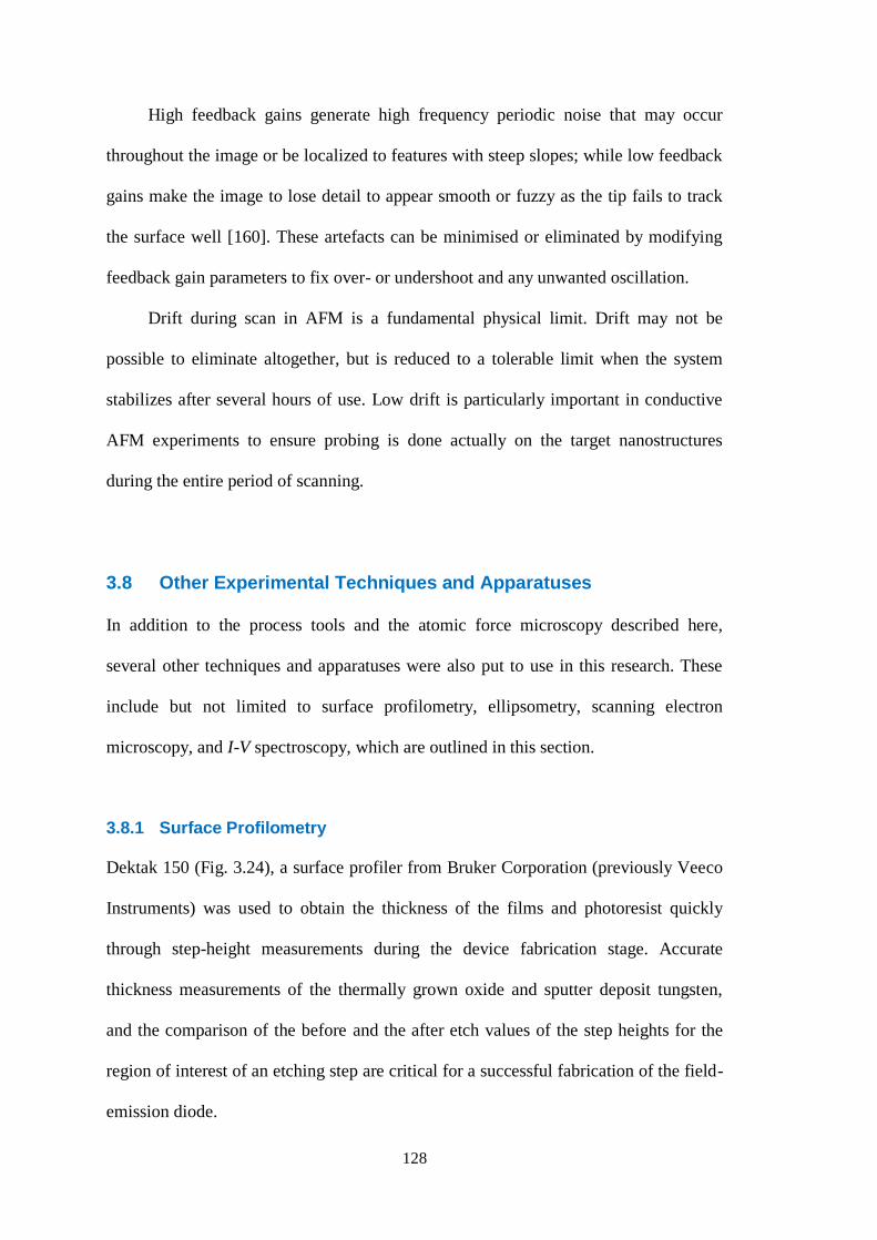
128
High feedback gains generate high frequency periodic noise that may occur
throughout the image or be localized to features with steep slopes; while low feedback
gains make the image to lose detail to appear smooth or fuzzy as the tip fails to track
the surface well [160]. These artefacts can be minimised or eliminated by modifying
feedback gain parameters to fix over- or undershoot and any unwanted oscillation.
Drift during scan in AFM is a fundamental physical limit. Drift may not be
possible to eliminate altogether, but is reduced to a tolerable limit when the system
stabilizes after several hours of use. Low drift is particularly important in conductive
AFM experiments to ensure probing is done actually on the target nanostructures
during the entire period of scanning.
3.8 Other Experimental Techniques and Apparatuses
In addition to the process tools and the atomic force microscopy described here,
several other techniques and apparatuses were also put to use in this research. These
include but not limited to surface profilometry, ellipsometry, scanning electron
microscopy, and I-V spectroscopy, which are outlined in this section.
3.8.1 Surface Profilometry
Dektak 150 (Fig. 3.24), a surface profiler from Bruker Corporation (previously Veeco
Instruments) was used to obtain the thickness of the films and photoresist quickly
through step-height measurements during the device fabrication stage. Accurate
thickness measurements of the thermally grown oxide and sputter deposit tungsten,
and the comparison of the before and the after etch values of the step heights for the
region of interest of an etching step are critical for a successful fabrication of the field-
emission diode.
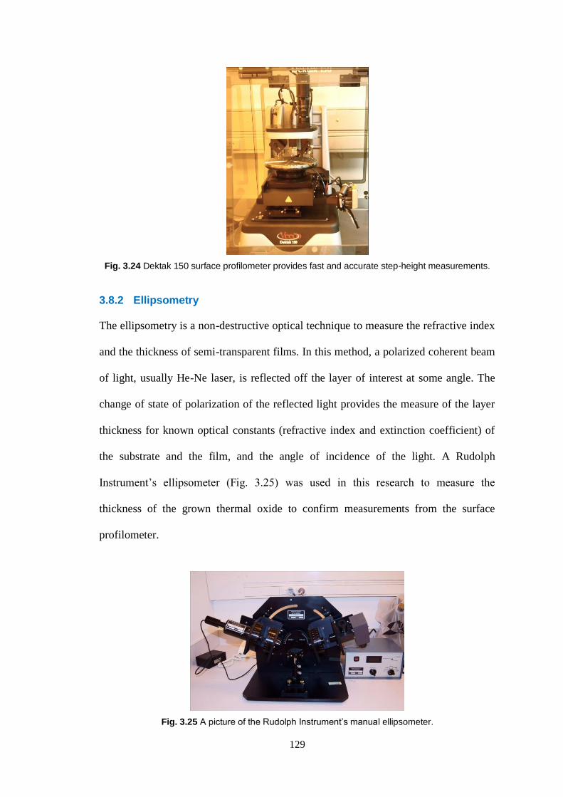
129
Fig. 3.24 Dektak 150 surface profilometer provides fast and accurate step-height measurements.
3.8.2 Ellipsometry
The ellipsometry is a non-destructive optical technique to measure the refractive index
and the thickness of semi-transparent films. In this method, a polarized coherent beam
of light, usually He-Ne laser, is reflected off the layer of interest at some angle. The
change of state of polarization of the reflected light provides the measure of the layer
thickness for known optical constants (refractive index and extinction coefficient) of
the substrate and the film, and the angle of incidence of the light. A Rudolph
Instrument’s ellipsometer (Fig. 3.25) was used in this research to measure the
thickness of the grown thermal oxide to confirm measurements from the surface
profilometer.
Fig. 3.25 A picture of the Rudolph Instrument’s manual ellipsometer.

130
3.8.3 Scanning Electron Microscopy
The scanning electron microscopy (SEM) is a standard surface analytical technique
where the electron microscope images a sample surface by scanning it with a highly-
focussed electron beam. The high-energy primary electrons from the beam enter the
surface and generate many low energy secondary electrons, the intensity of which
depends on the surface topography. An image is constructed by plotting secondary
electron intensity as a function of the position of the scanning beam. Since electron
beam can be focused to a spot below 10 nm, high resolution images of the surface
topography with excellent depth of field are produced by SEM. A LEO 1500 series
SEM integrated in the Raith 150 electron beam lithography system (Fig. 3.26) was
used in this research for imaging of the sample surfaces and cross sections.
Fig. 3.26 A picture of the Raith 150 electron beam lithography system, which hosts the LEO 1500 series scanning electron microscope.
3.8.4 I-V Characterization
Electrical current-voltage (I-V) measurements were carried out for the fabricated
device using a Hewlett Packard HP 4155A parameter analyser (Fig. 3.27). The detail
of the I-V characterization technique including experimental setup is included in
Chapter 6.

131
Fig. 3.27 A photograph of HP 4155A, a semiconductor parameter analyser used for I-V measurements of the field-emission diode.
3.9 Summary
Integrated field-emission diodes using nanostructured silicon surface as emitting
cathode were fabricated and characterized using the apparatuses and methods
discussed in this chapter. The fabrication comprises oxidation, photolithography, ion
implantation, etching, metallization, and electron-beam annealing and the
characterization surface topography, and surface and device electrical measurements.
The nanostructured silicon surface was investigated to relate its surface topography
with electrical properties in a conductive AFM study which is reported in detail in the
next chapter. The fabrication process of the complete integrated field-emission diode
is detailed in Chapter 5.

132

133
Chapter 4
CONDUCTIVE AFM STUDIES OF SELF-ASSEMBLED
SILICON NANOSTRUCTURES
The reporting of experiments and studies undertaken in this research and the results
therefrom along with the relevant analysis, as outlined in Section 1.5, are divided into
four major parts, namely, the conductive AFM studies of individual self-assembled
silicon nanostructures, the fabrication of the integrated field-emission diode using the
self-assembled silicon nanostructured cathode, the electrical characterization of the
fabricated diode, and the modelling and simulation of the field enhancement
phenomena encountered at the individual nanostructure and the device level. This
chapter begins the reporting with the conductive AFM studies performed in this
research, part of which was published in the Journal of Vacuum Science &
Technology B: Microelectronics and Nanometer Structures [161].
4.1 Introduction
Nanostructured silicon surface was used as the emitting cathode in the fabricated field-
emission device. The growth of these self-assembled quasi-one-dimensional
nanostructures on untreated n- and p-type silicon surfaces was confirmed in a simple
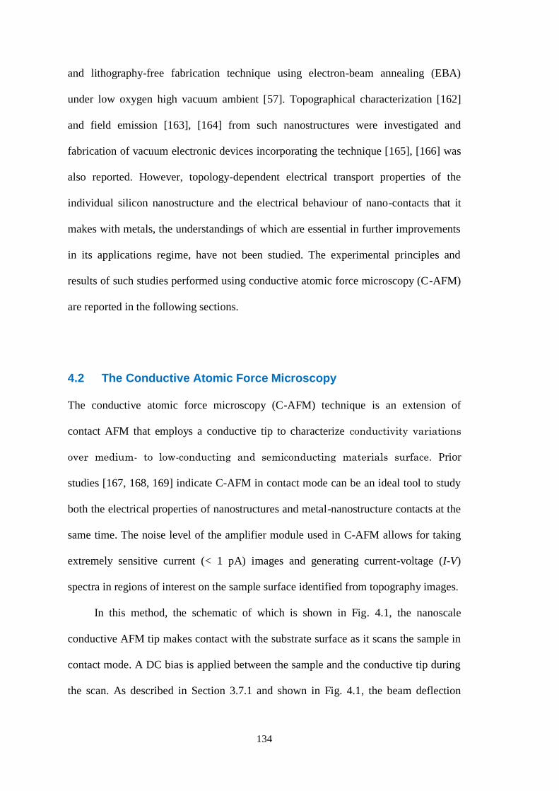
134
and lithography-free fabrication technique using electron-beam annealing (EBA)
under low oxygen high vacuum ambient [57]. Topographical characterization [162]
and field emission [163], [164] from such nanostructures were investigated and
fabrication of vacuum electronic devices incorporating the technique [165], [166] was
also reported. However, topology-dependent electrical transport properties of the
individual silicon nanostructure and the electrical behaviour of nano-contacts that it
makes with metals, the understandings of which are essential in further improvements
in its applications regime, have not been studied. The experimental principles and
results of such studies performed using conductive atomic force microscopy (C-AFM)
are reported in the following sections.
4.2 The Conductive Atomic Force Microscopy
The conductive atomic force microscopy (C-AFM) technique is an extension of
contact AFM that employs a conductive tip to characterize conductivity variations
over medium- to low-conducting and semiconducting materials surface. Prior
studies [167, 168, 169] indicate C-AFM in contact mode can be an ideal tool to study
both the electrical properties of nanostructures and metal-nanostructure contacts at the
same time. The noise level of the amplifier module used in C-AFM allows for taking
extremely sensitive current (< 1 pA) images and generating current-voltage (I-V)
spectra in regions of interest on the sample surface identified from topography images.
In this method, the schematic of which is shown in Fig. 4.1, the nanoscale
conductive AFM tip makes contact with the substrate surface as it scans the sample in
contact mode. A DC bias is applied between the sample and the conductive tip during
the scan. As described in Section 3.7.1 and shown in Fig. 4.1, the beam deflection
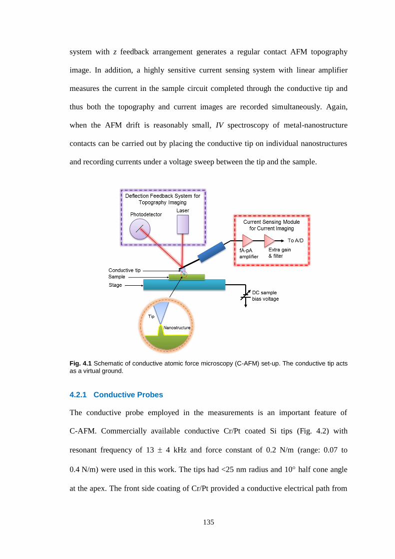
135
system with z feedback arrangement generates a regular contact AFM topography
image. In addition, a highly sensitive current sensing system with linear amplifier
measures the current in the sample circuit completed through the conductive tip and
thus both the topography and current images are recorded simultaneously. Again,
when the AFM drift is reasonably small, IV spectroscopy of metal-nanostructure
contacts can be carried out by placing the conductive tip on individual nanostructures
and recording currents under a voltage sweep between the tip and the sample.
Fig. 4.1 Schematic of conductive atomic force microscopy (C-AFM) set-up. The conductive tip acts as a virtual ground.
4.2.1 Conductive Probes
The conductive probe employed in the measurements is an important feature of
C-AFM. Commercially available conductive Cr/Pt coated Si tips (Fig. 4.2) with
resonant frequency of 13 4 kHz and force constant of 0.2 N/m (range: 0.07 to
0.4 N/m) were used in this work. The tips had <25 nm radius and 10 half cone angle
at the apex. The front side coating of Cr/Pt provided a conductive electrical path from
136
the apex of the tip to the cantilever holder chip through the cantilever. The pre-coat tip
and the cantilever were both made up of micro-machined monolithic Si. The coated
noble metal film also caused the tip to be more durable against tip deterioration from
contact mode imaging. Tip wear can be problematic especially for C-AFM as in
addition to generating topography image artefacts from the worn tip, a loss of
conductivity from exposure of underlying silicon tip may occur rendering the current
sensing ineffectual. The backside coating of Cr/Pt compensated the stress created by
the front side coating and served to provide reasonable reflective laser signal for the
deflection feedback system.
Fig. 4.2 Images of conductive AFM probe tip. Schematics are taken from the commercial brochure [170].
4.2.2 The TUNA Application Module
The commercially available TUNA (tunnelling AFM) application module was used in
the C-AFM work and is shown in Fig. 4.3. The TUNA application module comes with

137
a specially designed AFM scanner head that allows mounting on it a sensor module,
which contains the current amplification circuit required for ultra-low current
measurements. A special tip holder provides electrical connection from the tip holder
die to the sensor while maintaining standard features for topographic imaging. The
TUNA sensor module is an extension and connected to the standard electronics box of
the AFM system.
Fig. 4.3 Image of TUNA application module AFM scanner, where TUNA sensor is mounted on the side. Conductive tip is loaded on TUNA tipholder, which is mounted under the bottom stage of the scanner and connected to TUNA sensor. Tuna sensor is also connected to the AFM electronics box.
The gain of the TUNA sensor is as high as 1012
, which corresponds to a current
sensitivity of 1 pA/V. It can sense currents in the range of 80 fA to 120 pA. The
module has a bias limit of 12V, and thus a maximum of 12V can be applied between
the sample and tip. As for I-V spectroscopy, the module allows for 16 to 64,000
samples per sweep while limiting a maximum of 1,024 sweeps to be averaged for one
reading. The TUNA module can also be used in advanced lift-mode interleave scan
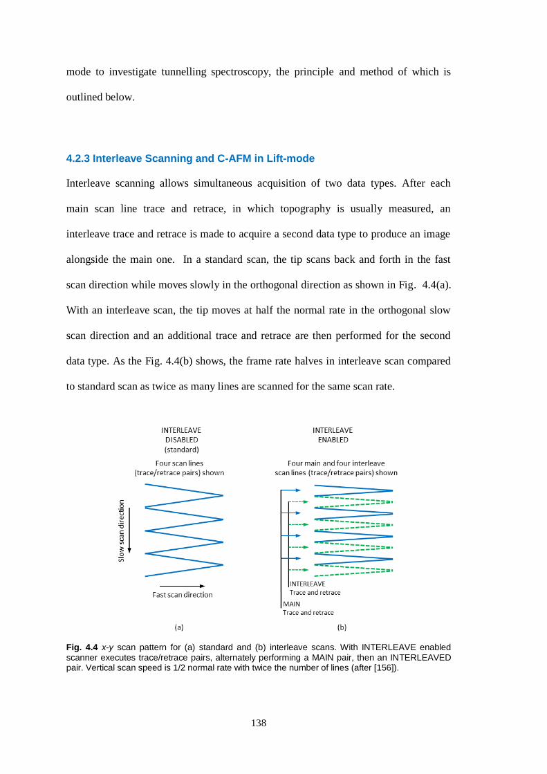
138
mode to investigate tunnelling spectroscopy, the principle and method of which is
outlined below.
4.2.3 Interleave Scanning and C-AFM in Lift-mode
Interleave scanning allows simultaneous acquisition of two data types. After each
main scan line trace and retrace, in which topography is usually measured, an
interleave trace and retrace is made to acquire a second data type to produce an image
alongside the main one. In a standard scan, the tip scans back and forth in the fast
scan direction while moves slowly in the orthogonal direction as shown in Fig. 4.4(a).
With an interleave scan, the tip moves at half the normal rate in the orthogonal slow
scan direction and an additional trace and retrace are then performed for the second
data type. As the Fig. 4.4(b) shows, the frame rate halves in interleave scan compared
to standard scan as twice as many lines are scanned for the same scan rate.
Fig. 4.4 x-y scan pattern for (a) standard and (b) interleave scans. With INTERLEAVE enabled scanner executes trace/retrace pairs, alternately performing a MAIN pair, then an INTERLEAVED pair. Vertical scan speed is 1/2 normal rate with twice the number of lines (after [156]).

139
Lift mode (Fig. 4.5) can be enacted in an interleave scan. In this case, during the
interleave trace and retrace, the tip is lifted to a user-selected height above the surface
and the feedback control is turned off to perform far field measurements such as
magnetic force microscopy (MFM) and electric force microscopy (EFM). The tip first
is pulled away from the surface to a large lift start height in order to eliminate sticking
and then moved to the lift scan height. The tip maintains the height from the surface
during the interleave pass by adding the lift scan height point-by-point to the
topography data recorded during the main pass.
Fig. 4.5 Interleave lift mode scanning. Lift mode scan starts with lifting the tip to pre-set lift start height and then quickly come back to the pre-set lift scan height to complete the interleave trace.
The feedback laser is not necessarily required during the lift line scan as the
surface topography has already been recorded during the main scan. The feedback
control, therefore, can be turned off during the interleave pass. This is particularly
helpful in experiments where light from laser source can influence experiments such
as in case of semiconductors. With the conductive tip and the TUNA sensor, field
emission from the surface nanostructures can be measured at selective distances above
such structures using the interleave scan.
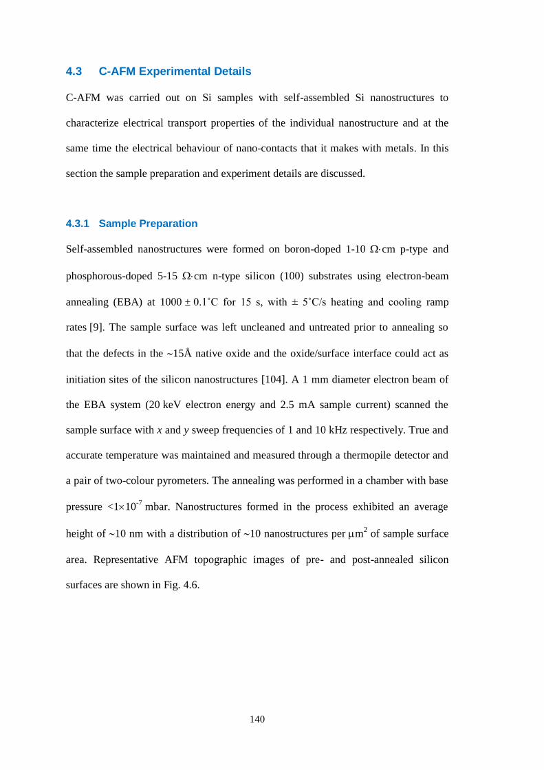
140
4.3 C-AFM Experimental Details
C-AFM was carried out on Si samples with self-assembled Si nanostructures to
characterize electrical transport properties of the individual nanostructure and at the
same time the electrical behaviour of nano-contacts that it makes with metals. In this
section the sample preparation and experiment details are discussed.
4.3.1 Sample Preparation
Self-assembled nanostructures were formed on boron-doped 1-10 cm p-type and
phosphorous-doped 5-15 cm n-type silicon (100) substrates using electron-beam
annealing (EBA) at 1000 ± 0.1˚C for 15 s, with ± 5˚C/s heating and cooling ramp
rates [9]. The sample surface was left uncleaned and untreated prior to annealing so
that the defects in the 15Å native oxide and the oxide/surface interface could act as
initiation sites of the silicon nanostructures [104]. A 1 mm diameter electron beam of
the EBA system (20 keV electron energy and 2.5 mA sample current) scanned the
sample surface with x and y sweep frequencies of 1 and 10 kHz respectively. True and
accurate temperature was maintained and measured through a thermopile detector and
a pair of two-colour pyrometers. The annealing was performed in a chamber with base
pressure <110-7
mbar. Nanostructures formed in the process exhibited an average
height of 10 nm with a distribution of 10 nanostructures per m2 of sample surface
area. Representative AFM topographic images of pre- and post-annealed silicon
surfaces are shown in Fig. 4.6.
141
Fig. 4.6 AFM images of silicon surfaces before and after electron beam annealing (EBA), a simple CMOS process-compatible method to form self-assembled nanostructures.
4.3.2 Measurements
The C-AFM measurements of the nanostructured samples were carried out under
standard atmospheric conditions at room temperature using a Bruker Corporation’s
Dimension 3100 AFM system (Section 3.7) with conductive Cr/Pt coated Si tips
(Section 4.2.1) loaded in TUNA tip holder (Section 4.2.2). Samples were placed on the
chuck and vacuum was used to hold the samples in place and in close contact with the
stage and the sample surface was scanned for normal topographic and current images
at different low voltage biases – both negative and positive. Bias voltages > 1 V or < -
1 V resulted in tip-induced oxidation of the sample surface and was manifested by low
or no current in subsequent scans on such areas and showing bumps in the topographic
images, hence such ‘extreme’ voltages were avoided.

142
Once nanostructures had been identified during any such scan, I-V spectroscopy
measurements were performed on individual nanostructures with applied bias voltages
ramped from -0.5 V to +0.5 V DC. Stable I-V readings were possible after allowing
sample positional drift to reduce to as low as several nanometres per minute on the
AFM system. I-V spectroscopy (bias voltage sweep -1 to +1 V DC) was also carried
out on flat surfaces of the samples for the collection of comparison data. The results of
these measurements are discussed in Section 4.4 in detail.
4.3.3 Precautions
C-AFM measurements are extremely sensitive to noise. Since the sensor can sense
ultra-low currents, the system can also amplify any unwanted external disturbances.
Care was taken to minimize effects of disruptive electronic equipment which includes
but not limited to oscilloscopes, fluorescent lights, and other electronic equipment
operated in close proximity. The stage and its surrounding areas are electrostatically
sensitive and an enclosure with hood with acoustic and electrical screening was always
used during C-AFM measurements.
4.4 C-AFM Results and Discussion
The results from the conductive atomic force microscopy are reported under two
sections: conductive scan and I-V spectroscopy. I-V spectroscopy results were
analysed theoretically.
4.4.1 Standard Conductive Scan Results
A series of topographic and current images captured during the initial C-AFM scans of
11 m2 p-type sample areas for bias voltages from -1 V to +1 V is shown in Fig. 4.7.

143
Fig. 4.7 C-AFM scans of the 1x1 m2 sample (p-type Si) area at different bias voltages. For each
set of images, the left image shows topography and the right current.

144
The topographic images were set in discrete height scale to highlight distinctly the
nanostructures from their surrounding flat field area of a sample surface. An
association between the topography and current images became evident, In the current
images, the currents when the conductive tip was on nanostructured areas (observable
from the corresponding topography image) were noticed to pass from a negative
extreme (dark brown) towards zero (light brown), to change sign after crossing zero
(light yellow), and then to a positive extreme (dark yellow to pinkish) as bias voltage
of the scans changed from -1 V to +1 V.
The current behaviour noticed above was probed further for bias scans of -1 and
+1 V DC respectively. The respective scanned topography and current images are
reproduced in Fig. 4.8 and in Fig. 4.9 along with line traces of the topography and
current signals over the same scan-line position. The images again reveal an
unambiguous correlation between the topography (Fig. 4.8(a),(c) and Fig. 4.9(a),(c))
and current flow (Fig. 4.8(b),(d) and Fig. 4.9(b),(d)) on the surface indicating
nanostructured areas to be more conductive than their flat vicinity.
The current traces (Fig. 4.8(d) and Fig. 4.9(d)) showed that the current on the
nanostructures is typically orders of magnitude higher than that on the surrounding flat
silicon at low voltages. The current polarity is also observed to change as the tip bias
polarity is changed (Fig. 4.8(d) versus Fig. 4.9(d)).
It is to be noted that the line traces of the topography and current signals in
Fig. 4.8 and Fig. 4.9 are taken across an arbitrary horizontal line. They represent
height and current data for the particular points on the line only and as such may not
represent the maximum current in a particular nanostructure that may occur at a
different point on the nanostructure.

145
Fig. 4.8 Representative (a) topographic and (b) current C-AFM images of a p-type sample
biased at -1.0 V DC (11 m2 scans). (c) Line trace of the topography and (d) line trace of the current signals at the marked positions in (a) and (b) respectively.
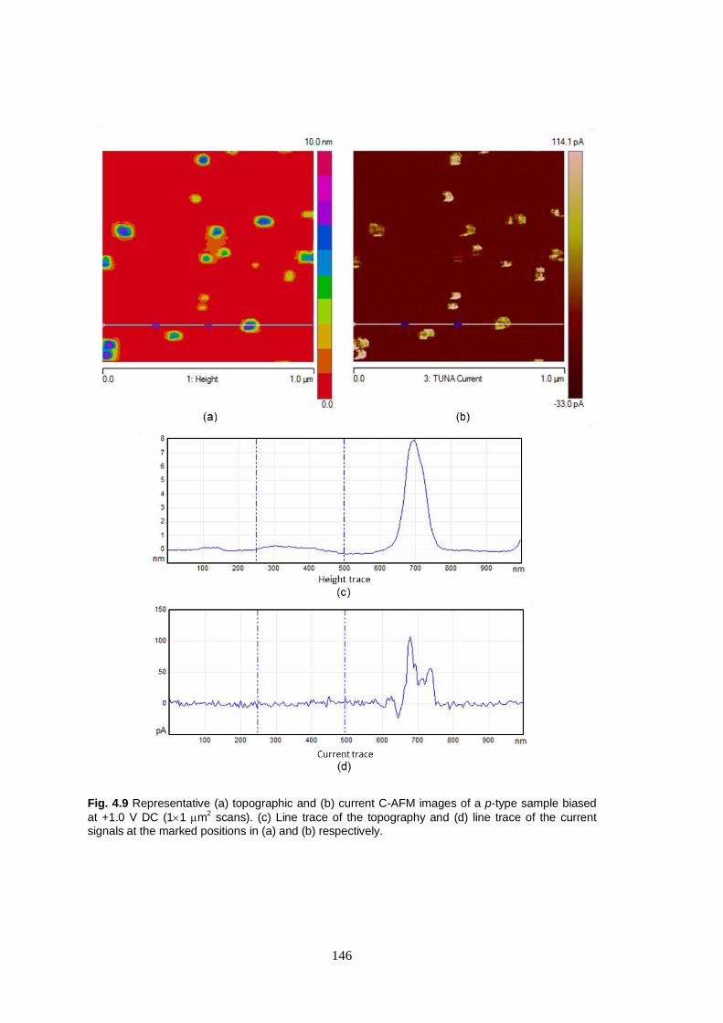
146
Fig. 4.9 Representative (a) topographic and (b) current C-AFM images of a p-type sample biased
at +1.0 V DC (11 m2 scans). (c) Line trace of the topography and (d) line trace of the current
signals at the marked positions in (a) and (b) respectively.

147
4.4.2 I-V Spectroscopy Results
Representative I-V spectroscopy results on a nanostructure apex and surrounding flat
silicon field area for p-type samples are shown in Fig. 4.10. Current at the tip-field
contact for p-type silicon (Fig. 4.10(a)) is very low (pA level) and is in the noise
regime of the TUNA sensor. However, an offset hysteresis in trace and retrace currents
and ringing of currents at the beginning of these scans were observed. These effects
can be explained by the capacitive charging and discharging and the LC resonance in
the measurement circuit. At tip and p-type silicon nanostructure contacts, exponential
increase in current was observed (Fig. 4.10(b)) in the positive bias region. The current
in the negative bias region was flatter at lower voltage.
Fig. 4.10 Current-voltage (I-V) spectroscopy curves. Measurements were taken at a point on (a) flat, and (b) a nanostructure of a p-type silicon surface.
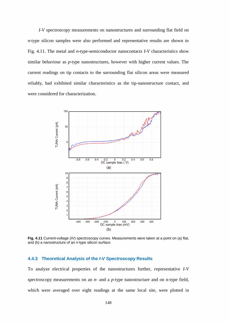
148
I-V spectroscopy measurements on nanostructures and surrounding flat field on
n-type silicon samples were also performed and representative results are shown in
Fig. 4.11. The metal and n-type-semiconductor nanocontacts I-V characteristics show
similar behaviour as p-type nanostructures, however with higher current values. The
current readings on tip contacts to the surrounding flat silicon areas were measured
reliably, had exhibited similar characteristics as the tip-nanostructure contact, and
were considered for characterization.
Fig. 4.11 Current-voltage (IV) spectroscopy curves. Measurements were taken at a point on (a) flat, and (b) a nanostructure of an n-type silicon surface.
4.4.3 Theoretical Analysis of the I-V Spectroscopy Results
To analyze electrical properties of the nanostructures further, representative I-V
spectroscopy measurements on an n- and a p-type nanostructure and on n-type field,
which were averaged over eight readings at the same local site, were plotted in
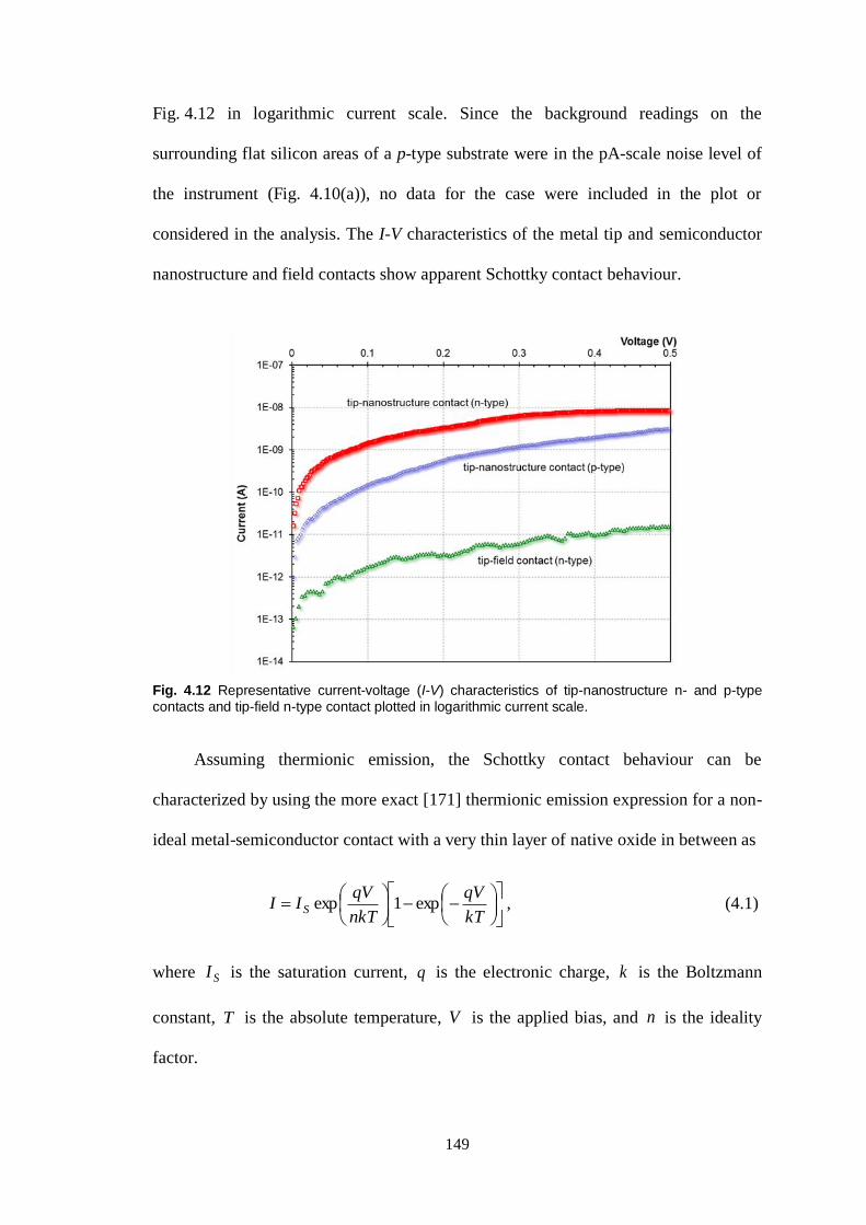
149
Fig. 4.12 in logarithmic current scale. Since the background readings on the
surrounding flat silicon areas of a p-type substrate were in the pA-scale noise level of
the instrument (Fig. 4.10(a)), no data for the case were included in the plot or
considered in the analysis. The I-V characteristics of the metal tip and semiconductor
nanostructure and field contacts show apparent Schottky contact behaviour.
Fig. 4.12 Representative current-voltage (I-V) characteristics of tip-nanostructure n- and p-type contacts and tip-field n-type contact plotted in logarithmic current scale.
Assuming thermionic emission, the Schottky contact behaviour can be
characterized by using the more exact [171] thermionic emission expression for a non-
ideal metal-semiconductor contact with a very thin layer of native oxide in between as
kT
qV
nkT
qVII S exp1exp , (4.1)
where SI is the saturation current, q is the electronic charge, k is the Boltzmann
constant, T is the absolute temperature, V is the applied bias, and n is the ideality
factor.
150
The saturation current SI is specified by
kT
qATAI B
S exp2** , (4.2)
where **A is the effective Richardson constant, A is the area of the diode, in this
quasi-1D nanostructure case the contact area, and B is the Schottky barrier height of
the contact.
Effective Richardson constants **A of 112 A/cm2K
2 for electrons in n-type and
32 A/cm2K
2 for holes in p-type silicon that take into account the effects from
anisotropy of carrier effective masses, scattering by optical phonons, and quantum
mechanical reflection and tunneling at the metal-semiconductor junction [172] were
used in the calculations. The effective contact area for nanostructures was
approximated by using the nanostructure apex radius of 1 nm, the smaller of the
radiuses of the tip and nanostructure apexes. For the flat field contacts, the effective
contact area is approximated using the radius of the tip apex, i.e., 25 nm.
Ideality factor n and barrier height B are determined from the above
equations. In the forward bias operation for voltages, qkTV /3 , Eq. (4.1) is reduced
for forward current IF to
nkT
qVIII
SFexp . (4.3)
Eq. (4.3) can then be rewritten as
SF IVnkT
qI lnln
, (4.4)
from which n can be extracted from the slope of the linear region of the semi-
logarithmic plot of FIln vs. V . Figure 4.11 shows the linear region,

151
qkTVqkT /4/3 , of the I-V curve considered for the linear fit for the extraction of
relevant parameters.
Fig. 4.13 ln IF vs V curve in the linear region 3kT/q < V < 4kT/q and its linear fit with the corresponding equation.
The saturation current SI is extracted from the y intercept of the linear fit to
calculate the effective barrier height which is now given by
2**ln
ATA
I
q
kT SB . (4.5)
Extracted values of different parameters are listed in Table 4.1. B values found
(0.17-0.55 eV) are lower than that reported [173] (0.81 eV) for macroscopic Pt
diodes on silicon. Schottky barrier height (SBH) of 0.17 – 0.21 eV indicates the
lowering to be more prominent for metal-nanostructure nanocontacts than for metal-
flat nanocontacts which exhibited B range of 0.49 – 0.55 eV. Surface states in
different facets of the nanostructures and the resulting image force contribute to the
SBH lowering [174]. The current non-uniformities at different facets of the
nanostructures as seen in the current cross-sections through the nanostructures
(Fig. 4.8 and Fig. 4.9) support the findings.

152
Table 4.1 Extracted electrical parameters for metal-silicon nanocontacts.
Type of
nanocontact
Richardson
constant
A** in A/cm2K
2
Effective
contact area
A in cm2
Ideality
factor
n
Saturation
current
IS in A
Effective barrier
height
B in eV
metal-
nanostructure
(p-type Si)
32 3.1410-14
2.03 – 2.84 10-11
0.19 – 0.21
metal-flat
(p-type Si) 32 1.9610
-11 - - -
metal-
nanostructure
(n-type Si)
112 3.1410-14
2.41 – 2.97 10-10
0.17-0.19
metal-flat
(n-type Si) 112 1.9610
-11 1.51 – 1.94 10
-12 0.49-0.55
All the measurements were performed in air environment under standard room temperature and pressure, i.e., T = 298 K.
Extracted high n (2.03-2.97) for metal-nanostructure nanocontacts signifies non-
ideal Schottky behaviour. This response specifies existence of current transport
mechanisms other than thermionic emission [168]. Under forward bias, minority
carrier injection from opposite-polarity semiconductor region adjacent to the thin-
oxide/metal layer into the bulk [175] could be a possible current transport mechanism.
Since minority carrier concentration in point contacts decreases at a distance r away
from the contact as 1/r spherically [176], diffusion rate may increase significantly for
nanocontacts. Also, high curvature of the nanostructure apex leads to field
enhancement and hence field emission from the nanostructures under forward bias,
could be another mechanism. Again, the grown oxide is thinner on convex
corners [177], i.e., at the nanostructure apex, than it is on the flat regions. Thinner
oxide layer could contribute to more tunnelling current between nanostructure and
metal tip, and therefore, higher n. In line with this particular observation, metal tip
contacts on n-type flat silicon surface, which has a relatively thicker oxide, showed
better ideality factor (1.51 – 1.94), though still to a great extent non-ideal. Again, field

153
enhancement in the metal-flat nanocontact setting may be limited by local atomic scale
roughness. Field enhancements were modelled and results of the simulations are
discussed in Chapter 7.
In the following section field emission from the nanostructured samples is
explored through measurements performed using conductive AFM in interleave lift
mode scan.
4.4.4 Interleave Lift-mode Conductive AFM Results
In an interleave scan, a conductive AFM tip can be lifted to a predetermined height
above a surface in lift-mode (Section 4.2.3), and current can be sensed by the TUNA
sensor at an adequate height and biasing voltage. All these opportunities presented by
the interleave scanning in lift-mode C-AFM were utilized to explore possibilities of
Fowler-Nordheim tunnelling or field emission from the nanostructured surface under
investigation.
The interleave lift-mode C-AFM was carried out with lift start height of 1 m
and at bias voltage of 0.5 V. Data were recorded for scans for various scan heights.
Each of the arrangements had been such that the nanostructures were the emitting sites
of the silicon cathode, and the conductive AFP tip the collecting anode, while the scan
height and the bias were the separation, d, and the applied voltage, V, between the two
electrodes respectively.
The images from one such microscopy with a p-type sample are collected in Fig.
4.14, which shows decaying of current as the separation d is increased. The falling-off
of current with increasing d follows the expected reduction of applied field (= V/d)
between the electrodes and thus also a corresponding reduction of the local field on the
nanostructure apex.
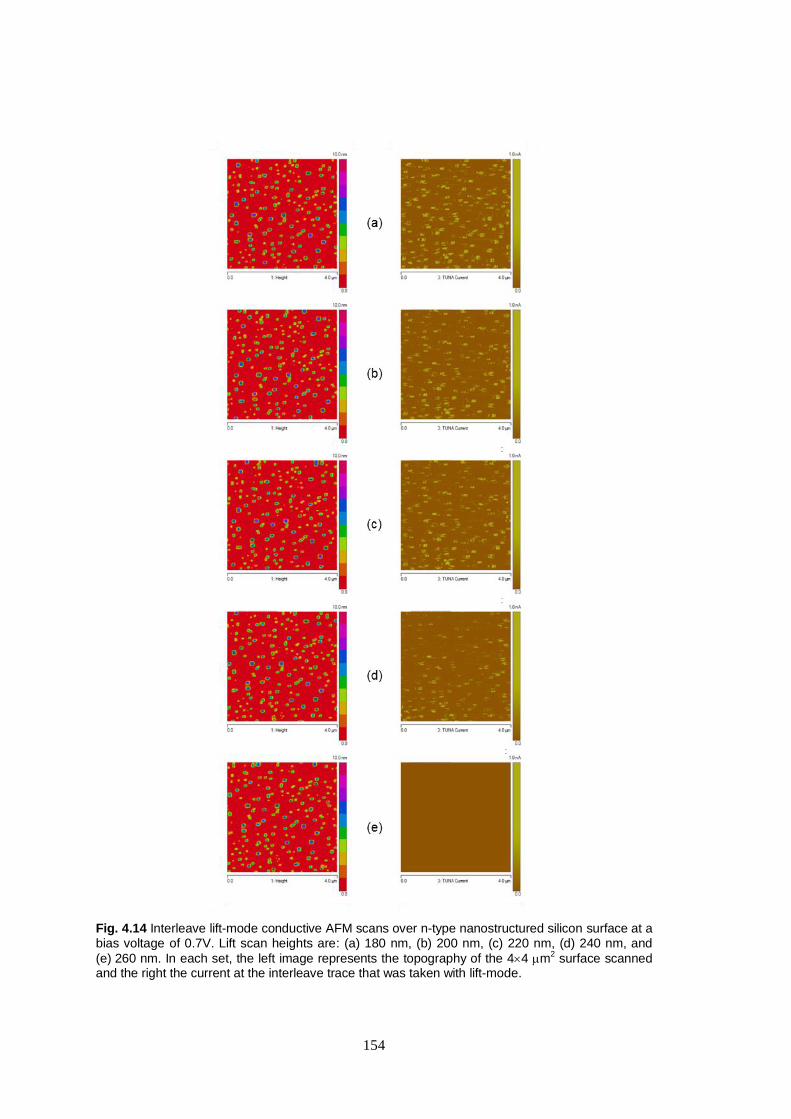
154
Fig. 4.14 Interleave lift-mode conductive AFM scans over n-type nanostructured silicon surface at a bias voltage of 0.7V. Lift scan heights are: (a) 180 nm, (b) 200 nm, (c) 220 nm, (d) 240 nm, and
(e) 260 nm. In each set, the left image represents the topography of the 44 m2 surface scanned
and the right the current at the interleave trace that was taken with lift-mode.

155
Respective topography images in Figs. 4.14(a-c) make it obvious that significant
field emission current was recorded from areas that showed sharper and taller
nanostructures for up to a separation d of 220 nm. In Fig. 4.14(d), d = 240 nm and
some of the relatively shorter and blunted nanostructures, which earlier had been
emitting had stopped doing so, while the emission from the others had become weaker.
And finally in Fig. 4.14(e), the recorded current died off (~ pA) or went into the noise
margin at d = 260 nm. These qualitative findings can lead to a preliminary quantitative
measure on the size of a turn-on applied field that may be required to initiate and
maintain field emission from the self-assembled silicon nanostructures under
investigation. The value of the said turn-on applied field for the majority of the
nanostructures arrived at from the above interpretive analysis then is given by
0.5 V/220 nm or 2.27106 V/m. If field emission requirement of a local field of
1109 V/m is considered, these nanostructures had exhibited field enhancement factors
in access of 440.
However, with this set up, spectroscopy was not made possible at a particular
point above the surface during the lift mode interleave trace, which prevented further
electrical analysis. Additional characterization, including local vacuum field emission
and vacuum I-V measurements, would be required to fully investigate the electrical
transport mechanisms in these self-assembled silicon nanostructures further. Our
relatively simple C-AFM system cannot perform such measurements at present.
4.5 Summary
The electrical transport characteristics of self-assembled silicon nanostructures were
investigated using C-AFM. Results showed an unambiguous correlation between the

156
topography and current flow on the nanostructured surface. Measured I-V
characteristics of individual tip-nanostructure contacts showed Schottky contact
behaviour. Thermionic emission through the thin native oxide layer was assumed and
the ideality factor and the Schottky barrier height were extracted. Extracted ideality
factor, 2.03-2.97 for metal-nanostructure and 1.51-1.94 for metal-flat silicon
nanocontacts, were high and non-ideal. Whereas, the extracted barrier height, 0.17-
0.21 for nanostructures and 0.49-0.55 for flat silicon, were lower than the macroscopic
value. Possibilities of surface states, image-force lowering of potential barrier, field
emission, and minority carrier injection were considered as reasons for low Schottky
barrier heights and high ideality factors. Likelihood of Fowler-Nordheim tunnelling or
field emission was explored in preliminary interleave lift mode AFM scans. Through
successful conductive AFM imaging, therefore, a primary understanding of the
different electrical transport mechanisms for nanostructures and the metal-
nanostructure behaviour has been made possible.

157
Chapter 5
FABRICATION OF INTEGRATED
FIELD EMISSION DIODES
An integrated field emission diode has the potential to bring advantages from both the
worlds – vacuum and solid-state electronics – together in one standing. Solid-state
electronics promise advanced fabrication technology, high packing density, and
therefore a greater economy of scale. On the other hand, vacuum electronics offer
higher speed with faster electron transport, temperature insensitivity, and radiation
hardness, and therefore a stronger operational command. With these basic
understandings in the background, ‘microelectronikers’ have developed and made use
of several techniques using various materials to fabricate field emission devices as
elaborated in Chapter 1 in general and in Section 2.6 in particular.
Self-assembled silicon nanostructures grown with electron-beam annealing
(EBA), a simple one-step lithography-free process, have become the potential
candidate for use as emitters for field emission devices, as they exhibited field
emission at low voltages. Johnson et al. reported field emission from these
nanostructured arrays at 100 m cathode-anode separation [163] and conductive AFM
158
investigations in this research have confirmed the same at such separation in the
nanometre scale. The conductive AFM results are reported in Chapter 4 of this thesis.
As the next step to find applications of these nanostructures, field emission devices
have been fabricated. Thongpang examined field emission diode structures fabricated
with EBA grown nanostructures on Separation by Implanted Oxygen (SIMOX)
Silicon on Insulator (SOI) wafers [165]. Lansley et al. reported fabrication of a triode
structure with an added third (gate) electrode that can control the device conduction
characteristics through biasing [166]. However, the devices were discrete and not
integrated in the Complementary Metal-Oxide-Semiconductor (CMOS) process flow
as such. This research completed the fabrication of the CMOS-compatible integrated
field emission diode with controlled growth of Si nanostructures for its cathode and
the present chapter describes the fabrication process in detail. The developed
fabrication process was reported orally in the 2010 Conference on Optoelectronic and
Microelectronic Materials and Devices (COMMAD) held in Canberra, Australia [178].
5.1 Introduction
The process flow for the fabrication of the integrated field emission diode incorporates
three photolithographic definition or pattern transfer steps, namely: contact to
substrate, metal anode and cathode plate terminals, and opening for cathode surface or
nanostructured area. Figure 3.1 is redrawn as Fig. 5.1 highlighting these steps.
Fabrication of masks required for pattern transfer in these steps is described first.
Details of the process steps that were followed and integrated in the fabrication of the
device are discussed next. Comments and observations on related process issues are
discussed at the end.

159
Fig. 5.1 Major fabrication process steps for field-emission diode based on silicon nanostructures. Three photolithographic pattern transfer steps are highlighted.
5.2 Mask Fabrication for Optical Lithography
A mask for optical lithography, i.e., a photomask, is usually a glass plate that contains
the pattern that is transferred to the sample in one exposure. The pattern on the mask is
normally generated by direct laser or e-beam writing from designed mask layout data
using a mask writer. The fabrication of photomasks for the three photolithographic
steps is detailed in the following sections.

160
5.2.1 Mask Layout
The design for the field-emission devices was laid out using L-Edit, a commercially
available Layout Editor from Tanner Research Inc. The design comprised data for
contact, metal, and nanostructure ‘layer’ area of the field-emission diodes and is
shown in Fig. 5.2.
(a) (b)
(c) (d)
Fig. 5.2 Images of drawn layers in L-Edit: (a) cathode contact, (b) metal, (c) cathode opening. (d) All these layers are stacked (bottom-to-top) to form the device structure.
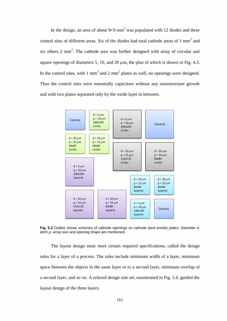
161
In the design, an area of about 99 mm2 was populated with 12 diodes and three
control sites of different areas. Six of the diodes had total cathode areas of 1 mm2 and
six others 2 mm2. The cathode area was further designed with array of circular and
square openings of diameters 5, 10, and 20 m, the plan of which is shown in Fig. 4.3.
In the control sites, with 1 mm2 and 2 mm
2 plates as well, no openings were designed.
Thus the control sites were essentially capacitors without any nanostructure growth
and with two plates separated only by the oxide layer in between.
Fig. 5.3 Outline shows schemes of cathode openings on cathode (and anode) plates. Diameter d, pitch p, array size and opening shape are mentioned.
The layout design must meet certain required specifications, called the design
rules for a layer of a process. The rules include minimum width of a layer, minimum
space between the objects in the same layer or to a second layer, minimum overlap of
a second layer, and so on. A relaxed design rule set, enumerated in Fig. 5.4, guided the
layout design of the three layers.
Control Control
Control
d = 5 m p = 10 m 100x100 circles
d = 5 m p = 10 m 200x200 circles
d = 10 m p = 15 m 66x66 circles
d = 20 m p = 25 m 40x40 circles
d = 10 m p = 15 m 132x132 circles
d = 10 m p = 15 m 66x66 squares
d = 20 m p = 25 m 80x80 circles
d = 20 m p = 25 m 40x40 squares
d = 5 m p = 10 m 100x100 squares
d = 5 m p = 10 m 200x200 squares
d = 10 m p = 15 m 132x132 squares
d = 20 m p = 25 m 80x80 squares

162
Design rules
C1 Minimum contact width 10 m
C2 Minimum space between contacts 10 m
M1 Miimum metal width 20 m
M2 Minimum space between metals 20 m
M3 Minimum metal overlap of contact 5 m M4 Minimum metal overlap of
nanostructure area 5 m
N1 Minimum width of nanostructure area 5 m N2 Minimum space between
nanostructure areas 5 m
Fig. 5.4 A relaxed design rule set for the integrated field emission diode.
Once the design was completed maintaining the design rules, the highest-level
cell was flattened and the individual layers were extracted in the DXF format, which
allowed transfer of curved object as was. These files were the inputs for the µPG 101
mask-writer (Fig. 3.7).
5.2.2 Transfer of Mask Layout to a Photomask
The mask-writer writes the designed patterns from the extracted input layer files
directly on a blank glass photomask plate. Nanofilm’s 440.60 print grade sensitized
blank glass photomask plates were used to fabricate the photolithography masks set.
These plates are soda lime glasses with about 100 nm coating of low reflective chrome
(Cr) on one side. The chrome was pre-coated with 530 nm of AZ1518, a positive
photoresist. The laser of the mask writer during the pattern transfer process exposed
this photoresist. Exposures were done at 25% of 8 mW.
There are two exposure modes – the ‘non-inverted’ mode to indicate that the
drawn objects are exposed and the ‘inverted’ to indicate regions other than the drawn
objects are exposed. Among the masks, the ‘cathode contact’ (Fig. 5.2(a)) and the
163
‘cathode opening’ (Fig. 5.2(c)) layers were exposed in the ‘non-inverted’ exposure
mode to create dark-field masks while the ‘metal’ (Fig. 5.2(b)) layer was exposed in
the ‘inverted’ mode to fabricate a clear-field mask. The concept of mask polarity –
dark-field and clear-field – and the resulting pattern transfer in positive photoresist is
described in Section 3.2.1.
5.2.3 Mask Photoresist Development
After the laser exposure, the photomask plate was developed in MIF300 developer, an
alkaline solution that takes advantage of the difference in the solubility of the laser
exposed and non-exposed AZ1518 photoresist layer. The plate was dipped and
carefully agitated in the developer solution for 20 seconds. At this stage the intended
pattern became visible on the photoresist layer as the exposed part of the photoresist
was removed. The plate was rinsed immediately with running DI water for two
minutes and finally blow dried both sides using nitrogen gun.
The mask inspection microscope located in the yellow room was used to
inspect the developed mask plate thoroughly to determine if the pattern was
completely developed in the photoresist layer. In case of incomplete development, the
procedure of photoresist development as described in the previous paragraph was
repeated.
5.2.4 Chrome Etch
The designed patterns were formed in the photoresist as clear (removed) regions on
top of the Cr layer of the photomask plate upon development. This pattern was
transferred to the Cr layer through wet etching of Cr using chrome etch solution, a
mixture of ceric ammonium sulphate (or nitrate) and perchloric acid in DI water.
During the etching the developed mask plate was dipped and agitated in the chrome
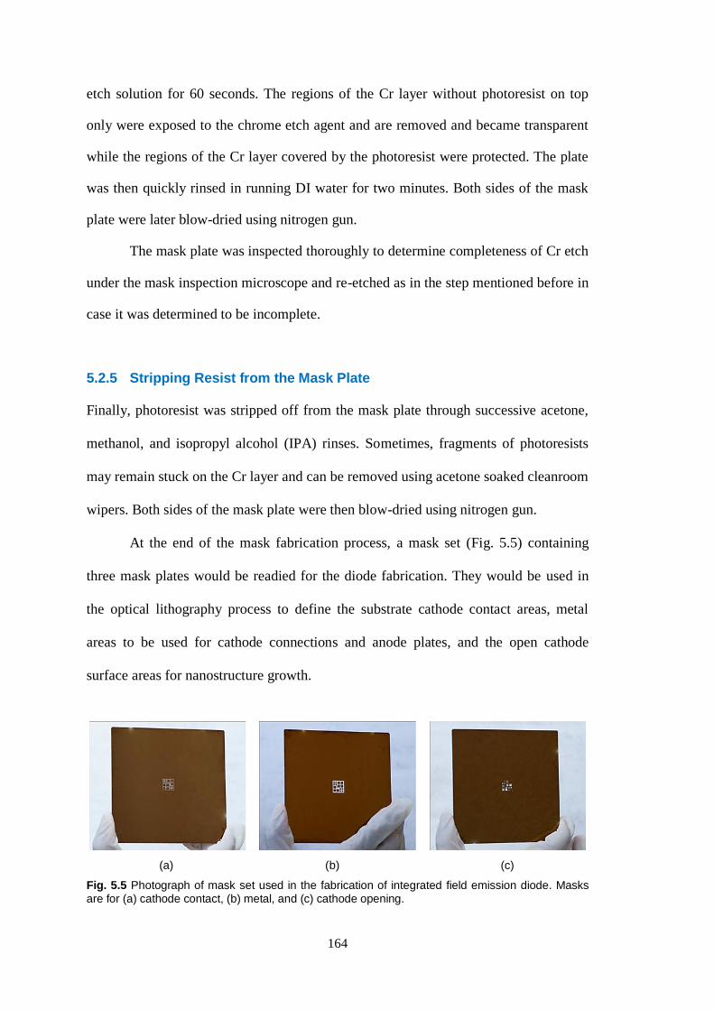
164
etch solution for 60 seconds. The regions of the Cr layer without photoresist on top
only were exposed to the chrome etch agent and are removed and became transparent
while the regions of the Cr layer covered by the photoresist were protected. The plate
was then quickly rinsed in running DI water for two minutes. Both sides of the mask
plate were later blow-dried using nitrogen gun.
The mask plate was inspected thoroughly to determine completeness of Cr etch
under the mask inspection microscope and re-etched as in the step mentioned before in
case it was determined to be incomplete.
5.2.5 Stripping Resist from the Mask Plate
Finally, photoresist was stripped off from the mask plate through successive acetone,
methanol, and isopropyl alcohol (IPA) rinses. Sometimes, fragments of photoresists
may remain stuck on the Cr layer and can be removed using acetone soaked cleanroom
wipers. Both sides of the mask plate were then blow-dried using nitrogen gun.
At the end of the mask fabrication process, a mask set (Fig. 5.5) containing
three mask plates would be readied for the diode fabrication. They would be used in
the optical lithography process to define the substrate cathode contact areas, metal
areas to be used for cathode connections and anode plates, and the open cathode
surface areas for nanostructure growth.
(a) (b) (c)
Fig. 5.5 Photograph of mask set used in the fabrication of integrated field emission diode. Masks are for (a) cathode contact, (b) metal, and (c) cathode opening.
165
5.2.6 Precautions
All laboratory safety procedures, such as use of gloves, visor and apron must be
followed during the photomask plate development and chrome etch steps as the
alkaline developer and acidic chrome etch solutions can cause severe burns and
blindness. The entire mask fabrication process must be carried out in the yellow room
to avoid unwanted exposure of photoresist on the mask.
5.3 Process Integration
The individual well-established CMOS-processes such as oxidation, photolithography,
etching, ion implantation, metal deposition, electron beam annealing that are described
in Chapter 3 are combined in various ways (Fig. 5.1) to realize the integrated field
emission diode for the present work. Briefly, the devices were fabricated on silicon
substrate using the three masks as made by following methods described in
Section 5.2. Thermal oxide over silicon substrate was patterned and etched for the
cathode (substrate) contacts. Tungsten was deposited over the open contact areas as
well as over the oxide and was first patterned with metal cathode contact and anode
plate definition, etched and then patterned with nanostructure area definition over
anode plate and etched through both the metal and oxide to expose the underlying
silicon substrate surface. Finally, self-assembled nanostructures were formed on the
exposed silicon areas through electron beam annealing to complete the fabrication of
the field emission device.
This section describes the integrated sequence of process steps, a specific
sequence that constitutes what is called the process flow, in detail. A brief version of
the process flow with individual process recipe is included in the appendix.
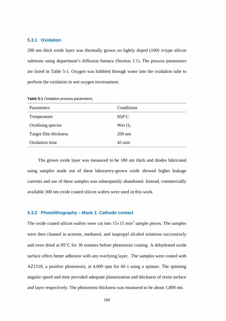
166
5.3.1 Oxidation
200 nm thick oxide layer was thermally grown on lightly doped (100) n-type silicon
substrate using department’s diffusion furnace (Section 3.1). The process parameters
are listed in Table 5-1. Oxygen was bubbled through water into the oxidation tube to
perform the oxidation in wet oxygen environment.
Table 5-1 Oxidation process parameters.
Parameters Conditions
Temperature 950C
Oxidising species Wet O2
Target film thickness 200 nm
Oxidation time 45 min
The grown oxide layer was measured to be 180 nm thick and diodes fabricated
using samples made out of these laboratory-grown oxide showed higher leakage
currents and use of these samples was subsequently abandoned. Instead, commercially
available 300 nm oxide coated silicon wafers were used in this work.
5.3.2 Photolithography – Mask 1: Cathode contact
The oxide coated silicon wafers were cut into 1515 mm2 sample pieces. The samples
were then cleaned in acetone, methanol, and isopropyl alcohol solutions successively
and oven dried at 85C for 30 minutes before photoresist coating. A dehydrated oxide
surface offers better adhesion with any overlying layer. The samples were coated with
AZ1518, a positive photoresist, at 4,000 rpm for 60 s using a spinner. The spinning
angular speed and time provided adequate planarization and thickness of resist surface
and layer respectively. The photoresist thickness was measured to be about 1,800 nm.

167
The coated resist was soft-baked at 100C for 90 s on a hot plate. This was done
to drive any residual solvent, improve adhesion of resist to the underlying layer, and
anneal the shear stresses introduced during the spin-coating [179]. The samples were
then exposed with Mask 1 for ‘cathode contact’ definition in the Karl Suss MA6 mask
aligner (Section 3.2.3). 20 s exposures were carried out in ‘hard contact’ mode with
40 m separation between the mask and the sample. The exposure time was
determined through experimentation which provided the optimum exposure for the
coated photoresist.
The sample with exposed resist was developed in the MIF300 developer solution
for 20 seconds. As described in Section 3.2.2, exposed regions of the positive
photoresist became more soluble than the unexposed regions in the developer solution
and were removed during the development process. Samples were then rinsed in
running DI water for two minutes and finally dried using a nitrogen gun. The quality
of the developed pattern depends on excellence of the initial resist application on the
sample, uniformity of resist thickness, and adequacy of pre-bake conditions, developer
chemistry and development time. The cathode contact mask, its optical exposure, and
subsequent development of photoresist are represented schematically in Fig. 5.6(a)
through Fig. 5.6(c).
Later on the samples were post-baked at 85C for 30 min. This thermal treatment
improves the photoresist adhesion to the underlying layer and its resistance control to
subsequent process steps. Photoresist thickness (height), and open area length and
width were measured by Dektak profilometer for reference.

168
Fig. 5.6 Schematic representation of process steps from cathode (substrate) contact area definition to metalization: (a) the dark-field cathode contact mask top view, (b) UV light exposure, (c) photoresist development, (d) oxide etch, (e) arsenic ion implantation, (f) resist removal, and (g) metal deposition.
5.3.3 SiO2 Etch
SiO2 areas of the samples that were then opened with patterns in photoresist were
etched in buffered HF solution, made by mixing 40 g NH4F in 10 ml 49% HF with 60
ml H2O, for six minutes 15 seconds. The wet etch procedure is described in
Section 3.3.1 The etch rate of about 1 nm/sec makes the etch time sufficient to ensure
complete removal of 300 nm thick SiO2 layer from the open areas. Height of the
removed oxide can be verified by comparing the measured height of the photoresist
and oxide layers with that of photoresist layer alone. The wet isotropic etch of SiO2
provides for improved oxide sidewall structure for coverage during metal deposition.
The outcome of the etching step is presented schematically in Fig. 5.6(d). Figure 5.7 is
an optical image of a part of a sample showing removed oxide areas.
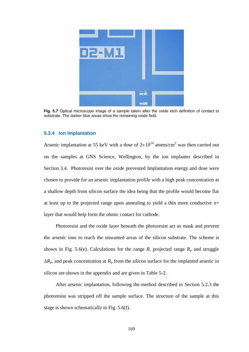
169
Fig. 5.7 Optical microscope image of a sample taken after the oxide etch definition of contact to substrate. The darker blue areas show the remaining oxide field.
5.3.4 Ion Implantation
Arsenic implantation at 55 keV with a dose of 21014
atoms/cm2 was then carried out
on the samples at GNS Science, Wellington, by the ion implanter described in
Section 3.4. Photoresist over the oxide prevented Implantation energy and dose were
chosen to provide for an arsenic implantation profile with a high peak concentration at
a shallow depth from silicon surface the idea being that the profile would become flat
at least up to the projected range upon annealing to yield a thin more conductive n+
layer that would help form the ohmic contact for cathode.
Photoresist and the oxide layer beneath the photoresist act as mask and prevent
the arsenic ions to reach the unwanted areas of the silicon substrate. The scheme is
shown in Fig. 5.6(e). Calculations for the range R, projected range Rp and struggle
Rp, and peak concentration at Rp from the silicon surface for the implanted arsenic in
silicon are shown in the appendix and are given in Table 5-2.
After arsenic implantation, following the method described in Section 5.2.3 the
photoresist was stripped off the sample surface. The structure of the sample at this
stage is shown schematically in Fig. 5.6(f).
170
Table 5-2 Calculated values of arsenic ion implantation parameters in silicon (energy = 55 keV and
dose = 21014
atoms/cm2).
Parameters Calculated values
Range, R 45 nm
Projected range, Rp 40 nm
Projected struggle, Rp 11.87 nm
Peak concentration at x = Rp 6.741019
atoms/cm3
5.3.5 Metal Deposition
Blanket deposition of 90 nm tungsten film was performed next in the Edward Auto
500 DC magnetron sputterer in the department laboratory (Section 3.5). Immediately
before the loading of the samples in the sputter chamber for the deposition, the
samples were etched for about two seconds in the buffered HF solution. The samples
were dried and quickly loaded into the sputterer chamber. This was done to minimize
the thickness of the native oxide layer that was grown on the open silicon areas by the
time. It is to be noted that native oxide growth cannot be completely eliminated in a
standard pressure process environment. DC sputtering was then carried out with
process parameters given in Table 5-3 and the result of which is outlined in
Fig. 5.6(g).
Table 5-3 Process parameters of tungsten deposition.
Parameters Values
Target W (99.99%)
Power 300W
Type DC
Process pressure 710–3
mBar
Process temperature 23C < T < 50C
Target film thickness 90 nm
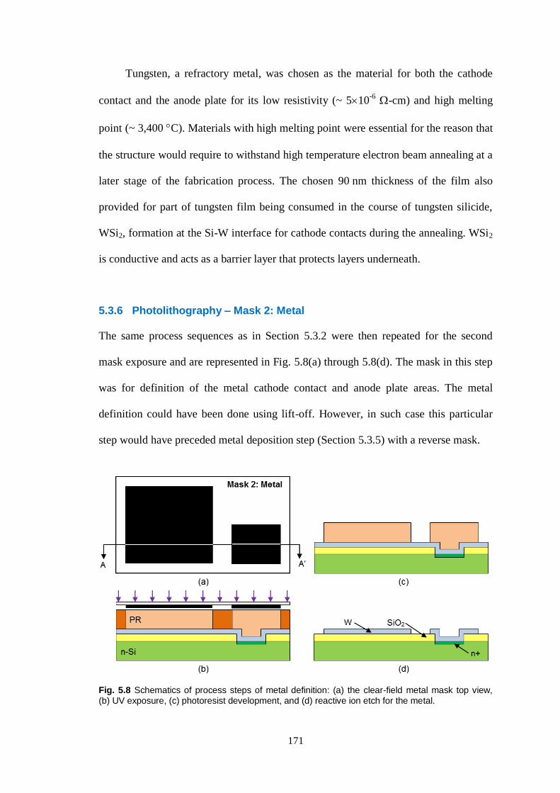
171
Tungsten, a refractory metal, was chosen as the material for both the cathode
contact and the anode plate for its low resistivity (~ 510-6
-cm) and high melting
point (~ 3,400 C). Materials with high melting point were essential for the reason that
the structure would require to withstand high temperature electron beam annealing at a
later stage of the fabrication process. The chosen 90 nm thickness of the film also
provided for part of tungsten film being consumed in the course of tungsten silicide,
WSi2, formation at the Si-W interface for cathode contacts during the annealing. WSi2
is conductive and acts as a barrier layer that protects layers underneath.
5.3.6 Photolithography – Mask 2: Metal
The same process sequences as in Section 5.3.2 were then repeated for the second
mask exposure and are represented in Fig. 5.8(a) through 5.8(d). The mask in this step
was for definition of the metal cathode contact and anode plate areas. The metal
definition could have been done using lift-off. However, in such case this particular
step would have preceded metal deposition step (Section 5.3.5) with a reverse mask.
Fig. 5.8 Schematics of process steps of metal definition: (a) the clear-field metal mask top view, (b) UV exposure, (c) photoresist development, and (d) reactive ion etch for the metal.

172
The important element in this optical lithography step is the process of
alignment of the new mask patterns with the already processed patterns on the sample
surface from the first mask. Vertical, horizontal, and angular alignment knobs of the
mask aligner were used meticulously to align specially designed mask alignment
patterns of the two involved layers as shown in the scheme in Fig. 5.9(a) and
Fig. 5.9(b), and the execution of the same in the processing step in Fig. 5.9(c). Though
enough latitude was given in the present design for misalignments, in the form of
overlap and minimum spacing in the design rule set (Section 5.2.1), issues related to
alignment may become critical in designs with smaller features and they are some
constraints to miniaturization.
Fig. 5.9 Alignment scheme in mask layout (a), and patterns after processing for masks 1 and 2 definitions on the silicon sample (b).
5.3.7 Metal Etch
Metal definition in Mask 2 was transferred to the tungsten layer from the photoresist
through reactive ion etching of the metal. The dry anisotropic etching was performed
in RIE plasma reactor (Section 3.3.2). The process parameters for the step are given in
Table 5-4.

173
Table 5-4 Process parameters for the reactive ion etching of tungsten. Some amount of SiO2 and AZ1815 were also etched during the process.
Parameters Conditions
Feed gases SF6
Flow rate 40 sccm
RF power 200 W
Etch pressure 150 mTorr
Temperature 313 K
Etch mask AZ1815
Tungsten etch rate 2.25 nm/s
SiO2 etch rate 10.45 nm/s
AZ1815 etch rate 5.76 nm/s
The RIE end point is difficult to determine and as such the RIE is required to be
appropriately timed. The etch rates are to be found through RIE characterization
involving the feed gases and etch layers to be used. A 42 s reactive ion etching was
found adequate to completely etch the tungsten layer. An incomplete etch of tungsten
would mean a short circuit of anode and cathode and must be avoided for the
fabrication of a functional device. The top view of a processed sample after the metal
definition step is shown in Fig. 510.
Fig. 5.10 Optical microscope image of a sample taken after the metal etch definition for cathode contact to substrate and anode plate.

174
5.3.8 Photolithography – Mask 3: Nanostructured area
Again, the same processes as in Section 5.3.2 were repeated but this time for the
exposure of the third and the final mask. The mask and the relevant steps of exposure
and resist development are charted in Fig. 5.11(a)-(c). This mask defined the areas on
the silicon cathode surface that would be opened through the anode plate and the oxide
where nanostructures would be grown.
Fig. 5.11 Schematic representation of process steps from nanostructure area definition to nanostructure growth: (a) the dark field ‘nanostructure area’ mask top view, (b) UV exposure, (c) resist development, (d) reactive ion etch for tungsten, (e) oxide etch to expose silicon surface, (f) photoresist removal, and (f) electron beam annealing for nanostructure growth on exposed silicon surface.
Before the exposure, the patterns from Mask 3 were aligned with the patterns
from the previous step, i.e., from Mask 2. The resultant sample after the development
of the exposed photoresist is shown in Fig. 5.11(c) (schematic) and Fig. 12 (optical
image). The samples were, at this stage, ready for the subsequent anisotropic metal
and isotropic oxide etches.

175
Fig. 5.12 Optical microscope image of a sample taken after the photoresist development with the cathode opening areas (CO) defined. CC = Cathode contact, and A = anode. The sample is ready for the successive metal and oxide etches next.
5.3.9 Metal Etch
The reactive ion etching step in Section 5.3.7 was repeated for the etching of tungsten
from areas defined as ‘cathode opening’ area on the anode plate (Fig. 5.12). These
‘cathode opening’ areas are arrays of circular and square holes to be opened through
the anode plate and oxide to reach the cathode surface. During the RIE, tungsten was
calculatedly over-etched for 5 s to ensure complete removal of the metal layer from
the defined areas. A failure to a complete removal of tungsten would make the ensuing
HF etching of the oxide layer from the ‘cathode opening’ area unattainable. The over-
etching anisotropically etched part (~ 50 nm) of the underlying oxide layer. The step is
sketched in Fig. 5.11(d).
5.3.10 SiO2 Etch
Figure 5.11(e) shows the oxides etch step (Section 5.3.3) that was repeated at this
stage. The etch time was chosen to completely etch the oxide layer to expose the
silicon surface. Photoresist was stripped off to ready the samples for the high
temperature electron beam annealing. Figure 5.11(f) shows the schematic of the
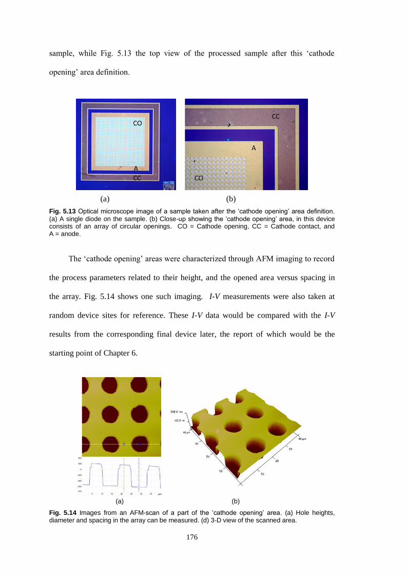
176
sample, while Fig. 5.13 the top view of the processed sample after this ‘cathode
opening’ area definition.
(a) (b)
Fig. 5.13 Optical microscope image of a sample taken after the ‘cathode opening’ area definition. (a) A single diode on the sample. (b) Close-up showing the ‘cathode opening’ area, in this device consists of an array of circular openings. CO = Cathode opening, CC = Cathode contact, and A = anode.
The ‘cathode opening’ areas were characterized through AFM imaging to record
the process parameters related to their height, and the opened area versus spacing in
the array. Fig. 5.14 shows one such imaging. I-V measurements were also taken at
random device sites for reference. These I-V data would be compared with the I-V
results from the corresponding final device later, the report of which would be the
starting point of Chapter 6.
(a) (b)
Fig. 5.14 Images from an AFM-scan of a part of the ‘cathode opening’ area. (a) Hole heights, diameter and spacing in the array can be measured. (d) 3-D view of the scanned area.
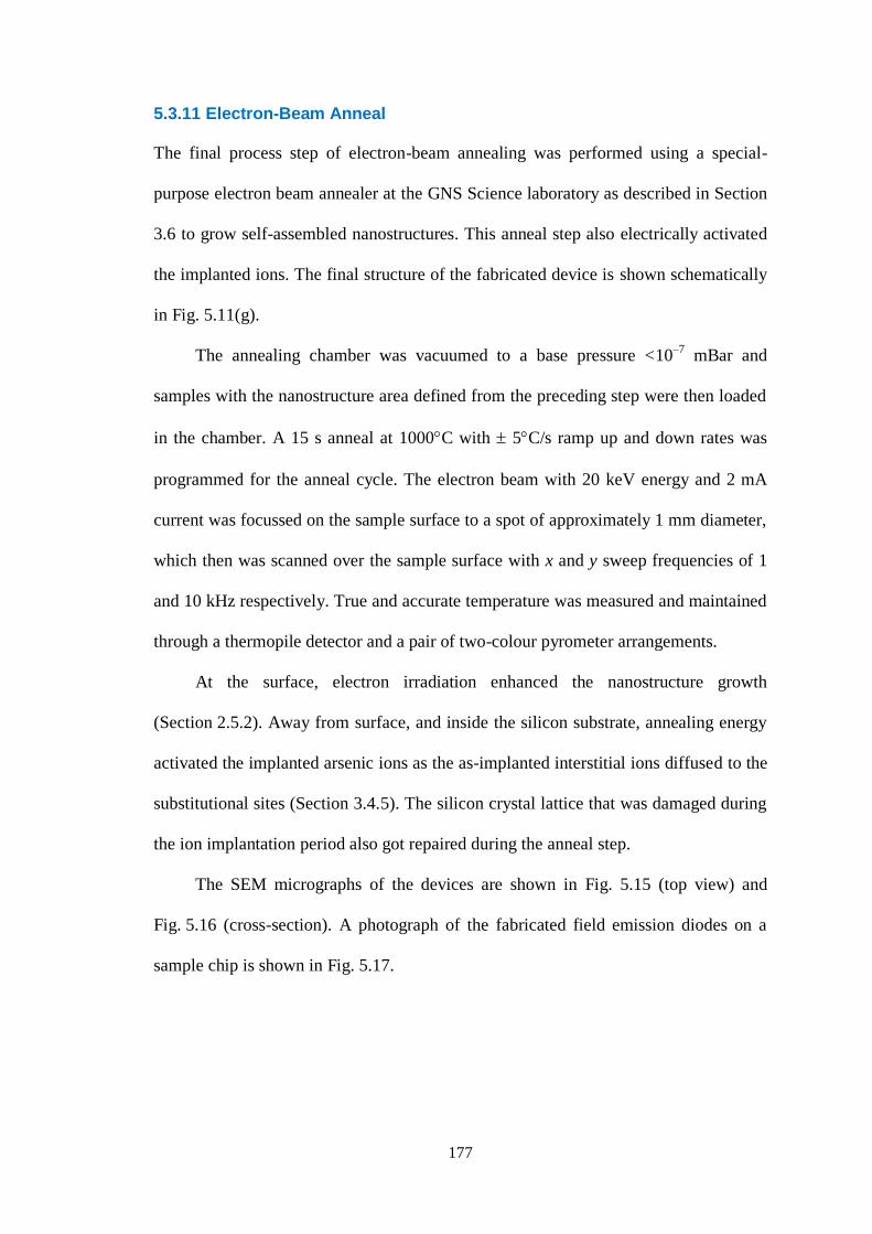
177
5.3.11 Electron-Beam Anneal
The final process step of electron-beam annealing was performed using a special-
purpose electron beam annealer at the GNS Science laboratory as described in Section
3.6 to grow self-assembled nanostructures. This anneal step also electrically activated
the implanted ions. The final structure of the fabricated device is shown schematically
in Fig. 5.11(g).
The annealing chamber was vacuumed to a base pressure <10–7
mBar and
samples with the nanostructure area defined from the preceding step were then loaded
in the chamber. A 15 s anneal at 1000C with 5C/s ramp up and down rates was
programmed for the anneal cycle. The electron beam with 20 keV energy and 2 mA
current was focussed on the sample surface to a spot of approximately 1 mm diameter,
which then was scanned over the sample surface with x and y sweep frequencies of 1
and 10 kHz respectively. True and accurate temperature was measured and maintained
through a thermopile detector and a pair of two-colour pyrometer arrangements.
At the surface, electron irradiation enhanced the nanostructure growth
(Section 2.5.2). Away from surface, and inside the silicon substrate, annealing energy
activated the implanted arsenic ions as the as-implanted interstitial ions diffused to the
substitutional sites (Section 3.4.5). The silicon crystal lattice that was damaged during
the ion implantation period also got repaired during the anneal step.
The SEM micrographs of the devices are shown in Fig. 5.15 (top view) and
Fig. 5.16 (cross-section). A photograph of the fabricated field emission diodes on a
sample chip is shown in Fig. 5.17.

178
(a)
(b)
Fig. 5.15 SEM micrographs of a processed sample (top view) showing (a) parts of field emission diodes and control capacitor, and (b) ‘cathode opening’ area array with square holes. The rounding of corners of the opened hole is evident.
Fig. 5.16 SEM micrograph of a part of a field emission diode cross-section showing the opened nanostructured cathode surface. The oxide undercut is also noticeable.
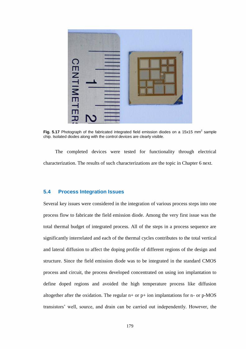
179
Fig. 5.17 Photograph of the fabricated integrated field emission diodes on a 15x15 mm2 sample
chip. Isolated diodes along with the control devices are clearly visible.
The completed devices were tested for functionality through electrical
characterization. The results of such characterizations are the topic in Chapter 6 next.
5.4 Process Integration Issues
Several key issues were considered in the integration of various process steps into one
process flow to fabricate the field emission diode. Among the very first issue was the
total thermal budget of integrated process. All of the steps in a process sequence are
significantly interrelated and each of the thermal cycles contributes to the total vertical
and lateral diffusion to affect the doping profile of different regions of the design and
structure. Since the field emission diode was to be integrated in the standard CMOS
process and circuit, the process developed concentrated on using ion implantation to
define doped regions and avoided the high temperature process like diffusion
altogether after the oxidation. The regular n+ or p+ ion implantations for n- or p-MOS
transistors’ well, source, and drain can be carried out independently. However, the
180
activation and drive of all the implanted ions were integrated in the electron beam
annealing step at the very end of the CMOS flow to achieve the desired doping profile
of the designed regions. Thus, the developed process does not offer any new thermal
cycle into the integration effort as such.
The integration involved three photolithographic mask definition steps. The
alignment of these masks with one another was critical and as such elaborate
alignment measures were considered and implemented in the fabrication process as
described in Section 5.3.6.
In this process tungsten was used as both anode plate and connections to cathode
contact and defined in one photolithographic step. The refractory metal with high
melting temperature was used as the process required a high temperature annealing
after a conductive layer deposition step. Polysilicon could have been a good candidate
for the anode plate. However, a process to make the polysilicon layer conductive and
another to define the plate, i.e., one more photomask and its photolithographic
definition step, would have been necessitated.
Lift-off was considered as metal definition step but was not used to avoid issues
related to metal adhesion to the substrate (cathode contact) and the oxide (anode
plate). Instead reactive ion etching was used which ensured good adhesion of metal to
the required regions.
The device isolation was also considered; p- or n- type isolation wells could
have been designed. However, the process would have required high energy ion
implantation or long thermal diffusion cycles. In absence of access to high energy ion
implanter and to avoid introduction of new thermal cycles into the process flow
isolation wells were not realized in the design. These isolation wells for field emission

181
diodes can be easily incorporated in a standard CMOS process during the p- or n-well
definition for the transistors.
All other minor issues raised during the implementation of the individual process
steps were adequately addressed during the respective steps. Finally, complete field
emission diodes on silicon chips were realized, which were then ready for electrical
characterization.
5.5 Summary
This chapter described how the various individual processes were integrated together
in sequence to completely realize a field emission diode in a standard CMOS process
flow. The process flow integrated oxidation, photolithographic definition, etching, ion
implantation, and electron beam annealing. Though initial experiments included in-
house oxidation, the process was later discarded in favour of commercially available
oxide coated wafers.
The process comprised three photomasks: cathode contact, metal, and cathode
opening to define as the names suggest the cathode contact, metal and cathode opening
in three different photolithographic exposure steps. Both isotropic wet HF etch for
oxide and anisotropic reactive ion etch for metal were used. Low energy ion
implantation was used to make the implanted contact region more conductive.
The incorporation of self-assembled silicon nanostructures as emitting sites on
the cathode surface of the device was fairly straight in the developed CMOS process.
This was achieved in the electron beam annealing step at the end of the process cycle.
In this one cycle three desired effects were realized – the silicon nanostructures were
grown as they self-assemble, implanted ions were driven to the desired profile, and as-

182
implanted interstitial ions diffused to the substitutional sites and got electrically
activated.
The fabricated diodes are the subject of electrical characterization next.

183
Chapter 6
CHARACTERIZATION OF INTEGRATED FIELD
EMISSION DIODES
In Chapter 5 the fabrication of CMOS-process integrated field emission devices using
cathodes with self-assembled silicon nanostructures as emitting sites was reported.
These devices we fabricated in order to utilize the mature silicon process technology to
develop low voltage vacuum microelectronic devices that would exhibit high current
density. The ultimate goal is to integrate both solid-state CMOS devices and vacuum
microelectronic devices in the same chip that can be powered by a single low voltage
source and offer the good from both worlds – solid-sate and vacuum technologies. In
that line, one of the objectives of this research was to study experimentally the
properties and emission characteristics of the fabricated diodes, and compare them
with other vacuum microelectronic devices, which is the focus of this chapter.
The emission characteristics of the fabricated diodes were analysed to determine
and examine physics of different current transport mechanisms at various electric field
regimes. This characterization and its understanding are essential to advance the
design, fabrication, and future research of these devices. Effective barrier height, field

184
conversion factor (indicating extent of field enhancement), and electron emitting area
at the point where Fowler-Nordheim field emission starts to dominate over Schottky
emission were found using a new unified approach. The approach calls for solving
extracted current equations from original Schottky and Fowler-Nordheim emissions
simultaneously, and the techniques for performing these analyses are described here..
Some parts of the characterization results reported in this chapter were presented
orally in the 2010 Conference on Optoelectronic and Microelectronic Materials and
Devices (COMMAD 2010) held in Canberra, Australia, 12-15 December 2010 [178].
The deviation of Fowler-Nordheim behaviour observed at high electric field was
reported at the Fifth International Conference on Advanced Materials and
Nanotechnology (AMN-5) held in Wellington, New Zealand, 7-11 February 2011
[180].
6.1 Experimental setup
Electrical measurements were carried out in an air ambient at room temperature and
pressure inside a shielded probe station using a Hewlett Packard HP 4155A parameter
analyser with the experimental setup shown schematically in Fig. 6.1. Justification for
measuring in an air ambient is as follows.
Theoretically, at room temperature and atmospheric pressure, an electron may be
considered to be travelling in a vacuum if its trajectory in air from emitter to collector
is smaller than 0.35 m, which is the value of limiting electron mean free path for
collision with residual nitrogen gas molecules in air [32]. In addition, the highest
voltage that can be applied to the anode without ions being formed in an air
environment at room temperature and atmospheric pressure was reported to be 12.5 V,

185
the value being the first ionizing potential of residual oxygen gas molecules [32].
Under these circumstances, the fabricated devices with cathode-anode separation of
300 nm would behave as vacuum devices in the course of the planned electrical
measurements. Maximum voltage applied to the anode was limited to 5 V and, under
such conditions, repeatable current-voltage characteristics were obtained indicating
that any ion-induced device degradation was minimal.
Fig. 6.1 The schematic of the electrical measurement setup. DUT is in a die that is placed over the probe station stage.
Figure 6.2 (a) shows the photograph of the test station. There are twelve devices
and three control sites in a single die (Section 5.1, Fig. 6.2(b)), which is placed on the
probe station. The built-in tungsten contacts for the cathode and the anode for the
individual devices and control sites are accessible on the surface of the die and are
probed using two sharp stainless steel needle probes. A microscope that magnifies the
structures on the die surface from the top is used to make precise contacts between
electrodes and probes. Both the cathode and the anode are connected to HP 4155A’s
source measure unit (SMU), which sources the anode with voltage, V, connects
cathode to ground, and measures the current, I, between the electrodes. Currents were
measured against voltage sweeps, recorded and analysed to characterize the emission
phenomenon at different field regimes.

186
Fig. 6.2 (a) A photograph showing the experimental setup for device characterization. The characterization was performed in air ambient at room temperature and atmospheric pressure. Nevertheless, the device operates as if it is in vacuum environment. (b) Fabricated devices on a single chip.
6.2 Origin of significant current
Electrical measurements were undertaken both before and after the Electron Beam
Annealing (EBA) step. It is to be noted that EBA (Section 5.3.11) was the step when
self-assembled nanostructures were formed over the open cathode surface areas of
silicon substrate as designed. Significant currents were detected during electrical
measurements of the completely fabricated devices. Results from a typical field
emission diode are shown as normal current-voltage (I-V) plot in Fig. 6.3 and as semi-
log I-V plot in Fig. 6.4. Currents measured before the EBA steps are also plotted in
these figures.
The difference in current magnitudes before and after EBA is apparent in
Fig. 6.3 and more so in Fig. 6.4. Forward current after the formation of self-assembled
nanostructures was in the mA range for forward voltages above 2 V and ~109 times
than that of before these nanostructures were formed. Additionally, when after EBA
forward and reverse currents at 1 V were considered, a rectification ratio of ~103 was
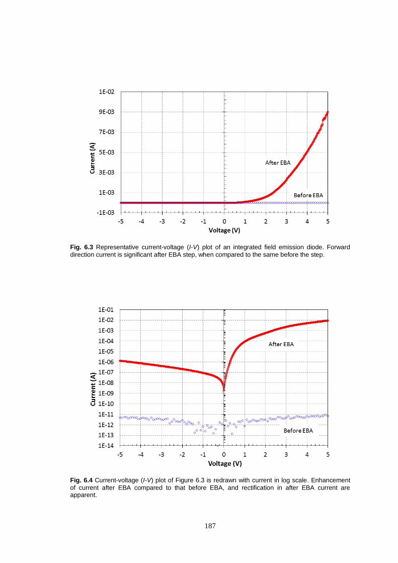
187
Fig. 6.3 Representative current-voltage (I-V) plot of an integrated field emission diode. Forward direction current is significant after EBA step, when compared to the same before the step.
Fig. 6.4 Current-voltage (I-V) plot of Figure 6.3 is redrawn with current in log scale. Enhancement of current after EBA compared to that before EBA, and rectification in after EBA current are apparent.

188
obtained. However, there was no such rectification seen for currents before EBA when
currents remained in the pA range in both bias directions.
In addition, current enhancement was not observed after EBA in control devices
(Fig. 6.5). These are the devices where no open cathode surface areas were defined to
allow formation of self-assembled nanostructures during the EBA step. These control
devices continued to register insignificant currents similar to the currents recorded
before EBA. All these observations in control devices indicate that the leakage current
between the electrodes through isolation oxide layer is negligible and therefore to
point that self-assembled nanostructures are the source of origin of current in these
devices rather than any electrically-active defects that may have been introduced into
the oxide during the EBA step. In the following sections the nature of the currents in
these devices are probed, detailed, and characterized.
Fig. 6.5 Current-voltage (I-V) plots of a control device before and after EBA showing currents in the pA range for a -5 V to 5 V sweep across its electrodes.
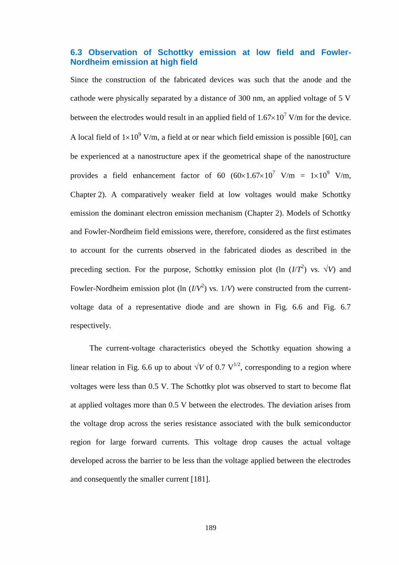
189
6.3 Observation of Schottky emission at low field and Fowler-Nordheim emission at high field
Since the construction of the fabricated devices was such that the anode and the
cathode were physically separated by a distance of 300 nm, an applied voltage of 5 V
between the electrodes would result in an applied field of 1.67107 V/m for the device.
A local field of 1109 V/m, a field at or near which field emission is possible [60], can
be experienced at a nanostructure apex if the geometrical shape of the nanostructure
provides a field enhancement factor of 60 (601.67107 V/m = 110
9 V/m,
Chapter 2). A comparatively weaker field at low voltages would make Schottky
emission the dominant electron emission mechanism (Chapter 2). Models of Schottky
and Fowler-Nordheim field emissions were, therefore, considered as the first estimates
to account for the currents observed in the fabricated diodes as described in the
preceding section. For the purpose, Schottky emission plot (ln (I/T2) vs. V) and
Fowler-Nordheim emission plot (ln (I/V2) vs. 1/V) were constructed from the current-
voltage data of a representative diode and are shown in Fig. 6.6 and Fig. 6.7
respectively.
The current-voltage characteristics obeyed the Schottky equation showing a
linear relation in Fig. 6.6 up to about V of 0.7 V1/2
, corresponding to a region where
voltages were less than 0.5 V. The Schottky plot was observed to start to become flat
at applied voltages more than 0.5 V between the electrodes. The deviation arises from
the voltage drop across the series resistance associated with the bulk semiconductor
region for large forward currents. This voltage drop causes the actual voltage
developed across the barrier to be less than the voltage applied between the electrodes
and consequently the smaller current [181].

190
Fig. 6.6 Schottky emission plot of current-voltage data for a fabricated device in 0-5V range. Linear
region is evident for V below 0.7 V1/2
, a V value that corresponds to a voltage of 0.5 V.
Fig. 6.7 Fowler-Nordheim plot of current-voltage data for a fabricated device in 0-5V range.

191
In Fig. 6.7, at low voltages, the measured data did not follow the Fowler-
Nordheim linear relationship between ln (I/V2) and 1/V which expected to provide a
negative slope. Also for the Fowler-Nordheim plot, since the abscissa was plotted as
1/V, data for high voltage/field region were consolidated in the left side of the figure.
To decide on the true character of the emission current, the Fowler-Nordheim
data, therefore, were re-plotted in Fig. 6.8 for 1-5 V range. Figure 6.8 shows initial
linear fit to Fowler-Nordheim emission behaviour at 1/V < 1 Volt-1
, i.e., where
voltages > 1 V. However, strong deviation from Fowler-Nordheim emission behaviour
is observed in voltages greater than 2.5V (1/V < 0.4 V-1
).
Fig. 6.8 Redrawn Fowler-Nordheim plot of Fig. 6.7 for 1-5V range. Deviation from linear behaviour observed at higher voltage.
From Fig. 6.6 to Fig. 6.8, it can be concluded that at low voltages, and therefore
low electric field, the dominant mechanism of current transport is Schottky emission.
Fowler-Nordheim emission constitutes the current at high voltage, i.e., at high electric
192
field. It is also noted that at still higher voltage or electric field, the emission current
deviated from the Fowler-Nordheim behaviour.
6.4 Extraction of parameters - theory and results
The parameters of interest – emitting area A, local field conversion factor , and
effective barrier height eff – were extracted from using the current equations that
represented the dominant current mechanisms at low and high fields. Schottky
emission was observed to dominate current behaviour at low fields and Fowler-
Nordheim emission at high fields as detailed in Section 6.3. Independent equations
were developed for the parameters from Schottky and Fowler-Nordheim current
equations. These equations when extended beyond their respective observed field
limits – upward for Schottky emission and downward for Fowler-Nordheim emission
– and solved simultaneously provide values for parameters at a field where Schottky
emission and Fowler-Nordheim emission are equal.
6.4.1 Theory for extraction of parameters
The Schottky emission equation [182] for current can be written as Equation (6.1)
(
√
) (6.1)
where A* is the Richardson constant and is given by Equation (6.2) as below
(6.2)

193
The local field conversion factor, c, is given by and has a unit of cm-1
.
Explanation and values of all other variables and constants used in the equations in
this chapter are listed in Table 6.1.
The permittivity of the semiconductor replaced the free-space permittivity in
Eq. (6.1) as appropriate for the metal-semiconductor system. It should be noted that in
general may be different from semiconductor static permittivity if, during the
emission process, the electron transit time from the metal-semiconductor interface to
the barrier maximum is shorter than the dielectric relaxation time in which case the
semiconductor medium is unable to be polarized. However, for silicon, the value of
is found to be approximately same as its static permittivity [183].
Table 6.1 Explanation of parameters for Equations used in Chapter 6.
Description Symbol Value Unit
Effective mass of electron (in silicon) m* 0.98m0 kg
Electron rest mass m0 9.109510-29
kg
Planck’s constant h 6.62610-34
m2kgs
-1
Emitting area A cm2
Effective barrier height eV
Local field conversion factor cm-1
Absolute temperature T 298 K
Electronic charge q 1.60210-19
C
Boltzmann constant k 1.3810-23
m2kgs
-2K
-1
Permittivity of the semiconductor (silicon) 11.98.85410-14
Fcm-1
194
Equation (6.1) can be rewritten as
( )
√
√
(6.3)
The intercept of the Schottky emission fit of linear region of Eq. (6.3) i.e.,
(
) vs. √ plot provides a relation for A and eff,
(6.4)
The Fowler-Nordheim current, IFN can be simplified as in Eq. (6.5) when the
height of the barrier is expressed in terms of effective barrier height eff,
(
) (6.5)
Equation (6.5) can also be rewritten as
( )
(
) (6.6)
The slope and intercept of the linear ln (
) vs.
fit of Eq. (6.6) gives two
equations relating A, , and eff :
(6.7)
and
( ) (6.8)
Equations (6.4), (6.7), and (6.8) can be solved simultaneously to yield eff, A, and .

195
6.4.2 Results from parameter extraction
Representative Schottky emission plot in 0.1-0.5 V range, Fowler-Nordheim plot for
1-2 V range, and respective linear fits are shown in Figures 6.9 and 6.10. Extracted
values from the measured data are enumerated in Table 6.2. The average values of the
local field conversion factor, , the extracted barrier height, eff, and the emitting
area, A were found to be about 3.3106 cm
-1, 0.28 eV, and 1.410
-11 cm
2. The
respective uncertainty in the extracted average value for a 5% uncertainty in
determining the slopes of the linear fits of a particular experimental data set in the
voltage ranges of interest is also noted in Table 6.2. The significance of the extracted
values is as follows.
Local field conversion factor, , is a function of emitter tip radius of curvature
and electrode spacing. The extracted relates to an average field enhancement of up
to 100 times (i.e., field enhancement factor, 100 from Eq. (2.29): ) at
the tips of the nanostructures that made up the device cathode (electrode separation is
300 nm). This is a significant field enhancement and means that, e.g., while the
applied field is 3.33104 Vcm
-1 for an applied bias of 1 V between the electrodes, the
actual local field experienced at the nanostructure apex would be 3.3106 Vcm
-1
because of its radius of curvature. Field emission from the nanostructure apex starts to
become the dominant contributor in current transport even at this low applied voltage
of 1 V.
The effective barrier height, eff, of 0.28 eV extracted for the devices is
considerably lower than the silicon electron affinity, , of 4.05 eV. eff found at
the onset of field emission from these nanostructures is in line with the results from
the Conductive Atomic Force Microscopy (C-AFM) study described in Chapter 4. As
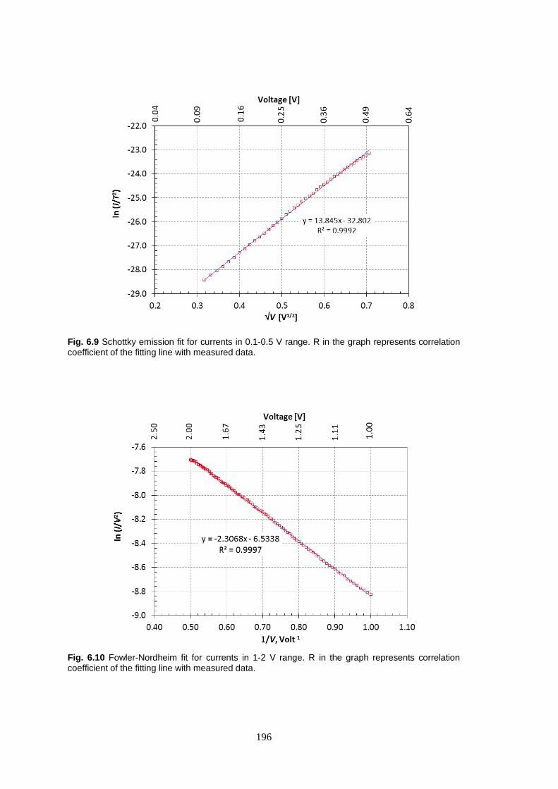
196
Fig. 6.9 Schottky emission fit for currents in 0.1-0.5 V range. R in the graph represents correlation coefficient of the fitting line with measured data.
Fig. 6.10 Fowler-Nordheim fit for currents in 1-2 V range. R in the graph represents correlation coefficient of the fitting line with measured data.

197
the nanostructure apex and the probe tip was separated by only 15 Å of native
oxide, the applied field itself in the C-AFM study was stronger and therefore a
still lower effective barrier height (0.17 - 0.19 eV) resulted upon even a moderate field
enhancement in the previous study. Because of a comparatively higher effective
barrier height for the individual nanostructures in the device arrangement, the current
in the devices would be less from Schottky emission (and that too in the essentially
off-state low voltage region) and more from tunnelling, i.e., from Fowler-Nordheim
field emission, which would predominate at high forward bias voltage.
Table 6.2 Extracted emission parameter values.
Parameter Extracted value
average
Uncertainty in
extracted value
Effective barrier height, eff 0.28 eV 4%
Local field conversion factor, 3.3106 cm
-1 8%
Emitting area, A 1.410-11
cm2 17%
The extracted total emitting area, A, comprises of the sum of all the individual
emitting site areas, i.e., the nanostructure tip areas. We recall from Chapter 2 and
Eq. (2.27) that the electric field, (
) where h is the height, r the radius of
a whisker, and F0 the flat parallel-plane electric field [80]. We also recall that the
factor (
) is known as the field enhancement factor, . Since the individual
nanostructures were subjected to the overall field enhancement individually, we argue
the relation can be applied to and should hold good for individual nanostructures on
the cathode surface. With a known field enhancement factor (~100) and height h
(~10 nm) for a nanostructure, we now, therefore, can find the radius of the emitting
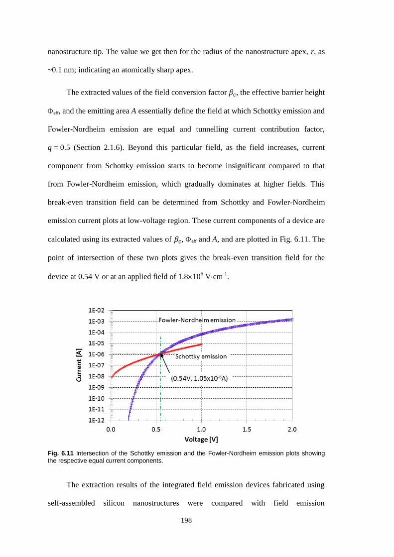
198
nanostructure tip. The value we get then for the radius of the nanostructure apex, r, as
~0.1 nm; indicating an atomically sharp apex.
The extracted values of the field conversion factor , the effective barrier height
eff, and the emitting area A essentially define the field at which Schottky emission and
Fowler-Nordheim emission are equal and tunnelling current contribution factor,
q = 0.5 (Section 2.1.6). Beyond this particular field, as the field increases, current
component from Schottky emission starts to become insignificant compared to that
from Fowler-Nordheim emission, which gradually dominates at higher fields. This
break-even transition field can be determined from Schottky and Fowler-Nordheim
emission current plots at low-voltage region. These current components of a device are
calculated using its extracted values of , eff and A, and are plotted in Fig. 6.11. The
point of intersection of these two plots gives the break-even transition field for the
device at 0.54 V or at an applied field of 1.8106 Vcm
-1.
Fig. 6.11 Intersection of the Schottky emission and the Fowler-Nordheim emission plots showing the respective equal current components.
The extraction results of the integrated field emission devices fabricated using
self-assembled silicon nanostructures were compared with field emission
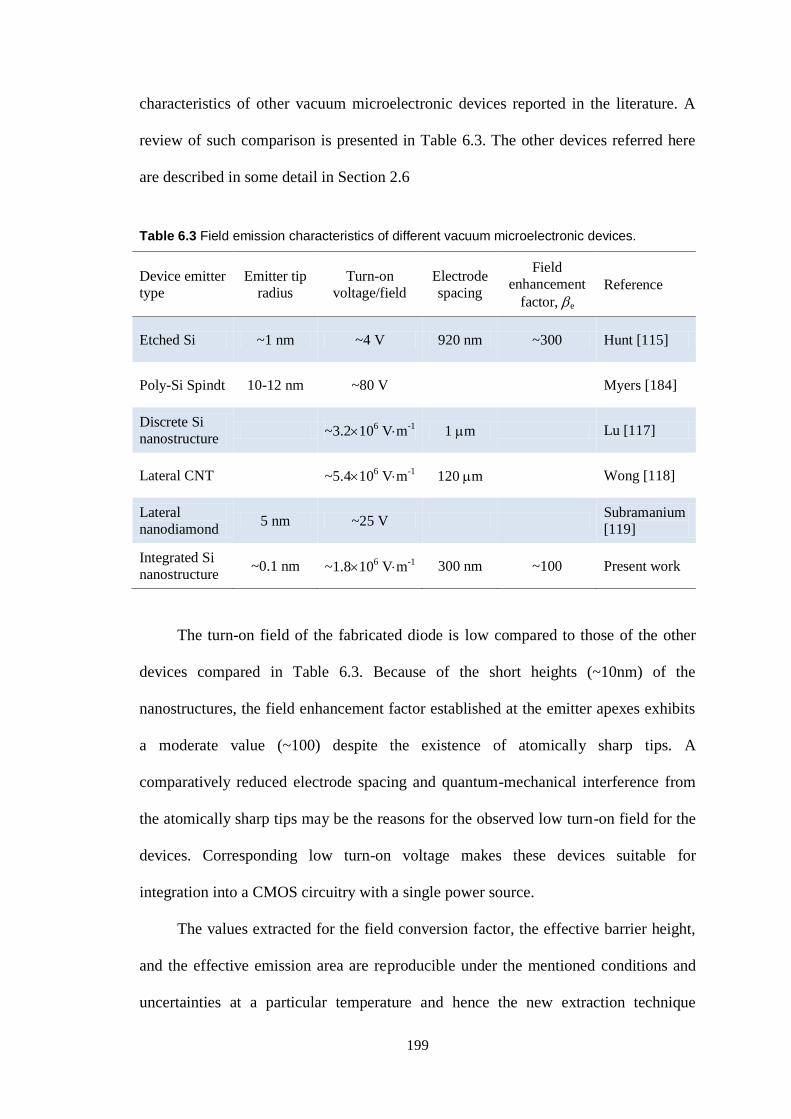
199
characteristics of other vacuum microelectronic devices reported in the literature. A
review of such comparison is presented in Table 6.3. The other devices referred here
are described in some detail in Section 2.6
Table 6.3 Field emission characteristics of different vacuum microelectronic devices.
Device emitter
type
Emitter tip
radius
Turn-on
voltage/field
Electrode
spacing
Field
enhancement
factor, e
Reference
Etched Si ~1 nm ~4 V 920 nm ~300 Hunt [115]
Poly-Si Spindt 10-12 nm ~80 V Myers [184]
Discrete Si
nanostructure ~3.210
6 Vm
-1 1 m Lu [117]
Lateral CNT ~5.4106 Vm
-1 120 m Wong [118]
Lateral
nanodiamond 5 nm ~25 V
Subramanium
[119]
Integrated Si
nanostructure ~0.1 nm ~1.810
6 Vm
-1 300 nm ~100 Present work
The turn-on field of the fabricated diode is low compared to those of the other
devices compared in Table 6.3. Because of the short heights (~10nm) of the
nanostructures, the field enhancement factor established at the emitter apexes exhibits
a moderate value (~100) despite the existence of atomically sharp tips. A
comparatively reduced electrode spacing and quantum-mechanical interference from
the atomically sharp tips may be the reasons for the observed low turn-on field for the
devices. Corresponding low turn-on voltage makes these devices suitable for
integration into a CMOS circuitry with a single power source.
The values extracted for the field conversion factor, the effective barrier height,
and the effective emission area are reproducible under the mentioned conditions and
uncertainties at a particular temperature and hence the new extraction technique
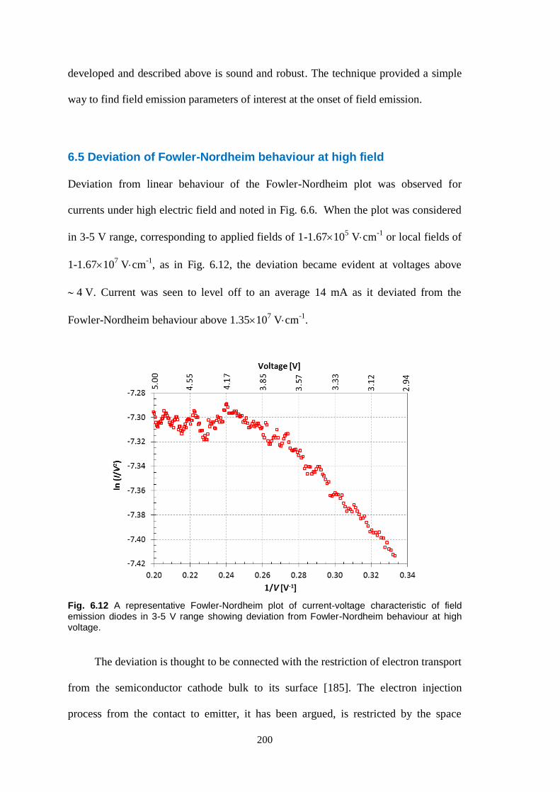
200
developed and described above is sound and robust. The technique provided a simple
way to find field emission parameters of interest at the onset of field emission.
6.5 Deviation of Fowler-Nordheim behaviour at high field
Deviation from linear behaviour of the Fowler-Nordheim plot was observed for
currents under high electric field and noted in Fig. 6.6. When the plot was considered
in 3-5 V range, corresponding to applied fields of 1-1.67105 Vcm
-1 or local fields of
1-1.67107 Vcm
-1, as in Fig. 6.12, the deviation became evident at voltages above
4 V. Current was seen to level off to an average 14 mA as it deviated from the
Fowler-Nordheim behaviour above 1.35107 Vcm
-1.
Fig. 6.12 A representative Fowler-Nordheim plot of current-voltage characteristic of field emission diodes in 3-5 V range showing deviation from Fowler-Nordheim behaviour at high voltage.
The deviation is thought to be connected with the restriction of electron transport
from the semiconductor cathode bulk to its surface [185]. The electron injection
process from the contact to emitter, it has been argued, is restricted by the space
201
charge of electrons in the cathode’s bulk. Current saturation in n-type silicon
nanostructures from space charge limited conduction has also been confirmed by
Lu et al. [117]. Again, theoretically, the band gap of the semiconductor presents
another source for the electron supply limitation. In a semiconductor, as mentioned in
Section 2.2.1 (Fig. 2.28) while discussing supply of electrons, field emission can occur
from the conduction as well as from the valence band; emission from the valence band
requires a higher electric field [58]. The field emission starts from the conduction band
at a comparatively low field and initially the supply of electrons is sufficient to
maintain the increasing current with increasing field. However, as the field continues
to increase, eventually conduction band emission saturates as it becomes electron
supply limited due to the finite dopant concentration in the conduction band. And it is
not until the field becomes high enough to present a thinner barrier at the valence band
level for electron emission from the valence band, the saturation regime continues to
hold. Ding et al. [186] provided a velocity saturation model for electron emission
where small tip radius and low electron concentration in conduction band were
thought as key factors in determining the occurrence of the saturation.
6.6 Summary
In summary, we have observed four regions in the forward bias operation of the
fabricated field emission diode: cut-off, mixed-mode, electron transmission controlled
(Fowler-Nordheim), and electron supply controlled regions. In the cut-off region, the
current data agrees with the Schottky emission theory. In the mixed-mode region the
tunnelling of electrons from near and at Fermi level starts to take effect. At the end of
the mixed-mode region the Schottky emission model deviates and the experimental

202
data agrees well with the electron transmission related Fowler Nordheim theory.
However, at higher bias voltage current is limited by electron supply and current
saturation occurs.
We have also extracted effective barrier height eff, local field conversion factor
, and total emitting area A for the field emission diode using independent equations
extracted from Schottky and Fowler-Nordheim emission current equations. Values for
these parameters, now known, would help us to understand and approximate the
current transport mechanisms in the fabricated field emission diode. In addition, from
the extracted local field conversion factor, we have found that the field emission is
from the atomically sharp nanostructure sites.
203
Chapter 7
MODELLING AND SIMULATION OF
FIELD ENHANCEMENT
A model is a simplified physical and mathematical representation of a real or a
theoretical system, while a simulation is the operation or execution of the model to aid
observation of the interactions of the system that would not otherwise be apparent. A
simulation, therefore, can provide a good understanding of the working of a system,
predict results from the system or its variations, and help to improve the system
design. However, the quality of the results of a simulation depends on how good the
system was modelled, both geometrically and mathematically.
The modelling and simulation related to field emission from silicon
nanostructures were carried out in order to understand the phenomenon of field
enhancement due to variation in physical structure of these nanoemitters under
different conditions. Commercially available COMSOL Multiphysics [187] was used
as the finite element method (FEM) simulation package for the electrostatic modelling
and simulation. The results from these modelling and simulation studies of field
enhancement from silicon nanostructures in conductive AFM and field emission diode
systems are reported in this chapter. Validations were also performed against well-
known and standard structures. The variance between 2D in-plane and axisymmetric
simulation results was analysed. These simulations provided useful insight regarding

204
electrostatics on a macroscopic scale, for example, when applied to the optimisation of
diode geometry or modelling the electric field associated with the metal coated AFM
tip. The limitation of the simulations on the nanometre scale was evident in finding a
lower simulated field enhancement factor for nanostructures, as quantum-mechanical
effect was neglected. However, the trend of increasing field enhancement factor with
decreasing radius of nanostructure apex was established.
7.1 Electrostatics, the Finite Element Method, and COMSOL
This section briefly overviews the relevant electrostatics, and outlines the finite
element method and its implementation by COMSOL in the modelling and simulation
of approximate potential and electric field in arbitrary arrangements and shapes of
emitters and collectors along with dielectrics.
7.1.1 Poisson and Laplace Equations
The behaviour of an electrostatic field can be described by two differential
equations [188]
(7.1)
and
(7.2)
where D is the electric displacement, the charge density, and E the electric field.
Equation (7.2) is equivalent to
(7.3)
where V is the scalar potential. Also the constitutive law that describes the
macroscopic properties of the medium relates D and E by:
(7.4)

205
where is the permittivity of the medium given by , where is the
permittivity of free space and is the relative permittivity of the medium. Equations
(7.1), (7.3), and (7.4) can be combined into
( ) (7.5)
This is called the Poisson equation. In absence of a charge density in the region of
interest, the equation turns into the Laplace equation
( ) (7.6)
The Poisson or Laplace equation can be solved to find the electric potential in a
space with arbitrary electrode geometry and applied voltage between the electrodes,
from which the electric field can be determined. The space charge effects can be
neglected for low current densities and the simplified Laplace equation with relevant
Dirichlet boundary conditions can be used for the purpose. The Dirichlet boundary
condition, when imposed on a differential equation, specifies a unique and well-
behaved value the solution needs to take on the boundary of the domain [188].
Various simulation software packages, such as SPEED [189], and FIDAP [190]
had been available to solve the Poisson or the Laplace equation in the past. Recently,
the finite volume method has also been used for the calculation of electrostatic fields
[191]. However, the commercially available COMSOL Multiphysics [187] is one of
the commonly used solvers at present and is used to obtain results reported in this
research. COMSOL Multiphysics uses the finite element method to solve the Poisson
or the Laplace equation; the method is outlined next.
7.1.2 Outline of the Finite Element Method
The finite element method (FEM) is a numerical technique that approximates a partial
differential equation (PDE) problem with a problem that has a finite number of

206
unknown parameters. This is done through discretization or breaking the original
problem space into individual finite elements or shape functions that describe the
possible forms of the approximate solution. Here, the geometry is partitioned into
small units of simple shaped mesh elements. A set of basis functions, specifies a finite
element space. The description of basis function is simplified using local coordinates.
The discretization of the equations starts with the constraints on the boundaries,
followed by constraints on the domains and the points. Discretization of the constraint
requires that the constraint must hold pointwise at the Lagrange points. The dependent
variables are approximated with functions in the chosen finite element spaces in terms
of a finite number of parameters or degrees of freedom, DOF.
The weak equation is also discretized in a similar manner. The test functions are
approximated with the same finite elements (Galerkin method). Finally, Lagrange
multipliers are discretized.
In summary, the discretization of a stationary problem is given by
( ) ( ) (7.1)
( )
where L is called the residual vector, U is the solution vector, is the Lagrange
multiplier vector, M is the constraint residual matrix, and NF is the constraints force
Jacobian matrix. The problem is then to solve the system for the solution vector U. A
detailed theoretical background of the finite element method can be found in the
seminal textbook by Olgierd Zienkiewicz and co-authors [192]. COMSOL, the
software package that incorporates the FEM to solve the Poisson or the Laplace
equation, is introduced next.
207
7.1.3 COMSOL Multiphysics for the Calculation of Electrostatic Field
The ‘electrostatics’ interface of the ‘AC/DC module’ provides the physics of the
COMSOL Multiphysics – the equations, the boundary conditions and the space
charges – for modelling the electrostatic fields, solving for the electric potential.
COMSOL combines a constitutive relationship, , where P is the electric
polarization vector to represent Gauss’s law (Eq. 7.1) in a dielectric medium as
( ) (7.6)
Different boundary conditions, such as ground, a particular electric potential,
surface charge density, dielectric shielding, terminal, distributed capacitance, zero
charge, displacement field, and periodic condition on exterior boundaries are available
in COMSOL. The relevant interface condition at interfaces between different media is
( ) (7.7)
where n is the unit normal to the surface. In the absence of surface charges s, this
condition is fulfilled by the natural boundary condition
[( ) ( ) ] ( ) (7.8)
where subscripts 1 and 2 refer to the physical quantities on either side of a boundary.
The electrostatics problem equation is built into the ‘electrostatics’ physics
interface and COMSOL converts all physics interface formulations and systems to the
weak form before solving them with the finite element method. The techniques
COMSOL uses to form the system of equations and constraints that it solves and
implications of Dirichlet boundary conditions can be found in the COMSOL reference
guide [193].
The various solvers in COMSOL, for example, the MUMPS, the SPOOLES, the
PARDISO, the GMRES solvers are examined in detail in the COMSOL reference
guide [193]. An iterative solver estimates the error of the solution while solving, and

208
when the error estimate is small enough, as determined by the convergence criterion,
COMSOL terminates the computations and returns a solution. The geometry
modelling features and the features available for meshing the geometry in COMSOL
are also described in detail also in the COMSOL reference guide [193]. The relevant
steps and considerations for the geometry modelling and the meshing are discussed in
the present text at appropriate sections.
7.2 Validation of the Simulation
The justification of using commercially available COMSOL Multiphysics package to
simulate field enhancement phenomenon encountered in the AFM study of the GNS
nanostructures (Chapter 4) and in the field emission device (Chapter 6) is elaborated in
this section. The rationalisation provided here adds to the foundation of knowledge on
our understanding of field enhancement and establishes that the 2D axisymmetric
simulation used in this study as a reasonably adequate method to explain the fields in
such circumstances.
To validate if COMSOL Multiphysics can be used to determine electric fields
from any arbitrary cathode and anode structures, a simple model of a ‘hemisphere on a
plane’ is picked as a test problem. The field enhancement factor, e, for the system is
well known and can be readily verified with the simulation result. A two-dimensional
analytical solution of the Laplace equation for such system illustrated in Fig. 7.1
would give the field enhancement factor at the hemisphere apex as e = 2 [194] and a
three-dimensional solution has e = 3 [195].
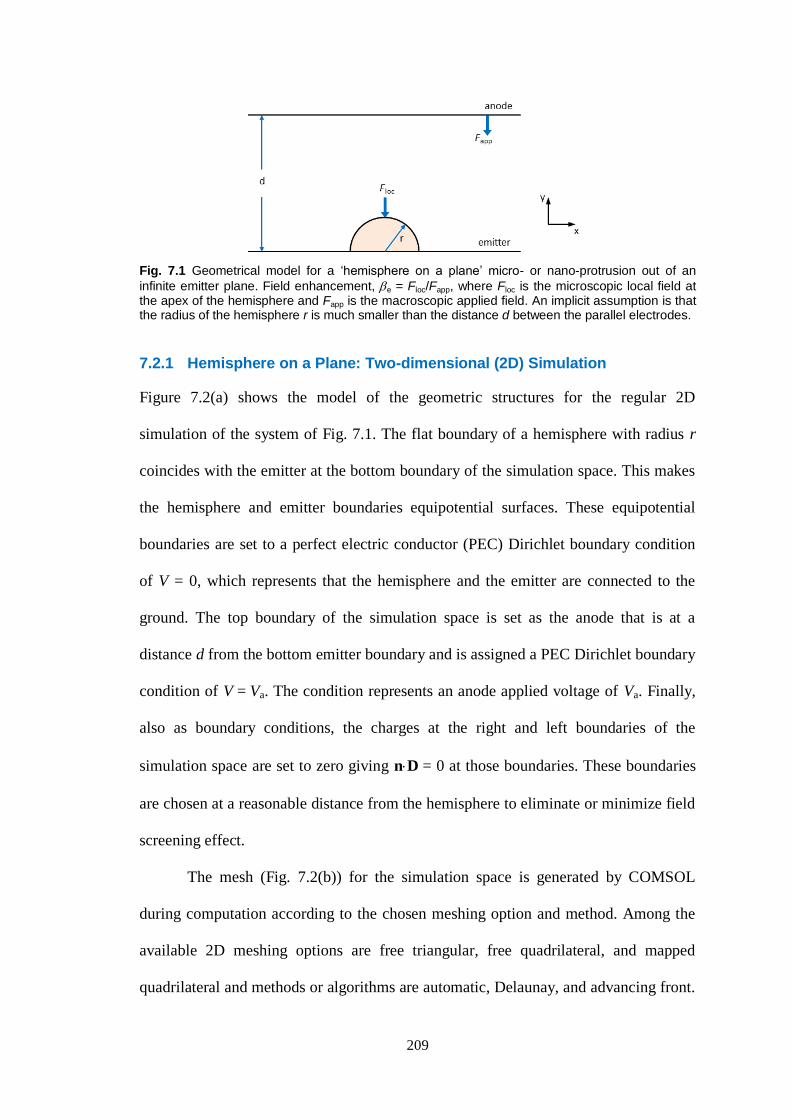
209
Fig. 7.1 Geometrical model for a ‘hemisphere on a plane’ micro- or nano-protrusion out of an
infinite emitter plane. Field enhancement, e = Floc/Fapp, where Floc is the microscopic local field at the apex of the hemisphere and Fapp is the macroscopic applied field. An implicit assumption is that the radius of the hemisphere r is much smaller than the distance d between the parallel electrodes.
7.2.1 Hemisphere on a Plane: Two-dimensional (2D) Simulation
Figure 7.2(a) shows the model of the geometric structures for the regular 2D
simulation of the system of Fig. 7.1. The flat boundary of a hemisphere with radius r
coincides with the emitter at the bottom boundary of the simulation space. This makes
the hemisphere and emitter boundaries equipotential surfaces. These equipotential
boundaries are set to a perfect electric conductor (PEC) Dirichlet boundary condition
of V = 0, which represents that the hemisphere and the emitter are connected to the
ground. The top boundary of the simulation space is set as the anode that is at a
distance d from the bottom emitter boundary and is assigned a PEC Dirichlet boundary
condition of V = Va. The condition represents an anode applied voltage of Va. Finally,
also as boundary conditions, the charges at the right and left boundaries of the
simulation space are set to zero giving nD = 0 at those boundaries. These boundaries
are chosen at a reasonable distance from the hemisphere to eliminate or minimize field
screening effect.
The mesh (Fig. 7.2(b)) for the simulation space is generated by COMSOL
during computation according to the chosen meshing option and method. Among the
available 2D meshing options are free triangular, free quadrilateral, and mapped
quadrilateral and methods or algorithms are automatic, Delaunay, and advancing front.
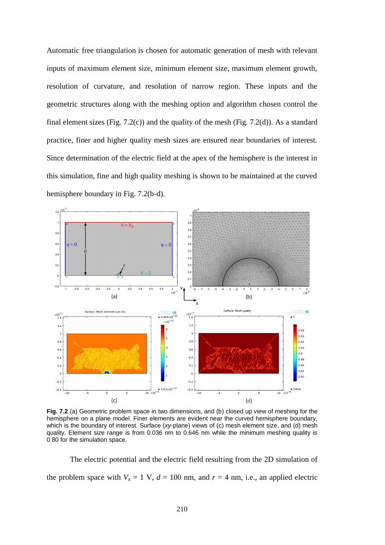
210
Automatic free triangulation is chosen for automatic generation of mesh with relevant
inputs of maximum element size, minimum element size, maximum element growth,
resolution of curvature, and resolution of narrow region. These inputs and the
geometric structures along with the meshing option and algorithm chosen control the
final element sizes (Fig. 7.2(c)) and the quality of the mesh (Fig. 7.2(d)). As a standard
practice, finer and higher quality mesh sizes are ensured near boundaries of interest.
Since determination of the electric field at the apex of the hemisphere is the interest in
this simulation, fine and high quality meshing is shown to be maintained at the curved
hemisphere boundary in Fig. 7.2(b-d).
Fig. 7.2 (a) Geometric problem space in two dimensions, and (b) closed up view of meshing for the hemisphere on a plane model. Finer elements are evident near the curved hemisphere boundary, which is the boundary of interest. Surface (xy-plane) views of (c) mesh element size, and (d) mesh quality. Element size range is from 0.036 nm to 0.646 nm while the minimum meshing quality is 0.80 for the simulation space.
The electric potential and the electric field resulting from the 2D simulation of
the problem space with Va = 1 V, d = 100 nm, and r = 4 nm, i.e., an applied electric

211
field of 1107 V/m, are shown in Fig. 7.3. The potential profile remains largely
unperturbed by the hemisphere (Fig. 7.3(a)). However, higher electric fields are
readily distinguishable around the apex of the hemisphere (Fig. 7.3(b-c)). It is to be
noted that for in-plane 2D modelling, COMSOL assumes a symmetry where the
electric potential varies only in the x and y directions and is constant in the z direction,
which implies that the electric field is tangential to the xy-plane [196].
A local electric field of 2107 V/m is extracted at the apex of the hemisphere
from the cutline drawn perpendicular to both the emitter and the anode boundary and
through the apex of the hemisphere (Fig. 7.3(d)). The corresponding field
enhancement factor, therefore, is 2, which as mentioned before is expected for
hemisphere on a plane in 2D and is the same as simulated using commercially
available SILVACO package [197].
Fig. 7.3 The simple 2D simulation results for the ‘hemisphere on a plane’ model. Surface plots showing (a) electric potential, (b) electric field, and (c) closed up view of electric field near hemisphere. (d) Electric field plot along the apex of hemisphere with 0 on the x-axis as the centre of the hemisphere.
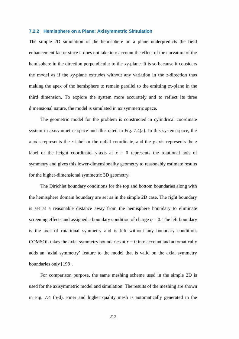
212
7.2.2 Hemisphere on a Plane: Axisymmetric Simulation
The simple 2D simulation of the hemisphere on a plane underpredicts the field
enhancement factor since it does not take into account the effect of the curvature of the
hemisphere in the direction perpendicular to the xy-plane. It is so because it considers
the model as if the xy-plane extrudes without any variation in the z-direction thus
making the apex of the hemisphere to remain parallel to the emitting zx-plane in the
third dimension. To explore the system more accurately and to reflect its three
dimensional nature, the model is simulated in axisymmetric space.
The geometric model for the problem is constructed in cylindrical coordinate
system in axisymmetric space and illustrated in Fig. 7.4(a). In this system space, the
x-axis represents the r label or the radial coordinate, and the y-axis represents the z
label or the height coordinate. y-axis at x = 0 represents the rotational axis of
symmetry and gives this lower-dimensionality geometry to reasonably estimate results
for the higher-dimensional symmetric 3D geometry.
The Dirichlet boundary conditions for the top and bottom boundaries along with
the hemisphere domain boundary are set as in the simple 2D case. The right boundary
is set at a reasonable distance away from the hemisphere boundary to eliminate
screening effects and assigned a boundary condition of charge q = 0. The left boundary
is the axis of rotational symmetry and is left without any boundary condition.
COMSOL takes the axial symmetry boundaries at r = 0 into account and automatically
adds an ‘axial symmetry’ feature to the model that is valid on the axial symmetry
boundaries only [198].
For comparison purpose, the same meshing scheme used in the simple 2D is
used for the axisymmetric model and simulation. The results of the meshing are shown
in Fig. 7.4 (b-d). Finer and higher quality mesh is automatically generated in the

213
axisymmetric space than the same generated in the simple 2D space for the same
structure.
Fig. 7.4 (a) Geometric problem space, and (b) closed up view of meshing for the hemisphere on a plane model. Finer elements are evident near the curved hemisphere boundary, which is the boundary of interest. Surface (xy-plane) views of (c) mesh element size, and (d) mesh quality. Element size range is from 0.037 nm to 0.567 nm while the minimum meshing quality is 0.86 for the simulation space.
The results of the axisymmetric simulation for the same conditions as in the
simple 2D situation are shown in Fig. 7.5. Since the axisymmetric version in
COMSOL considers the situation where the fields and geometry are axially
symmetric, the electric potential is constant in the direction, which implies that the
electric field is tangential to the rz-plane [196]. The field enhancement factor, e, at the
hemisphere apex found from the extracted local field is 3, which is the well-known
exact analytical value for the 3D ‘hemisphere on a plane’ model [195, 199]. It can,
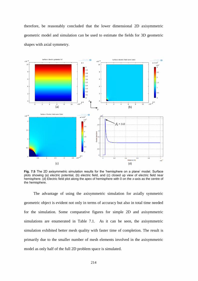
214
therefore, be reasonably concluded that the lower dimensional 2D axisymmetric
geometric model and simulation can be used to estimate the fields for 3D geometric
shapes with axial symmetry.
Fig. 7.5 The 2D axisymmetric simulation results for the ‘hemisphere on a plane’ model. Surface plots showing (a) electric potential, (b) electric field, and (c) closed up view of electric field near hemisphere. (d) Electric field plot along the apex of hemisphere with 0 on the x-axis as the centre of the hemisphere.
The advantage of using the axisymmetric simulation for axially symmetric
geometric object is evident not only in terms of accuracy but also in total time needed
for the simulation. Some comparative figures for simple 2D and axisymmetric
simulations are enumerated in Table 7.1. As it can be seen, the axisymmetric
simulation exhibited better mesh quality with faster time of completion. The result is
primarily due to the smaller number of mesh elements involved in the axisymmetric
model as only half of the full 2D problem space is simulated.

215
Table 7.1 Comparative data for simple 2D and axisymmetric simulations.
Simple 2D Axisymmetric
Number of vertex elements 7 6
Number of boundary elements 1,622 1,065
Number of elements 239,702 122,322
Minimum element quality 0.8045 0.8482
Solution time 23.715 s 14.684 s
7.2.3 Electric Field around Rounded Whisker
Once the axisymmetric simulation for ‘hemisphere on a plane’ was validated, similar
simulations were carried out for rounded whisker using the ‘hemisphere on a post’
model as illustrated in Fig. 7.6. This was done to further explore field enhancement
from sharp emitting structures and validate our method of choice for simulation of the
GNS nanostructures.
Fig. 7.6 2D geometrical model for a ‘hemisphere on a post’ micro- or nano-protrusion out of an infinite emitter plane or ‘rounded whisker’. Implicit assumption is that the height h of the protrusion is much smaller than the distance d between the parallel electrodes.
In 1964, Vibrans considered for the first time a wire-shaped body with a rounded
tip protruding out of an infinite plane and computed field around such a whisker by
numerical approximations [80]. He executed computations with an IBM 7090
computer and showed that the field enhancement at the emitting tip is given by

216
(7.9)
where h is the height and r is the radius of the rounded tip of the protrusion.
Equation (7.9) reduces to e = 3, when h = r and matches the value when
protrusion is a hemisphere as discussed, modelled, and simulated in Section 7.2.2. In
addition, for h » r, Eq. (7.9) reduces to the approximate relation
(7.10)
The axisymmetric geometric model along with boundary conditions and mesh
for a rounded whisker is shown in Fig. 7.7(a). The distance d between the emitter and
anode boundaries was kept at 100 m and the whisker tip radius r at 10 nm, which in
this case is the base radius as well. The anode voltage was set at 1,000 V implying an
applied field of 1107 V/m for the system. The axisymmetric simulations were carried
out by varying whisker height h. Fig. 7.7(b) shows result of one such simulation for
electric field near the whisker tip when h/r was 4.
Fig. 7.7 (a) Geometric problem space in axisymmetric two dimensions with mesh and Dirichlet boundary conditions, and (b) closed up view of electric field near the hemisphere on a post.
Local electric fields were extracted at the apex of the rounded whiskers and field
enhancement factors were calculated for different h/r ratios. Field enhancement factors
from the simulation, from the work of Edgcombe and Valdrè [200], and from Eq. (7.9)

217
are tabulated in Table 7.2. Table 7.2 shows that axisymmetric simulation results for
field enhancement closely matched the results of Edgcombe and Valdrè [200] and are
within about 5% of results from Eq. (7.9) when the aspect ratio h/r is below 10 and
outside 10% when the ratio is above 10.
Table 7.2 Comparison data for field enhancement factor obtained using various methods as a function of aspect ratio of a rounded whisker.
Aspect
ratio
h/r
Ftip
[V/m]
Estimate of field enhancement factor e % difference
between
simulation and
Eq. (7.1) simulation Ref. [201] Eq. (7.1)
1 3.00107 3.00 2.97 3.0 0.00
1.3 3.38107 3.38 3.35 3.3 2.48
2 4.21107 4.21 4.17 4.0 5.13
4 6.31107 6.31 6.26 6.0 5.10
11 1.27108 12.65 12.55 13.0 -2.69
31 2.84108 28.40 28.18 33.0 -13.94
101 7.70108 76.97 76.37 103.0 -25.27
301 2.02108 202.00 200.50 303.0 -33.33
7.2.4 Field Enhancement in Sharp Emitters
Electric field enhancement for emitter cones are explored in this section. The cones
are modelled as pyramids as in Fig. 7.8 in two dimensions. The sharpness of these
nanoemitters are set by a fixed radius of hemisphere on the tip of the pyramid and
variable half-angles that are made at the emitter tip by the side boundary. The
axisymmetric simulations were carried out for such nanoemitters with a radius of 1 nm
and height of 10 nm and the surface diagrams of electric fields for various half-angled
pyramids are shown in Fig. 7.9.

218
Fig. 7.8 (a) Pyramidal model of a cone emitter showing radius and half-angle at the apex. (b) 2D axisymmetric geometric setup for simulation.
Fig. 7.9 Electric field around pyramidal nanoemitter apex with half-angles (a) 45°, (b) 30°, (c) 22.5°, (d) 15°, (e) 10°, and (f) 0°.
The resultant field enhancement factors of nanoemitters with same radius for
the hemisphere at the tip and nanoemitter height followed the expected trend of
increasing field enhancement with sharpness of the approaching tip structure [21].
Field enhancement factors of the nanoemitters are plotted in Fig. 7.10 with respect to
cone half-angle.
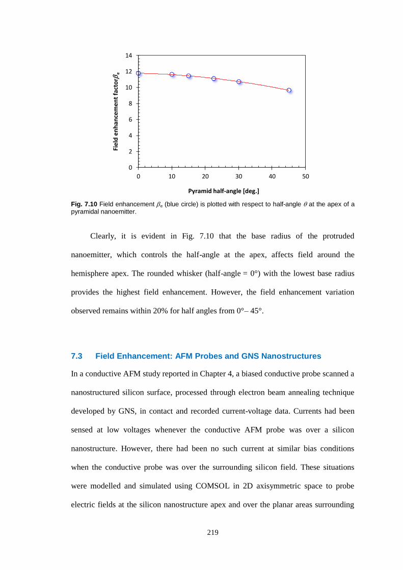
219
Fig. 7.10 Field enhancement e (blue circle) is plotted with respect to half-angle at the apex of a pyramidal nanoemitter.
Clearly, it is evident in Fig. 7.10 that the base radius of the protruded
nanoemitter, which controls the half-angle at the apex, affects field around the
hemisphere apex. The rounded whisker (half-angle = 0°) with the lowest base radius
provides the highest field enhancement. However, the field enhancement variation
observed remains within 20% for half angles from 0°– 45°.
7.3 Field Enhancement: AFM Probes and GNS Nanostructures
In a conductive AFM study reported in Chapter 4, a biased conductive probe scanned a
nanostructured silicon surface, processed through electron beam annealing technique
developed by GNS, in contact and recorded current-voltage data. Currents had been
sensed at low voltages whenever the conductive AFM probe was over a silicon
nanostructure. However, there had been no such current at similar bias conditions
when the conductive probe was over the surrounding silicon field. These situations
were modelled and simulated using COMSOL in 2D axisymmetric space to probe
electric fields at the silicon nanostructure apex and over the planar areas surrounding
0
2
4
6
8
10
12
14
0 10 20 30 40 50
Fiel
d e
nh
ance
men
t fa
cto
re
Pyramid half-angle [deg.]

220
the nanostructure in an attempt to explain such behaviour and the results are reported
in this section.
The geometric model for AFM probe tip in contact with a nanostructure is
shown in Fig.7.11. The boundary conditions with assigned biases, Va of 1 V for AFM
probe as anode and 0 V for nanostructure and substrate as cathode, are also marked.
The conductive probe has a tip radius of 25 nm and the GNS nanostructure is
atomically sharp Eifel Tower-like structure of height 10 nm. Since a thin layer of
native oxide covers the silicon nanostructure exposed in the air, the AFM probe tip and
the nanostructure separation, in effect, is about 15 Å at contact implying an applied
electric field of 0.67109 V/m for the arrangement.
Fig. 7.11 The axisymmetric geometric model showing AFM probe in contact with the GNS nanostructure apex. The small gap d represents the separation between the probe and the nanostructure due to native oxide. The necessary Dirichlet boundary conditions for simulation are also labelled.
The electric field near the apex of the nanostructure and the probe tip from the
2D axisymmetric simulation is shown in Fig. 7.12. The closeup of the arrangement
(Fig. 7.12(a)) indicates a nearly planar anode for the sharp nanostructure apex, and
subsequently the extracted electric field at the nanostructure apex is found to be
5.47109 V/m (Fig. 7.12(b)), which translates into a field enhancement factor, e, of
8.2. Since field emission requires fields in the range of 109 V/m, the result indicates
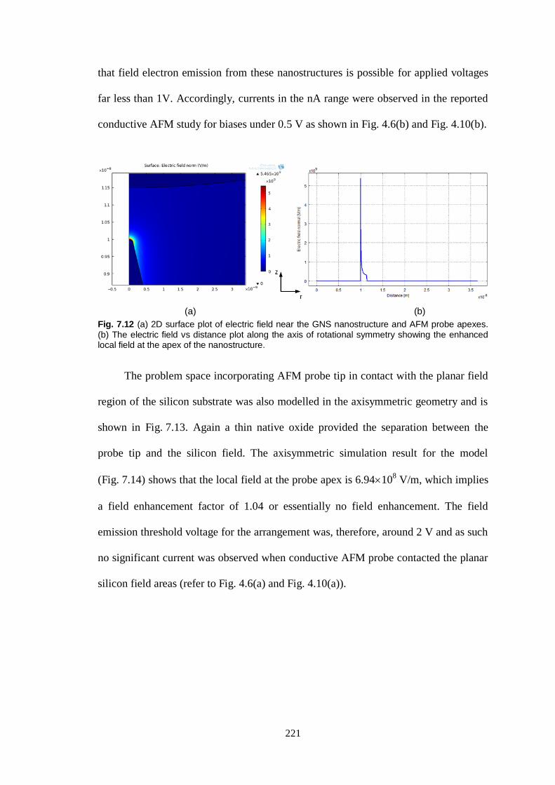
221
that field electron emission from these nanostructures is possible for applied voltages
far less than 1V. Accordingly, currents in the nA range were observed in the reported
conductive AFM study for biases under 0.5 V as shown in Fig. 4.6(b) and Fig. 4.10(b).
(a) (b)
Fig. 7.12 (a) 2D surface plot of electric field near the GNS nanostructure and AFM probe apexes. (b) The electric field vs distance plot along the axis of rotational symmetry showing the enhanced local field at the apex of the nanostructure.
The problem space incorporating AFM probe tip in contact with the planar field
region of the silicon substrate was also modelled in the axisymmetric geometry and is
shown in Fig. 7.13. Again a thin native oxide provided the separation between the
probe tip and the silicon field. The axisymmetric simulation result for the model
(Fig. 7.14) shows that the local field at the probe apex is 6.94108 V/m, which implies
a field enhancement factor of 1.04 or essentially no field enhancement. The field
emission threshold voltage for the arrangement was, therefore, around 2 V and as such
no significant current was observed when conductive AFM probe contacted the planar
silicon field areas (refer to Fig. 4.6(a) and Fig. 4.10(a)).
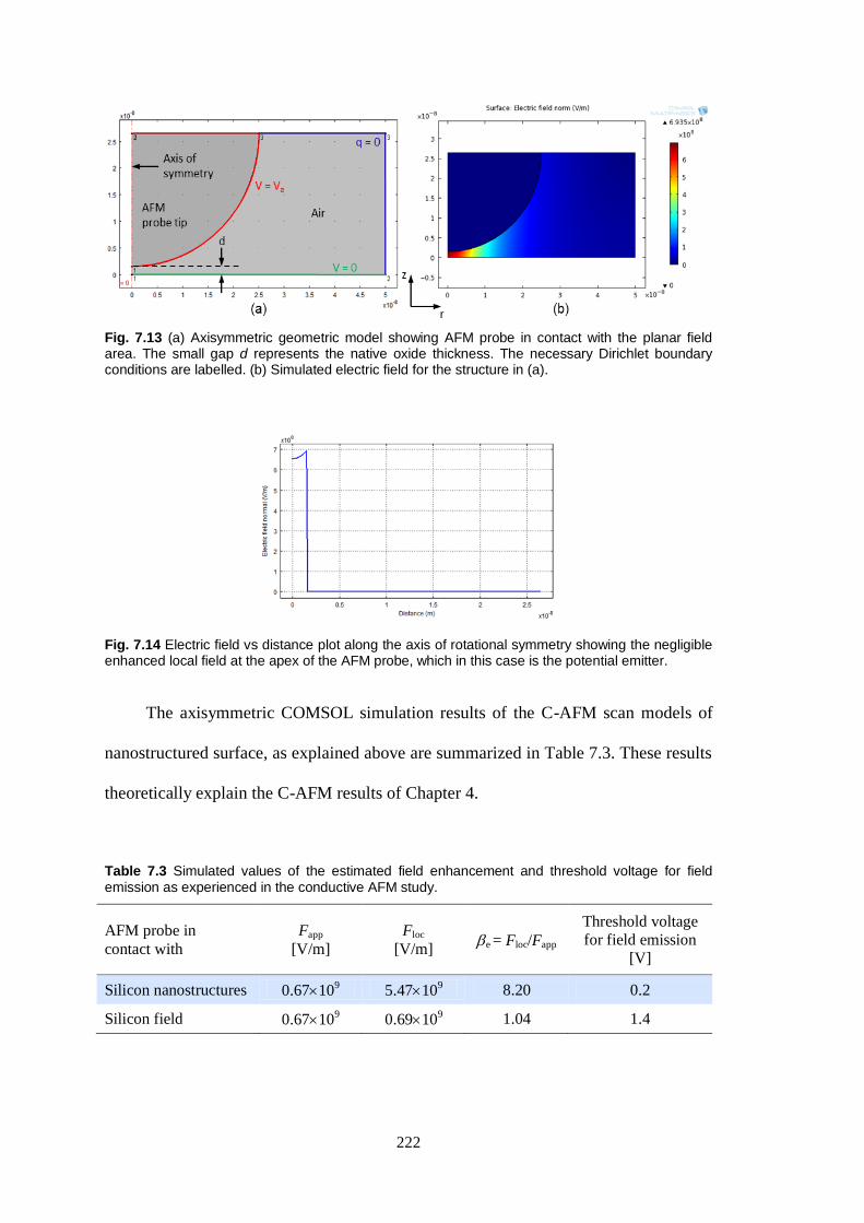
222
Fig. 7.13 (a) Axisymmetric geometric model showing AFM probe in contact with the planar field area. The small gap d represents the native oxide thickness. The necessary Dirichlet boundary conditions are labelled. (b) Simulated electric field for the structure in (a).
Fig. 7.14 Electric field vs distance plot along the axis of rotational symmetry showing the negligible enhanced local field at the apex of the AFM probe, which in this case is the potential emitter.
The axisymmetric COMSOL simulation results of the C-AFM scan models of
nanostructured surface, as explained above are summarized in Table 7.3. These results
theoretically explain the C-AFM results of Chapter 4.
Table 7.3 Simulated values of the estimated field enhancement and threshold voltage for field emission as experienced in the conductive AFM study.
AFM probe in
contact with
Fapp
[V/m]
Floc
[V/m] e = Floc/Fapp
Threshold voltage
for field emission
[V]
Silicon nanostructures 0.67109 5.4710
9 8.20 0.2
Silicon field 0.67109 0.6910
9 1.04 1.4

223
7.4 Field Enhancement in the Fabricated Devices
Self-assembled silicon nanostrucutres were used as emitting sites for the cathode of
the fabricated field emission diode (Chapter 5). A 300 nm oxide film isolated the
silicon-substrate cathode from the anode, which was made out of 90-nm thick
tungsten. The isotropic etch of the oxide during device-area or cathode (anode)
opening definition created an undercut. Together with the undercut, a planned
overetching of the oxide resulted an overhung anode around the periphery of the
opened cathode area. It was done to increase the collection of emitted electrons from
the nanostructures that would grow on the cathode surface underneath the anode and
some reasonable distance away from the projected anode edge on the cathode. The
axisymmetric simulations were performed for these structures to investigate effect of
field enhancement for small radius and height variations of the emitting tips.
Simulations were also done to optimize cathode (anode) opening radius so that
adequate number of nanostructures come under the influence of a designed local field.
Figure 7.15(a) shows the geometric setup along with the boundary conditions for
the simulation and Fig. 7.15(b) the automated mesh generated in COMSOL. The
applied field for the simulations was 3.33106 V/m. The parameters investigated were
(a) (b)
Fig. 7.15 (a) Geometric model and boundary conditions for the simulation of the fabricated field-
emission diode. (b) Automatic mesh generated for the setup by COMSOL for the simulation.

224
r, the radius of curvature of the nanostructure tip, h, the height of the nanostructure,
and ao, the cathode (anode) opening, which was also the distance at which
nanostructures were placed from the projection of opened anode edge on the cathode
for the simulation. The simulation results are discussed in the following sub-sections.
7.4.1 Tip Radius Effect
The first set of simulation results (Fig. 7.16(a)) show that the electric field depends on
the radius of the emitting tip significantly. The relation between the field enhancement
factor and the radius of the nanostructure apex in the region of interest is given
approximately by
(7.11)
The power relation in Eq. (7.11) gives a straight line when log (e) is plotted as a
function of log (r) and becomes
( ) (7.12)
and is evident with a slope of – 0.75 for the fitting line (Fig. 7.16(b)).
The enhancement factor e grows steeply with the radius r as the radius proceeds
below the silicon lattice constant 5.43 Å and enters into the atomic scale. These results
also confirm the experimental characterization results that atomic-scale tip is essential
for the range of field enhancement that is required for field emission from
nanoemitters at low voltage.
For the comparison as to the shape of the nanoemitters, simulation results of
standard rounded nanowhiskers and nanocones with similar tip radius and height are
also plotted in Fig. 7.16(a). As expected, the rounded nanowhisker, essentially vertical
nanowires with rounded end, exhibited higher field enhancement and the cones lower
than the same from the grown silicon nanoemitters. However, the variation in field

225
enhancement is observed to be within about 10% of the enhancement of the silicon
nanostructures.
Fig. 7.16 (a) Field enhancement factor e is plotted with respect to radius r of the nanostructure apex in the range of interest (blue squares) and the corresponding power relation fit (black line).
Also plotted are e for equivalent radius rounded whisker (in green) and pyramidal cone (in red) nanoemitters in a similar device environment. GNS nanostructures maintained the middle ground.
(b) log (e) versus log (r) plot (blue) has a straight line fit with the slope giving the power relation.
7.4.2 Sensitivity to Small Height Variation
Simulations were carried out for the nanostructure heights of 10 1 nm to examine
field enhancement sensitivity to small height variation. The results are plotted in

226
Fig. 7.17, which shows a linear relation of the extracted data given by the approximate
equation in the range of interest as
(7.13)
The slope of Eq. (7.13) indicates that the enhancement factor changes by 5 units
for a nanometre of height change. These changes are within 10% of the simulated
electric field enhancement at the vicinity of the grown nanostructure height.
Fig. 7.17 Variation of field enhancement factor e with respect to the nanostructure height h in the range of interest (blue circles) and the corresponding linear fit (black line).
7.4.3 Cathode-Opening Area Optimization
The third, and the last, investigation of the simulated field enhancement from the
silicon nanostructures was to find an optimized cathode-opening design radius, ao,
which is also the radius of the opened anode area for the fabricated device. The idea
here is to find ao, the maximum distance on the opened cathode surface from the
centre to a point directly under the extended open anode edge such that the
nanostructures at both ends experience field enhancement within a certain minimum
limit. The maximum resolution requirement for the lithography then is determined as
2ao for an optimized emitting cathode source.

227
Simulation results of the investigation are shown in Fig. 7.18. The curve in
Fig. 7.18 shows a maximum at ao around 100 nm. The lower field enhancements
below the maximum value are from the field screening effect from the neighbouring
oxide structure, a phenomenon which was verified with observation of no such
reduction of field enhancements in simulations without the oxide structure. The same
trend observed above the maximum value is from the increasing diagonal distance
between the nanostructure and the anode edge.
Fig. 7.18 Variation of field enhancement factor as position of a nanostructure on the cathode surface moves away from the point directly under the anode edge above.
If an 8% variation in field enhancement factor is considered among participating
nanostructures for reasonably uniform field emission from an emitting cathode source,
we find ao to be 250 nm (Fig. 7.18). An optimized field emission diode, therefore, can
be fabricated with arrays of open areas for cathode (anode) with a diameter of 500 nm
when the same process as described in Chapter 5 is used.
7.5 Conclusions
Charge conservation was considered in the mathematical modelling of an electrostatic
system space to execute the axisymmetric simulation of different physical

228
arrangements of the silicon nanostructures using COMSOL. The conductive AFM and
the device level environments were modelled for geometry and for the relevant
boundary conditions and the same were simulated to estimate electric field
enhancements from these nanostructures.
Adequate local field enhancement required for field emission was observed at
very low applied voltage at the nanostructure apex upon contact with an AFM probe.
Whereas, the estimated field enhancement from such contacts over planar silicon field
was insufficient to initiate field emission at low voltages. These results confirm the
conductive AFM experimental (Chapter 4) findings.
The simulated results from the field-emission device environment provided
approximate relationships between the electric field enhancement factor and the apex
radius and the height of the nanostructures in the range of interest. However, the
simulated field enhancement factors were somewhat lower than those found from the
calculated values from experimental data (Chapter 6) analysis. The limitation could be
due to the quantum-mechanical nature of the problem for the ultrasharp tip space,
while the simulation was concerned primarily with pure electrostatics. In any case, the
simulations provided the approximate guide and the basis for estimation of field
enhancements and the relations can be incorporated into a quantum-mechanical
treatment of field emission.
The results obtained from the simulation in regard to cathode-opening radius can
be used to improve the field emission diode design. An optimized cathode area
eventually minimizes the device size by eliminating areas with nanostructures not
contributing in field-emission inside the operating voltage regime of the device.
229
Chapter 8
CONCLUSIONS AND FUTURE WORK
Vacuum nanoelectronics based on field emission from conventional and exotic
nanoemitters have enticed much attention in recent years. In this thesis self-assembled
silicon nanostructures grown in a single electron beam annealing step were studied as
a potential source of field emission for vacuum nanoelectronics. Integrated field
emission devices were, in the process, fabricated using those self-assembled silicon
nanostructures and were characterized. Field enhancement was modelled and
simulations were carried out to extend our understanding of the physics of field
emission from silicon and to advance the technology.
In the remainder of this final chapter the experimental and simulation results
embodied in this thesis are summarised. The author’s suggestions for related future
work on the subject are also presented.
8.1 Summary of Results
We have extensively studied the electrical transport characteristics of self-assembled
silicon nanostructures by using conductive atomic force microscopy (C-AFM). A

230
simple and lithography-free fabrication technique was used to grow whiskerlike
protruding silicon nanostructures on untreated n- and p-type silicon surfaces using
electron-beam annealing under high vacuum. These nanostructures self-assemble as a
result of the thermal decomposition of the native oxide, which results in atomic-scale
disorder on the silicon surface, followed by adatom diffusion, nucleation, and growth
at kinetically favorable sites. In addition to providing the energy source for sample
heating, the electron beam is essential in this process to promote surface diffusion of
adatoms through inelastic energy transfer events.
Our C-AFM investigations of these grown nanostructures showed higher
electrical conductivities in the nanostructured silicon surface compared to the
conductivities in the surrounding planar silicon substrate region. We reported non-
ideal diodic behaviour with high ideality factors for the individual nanostructure- AFM
tip Schottky nanocontacts, demonstrative of the presence of a significant field
emission component in the analysed current transport phenomena. The practical
demonstration of field emission was recorded in the lift-mode interleave C-AFM scans
which conspicuously showed decaying of corresponding currents from areas
immediately above the nanostructures as the AFM tip was moved away from the
nanostructured surface.
We have reported successful fabrication of field emission diodes using the self-
assembled silicon nanostructures integrated in a CMOS process flow. These self-
assembled silicon nanostructures represented the electron-emitting nanoprotrusions of
an otherwise planar silicon cathode. The fabricated devices had a turn-on voltage as
low as ~ 0.6 V. The low turn-on voltage offered practical demonstration that these
devices can be integrated into the standard CMOS technology.

231
The self-assembly and growth of n-type silicon nanostructures of height
~10 nm occurred at the last step of the process, i.e., in the electron beam annealing
step. The process consisted of three major photolithographic definition steps followed
by three etching steps to define contacts to substrate, metals, and cathode opening
areas. After the contact definition, ions were implanted to contact areas to make the
contacts ohmic. The fabricated devices were by no means optimized for cathode open
array area or nanostructures height or for device performance; they are essentially a
practical demonstration of proof of the concept, the concept being that the self-
assembled silicon nanostructures can be used to fabricate field emission devices that
can be integrated in a CMOS technology. The demonstration has been a conclusive
contribution to the silicon nanostructure device effort undertaken jointly by the
department and GNS Science.
In any case, the fabricated devices exhibited reproducible I-V characteristics
and these characteristics were further studied to extract field emission parameters
using a unified approach in the transition region of the device operation. Independent
equations from the Schottky emission and Fowler-Nordheim emission regimes were
extended into the transition region and solved simultaneously to get the required
barrier height, field conversion factor, and total emitting area. The extraction method
developed was consistent and provided reliable information about the on-set of field
emission in these devices, which can be used effectively to the understanding of
electron transport mechanisms in the transition regime between the Schottky and
Fowler-Nordheim emissions.
The extracted results suggested atomically sharp nanostructure apexes, a
suggestion which was later verified in relevant field simulations. The device I-V
characteristics also confirmed the existence of an electron-supply limited saturation
232
region at high electric field. The current saturation effect can be used to an advantage
in circuit applications as a current-limiting series resistor may not be required with the
device.
Both the C-AFM and the device characterization studies were modelled and
simulated using commercial COMSOL Multiphysics software package. Results from
these finite element analyses helped to further explain the experimental results – the
field developed at various operating environments. The nanostructure tip radius effect
and sensitivity to small nanostructure height variation were investigated and
mathematical relations were established for the nanostructure regime of our interest.
The cathode-opening area optimization technique was also demonstrated.
Through this experimental research, modelling and simulation, a primary
understanding of the different electrical characteristics of an individual silicon
nanostructure, its contact behaviour with a metallic tip and its role in a device
environment have been made possible. The research provided a means to integrate
field emission devices in CMOS technology. The main objectives enumerated in
Chapter 1 for the research have indeed been successfully fulfilled.
8.2 Recommendations for Future Work
From the experience and understanding gained through the investigative work on the
self-assembled nanostructures and from the physical fabrication and characterization
of the field emission diodes, supported by the modelling and simulation of the field
enhancement phenomenon the author envisages the future direction of the research in
the related field continuing with the same material. These envisioned future works are

233
suggested under three different themes below to further the outcome of this present
research.
8.2.1 Further investigation of individual silicon nanostructures
The reported conductive AFM work was carried out under standard atmospheric
condition and therefore contained associated distortion from the various adsorbed
materials on the emitter surface. Native oxide that formed instantaneously when
silicon was exposed to air also influenced the field emission properties of these
nanostructures. In order to measure more accurate values for field emission
characterization these studies are suggested to be carried out in an ultra-high vacuum
environment. The service of the Scanning Tunnelling Microscope (STM), capable of
performing conductive AFM spectroscopy in ultra-high vacuum (UHV) and which has
recently become available in the university’s Department of Physics, can be taken for
the purpose. Preliminary UHV-STM measurements have been performed (Fig. 8.1);
however, these studies were interrupted by the Christchurch earthquakes.
(a) (b)
Fig. 8.1 (a) An STM scan of nanostructured surface with gap voltage, Vg = 2 V, and current feedback set at Is = 2 pA. (b) Profile across the drawn (green) line in (a).

234
8.2.2 Fabrication of optimized field emission diodes
As mentioned earlier, the fabricated devices were neither optimized for cathode open
array areas nor for nanostructure heights. These quantities can be optimized for a
particular application or power requirement. Similarly, the thickness of the oxide
between the electrodes can be optimized based on power source, hence field,
requirements of the application and usage of the device, allowing for adequate
leverage from oxide breakdown. A vacuum seal may be required to ensure ballistic
electron transport, if thicker oxides are used.
The finite element method (FEM) simulation in COMSOL (demonstrated in
Chapter 7) can be used to approximate these quantities as the starting step for
optimization. For example, for 10 nm nanostructures with 300 nm thick field oxide,
the optimized cathode opening area would be circles of a radius of 250 nm as found in
Section 7.4.3. Again these circular open holes can be arranged in different array
configurations to make the maximum area utilization of a given designed total cathode
area (e.g., hexagonal array). Likewise, the pitch of the array can be optimized to the
lithographic resolution limit of a process and with oxide overetch the entire anode
plate can be freed above the cathode (Fig. 3.11(b)); an arrangement which would
increase the emission current density tremendously. As an advanced development, the
device open area over anode plate can be closed and therefore sealed in vacuum with
rotating steep glancing-angle deposition (Fig. 2.13) of metal. A redefinition of the
metals for anode plate and cathode contact connections would be required in this case.
To reduce leakage current and to increase rectification ratio, the individual
devices can be isolated through introduction of wells in the substrate and shallow
oxide trenches surrounding the devices as in a standard CMOS process. A high energy
ion implanter may be required for the implementation of wells in the design.
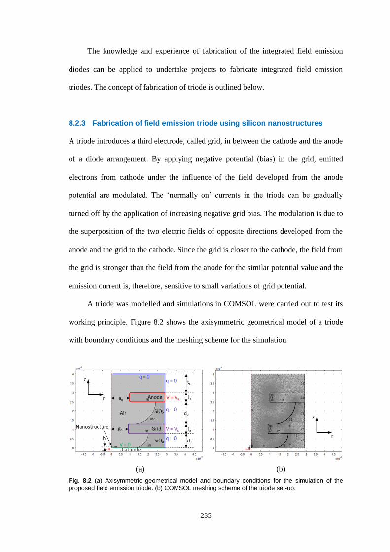
235
The knowledge and experience of fabrication of the integrated field emission
diodes can be applied to undertake projects to fabricate integrated field emission
triodes. The concept of fabrication of triode is outlined below.
8.2.3 Fabrication of field emission triode using silicon nanostructures
A triode introduces a third electrode, called grid, in between the cathode and the anode
of a diode arrangement. By applying negative potential (bias) in the grid, emitted
electrons from cathode under the influence of the field developed from the anode
potential are modulated. The ‘normally on’ currents in the triode can be gradually
turned off by the application of increasing negative grid bias. The modulation is due to
the superposition of the two electric fields of opposite directions developed from the
anode and the grid to the cathode. Since the grid is closer to the cathode, the field from
the grid is stronger than the field from the anode for the similar potential value and the
emission current is, therefore, sensitive to small variations of grid potential.
A triode was modelled and simulations in COMSOL were carried out to test its
working principle. Figure 8.2 shows the axisymmetric geometrical model of a triode
with boundary conditions and the meshing scheme for the simulation.
(a) (b)
Fig. 8.2 (a) Axisymmetric geometrical model and boundary conditions for the simulation of the proposed field emission triode. (b) COMSOL meshing scheme of the triode set-up.

236
The optimization parameters for a triode structure are, but not limited to,
distance between the grid and the cathode d1, grid thickness tg, distance between the
grid and the anode d2, grid opening go and anode opening ao, and the nanostructure
height h (Fig. 8.2(a)). All of these parameters affect the field enhancement at the
nanostructure apex. The FEM simulation results for potential and field distributions in
the triode are shown in Fig. 8.3.
Fig. 8.3 Simulated potential and field distributions with h = 20 nm: (a) Va = 10 V, Vg = 0 V, (b) Va = 10 V, Vg = -0.1 V, and (c) Va = 10 V, Vg = -0.3 V. Small variation in grid potential caused large change in resultant field.

237
The grid modulation of resultant electric field can be clearly observed in
Fig. 8.3. The field at an anode potential of 10 V with no grid bias was 5.4108 V/m.
The field was decreased to 4.3108 V/m with grid bias of -0.1 V and further decreased
to 2.2108 V/m when the grid bias was set to -0.3 V. The simulated field values at the
nanostructure apex were plotted as a function of anode voltage for different grid biases
in Fig. 8.4. Because of the existence of the grid electrode, the field enhancement from
the anode applied field was not in the range of that in the diode case, even when there
was no bias. Therefore, nanostructures with larger heights would be required for a
field emission triode. Fortunately, nanostructure heights are controlled through the
electron beam annealing parameters and growth of nanostructures over 20 nm high
was reported with the growth showing a linear dependence on anneal time [57].
Fig. 8.4 Simulated electric field at the nanostructure apex vs. anode voltage curves for different grid voltages. Field is reduced with the increase of negative grid bias at a particular anode voltage.
In the integration of the proposed triode in the CMOS technology, similar
fabrication process steps as in the diode fabrication can be taken. Figure 8.5 outlines
the major process steps, which include five photolithographic pattern transfer
steps involving five photomasks, namely, cathode contact, metal 1, metal 1 contact,
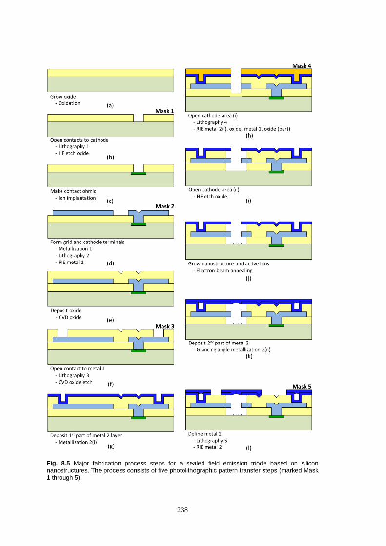
238
Fig. 8.5 Major fabrication process steps for a sealed field emission triode based on silicon nanostructures. The process consists of five photolithographic pattern transfer steps (marked Mask 1 through 5).
239
cathode-opening area, and metal 2 masks. Figure 8.5 is self-explanatory and the
process is not detailed here for brevity. The success of the fabrication of triode lies
with precision alignment of these five level mask patterns, the quality of deposited
oxide film (Fig. 8.5(e)), the anisotropic etch for cathode opening area (Fig. 8.5(h)), and
if vacuum sealed, the steep glancing-angle stage two of metal 2 deposition
(Fig. 8.5(k)). If a vacuum seal is not used, mask 5 must be exposed before mask 4 and
the steps can be rearranged accordingly.
8.3 Final Comments
The focus of this thesis has been on the primary understanding of the field emission
phenomenon from the self-assembled silicon nanostructures and on the initial
development of the prototype integrated field emission diodes using those
nanostructures. The optimization of the diode, using the method mentioned in
Section 8.2.2, would be an important addition to the research geared towards its
acceptance in industrial application.
Finally, the author looks forward to the day when high-end professional audio
power amplifiers, microphone preamplifiers, and other applications that use ‘old’
bulky vacuum triodes would be replaced by the tiny integrated silicon field emission
triodes as contemplated in Section 8.2.3. The work presented in this thesis, the author
hopes, would contribute to that forthcoming vacuum nanoelectronic revolution.

240

241
Appendix A
Selected Fundamental Physical Constants
Physical constant Symbol Value Unit
Angstrom unit Å 10-10
m
Boltzmann constant k 1.38110-23
JK-1
Elementary charge q 1.60210-19
C
Electron rest mass m0 9.10910-30
kg
Electron volt eV 1.60210-19
J
Permittivity in vacuum 8.85410-14
Fcm-1
Planck constant h 6.62610-34
Js
Reduced Planck Constant 1.05510-34
Js
Speed of light in vacuum c 2.998108 ms
-1
Standard atmosphere 1.013105 Nm
-2
Thermal voltage at 300 K kT/q 0.0259 V
Reference:
All values quoted above are taken from S. M. Sze, Physics of Semiconductor Devices, New
York: John Willey & Sons, p. 847, 1981.

242
Appendix B
Electron Work Function of Selected Elements
Element Symbol Plane Work Function
eV Method
Aluminium Al 100 4.20 PE
110 4.06 PE
111 4.26 PE
Carbon C polycr ~ 5.00 CPD
Calcium Ca polycr 2.87 PE
Caesium Cs polycr 1.95 PE
Copper Cu 100 5.10 FE
110 4.48 PE
111 4.94 PE
Iron Fe 100 4.67 PE
111 4.81 PE
Hafnium Hf polycr 3.90 PE
Molybdenum Mo 100 4.53 PE
110 4.95 PE
111 4.55 PE
Sodium Na polycr 2.36 PE
Neodymium Nd polycr 3.20 PE
Nickel Ni 100 5.22 PE
110 5.04 PE
111 5.35 PE
Palladium Pd polycr 5.22 PE
111 5.60 PE
Selenium Se polycr 5.90 PE
Silicon Si n 4.85 CPD
p 100 ~ 4.91 CPD
p 111 4.60 PE
Tungsten W polycr 4.55 CPD
100 4.63 FE
110 5.22 FE
111 4.45 FE
PE – Photoelectric effect; FE – Field emission; CPD – Contact potential difference; polycr – polycrystalline sample.
Reference:
CRC Handbook of Chemistry and Physics, CRC Press, p. 12-124, 2012.

243
Appendix C
Properties of Silicon
Physical property Symbol Value Unit
Atomic density Na 5.01022
cm-3
Atomic weight Ar 28.09
Crystal structure Diamond
Density d 2.328 gcm-3
Dielectric constant 11.9
Effective density of states in conduction band Nc 2.81019
cm-3
Effective density of states in valence band Nv 1.041019
cm-3
Effective mass m*/m0
Electrons m*l , m*t 0.98, 0.19
Holes m*lh , m*th 0.16, 0.49
Electron affinity 4.05 eV
Energy gap at 300 K Eg 1.12 eV
Intrinsic carrier concentration ni 1.01010
[1] cm-3
Intrinsic Debye length D 24 m
Intrinsic resistivity i 2.3105 cm
Lattice constant a 5.43 Å
Linear coefficient of thermal expansion L/LT 2.610-6
°C-1
Melting point 1415 °C
Minority carrier lifetime 2.510-3
s
Mobility (drift) [electron, hole] e , h 1500, 450 cm2V
-1s
-1
Optical phonon energy Eopt 0.063 eV
Phonon mean free path [electron, hole] o 76, 55 Å
Specific heat Cs 0.7 Jg-1°C
-1
Thermal conductivity at 300 K 1.5 Wg-1°C
-1
Thermal diffusivity ath 0.9 cm2s
-1
Vapour pressure [at 1650 °C, 900 °C] 1, 10-6
Pa
References:
All values quoted above are taken from S. M. Sze, Physics of Semiconductor Devices, New
York: John Willey & Sons, pp. 850-851, 1981 except [1] A. B. Sproul and M. A. Green,
“Improved value for the silicon intrinsic carrier concentration from 275 to 375 K,” Journal of
Applied Physics, 70 (2), pp. 846-854, 1991.

244
Appendix D
Properties of SiO2
Physical property Symbol Value Unit
Structure Amorphous
Density d 2.2 gcm-3
Dielectric constant 3.9
Dielectric strength ~ 107 Vcm
-1
Energy gap at 300 K Eg 9 eV
Infrared absorption band 9.3 m
DC resistivity at 25°C 1014
-1016
cm
Coefficient of thermal expansion L/LT 510-7
°C-1
Melting point ~ 1600 °C
Refractive index n 1.46
Thermal conductivity at 300 K 0.014 Wg-1°C
-1
Reference:
All values quoted above are taken from S. M. Sze, Physics of Semiconductor Devices, New
York: John Willey & Sons, p. 852, 1981.
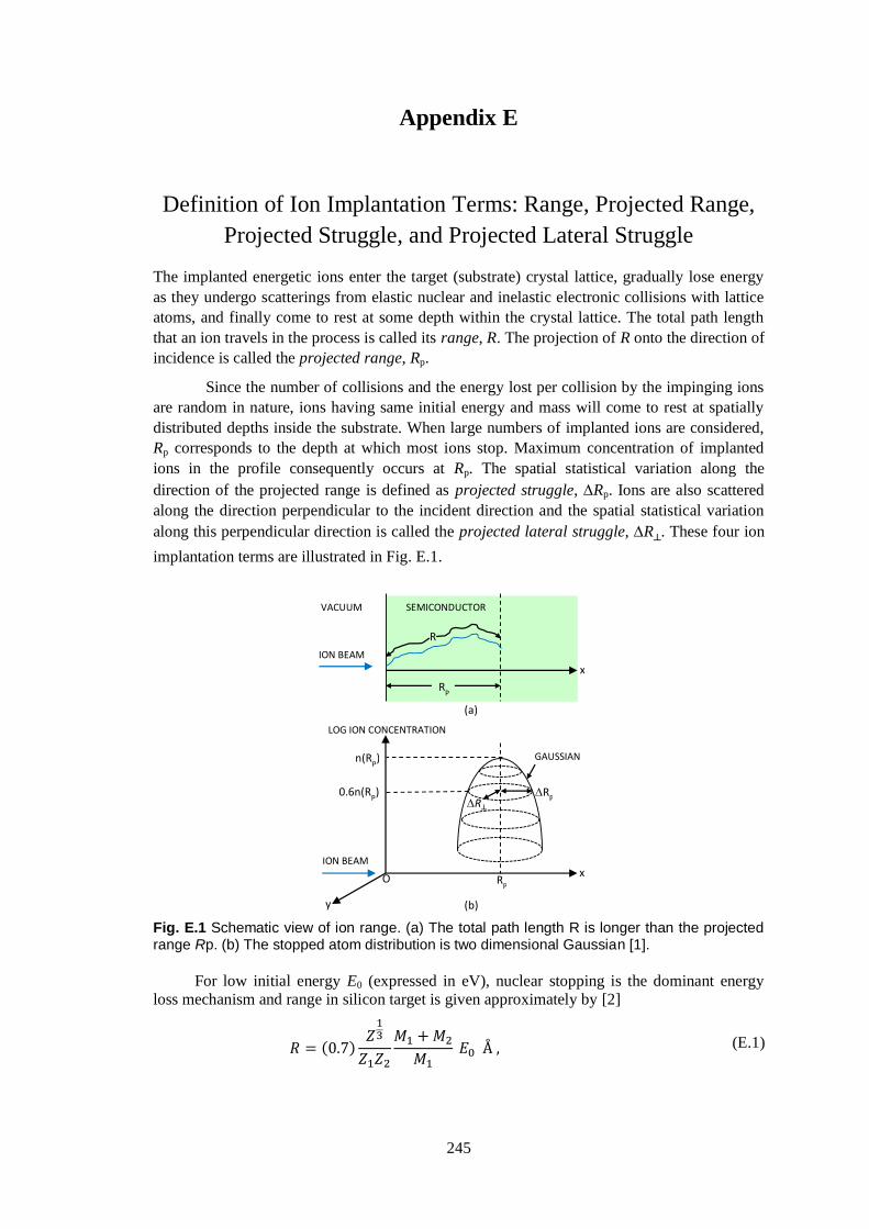
245
Appendix E
Definition of Ion Implantation Terms: Range, Projected Range,
Projected Struggle, and Projected Lateral Struggle
The implanted energetic ions enter the target (substrate) crystal lattice, gradually lose energy
as they undergo scatterings from elastic nuclear and inelastic electronic collisions with lattice
atoms, and finally come to rest at some depth within the crystal lattice. The total path length
that an ion travels in the process is called its range, R. The projection of R onto the direction of
incidence is called the projected range, Rp.
Since the number of collisions and the energy lost per collision by the impinging ions
are random in nature, ions having same initial energy and mass will come to rest at spatially
distributed depths inside the substrate. When large numbers of implanted ions are considered,
Rp corresponds to the depth at which most ions stop. Maximum concentration of implanted
ions in the profile consequently occurs at Rp. The spatial statistical variation along the
direction of the projected range is defined as projected struggle, Rp. Ions are also scattered
along the direction perpendicular to the incident direction and the spatial statistical variation
along this perpendicular direction is called the projected lateral struggle, R┴. These four ion
implantation terms are illustrated in Fig. E.1.
Fig. E.1 Schematic view of ion range. (a) The total path length R is longer than the projected range Rp. (b) The stopped atom distribution is two dimensional Gaussian [1].
For low initial energy E0 (expressed in eV), nuclear stopping is the dominant energy
loss mechanism and range in silicon target is given approximately by [2]
( )
(E.1)
VACUUM SEMICONDUCTOR
ION BEAM x
LOG ION CONCENTRATION
GAUSSIAN
ION BEAM
(a)
x
y
O
RP
RP
R
RP
R┴
n(RP)
0.6n(RP)
(b)
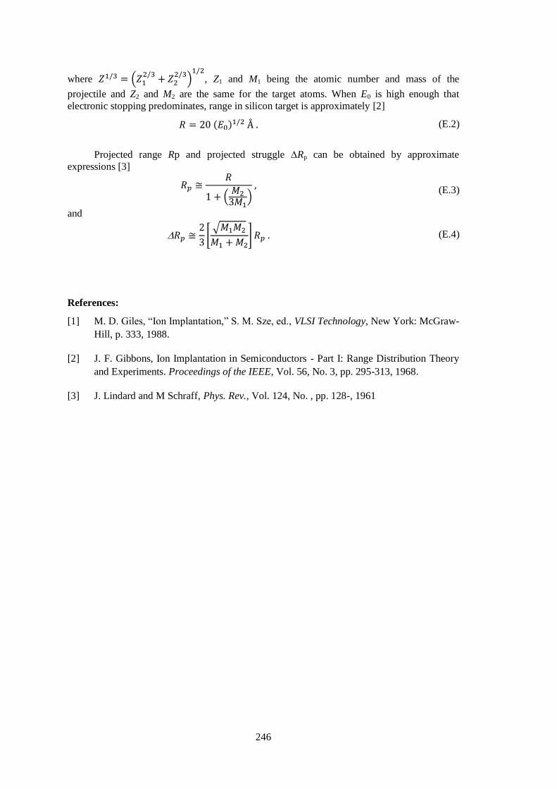
246
where (
)
, Z1 and M1 being the atomic number and mass of the
projectile and Z2 and M2 are the same for the target atoms. When E0 is high enough that
electronic stopping predominates, range in silicon target is approximately [2]
( ) (E.2)
Projected range Rp and projected struggle Rp can be obtained by approximate
expressions [3]
(
)
(E.3)
and
[√
] (E.4)
References:
[1] M. D. Giles, “Ion Implantation,” S. M. Sze, ed., VLSI Technology, New York: McGraw-
Hill, p. 333, 1988.
[2] J. F. Gibbons, Ion Implantation in Semiconductors - Part I: Range Distribution Theory
and Experiments. Proceedings of the IEEE, Vol. 56, No. 3, pp. 295-313, 1968.
[3] J. Lindard and M Schraff, Phys. Rev., Vol. 124, No. , pp. 128-, 1961

247
References
[1] Ivor Brodie addressed those present in the First International Vacuum
Microelectron--ics Conference in June 1988 as fellow ‘Microelectronikers’. I.
Brodie, “Pathways to Vacuum Microelectronics,” IEEE Transactions on
Electron Devices, Vol. 36, No. 11, pp. 2637-2640, 1989.
[2] H. H. Busta, “Vacuum Microelectronics – 1992,” Journal of Micromechanics
and Microengineering, Vol. 2, pp. 43-74, 1992.
[3] I. Brodie and P. R. Schwoebel, “Vacuum Microelectronic Devices,”
Proceedings of the IEEE, Vol. 82, No. 7, pp. 1006-10034, 1994.
[4] H. F. Gray, “Vacuum Microelectronics 1996: Where We Are and Where We
are Going,” 9th International Vacuum Microelectronics Conference, St.
Petersburg, pp. 1-3, 1996.
[5] B. R. Chalamala, R. R. Heuss, and B. E. Gnade, “Displaying a Bright Future,”
Circuits and Devices, pp. 19-30, 2000.
[6] J. A. Fleming, “Instrument for converting alternating electric currents into
continuous currents,” US Patent No. 803684, 1905.
[7] L. De Forest, “Space telegraphy,” US Patent No. 879532, 1908.
[8] S. Okamura, Ed., History of Electron Tubes, Ohmsha Ltd., Tokyo, 1994.
[9] J. Bardeen and W. H. Brattain, “The Transistor, A Semiconductor Triode,”
Physical Review, vol. 74, no. 2, pp. 230–231, 1948.
[10] R. Feynman, “There is plenty of room at the bottom,” Journal of
Microelectromechanical Systems, Vol. 1, No. 1, 1992 (Reprint).
[11] K. R. Shoulders, “Microelectronics using electron beam activated machining
techniques,” Advances in Computers, Franz L. Alt, Ed., Vol. 2, pp. 135-293,
1961.
[12] C. A. Spindt, “A Thin-Film Field-Emission Cathode,” Journal of Applied
Physics, Vol. 39, pp. 3504-3505, 1968.
[13] R. N. Thomas and H. C. Nathanson, “Photosensitive field emission from Si
point arrays,” Applied Physics Letter, Vol. 21, pp. 384-386, 1972.

248
[14] R. N. Thomas and H. C. Nathanson, “Transmissive-mode silicon field emission
array photoemitter,” Applied Physics Letter, Vol. 21, pp. 387-389, 1972.
[15] D. Schroder, R. N. Thomas, J. Vine, and H. C. Nathanson, “The
Semiconductor Field-Emission Photocathode,” IEEE Transactions on Electron
Devices, Vol. 21, No. 12, pp. 785-798, 1974.
[16] G. Bennig, H. Rohrer, Ch. Gerber, and E. Weibel, “Surface Studies by
Scanning Tunneling Microscopy,” Physical Review Letters, Vol. 49, No. 1, pp.
57-60, 1982.
[17] R. F. Greene, H. F. Gray, and G. J. Campisi, “Vacuum Integrated Circuits,”
IEDM Technical Digest, p. 172, 1985.
[18] H. F. Gray, G. J. Campisi, and R. F. Greene, “A Vacuum Field Effect
Transistor Using Silicon Field Emitter Arrays,” IEDM Technical Digest, pp.
776-779, 1986.
[19] H. F. Gray, “The Physics of Vacuum Microelectronic Devices,” IEEE
Transaction on Electron Devices, Vol. 36, No. 11, p. 2599, 1989 (Abstract).
[20] C. A. Spindt, C. E. Holland, A. Rosengreen, and I. Brodie, “Field-Emitter
Arrays for Vacuum Microelectronics,” IEEE Transaction on Electron Devices,
Vol. 38, No. 10, pp. 2355-2363, 1991.
[21] T. Utsumi, “Vacuum Microelectronics: What’s New and Exciting”, IEE
Transaction on Electron Devices, Vol. 38, No. 10, pp. 2276-2283, 1991.
[22] G. Bennig, C. F. Quate, and C. Gerber, “Atomic force microscope,” Physical
Review Letter, Vol. 56, No. 9, pp. 930-933, 1986.
[23] S. O. Kasap, Principles of Electronic Materials and Devices, McGraw Hill,
New York, p. 197, 2006.
[24] S. O. Kasap, Principles of Electronic Materials and Devices, McGraw Hill,
New York, p. 294, 2006.
[25] J. Singleton, Band Theory and Electronic Properties of Solids, Oxford
University Press, London, p. 8, 2001.
[26] S. O. Kasap, Principles of Electronic Materials and Devices, McGraw Hill,
New York, p. 306, 2006.
[27] F. Reif, Fundamentals of Statistical and Thermal Physics, McGraw Hill, New
York, p. 341, 1965.

249
[28] S. Dushman, “Electron emission from metals as a function of temperature,”
Physical Review, Vol. 21, pp. 623-636, 1923.
[29] L. W. Nordheim,”The Effect of the Image Force on the Emission and
Reflexion of Electrons by Metals,” Proceedings of the Royal Society of
London. Series A, Containing Papers of a Mathematical and Physical
Character, Vol. 121, No. 788, pp. 626-639, 1928.
[30] L. M. Fisher, “A come back for the vacuum tube,” The New York Times, 18
May 1988.
[31] B. R. Chalamala, Y. Wei, and B. E. Gnade, “FED up with fat tubes,” IEEE
Spectrum, pp 44-51, April 1988.
[32] I. Brodie, “Physical considerations in vacuum microelectronic devices,” IEEE
Transactions on Electron Devices, Vol. 36, No. 11, pp. 2641-2644, 1989.
[33] A. K. Ganguly, P. M. Phillips, and H. F. Gray, “Linear theory of a field‐
emitter‐array distributed amplifier,” Journal of Applied Physics, Vol. 67, No.
11, pp. 7098-7110, 1990.
[34] H. H. Busta, J. E. Pogemiller, and B. J. Zimmerman, “The field emitter triode
as a displacement/pressure sensor,” Journal of Micromechanics and
Microengineering, Vol. 3, pp. 49-56, 1993.
[35] X. Shanhong, T. Xinxin, S. Jie, and C. Shaofeng, “Novel “cathode-on-
membrane” VME pressure sensor,” Journal of Electronics, Vol. 18, No. 3, pp.
255-259, 2001.
[36] T. E. Felter, “Vacuum microelectronics and the mass spectrometer,” 25th IEEE
International Conference on Plasma Science, Raleigh, North Carolina, USA,
June 1-4, IEEE Conference Record – Abstracts, p. 126, 1998.
[37] J. B. Cho, H. J. Yoon, S. S. Yang, K. H. Koh and S. Lee, “Fabrication and
operation of triode electron emitters as ion source for miniature mass
spectrometer,” IEEE 20th International Vacuum Nanoelectronics Conference
(IVNC), Chicago, Illinois, USA, July 8-12, Technical Digest, pp. 4-5, 2007.
[38] K. Sawada, M. Tabe, Y. Ishikawa, and M. Ishida, “Field electron emission
device using silicon nanoprotrusions,” Journal of Vacuum Science &
Technology B, Vol. 20, No. 3, pp. 787 (4 pages), 2002.
[39] D. A. Carder and A. Markwitz, “Field emission measured from nanostructured
germanium and silicon thin films,” Applied Surface Science, Vol. 256, No. 4,
pp. 1003-1005, 2009.
250
[40] Hua Qin, Renbing Tan, Jonghoo Park, Hyun-Seok Kim, and Robert H. Blick,
“Direct observation of sub-threshold field emission from silicon
nanomembranes,” Journal of Applied Physics, Vol. 109, 124504 (5 pages),
2011.
[41] H. X. Wang, N. Jiang, H. Hiraki, Y. Harada, H. Zhang, J. Wang, M. Haba, and
A. Hiraki, “Fabrication of field-emission cathode ray tube with a unique
nanostructure carbon electron emitter”, Journal of Vacuum Science &
Technology B, 26, No. 2, pp. 698 (4 pages), 2008.
[42] B. C. Smith, C. E. Hunt, I. Brodie, and A. C. Carpenter , “High-performance
field-emission electron gun using a reticulated vitreous carbon cathode”,
Journal of Vacuum Science & Technology B, Vol. 29, No. 2, pp. 02B108 (5
pages), 2011.
[43] W. Zhu, C. Bower, G.P. Kochanski, and S. Jin, “Electron field emission from
nanostructured diamond and carbon nanotubes”, Solid-State Electronics, Vol.
45, No. 6, pp. 921-928, 2001.
[44] S. A. Gavrilov, É. A. Il’ichev, É. A. Poltoratskiĭ, G. S. Rychkov, V. V.
Dvorkin, N. N. Dzbanovsky, and N. V. Suetin, “Carbon Nanotube Field
Emitters for Planar Emission Vacuum Micro- and Nanoelectronics”, Technical
Physics Letters, Vol. 30, No. 7, pp. 609–611, 2004.
[45] O. Yilmazoglu, R. Joshi, A. Popp, D. Pavlidis, and J. J. Schneider,
“Pronounced field emission from vertically aligned carbon nanotube blocks
and bundles,” Journal of Vacuum Science & Technology B, Vol. 29, No. 2,
02B106 (5 pages), 2011.
[46] S. A. Lyashenko, A. P. Volkov, R. R. Ismagilov, and A. N. Obraztsov, “Field
electron emission from nanodiamond”, Technical Physics Letters, Vol. 35, No.
3, pp. 249–252, 2009.
[47] N. Ghosh, W. P. Kang, J. L. Davidson, “Nanodiamond lateral field emission
vacuum logic or gate,” Electronics Letters, Vol. 47, No. 16, pp. 926-927, 2011.
[48] L. Liao, J.C. Li, D.F. Wang, C. Liu, and Q. Fu, “Electron field emission studies
on ZnO nanowires”, Materials Letters, Vol. 59, No. 19-20, pp. 2465-2467,
2005.
[49] K. S. Yeong and J. T. L. Thong, “Field emission properties of individual zinc
oxide nanowire field emitter,” Journal of Vacuum Science & Technology B,
Vol. 26„ No.3, pp. 983-989, 2008.

251
[50] A. Evtukh, O. Yilmazoglu, V. Litovchenko, M. Semenenko, T. Gorbanyuk, A.
Grygoriev, H. Hartnagel, and D. Pavlidis, “Electron field emission from
nanostructured surfaces of GaN and AlGaN” Physica Status Solidi C, Vol. 5,
No. 2, pp. 425-430, 2008.
[51] V. Litovchenko, A. Grygoriev, A. Evtukh, O. Yilmazoglu, H. L. Hartnagel, and
D. Pavlidis, “Electron field emission from wide bandgap semiconductors under
intervalley carrier redistribution”, Journal of Applied Physics, Vol. 106,
104511 (7 pages) , 2009.
[52] M. Eyckeler, W. Mönch, T.U. Kampen, R. Dimitrov, O. Ambacher, M.
Stutzmann, “Negative electron affinity of cesiated p-GaN(0001) surfaces ,”
Journal of Vacuum Science & Technology B, Vol. 16, No. 4. pp. 2224-2228,
1998.
[53] C. I. Wu and A. Kahn, “Negative electron affinity and electron emission at
cesiated GaN and AlN surfaces,” Applied Surface Science, Vol. 162-163, pp.
250-255, 2000.
[54] Z. Liu, Y. Sun, P. Pianetta, R. F. W. Pease, “Narrow cone emission from
negative electron affinity photocathodes,” Journal of Vacuum Science &
Technology B, Vol. 23, No. 6, pp. 2758 – 2762, 2005.
[55] T. Yamada, C. E. Nebel, and T. Taniguchi, “Field electron emission properties
of n-type (111)-oriented single crystal cubic boron nitride,” Journal of Vacuum
Science & Technology B, Vol. 29, No. 2, 02B115 (5 pages), 2011.
[56] K. L. Jensen, “Theory of Field Emission,” Vacuum Microelectronics, Ed. W.
Zhu, John Wiley & Sons, pp. 33-104, 2001.
[57] S. Johnson, A. Markwitz, M. Rudolphi and H. Baumann, “Nanostructuring of
silicon (100) using electron beam rapid thermal annealing,” Journal of Applied
Physics, Vol. 96, No. 1, pp. 605-609, 2004.
[58] R. Gomer, Field Emission and Field Ionization, pp. 1-31, American Institute of
Physics, New York, 1993.
[59] CRC Handbook of Chemistry and Physics, p. 12-124, 2012.
[60] G. Fursey, Field Emission in Vacuum Microelectronics, p. xi, Kluwer
Academic, New York, 2005.
[61] L. Solymar and D. Walsh, Electrical Properties of Materials, p. 89, Oxford
University Press, 2004.

252
[62] A. G. J. van Oostrom, “Validity of the Fowler-Nordheim Model for Field
Electron Emission,” Philips Research Reports – Supplements, Vol. 21, No. 1,
pp. 1-102, 1966.
[63] C. Durkan, Current at the Nanoscale: An Introduction to Nanoelectronics, pp.
61-64, Imperial College Press, London, 2007.
[64] A. T. Fromhold, Jr., Quantum Mechanics for Applied Physics and Engineering,
pp. 237-246, Academic Press, New York, 1981.
[65] G. N. Fursey, Field Emission in Vacuum Microelectronics. pp. 1-17, Kluwer
Academic, New York, 2005.
[66] R. E. Burgess, H. Kroemer, and J. M. Houston, “Corrected values of Fowler-
Nordheim field emission function ( ) and ( ), Physical Review, Vol. 90,
No. 1, p. 515, 1953.
[67] R. H. Fowler and L. Nordheim. “Electron emission in intense electric fields,”
Proceedings of the Royal Society of London, Series A, Containing Papers of
Mathematical and Physical Character, Vol. 119, No. 781, pp. 173-181, 1928.
[68] C. Durkan, Current at the Nanoscale: An Introduction to Nanoelectronics, pp.
85-88, Imperial College Press, London, 2007.
[69] N. A. de Bruyne, “The action of strong electric fields on the current from a
thermionic cathode,” Proceedings of the Royal Society of London, Series A,
Containing Papers of a Mathematical and Physical Character, Vol. 120, pp.
423-437, 1928.
[70] S. G. Christov, “General theory of electron emission from metals,” Physica
Status Solidi, Vol. 17, No. 1, p. 11-26, 1966.
[71] L. W. Swanson and G. A. Schwind, “Review of ZrO/W Schottky cathode,” in
Handbook of Charged Particle Optics, Ed., J. Orloff, p. 1-28, 2009.
[72] L. W. Swanson and A. E. Bell, “Recent advances in field electron microscopy
of metals,” Advances in Electronics and Electron Physics, Ed., L. Marton, Vol.
32, pp. 193-309, 1973.
[73] R. Stratton, “Field emission from semiconductors,” Proc. Phys. Soc. London,
Vol. B68, pp. 746-757, 1955.
[74] R. Stratton, “Theory of field emission from semiconductors,” Physical Review,
Vol. 125, No. 1, pp. 67-82, 1962.

253
[75] F. G. Allen, “Emissivity at 0.65 micron of silicon and germanium at high
temperatures,” Journal of Applied Physics, Vol. 28, pp. 1510-1511, 1957.
[76] L. A. D’Asaro, “Field emission from silicon,” Journal of Applied Physics, Vol.
29, No. 1, pp. 33-34, 1958.
[77] S. M. Sze, Physics of Semiconductor Devices, p. 23, John Wiley & Sons, New
York, 1981.
[78] V. G. Litovchenko and Y. V. Kryuchenko, “Field emission from structures
with quantum wells,” Journal of Vacuum Science and Technology B, Vol. 11,
No. 2, pp. 362-365, 1993.
[79] R. B. Marcus, K. K. Chin, Y. Yuan, H. Wang, and W, N. Carr, “Simulation and
design of field emitters,” IEEE Transaction on Electron Devices, Vol. 37, No.
6, pp. 1545-1550, 1990.
[80] G. E. Vibrans, “Vacuum voltage breakdown as a thermal instability of the
emitting protrusion,” Journal of Applied Physics, Vol. 35, No. 10, pp. 2855-
2857, 1964.
[81] C. A. Spindt, “A Thin-Film Field-Emission Cathode,” Journal of Applied
Physics, Vol. 39, pp. 3504-3505, 1968.
[82] H. I. Liu, N. I. Maluf, R. F. W. Pease, D. K. Biegelsen, N. M. Johnson, and F.
A. Ponce, “Oxidation of sub-50 nm Si columns for light emission study,”
Journal of Vacuum Science and Technology B, Vol. 10, No. 6, pp. 2846-2850,
1992.
[83] P. B. Fischer and S. Y. Chou, “Sub-50 nm high aspect-ratio silicon pillars,
ridges, and trenches fabricated using ultrahigh resolution electron beam
lithography and reactive ion etching,” Applied Physics Letters, Vol. 62, No. 12,
pp. 1414-1416, 1993.
[84] W. Chen and H. Ahmed, “Fabrication of high aspect ratio silicon pillars of <10
nm diameter,” Applied Physics Letters, Vol. 63, No. 8, pp. 1116-1118, 1993.
[85] W. Chen and H. Ahmed, “Fabrication of sub-10 nm structures by lift-off and
by etching after electron-beam exposure of poly(methylmethacrylate) resist on
solid substrates,” Journal of Vacuum Science & Technology B, Vol. 11, No. 6,
pp. 2519-2523, 1993.
[86] V. Sivakov, G. Andrä, U. Gösele, and S. Christiansen, “Epitaxial vapour-
liquid-solid growth of silicon nano-whiskers by electron beam evaporation,”
Physica Status Solidi A, Vol. 203, No. 15, pp. 3692-3698, 2006.

254
[87] R. S. Wagner and W. C. Ellis, “Vapor-liquid-solid mechanism of single crystal
growth,” Applied Physics Letters, Vol. 4, No. 5, pp. 89-00, 1964.
[88] B. Bhushan (Ed.), Springer Handbook of Nanotechnology, p. 105, Springer-
Verlag, Berlin, Germany, 2004.
[89] Y. Cui, L. J. Lauhon, M. S. Gudiksen, J. Wang, C. M. Lieber, “Diameter-
controlled synthesis of crystalline semiconductor nanowires,” Applied Physics
Letters, Vol. 78, No. 15, pp. 2214-2216, 2001.
[90] A. M. Morales and C. M. Lieber, “A laser ablation method for the synthesis of
crystalline semiconductor nanowires,” Science, Vol. 279, no. 5348, pp. 208-
211, 1998.
[91] T. Hanrath and B. A. Korgel, “Nucleation and growth of germanium nanowires
seeded by organic monolayer-coated gold nanocrystals,” Journal of the
American Chemical Society, Vol. 124, No. 7, pp. 1424-1429, 2002.
[92] J. D. Holmes, K. P. Johnston, R. C. Dotty and B. A. Korgel, “Control of
thickness and orientation of solution-grown silicon nanowires,” Science, Vol.
287, No. 5457, pp. 1471-1473, 2000.
[93] P. G. Wiles and J. Abrahamson, Carbon fibre layers on arc electrodes - I. Their
properties and cool-down behaviour. Carbon, Vol. 16, pp. 341-349, 1978.
[94] S. Iijima, “Helical microtubules of graphitic carbon,” Nature, Vol. 354, pp. 56-
58, 1991.
[95] T. W. Ebbesen and P. M. Ajayan, “Large-scale synthesis of carbon nanotubes,”
Nature, Vol. 358, pp. 220-222, 1992.
[96] A. Loiseau, X. Blase, J.-Ch. Charlier, P. Gadelle, C. Journet, Ch. Laurent, and
P. Peigney, “Synthesis Methods and Growth Mechanisms’, in Understanding
Carbon Nanotubes: From Basics to Application, Eds. A. Loiseau, P. Launois,
P. Petit, S. Roche, J.-P.Salvetat, Springer, Berlin, p. 60, 2006.
[97] J. Abrahamson, P. G. Wiles, B. L. Rhoades, “Structure of carbon fibres found
on carbon arc anodes” 14th Biennial Conference on Carbon, insert for p254-
255, June 25-29, 1979, Penn. State Univ., University Park, Penn., USA, 1979.
Reprinted in Carbon, Vol. 37, No. 11, pp. 1873-1874, 1999.
[98] H. W. Kroto, J. R. Heath, S. C. O’Brien, R. F. Curl, and R. E. Smally, “C60:
Buckministerfullerene,” Nature, Vol. 318, No. 216, pp. 162-3, 1985.
255
[99] T. Guo, P. Nikolaev, A. G. Rinzler, D. Tomanek, D. T. Colbert, and R. E.
Smalley, “Self-assembly of tubular fullerenes,” The Journal of Physical
Chemistry, Vol. 99, No. 27, pp. 10694-10697, 1995.
[100] L. P. F. Chibante, A. Thess, J. M. Alford, M. D. Diener, R. E. Smalley, “Solar
generation of the fullerenes,” The Journal of Physical Chemistry, Vol. 97, No.
34, pp. 8696-8700, 1993.
[101] C. L. Fields, J. R. Pitts, M. J. Hale, C. Bingham, A. Lewandowski, D. E. King,
“Formation of fullerenes in highly concentrated solar flux,” The Journal of
Physical Chemistry, Vol. 97, No. 34, pp. 8701-8702, 1993.
[102] S. Iijima and T. Ichihashi, “Single-shell carbon nanotubes of 1-nm diameter,”
Nature, Vol. 363, pp. 603-605, 1993.
[103] A. Koshio, M. Yudasaka, and S. Iijima, “Metal-free production of high-quality
multi-wall carbon nanotubes, in which the innermost nanotubes have a
diameter of 0.4 nm,” Chemical Physics Letters, Vol. 356, Nos. 5-6, pp. 595-
600, 2002.
[104] K. Hofmann, G. W. Rubloff, and R. A. McCorkle, “Defect formation in
thermal SiO2 by high-temperature annealing,” Applied Physics Letter, Vol. 49,
No. 22, pp. 1525-1527, 1986.
[105] R. Tromp, G. W. Rubloff, P. Balk, F. K. LeGoues, and E. J. van Loenen,
“High-temperature SiO2 decomposition at the SiO2/Si interface,” Physical
Review Letters, Vol. 55, No. 21, pp. 2332-2335, 1985.
[106] J. J. Lander and J. Morrison, “Low voltage electron diffraction study of the
oxidation and reduction of silicon,” Journal of Applied Physics, Vol. 33, No. 6,
pp. 2089-1092, 1962.
[107] H. Watanabe, K. Fujita, and M. Ichikawa, “Thermal decomposition of ultrathin
layers on Si(111) surfaces mediated by surface Si transport,” Applied Physics
Letters, Vol. 70, No. 9, pp. 1095-1097, 1997.
[108] W. Brewer and F. T. Greene, Journal of Physics and Chemistry of Solids, 2,
286, 1957.
[109] S. M. Gray, M. K. –J. Johansson, and L. S. O. Johansson, “Nanoscale
roughening of Si(001) by oxide desorption in ultrahigh vacuum,” Journal of
Vacuum Science and Technology B, Vol. 14, No. 2, pp. 1043-1047, 1996.
[110] A. Oshiyama, “Structures of steps and appearances of {311} facets on Si(100)
surfaces,” Physical Review Letters, Vol. 74, No. 1, pp. 130-133, 1995.

256
[111] N. C. Bartelt, W. Theis, and R. M. Tromp, “Ostwald ripening of two-
dimensional islands on Si(001), Physical Review B, Vol. 54, No. 16, pp. 11741-
11751, 1996.
[112] K. Nakayama and J. H. Weaver, “Electron-stimulated modification of Si
surfaces,” Physical Review Letters, Vol. 82, No. 5, pp. 980-983, 1999.
[113] B. Y. Han, K. Nakayama, and J. H. Weaver, “Electron- and photon-stimulated
modification of GaAs(110), Si(100), and Si(111),” Physical Review B, Vol. 60,
No. 19, pp. 13846-13853, 1999.
[114] G. P. Myers, M. Aslam, P. Klimecky, L. W. Cathey, R. E. Elder, and B. E.
Artz, “Fabrication and characterization of electron beam evaporated silicon
field emitter arrays,” Journal of Vacuum Science & Technology B:
Microelectronics and Nanometer Structures, Vol. 11, No. 3, pp. 642-646,
1993.
[115] C. E. Hunt, J. T. Trujillo, and W. J. Orvis, “Structure and electrical
characteristics of silicon field-emission microelectronic devices,” IEEE
Transaction on Electron Devices, Vol. 38, No. 10, pp. 2309-2313, 1991.
[116] R. B Marcus, T. S. Ravi, T. Gmitter, K. Chin, D. Liu, W. J. Orvis, D. R. Ciarlo,
C. E. Hunt, and J. Trujillo, “Formation of silicon tips woth <1nm radius,“
Applied Physics Letters, Vol. 56, No. 3, pp. 236-238, 1990.
[117] C. -T. Lu, S. Johnson, S. P. Lansley, R. J. Blaikie, and A. Markwitz,
“Atmospheric pressure operation of a field emission diode based on self-
assembled silicon nanostructures,” Journal of Vacuum Science and
Technology, B, Vol 23, No. 4, pp. 1445- 1449, 2005.
[118] Y. M. Wong, W. P. Kang, J. L. Davidson, and J. H. Huang, “A novel
fabrication approach for carbon nanotube lateral field emission devices,”
Diamond and Related Materials, Vol. 15, pp. 1859-1862, 2006.
[119] K. Subramanian, Y. M. Wong, W. P. Kang, J. L. Davidson, B. K. Choi, and M.
Howell, “Nanocarbon field emission devices,” Physica Status Solidi (A), Vol.
203, No. 12, pp. 3042-3048, 2006.
[120] B. E. Deal and A. S. Grove, “General relationship for the thermal oxidation of
silicon,” J. Appl. Phys., Vol. 36, No. 12, pp. 3770-3778, 1965.
[121] S. Wolf and R. N. Tauber, Silicon Processing for the VLSI Era: Volume 1 –
Process Technology, California: Lattice Press, p. 201, 1986.
257
[122] J. R. Ligenza, “Effect of crystal orientation on oxidation rates in high pressure
steam”, J. Phys. Chem., Vol. 65, No. 11, pp. 2011-2014, 1961.
[123] B. E. Deal, “Thermal oxidation kinetics of silicon in pyrogenic H2O and 5%
HCl/H2O mixtures,” J. Electrochem. Soc., Vol. 125, No. 4, 1978, pp. 576-579.
[124] C. Ho and J. D. Plummer, “Si/SiO2 interface oxidation kinetics: A physical
model for the influence of high substrate doping levels,” J. Electrochem, Soc.,
Vol. 126, No. 9, pp. 1516-1522, 1979.
[125] R. R. Razouk, L. N. Lie, and D. E. Deal, “Kinetics of High Pressure Oxidation
of Silicon in Pyrogenic Steam,” J. Electrochem, Soc., Vol. 128, No. 10, pp.
2214-2220, 1981.
[126] S. Wolf and R. N. Tauber, Silicon Processing for the VLSI Era: Volume 1 –
Process Technology, California: Lattice Press, pp. 213-219. 1986.
[127] G. S. May and S. M. Sze, Fundamentals of Semiconductor Fabrication, New
Jersey: John Wiley & Sons, Inc., p. 42, 2004.
[128] K. Nakamura, “Lithography,” ULSI Technology, Eds. C. Y. Chang and S. M.
Sze, Singapore: McGraw-Hill, p. 271, 1996.
[129] Heidelberg Instruments, PG 101 brochure. www.himt.de
[130] G. S. May and S. M. Sze, Fundamentals of Semiconductor Fabrication, New
Jersey: John Wiley & Sons, Inc., p. 68, 2004.
[131] R. K. Watts, “Lithography.” VLSI Technology, Ed. S. M. Sze, New York:
McGraw-Hill, p. 143, 1988.
[132] H. I. Smith, N. Enfremow, and P. L. Kelly, “Photolithpgraphic contact printing
of 4000A linewidth patterns,” J. Electrochem. Soc., 121, 1503 (1974).
[133] S. A. Campbell, The Science and Engineering of Microelectronic Fabrication,
New York: Oxford University Press, p. 166, 2001.
[134] J. S. Judge, “Etching Thin Film Dielectric Materials,” in Etching for Pattern
Definition, Electrochem. Soc., p. 19, 1976.
[135] S. Franssila, Introduction to Micro Fabrication, West Sussex: John Wiley and
Sons Ltd, p. 122, 2004.
[136] M. Loncar, D. Nedeljkovic, T. Doll, J. Vuckovic, A. Scherer, and T. P.
Pearsall, “Waveguiding in planar photonic crystals,” Applied Physics Letter,
Vol. 77, No. 13, pp 1937-1939, 2000.

258
[137] K. R. Williams and R. S. Muller, “Etch rates for micromachining processing,”
J. of Microelectromechanical Systems, Vol. 5, No. 4, pp. 256-269, 1996.
[138] H. Kikyuama, N. Miki, K. Saka, J. Takano, I. Kawanabe, M. Miyashita, and T.
Ohmi, “Principles of wet chemical processing in ULSI microfabrication,” IEEE
Trans. Semicon. Manufact., Vol.4, No. 1, pp. 26-35, 1991.
[139] P. Ventzek, S. Rauf, and T. Sparks, “Plasma Etch,” in R Doerinf and Y. Nishi,
eds., Handbook of Semiconductor Manufacturing Technology, CRC Press,
Boca Raton, pp. 21-1 (70 pages), 2008.
[140] N. Layadi, J. I. Colonell, and J. T.-C. Lee, “An introduction to plasma etching
for VLSI circuit technology,” Bell Labs Technical Journal, Jul.-Sep., pp. 155-
171, 1997.
[141] M. Armacost et al., “Plasma-etching processes for ULSI semiconductor
circuits,” IBM Journal of Research and Development, Vol. 43, No. 1/2, pp. 39-
72, 1999.
[142] S. A Campbell, The Science and Engineering of Microelectronic Fabrication,
Oxford University Press, New York, p. 269, 2001.
[143] M. Nastasi and J. W. Mayer, Ion Implantation and Synthesis of Materials,
Springer, New York, 2006.
[144] M. D. Giles, “Ion Implantation,” VLSI Technology, S. M. Sze, Ed., New York:
McGraw-Hill, pp. 327-374, 1988.
[145] S. Wolf and R. N. Tauber, Silicon Processing for the VLSI Era: Volume 1 –
Process Technology, Lattice Press, Sunset Beach, pp. 280-330, 1986.
[146] S. A Campbell, The Science and Engineering of Microelectronic Fabrication,
Oxford University Press, New York, pp. 98-126, 2001.
[147] S. Wolf and R. N. Tauber, Silicon Processing for the VLSI Era: Volume 1 –
Process Technology, Lattice Press, Sunset Beach, p. 282, 1986.
[148] J. F. Gibbons, Ion Implantation in Semiconductors - Part II: Damage
Production and Annealing. Proceedings of the IEEE, Vol. 60, No. 9, pp. 1062-
1096, 1972,
[149] G. S. May and S. M. Sze, Fundamentals of Semiconductor Fabrication, New
Jersey: John Wiley & Sons, Inc., p. 134, 2004.

259
[150] S. A Campbell, The Science and Engineering of Microelectronic Fabrication,
Oxford University Press, New York, pp. 305-312, 2001.
[151] G. Lulli and P.G. Merli, “Electron beam annealing of semiconductors by
means of a specifically designed electron gun,” Materials Chemistry and
Physics, Vol. 9, No. 1-3, pp. 285-294, 1983.
[152] R. A. McMahon, D. G. Hasko, and H. Ahmed, “Electron beam system for rapid
isothermal annealing of semiconductor materials and devices,” Rev. Sc.
Instrum., Vol. 56, No. 6, pp. 1257-1261, 1985.
[153] R. A. McMahon and H. Ahmed, “Electron - beam annealing of B-, P-, As-,
Sb-, and Ga-implanted silicon by multiple-scan method, Solid-State and
Electron Devices, IEE Proceedings I, Vol. 129, No. 3, pp.105 – 110, 1982.
[154] GNS Science, GNS Science Annual Report, Lower Hutt: GNS Science, 2008.
[155] AFM and SPM Technology Overview, Bruker.
[156] Veeco Dimension 3100 Manual.
[157] Veeco Dimension 3100 Training Guide.
[158] G. Meyer and N. Amer, Novel optical approach to atomic force microscopy,
Appl. Phys. Lett., Vol. 53, No. 12, pp. 1045-47, 1988.
[159] J. Israelachvili, Intermolecular & Surface Forces, Academic Press, London,
p. 10, 1992.
[160] R. Howland and L. Benatar, A practical guide to scanning probe microscopy,
ThermoMicroscopes, p. 77, 2000.
[161] M. R. Bari, R. J. Blaikie, F. Fang, and A. Markwitz, “Conductive atomic force
microscopy study of self-assembled silicon nanostructures,” Journal of
Vacuum Science & Technology B, Vol. 27, No. 6, pp. 3051-3054, 2009.
[162] P-Y Kuo, Atomic Force Microscope Investigations of Silicon Nanowhiskers
and Silicon Carbide Nanoboulders, Masters’ Thesis, University of Canterbury,
2005.
[163] S. Johnson, A. Markwitz, M. Rudolphi, H. Baumann, S. P. Oei, K. B. K. Teo,
and W. I. Milne, “Field emission properties of self-assembled silicon
nanostructures on n- and p-type silicon,” Applied Physics Letters, Vol. 85, No.
15, pp. 3277-3279, 2004.

260
[164] S. Johnson, U. Zülicke, and A. Markwitz, “Universal characteristics of
resonant-tunneling field emission from nanostructured surfaces,” Journal of
Applied Physics, Vol. 101, No. 12, pp. 123712(5 pages), 2007.
[165] S. Thongpang, Vacuum Field Emission Microelectronic Devices Based on
Silicon Nanowhiskers, Masters’ Thesis, University of Canterbury, 2007.
[166] S. P. Lansley, B. Wu, S. Thongpang, R. J. Blaikie, S. Johnson, A. Markwitz,
“Field-emission diode and triode structures using self-assembled silicon
nanostructure cathodes,” Proceedings of the 2006 International Conference
on Nanoscience and Nanotechnology (ICONN’06), Brisbane, Australia, 3-7
July 2006 (oral presentation), IEEE Press (IEEE catalog number 06EX1411C,
ISBN 1-4244-0453-3), pp. 332-335, 2006.
[167] L. Zhang, T. Sakai, N. Sakuma, T. Ono, and K. Nakayama, “Nanostructural
conductivity and surface-potential study of low-field-emission carbon films
with conductive scanning probe microscopy,” Applied Physics Letter, Vol. 75,
No. 22, pp. 3527- 29, 1999.
[168] J. Oh and R. J. Nemanich, “Current-voltage and imaging of TiSi2 island on
Si(001) surfaces using conductive-tip atomic force microscopy,” Journal of
Applied Physics, Vol. 92, No. 6, pp. 3326-3331, 2002.
[169] P. De Wolf, E. Brazel, and A. Erikson, “Electrical characterization of
semiconductor materials and devices using scanning probe microscopy,”
Materials Science in Semiconductor Processing, Vol. 4, No. 1-3, pp.71-76,
2001.
[170] Budget Sensors. www.budgetsensors.com
[171] E. H. Rhoderick, Metal-Semiconductor Contacts, Oxford: Clarendon Press, p.
87, 1978.
[172] J. M. Andrews and M. P. Lepselter, “Reverse current-voltage characteristics of
metal-silicide Schottky diodes,” Solid-State Electronics, Vol. 13, No. 7, pp.
1011-1023, 1970.
[173] H. Jäger and W. Kosak, “Die metal-halbleiter-kontaktbarrieren der metalle aus
der nebengruppe I und VIII auf silizium und germanium,” Solid-State
Electronics. Vol. 12, No. 7, pp. 511-518, 1969.
[174] G. Cheng, S. Wang, K. Cheng, X. Jiang, L. Wang, L. Li, Z. Du, and G. Zou,
“The current image of a single CuO nanowire studied by conductive atomic
force microscopy, Applied Physics Letter, Vol. 92, 223116 (3 pages), 2008.
261
[175] E. H. Rhoderick, Metal-Semiconductor Contacts, Oxford: Clarendon Press, pp.
107-111, 1978.
[176] R. A. Clarke, M. A. Green, and J. Shewchun, “Contact area dependence of
minority-carrier injection in Schottky barrier diodes,” Journal of Applied
Physics, Vol. 45, No. 3, 1442-1443, 1974.
[177] D. -B. Kao, J. P. McVittie, W. D. Nix, and K. C. Saraswat, “Two-dimensional
thermal oxidation of silicon – I: Experiments,” IEEE Transactions on Electron
Devices, Vol. 34, No. 5, pp. 1008-1017, 1987.
[178] M. R. Bari, S. P. Lansley, R. J. Blaikie, F. Fang, A. Markwitz, “Fabrication and
characterization of integrated field emission diodes using self-assembled-
silicon-nanostructure cathodes,” Proceedings of the Conference on
Optoelectronic and Microelectronic Materials and Devices (COMMAD),
Canberra, Australia, 12-15 December 2010 (oral presentation), IEEE Press
(IEEE catalog number CFP10763-PRT, ISBN 978-1-4244-7332-8), pp. 227-
228, 2010.
[179] S.Wolf and R. N. Tauber, Silicon Processing for the VLSI era: Vol 1 – Process
Technology, Lattice Press: Sunset Beach, California, p. 434, 1986.
[180] M. R. Bari, R. J. Blaikie, S. P. Lansley, F. Fang, D. Carder, and A. Markwitz,
“Fowler-Nordheim Current Saturation in Integrated Field-Emission Diode,”
Abstracts of the Fifth International Conference on Advanced Materials and
Nanotechnology (AMN-5), Wellington, New Zealand, 7-11 February, 2011.
[181] E. H. Rhoderick, Metal-Semiconductor Contacts, (Clarendon Press, Oxford,
1978), p. 7.
[182] W. Schottky, Z. Phys., Vol. 15, p. 872, 1914.
[183] S. M. Sze, Physics of Semiconductor Devices, (John Wiley & Sons, New York,
1981), p. 252.
[184] G. P. Myers, M. Aslam, P. Klimecky, L. W. Cathey, R. E. Elder, and B. E.
Artz, “Fabrication and characterization of electron beam evaporated silicon
field emitter arrays,” Journal of Vacuum Science & Technology B:
Microelectronics and Nanometer Structures, Vol. 11, No. 3, pp. 642-646,
1993.
[185] L. M. Baskin and G. N. Fursey, “Field emission from semiconductors,”
International Vacuum Microelectronics Conference, p. 66, 1995.
262
[186] M. Ding, H. Kim, and A. A. Akinwande, “Observation of valence band
electron emission from n-type silicon field emitter arrays,” Applied Physics
Letters, Vol. 75, No. 6, pp. 823-825, 1999.
[187] www.comsol.com
[188] J. D. Jackson, Classical Electrodynamics, Danvers: John Wiley & Sons,
pp. 24-56, 1999.
[189] R. M. Mobley and J. E. Boers, “Computer simulation of micro-triode
performance,” IEEE Transaction on Electron Devices, Vol. 38, No. 10, pp.
2383-2388, 1991.
[190] J. H. Kang, J. W. Cho, J. W. Kim, and J. M. Kim, “Modelling and
comparisons of filed emitter devices with various geometries,” Journal of
Vacuum Science & Technology, Vol. 14, No. 3, pp. 1924-1929, 1996.
[191] N Neimarlija, I. Demirdzic, and S. Muzaferija, “Finite volume method for
calculation of electrostatic fields in electrostatic precipitators,” Journal of
Electrostatics, Vol. 67, pp. 37-47, 2009.
[192] O. C. Zienkiewicz, R. L. Taylor, and J. Z. Zhu, The finite element method,
Vol. 1: Its Basis and Fundamentals, New York: Butterworth-Heinemann,
2005.
[193] COMSOL Multiphysics Reference Guide, Version 4.0a.
[194] R. C. Smith, J. D. Carey, and S. R. P. Silva, “Simulation of field enhancement
effects in carbon nanotubes,” Technical Digest of the 17th International
Vacuum Nanoelectronics Conference (IVNC), pp. 176 – 177, 2004.
[195] J. H. Jeans, The Mathematical Theory of Electricity and Magnetism,
Cambridge University Press: Cambridge, p. 194, 1920.
[196] COMSOL User Guide, p. 366.
[197] R. C. Smith, J. D. Carey, R. D. Forrest, and S. R. P. Silva, “Effect of aspect
ratio and anode location on the field emission properties of a single tip based
emitter”, Journal of Vacuum Science Technology: B, Vol. 23, No. 2, pp. 632-
635, 2005.
[198] COMSOL AC/DC Module – User’s Guide, p. 85.
[199] R. G. Forbes, C. J. Edgcombe, and U. Valdrè, “Some comments on models
for field enhancement,” Ultramicroscopy, Vol. 95, pp. 57-65, 2003

263
[200] C. J. Edgcombe and U. Valdrè, “Microscopy and computational modelling to
elucidate the enhancement factor for field electron emitters, Journal of
Microscopy, Vol. 203, No. 2, pp. 188–194, 2001.
[201] C. J. Edgcombe and U. Valdrè, “The enhancement factor and the
characterization of amorphous carbon field emitters”, Solid-State Elctronics,
Vol. 45, pp. 857-863, 2001.

264