FABRICATION AND RELIABILITY OF ULTRA-FINE RDL … · FABRICATION AND RELIABILITY OF ULTRA-FINE RDL...
39
NCCAVS Symposium – June 7 th 2017 FABRICATION AND RELIABILITY OF ULTRA-FINE RDL STRUCTURES IN ADVANCED PACKAGING BY EXCIMER LASER ABLATION NCCAVS Joint Users Group Technical Symposium San Jose, June 7 th , 2017 Markus Arendt, SÜSS MicroTec Photonic Systems Inc. Corona, CA 92880, USA
Transcript of FABRICATION AND RELIABILITY OF ULTRA-FINE RDL … · FABRICATION AND RELIABILITY OF ULTRA-FINE RDL...

NCCAVS Symposium – June 7th 2017
FABRICATION AND RELIABILITY OF ULTRA-FINE RDL STRUCTURES IN ADVANCED PACKAGING BY EXCIMER LASER ABLATION
NCCAVS Joint Users Group Technical SymposiumSan Jose, June 7th, 2017
Markus Arendt, SÜSS MicroTec Photonic Systems Inc.Corona, CA 92880, USA

NCCAVS Symposium – June 7th 2017
OUTLINE
Advanced Packaging Trends
Excimer Laser Ablation Technology
1
2
2
Via and RDL Patterning in novel material3Reliability of Embedded Laser RDL Patterning
for Advanced Packaging4

NCCAVS Symposium – June 7th 2017
OPPORTUNITY & NEED FOR NEW INVESTMENTS IN RDL PATTERNING TECHNOLOGIES
3
Source: Babak Sabi, Corporate VP Intel, 2016
BEOL Dual Damascene (DRIE)
Laminate Panel Solid State Laser
Window of GrowthNo dominant HVM solution
available
Current Cost Effective Solutions Limited to 5um L/S and 10um Via Diameters

NCCAVS Symposium – June 7th 2017
COMMON REQUIREMENTS FOR ADVANCED PACKAGINGApplication:
Flip Chip: 200/300mm(Cu Pillar, Micro Bumping, Solder Bumping)
WLCSP: 200/300mm (RDL, Integrated Passive Devices)
Fan out WLP: >300mm(eWLB,RCP,other)
Embedded IC: >300mm(FCBGA, FCCSP)
2.5D Interposer, 3DIC:(200)/300mm
4
Challenges Facing RDL Patterning Process New package designs to meet the changing market
requirements Small Thin Light Form Factor (micro via’s, 2/2um L/S
RDL) and Higher I/Os Seed Layer Etch is difficult due to fine pitch of RDL traces
Fine RDL traces becoming unstable Consumer electronic devices driving the need for
process cost reductions (5G, AR, Automotive, …etc) Enhancements in Package Performance
Improved Material Choices: Thermal, Mechanical and Electrical Properties
Loss of pattern integrity through curing after patterning CTE mismatch
Alternative Patterning Solution: Excimer Laser Enabled RDL Formation Fine features: micro vias and 2/2um L/S RDL RDL structure is embedded; Seed Layer Removal and RDL
trace stability not a concern anymore Direct Laser Patterning (dry etching) with curing before
patterning – maintain pattern integrity More Dielectric Material Choices through use of non-photo
dielectrics Significant Reduction of Cost of Ownership
NCCAVS Symposium – June 7th 2017
NCCAVS Symposium – June 7th 2017
OUTLINE
Advanced Packaging Trends
Excimer Laser Ablation Technology
Via and RDL Patterning in novel material
1
2
3
5
Reliability of Embedded Laser RDL Patterning
for Advanced Packaging4
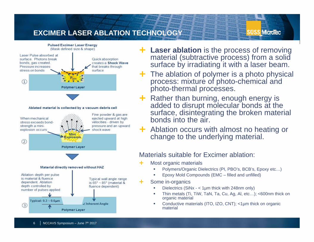
Laser ablation is the process of removing material (subtractive process) from a solid surface by irradiating it with a laser beam.
The ablation of polymer is a photo physical process: mixture of photo-chemical and photo-thermal processes.
Rather than burning, enough energy is added to disrupt molecular bonds at the surface, disintegrating the broken material bonds into the air.
Ablation occurs with almost no heating or change to the underlying material.
Materials suitable for Excimer ablation: Most organic materials
Polymers/Organic Dielectrics (PI, PBO’s, BCB’s, Epoxy etc…) Epoxy Mold Compounds (EMC – filled and unfilled)
Some in-organics Dielectrics (SiNx - < 1µm thick with 248nm only) Thin metals (Ti, TiW, TaN, Ta, Cu, Ag, Al, etc…); <600nm thick on
organic material Conductive materials (ITO, IZO, CNT); <1µm thick on organic
material
EXCIMER LASER ABLATION TECHNOLOGY
6 NCCAVS Symposium – June 7th 2017

NCCAVS Symposium – June 7th 2017
LASER ABLATION
7
What is Laser ablation? Direct Material Removal by laser irradiation Common Laser Types: CO2, DPSS (Diode Pumped Solid State), Excimer Various characteristics for different applications and purposes
Laser CO2 DPSS (Solid State) DPSS (Solid State) Excimer Excimer
Wavelength 10.6mm (long) 1.06um 355nm 308nm 248nm (short)
Photon Energy (eV) 0.12 1.7 3.5 4.08Breaks Bonds
5Breaks Bonds
Primary AblationMechanism
Thermal Thermal Thermal Photochemical Photochemical
Capable of Ablating or Cutting Matal Pads?
YES YES YES NO NO
Cu - Natural Stop Layer? Yes No No Yes Yes
Relative Laser Heat Classification
Heat Affected Zone (HAZ) & Recast
Large Moderate Moderate Small to none Small to none
In Production for Advanced Packaging?
Yes – LargeVias
Yes – Med Vias Yes – Med Vias Yes – small vias
No - Qualifying
Concerns of Pad/Dielectric Damage?
No – even though Thermal
No – even thoughThermal
No – even thoughThermal
Logically No –Less Thermal
+ Cu stop layer
Logically No –Less Thermal
+ Cu stop layer
HOT COLD

NCCAVS Symposium – June 7th 2017
Excimer Laser Ablation Solid State Laser Ablation
Imaging Type Mask based projection Maskless, direct ablation
Patterning area Field area, up to 50x50mm. 1000’s of features at a time
Single spot
Patterning Mode Direct bond breaking Melting and evaporation
Available wavelength (193nm), 248nm, 308nm Various: 355nm, 532nm, 1064nm, etc…
Throughput +++ (not dependent on pattern density) - (pattern density and shape dependent)
Typical applications Complex structures: Low density patterning, scribing, drilling:
Ablation of complex structures(i.e. RDL trench and vias)
Laser drilling(i.e. through glass vias)
Mask
Excimer Laser Large‐area Ablations
Solid State Laser Spot‐area Ablations
EXCIMER LASER STEPPER VS. SOLID STATE LASER
8

NCCAVS Symposium – June 7th 2017
SCAN BEAM ABLATION
9
Scanning Laser beam
Substrate moves under projection
lens to ablate next unit site
Process can be performed on wafers or substrates

NCCAVS Symposium – June 7th 2017
Typical setup of an Excimer Laser stepper: Laser beam is made uniform and shaped through the optics train The laser beam hits the mask, and the resulting image is projected through a reduction
projection optics on the substrate The system operates like a normal stepper, with a laser source instead of a UV lamp
SCHEMATIC SETUP OF AN EXCIMER LASER STEPPER
10

NCCAVS Symposium – June 7th 2017
Physical process of ablation is the generation of debris. Process breaks down the material molecular structure and debris is generated, simulating
dust. To maximize debris removal, a Debris Cell is used. Debris collection system sucks air around the ablation area Debris exhausted out of the building or through a filter Laminar flow of HEPA filtered air across the substrate.
Precious metals can be reclaimed!
DEBRIS COLLECTION
11
Debris Cell
Cu Pad (~3µm)
PI (~7µm)
Debris

NCCAVS Symposium – June 7th 2017
In addition to the debris cell, post-laser ablation cleaning is needed.
Depending on the ablated material, several options are available:
O2 plasma cleaning: RecommendedMost common cleaning methodSuccessful cleaning of wafer with PBO
(HD8820)
Sacrificial layer for debris removal:Successful removal process shown for FCPi
2100 (Fuji Film) Sacrificial layer removed using high-pressure CO2 ionized water
POST LASER ABLATION CLEANING
12
Post Ablation Post Cleaning

NCCAVS Symposium – June 7th 2017
OUTLINE
Advanced Packaging Trends
Excimer Laser Ablation Technology
Via and RDL Patterning in novel material
1
2
3
13
Reliability of Embedded Laser RDL Patterning
for Advanced Packaging4
NCCAVS Symposium – June 7th 2017
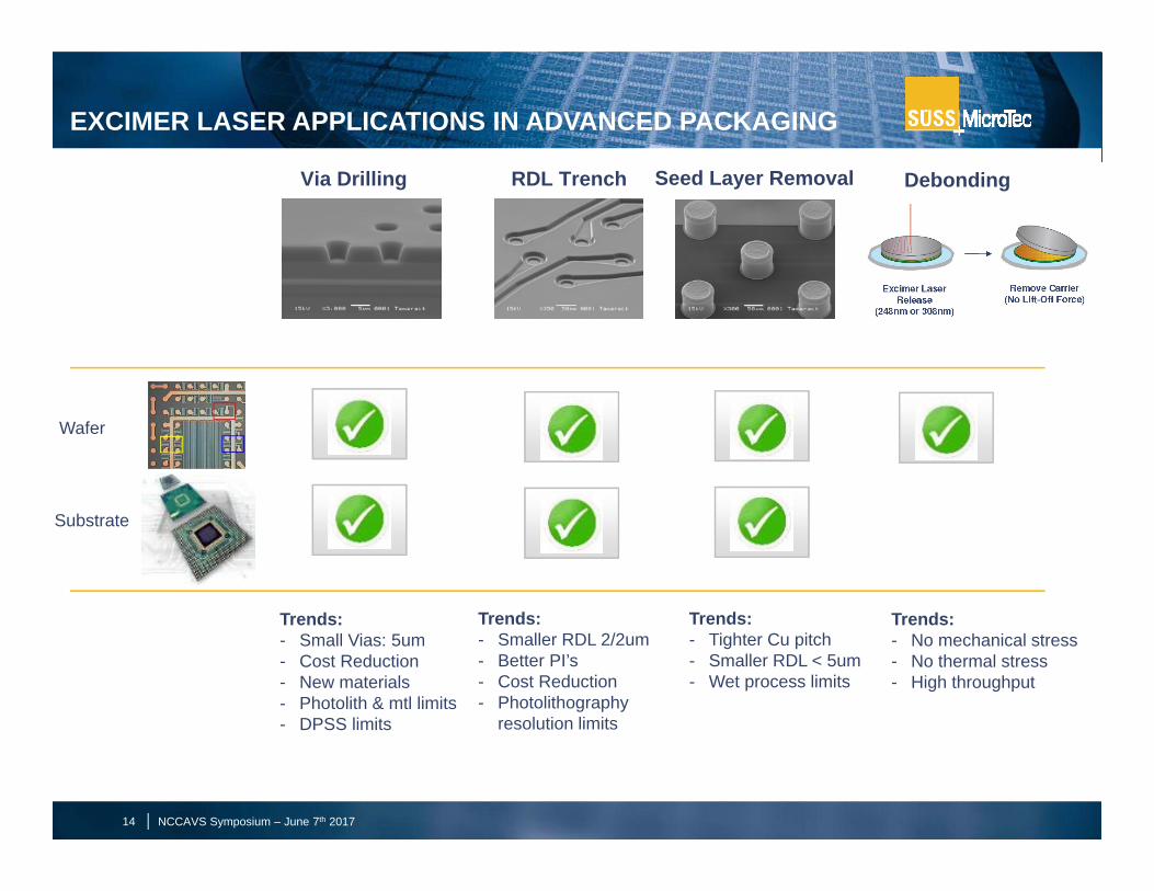
EXCIMER LASER APPLICATIONS IN ADVANCED PACKAGING
14
Via Drilling RDL Trench
Wafer
Substrate
Trends:- Small Vias: 5um- Cost Reduction- New materials- Photolith & mtl limits- DPSS limits
Trends:- Smaller RDL 2/2um- Better PI’s- Cost Reduction- Photolithography
resolution limits
Debonding
Trends:- No mechanical stress- No thermal stress- High throughput
Seed Layer Removal
Trends:- Tighter Cu pitch - Smaller RDL < 5um- Wet process limits
NCCAVS Symposium – June 7th 2017
EXCIMER ABLATION PROCESS CONTROL
15
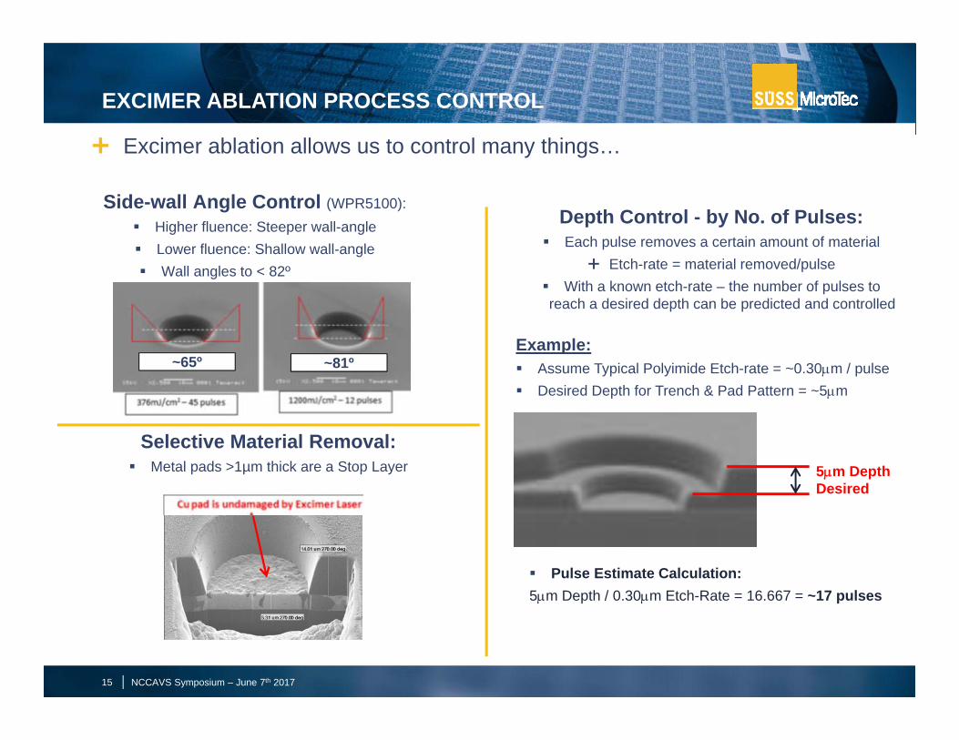
Excimer ablation allows us to control many things…
Side-wall Angle Control (WPR5100): Higher fluence: Steeper wall-angle Lower fluence: Shallow wall-angle Wall angles to < 82º
Depth Control - by No. of Pulses: Each pulse removes a certain amount of material
Etch-rate = material removed/pulse With a known etch-rate – the number of pulses to reach a desired depth can be predicted and controlled
Selective Material Removal: Metal pads >1µm thick are a Stop Layer
~65º ~81ºExample: Assume Typical Polyimide Etch-rate = ~0.30m / pulse Desired Depth for Trench & Pad Pattern = ~5m
5m Depth Desired
Pulse Estimate Calculation:5m Depth / 0.30m Etch-Rate = 16.667 = ~17 pulses

NCCAVS Symposium – June 7th 2017
Photolithography Limited Pitch and Via Wall Angle Control (UV Imaging) Flexibility desired to address tighter via pitches, wall angles for Cu sputtering or higher aspect ratios
where thicker dielectrics are desired.
Excimer Ablation Ablation performed after cure. Provides ability to flexibly alter the wall angle to the desired
requirement.
VIA PATTERNING LIMITATIONS - UV EXPOSURE PHOTO PI
16
BCB after UV expose BCB after Cure
Demonstration of via wall angle control: WPR5100 (7µm). Wall angle altered with fluence change9µm thick HD4000. Via wall angle 45 & 78 degrees
HD4000 – UV Imaged
9µm thick HD4000 &17µm via. Wall angle
~45 degrees
Photolithography
Wall to steep

NCCAVS Symposium – June 7th 2017
Excimer Laser Pulse #2
Unique Characteristic of Excimer Laser Ablation: Thick (>1m) Traces, Bumps & Pillars are Natural Stop Layers:
Consider the cross-section of the 1m tall Cu feature, below. The conductive metal immediately disperses the laser energy throughout the structure with
its sea of free electrons Any energy or heat that reached the Metal-Dielectric Interface is insufficient to break bonds
via photochemical or thermal action – so No melting or Ablation takes place – even with multiple pulses
Ti/Copper Layer (400nm)
1m tall feature
Excimer Laser Pulse #1
Photon Energy absorbed and dispersed
Photon Energy absorbed and dispersed
No AblationPolymer Layer (4m)
Silicon Wafer
RDL Feature on Copper Seed Layer on Polymer Dielectric
17
EXCIMER LASER SLR – SELECTIVE FOR THIN METAL SEED LAYER REMOVAL
No Ablation or Damage to RDL Structures Thicker than 1m - Readily apparent through
Laser Seed Layer Removal Ablations
Thick Cu Bumps Not Ablated or Damaged
Thin Seed Layer ablated off of Polymer

NCCAVS Symposium – June 7th 2017
MATERIAL ALTERNATIVE: NON-PHOTO DIELECTRICS
18
Photo vs. Non-Photo Dielectrics Non-Photo Dielectrics cost up to 50% LESS than Photo-Dielectrics Photo Dielectrics have a higher Shrinkage Rate – increased cost and less pattern fidelity Many Non-Photo Dielectrics have better thermal, mechanical and chemical properties Non-Photo Dielectrics increase the material choices => better CTE
$
+ 0.15 x $
Total Cost = ~1.15 $
Some Non-Photo Dielectrics have 30% less Shrinkage vs. Photo
11.5m
10m
AppliedThickness
Final Cured
Thickness
Assuming 15% Shrink Rate
Wafer
NON-PHOTO DIELECTRIC
$$
+ 0.45 x $$
Total Cost = ~3.0 $Almost 3X Cost
Assuming 45% Shrink Rate
14.5m
AppliedThickness
10m
Final Cured
Thickness
Wafer
PHOTO DIELECTRIC
NCCAVS Symposium – June 7th 2017
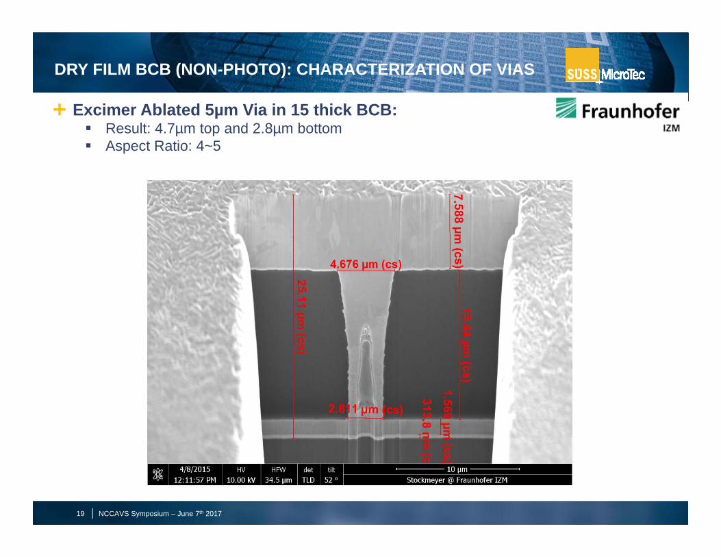
DRY FILM BCB (NON-PHOTO): CHARACTERIZATION OF VIAS
19
Excimer Ablated 5µm Via in 15 thick BCB: Result: 4.7µm top and 2.8µm bottom Aspect Ratio: 4~5

NCCAVS Symposium – June 7th 2017
LASER ABLATION OF BCB MATERIAL
0,000
1,000
2,000
3,000
4,000
5,000
6,000
7,000
8,000
9,000
10,000
0 5 10 15 20 25 30
Dep
th of a
blation [µm]
Number of pulses
4µm lines
10.6µm lines
4 µm vias
1P5P15P 10P20P30P
20

NCCAVS Symposium – June 7th 201721
5UM AND 10UM VIAS IN 9UM THICK NON-PHOTO ABF MATERIAL

NCCAVS Symposium – June 7th 201722
83°
FINE TRENCHES IN 5.6UM THICK HD4100: 2.0UM AND 2.5UM TOP OPENING
2um top via
2.5um top via
2.12um
1.14um
1.21um
2.43um
83o

NCCAVS Symposium – June 7th 2017
EFFECT OF FILLER SIZE ON FINE PITCH TRENCH FORMATION
2um 2um 2um
ABF GX92Large filler
ABF GY50Small filler
Fujifilm PolyimideNo filler
surface topology
4µmL/S
trench
- Large filler in polymer dielectrics leads to side erosion- Small/ no filler material enables high resolution trench formation
23
NCCAVS Symposium – June 7th 2017
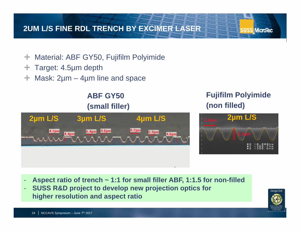
2UM L/S FINE RDL TRENCH BY EXCIMER LASER
Material: ABF GY50, Fujifilm Polyimide Target: 4.5µm depth Mask: 2µm – 4µm line and space
2µm L/S 3µm L/S 4µm L/S
- Aspect ratio of trench ~ 1:1 for small filler ABF, 1:1.5 for non-filled - SUSS R&D project to develop new projection optics for
higher resolution and aspect ratio
2µm L/S2.4µm
3.3µm
ABF GY50(small filler)
Fujifilm Polyimide(non filled)
24

NCCAVS Symposium – June 7th 2017
FINEST RDL TRENCH RESOLUTION
5/5um L/S in GX92
10um
3/3um L/S in GY50
6um
2/3um L/S in Polyimide
5um
Fine pitch embedded RDL trench wiring by Excimer Laser ablation
10µm pitch in GX92, 6µm pitch in GY50 and 5µm pitch in PI demonstrated
ABF GX92Large filler
ABF GY50Small filler
Fujifilm PolyimideNo filler
25

NCCAVS Symposium – June 7th 2017
FINE TRENCH IN FUJIFILM NON PHOTO MATERIAL
6/6, 5/5, 4/4, 3/3, and 2/2um L/S in PI demonstrated
Fujifilm Polyimide (FFEM)No filler
26
Fine pitch embedded RDL trench wiring by Excimer Laser ablation

NCCAVS Symposium – June 7th 2017
OUTLINE
Advanced Packaging Trends
Excimer Laser Ablation Technology
Via and RDL Patterning in novel material
1
2
3Reliability of Embedded Laser RDL Patterning
for Advanced Packaging4
27

NCCAVS Symposium – June 7th 2017
EMBEDDED LASER RDL FORMATION SCHEME
28

NCCAVS Symposium – June 7th 2017
Semi-additive Embedded trench
Cross section
Advantage- Current POR in industry- Lots of industry development
- No photo-lithography material required- Line & via formation in one Step- No wet seed removal required- Via pattern integrity
Challenge
- RDL Undercut and erosion during seed etch
- Surface non-planarity
- Planarization of Cu overburden
Fine line
- Erosion of the Cu during seed layer removal
- No Cu erosion
EMBEDDED LASER RDL FORMATION VS. CURRENT PROCESS
BU Layer
3 um L/S 3 um L/S
29

NCCAVS Symposium – June 7th 2017
Cu
SURFACE PLANARIZATION
20um
60um
Trench formationby excimer laser
Trench filling by Cu plating
Cu overburden removalby surface planarization
Polymer Polymer Polymer
30

NCCAVS Symposium – June 7th 201731
XSEM OF EMBEDDED RDL STRUCTURE IN FCPI 2100 (FUJI FILM)
40 micron pitch 52° tilt after FIB 40 micron pitch 90° tilt after FIB, high resolution detector
Courtesy of Fujifilm US
15/15/8um

NCCAVS Symposium – June 7th 2017
XSEM OF EMBEDDED LASER RDL IN PHOTO AND NON-PHOTO MATERIALS (VIA FIRST PROCESS)
32
• Material: LTC9320 low T cure (Fujifilm)• 4/4/4um L/S/via• Sputtering seed: 100nm Ti 600nm Cu• Cu Plating 4.7µm overburden• CMP for planarization (stop on seed layer)• Seed layer removal using Excimer Laser• No leakage observed post seed layer
removal• No plating voids in via!
• Material: ABF GY50 (Ajinomoto)• 6/6/6um L/S/via• Sputtering seed: 100nm Ti 600nm Cu• Cu Plating 4.7µm overburden• CMP for planarization for Cu, seed layer
and stop on ABF• No leakage observed post CMP• No plating voids in via!
Courtesy of IZM Fraunhofer

NCCAVS Symposium – June 7th 2017
AFFECT OF ABLATION ON METAL PAD/UNDERLYING METAL
3rd party confirmation of no damage to Cu pads
Excimer ablation over Cu and Al pads: 3rd party tests have been performed showing
no damage to the underlying materials Case study:
Si/SiOx/SiNx/TiTiN/AlCu(1.4um)/ dielectric(8.5um)
Over pulsed 40 and 50 with no damage to the low k dielectrics
33

NCCAVS Symposium – June 7th 2017
RELIABILITY DATA: MICRO VIA ABLATED BY EXCIMER LASER (ABF GX92)
34

NCCAVS Symposium – June 7th 2017
RELIABILITY OF EMBEDDED TRENCH (5/5UM)
Multilayer RDL structure in ABF GX92 with 8um via diameter20, 30 and 40um pitch daisy chain structureThermal shock testliquid to liquid: 125°C 1min and -55°C 1min
Top view Cross section view
No failure observed after 1000 cycle of thermal shock test
Courtesy of GIT-PRC
35

NCCAVS Symposium – June 7th 2017
Daisy-Chain contains over900 vias~150 Ohms
QUALITY CHECK OF LASER DUAL DAMASCENE RDL
Low temperature polyimid (Fujifilm LTC 9320)
36

NCCAVS Symposium – June 7th 2017
PROCESS COST COMPARISON
37
14x14mm package (10x10mm die), 10um via in 20um dielectric, 10/10um L/S RDL*
Photolithography ProcessCycle Time 5.80 hours
Excimer Laser ProcessCycle Time 2.38 hours Savings 59%
Photolithography ProcessCost/wafer ($USD) % of Total
Capital 44.64 60%Labor 1.37 2%
Material 27.93 38%Total 73.93 100%
Excimer Laser ProcessCost/wafer ($USD) % of Total
Capital 35.39 68%Labor 0.86 2%
Material(non‐photo dielectric) 15.45 30%
Total 51.70 100%Savings 30%
*Collaboration with SavanSys

NCCAVS Symposium – June 7th 2017
Excimer Laser Ablation is a Valuable Enabling Technology: Enables Finer Resolution Patterning in Photo-Polymers (Dielectrics) Enables Direct Dry-Etch Patterning of Non-Photo Polymers Enables Higher-Density Via Drilling Enables Multilayer RDL integration at lower cost Enables Complex Patterns, More Uniform Feature Shape, Placement and Quality on thin metal
surfaces Enables Selective Dry-Etch Thin Seed-Layer Removal Enables Cost-Effective Patterning of Large Surfaces
EXCIMER ABLATION – AN ENABLING TECHNOLOGY
Next GEN Device Patterning Challenges
Photolithography Limitations UV Lasers Limitations
BARRIERS
1. Fine Photo-Dielectric Patterning2. Direct Non-Photo Dielectric Patterning3. More Complex – Higher-Density Laser Patterning
Excimer Laser Ablation SOLUTIONS
Cu Pillar, Micro Bump, Solder Bump
RDL, Integrated Passives
Fan-Out WLP FCBGA, FCCSP2.5D Interposer,
3DIC
38

NCCAVS Symposium – June 7th 201739
SUSS MicroTec Photonic Systems, Inc.220 Klug CircleCorona, CA 92880-5409USA