F.# Maloberti: High%performance/ data/ converters:/...
6
F. Maloberti: "Highperformance data converters: Trends, process technologies and design challenges"; IEEE Asia Pacific Conf. on Circuits and Systems, APCCAS 2008, Macao, November 30December 3, 2008, pp. 1216. ©20xx IEEE. Personal use of this material is permitted. However, permission to reprint/republish this material for advertising or promotional purposes or for creating new collective works for resale or redistribution to servers or lists, or to reuse any copyrighted component of this work in other works must be obtained from the IEEE.
Transcript of F.# Maloberti: High%performance/ data/ converters:/...

F. Maloberti: "High-performance data converters: Trends, process technologies and design challenges"; IEEE Asia Pacific Conf. on Circuits and Systems, APCCAS 2008, Macao, November 30-‐December 3, 2008, pp. 12-‐16.
©20xx IEEE. Personal use of this material is permitted. However, permission to reprint/republish this material for advertising or promotional purposes or for creating new collective works for resale or redistribution to servers or lists, or to reuse any copyrighted component of this work in other works must be obtained from the IEEE.
High-Performance Data Converters: Trends,Process Technologies and Design Challenges
F. MalobertiDepartment of Electronics,
University of Pavia, ItalyEmail: [email protected]
Abstract— High-performance electronic systems use more andmore use high-performance data converters for improving andshaping the architecture and opening new application perspectives.The current and future trend depends on old and new factorsthat include global economy, technology evolution and marketing.All these elements are driving forces and create new challengesfor the designer that answer the requests of new applications byexploiting the advantages and limiting the drawbacks due to theamazing growth of process technologies.
I. INTRODUCTION
Data converters are essential gateways leading an analogsignal, which features many situations encountered in the real-world, to a digital format suitable for signal processing, datatransmission, computing and control; or, the other way around,data convertes transform a transmitted signal, a stored data, orthe product of digital processing into a real-world signal forcontrol, actuation, or further processing in the analog domain.
Data converters are increasingly important for system archi-tectures [1], [2], [3]. The strategy of many system designers isto move processing as much as possible to digital, as they relyon data converters able to provide high speed and large reso-lution. Moreover, the necessities of high-performance are oftenaccompanied by the need of low power consumption, or, morefrequently, the low-power feature is itself a key performanceand as a result speed and resolution become trade-off elementstogether with silicon area and cost.
The design [4] and fabrication of data converters follow (or, insome cases, must follow) the evolution of process technologies,but also exploit other advancements like the ones of specialtechnologies and packaging. Thanks to them, in some criticalsituations, ultra-thin line-width technologies with very low sup-ply voltages can be avoided and optimum performance obtained.
This paper considers first previous trends and the resultingapplications. Then, it derives the most important features of therecent high-performance data converters. The process technologyand its advantages and limits are examined for identifying thechallenges that the designer faces. Finally, emerging designdirections are discussed.
II. HISTORY AND TREND
Two factors mainly drove the data converter development:technology and applications. It is well known that technologyevolved with the incredible pace predicted by the so-calledMoore Law [5], that foresees a doubling of the circuit complexity
and a reduction of a factor two of the transistor line-width every18 months. However, the sector that derived the major advan-tages is the digital processing and digital storing of data. Theanalog area, by contrast, suffered by various drawbacks that cannot be fully compensated by the benefits of technology shrinking.Therefore, analog designers preferred using mature technologyand to move to thinner line-width only when economical reasonsor system integration needs forced to do that. Nevertheless, evenwith a delay, analog circuits and data converters followed theevolution of process technology.
The technology used by an electronic system mainly de-pends on its required specifications: for very high speed andnon demanding analog performance nanometer technologies arebeneficial. For example, a current steering DAC only requiresa reasonable matching between current sources whose outputresistance must be large; since the key feature of the DAC is thespeed of operation, for resolutions in the 10!!14 bit range, theuse of the most advanced technologies benefits the conversionrate. It is reasonable to predict that the data conversion ratefor medium resolution will increase by almost two decadesin approximately 10 years from now. On the contrary, dataconverters for sensors, that must ensure resolutions of 18bitor more, still prefer mature technologies and benefit from theprecision qualities.
Recently, the trend is to incorporate data converters with largedigital sections, but the designers compliance is at significantlydifferent speed for dissimilar applications and markets. Therecent history of data converters can be dated back to 90swhen the major data converter applications were instrumentation,measurement, industrial process control, medical imaging, audioand video. At that time, communication field was in an initialphase of development and all the apparatuses were pluggedwithout low power requirements. Later, the communicationmarket became a big driving force for low-cost, medium-power,high-performance data converters, that were used in modems,and wireless infrastructure (base stations). Even for those ap-plications, low power was not a pressing request, but shortlylater the cell phone handset and other portable battery-poweredapplications emphasised the need of lower power and single-supply voltages. Therefore, the use of lower voltage CMOSprocesses was a proper choice because the reduced supplyvoltages allowed higher speed. However, the lower signal rangeand the almost unchanged headroom made the designs moresensitive to noise. Nevertheless, for medium resolution and wide
12978-1-4244-2342-2/08/$25.00 ©2008 IEEE.
Authorized licensed use limited to: UNIVERSITY OF PAVIA. Downloaded on March 25, 2009 at 11:35 from IEEE Xplore. Restrictions apply.

Fig. 1. Evolution of the first generation packages.
bandwidth data conversions, the use of the same technology thatis also used by digital processors became the general trend. Also,the utilization of the sigma delta technique, that trades speedwith accuracy, permits to obtain an increasing signal band withmedium resolution (60! 75 dB).
The use of the same technology in high resolution systems(80 dB or more) is problematic and rarely pursued: instead, it ismore viable to use the optimum technology (like the BiCMOSor the SiGe ones) for the analog part and realize a multiple chipsystem. The packaging trend facilitates the approach. Packagingevolved from the first generation (Fig. 1) that started fromthe traditional DIP of the early times to smaller and smallerfootprints that enable the surface mount packages which aresuitable for high-volume automatic mass-assembly manufactur-ing techniques. The modern packages include both leaded typesand non-leaded types such as the laminated substrate package orball grid array (BGA). More recently 3D packages (stack dice,stack package and system in package, SiP) were introduced.
III. CONVERTER APPLICATIONS
Almost all the systems that process signals of the real worduse data converters. The ones that require high-performancecan be classified into three categories: high-precision systems,software defined systems, and portable or autonomous systems.The features and key performances are resumed below.
A. High-Precision SystemsApplications in the field of open and closed loop industrial
process control, robotics, medical instrumentation, test and dataacquisition systems need ADCs and DACs with high accuracy(16-bit or more). For those applications the speed is not impor-tant as the signal band is often in the range of tens of kHz [6];by contrast, it is essential ensuring clean supply and referencevoltages, an excellent component matching and a good drivingcapability.
B. Software De ned SystemsThe most important application of this category is the software
defined radio [7] which is the current trend for communicationsystems. The data converters are the endings of the processing
chain for permitting different processing required by variousarchitectures. The same concept is extended to other needs.Therefore, for data converters used in software defined systems,wide bandwidth is essential. The required number of bit dependson the standard and the current trend is to limit the resolutionat the expenses of a relatively larger signal band.
C. Portable and Autonomous Systems
An increasing number of electronic systems become portableand nomadic. For these applications the main concern is tohave a long battery life and, more frequently, to harvest energyand to operate without external refueling. Therefore, low poweris very important and, often, some of the above mentionedperformance, are constrained for an higher power effectivenesswhich is quantified by the figure of merit (FoM), that links thepower, Ptot, the effective number of bit, ENoB and the signalband, fB , defined as
FoM =Ptot
2ENoB2fB. (1)
Modern systems demand for a data converter capable to obtainFoM in the ten of fJ-conv-level for signal band in the hundredsof KHz to MHz range [8], [9].
IV. PROCESS TECHNOLOGY
The IC complexity increases continuously [10] thanks to thecontinued improvements in optical projection lithography byabout 30% every two years. Process technology is now in sub-wavelength mode where extreme Ultra-Violet (EUV) lithographyobtains the patterning of lines below 30 nm dimensions. At thesame time, the minimum feature size, oxide thickness, supplyvoltage and transistor thresholds diminish for controlling variousshort channel effects like the VTh roll-off or the Drain-InducedBarrier Lowering (DIBL).
One of the major problems of ultra-thin technology is gateleakage caused by direct band-to-band tunneling. Moreover,highly energetic carries generate electron-hole pairs leading tocharges trapped in the oxide, causing a steadily increase in thetunneling current until, in the end, the oxide breakdown occurs.Moreover, the threshold voltage steadily degrades.
Another important limit comes from the reduction of thesupply voltage that, on one hand, lowers the power dissipation,but, on the other hand, degrades the signal-to-noise ratio (SNR)of analog circuits. Moreover, low thresholds enhance the leakageand this dissolves signals stored on capacitors. A possible(expensive) remedy, is using dual threshold technologies whenthe high threshold devices have low leakage.
The above points indicate that the push toward deep sub-micron technology is not very attractive for analog functionsthat, when implemented alone or with a small digital part, aremore conveniently obtained with analog technologies whoseline-width is 2–3 times larger than digital applications. The chal-lenge is for large digital systems integrated in deep submicrontechnologies with few analog functions (mainly data converters).
13
Authorized licensed use limited to: UNIVERSITY OF PAVIA. Downloaded on March 25, 2009 at 11:35 from IEEE Xplore. Restrictions apply.

0 0.1 0.2 0.3 0.4 0.5 0.6 0.7 0.810
3
104
105
106
Lenght [ ]
Outp
ut re
sis
tance [ Ω
]
Output Resistance
µ
k/L
Fig. 2. Output resistance decrease for low channel length.
V. CONSEQUENCES OF SCALING ON ANALOG
In the next 5–10 years the transistor line-width will become35–22 nm with 1–1.5 nm equivalent oxide thickness. The VDD,limited by reliability consideration, will drop below 1 V [2].Therefore, especially for analog, it will be important usingoxides with high field strength for higher supply voltages. Inaddition to the low supply voltage other factors limit the analogperformance.
A. Transconductance
With very short channels the carrier velocity quickly reachesthe saturation limit, the transconductance saturates and becomesindependent on gate length or bias, as approximated by
gm =WeffCoxvsat
2. (2)
A low transconductance is not desirable for analog design:for obtaining high gain it is necessary to use wide transistorsthus augmenting parasitic capacitances and, in turn, reducingbandwidth and slew rate.B. Output Resistance
Even the output resistance is affected by shrinking and quicklydecreases when the gate lengths becomes lower than 0.1µm(much faster than L, Fig. 2). The reduction of the outputresistance and the saturation of gm affect the intrinsic gain: witha given transconductance limit, when the output resistance r0
becomes 1/gm, the intrinsic gain gmr0 is unity and the devicecannot be used anymore for amplification purposes. Obtainighigh gain is more and more problematic as using cascodestructures with stack of transistors reduces the signal swing.
C. Diffusion and Gate Capacitances
Scaling makes the gate oxide thinner; therefore, the specificcapacitance Cox increases as function of the shrinking factor.Since the gate area can be made smaller, parasitics remainconstant or diminish as the process shrinks. However, inter-connections use thick and close metals whose parasitics maybecome dominant. Therefore, globally, modern technologies are
100101
100
10
1
0.1
Si-Ge BiCMOSBiCMOS
CMOS
fT (GHz)
Su
pp
ly V
olta
ge
[V
]
Fig. 3. Supply voltage versus the technology unity gain frequency.
not much beneficial in moving non-dominant poles at highfrequencies.
D. Matching AccuracyThe offset of any analog circuit and the static accuracy of
data converters depend on the matching between nominallyidentical devices. The stochastic nature of physical and chemicalfabrication steps causes a random time-independent differencebetween equally designed elements. The stochastic mismatchbetween corresponding parameters p of close elements is
!(!p)2 =A2
p
W L+ S2
pd2 (3)
where Ap and Sp are matching parameters at unity area andunity distance, d is the distance between the centroids of thetwo identically designed elements. Typically, for preservingmatching, the area of transistors or capacitors must diminishas a function of the shrinking factor, while the area of resistorsshould diminishes less because of the perimetrical term.
E. Signal SwingThe shrink of processes reduces the supply voltage. Since it is
necessary to ensure a suitable headroom for keeping transistorsin saturation, the minimum swing of signals cannot be close toVDD or ground by more than about 100 mV . Therefore, the trendshown in Fig. 3 predicting CMOS supply voltages well below1 V in the next few years conceives signal swing as small asfew hundred mV. More expensive technologies like the BiCMOScan become competitive for high precision data converters. Lowvoltage is also problematic for driving CMOS switches as theon-resistance can become very high or at the limit the switchdoes not close at all in some interval of the input amplitude.
VI. DESIGN CHALLENGESThe changing features of process technologies challenge the
design of high-performance data-converters especially with highaccuracy. For high-precision convertes, the main difficultiescome from
• the design and the integrity of reference voltages;• the rejection of interferences coming from the digital sec-
tions.
14
Authorized licensed use limited to: UNIVERSITY OF PAVIA. Downloaded on March 25, 2009 at 11:35 from IEEE Xplore. Restrictions apply.

For high speed [11][12] the technology trend is favourable,but the velocity saturation in very short channel that limits thetransconductance gain imposes higher current in amplifiers. Thereduction of the supply voltage also diminishes the referencevoltage of the converter and, in turn, scales the amplitude of thequantization steps.
Another challenge to high speed conversion comes from theclock jitter. As known a gaussian uncertainity in the clock "jitgives rise to a noise power
v2n,ji =
(2#finAin)2
2"jit
2 (4)
where Ain is the amplitude of an input sine wave at fin. Usingthe maximum amplitude VRef/2 and assuming that the jitterpower equals to the one of the quantization (loss of 0.5-bit), itis possible to obtain the diagram of Fig. 4 that gives the requiredjitter versus the resolution at different input frequencies.
Notice that for resolutions in the 10-bit range requires clockjitter of few hundred of psec for signals below 200 MHz whichis difficult to obtain. For higher frequencies it is necessary toensure clock jitters in the tens of psec range.
Therefore, the design of high-speed converters, albeit facili-tated by the technology, engages the designer for
• sustaining the SNR;• designing high-gain OTAs;• reducing the limits caused by the CMOS switches,• properly handling the clock for a minimum jitter degrada-
tion.The low-power data converters use relatively low conversion
frequency and mature technologies [8], [9]. When the samplingrate increases and thin line-width technologies are used, thepower effectiveness significantly decreases. There is a combina-tion of negative effects that includes the reduced supply voltagethat imposes bigger sampling capacitors, the augmented biascurrent necessary to increase the transconductance gain and theshort channel effects that diminish the transconductance and thedc gain effectiveness. All these factors can be accounted for ina behavioral model that gives the results as predicted in Fig.
8 9 10 11 12 13 1410
!3
10!2
10!1
100
101
N!bit
Clo
ck J
itte
r [p
sec]
25 MHz
50 MHz
100 MHz
200 MHz
400 MHz
800 MHz
Fig. 4. Required clock jitter at different resolutions and bandwidths.
! "!! #!! $!! %!! &!! '!! (!! )!!"!
!$
"!!#
"!!"
"!!
"!"
*+,-./0123+4526789:
;<=5>26?:
2
2
"!!@/4
""!@/4
"#!@/4
Fig. 5. Estimated power consumption of ADC versus the conversion speed.
5. A state-of-the-art 10 bit pipeleine converter that consumesabout 5mW at 100MS/s increases the power by a factor 30for augmenting the sampling rate by 8. The simulation giveseven worse figures for higher resolutions. Therefore, we have toexpect a significant reduction of the FoM for high speed, high-performance data converters.
The challenges for the designer in this area are• the use of algorithms that do not need active devices;• the design of wide-swing OTAs;• the invention of techniques that allow using supply voltages
higher than the technology limit.
VII. DESIGN DIRECTIONS
The design challenges are faced with various strategies that, inaddition to what mentioned before, follow new design directions.
A. New Algorithms and Architectures
The need of data conversion gave rise to numerous algorithmsadapted to a given technology. Moreover, many of the inventedalgorithms become eventually obsolete because of the technol-ogy evolution. As outlined, there are limitations in obtainingdesired performance and the solution can be the attempt to obtainthose performance with the evolving technology or to inventnew algorithms or new architectures that fit the advantageousfeature of the new processes. Since speed is one of the keyadvantages, methods that trade speed with other paramenters aregood candidates for future developments [13–18].
B. Use of Parallelism
A method that helps in reducing the power consumption is theuse of interleaved structures. The same can be used to improvethe accuracy by averaging the results. The cost of using schemesworking in parallel for processing the same input becomesnegligible for the decresing cost per transistor. Therefore, newconversion methods that use a massive parallelism can becomefeasible in the near future [19][20].
15
Authorized licensed use limited to: UNIVERSITY OF PAVIA. Downloaded on March 25, 2009 at 11:35 from IEEE Xplore. Restrictions apply.
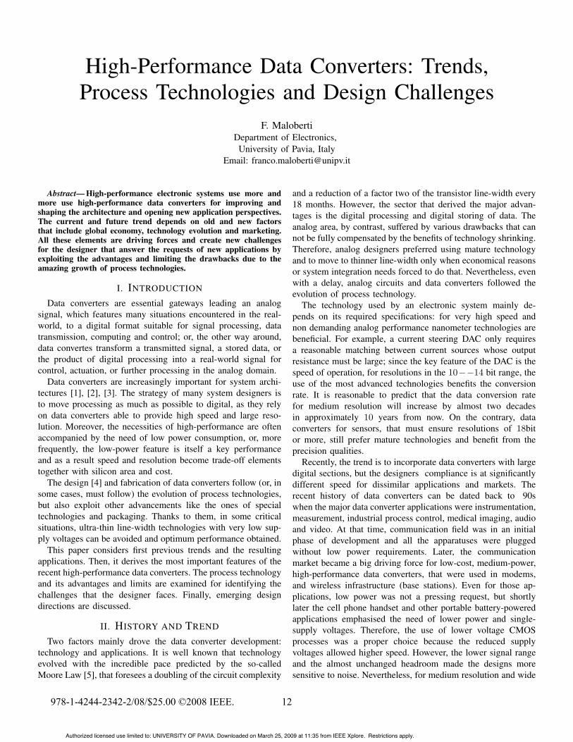
Fig. 6. System in package with wired bonded and embedded in the substratedies.
C. Use of Multi-rate SolutionsThe present distinction between Nyquist rate and oversampled
methods will become softer as the high-speed processing capa-bility can be exploited in section of architectures for answeringsome special request. The resulting multi-rate architectures canobtain, for example, relaxed anti-aliasing specifications or focuson segment of the signal band.
D. Digitally Assisted AnalogThe limitations of analog features are more and more cor-
rected with digital techniques. Presently, digital processorssupport calibration algorithms for improving the matching ofelements and static linearity. The approach will be extended forimproving the performance of analog sections. For example, theoutput dynamic of analog cells can be expanded by a digitallycontrolled dynamic level shifting. Architectures can be digitallyreconfigured for an optimum use of power and so forth[21-24].
VIII. CONCLUSIONS
The future of data conversion is full of expectations andchallenges. Modern systems, either on chip or in package,possibly using advanced packaging techniques [25] like the oneillustrated in Fig. 6 that enables a exible system partitioning and3D integration, will base their architecture and performance onthe data converter that they have on board. The collaboration ofsystem architects and analog circuit designers will be the drivingforce of future research and development.
ACKNOWLEDGMENT
The author would like to thank FIRB, Italian National Pro-gram #RBAP06L4S5 for partial economical support.
REFERENCES
[1] Counts l., “Analog and Mixed-Signal Innovation: The Process- Circuit-System-Application Interaction”. IEEE International Solid-State CircuitConference, ISSCC, Vol. 50 pp. 26 – 29. 2007
[2] van Roermund, A.H.M., ”Smart, exible, and future-proof data converters”,18th European Conference on Circuit Theory and Design, ECCTD, pp. 308– 319, 2007.
[3] Robertson D., ”The Past, Present, and Future of Data Converters and MixedSignal ICs: a Universal Model” . IEEE Symposium on VLSI Circuits, pp. 1– 4, 2006.
[4] F. Maloberti, “Data Converters”, Springer Ed., Dordrecht, The Netherland,2007.
[5] Moore, G. E., “Cramming more components onto integrated circuits”,Electronics, Vol. 38, n. 8 April 19, 1965.
[6] V. Quiquempoix, P. Deval, A. Barreto, G. Bellini, J. Markus, J. Silva, andG. C. Temes, ”A low-power 22-bit incremental ADC,” IEEE Journal ofSolid-State Circuits, vol. 41, pp. 1562 – 1571, 2006.
[7] Walter H.W. Tuttlebee (Editor), ”Software Defined Radio: Enabling Tech-nologies” Wiley Interscience, 2002.
[8] M. D. Scott, B. E. Boser, ard K. S. J. Pister, “”An Ultralow-Energy ADCfor Smart Dust”, IEEE J. Solid-State Circuits, vol. 38, no. 7, pp. 1123 –1129, 2003.
[9] Agnes, A. Bonizzoni, E. Malcovati, P. Maloberti, F. “A 9.4-ENOB 1V 3.8µW 100kS/s SAR ADC with Time-Domain Comparator”. IEEE InternationalSolid-State Circuit Conference, ISSCC, Vol. 51 pp. 246 – 247, 2008.
[10] Matsuzawa, A., “Analog IC technologies for future wireless systems”,IEICE Trans. Electron, Vol. E89-C, pp. 446 – 454, 2006.
[11] Ginsburg, B.P.; Chandrakasan, A.P., “Highly Interleaved 5b 250MS/s ADCwith Redundant Channels in 65nm CMOS”, IEEE International Solid-StateCircuit Conference, Vol. 51 pp. 240 – 241, 2008.
[12] S. Mehta, W. W. Si, H. Samavati, M. Terrovitis, M. Mack, K. Onodera, S.Jen, S. Luschas, J. Hwang, S. Mendis, D. Su, and B. Wooley, ”A 1.9GHzsingle-chip CMOS PHS cellphone” IEEE International Solid-State CircuitsConference, vol. XLIX, pp. 484 – 485, 2006.
[13] S. K. Gupta, M. A. Inerfield, and J. Wang, ”A 1-GS/s 11-bit ADC with55-dB SNDR, 250-mW power realized by a high bandwidth scalable time-interleaved architecture,” IEEE Journal of Solid-State Circuits, vol. 41, pp.2650 - 2657, 2006.
[14] S. Shahramian, A. C. Carusone, and S. P. Voinigescu, ”Design methodologyfor a 40-Gsamples/s track and hold amplifier in 0.18-m SiGe BiCMOStechnology,” IEEE Journal of Solid-State Circuits, vol. 41, pp. 2233 - 2240,2006.
[15] G. Manganaro, S. Kwak, and A. R. Bugeja, ”A dual 10-b 200-MSPSpipelined D/A converter with DLL-based clock synthesizer,” IEEE Journalof Solid-State Circuits, vol. 39, pp. 1829 - 1838, 2004.
[16] Shen, D.-L., Lee, T.-C, “A 6-bit 800-MS/s Pipelined A/D Converter WithOpen-Loop Amplifiers”, IEEE Journal of Solid-State Circuits, Vol. 42 pp.258 – 268, 2007.
[17] G. Mitteregger, C. Ebner, S. Mechnig, T. Blon, C. Holuigue, and E.Romani, ”A 20-mW 640-MHz CMOS continuous-time !" ADC with 20-MHz signal bandwidth, 80-dB dynamic range and 12-bit ENOB,” IEEEJournal of Solid-State Circuits, vol. 41, pp. 2641 – 2649, 2006.
[18] Mercer, D.A, “Low-Power Approaches to High-Speed Current-SteeringDigital-to-Analog Converters in 0.18-mum CMOS”, IEEE Journal of Solid-State Circuits, Vol. 43 pp. 1688 – 1698, 2008.Vol. 2 pp. 191 – 201, 2008.
[19] Asemani, D., Oksman, J., Duhamel, P., “Subband Architecture for HybridFilter Bank A/D Converters”, IEEE Selected Topics in Signal Processing,Vol. 2 pp. 191 – 201, 2008.
[20] Cheng-Chung Hsu, Fong-Ching Huan, Chih-Yung Shih, Chen-Chih Huang,Ying-Hsi Lin, Chao-Cheng Lee, Behzad Razavi, ”An 11b 800MS/s Time-Interleaved ADC with Digital Background Calibration”,” IEEE InternationalSolid-State Circuits Conference, vol. XLX, pp. 464 – 465, 2007.
[21] Blecker, E. B., McDonald, T. M., Erdogan, O. E, Hurst, P. J and Lewis,S. H., “Digital background calibration of an algorithmic analog-to-digitalconverter using a simplified queue”, IEEE Journal of Solid-State Circuits,vol. 38, pp. 1059 – 1062, 2003.
[22] Chan, K. L., Zhu, J.; Galton, I., “Dynamic Element Matching to PreventNonlinear Distortion From Pulse-Shape Mismatches in High-ResolutionDACs”, IEEE Journal of Solid-State Circuits, Vol. 43 pp. 2067 – 3078,2008.
[23] M. Daito, H. Matsui, M. Ueda, and K. Iizuka, ”A 14-bit 20-MS/spipelined ADC with digital distortion calibration,” IEEE Journal of Solid-State Circuits, vol. 41, pp. 2417 – 2423, 2006.
[24] K. Iizuka, H. Matsui, M. Ueda, and M. Daito, ”A 14-bit digitally self-calibrated pipelined ADC with adaptive bias optimization for arbitraryspeeds up to 40 MS/s,” IEEE Journal of Solid-State Circuits, vol. 41, pp.883 – 890, 2006.
[25] H. Reichl, A. Ostmann, R. Wieland, and P. Ramm, ”The third dimensionin microelectronics packaging,” Proc. 14th Eur. Microelectronics PackagingConf. Exhibition, p. 1 – 4, 2003.
16
Authorized licensed use limited to: UNIVERSITY OF PAVIA. Downloaded on March 25, 2009 at 11:35 from IEEE Xplore. Restrictions apply.