
F-Cue/ F-Cue EXTENSION BOARD Hardware Manual - · PDF file · 2017-05-26F-Cue/...
67
©2017 FUJITSU ELECTRONICS INC. 1/67 F-Cue/ F-Cue EXTENSION BOARD Hardware Manual Rev.1.02 2017/05/18 FUJITSU ELECTRONICS INC.
-
Upload
truongdang -
Category
Documents
-
view
253 -
download
9
Transcript of F-Cue/ F-Cue EXTENSION BOARD Hardware Manual - · PDF file · 2017-05-26F-Cue/...
©2017 FUJITSU ELECTRONICS INC. 1/67
F-Cue/ F-Cue EXTENSION BOARD
Hardware Manual
Rev.1.02 2017/05/18
FUJITSU ELECTRONICS INC.
Hardware Manual
2/67 ©2017 FUJITSU ELECTRONICS INC.
1. The contents of this document may be changed without prior notice. Please verify with our sales department if you need
any assistance.
2. The data and circuits given in this document are merely examples of using the semiconductor device and are not
intended for installation in equipment that actually used. Further, our company does not bear any liabilities whatsoever
regarding any third patent right violations or other rights violations arising out of the use of these data and circuits.
3. Transferring or copying the contents of this document without prior written permission from our company is prohibited.
4. The semiconductor devices of our company are intended for use in standard applications (office equipment such as
computer, OA, etc., equipment related to industrial, communication, measurement, equipment for personal or home use,
etc.). Customers considering use in special applications (aircrafts, space, nuclear power control, life sustaining medical
applications, etc.) such as in equipment wherein any fault or wrong operation of these semiconductors can directly cause
a threat to human life, or is likely to cause damage to human body, or wherein extremely high reliability is required are
requested to consult our sales department before using.
5. Failures of semiconductor devices occur at certain probabilistic rates. The customers are requested to carry out safety
designs such as equipment redundancy design, fire spreading countermeasure design, overcurrent prevention
countermeasure design, wrong operation prevention design, etc., so that, even if our company’s semiconductor device
fails, as a result human injury accidents, fire accidents, and accidents causing social damage do not occur.
6. When the product described in this document comes under the goods or technology restricted under the Foreign
Exchange and Foreign Trade Act of Japan, permission from the concerned authority is required at the time of exporting
this product.
©2017 FUJITSU ELECTRONICS INC. Printed in Japan
Hardware Manual
©2017 FUJITSU ELECTRONICS INC. 3/67
Contents
1. Introduction ........................................................................................................................................................................................................... 6
2. What's in the Box ................................................................................................................................................................................................. 8
2.1. F-Cue ................................................................................................................................................................................................................ 8
2.2. F-Cue EXTENSION BOARD (OPTION) ................................................................................................................................................ 9
3. Board Overview.................................................................................................................................................................................................. 10
3.1. Key Components .......................................................................................................................................................................................... 10
3.2. System Block Diagram ............................................................................................................................................................................... 12
3.3. Switch Configuration .................................................................................................................................................................................. 13
3.3.1. Boot Mode selection (DIP-SW) ...................................................................................................................................................... 13
4. Getting Started.................................................................................................................................................................................................... 14
4.1. Prerequisites ................................................................................................................................................................................................. 14
4.2. Known Limitations ...................................................................................................................................................................................... 14
4.3. First Power ON ............................................................................................................................................................................................ 14
5. Component Detail .............................................................................................................................................................................................. 15
5.1. Processor ....................................................................................................................................................................................................... 15
5.2. PMIC .............................................................................................................................................................................................................. 15
5.3. Memory/Storage .......................................................................................................................................................................................... 15
5.3.1. LPDDR3 ............................................................................................................................................................................................... 15
5.3.2. eMMC ................................................................................................................................................................................................... 17
5.3.3. SD Card ................................................................................................................................................................................................. 18
5.3.4. HSSPI .................................................................................................................................................................................................... 20
5.4. Networking .................................................................................................................................................................................................... 21
5.4.1. WLAN/ BT ........................................................................................................................................................................................... 21
5.5. Display Interface.......................................................................................................................................................................................... 23
5.5.1. HDMI .................................................................................................................................................................................................... 23
5.5.2. MIPI DSI ............................................................................................................................................................................................... 25
5.6. USB Ports ...................................................................................................................................................................................................... 26
5.6.1. USB3.0/2.0 Host ................................................................................................................................................................................. 26
5.6.2. USB2.0 Device .................................................................................................................................................................................... 28
5.7. Audio ............................................................................................................................................................................................................... 30
5.7.1. I2S ........................................................................................................................................................................................................... 30
5.8. DC Power ...................................................................................................................................................................................................... 31
5.9. Power Measurement ................................................................................................................................................................................... 31
Hardware Manual
4/67 ©2017 FUJITSU ELECTRONICS INC.
5.10. External Fan Connection ........................................................................................................................................................................ 32
5.11. UART ............................................................................................................................................................................................................ 32
5.12. Buttons ......................................................................................................................................................................................................... 33
5.12.1. POWER Switch ................................................................................................................................................................................ 33
5.12.2. WAKEUP Switch ............................................................................................................................................................................. 34
5.13. LED Indicators .......................................................................................................................................................................................... 35
5.13.1. User LED ............................................................................................................................................................................................ 35
5.14. I2C ................................................................................................................................................................................................................ 36
5.15. External I/F (GPIO) ................................................................................................................................................................................. 38
5.16. Additional Functionality .......................................................................................................................................................................... 39
5.16.1. PCIe ..................................................................................................................................................................................................... 39
5.16.2. Ethernet ............................................................................................................................................................................................... 40
6. Extension Connectors ....................................................................................................................................................................................... 41
6.1. Low Speed Extension Connector ............................................................................................................................................................. 42
6.2. High Speed Extension Connector ............................................................................................................................................................ 43
6.3. Giga Speed Extension Connector ............................................................................................................................................................ 44
7. Clock ....................................................................................................................................................................................................................... 45
8. Reset ....................................................................................................................................................................................................................... 47
9. Power Management Overview ...................................................................................................................................................................... 49
9.1. DC Power Input ........................................................................................................................................................................................... 49
9.2. Block Diagram ............................................................................................................................................................................................. 50
9.3. Power Sequencing ....................................................................................................................................................................................... 51
9.4. Power Supplies ............................................................................................................................................................................................. 51
10. Mechanical Specification .............................................................................................................................................................................. 52
10.1. F-Cue Dimensional Drawing ................................................................................................................................................................. 52
10.2. F-Cue EXTENSON BOARD Dimensional Drawing ........................................................................................................................ 54
11. Appendix ............................................................................................................................................................................................................. 56
11.1. Pinmux List ................................................................................................................................................................................................. 56
12. F-Cue EXTENSION Board (Option) ....................................................................................................................................................... 57
12.1. Prerequisites ............................................................................................................................................................................................... 57
12.2. Assembly Drawing .................................................................................................................................................................................... 57
12.3. First Power ON ......................................................................................................................................................................................... 58
Hardware Manual
©2017 FUJITSU ELECTRONICS INC. 5/67
12.4. Hardware Specification ........................................................................................................................................................................... 58
12.5. Block Diagram ........................................................................................................................................................................................... 59
12.6. Component Details ................................................................................................................................................................................... 60
12.6.1. Ethernet ............................................................................................................................................................................................... 60
12.6.2. PCIe ..................................................................................................................................................................................................... 63
12.6.3. Extension UART ............................................................................................................................................................................... 65
Hardware Manual
6/67 ©2017 FUJITSU ELECTRONICS INC.
1. Introduction
F-Cue is a miniature CPU board compliant with a 96Boards specification and is equipped with Socionext Inc.'s MB86S71 high
performance ARM processor.
In addition to the 96Boards specification interface, you can use the LAN and PCIe interfaces by connecting Fujitsu Electronics's
F-Cue EXTENSION BOARD (sold separately) to F-Cue.
The following table shows the general specifications.
Table 1-1 General Specifications
No. Item Description Remarks
1 Board name F-Cue
F-Cue EXTENSION BOARD
2 Board type MSB7701-C01 (F-Cue)
MSB7701-E01 (F-Cue EXTENSION BOARD)
3 Processor
Socionext MB86S71
ARM Cortex-A15 x 2 (1.2GHz), Cortex-A7 x 2 (825MHz)
ARM Mali-T624
4 Memory/Storage
2GB LPDDR3 1333MHz
16GB eMMC 4.51
SD 3.0 UHS-I/DDR50 (micro SD card slot)
5 Video/Image
Multi Standard Encode
2 stream H.264 Decode
32k x 32k JPEG CODEC
6 Network WLAN 802.11 ac/a/b/g/n
Bluetooth 4.2
7 External interface
USB2.0 x 1 microB (Device)
USB2.0 x 1 / USB3.0 x 1 Type-A (Host)
HDMI 1.4b (Tx)*1
8 Extension connector
Low speed 40-pin connector:
UART, SPI, I2C, PCM/I2S, GPIO
High speed 60-pin connector:
MIPI DSI, USB2.0, SPI, I2C
Giga speed 60-pin connector:
Gigabit Ethernet, PCI Express Gen2
Hardware Manual
©2017 FUJITSU ELECTRONICS INC. 7/67
9 Operating ambient
temperature 0 to 70°C
The CPU's internal temperature
shall not exceed the rating
(110°C)
10 Operating ambient
humidity 0 to 70% RH, No condensation
11 Power supply
+12V (+-5%) 2.0A
DC Jack: Supplied from the PJ-041H (1.65 mm center pin
diameter)
A separate AC adapter is
required
12 Board dimensions 85.0 mm (W) X 54.0 mm (D) The dimensions do not include
the projections
13 Board thickness F-Cue: 0.66mm
F-Cue EXTENSION BOARD: 1.60mm
*1 This board is non-HDCP compliant.
Customers who require a board that is compliant with the HDCP specification need to obtain an HDCP license from Digital Copy
Protection, LLC (https://www.digital-cp.com/licensing), an organization that issues HDCP licenses.
Hardware Manual
8/67 ©2017 FUJITSU ELECTRONICS INC.
2. What's in the Box
2.1. F-Cue
The individual packing box contains the F-Cue board and handling precautions document.
Fig. 2- 1 F-Cue
Table 2- 1 Content List
Part name Model number Manufacturer Quantity Note
F-Cue MSB7701-C01 Fujitsu
Electronics
1
Handling
Precautions
Document
- - 1
* An AC adapter is not included.
Hardware Manual
©2017 FUJITSU ELECTRONICS INC. 9/67
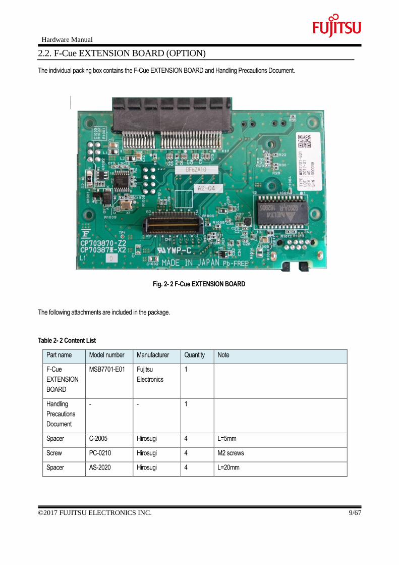
2.2. F-Cue EXTENSION BOARD (OPTION)
The individual packing box contains the F-Cue EXTENSION BOARD and Handling Precautions Document.
Fig. 2- 2 F-Cue EXTENSION BOARD
The following attachments are included in the package.
Table 2- 2 Content List
Part name Model number Manufacturer Quantity Note
F-Cue
EXTENSION
BOARD
MSB7701-E01 Fujitsu
Electronics
1
Handling
Precautions
Document
- - 1
Spacer C-2005 Hirosugi 4 L=5mm
Screw PC-0210 Hirosugi 4 M2 screws
Spacer AS-2020 Hirosugi 4 L=20mm
Hardware Manual
10/67 ©2017 FUJITSU ELECTRONICS INC.
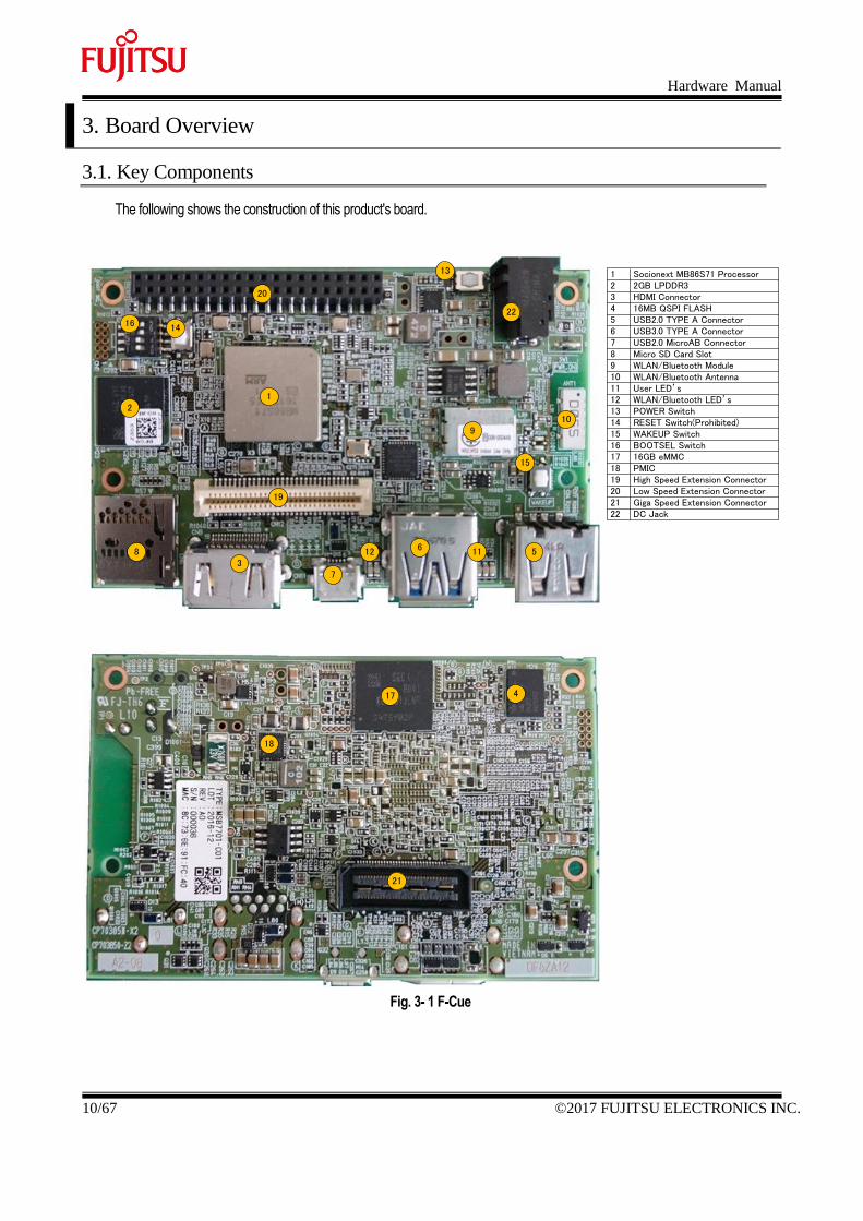
3. Board Overview
3.1. Key Components
The following shows the construction of this product's board.
1 Socionext MB86S71 Processor
High Speed Extension ConnectorLow Speed Extension Connector
Micro SD Card Slot
Giga Speed Extension Connector
WAKEUP SwitchRESET Switch(Prohibited)POWER Switch
PMIC
USB2.0 TYPE A ConnectorUSB3.0 TYPE A ConnectorUSB2.0 MicroAB Connector
2GB LPDDR3
WLAN/Bluetooth Module
HDMI Connector16MB QSPI FLASH
User LED’sWLAN/Bluetooth LED’s
16GB eMMCBOOTSEL Switch
234567891011121314151617181920
WLAN/Bluetooth Antenna
DC Jack2221
12
3
4
56
7
8
910
1112
13
14
15
16
17
18
19
20
21
22
Fig. 3- 1 F-Cue
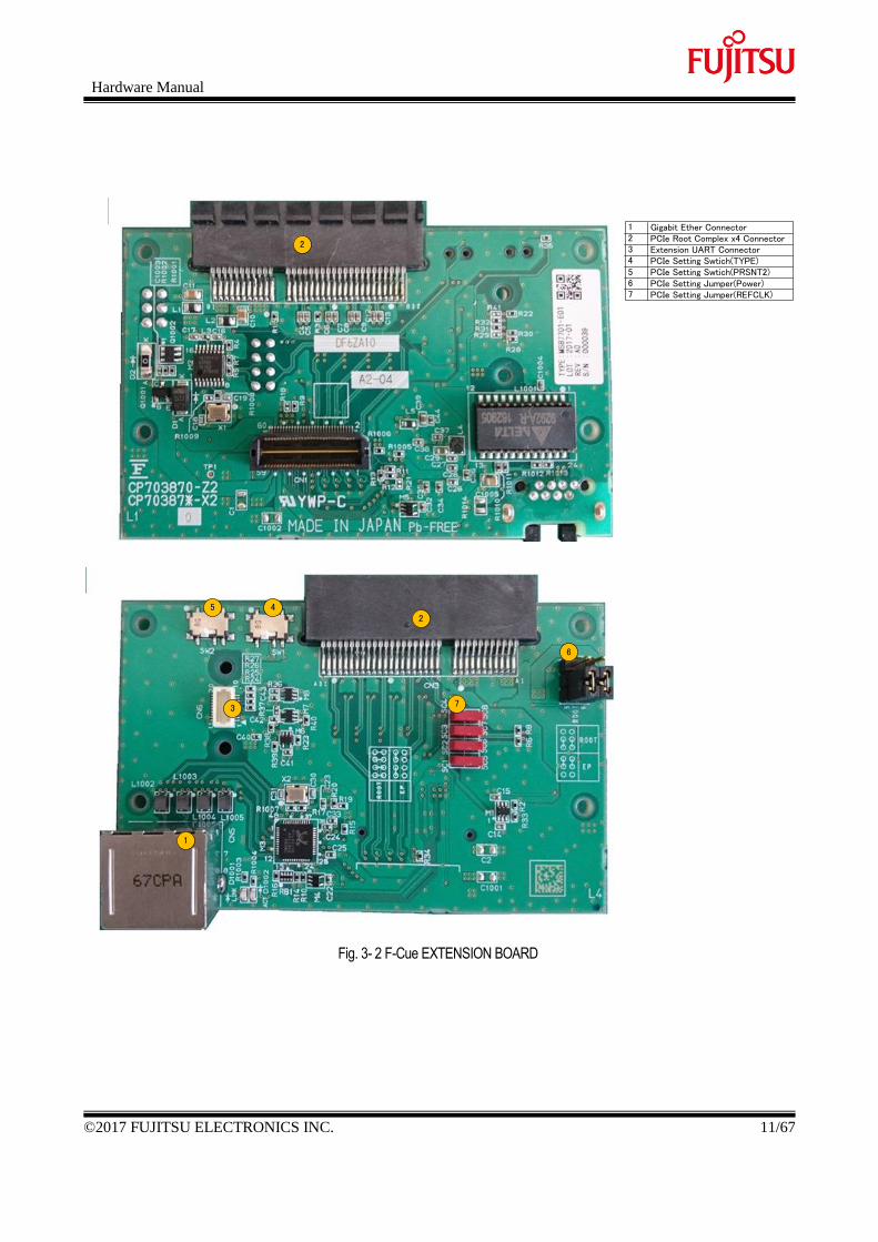
Hardware Manual
©2017 FUJITSU ELECTRONICS INC. 11/67
1
PCIe Setting Swtich(TYPE)
Gigabit Ether Connector234
67
PCIe Root Complex x4 ConnectorExtension UART Connector
PCIe Setting Jumper(Power)PCIe Setting Jumper(REFCLK)
1
2
2
3
4
5 PCIe Setting Swtich(PRSNT2)
5
6
7
Fig. 3- 2 F-Cue EXTENSION BOARD
Hardware Manual
12/67 ©2017 FUJITSU ELECTRONICS INC.
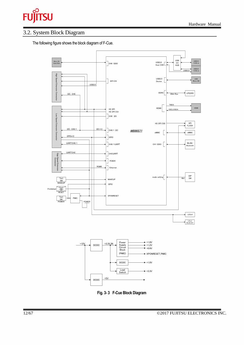
3.2. System Block Diagram
The following figure shows the block diagram of F-Cue.
MB86S71
WAKEUP
I2S
SDIO
I2CI2C×2
GPIO
USB3.0
USB2.0
Device
HS SPI CS1
CH1
USB2.0TYPE A
MIPI-DSI
HDMI
TMDS
DSCL/DSDAHDMI
USB3.0TYPE A
Host CH0
USBMicro AB
USB2.0
SPIFLASH
HS SPI CS0
RGMII
WLAN/Bluetooth
LEDx4
High
Spe
ed E
xtensio
n C
onnecto
rLow
Spe
ed E
xtensio
n C
onnecto
r
GPIOx12
CH0Micro SD
Card Slot SDIO
USB2.0
HUB
DDRC32bit Bus LPDDR3
USB3.0
PCIE#1
Giga S
peed E
xtensio
n
Connecto
r
CH0/1UART
eMMCeMMC
CH0/1UART
CH2UARTCH2UART
CH0
CH0I2C
CH0/1I2CCH0/1
DIPSW
mode setting4bit
HS SPI
TactSW
TactSW
PMIC
RESET
POWER POWER
TactSW
WAKEUP
XPONRESET
GPIO
LEDx2(WLAN/BT)
Prohibited
Ethernet
Power Supply Circuit Block
(PMIC)
+5V
+3.3V_IN
+1.0V
+0.9V
+1.8V
XPONRESET_PMIC
+1.2VDCDC+12V
DCDC
DCDC
+3.3VLoad
Switch
Fig. 3- 3 F-Cue Block Diagram
Hardware Manual
©2017 FUJITSU ELECTRONICS INC. 13/67
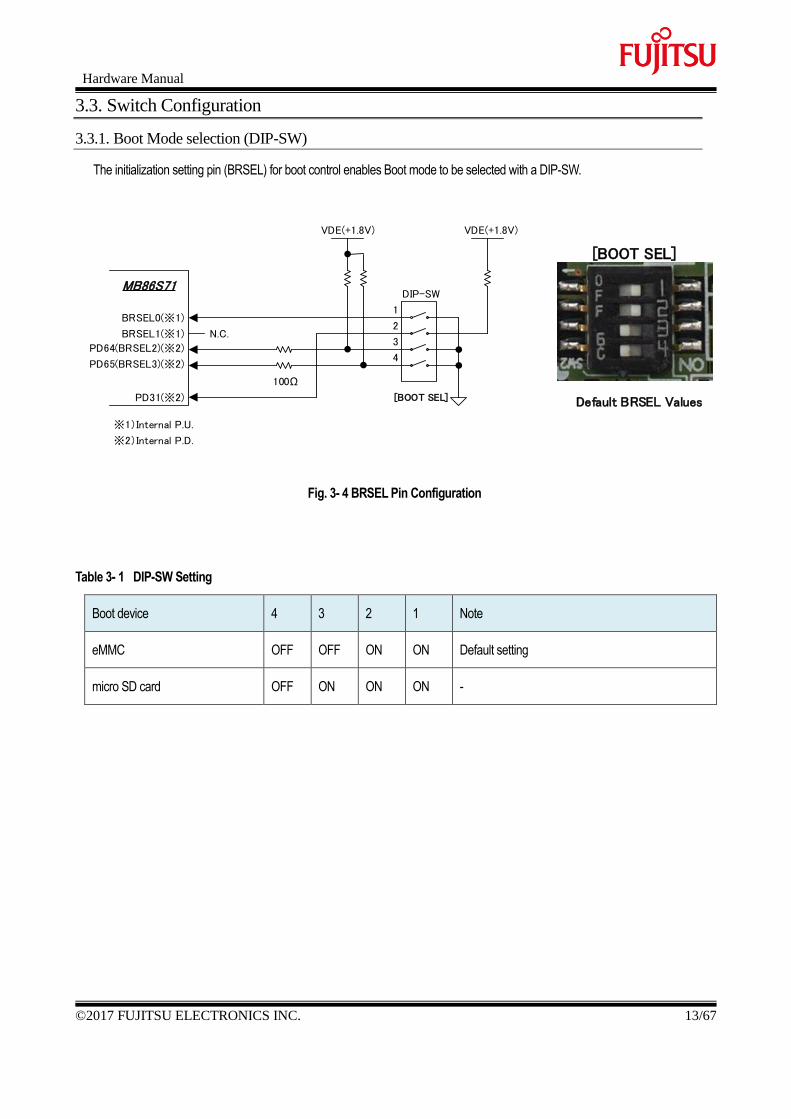
3.3. Switch Configuration
3.3.1. Boot Mode selection (DIP-SW)
The initialization setting pin (BRSEL) for boot control enables Boot mode to be selected with a DIP-SW.
MB86S71
BRSEL0(※1)
DIP-SW
1
2
3
4
BRSEL1(※1)
PD64(BRSEL2)(※2)
PD65(BRSEL3)(※2)
※1)Internal P.U.
※2)Internal P.D.
100Ω
VDE(+1.8V)VDE(+1.8V)
PD31(※2)
N.C.
Default BRSEL Values
[BOOT SEL]
[BOOT SEL]
Fig. 3- 4 BRSEL Pin Configuration
Table 3- 1 DIP-SW Setting
Boot device 4 3 2 1 Note
eMMC OFF OFF ON ON Default setting
micro SD card OFF ON ON ON -
Hardware Manual
14/67 ©2017 FUJITSU ELECTRONICS INC.
4. Getting Started
4.1. Prerequisites
Before powering on F-Cue, you need to prepare the following.
・F-Cue
・AC adapter (The TW-12020U AC adapter and SSCI-025461 converter plug are recommended)
・USB mouse and keyboard
・HDMI monitor and HDMI cable
4.2. Known Limitations
Table 4- 1 Known Limitations
No. Board
REV
Item Description
1 A0 Board reset The Tact-SW reset is not available. A reset using the RST_BTN_N (6-pin) of
the low speed extension connector is available.
2 A0 External WAKEUP input WAKEUP (return from retention mode) with the GPIO-A (23-pin) of the low
speed extension connector is not supported.
3 A0 Automatic power on When power is applied to the DC jack, the board power supply will not turn
on automatically. The board starts after the power switch is pressed.
4 A0 DC jack input range The DC jack does not support a power input range of 8 V to 18 V. Use the
12 V+-5% power.
4.3. First Power ON
The following describes the F-Cue startup procedure.
・Connect F-Cue to the monitor using an HDMI cable.
・Connect the mouse and keyboard to F-Cue.
・Connect the AC adapter to the DC jack and an outlet.
・Press down the power switch.
Hardware Manual
©2017 FUJITSU ELECTRONICS INC. 15/67
5. Component Detail
5.1. Processor
F-Cue has the MB86S71.
Table 5- 1 MB86S71 Details
No. Name Model No. Maker Quantity Remarks
1 MB86S71 MB86S71 socionext 1 Package: FCBGA1183
*Refer to the MB86S71 data sheet.
5.2. PMIC
F-Cue has the PMIC.
Table 5- 2 PMIC Details
No. Name Model No. Maker Quantity Remarks
1 PMIC AS3709-BQFM AMS 1
5.3. Memory/Storage
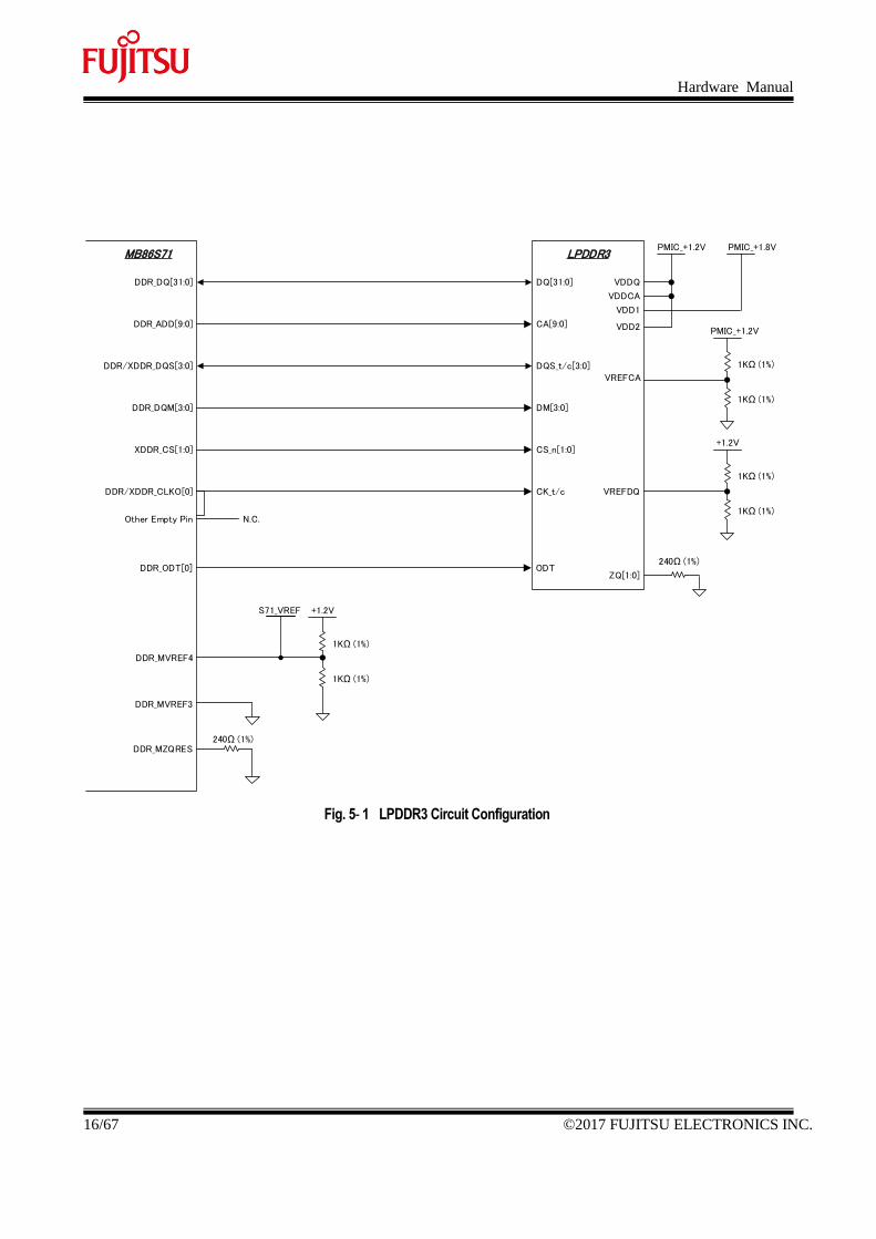
F-Cue has the LPDDR3, eMMC, Micro SD card slot, and HSSPI interface.
5.3.1. LPDDR3
F-Cue has the LPDDR3.
It is Single Channel (x 32bit) compatible and has a data rate of 1333MT/s.
Table 5- 3 LPDDR3 Interface
No. Item Description Remarks
1 Memory capacity 2GB
2 Data rate 1333MT/s
Table 5- 4 LPDDR3 Main Components
No. Function Model No. Maker Quantity Remarks
1 LPDDR3 K4E6E304EB-EGCF Samsung 1 2GB (Single Channel)
Hardware Manual
16/67 ©2017 FUJITSU ELECTRONICS INC.
DDR/XDDR_CLKO[0]
DDR_MVREF4
VREFDQ
MB86S71
DDR_ADD[9:0]
XDDR_CS[1:0]
DDR_DQ[31:0]
DDR_DQM[3:0]
DDR/XDDR_DQS[3:0]
DDR_MZQRES
LPDDR3
DQ[31:0]
CA[9:0]
DQS_t/c[3:0]
DM[3:0]
CS_n[1:0]
ODT
CK_t/c
+1.2V
240Ω (1%)
VREFCA
VDDQ
PMIC_+1.2V PMIC_+1.8V
VDDCA
VDD1
VDD2
Other Empty Pin N.C.
1KΩ (1%)
1KΩ (1%)
ZQ[1:0]
240Ω (1%)
S71_VREF
+1.2V
1KΩ (1%)
1KΩ (1%)
PMIC_+1.2V
1KΩ (1%)
1KΩ (1%)
DDR_MVREF3
DDR_ODT[0]
Fig. 5- 1 LPDDR3 Circuit Configuration
Hardware Manual
©2017 FUJITSU ELECTRONICS INC. 17/67
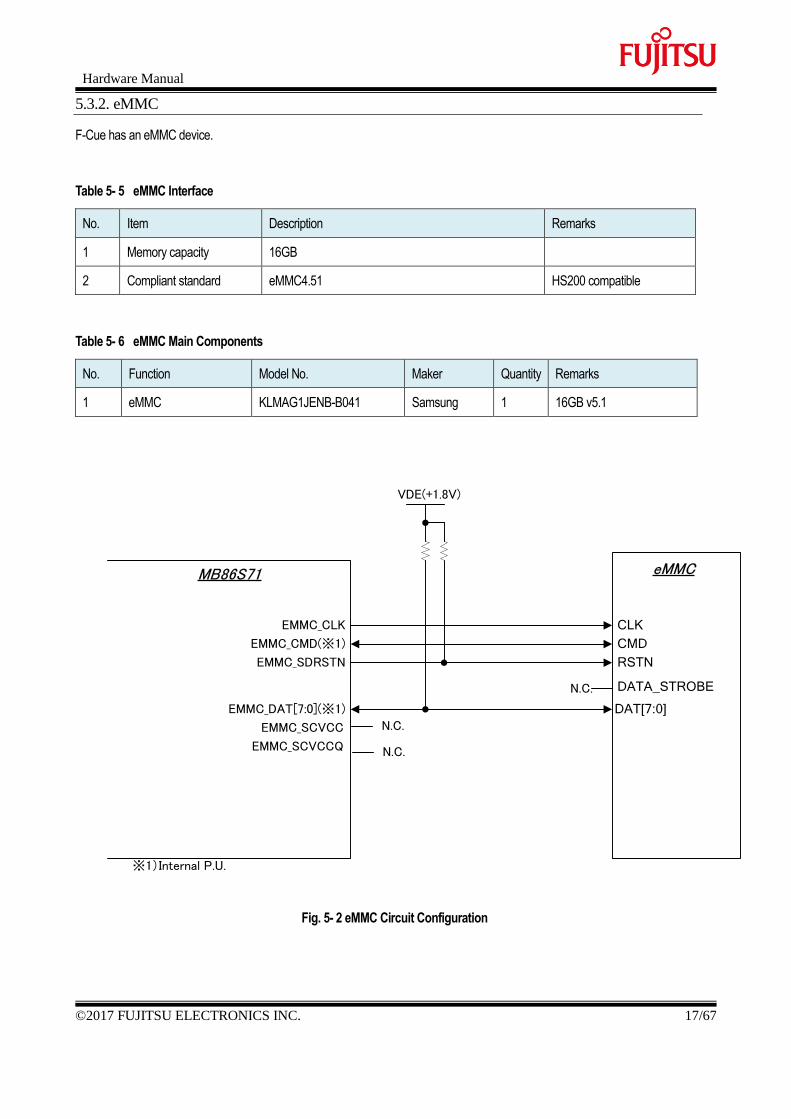
5.3.2. eMMC
F-Cue has an eMMC device.
Table 5- 5 eMMC Interface
No. Item Description Remarks
1 Memory capacity 16GB
2 Compliant standard eMMC4.51 HS200 compatible
Table 5- 6 eMMC Main Components
No. Function Model No. Maker Quantity Remarks
1 eMMC KLMAG1JENB-B041 Samsung 1 16GB v5.1
MB86S71
EMMC_CLK
EMMC_DAT[7:0](※1)
EMMC_SDRSTN
EMMC_SCVCC
※1)Internal P.U.
CLK
eMMC
RSTN
DAT[7:0]
DATA_STROBE
CMDEMMC_CMD(※1)
EMMC_SCVCCQ
VDE(+1.8V)
N.C.
N.C.
N.C.
Fig. 5- 2 eMMC Circuit Configuration
Hardware Manual
18/67 ©2017 FUJITSU ELECTRONICS INC.
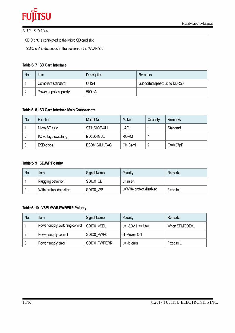
5.3.3. SD Card
SDIO ch0 is connected to the Micro SD card slot.
SDIO ch1 is described in the section on the WLAN/BT.
Table 5- 7 SD Card Interface
No. Item Description Remarks
1 Compliant standard UHS-I Supported speed: up to DDR50
2 Power supply capacity 500mA
Table 5- 8 SD Card Interface Main Components
No. Function Model No. Maker Quantity Remarks
1 Micro SD card ST11S008V4H JAE 1 Standard
2 I/O voltage switching BD2204GUL ROHM 1
3 ESD diode ESD8104MUTAG ON Semi 2 Ct=0.37pF
Table 5- 9 CD/WP Polarity
No. Item Signal Name Polarity Remarks
1 Plugging detection SDIO0_CD L=Insert
2 Write protect detection SDIO0_WP L=Write protect disabled Fixed to L
Table 5- 10 VSEL/PWR/PWRERR Polarity
No. Item Signal Name Polarity Remarks
1 Power supply switching control SDIO0_VSEL L=+3.3V, H=+1.8V When SPMODE=L
2 Power supply control SDIO0_PWR0 H=Power ON
3 Power supply error SDIO0_PWRERR L=No error Fixed to L
Hardware Manual
©2017 FUJITSU ELECTRONICS INC. 19/67
MB86S71
SDIO0_CLK
SDIO0_CMD
SDIO0_PWR0
MicroSD Card Slot
3 CMD
5 CLK
:ESDダイオード
(※1)SDIO0_CD
(※1)SDIO0_WP
SDIO0_VSEL
(※2)SDIO0_PWRERR
VBIASP0
VBIASN0
VBIASPEXT0
VBIASNEXT0
VNODE_N0
2/1/8/7 DAT[3:0]
9 DSW1
11-17 GND
4 PWR
SDIO0_DAT[3:0]
+1.8V
0.22uF
0.22uF
0.22uF
0.22uF
0.22uF
0.22uF
6 GND
※1)Internl P.U.
VDE_SDIO0
+3.3V
VDE_SDIO0
10 DSW2
+3.3V
※2)Internl P.D.
BD2204GUL
EN
VIN2
VIN1
GND
VOUT
SEL
VDE_SDIO0
+3.3V+1.8V
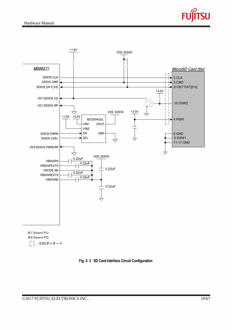
Fig. 5- 3 SD Card Interface Circuit Configuration
Hardware Manual
20/67 ©2017 FUJITSU ELECTRONICS INC.
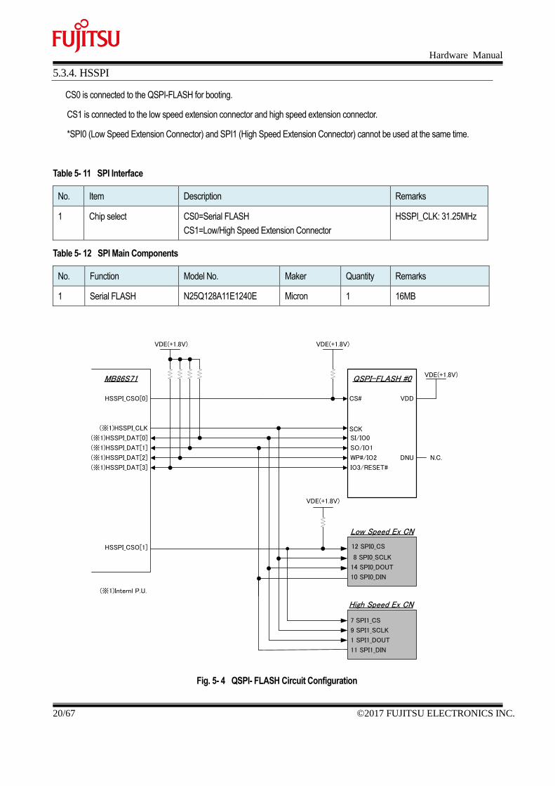
5.3.4. HSSPI
CS0 is connected to the QSPI-FLASH for booting.
CS1 is connected to the low speed extension connector and high speed extension connector.
*SPI0 (Low Speed Extension Connector) and SPI1 (High Speed Extension Connector) cannot be used at the same time.
Table 5- 11 SPI Interface
No. Item Description Remarks
1 Chip select CS0=Serial FLASH
CS1=Low/High Speed Extension Connector
HSSPI_CLK: 31.25MHz
Table 5- 12 SPI Main Components
No. Function Model No. Maker Quantity Remarks
1 Serial FLASH N25Q128A11E1240E Micron 1 16MB
(※1)HSSPI_CLK
CS#
SI/IO0
SCK
QSPI-FLASH #0
N.C.
MB86S71
SO/IO1
WP#/IO2
IO3/RESET#
VDD
DNU
HSSPI_CSO[0]
HSSPI_CSO[1]
(※1)HSSPI_DAT[0]
(※1)HSSPI_DAT[1]
(※1)HSSPI_DAT[2]
(※1)HSSPI_DAT[3]
VDE(+1.8V) VDE(+1.8V)
VDE(+1.8V)
VDE(+1.8V)
Low Speed Ex CN
12 SPI0_CS
8 SPI0_SCLK
10 SPI0_DIN
14 SPI0_DOUT
High Speed Ex CN
7 SPI1_CS
9 SPI1_SCLK
11 SPI1_DIN
1 SPI1_DOUT
(※1)Internl P.U.
Fig. 5- 4 QSPI- FLASH Circuit Configuration
Hardware Manual
©2017 FUJITSU ELECTRONICS INC. 21/67
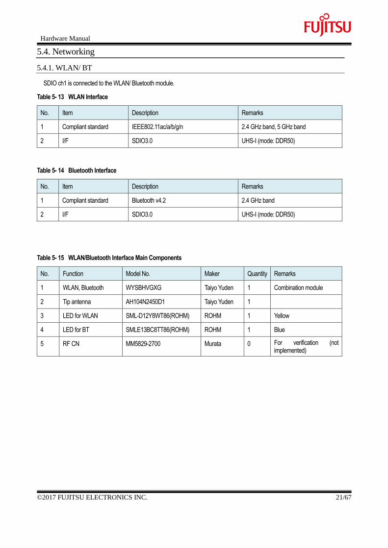
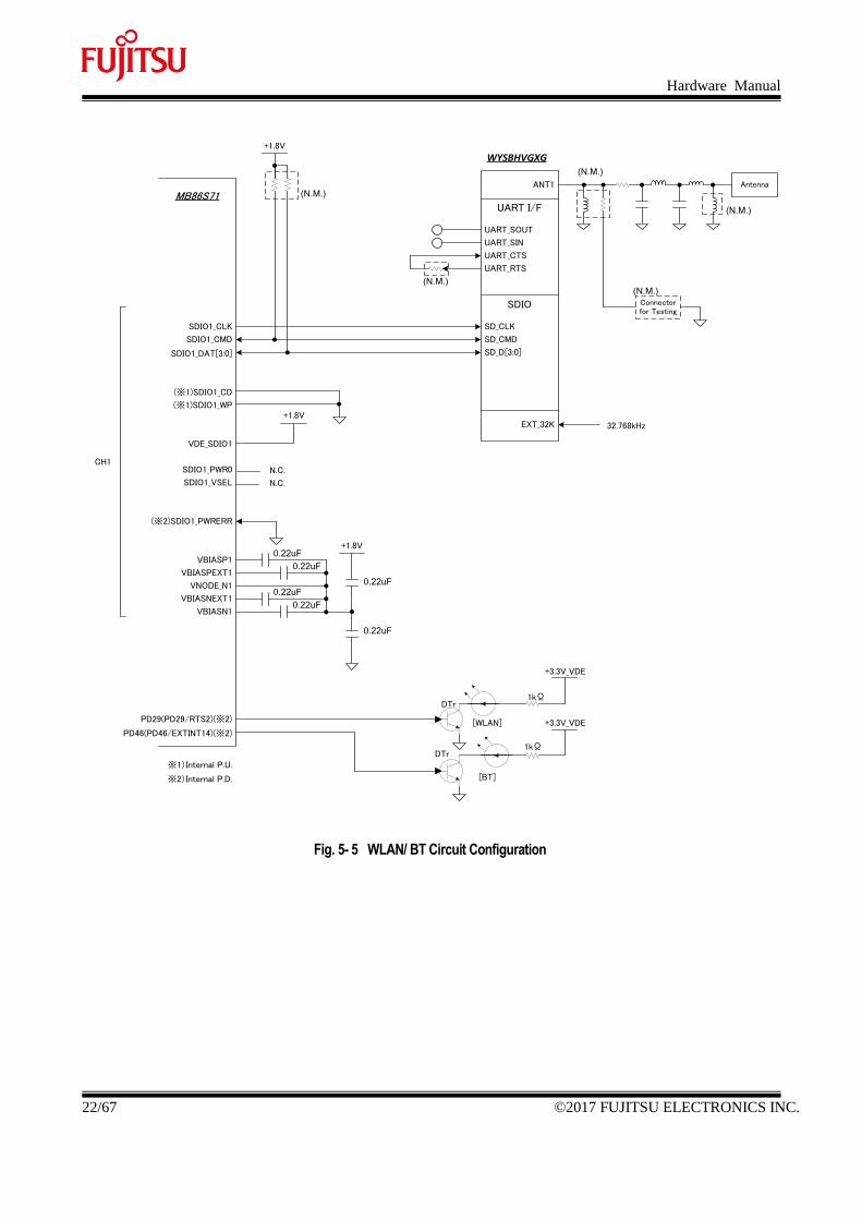
5.4. Networking
5.4.1. WLAN/ BT
SDIO ch1 is connected to the WLAN/ Bluetooth module.
Table 5- 13 WLAN Interface
No. Item Description Remarks
1 Compliant standard IEEE802.11ac/a/b/g/n 2.4 GHz band, 5 GHz band
2 I/F SDIO3.0 UHS-I (mode: DDR50)
Table 5- 14 Bluetooth Interface
No. Item Description Remarks
1 Compliant standard Bluetooth v4.2 2.4 GHz band
2 I/F SDIO3.0 UHS-I (mode: DDR50)
Table 5- 15 WLAN/Bluetooth Interface Main Components
No. Function Model No. Maker Quantity Remarks
1 WLAN, Bluetooth WYSBHVGXG Taiyo Yuden 1 Combination module
2 Tip antenna AH104N2450D1 Taiyo Yuden 1
3 LED for WLAN SML-D12Y8WT86(ROHM) ROHM 1 Yellow
4 LED for BT SMLE13BC8TT86(ROHM) ROHM 1 Blue
5 RF CN MM5829-2700 Murata 0 For verification (not implemented)
Hardware Manual
22/67 ©2017 FUJITSU ELECTRONICS INC.
+1.8V
SDIO1_CLK
SDIO1_CMD
SDIO1_PWR0
(※1)SDIO1_CD
(※1)SDIO1_WP
SDIO1_VSEL
(※2)SDIO1_PWRERR
VBIASP1
VBIASN1
VBIASPEXT1
VBIASNEXT1
VNODE_N1
SDIO1_DAT[3:0]
0.22uF
0.22uF
0.22uF
0.22uF
0.22uF
0.22uF
VDE_SDIO1
WYSBHVGXG
UART_SOUT
MB86S71
UART_SIN
UART_CTS
UART_RTS
+1.8V
UART I/F
SDIO
CH1
SD_CLK
SD_CMD
SD_D[3:0]
+1.8VEXT_32K 32.768kHz
PD29(PD29/RTS2)(※2)
PD46(PD46/EXTINT14)(※2)
DTr1kΩ
+3.3V_VDE
DTr1kΩ
[WLAN]
[BT]※2)Internal P.D.
※1)Internal P.U.
AntennaANT1(N.M.)
(N.M.)
(N.M.)
Connector for Testing
(N.M.)
+3.3V_VDE
N.C.
N.C.
(N.M.)
Fig. 5- 5 WLAN/ BT Circuit Configuration
Hardware Manual
©2017 FUJITSU ELECTRONICS INC. 23/67
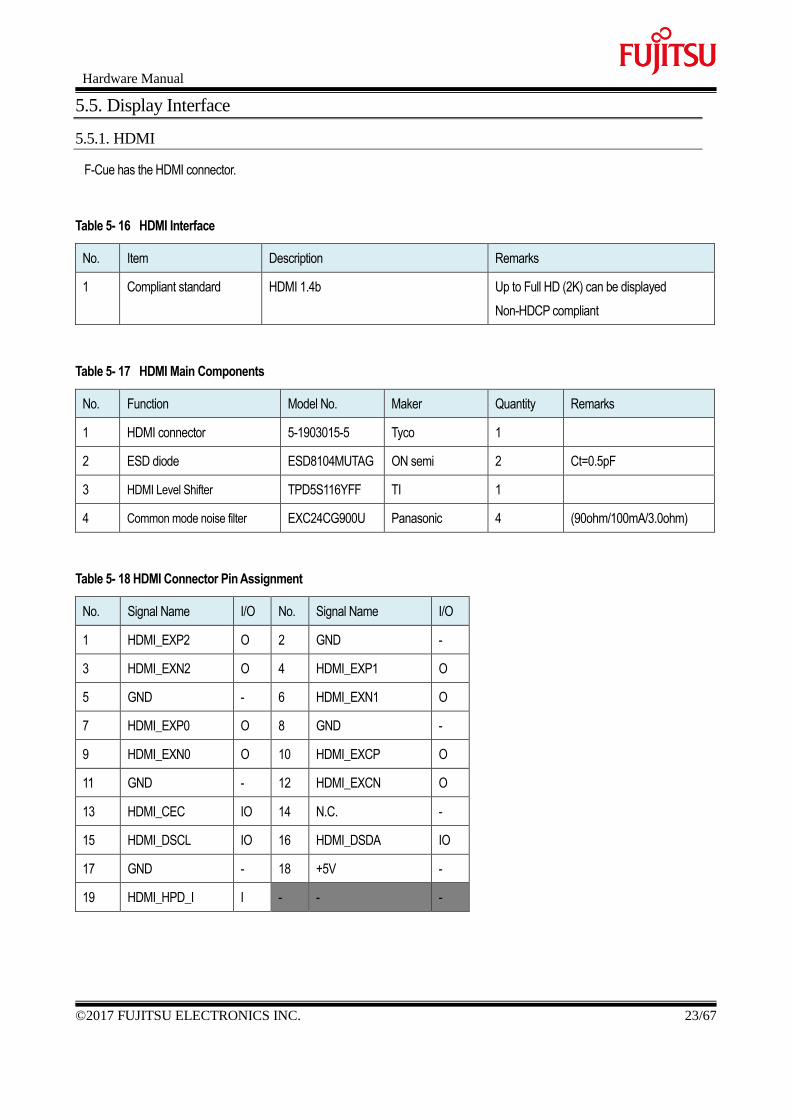
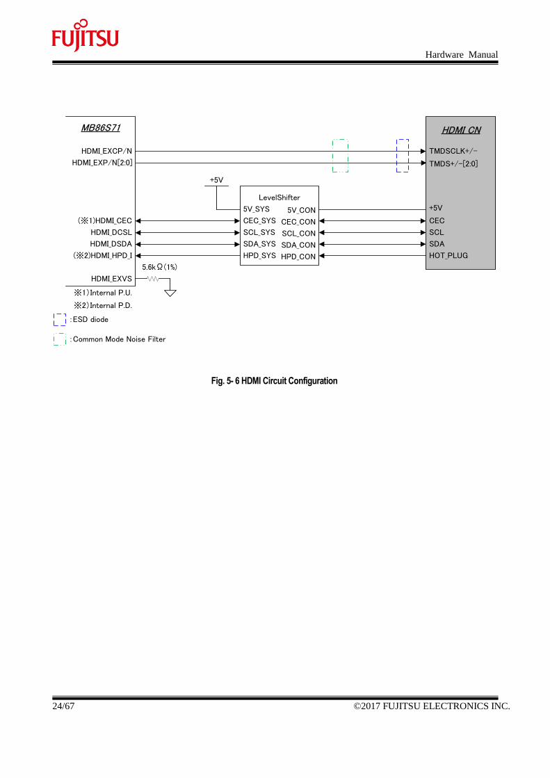
5.5. Display Interface
5.5.1. HDMI
F-Cue has the HDMI connector.
Table 5- 16 HDMI Interface
No. Item Description Remarks
1 Compliant standard HDMI 1.4b Up to Full HD (2K) can be displayed
Non-HDCP compliant
Table 5- 17 HDMI Main Components
No. Function Model No. Maker Quantity Remarks
1 HDMI connector 5-1903015-5 Tyco 1
2 ESD diode ESD8104MUTAG ON semi 2 Ct=0.5pF
3 HDMI Level Shifter TPD5S116YFF TI 1
4 Common mode noise filter EXC24CG900U Panasonic 4 (90ohm/100mA/3.0ohm)
Table 5- 18 HDMI Connector Pin Assignment
No. Signal Name I/O No. Signal Name I/O
1 HDMI_EXP2 O 2 GND -
3 HDMI_EXN2 O 4 HDMI_EXP1 O
5 GND - 6 HDMI_EXN1 O
7 HDMI_EXP0 O 8 GND -
9 HDMI_EXN0 O 10 HDMI_EXCP O
11 GND - 12 HDMI_EXCN O
13 HDMI_CEC IO 14 N.C. -
15 HDMI_DSCL IO 16 HDMI_DSDA IO
17 GND - 18 +5V -
19 HDMI_HPD_I I - - -
Hardware Manual
24/67 ©2017 FUJITSU ELECTRONICS INC.
MB86S71
HDMI_EXCP/N
HDMI_EXP/N[2:0]
HDMI_EXVS
(※1)HDMI_CEC
HDMI_DCSL
HDMI_DSDA
(※2)HDMI_HPD_I
HDMI CN
TMDS+/-[2:0]
TMDSCLK+/-
:ESD diode
LevelShifter
CEC_SYS
SCL_SYS
SDA_SYS
HPD_SYS
5V_SYS
+5V
CEC_CON
SCL_CON
SDA_CON
HPD_CON
5V_CON
CEC
SCL
SDA
HOT_PLUG
5.6kΩ(1%)
+5V
:Common Mode Noise Filter
※2)Internal P.D.
※1)Internal P.U.
Fig. 5- 6 HDMI Circuit Configuration
Hardware Manual
©2017 FUJITSU ELECTRONICS INC. 25/67
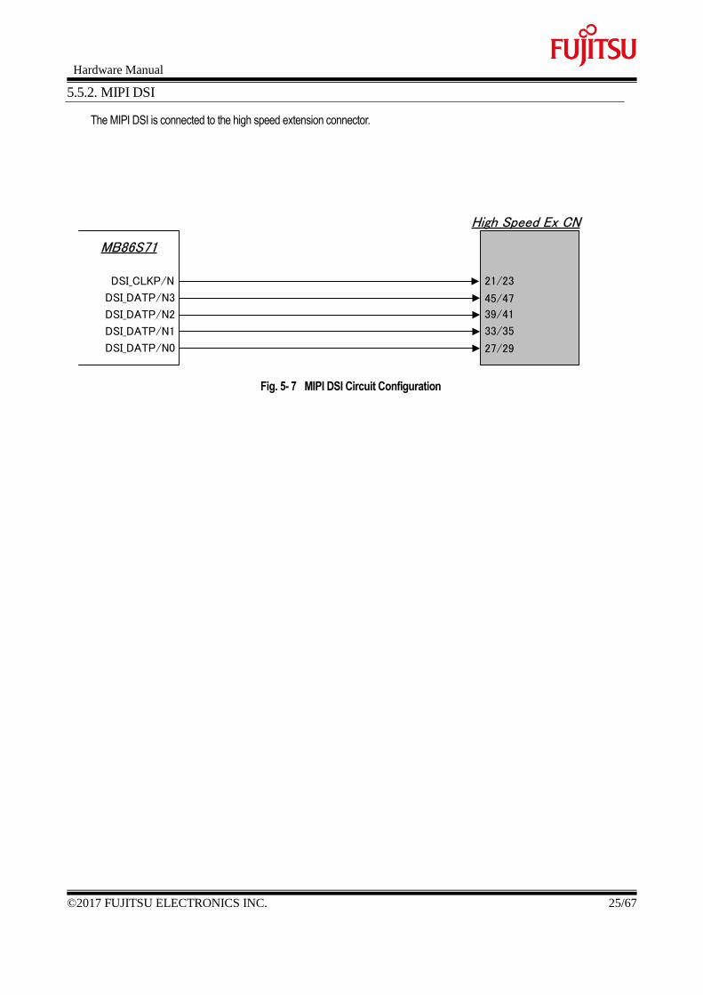
5.5.2. MIPI DSI
The MIPI DSI is connected to the high speed extension connector.
MB86S71
DSI_CLKP/N
DSI_DATP/N3 45/47
21/23
High Speed Ex CN
DSI_DATP/N2
DSI_DATP/N1
DSI_DATP/N0
39/41
33/35
27/29
Fig. 5- 7 MIPI DSI Circuit Configuration
Hardware Manual
26/67 ©2017 FUJITSU ELECTRONICS INC.
5.6. USB Ports
F-Cue has 4 USB ports.
Table 5- 19 USB Ports
No. Item Function Remarks
1 USB3.0 Type-A Host
2 USB2.0 Type-A Host
3 High Speed Ex CN Host
4 USB2.0 Micro-AB Device
5.6.1. USB3.0/2.0 Host
F-Cue has 1 USB3.0 host port and 2 USB2.0 host ports.
Table 5- 20 USB3.0/2.0 Host Interface
No. Item Connector Remarks
1 USB3.0 Host USB3.0 Type-A VBUS power supply capacity: 900mA MAX
2 USB2.0 Host USB2.0 Type-A VBUS power supply capacity: 500mA MAX
High Speed Ex CN VBUS power supply capacity: -
Table 5- 21 USB3.0/2.0 Host Main Components
No. Function Model No. Maker Quantity Remarks
1 USB3.0 Type-A PC2RN1SU41B09S1 JAE 1
2 USB2.0 Type-A UB51123-SH1-4F Foxconn 1
3 USB HUB USB2514B-AEZG SMSC 1
4 High Side Switch MIC2098-1YMT MICREL 1
5 High Side Switch MIC2026-1YM MICREL 1 Dual-Channel
6 Crystal oscillator NZ2520SD-20.000000M-NSA3446E NDK 1 20MHz+-50ppm
7 1Gate Inverter SN74AUP1G00DCKR TI 1 Schmidt
8 ESD diode ESD8104MUTAG ON Semi 3 Ct=0.37pF
9 Common mode
noise filter EXC24CG900U Panasonic 4 90ohm/100mA/3.0ohm
Hardware Manual
©2017 FUJITSU ELECTRONICS INC. 27/67
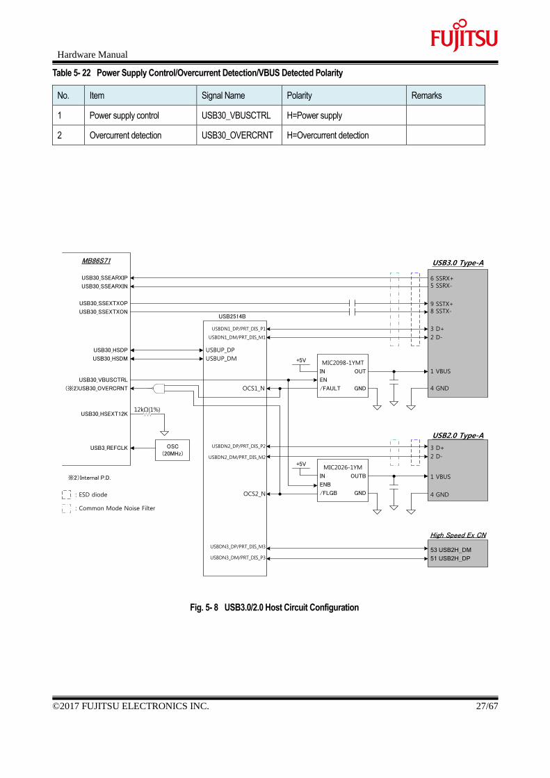
Table 5- 22 Power Supply Control/Overcurrent Detection/VBUS Detected Polarity
No. Item Signal Name Polarity Remarks
1 Power supply control USB30_VBUSCTRL H=Power supply
2 Overcurrent detection USB30_OVERCRNT H=Overcurrent detection
MB86S71
USB30_SSEARXIP
※2)Internal P.D.
USB30_SSEXTXOP
USB30_HSDP
USB30_SSEARXIN
USB30_SSEXTXON
USB30_HSDM
USB30_VBUSCTRL
(※2)USB30_OVERCRNT
USB3_REFCLK
USB30_HSEXT12K
1 VBUS
USB3.0 Type-A
2 D-
3 D+
4 GND
12kΩ(1%)
:ESD diode
OSC(20MHz)
MIC2098-1YMT
/FAULT
EN
IN
GND
OUT
+5V
USB2.0 Type-A
1 VBUS
2 D-
3 D+
4 GND
6 SSRX+5 SSRX-
9 SSTX+8 SSTX-
High Speed Ex CN
51 USB2H_DP
53 USB2H_DM
USB2514B
MIC2026-1YM
/FLGB
ENB
IN
GND
OUTB
+5V
:Common Mode Noise Filter
USBUP_DP
USBUP_DM
USBDN1_DP/PRT_DIS_P1
USBDN1_DM/PRT_DIS_M1
OCS1_N
USBDN2_DP/PRT_DIS_P2
USBDN2_DM/PRT_DIS_M2
OCS2_N
USBDN3_DP/PRT_DIS_M3
USBDN3_DM/PRT_DIS_P3
Fig. 5- 8 USB3.0/2.0 Host Circuit Configuration
Hardware Manual
28/67 ©2017 FUJITSU ELECTRONICS INC.
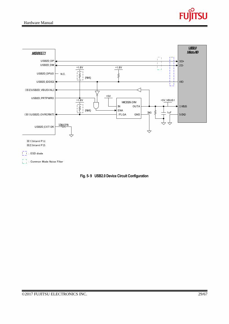
5.6.2. USB2.0 Device
F-Cue has 1 USB2.0 device port.
Table 5- 23 USB2.0 Device Interface
No. Item Connector Remarks
1 USB2.0 Device USB2.0 Micro-AB Only devices are supported
Table 5- 24 USB2.0 Device Main Components
No. Function Model No. Maker Quantity Remarks
1 Micro-AB CN ZX62D-AB-5P8 HRS 1
2 High Side Switch MIC2026-1YM MICREL 1 Dual-Channel
3 1Gate Inverter TC7SZ14FU Toshiba 1 Schmidt
4 1Gate Buffer NL17SZ17XV5 ON Semi 1 Schmidt
5 1Gate AND TC7SZ08FE Toshiba 1
6 ESD diode ESD8104MUTAG ON semi 2 Ct=0.37pF
7 Common mode noise
filter
DLW21HN900HQ2# Murata Manufacturing Co., Ltd.
1 90ohm/220mA/0.59ohm
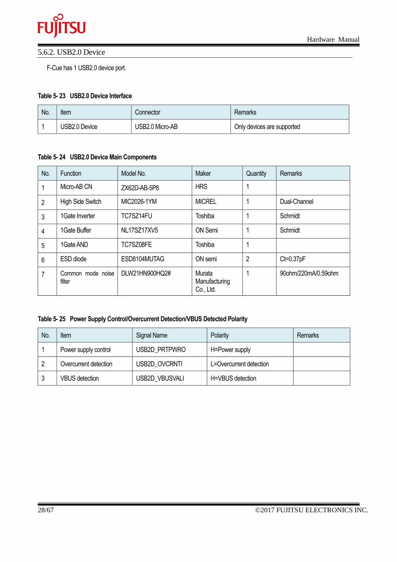
Table 5- 25 Power Supply Control/Overcurrent Detection/VBUS Detected Polarity
No. Item Signal Name Polarity Remarks
1 Power supply control USB2D_PRTPWRO H=Power supply
2 Overcurrent detection USB2D_OVCRNTI L=Overcurrent detection
3 VBUS detection USB2D_VBUSVALI H=VBUS detection
Hardware Manual
©2017 FUJITSU ELECTRONICS INC. 29/67
MB86S71
USB2D_DP
USB2D_DM
USB2D_PRTPWRO
(※1)USB2D_OVRCRNTI
USB2D_EXT12K
1 VBUS
USB2.0
Micro-AB
2 D-
3 D+
5 GND
+5V
12kΩ(1%)
+1.8V
:ESD diode
4 ID
USB2D_DPUO
USB2D_IDDIGI
※1)Internl P.U.
(N.M.)
(※2)USB2D_VBUSVALI
※2)Internl P.D.
1kΩ 1uF
N.C.
MIC2026-1YM
/FLGA
ENA
IN
GND
OUTA
:Common Mode Noise Filter
+1.8V +1.8V
(N.M.)
+5V_VBUS1
Fig. 5- 9 USB2.0 Device Circuit Configuration
Hardware Manual
30/67 ©2017 FUJITSU ELECTRONICS INC.
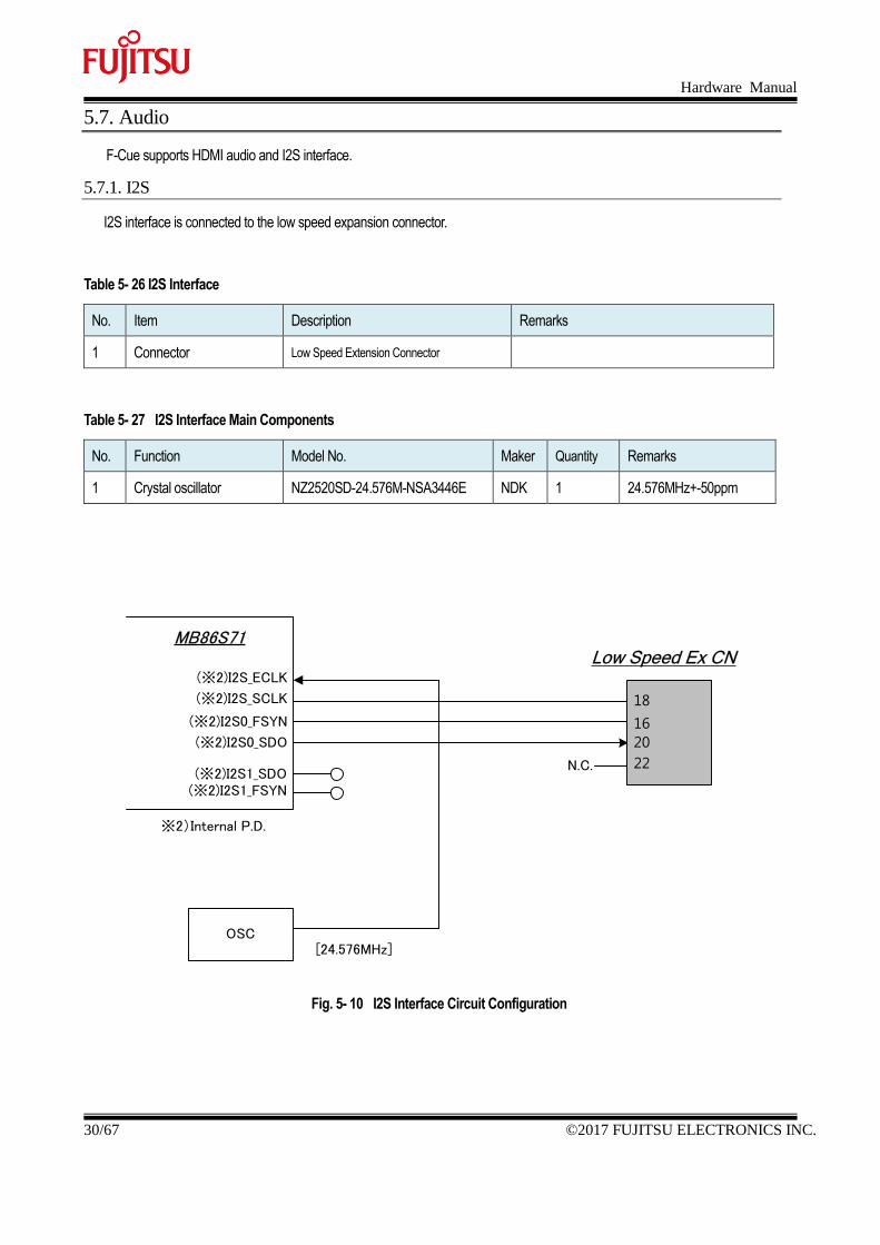
5.7. Audio
F-Cue supports HDMI audio and I2S interface.
5.7.1. I2S
I2S interface is connected to the low speed expansion connector.
Table 5- 26 I2S Interface
No. Item Description Remarks
1 Connector Low Speed Extension Connector
Table 5- 27 I2S Interface Main Components
No. Function Model No. Maker Quantity Remarks
1 Crystal oscillator NZ2520SD-24.576M-NSA3446E NDK 1 24.576MHz+-50ppm
MB86S71
(※2)I2S_ECLK
(※2)I2S_SCLK
(※2)I2S1_SDO
※2)Internal P.D.
(※2)I2S0_FSYN
OSC
18
16
20
[24.576MHz]
Low Speed Ex CN
22
(※2)I2S0_SDO
(※2)I2S1_FSYN
N.C.
Fig. 5- 10 I2S Interface Circuit Configuration
Hardware Manual
©2017 FUJITSU ELECTRONICS INC. 31/67
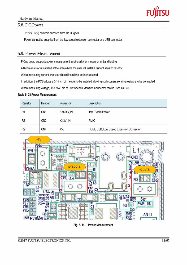
5.8. DC Power
+12V (+-5%) power is supplied from the DC jack.
Power cannot be supplied from the low speed extension connector or a USB connector.
5.9. Power Measurement
F-Cue board supports power measurement functionality for measurement and testing.
A 0-ohm resistor is installed at the area where the user will install a current sensing resistor.
When measuring current, the user should install the resistor required.
In addition, the PCB allows a 0.1-inch pin header to be installed allowing such current sensing resistors to be connected.
When measuring voltage, 1/2/39/49 pin of Low Speed Extension Connector can be used as GND.
Table 5- 28 Power Measurement
Resistor Header Power Rail Description
R1 CN1 SYSDC_IN Total Board Power
R3 CN2 +3.3V_IN PMIC
R9 CN4 +5V HDMI, USB, Low Speed Extension Connector
SYSDC_IN
+5V
+3.3V_IN
Fig. 5- 11 Power Measurement
Hardware Manual
32/67 ©2017 FUJITSU ELECTRONICS INC.
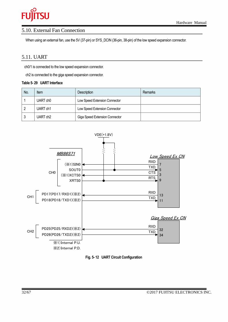
5.10. External Fan Connection
When using an external fan, use the 5V (37-pin) or SYS_DCIN (36-pin, 38-pin) of the low speed expansion connector.
5.11. UART
ch0/1 is connected to the low speed expansion connector.
ch2 is connected to the giga speed expansion connector.
Table 5- 29 UART Interface
No. Item Description Remarks
1 UART ch0 Low Speed Extension Connector
2 UART ch1 Low Speed Extension Connector
3 UART ch2 Giga Speed Extension Connector
(※1)XCTS0
MB86S71
SOUT0
(※1)SIN0
XRTS0RTS
CTS
RXD
TXD
VDE(+1.8V)
3
9
7
CH05
Low Speed Ex CN
※1)Internal P.U.
CH1RXD
TXD13
11
PD17(PD17/RXD1)(※2)
PD18(PD18/TXD1)(※2)
※2)Internal P.D.
Giga Speed Ex CN
32
34
RXD
TXDCH2PD25(PD25/RXD2)(※2)
PD26(PD26/TXD2)(※2)
Fig. 5- 12 UART Circuit Configuration
Hardware Manual
©2017 FUJITSU ELECTRONICS INC. 33/67
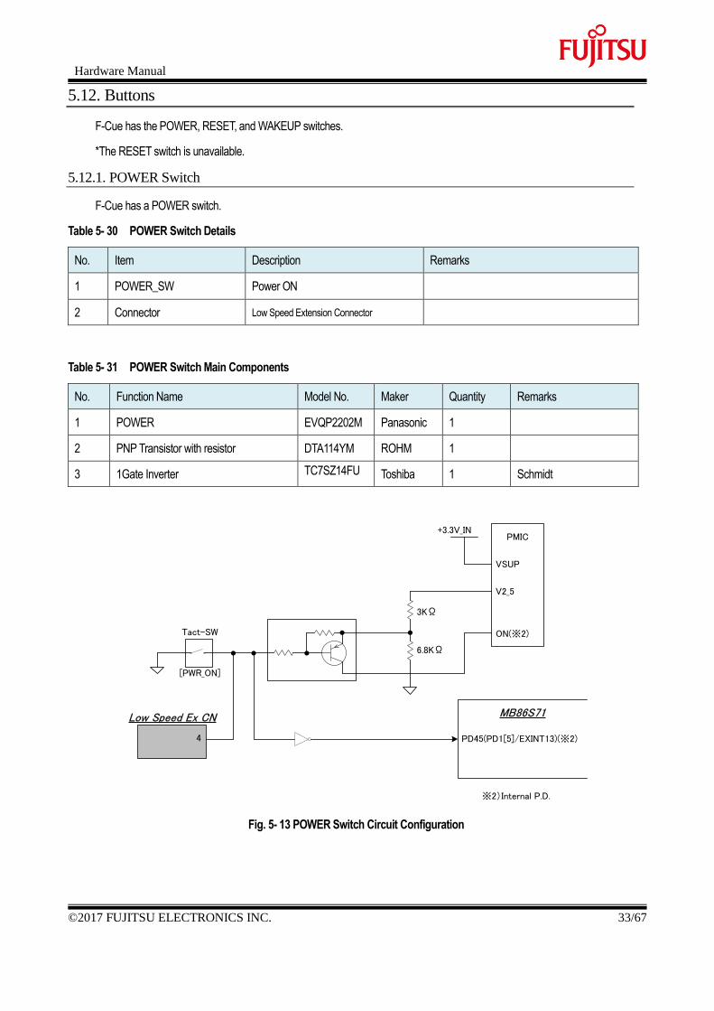
5.12. Buttons
F-Cue has the POWER, RESET, and WAKEUP switches.
*The RESET switch is unavailable.
5.12.1. POWER Switch
F-Cue has a POWER switch.
Table 5- 30 POWER Switch Details
No. Item Description Remarks
1 POWER_SW Power ON
2 Connector Low Speed Extension Connector
Table 5- 31 POWER Switch Main Components
No. Function Name Model No. Maker Quantity Remarks
1 POWER EVQP2202M Panasonic 1
2 PNP Transistor with resistor DTA114YM ROHM 1
3 1Gate Inverter TC7SZ14FU Toshiba 1 Schmidt
※2)Internal P.D.
+3.3V_IN
Tact-SW
[PWR_ON]
Low Speed Ex CN
4
PMIC
VSUP
V2_5
ON(※2)
3KΩ
6.8KΩ
MB86S71
PD45(PD1[5]/EXINT13)(※2)
Fig. 5- 13 POWER Switch Circuit Configuration
Hardware Manual
34/67 ©2017 FUJITSU ELECTRONICS INC.
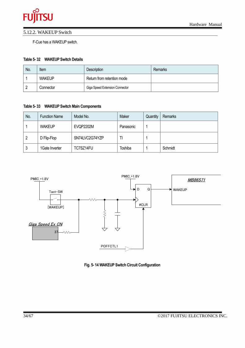
5.12.2. WAKEUP Switch
F-Cue has a WAKEUP switch.
Table 5- 32 WAKEUP Switch Details
No. Item Description Remarks
1 WAKEUP Return from retention mode
2 Connector Giga Speed Extension Connector
Table 5- 33 WAKEUP Switch Main Components
No. Function Name Model No. Maker Quantity Remarks
1 WAKEUP EVQP2202M Panasonic 1
2 D Flip-Flop SN74LVC2G74YZP TI 1
3 1Gate Inverter TC7SZ14FU Toshiba 1 Schmidt
Tact-SW
[WAKEUP]
Giga Speed Ex CN
37
MB86S71
WAKEUP
PMIC_+1.8VPMIC_+1.8V
D Q
#CLR
POFFCTL1
Fig. 5- 14 WAKEUP Switch Circuit Configuration
Hardware Manual
©2017 FUJITSU ELECTRONICS INC. 35/67
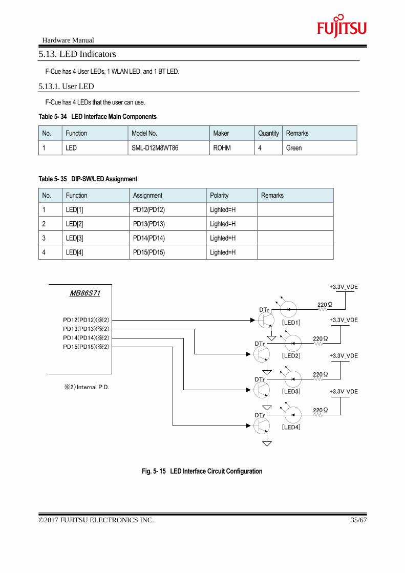
5.13. LED Indicators
F-Cue has 4 User LEDs, 1 WLAN LED, and 1 BT LED.
5.13.1. User LED
F-Cue has 4 LEDs that the user can use.
Table 5- 34 LED Interface Main Components
No. Function Model No. Maker Quantity Remarks
1 LED SML-D12M8WT86 ROHM 4 Green
Table 5- 35 DIP-SW/LED Assignment
No. Function Assignment Polarity Remarks
1 LED[1] PD12(PD12) Lighted=H
2 LED[2] PD13(PD13) Lighted=H
3 LED[3] PD14(PD14) Lighted=H
4 LED[4] PD15(PD15) Lighted=H
MB86S71
PD12(PD12)(※2)
DTr220Ω
+3.3V_VDE
DTr220Ω
DTr220Ω
DTr220Ω
[LED1]
[LED2]
[LED3]
[LED4]
PD13(PD13)(※2)
PD14(PD14)(※2)
PD15(PD15)(※2)
※2)Internal P.D.
+3.3V_VDE
+3.3V_VDE
+3.3V_VDE
Fig. 5- 15 LED Interface Circuit Configuration
Hardware Manual
36/67 ©2017 FUJITSU ELECTRONICS INC.
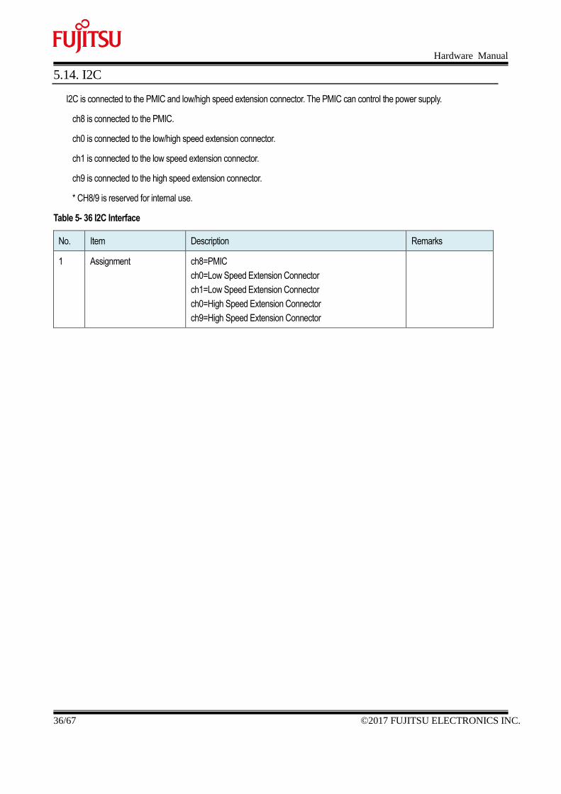
5.14. I2C
I2C is connected to the PMIC and low/high speed extension connector. The PMIC can control the power supply.
ch8 is connected to the PMIC.
ch0 is connected to the low/high speed extension connector.
ch1 is connected to the low speed extension connector.
ch9 is connected to the high speed extension connector.
* CH8/9 is reserved for internal use.
Table 5- 36 I2C Interface
No. Item Description Remarks
1 Assignment ch8=PMIC
ch0=Low Speed Extension Connector
ch1=Low Speed Extension Connector
ch0=High Speed Extension Connector
ch9=High Speed Extension Connector
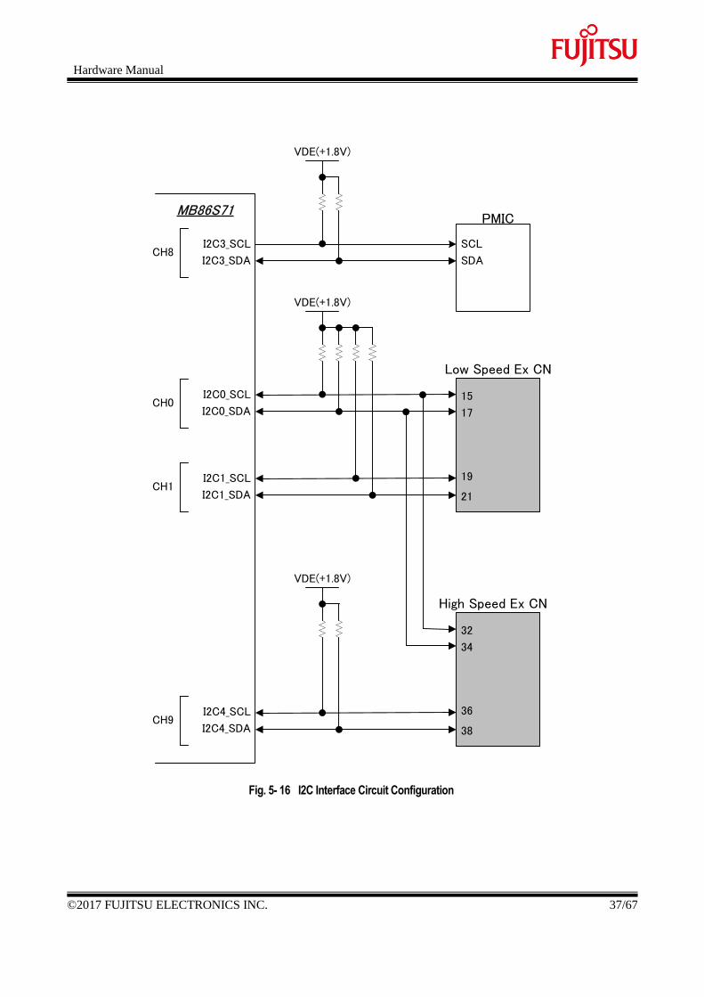
Hardware Manual
©2017 FUJITSU ELECTRONICS INC. 37/67
I2C0_SDA
VDE(+1.8V)
I2C0_SCLCH0
Low Speed Ex CN
15
17
19
21
VDE(+1.8V)
High Speed Ex CN
32
34
36
38I2C4_SDA
I2C4_SCLCH9
I2C1_SDA
I2C1_SCLCH1
MB86S71
I2C3_SCL
VDE(+1.8V)
CH8I2C3_SDA
PMIC
SCL
SDA
Fig. 5- 16 I2C Interface Circuit Configuration
Hardware Manual
38/67 ©2017 FUJITSU ELECTRONICS INC.
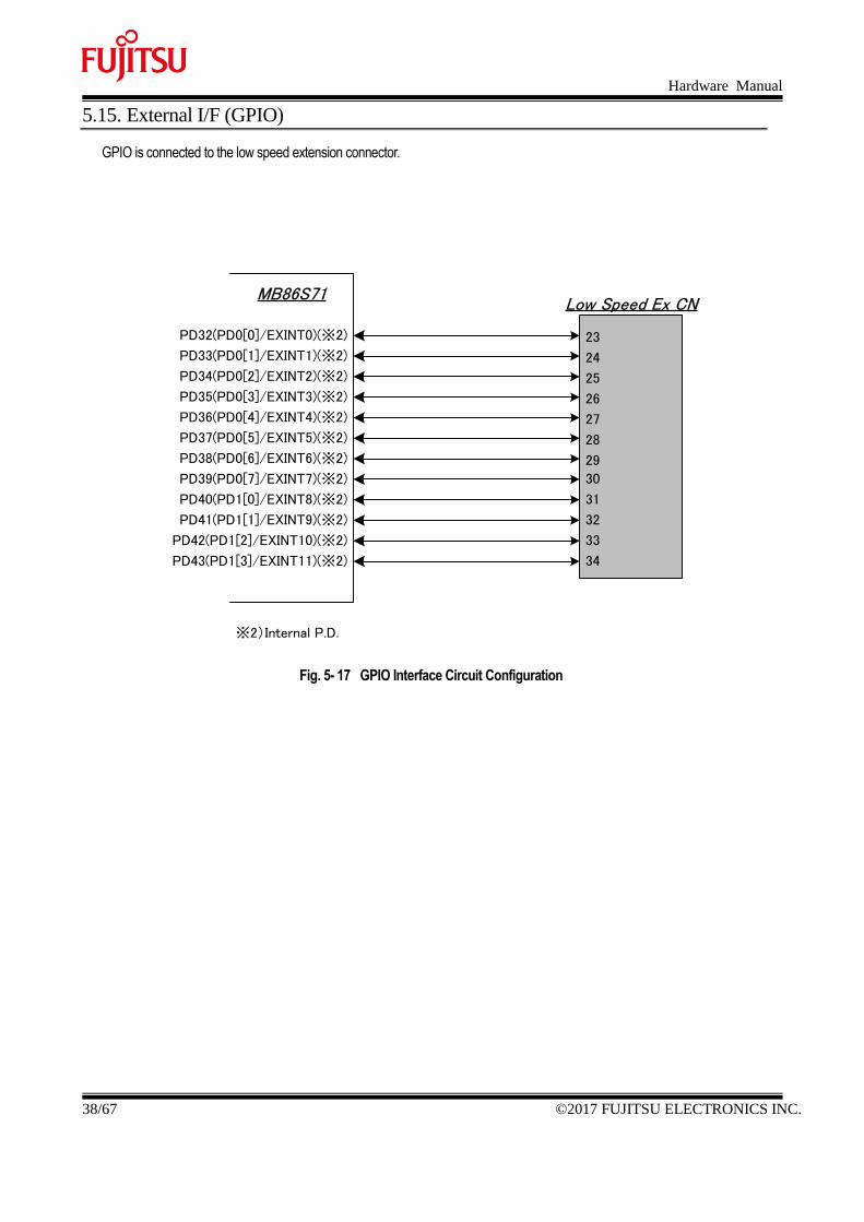
5.15. External I/F (GPIO)
GPIO is connected to the low speed extension connector.
MB86S71
PD36(PD0[4]/EXINT4)(※2)
PD37(PD0[5]/EXINT5)(※2)
PD35(PD0[3]/EXINT3)(※2)
PD34(PD0[2]/EXINT2)(※2)
PD33(PD0[1]/EXINT1)(※2)
PD32(PD0[0]/EXINT0)(※2)
PD38(PD0[6]/EXINT6)(※2)
PD39(PD0[7]/EXINT7)(※2)
PD40(PD1[0]/EXINT8)(※2)
PD41(PD1[1]/EXINT9)(※2)
PD42(PD1[2]/EXINT10)(※2)
PD43(PD1[3]/EXINT11)(※2)
※2)Internal P.D.
Low Speed Ex CN
23
24
28
29
25
26
27
30
31
32
33
34
Fig. 5- 17 GPIO Interface Circuit Configuration
Hardware Manual
©2017 FUJITSU ELECTRONICS INC. 39/67
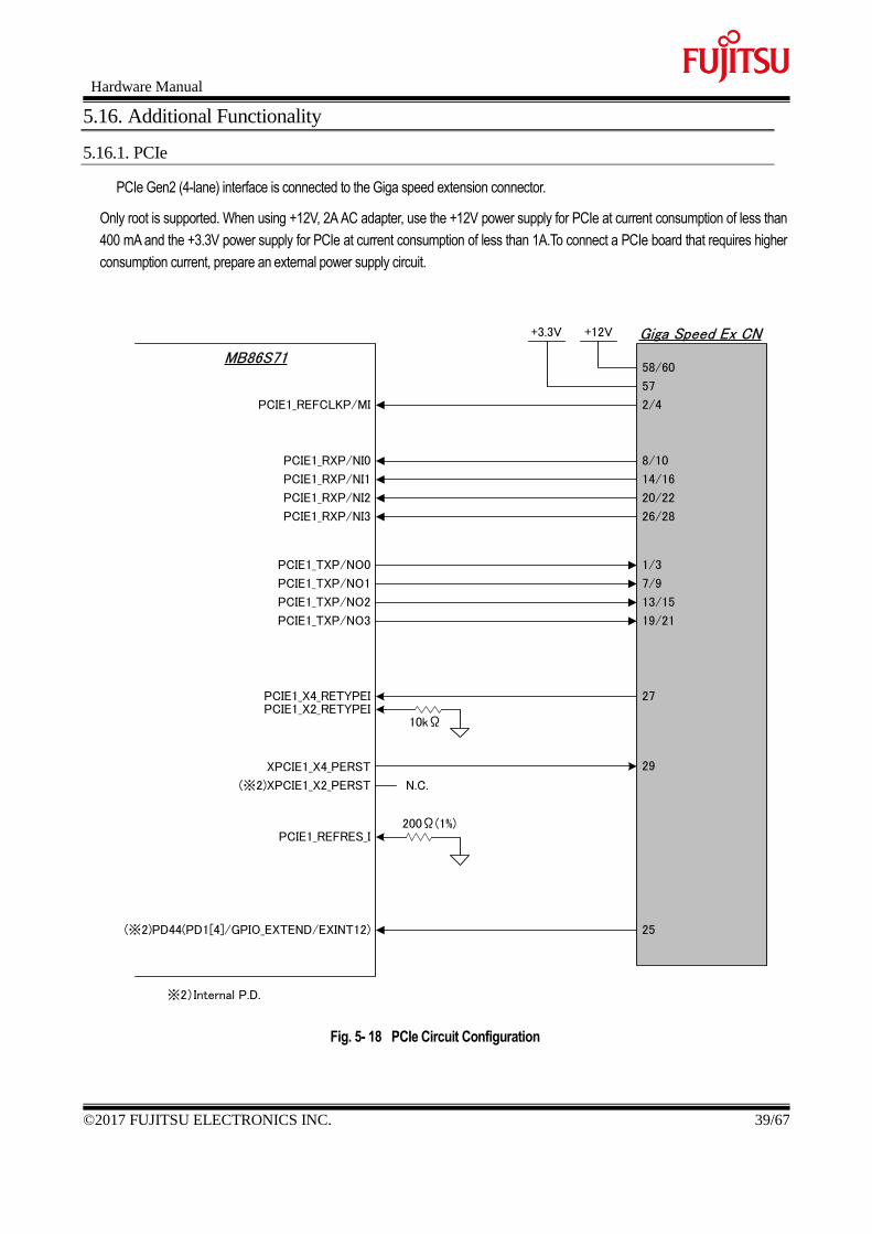
5.16. Additional Functionality
5.16.1. PCIe
PCIe Gen2 (4-lane) interface is connected to the Giga speed extension connector.
Only root is supported. When using +12V, 2A AC adapter, use the +12V power supply for PCIe at current consumption of less than
400 mA and the +3.3V power supply for PCIe at current consumption of less than 1A.To connect a PCIe board that requires higher
consumption current, prepare an external power supply circuit.
MB86S71
PCIE1_REFCLKP/MI
PCIE1_RXP/NI0
PCIE1_TXP/NO0
PCIE1_X2_RETYPEIPCIE1_X4_RETYPEI
(※2)XPCIE1_X2_PERST
XPCIE1_X4_PERST
PCIE1_REFRES_I200Ω(1%)
10kΩ
PCIE1_RXP/NI1
PCIE1_RXP/NI2
PCIE1_RXP/NI3
PCIE1_TXP/NO1
PCIE1_TXP/NO2
PCIE1_TXP/NO3
※2)Internal P.D.
2/4
27
29
25
Giga Speed Ex CN
8/10
14/16
20/22
26/28
1/3
7/9
13/15
19/21
(※2)PD44(PD1[4]/GPIO_EXTEND/EXINT12)
N.C.
+12V
58/60
+3.3V
57
Fig. 5- 18 PCIe Circuit Configuration
Hardware Manual
40/67 ©2017 FUJITSU ELECTRONICS INC.
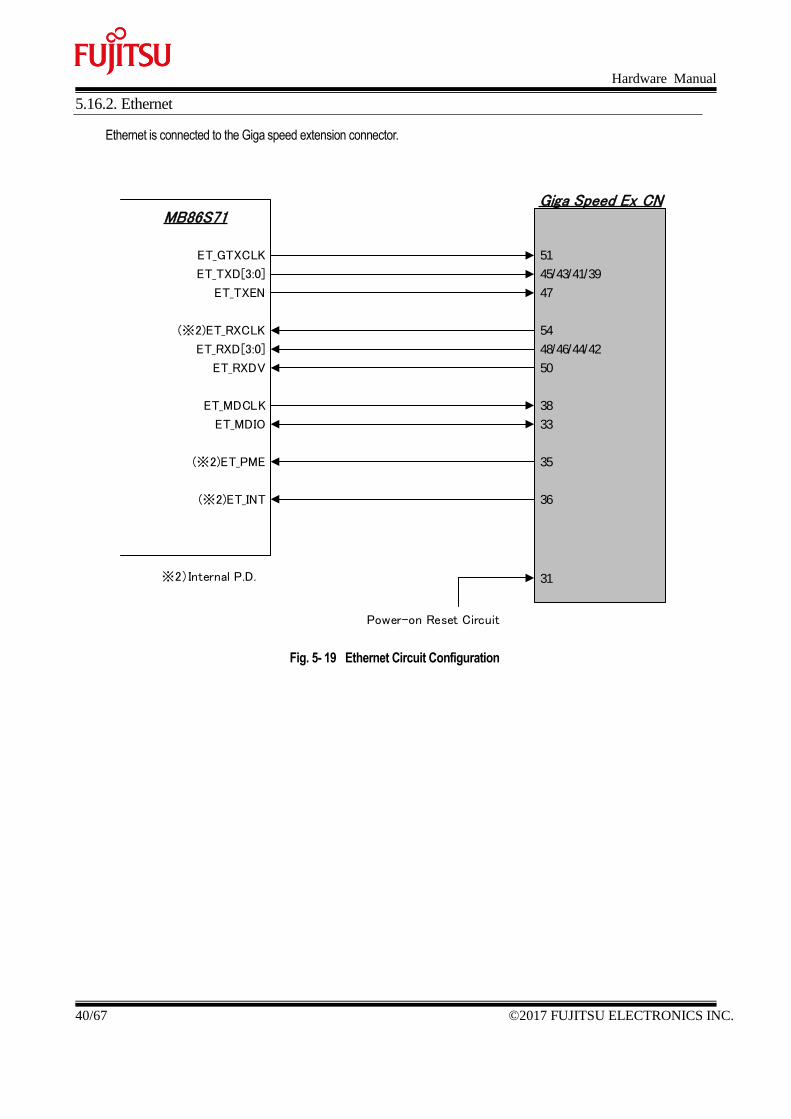
5.16.2. Ethernet
Ethernet is connected to the Giga speed extension connector.
MB86S71
ET_GTXCLK
ET_TXD[3:0]
(※2)ET_RXCLK
ET_RXD[3:0]
ET_TXEN
ET_RXDV
ET_MDCLK
ET_MDIO
(※2)ET_PME
(※2)ET_INT
※2)Internal P.D.
Power-on Reset Circuit
51
45/43/41/39
47
54
48/46/44/42
50
38
33
35
36
31
Giga Speed Ex CN
Fig. 5- 19 Ethernet Circuit Configuration
Hardware Manual
©2017 FUJITSU ELECTRONICS INC. 41/67
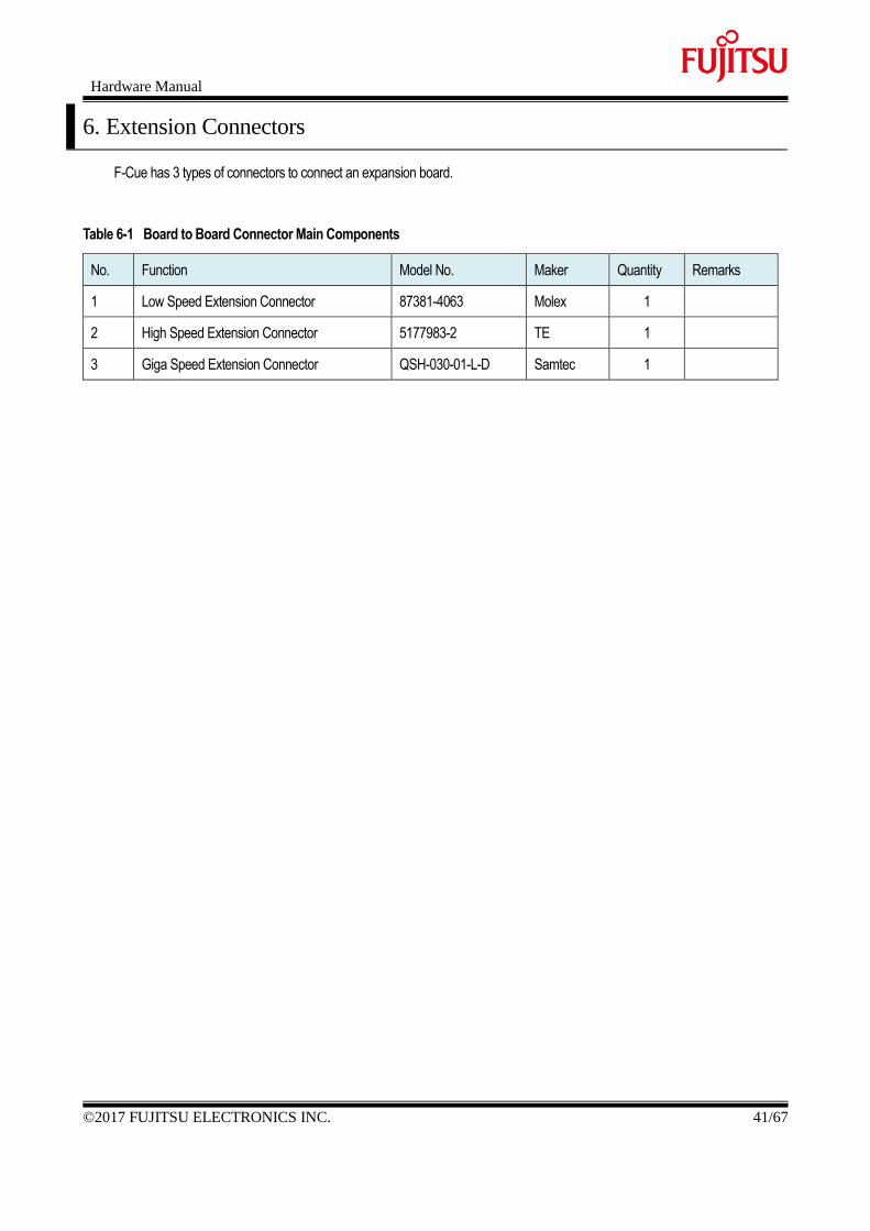
6. Extension Connectors
F-Cue has 3 types of connectors to connect an expansion board.
Table 6-1 Board to Board Connector Main Components
No. Function Model No. Maker Quantity Remarks
1 Low Speed Extension Connector 87381-4063 Molex 1
2 High Speed Extension Connector 5177983-2 TE 1
3 Giga Speed Extension Connector QSH-030-01-L-D Samtec 1
Hardware Manual
42/67 ©2017 FUJITSU ELECTRONICS INC.
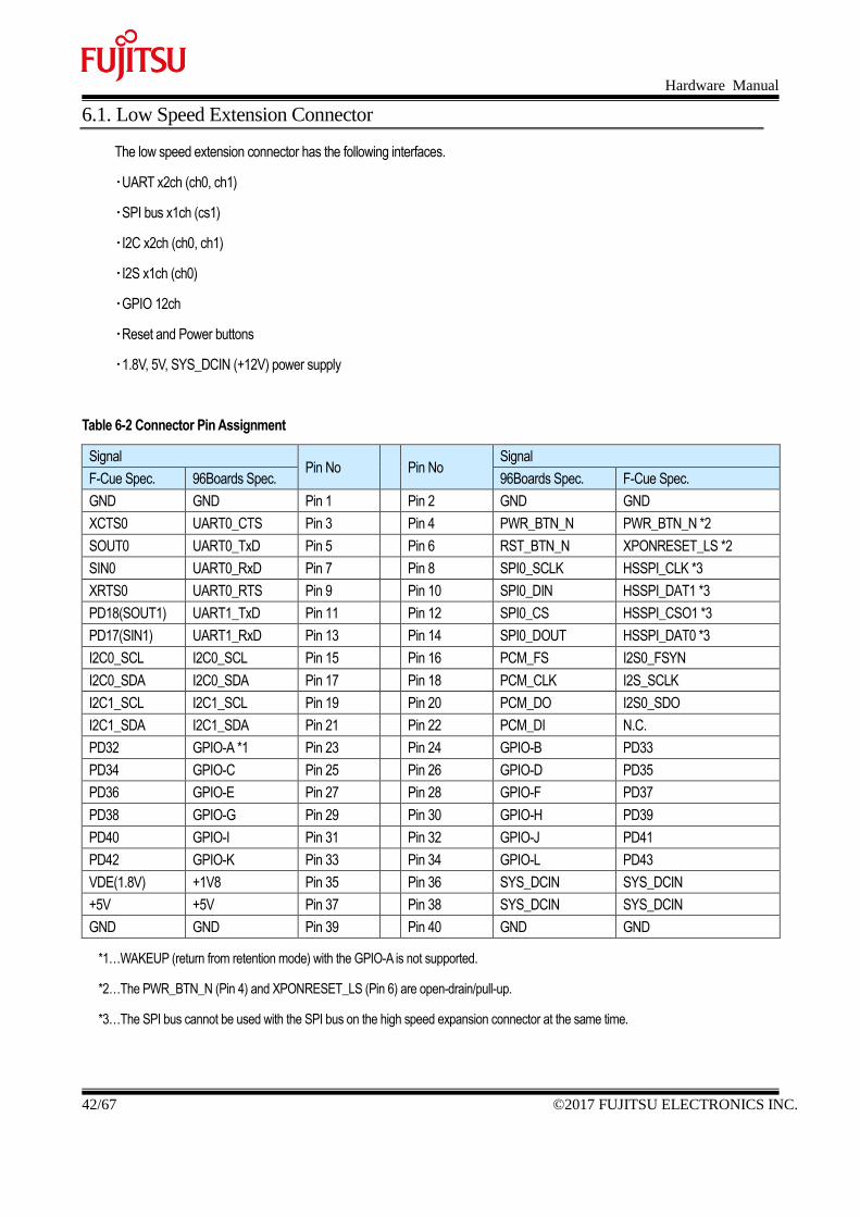
6.1. Low Speed Extension Connector
The low speed extension connector has the following interfaces.
・UART x2ch (ch0, ch1)
・SPI bus x1ch (cs1)
・I2C x2ch (ch0, ch1)
・I2S x1ch (ch0)
・GPIO 12ch
・Reset and Power buttons
・1.8V, 5V, SYS_DCIN (+12V) power supply
Table 6-2 Connector Pin Assignment
Signal Pin No Pin No
Signal
F-Cue Spec. 96Boards Spec. 96Boards Spec. F-Cue Spec.
GND GND Pin 1 Pin 2 GND GND
XCTS0 UART0_CTS Pin 3 Pin 4 PWR_BTN_N PWR_BTN_N *2
SOUT0 UART0_TxD Pin 5 Pin 6 RST_BTN_N XPONRESET_LS *2
SIN0 UART0_RxD Pin 7 Pin 8 SPI0_SCLK HSSPI_CLK *3
XRTS0 UART0_RTS Pin 9 Pin 10 SPI0_DIN HSSPI_DAT1 *3
PD18(SOUT1) UART1_TxD Pin 11 Pin 12 SPI0_CS HSSPI_CSO1 *3
PD17(SIN1) UART1_RxD Pin 13 Pin 14 SPI0_DOUT HSSPI_DAT0 *3
I2C0_SCL I2C0_SCL Pin 15 Pin 16 PCM_FS I2S0_FSYN
I2C0_SDA I2C0_SDA Pin 17 Pin 18 PCM_CLK I2S_SCLK
I2C1_SCL I2C1_SCL Pin 19 Pin 20 PCM_DO I2S0_SDO
I2C1_SDA I2C1_SDA Pin 21 Pin 22 PCM_DI N.C.
PD32 GPIO-A *1 Pin 23 Pin 24 GPIO-B PD33
PD34 GPIO-C Pin 25 Pin 26 GPIO-D PD35
PD36 GPIO-E Pin 27 Pin 28 GPIO-F PD37
PD38 GPIO-G Pin 29 Pin 30 GPIO-H PD39
PD40 GPIO-I Pin 31 Pin 32 GPIO-J PD41
PD42 GPIO-K Pin 33 Pin 34 GPIO-L PD43
VDE(1.8V) +1V8 Pin 35 Pin 36 SYS_DCIN SYS_DCIN
+5V +5V Pin 37 Pin 38 SYS_DCIN SYS_DCIN
GND GND Pin 39 Pin 40 GND GND
*1…WAKEUP (return from retention mode) with the GPIO-A is not supported.
*2…The PWR_BTN_N (Pin 4) and XPONRESET_LS (Pin 6) are open-drain/pull-up.
*3…The SPI bus cannot be used with the SPI bus on the high speed expansion connector at the same time.
Hardware Manual
©2017 FUJITSU ELECTRONICS INC. 43/67
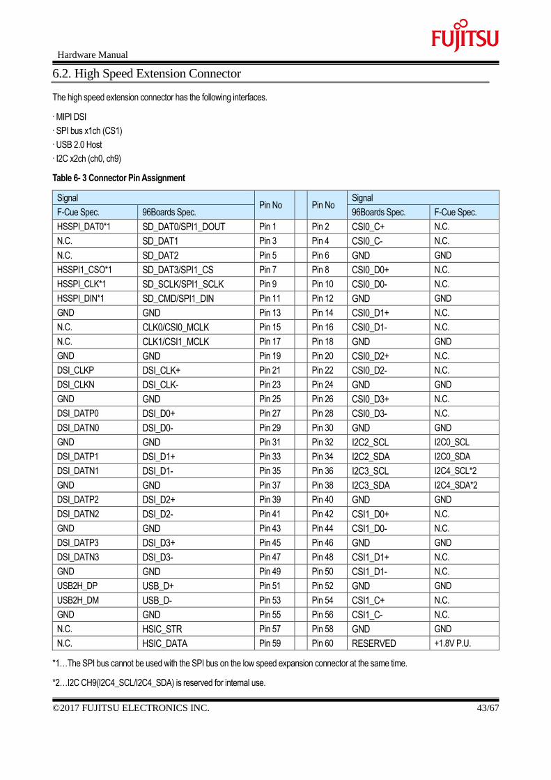
6.2. High Speed Extension Connector
The high speed extension connector has the following interfaces.
・MIPI DSI
・SPI bus x1ch (CS1)
・USB 2.0 Host
・I2C x2ch (ch0, ch9)
Table 6- 3 Connector Pin Assignment
Signal Pin No Pin No
Signal
F-Cue Spec. 96Boards Spec. 96Boards Spec. F-Cue Spec.
HSSPI_DAT0*1 SD_DAT0/SPI1_DOUT Pin 1 Pin 2 CSI0_C+ N.C.
N.C. SD_DAT1 Pin 3 Pin 4 CSI0_C- N.C.
N.C. SD_DAT2 Pin 5 Pin 6 GND GND
HSSPI1_CSO*1 SD_DAT3/SPI1_CS Pin 7 Pin 8 CSI0_D0+ N.C.
HSSPI_CLK*1 SD_SCLK/SPI1_SCLK Pin 9 Pin 10 CSI0_D0- N.C.
HSSPI_DIN*1 SD_CMD/SPI1_DIN Pin 11 Pin 12 GND GND
GND GND Pin 13 Pin 14 CSI0_D1+ N.C.
N.C. CLK0/CSI0_MCLK Pin 15 Pin 16 CSI0_D1- N.C.
N.C. CLK1/CSI1_MCLK Pin 17 Pin 18 GND GND
GND GND Pin 19 Pin 20 CSI0_D2+ N.C.
DSI_CLKP DSI_CLK+ Pin 21 Pin 22 CSI0_D2- N.C.
DSI_CLKN DSI_CLK- Pin 23 Pin 24 GND GND
GND GND Pin 25 Pin 26 CSI0_D3+ N.C.
DSI_DATP0 DSI_D0+ Pin 27 Pin 28 CSI0_D3- N.C.
DSI_DATN0 DSI_D0- Pin 29 Pin 30 GND GND
GND GND Pin 31 Pin 32 I2C2_SCL I2C0_SCL
DSI_DATP1 DSI_D1+ Pin 33 Pin 34 I2C2_SDA I2C0_SDA
DSI_DATN1 DSI_D1- Pin 35 Pin 36 I2C3_SCL I2C4_SCL*2
GND GND Pin 37 Pin 38 I2C3_SDA I2C4_SDA*2
DSI_DATP2 DSI_D2+ Pin 39 Pin 40 GND GND
DSI_DATN2 DSI_D2- Pin 41 Pin 42 CSI1_D0+ N.C.
GND GND Pin 43 Pin 44 CSI1_D0- N.C.
DSI_DATP3 DSI_D3+ Pin 45 Pin 46 GND GND
DSI_DATN3 DSI_D3- Pin 47 Pin 48 CSI1_D1+ N.C.
GND GND Pin 49 Pin 50 CSI1_D1- N.C.
USB2H_DP USB_D+ Pin 51 Pin 52 GND GND
USB2H_DM USB_D- Pin 53 Pin 54 CSI1_C+ N.C.
GND GND Pin 55 Pin 56 CSI1_C- N.C.
N.C. HSIC_STR Pin 57 Pin 58 GND GND
N.C. HSIC_DATA Pin 59 Pin 60 RESERVED +1.8V P.U.
*1…The SPI bus cannot be used with the SPI bus on the low speed expansion connector at the same time.
*2…I2C CH9(I2C4_SCL/I2C4_SDA) is reserved for internal use.
Hardware Manual
44/67 ©2017 FUJITSU ELECTRONICS INC.
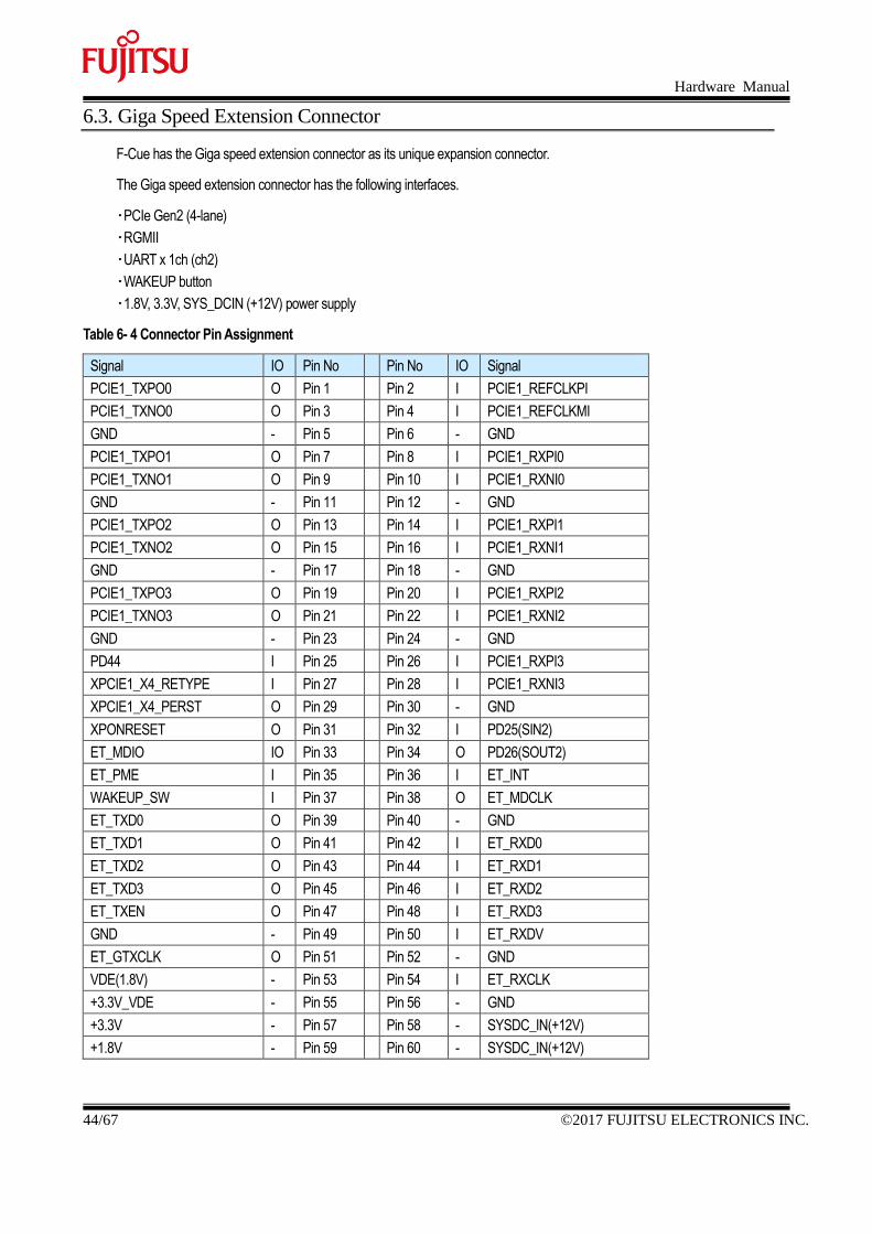
6.3. Giga Speed Extension Connector
F-Cue has the Giga speed extension connector as its unique expansion connector.
The Giga speed extension connector has the following interfaces.
・PCIe Gen2 (4-lane)
・RGMII
・UART x 1ch (ch2)
・WAKEUP button
・1.8V, 3.3V, SYS_DCIN (+12V) power supply
Table 6- 4 Connector Pin Assignment
Signal IO Pin No Pin No IO Signal
PCIE1_TXPO0 O Pin 1 Pin 2 I PCIE1_REFCLKPI
PCIE1_TXNO0 O Pin 3 Pin 4 I PCIE1_REFCLKMI
GND - Pin 5 Pin 6 - GND
PCIE1_TXPO1 O Pin 7 Pin 8 I PCIE1_RXPI0
PCIE1_TXNO1 O Pin 9 Pin 10 I PCIE1_RXNI0
GND - Pin 11 Pin 12 - GND
PCIE1_TXPO2 O Pin 13 Pin 14 I PCIE1_RXPI1
PCIE1_TXNO2 O Pin 15 Pin 16 I PCIE1_RXNI1
GND - Pin 17 Pin 18 - GND
PCIE1_TXPO3 O Pin 19 Pin 20 I PCIE1_RXPI2
PCIE1_TXNO3 O Pin 21 Pin 22 I PCIE1_RXNI2
GND - Pin 23 Pin 24 - GND
PD44 I Pin 25 Pin 26 I PCIE1_RXPI3
XPCIE1_X4_RETYPE I Pin 27 Pin 28 I PCIE1_RXNI3
XPCIE1_X4_PERST O Pin 29 Pin 30 - GND
XPONRESET O Pin 31 Pin 32 I PD25(SIN2)
ET_MDIO IO Pin 33 Pin 34 O PD26(SOUT2)
ET_PME I Pin 35 Pin 36 I ET_INT
WAKEUP_SW I Pin 37 Pin 38 O ET_MDCLK
ET_TXD0 O Pin 39 Pin 40 - GND
ET_TXD1 O Pin 41 Pin 42 I ET_RXD0
ET_TXD2 O Pin 43 Pin 44 I ET_RXD1
ET_TXD3 O Pin 45 Pin 46 I ET_RXD2
ET_TXEN O Pin 47 Pin 48 I ET_RXD3
GND - Pin 49 Pin 50 I ET_RXDV
ET_GTXCLK O Pin 51 Pin 52 - GND
VDE(1.8V) - Pin 53 Pin 54 I ET_RXCLK
+3.3V_VDE - Pin 55 Pin 56 - GND
+3.3V - Pin 57 Pin 58 - SYSDC_IN(+12V)
+1.8V - Pin 59 Pin 60 - SYSDC_IN(+12V)
Hardware Manual
©2017 FUJITSU ELECTRONICS INC. 45/67
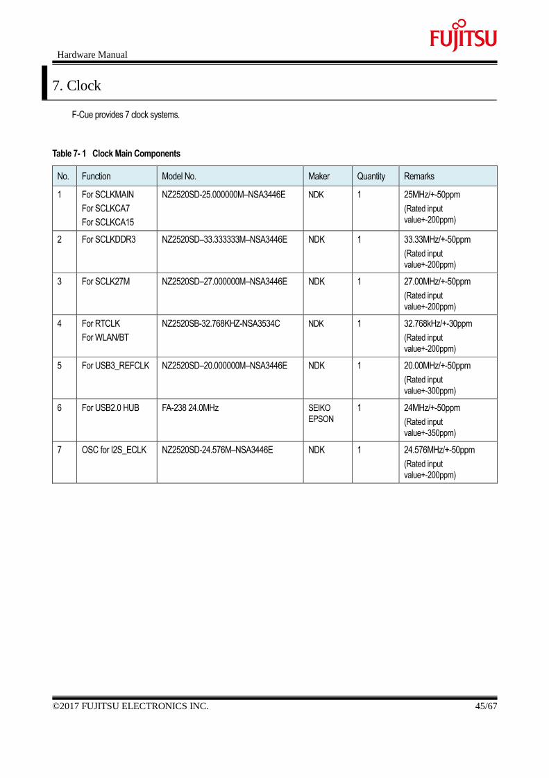
7. Clock
F-Cue provides 7 clock systems.
Table 7- 1 Clock Main Components
No. Function Model No. Maker Quantity Remarks
1 For SCLKMAIN
For SCLKCA7
For SCLKCA15
NZ2520SD-25.000000M–NSA3446E NDK 1 25MHz/+-50ppm
(Rated input
value+-200ppm)
2 For SCLKDDR3 NZ2520SD–33.333333M–NSA3446E NDK 1 33.33MHz/+-50ppm
(Rated input
value+-200ppm)
3 For SCLK27M NZ2520SD–27.000000M–NSA3446E NDK 1 27.00MHz/+-50ppm
(Rated input
value+-200ppm)
4 For RTCLK
For WLAN/BT
NZ2520SB-32.768KHZ-NSA3534C NDK 1 32.768kHz/+-30ppm
(Rated input
value+-200ppm)
5 For USB3_REFCLK NZ2520SD–20.000000M–NSA3446E NDK 1 20.00MHz/+-50ppm
(Rated input
value+-300ppm)
6 For USB2.0 HUB FA-238 24.0MHz SEIKO
EPSON
1 24MHz/+-50ppm
(Rated input
value+-350ppm)
7 OSC for I2S_ECLK NZ2520SD-24.576M–NSA3446E NDK 1 24.576MHz/+-50ppm
(Rated input
value+-200ppm)
Hardware Manual
46/67 ©2017 FUJITSU ELECTRONICS INC.
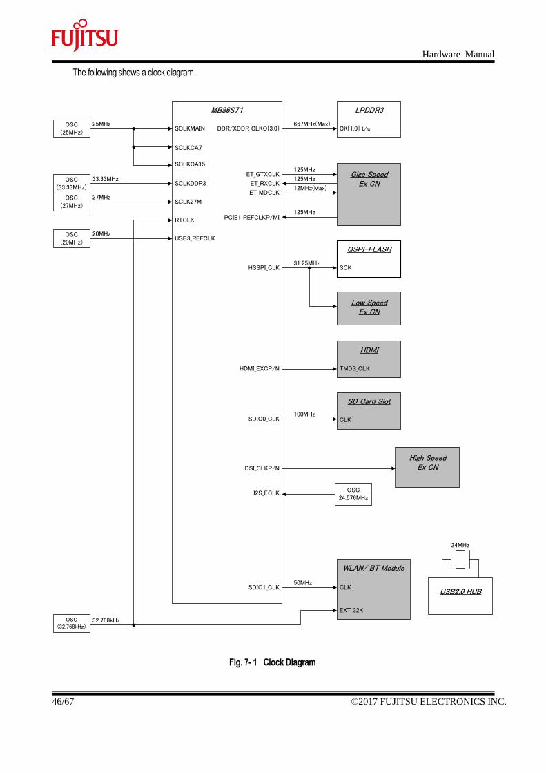
The following shows a clock diagram.
OSC(25MHz)
MB86S71
SCLKMAIN
SCLKDDR3
SCLK27M
RTCLK
25MHz
OSC(33.33MHz)
33.33MHz
OSC(27MHz)
27MHz
32.768kHz
ET_GTXCLK125MHz
ET_RXCLK
ET_MDCLK12MHz(Max)
125MHz
HSSPI_CLK
QSPI-FLASH
SCK31.25MHz
HDMI_EXCP/N
HDMI
TMDS_CLK
DSI_CLKP/N
SD Card Slot
CLK100MHz
SDIO0_CLK
OSC24.576MHz
I2S_ECLK
LPDDR3
CK[1:0]_t/cDDR/XDDR_CLKO[3:0]667MHz(Max)
EXT_32K
OSC(20MHz)
20MHzUSB3_REFCLK
SCLKCA7
SCLKCA15
OSC(32.768kHz)
WLAN/ BT Module
CLK50MHz
SDIO1_CLK
PCIE1_REFCLKP/MI
Giga Speed Ex CN
125MHz
Low Speed Ex CN
High Speed Ex CN
USB2.0 HUB
24MHz
Fig. 7- 1 Clock Diagram
Hardware Manual
©2017 FUJITSU ELECTRONICS INC. 47/67
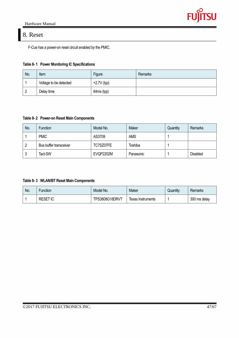
8. Reset
F-Cue has a power-on reset circuit enabled by the PMIC.
Table 8- 1 Power Monitoring IC Specifications
No. Item Figure Remarks
1 Voltage to be detected +2.7V (typ)
2 Delay time 64ms (typ)
Table 8- 2 Power-on Reset Main Components
No. Function Model No. Maker Quantity Remarks
1 PMIC AS3709 AMS 1
2 Bus buffer transceiver TC7SZ07FE Toshiba 1
3 Tact-SW EVQP2202M Panasonic 1 Disabled
Table 8- 3 WLAN/BT Reset Main Components
No. Function Model No. Maker Quantity Remarks
1 RESET IC TPS3808G18DRVT Texas Instruments 1 300 ms delay
Hardware Manual
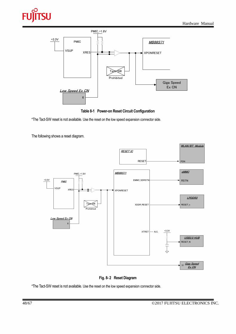
48/67 ©2017 FUJITSU ELECTRONICS INC.
PMIC
VSUP
+3.3V
XRES XPONRESET
Low Speed Ex CN
6
PMIC_+1.8V
MB86S71
Giga Speed Ex CN
Tact-SW
Prohibited
Table 8-1 Power-on Reset Circuit Configuration
*The Tact-SW reset is not available. Use the reset on the low speed expansion connector side.
The following shows a reset diagram.
eMMC
RSTN
MB86S71
XPONRESET
XTRST
XDDR_RESET
LPDDR3
RESET_n
USB2.0 HUB
RESET_N
EMMC_SDRSTN
RESET IC
RESET PDN
WLAN/BT Module
PMIC
VSUP
+3.3V
XRES
Low Speed Ex CN
6
PMIC_+1.8V
Giga Speed Ex CN
N.C.
31
+3.3V
Tact-SW
Prohibited
Fig. 8- 2 Reset Diagram
*The Tact-SW reset is not available. Use the reset on the low speed expansion connector side.
Hardware Manual
©2017 FUJITSU ELECTRONICS INC. 49/67
9. Power Management Overview
9.1. DC Power Input
The +12V (+-5%) power is supplied from the DC jack.
Power cannot be supplied from the low speed extension connector or a USB connector.
Table 9- 1 Power Supply Main Components
No. Function Model No. Maker Quantity Remarks
1 For +5V TPS54226RGTR TI 1 Io=2000mA (max)
2 For +3.3V TPS54527DDA TI 1 Io=5000mA (max)
3 PMIC AS3709-BQFR-xx AMS 1 DCDCx5, LDOx2
4 For +1.0V TPS62085RLTT TI 1 Io=3000mA (max)
5 DC Jack PJ-041H CUI 1 Center 1.65mm
6 Poly switch miniSMDC260F/13.2 Littelfuse 1 Vmax=13.2 V
Ihold=2.6 A (Ta=20°C)
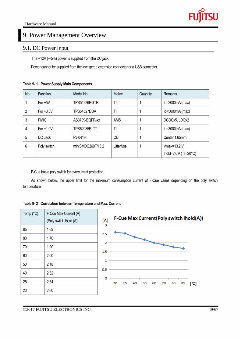
F-Cue has a poly switch for overcurrent protection.
As shown below, the upper limit for the maximum consumption current of F-Cue varies depending on the poly switch
temperature.
Table 9- 2 Correlation between Temperature and Max. Current
Temp (°C) F-Cue Max Current (A)
(Poly switch Ihold (A))
85 1.69
80 1.76
70 1.90
60 2.00
50 2.18
40 2.32
25 2.54
20 2.60
Hardware Manual
50/67 ©2017 FUJITSU ELECTRONICS INC.
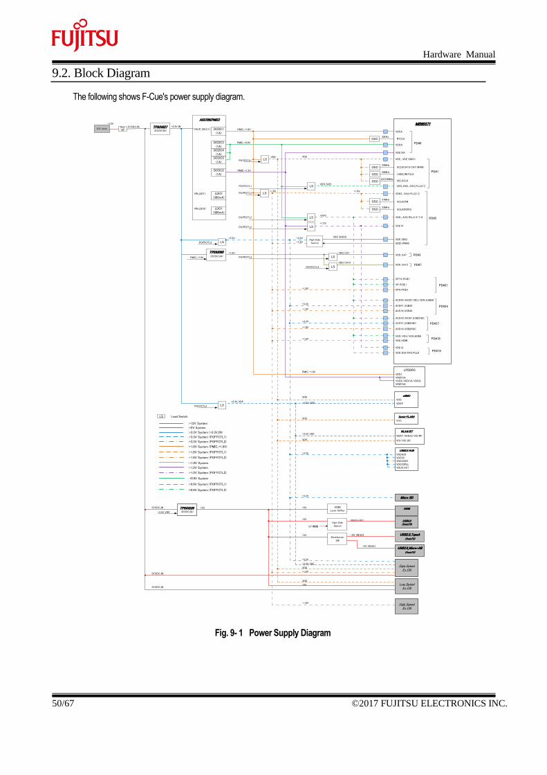
9.2. Block Diagram
The following shows F-Cue's power supply diagram.
TPS62085(DCDC:3A)
High Side Switch
LPDDR3
Serial-FLASH
High Side Switch
VDD1VREFCAVVD2/VDDCA/VDDQVREFDQ
VCC
USB3.0(Host:FS)
VBUS(+5V)
S71制御
USB2.0_TypeA(Host:FS)
USB2.0_Micro-AB(Host:FS)
+1.0V
LS
LS
OSC25MHz
OSC27MHz
OSC33MHz
OSC32kHz
MB86S71
VDD_SCB、AVD_PLL[2:1]
VDD_CA7
VDE、VDE_SDIO1
VDE2、VAA_PLL[2:1]
VDE_SDIO
VDE15A
VDE15
VDD、AVD_PLL3/5/7/8
VDDA
AVDF1_USB2HDC
AVDF2/AVDP_USB2HDC
AVD18_USB2HDC
SDIO_PWR0
VDEA
PD#0
PD#1
PD#2
PD#3
PD#27
VDD_CA15 PD#7
AVDF1_USB30
AVDF2/AVDP/VDU/VDN_USB30
AVD18_USB30
PD#24
VDD/VDU/VDN_HDMI
VDE_HDMIPD#18
VDE12
VDD_DSI/AVD_PLL6PD#19
SCLKCA15/CA7/MAIN
SCLK27M
SCLKDDR3
RTCLK
POFFCTL3
POFFCTL4
VDD_CA7
VDD_CA15
OSC20MHz
USB3_REFCLK
+3.3V
USB2.0 HUB
VDDA33VDD33VDD33CRVDD33PLLVBUS_DET
AS3709(PMIC)
DCDC3(1A)
LDO1(300mA)
VIN_LDO1
VSUP_SD[5:1]
VIN_LDO2
DCDC4(1A)
DCDC5(1A)
DCDC1(1A)
DCDC2(1A)
LDO1(300mA)
WLAN/BT
VBAT/VDD33/VIO_RF
VIO/VIO_SD
DC-Jack+3.3V_INTPS54527
(DCDC:5A)
+12V
TPS54226(DCDC:2A)
LSPOFFCTL2
+5V
:+12V System
:+5V System
:+1.2V System
:+1.0V System
LS Load Switch
VP_PCIE1
VPTX_PCIE1
VPH_PCIE1
PD#21
Giga SpeedEx CN
Low SpeedEx CN
LSVDE
LS
PMIC_+1.8V
POFFCTL1
POFFCTL2
LSPOFFCTL1VDD_SCB
+0.9VLSPOFFCTL2
PMIC_+0.9V
PMIC_+1.2V
LSPOFFCTL2
+1.2V
+1.8V
eMMC
VDD
VDDFLSPOFFCTL1
+3.3V_VDE
DistributionSW
+5V_VBUS2
+5V_VBUS1
Micro SD
HDMILevel Shifter
HDMI
:+3.3V System (POFFCTL1)
:+3.3V System (POFFCTL2)
:+3.3V System (+3.3V_IN)
:+1.8V System (PMIC_+1.8V)
:+1.8V System (POFFCTL1)
:+1.8V System (POFFCTL2)
:+1.2V System (POFFCTL2)
:+0.9V System
:+0.9V System (POFFCTL1)
:+0.9V System (POFFCTL2)
+3.3V_VDE
+3.3V_VDE
+3.3V_VDE
+3.3V
+3.3V
+3.3V
+3.3V
+3.3V
+3.3V
VDE
VDE
+1.8V
+1.8V
VDE
VDE
VDE
PMIC_+1.8V
+1.8V
+1.8V
+1.8V
+1.8V
VDE
SYSDC_IN
SYSDC_IN
SYSDC_IN
PolySW
SYSDC_IN
+5V
+5V
+5V
+5V
+3.3V_VDE
PMIC_+1.8V
VDE_SDIO0
+1.8V
High SpeedEx CN
+1.8V
OSC24.576MHz
I2S_ECLK
Fig. 9- 1 Power Supply Diagram
Hardware Manual
©2017 FUJITSU ELECTRONICS INC. 51/67
Table 9- 3 Power Supply Control Use Case
Status POFFCTL Setting Remarks
[0] [1] [2] [3] [4]
Retention Power ON Power OFF Power OFF Power OFF Power OFF PD#0
All functions in
operation
Power ON Power ON Power ON Power ON Power ON
*For details on POFFCTL, refer to the MB86S71 data sheet.
9.3. Power Sequencing
Pressing the power switch turns ON the power of the board.
When power is ON, if you press and hold the power switch for 2 seconds or longer and then release it, the software turns OFF the
power of the board.
(Normally, it is recommended that the power be turned OFF by using the shutdown command.)
9.4. Power Supplies
The total current supplied from the 5 V system (HDMI, USB3.0 Type A, USB2.0 Type A, Low Speed Extension Connector) to
external devices is limited to 2A.
*The HDMI, USB3.0, USB2.0, and low speed expansion connector can supply 0.1A, 0.9A, 0.5A, and 1.0A, respectively. However,
the upper limit for the total is 2.0 A.
Table 9- 4 5V Power Supplies
+5V Line Standard value(Max)
HDMI 0.1A
USB3.0 0.9A
USB2.0 0.5A
Low Speed EX CN 1.0A
F-Cue Spec
Total 2A Upper Limit.
Hardware Manual
52/67 ©2017 FUJITSU ELECTRONICS INC.
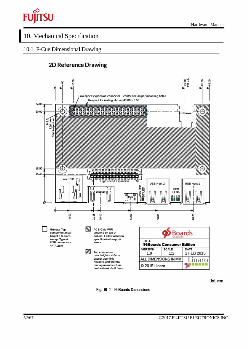
10. Mechanical Specification
10.1. F-Cue Dimensional Drawing
Unit: mm
Fig. 10- 1 96 Boards Dimensions
Hardware Manual
©2017 FUJITSU ELECTRONICS INC. 53/67
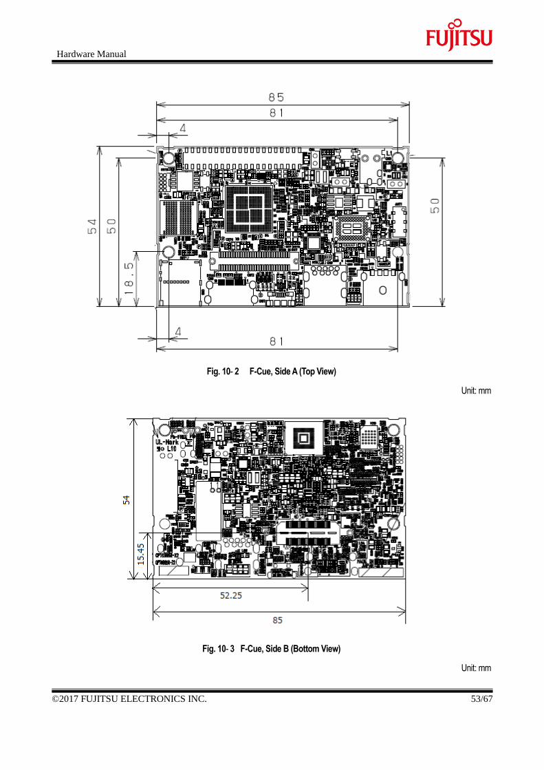
Fig. 10- 2 F-Cue, Side A (Top View)
Unit: mm
Fig. 10- 3 F-Cue, Side B (Bottom View)
Unit: mm
Hardware Manual
54/67 ©2017 FUJITSU ELECTRONICS INC.
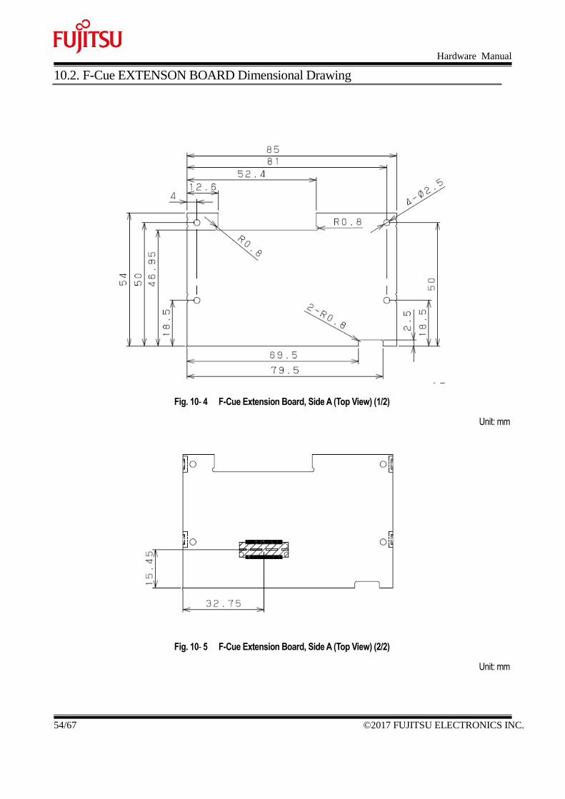
10.2. F-Cue EXTENSON BOARD Dimensional Drawing
Fig. 10- 4 F-Cue Extension Board, Side A (Top View) (1/2)
Unit: mm
Fig. 10- 5 F-Cue Extension Board, Side A (Top View) (2/2)
Unit: mm
Hardware Manual
©2017 FUJITSU ELECTRONICS INC. 55/67
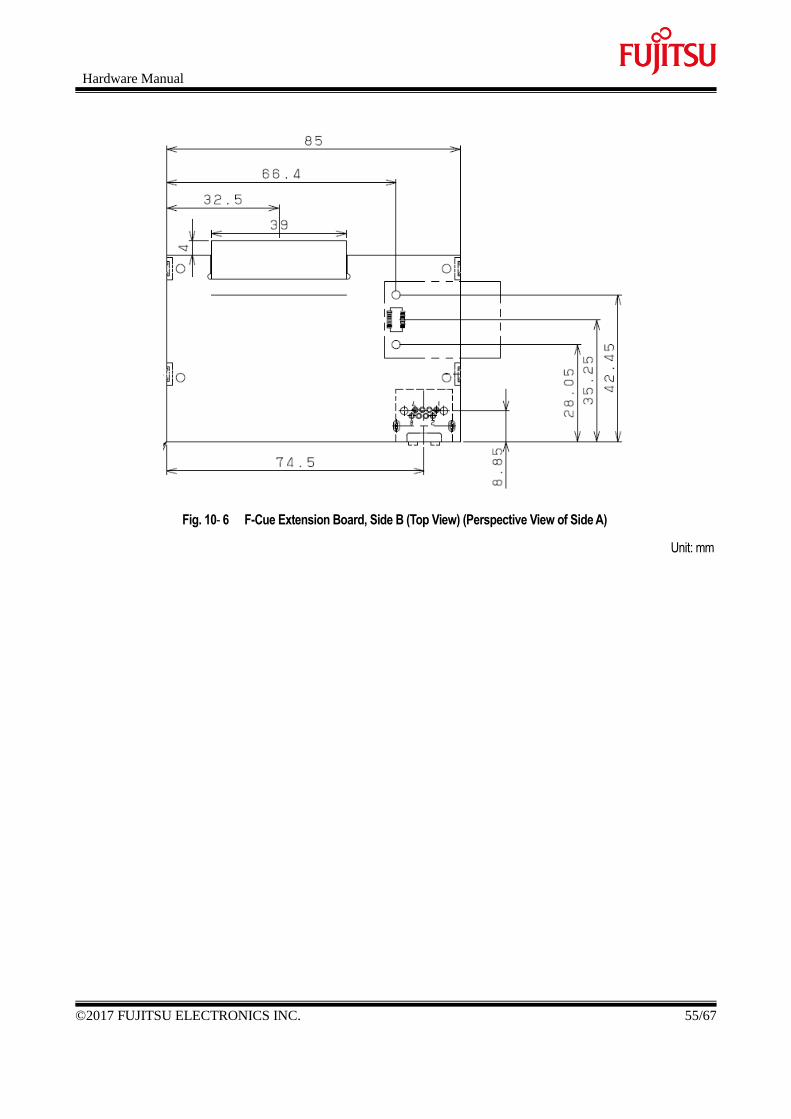
Fig. 10- 6 F-Cue Extension Board, Side B (Top View) (Perspective View of Side A)
Unit: mm
Hardware Manual
56/67 ©2017 FUJITSU ELECTRONICS INC.
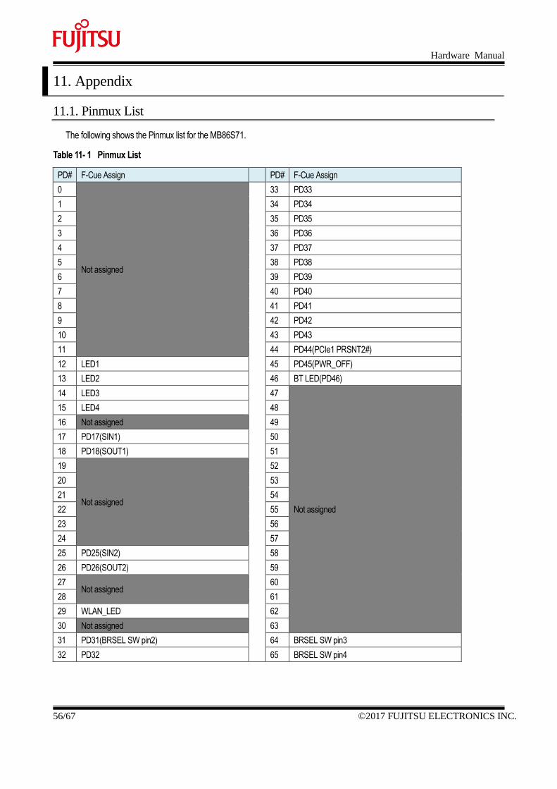
11. Appendix
11.1. Pinmux List
The following shows the Pinmux list for the MB86S71.
Table 11- 1 Pinmux List
PD# F-Cue Assign PD# F-Cue Assign
0
Not assigned
33 PD33
1 34 PD34
2 35 PD35
3 36 PD36
4 37 PD37
5 38 PD38
6 39 PD39
7 40 PD40
8 41 PD41
9 42 PD42
10 43 PD43
11 44 PD44(PCIe1 PRSNT2#)
12 LED1 45 PD45(PWR_OFF)
13 LED2 46 BT LED(PD46)
14 LED3 47
Not assigned
15 LED4 48
16 Not assigned 49
17 PD17(SIN1) 50
18 PD18(SOUT1) 51
19
Not assigned
52
20 53
21 54
22 55
23 56
24 57
25 PD25(SIN2) 58
26 PD26(SOUT2) 59
27 Not assigned
60
28 61
29 WLAN_LED 62
30 Not assigned 63
31 PD31(BRSEL SW pin2) 64 BRSEL SW pin3
32 PD32 65 BRSEL SW pin4
Hardware Manual
©2017 FUJITSU ELECTRONICS INC. 57/67
12. F-Cue EXTENSION Board (Option)
This is an extension board connected to F-Cue's dedicated connector and enables the following functions to be used.
・Wired LAN (RJ-45 connector)
・PCIe (PCIe expansion slot Gen2 4-Lane)
・UART x1ch
12.1. Prerequisites
Before powering on, you need to prepare the following.
・F-Cue
・F-Cue EXTENSION BOARD
・AC adapter (The TW-12020U AC adapter and SSCI-025461 converter plug are recommended)
・USB mouse and keyboard
・HDMI monitor and HDMI cable
12.2. Assembly Drawing
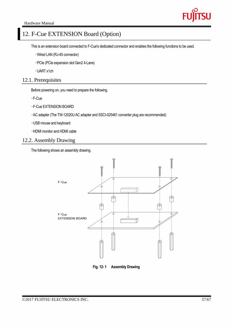
The following shows an assembly drawing.
F-Cue
F-Cue EXTENSION BOARD
Fig. 12- 1 Assembly Drawing
Hardware Manual
58/67 ©2017 FUJITSU ELECTRONICS INC.
12.3. First Power ON
The following describes the F-Cue startup procedure.
・Assemble F-Cue and the F-Cue EXTENSION BOARD.
・Connect F-Cue to the monitor using an HDMI cable.
・Connect the mouse and keyboard to F-Cue.
・Connect the AC adapter to the DC jack and an outlet.
・Press down the power switch.
12.4. Hardware Specification
This section describes the hardware specification overview.
Table 12- 1 F-Cue EXTENSION BOARD Hardware Specifications
Connecting Systems
No. Item Description Remarks
1 Ethernet
Ethernet-PHY×1, RJ-45×1, Transformer×1
Ethernet-PHY RTL8211E-VL-CG (Realtek)
Pulse transformer LFE9292A-R
(DELTA ELECTRONICS)
RJ-45 JM36113(FOXCONN)
2 PCIe
PCIe (Gen2 4-Lane)×1
PCIe PCIE-064-02-F-D-EMS2
(Samtec)
PCIe CLK Gen IDT5V41065PGG(IDT)
3 UART
UART×1 (ch2)
Interface connector 20P3.0-JMCS-G-TF(N) (JST)
4
Giga speed
extension
connector
Interface connector QTH-030-01-L-D-A (Samtec)
Hardware Manual
©2017 FUJITSU ELECTRONICS INC. 59/67
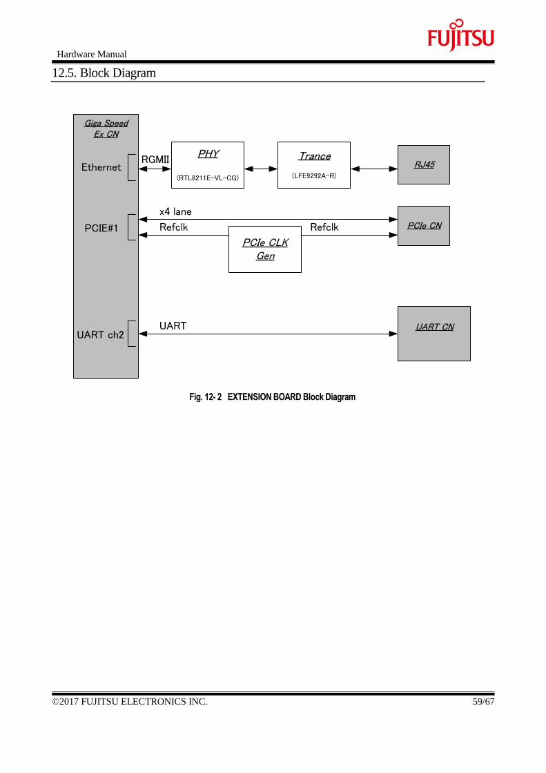
12.5. Block Diagram
Giga Speed Ex CN
PHY
(RTL8211E-VL-CG)
RJ45
PCIe CN
PCIe CLK Gen
Ethernet
PCIE#1
UART ch2UART CN
Trance
(LFE9292A-R)
x4 lane
Refclk Refclk
RGMII
UART
Fig. 12- 2 EXTENSION BOARD Block Diagram
Hardware Manual
60/67 ©2017 FUJITSU ELECTRONICS INC.
12.6. Component Details
12.6.1. Ethernet
F-Cue has 1 Ethernet port.
Table 12- 2 Ethernet Interface
No. Item Description Remarks
1 Compliant standard 10BASE-T, 100BASE-TX, and 1000BASE-T
WOL compatible
2 Connector RJ-45
3 PHY-Link I/F RGMII
Table 12-3 Ethernet Interface Main Components
No. Function Model No. Maker Quantity Remarks
1 RJ-45 JM36113 FOXCONN 1
2 Ethernet-PHY RTL8211E-VL-CG Realtek 1
3 Crystal oscillator FA-238 25.0000MHz SEIKO EPSON 1 25MHz +-20ppm
4 1Gate Inverter TC7SZ14FU Toshiba 2 Schmidt
5 Pulse transformer LFE9292A-R
DELTA
ELECTRONICS
1
6 Common mode noise filter ACM2520-301-2P-T002 TDK 4 300ohm/400mA/0.35ohm
Hardware Manual
©2017 FUJITSU ELECTRONICS INC. 61/67
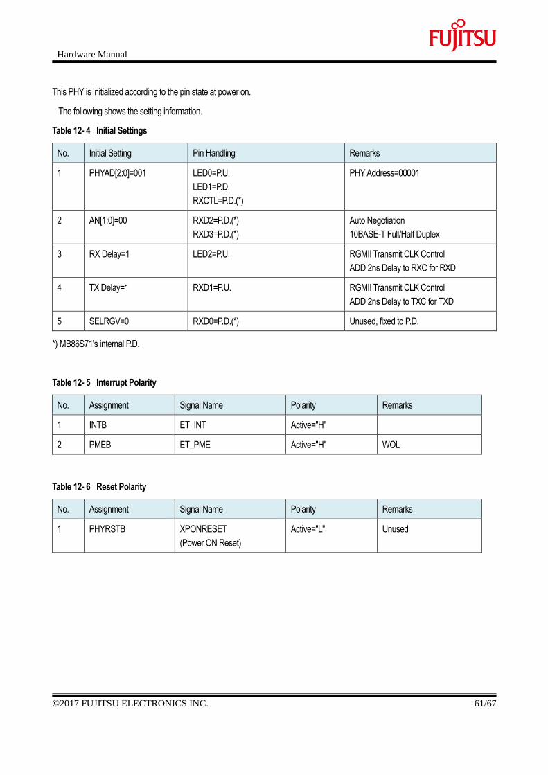
This PHY is initialized according to the pin state at power on.
The following shows the setting information.
Table 12- 4 Initial Settings
No. Initial Setting Pin Handling Remarks
1 PHYAD[2:0]=001 LED0=P.U.
LED1=P.D.
RXCTL=P.D.(*)
PHY Address=00001
2 AN[1:0]=00 RXD2=P.D.(*)
RXD3=P.D.(*)
Auto Negotiation
10BASE-T Full/Half Duplex
3 RX Delay=1 LED2=P.U. RGMII Transmit CLK Control
ADD 2ns Delay to RXC for RXD
4 TX Delay=1 RXD1=P.U. RGMII Transmit CLK Control
ADD 2ns Delay to TXC for TXD
5 SELRGV=0 RXD0=P.D.(*) Unused, fixed to P.D.
*) MB86S71's internal P.D.
Table 12- 5 Interrupt Polarity
No. Assignment Signal Name Polarity Remarks
1 INTB ET_INT Active="H"
2 PMEB ET_PME Active="H" WOL
Table 12- 6 Reset Polarity
No. Assignment Signal Name Polarity Remarks
1 PHYRSTB XPONRESET
(Power ON Reset)
Active="L" Unused
Hardware Manual
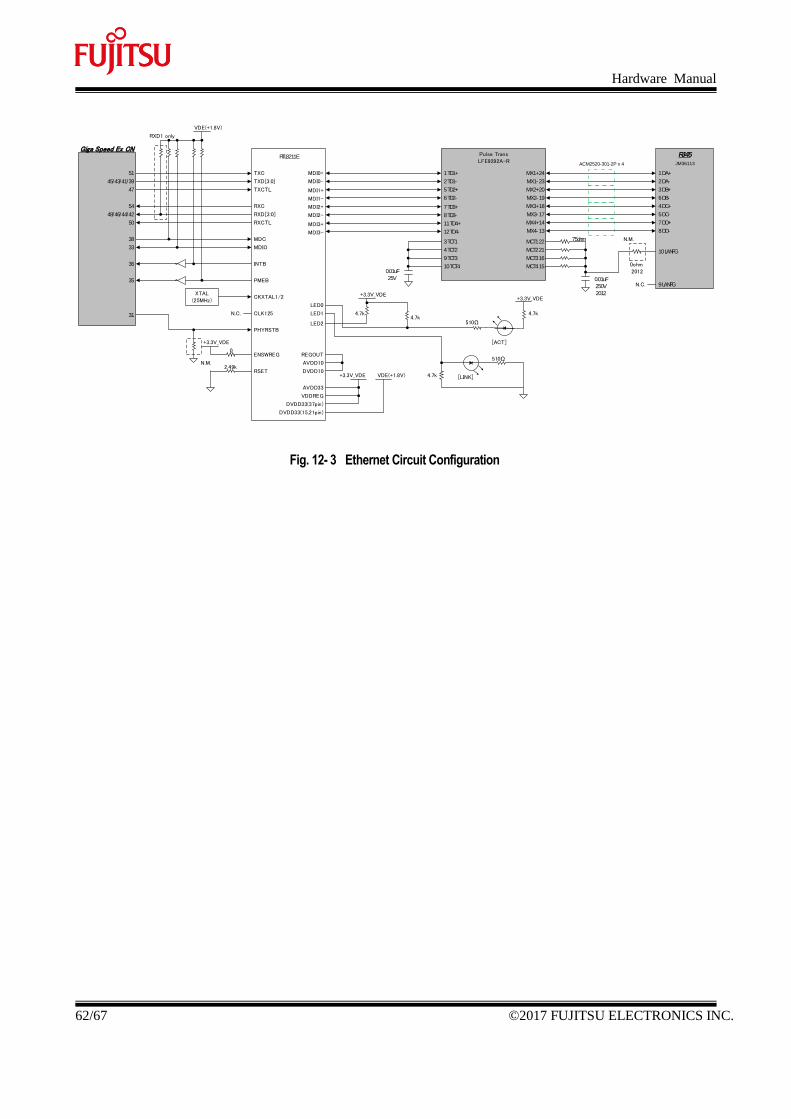
62/67 ©2017 FUJITSU ELECTRONICS INC.
XTAL(25MHz)
RTL8211E
VDE(+1.8V)
RXD1 only
TXC
TXD[3:0]
TXCTL
RXC
RXD[3:0]
RXCTL
MDC
MDIO
PMEB
INTB
CKXTAL1/2
ENSWREG
CLK125
REGOUT
VDDREG
RSET DVDD10
LED2
DVDD33(15,21pin)
AVDD10
AVDD33
N.C.
+3.3V_VDE
0
2.49k
MDI0+
MDI0-
MDI1+
MDI1-
MDI2+
MDI2-
MDI3+
MDI3-
LED0
LED1
RJ-45
JM36113
1 DA+
2 DA-
3 DB+
6 DB-
4 DC+
5 DC-
8 DD-
7 DD+
+3.3V_VDE VDE(+1.8V)
PHYRSTB
DVDD33(37pin)
+3.3V_VDE
N.M.
51
45/43/41/39
47
54
48/46/44/42
50
38
33
36
35
31
Giga Speed Ex CN
4.7k
Pulse TransLFE9292A-R
2 TD1-
1 TD1+
3 TCT1
5 TD2+
6 TD2-
4 TCT2
8 TD3-
7 TD3+
9 TCT3
11 TD4+
12 TD4-
10 TCT4
MX1- 23
MX1+ 24
MX2- 19
MX2+ 20
MX3- 17
MX3+ 18
MX4- 13
MX4+ 14
MCT1 22
MCT2 21
MCT3 16
MCT4 150.01uF
25V 0.01uF
250V
2012
75ohm
ACM2520-301-2P x 4
9 LANFG
10 LANFG
N.M.
0ohm2012
N.C.
+3.3V_VDE
4.7k
4.7k
510Ω
[ACT]
[LINK]
510Ω
4.7k
Fig. 12- 3 Ethernet Circuit Configuration
Hardware Manual
©2017 FUJITSU ELECTRONICS INC. 63/67
12.6.2. PCIe
F-Cue has the PCIe root complex connector (4-Lane). Endpoint is not supported.
Table 12- 7 PCIe Interface
No. Item Description Remarks
1 Function Root Complex
2 Compliant standard PCIe Gen2 (5Gbps)
3 Hot Swap Not supported
4 Wake Control Not supported
5 Number of lanes 4 Lanes
6 Connector 4-Lane Card Slot Root Complex
Table 12- 8 PCIe Main Components
No. Function Model No. Maker Quantity Remarks
1 PCIe Card Slot PCIE-064-02-F-D-EMS2 Samtec 1
2 Lv conversion buffer SN74LVC1T45DCK TI 1 1bit
3 Crystal oscillator FA-238 25.0000MHz SEIKO
EPSON
1 25MHz +-50ppm
4 PCIe CLK Gen 5V41065PGG IDT 1 2ch TSSOP-16
5 Slide SW CUS-22TB Copal Electronics
2 Double-pole, double-throw
6 Short plug JX-10 MAC8 4 For pin socket
7 Pin socket PD-7 MAC8 10
8 Short plug JS-1 MAC8 2 For PinHeader
9 PinHeader FFC-6BMEP1B Honda Tsushin 1 3x2pin
10 Diode RB031L-30FA ROHM 2 Schottky diode (5A)
Hardware Manual
64/67 ©2017 FUJITSU ELECTRONICS INC.
[PCIE1 TYPE]
[ROOT] [EP]
[PCIE1 PRSNT2]
[ROOT] [EP]
[PCIE1 REFCLK]
Root Complex settings
[PCIE1 PWR]
ROOT settings: 3-5pin short 4-6pin short +12V:Max 400mA +3.3V:Max 1A
■When power is supplied from the board
[PCIE1 PWR]
■
PCIe (ROOT) Power Setting
Fig. 12- 4 PCIe1 Root Setting
Table 12- 9 PCIe1 Root Setting
No. Item PCIE1 TYPE PCIE1 PRSNT2 REFCLK PCIE1 PWR Remarks
1 Root Complex ROOT ROOT ROOT SHORT
* Any settings other than the above are prohibited. Endpoint is not supported.
Table 12- 10 PRNST2# Detection Polarity
No. Item ch Signal Name Polarity Remarks
1 PRSNT2# PCIe1 PD44(PD2/EXINT26) L=Detection
Hardware Manual
©2017 FUJITSU ELECTRONICS INC. 65/67
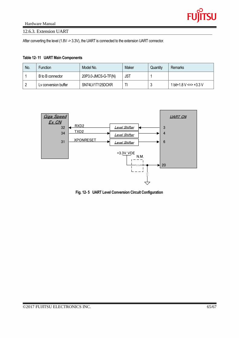
12.6.3. Extension UART
After converting the level (1.8V -> 3.3V), the UART is connected to the extension UART connector.
Table 12- 11 UART Main Components
No. Function Model No. Maker Quantity Remarks
1 B to B connector 20P3.0-JMCS-G-TF(N) JST 1
2 Lv conversion buffer SN74LV1T125DCKR TI 3 1 bit+1.8 V <=> +3.3 V
32
34
Giga Speed Ex CN
UART CN
3
4TXD2
RXD2 Level Shifter
31 XPONRESET 6
20
+3.3V_VDEN.M.
Level Shifter
Level Shifter
Fig. 12- 5 UART Level Conversion Circuit Configuration
Hardware Manual
66/67 ©2017 FUJITSU ELECTRONICS INC.
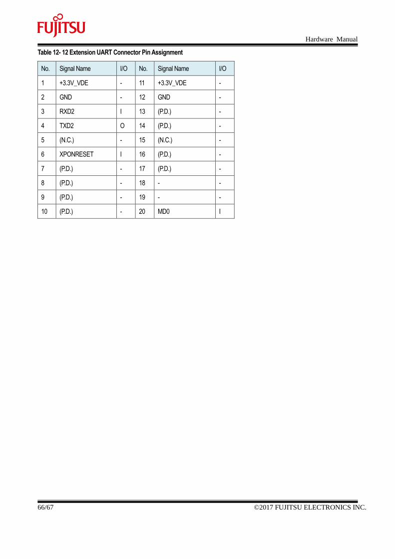
Table 12- 12 Extension UART Connector Pin Assignment
No. Signal Name I/O No. Signal Name I/O
1 +3.3V_VDE - 11 +3.3V_VDE -
2 GND - 12 GND -
3 RXD2 I 13 (P.D.) -
4 TXD2 O 14 (P.D.) -
5 (N.C.) - 15 (N.C.) -
6 XPONRESET I 16 (P.D.) -
7 (P.D.) - 17 (P.D.) -
8 (P.D.) - 18 - -
9 (P.D.) - 19 - -
10 (P.D.) - 20 MD0 I
Hardware Manual
©2017 FUJITSU ELECTRONICS INC. 67/67
Change History
Date Version Description
2017/01/17 1.00 First Edition
2017/01/25 1.01 Corrected an error in the description of the pin assignment for the low speed extension
connector in Fig. 4-12 UART Circuit Configuration.
Corrected an error in the description of the pin assignment for the Giga speed extension
connector.
2017/05/18 1.02 Fully revised in accordance with the “96boardsBoardHWUserManualtemplate” configuration.
Corrected an error in the description of "Table 12- 12 Extension UART Connector Pin
Assignment".