Extreme nanophotonics from ultrathin metallic gaps · 1NanoPhotonics Centre, Cavendish Laboratory,...
11
REVIEW ARTICLE https://doi.org/10.1038/s41563-019-0290-y 1 NanoPhotonics Centre, Cavendish Laboratory, University of Cambridge, Cambridge, UK. 2 Materials Physics Center CSIC-UPV/EHU and Donostia International Physics Center DIPC, Paseo Manuel de Lardizabal, Donostia-San Sebastiàn, Spain. 3 Center for Metamaterials and Integrated Plasmonics, Duke University, Durham, NC, USA. *e-mail: [email protected] P lasmonic nanostructures confine light to dimensions far smaller than the free-space wavelength, as they mix optical fields with electronic excitations. Highlighted from early on 1 , interest grew in the 1990s when local fields around nanostructures could be directly measured by near-field scanning optical micros- copy 2,3 . Plasmon nanostructures gained rapid appreciation as routes to optical devices unconstrained by the wavelength of light, yielding viable nanophotonic devices 4–6 . A metallic nanoparticle of gold, silver, copper or aluminium exhibits plasmon resonances at wavelengths determined by its mate- rial properties, shape and size. For metallic nanoparticles with sharp corners or protrusions, light can be strongly localized to volumes with minimum dimensions of 10–100 nm (refs. 7–10 ). Achieving even more tightly confined fields—on the scale of 1 nm or less—is possible but very difficult with single nanoparticles, since neither colloidal nor lithographic fabrication approaches offer reproduc- ible control over such small feature sizes. Many advanced optical phenomena, however, hinge on such tightly localized fields, and require the strongest field enhancements and localization possible, for instance to elicit surface-enhanced Raman scattering 11 (SERS) or photon blockade from single molecules. Coupling nanoparticle plasmons together represents an alterna- tive approach to field localization, as light can be tightly confined to the gaps between nanoparticles 12–14,15 . However, the same limitations in fabrication capabilities also lead to inconsistent control over gap dimensions in nanoparticle clusters 16 . Fortunately, the large field enhancements associated with nanoparticle clusters can also be achieved with single nanoparti- cles separated from a metal film by a thin dielectric layer, which behave similarly to a pair or dimer of nanoparticles 17–19 . In one realization for ultrahigh-vacuum environments, the gaps between scanning probe tips and metallic surfaces can produce well- controlled cavities where single-molecule spectroscopy is possible 20 (TERS). This plasmonic environment is capable of electrical excita- tion and high spatial resolutions 20,21,22 while other scanning systems have also been created by adhering or fabricating metal nano- structures onto atomic force microscopy tips or optical fibres 23 . However, for robust devices, the initial approach of top-down lithographic definition of gaps 24,25 has more recently been comple- mented by bottom-up self-assembly, which provides exquisitely defined gaps down to 0.3 nm (refs. 26–28 ). The ‘gap plasmons’ confined between two opposing metal sur- faces propagate similarly to a wave along a transmission line 29,30 . These gap modes have complex behaviours and enter the regime of ‘extreme nano-optics’ because they can be sensitive to single- atom placements. This geometry, which has been known variously as a nanopatch optical antenna, nanoparticle-on-mirror (NPoM), metastructure, metal–insulator–metal (MIM) waveguide, or par- ticle over surface, has become increasingly studied for a wide variety of optical phenomena. The attractiveness of the plasmonic nanopatch or NPoM stems from its ease of fabrication combined with the extreme field enhancements available in either colloidal or lithographically patterned systems. The plasmonic nanopatch has proven a remarkably successful and robust platform for dem- onstrating a wide variety of optical phenomena. In this Review, we focus specifically on the nanopatch, providing intuitive inter- pretations of its properties and exploring its use across different application areas. Recent demonstrations that light can be trapped in optical modes of nanogaps with rigorously defined mode volumes below 1 nm 3 from surface atoms 31 shows why nanogap plasmons are so important. Every gold surface supports adatoms, but normally the tight confinement into atomic-scale modes leads to negligi- ble interaction with free-space photons. Only due to impedance matching of the plasmonic antennas and nanogaps to free space is it now possible to couple into and out of these highly localized modes with high efficiencies >10% (Fig. 1). As a simple initial estimate, the effective impedance of a nanoantenna, compared to that of free space Z 0 operating at wavelength λ, scales with the current dipole length (ℓ) as 32 λ = ℓ∕ Z Z ( ) r 0 2 and hence the typi- cal power coupling efficiency into an atomically localized plasmon is λ ℓ ≈ - 4( / ) 10 2 6 . When there are intermediate stages through successively tighter-confined plasmon modes (Fig. 1), this coupling can be improved by five orders of magnitude, which is vital since optimizing antenna coupling is crucial for utilization in optoelectronic devices 33,34 . Extreme nanophotonics from ultrathin metallic gaps Jeremy J. Baumberg 1 *, Javier Aizpurua 2 , Maiken H. Mikkelsen 3 and David R. Smith 3 Ultrathin dielectric gaps between metals can trap plasmonic optical modes with surprisingly low loss and with volumes below 1 nm 3 . We review the origin and subtle properties of these modes, and show how they can be well accounted for by simple models. Particularly important is the mixing between radiating antennas and confined nanogap modes, which is extremely sensitive to precise nanogeometry, right down to the single-atom level. Coupling nanogap plasmons to electronic and vibronic transitions yields a host of phenomena including single-molecule strong coupling and molecular optomechanics, opening access to atomic-scale chemistry and materials science, as well as quantum metamaterials. Ultimate low-energy devices such as robust bottom-up assembled single-atom switches are thus in prospect. NATURE MATERIALS | www.nature.com/naturematerials
Transcript of Extreme nanophotonics from ultrathin metallic gaps · 1NanoPhotonics Centre, Cavendish Laboratory,...

Review ARticlehttps://doi.org/10.1038/s41563-019-0290-y
1NanoPhotonics Centre, Cavendish Laboratory, University of Cambridge, Cambridge, UK. 2Materials Physics Center CSIC-UPV/EHU and Donostia International Physics Center DIPC, Paseo Manuel de Lardizabal, Donostia-San Sebastiàn, Spain. 3Center for Metamaterials and Integrated Plasmonics, Duke University, Durham, NC, USA. *e-mail: [email protected]
Plasmonic nanostructures confine light to dimensions far smaller than the free-space wavelength, as they mix optical fields with electronic excitations. Highlighted from early on1,
interest grew in the 1990s when local fields around nanostructures could be directly measured by near-field scanning optical micros-copy2,3. Plasmon nanostructures gained rapid appreciation as routes to optical devices unconstrained by the wavelength of light, yielding viable nanophotonic devices4–6.
A metallic nanoparticle of gold, silver, copper or aluminium exhibits plasmon resonances at wavelengths determined by its mate-rial properties, shape and size. For metallic nanoparticles with sharp corners or protrusions, light can be strongly localized to volumes with minimum dimensions of 10–100 nm (refs. 7–10). Achieving even more tightly confined fields—on the scale of 1 nm or less—is possible but very difficult with single nanoparticles, since neither colloidal nor lithographic fabrication approaches offer reproduc-ible control over such small feature sizes. Many advanced optical phenomena, however, hinge on such tightly localized fields, and require the strongest field enhancements and localization possible, for instance to elicit surface-enhanced Raman scattering11 (SERS) or photon blockade from single molecules.
Coupling nanoparticle plasmons together represents an alterna-tive approach to field localization, as light can be tightly confined to the gaps between nanoparticles12–14,15. However, the same limitations in fabrication capabilities also lead to inconsistent control over gap dimensions in nanoparticle clusters16.
Fortunately, the large field enhancements associated with nanoparticle clusters can also be achieved with single nanoparti-cles separated from a metal film by a thin dielectric layer, which behave similarly to a pair or dimer of nanoparticles17–19. In one realization for ultrahigh-vacuum environments, the gaps between scanning probe tips and metallic surfaces can produce well- controlled cavities where single-molecule spectroscopy is possible20 (TERS). This plasmonic environment is capable of electrical excita-tion and high spatial resolutions20,21,22 while other scanning systems have also been created by adhering or fabricating metal nano-structures onto atomic force microscopy tips or optical fibres23. However, for robust devices, the initial approach of top-down
lithographic definition of gaps24,25 has more recently been comple-mented by bottom-up self-assembly, which provides exquisitely defined gaps down to 0.3 nm (refs. 26–28).
The ‘gap plasmons’ confined between two opposing metal sur-faces propagate similarly to a wave along a transmission line29,30. These gap modes have complex behaviours and enter the regime of ‘extreme nano-optics’ because they can be sensitive to single-atom placements. This geometry, which has been known variously as a nanopatch optical antenna, nanoparticle-on-mirror (NPoM), metastructure, metal–insulator–metal (MIM) waveguide, or par-ticle over surface, has become increasingly studied for a wide variety of optical phenomena. The attractiveness of the plasmonic nanopatch or NPoM stems from its ease of fabrication combined with the extreme field enhancements available in either colloidal or lithographically patterned systems. The plasmonic nanopatch has proven a remarkably successful and robust platform for dem-onstrating a wide variety of optical phenomena. In this Review, we focus specifically on the nanopatch, providing intuitive inter-pretations of its properties and exploring its use across different application areas.
Recent demonstrations that light can be trapped in optical modes of nanogaps with rigorously defined mode volumes below 1 nm3 from surface atoms31 shows why nanogap plasmons are so important. Every gold surface supports adatoms, but normally the tight confinement into atomic-scale modes leads to negligi-ble interaction with free-space photons. Only due to impedance matching of the plasmonic antennas and nanogaps to free space is it now possible to couple into and out of these highly localized modes with high efficiencies >10% (Fig. 1). As a simple initial estimate, the effective impedance of a nanoantenna, compared to that of free space Z0 operating at wavelength λ, scales with the current dipole length (ℓ) as32 λ= ℓ∕Z Z ( )r 0
2 and hence the typi-cal power coupling efficiency into an atomically localized plasmon is λℓ ≈ −4( / ) 102 6. When there are intermediate stages through successively tighter-confined plasmon modes (Fig. 1), this coupling can be improved by five orders of magnitude, which is vital since optimizing antenna coupling is crucial for utilization in optoelectronic devices33,34.
Extreme nanophotonics from ultrathin metallic gapsJeremy J. Baumberg 1*, Javier Aizpurua2, Maiken H. Mikkelsen 3 and David R. Smith3
Ultrathin dielectric gaps between metals can trap plasmonic optical modes with surprisingly low loss and with volumes below 1 nm3. We review the origin and subtle properties of these modes, and show how they can be well accounted for by simple models. Particularly important is the mixing between radiating antennas and confined nanogap modes, which is extremely sensitive to precise nanogeometry, right down to the single-atom level. Coupling nanogap plasmons to electronic and vibronic transitions yields a host of phenomena including single-molecule strong coupling and molecular optomechanics, opening access to atomic-scale chemistry and materials science, as well as quantum metamaterials. Ultimate low-energy devices such as robust bottom-up assembled single-atom switches are thus in prospect.
NAtuRE MAtERiAlS | www.nature.com/naturematerials

Review ARticle NatUre Materials
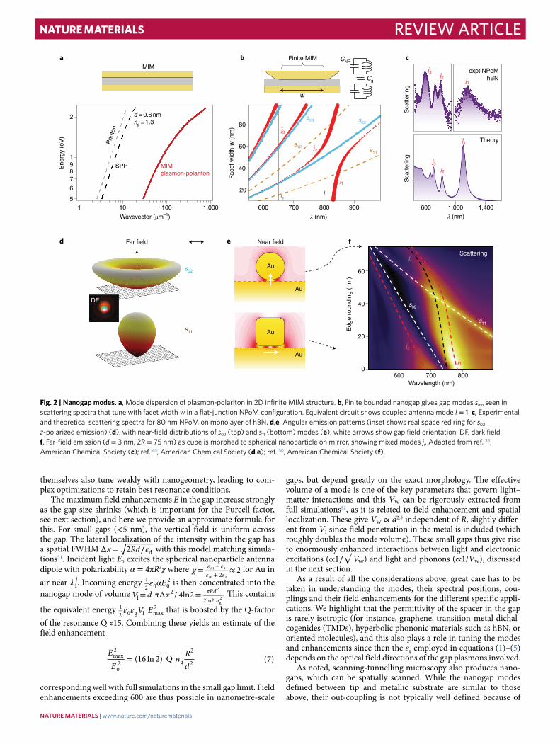
Basic concepts in plasmonic gap modesTo discuss the plasmonic gap modes, we first consider an infinite planar MIM multilayer35,36. For small gaps (d < 10 nm) of dielectric permittivity ε = ng g
2 between metallic walls (εm), the dispersion rela-tion of the lowest MIM modes can be written analytically35,37
ε ζ ε ε ζ∕ = = + + + − ∕∥k k n( ) 2 [1 1 ( ) ] (1)02
eff2
g g m
with
ζ ε ε= ∕ −k d( ) (2)0 m g2
which for typical nanogap parameters possess high wavevectors (k|| = 10–100 k0 with k0 = 2π/λ) and thus short effective wavelengths (Fig. 2a). These gap plasmon modes are robust against attenuation because when their in-plane wavevector increases with decreasing gap, the imaginary out-of-plane wavevector must also increase to ensure = +∥ ⊥k k k0
2 2 2, with a resulting field penetration depth
δε ε
=ℑ
=ℜ⊥
⊥kd1
m{ } 2 e{1 / } (3)g m
that correspondingly decreases38. As a result, the loss per unit length for MIM plasmons remains unchanged as the gap decreases (they travel slower, but retract from the metal, as similarly shown for monolayer metals such as graphene39).
This continuum of MIM gap modes is broken into discrete states by the shape of the particle’s facets, which localize the modes at the finite gap. A simple two-dimensional Fabry–Pérot resonator model given by the partial reflection of plasmons at the discontinuities of the MIM gap from each lower facet edge serves to capture the nature and symmetry of the modes sustained. For facet width w, the discrete wavelengths are then38,40
λα
λ λε
αε= π ≃ + ∞w n
w
d( ) (4)i
s
i ieff p
g
where αi are the zeros of the Bessel functions of the first kind (assuming here two-dimensional circular symmetry), and where a Drude metal permittivity ε ε λ λ= − ∕∞m
2p2 with dielectric back-
ground ε∞, and plasma wavelength λp is used (for Au λp≈148 nm). This set of modes spans the visible and near-infrared as the MIM facet or patch size w is varied (Fig. 2b). More generally, these tune also with the precise two-dimensional facet shape thus giving gap modes smn where indices m, n indicate the number of nodes in radial and azimuthal directions.41 With such small effective wavelengths,
these modes have very poor direct coupling efficiency to free space (of order 10–4).
However, the gap modes are able to couple to plasmonic antenna modes that span the entire nanoparticle–substrate system (Figs. 1,2b), and this greatly increases their coupling. Antenna mode wavelengths can be estimated using simple circuit models, which assume quasi-static field response in such small sub-wave-length resonators42–44. These treat each individual nanocomponent as lumped LCR resonators (Fig. 2b), which are then capacitively coupled by the gap, Cg, to give the lowest antenna mode (l = 1)45
λ λ ε ε ε= + + ∕∞ C C2 4 (5)l1 p d d g NP
where εd is the permittivity of the dielectric medium in which the system is embedded, and the capacitance of the nanoparticle/structure is CNP (2πRε0 for a sphere of radius R, with corresponding expressions for cubes or plates). This formula works for patterned multilayers, dimers, nanopatches and nanoparticles on a surface46, using the appropriate Cg,NP, and scales with the height of the nano-particle because charges oscillate across the entire structure (Fig. 1). For dimers or spherical NPoMs45, ε ς= + ∕χC C R dln[1 ]g NP g with constants χ≈0.5, ϛ≈0.15 for the NPoM, giving characteristic redshifts with decreasing gap and increasing nanoparticle size:
λ λ ε ε ε ε ς∕ = + + + ∕χ∞ R d( ) 2 4 ln[1 ] (6)l
1 p2
d d g
The next order (l = 2) antenna mode is shifted to shorter wavelengths by a factor ~1.25, set by the charge distributions that give the gap capacitance. Coupling strengths from free space to the antenna mode follow as R3, as expected from quasistatic dipole coupling to the entire nanoparticle volume46.
Antenna modes l with the correct symmetry can couple to spe-cific MIM gap plasmons smn, typically yielding strong anticrossings (Fig. 2b) and mixed smn + l = jn modes. It is around these anticross-ings between λl and λmn
s that light is most efficiently coupled into the nanogaps40 (Fig. 2c). However, the antenna–nanogap coupling depends exquisitely on the shape of the facet edges, as well as the mode symmetries, since facet edge morphology on the scale of 1/k||≈1 nm controls how easily gap plasmon fields reach around to the upper surfaces of the NP where antenna modes are located. Similar considerations obtain for modes of the cube-on-mirror47, which depend also on facet edge shapes. In larger gaps (d> 5 nm) MIM cavity nanogap modes with odd m (such as s11), which sup-port in-plane optical fields are found in the near-infrared (NIR); however, for smaller gaps these rapidly tune further into the infra-red (λ s
11 > 1 μm). By contrast, modes with even m possess strongest vertical (perpendicular) optical fields in the gap (s02) and remain in the visible–NIR even for the smallest gaps. Gap modes that do not mix with the antenna modes form dark modes48.
Different dipole-type emission patterns (Fig. 2d) arise from the different field orientations in the nanogap (Fig. 2e). In-plane modes present for larger gaps radiate normal to the substrate (85% collected by NA 0.9). By contrast, vertically polarized gap modes radiate symmetrically at high angles, θ θ∝ ∣ + ∣I r( ) 1 sinp
2 2 (where rp(θ) is the Fresnel factor for p-polarized light), giving maximum emission at ~60° in a full width at half maximum (FWHM) of 10° (with 55% thus collected by an objective with numerical aperture (NA) of 0.9), which is radially polarized and focusses to a real-space ring (Fig. 2d, inset). For real facets that are asymmetrically shaped, more complex polarization-dependent scattering spectra are observed, involving several split modes41,49. The different mode tuning with facet size can be seen by morphing a spherical NP into a nanocube50 of the same height (Fig. 2f), showing how the antenna mode crosses the in-plane field mode s11 (different symmetry), while anticrossing the vertical field mode s02. The antenna modes
Free space Antenna
~100 nm
Za
~100 nm
Z0 = 377 Ωλeff
Z Zc Zp
~1 nm ~ 0.1nm
Nanocavity Picocavity
+ + +
+ + +
– – –
– – –
Fig. 1 | impedance matched coupling of light from free space to atomic scale. Schematic of cascade of effective wavelength scales between free-space photons, coupled via antennas into nanogap modes, which can then couple to atomic-scale protrusions (‘picocavities’).
NAtuRE MAtERiAlS | www.nature.com/naturematerials
Review ARticleNatUre Materials
themselves also tune weakly with nanogeometry, leading to com-plex optimizations to retain best resonance conditions.
The maximum field enhancements E in the gap increase strongly as the gap size shrinks (which is important for the Purcell factor, see next section), and here we provide an approximate formula for this. For small gaps (<5 nm), the vertical field is uniform across the gap. The lateral localization of the intensity within the gap has a spatial FWHM εΔ = ∕x Rd2 d with this model matching simula-tions51. Incident light E0 excites the spherical nanoparticle antenna dipole with polarizability α = 4πR3χ where χ = ≈ε ε
ε ε−
+2
2m s
m s for Au in
air near λ l1. Incoming energy ε αE1
2 0 02 is then concentrated into the
nanogap mode of volume = πΔ = πV d x / 4ln2 RdnI
22ln2
2
g2. This contains
the equivalent energy ε ε V E12 0 g I max
2 that is boosted by the Q-factor of the resonance Q≈15. Combining these yields an estimate of the field enhancement
=EE
n Rd
(16 ln 2) Q (7)max2
02 g
2
2
corresponding well with full simulations in the small gap limit. Field enhancements exceeding 600 are thus possible in nanometre-scale
gaps, but depend greatly on the exact morphology. The effective volume of a mode is one of the key parameters that govern light–matter interactions and this VW can be rigorously extracted from full simulations52, as it is related to field enhancement and spatial localization. These give VW ∝ d2.5 independent of R, slightly differ-ent from VI since field penetration in the metal is included (which roughly doubles the mode volume). These small gaps thus give rise to enormously enhanced interactions between light and electronic excitations (∝ ∕√ V1 W) and light and phonons (∝1/VW), discussed in the next section.
As a result of all the considerations above, great care has to be taken in understanding the modes, their spectral positions, cou-plings and their field enhancements for the different specific appli-cations. We highlight that the permittivity of the spacer in the gap is rarely isotropic (for instance, graphene, transition-metal dichal-cogenides (TMDs), hyperbolic phononic materials such as hBN, or oriented molecules), and this also plays a role in tuning the modes and enhancements since then the εg employed in equations (1)–(5) depends on the optical field directions of the gap plasmons involved.
As noted, scanning-tunnelling microscopy also produces nano-gaps, which can be spatially scanned. While the nanogap modes defined between tip and metallic substrate are similar to those above, their out-coupling is not typically well defined because of
MIM
Sca
tterin
gS
catte
ring
Far field
Finite MIM
w
CNP
Cg
d = 0.6 nmng = 1.3
SPP MIMplasmon-polariton
Ene
rgy
(eV
)
Face
t wid
th w
(nm
)
280
60
40
40
Au
Au
0
20
60
20
Pho
ton
1
1 10 100 1,000 600
600 700 800Wavelength (nm)
Edg
e ro
undi
ng (
nm)
700 800
λ (nm) λ (nm)
900
987
6
5
Scattering
600 1,000 1,400
expt NPoMhBN
Theory
a
d Near field
s02
s02
s11
j2
j1
j1
j1
j2
j2
j3
j3
j2
j1
l1l2
s03 s02
s12s11
j3
l1
s11
e f
b c
Wavevector (μm–1)
DF
Au
Au
Fig. 2 | Nanogap modes. a, Mode dispersion of plasmon-polariton in 2D infinite MIM structure. b, Finite bounded nanogap gives gap modes smn seen in scattering spectra that tune with facet width w in a flat-junction NPoM configuration. Equivalent circuit shows coupled antenna mode l = 1. c, Experimental and theoretical scattering spectra for 80 nm NPoM on monolayer of hBN. d,e, Angular emission patterns (inset shows real space red ring for s02 z-polarized emission) (d), with near-field distributions of s02 (top) and s11 (bottom) modes (e); white arrows show gap field orientation. DF, dark field. f, Far-field emission (d = 3 nm, 2R = 75 nm) as cube is morphed to spherical nanoparticle on mirror, showing mixed modes ji. Adapted from ref. 38, American Chemical Society (c); ref. 63, American Chemical Society (d,e); ref. 50, American Chemical Society (f).
NAtuRE MAtERiAlS | www.nature.com/naturematerials

Review ARticle NatUre Materials
the lack of antenna modes. This can be ameliorated by shaping a neck on the tip53, using grating coupling54, coupling directly in the near-field to polariton modes34, or from the random metallic grain structure on the end of typical tips (hence the occasional ‘magic tips’ found).
Remarkably, additional confinement can be provided by individ-ual atomic protrusions into the gap. Time-dependent density-func-tional theory (TDDFT) for small nanoparticles confirms31,55,56 that even single atoms can provide up to fivefold further local electro-magnetic enhancement (on top of the plasmonic background field) leading to local fields more than a thousand times the incident field (Fig. 1). Intriguingly, classical electromagnetic calculations give very similar results, with protrusions of aspect ratio a=cos ϕ leading to extra enhancements ϕ ϕ ϕ= ∕ − ∕ ≃ + . + .E a asin (1 tan ) 1 1 7 0 3pico
2 2, of order ~3 for single-atom protrusions57. This effect is akin to the lightning rod effect, which is thus found to operate on the atomic scale, and produces cavity volumes VW<1 nm3 that are thus termed picocavities, and recently shown experimentally to be induced by optical irradiation31,58.
light–matter electronic interactions in nanogapsEmitters placed in the enhanced fields of such ultrathin metallic junctions experience modified absorption and emission rates, quan-tum efficiencies and radiation patterns, which can lead to strong coupling. A wide variety of materials can be integrated, including quantum dots59,60, mono- and few-layer TMDs61,62, and fluorescent dyes63,64 (Fig. 3a). The nanoscale spatial position of the emitter and orientation of its dipole moment is crucially important since the local fields of nanogap structures can vary significantly across a few nanometres and couple preferentially to one orientation of the dipole (p). To achieve this level of control, precision methods such as DNA origami can selectively position dye molecules (DNAo:dye)65 or barrel-shaped non-fluorescing molecules such as cucurbit[n]urils (CB[n]s) can be used to orient dye molecules of interest (CB:dye)66.
An important question that arises for emitters in close proxim-ity to plasmonic structures is whether the fluorescence is increased due to the high local field intensity or decreased due to non-radi-ative decay channels introduced by the metal. Large fluorescence enhancements of emitters coupled to plasmonic nanogap structures are observed67 (in some cases exceeding 30,000-fold63); however, quenching and reduced fluorescence have also been reported. Both scenarios indeed occur in seemingly similar structures, as the radia-tive and non-radiative decay rates depend intricately on the geom-etry and dimensions of the nanogap structure, the placement and initial quantum yield of emitters within it, and excitation condi-tions. Fluorescence changes arise from modified radiative quantum yields (QY; the probability that relaxation results in an emitted pho-ton), and altered efficiencies of excitation (γex) and collection (η) due to the antenna behaviour of plasmonic structures. Additionally, for high excitation powers at or near saturation, enhanced spon-taneous emission rates (γsp) enable the emitter to be re-excited after a shorter amount of time, also contributing to fluorescence enhancement. The fluorescence observed from an emitter coupled to a plasmonic structure compared to a control sample (denoted by superscript 0) is enhanced by a factor γ γ= ∕EF tot tot
0 (where γtot = ηγexγspQY), and the contribution from the increase in γsp should only be considered for excitation at or near saturation. The enhancement in excitation rate arises from γ ∝ ∣ ⋅ ∣p Eex
2 for E at the emitter’s posi-tion and transition frequency. If the QY is initially close to 100% it can only be decreased, but for emitters with lower QY such as infrared emitters68 and certain molecules, the QY can be increased significantly. Observation of fluorescence enhancement should thus not be attributed to either enhanced QY or enhanced spontaneous emission alone. Rather, a careful analysis is required of the interplay between the multiple contributing factors.
Tailoring the spontaneous emission rate of emitters by embed-ding them inside cavities offers the promise of ultrafast low-power light sources, modulators and single photon sources. The (intrinsic) dipole moment and controllable electromagnetic environment of an emitter determines its spontaneous emission rate, γ ρ∝ ∣ ∣psp
2 , where ρ is the local density of electromagnetic states at the position and frequency of the emitter, which can be obtained from Green’s func-tion approaches69–71. This electromagnetic environment is modified by high-quality-factor dielectric cavities or plasmonic structures with ultrasmall mode volumes as discussed here. An emitter then experiences an increased spontaneous decay rate compared to free space, with the ratio γ γ= ∕FP sp sp
0 known as the Purcell factor. The spontaneous decay rate, γsp = γr + γnr, has contributions from both radiative decay, γr, and non-radiative decay, γnr, which includes gen-eration of surface or localized modes and thermal dissipation. As the non-radiative decay rates can be significant for plasmonic struc-tures, the enhancement in radiative rate γ γ∕r r
0 where γr = γspQY is often of greater interest72, which requires fluorescence lifetime mea-surements and careful analysis to properly extract.
Balancing the trade-off between high field enhancements and non-radiative decay allows the observation of large radiative-rate enhancements ~1,000 for dye molecules embedded in a 10-nm gap between a metal film and silver nanocubes or nanowires73 or within a NPoM formed by DNA origami65. This spontaneous emission rate depends strongly on sub-nm changes in gap size (Fig. 3b,c). Such large enhancements enable quantum dots with initial lifetime of ~10 ns to emit photons on ultrafast timescales of 10 ps (ref. 59).
So far, we considered the weak coupling regime. However, for emitters with large oscillator strengths embedded in plasmonic cavities, the strong coupling regime can be observed. This occurs because γr is now faster than plasmon decay, leading to revers-ible energy exchange between the emitter and cavity mode and the emergence of hybridized light–matter states. This can be real-ized for ensembles of many emitters such as molecular aggregates situated between gold disk dimers74. Recently, strong coupling was observed even at the single-emitter level by precisely orienting a single molecule in the 0.9-nm gap between a gold sphere and film using the guest–host chemistry of CB:dye already described. When the transition dipole moment of the molecule is favourably oriented with the gap plasmon, the scattering spectra split, indicating strong coupling (Fig. 3d). With the molecule oriented perpendicular to the gap plasmon mode, no such splitting is observed emphasizing the need for precise control of emitter placement and orientation.
Plasmon–phonon vibrational coupling and optomechanicsA significant application for nanocavity plasmonics is the chemical interrogation of small numbers of molecules or ultrathin materials in real time, since the extreme field enhancements boost surface-enhanced Raman signals (SERS, scaling as Emax
4) of the samples located in the gap, enabling localized detection and fingerprinting. Early work on SERS blinking, which was used to evidence single-molecule signatures, is likely to be enabled by plasmons trapped in crevices between nanoparticles11,75–77. Many nanostructures supporting nanocavity plasmons give such characteristic SERS; however, in most cases the signals are irreproducible from individual structure to structure, limiting their utility. Key requirements are to precisely define the optical field distributions, enhancements and orientations, as well as the capability to tether the molecules/layers of interest in specific positions and orientations. With suitable scaf-folding, gap plasmons offer this capability, given the understanding of the modes already mentioned.
Robust SERS signatures are obtained when the gap is precisely defined by crystalline inorganics (such as CdTe few-unit-cell plate-lets78) or self-assembled monolayers (SAMs) of short alkyl chain or aromatic thiols. In the case of biphenyl-4-thiol (BPT) spacers creating NPoMs with d = 1.3 ± 0.1 nm, the SERS spectra vary little
NAtuRE MAtERiAlS | www.nature.com/naturematerials

Review ARticleNatUre Materials
with time or between different NPoMs (Fig. 4a) and match well to DFT calculations. Such non-resonant molecules have no electronic resonances at the plasmon frequency, hence only virtual states are involved in the excitation of vibrations and molecular damage minimized. Typical SERS emission of 1,000 counts s–1 mW–1 for each vibrational line ν correspond well to Raman cross sections Rk ≈ 0.5 nm4 a.m.u.–1 (from DFT) and the vibrational mode coupling strength to plasmon mode ωmn of
νω
ε=
ℏg
RV8
(8)k mn0
g W
This gives total coupling =g g Nm0 for Nm~100 molecules inside
the gap plasmon mode volume, assuming that all the molecules experience the same coupling. Small nanocavities thus enhance the SERS, while the plasmon coupling is to a collective vibration within all the molecules or bonds in an inorganic spacer layer. Variations in SERS amplitude in different nanogaps typically arise from inhomo-geneity of the patch/nanoparticle sizes and (facet) shapes46.
For a uniform Raman-active layer in the gap, assuming both incoming and outgoing light remains on resonance, the SERS amplitude is thus predicted to scale as ∝ ∝ ∕S V E R dW max
4 4 3. When the resonance condition is not maintained, a weaker dependence is observed experimentally, S ∝ R3, related to the scaling of facetting with R (ref. 46).
For molecular spacers which are either looser-packed or incorporate solvated ions, transient but extremely strong SERS signals can be seen79. These can now be understood to arise from
the picocavities (see previous section), which provide sub-nm light confinement so that only single-molecule emission dominates over the rest of the molecules in the gap (the Epico
4 SERS scaling gives additional hundredfold enhancement). How the single Au atom–molecule interaction forces lead to and stabilize this single-molecule SERS is not yet fully understood.
Picocavities enable observation of single-molecule SERS sig-natures that evolve on millisecond–second timescales. For exam-ple, flexing of individual lipid molecules gives rise to continuous vibrational shifts to higher and lower energies of different bonds80 (Fig. 4b), which are correlated according to how far the bonds are from the flexing location81. By contrast, when redox-active molecules are incorporated in the gap, their charging digitally shifts their vibrational energies (Fig. 4c) enabling single-molecule chemistry to be observed82. Reliable observations in such constructs open up opportunities for understanding and controlling chemistry at the single-molecule level.
An additional feature in nanogaps is the connection between the coupling of molecular vibrations to light and the optomechanical Hamiltonian, which are isomorphic31,83,84. Since the coupling g > 10 meV in picocavities (due to sub-nm3 volumes in equation (8)), optomechanical effects can deliver considerable impacts on the Raman emission even in ambient conditions. Molecular optome-chanics is able to provide stronger and nonlinear Raman emission as well as shaking molecules intensely enough to break chemical bonds31,85. We note that TERS also appears to often operate in this picocavity regime20, implying new optomechanical investigations can be accessed, as well as accounting for many of the fleeting signals previously seen (though long TERS integration times tend to aggregate these effects).
a
b c d
QDs
Nor
mal
ized
inte
nsity
γ exQ
Y
ω0
ωp
Time (ns) Gap size d (nm)
2R (nm)
2R
E0
100
10–1
10
1
11 nm
8 nm
10–2
0 0 100
40
60
NP
10080
200
Sca
tterin
g in
tens
ity
20 40
CB:dye DNAo:dye Molecule TMD
d
15 nm
Control
5 nm
500 600 700 800
Wavelenght (nm)
Au
d
NPoM
k
ω+ω–
Ω~ 380meV
Fig. 3 | Emitters in nanocavities. a, Emitter types include quantum dots (QDs), dye molecules supported by CB or DNA scaffolds, organic molecules, and monolayer materials (graphene, TMDs, hBN). b, Emission intensity decay for dyes in high Purcell factor cube-on-mirror versus gap size. c, Radiative yield of a single emitter in the gap centre of a plasmonic gold nanoparticle-on-mirror as a function of gap size, comparing single NP and NPoM. d, Strong coupling for three emitters in NPoM of configuration c with d = 0.9 nm gap. Adapted from ref. 64, Springer Nature Ltd (b); ref. 70, American Chemical Society (c); and ref. 66, Springer Nature Ltd (d).
NAtuRE MAtERiAlS | www.nature.com/naturematerials

Review ARticle NatUre Materials
Conduction and bridging in nanogapsSo far we have considered non-conducting spacers; however, con-ductivity can also be controlled in such small gaps with promising applications in optical or electro-optic switching. The small nano-cavity optical volumes (<10 nm3) imply minimal energy require-ments for switching, reaching potentially <1 zJ when few molecules are involved.
Modelling facetted NPoMs, including conducting bridges of increasing width spanning the gap, shows abrupt tuning and recon-figuration of the nanogap modes86 (Fig. 5a,b). Extending the above Fabry–Pérot MIM model explains this, assuming a perturbed cavity length Lg = (w − t)/2 is defined by facet/patch diameter w and bridge diameter t. Resonant ‘groove’ modes of this perturbed cavity are obtained at the resonance conditions λ= ∕′L r 2rg . Here
φ= + π′r r / 2g , where r = 0, 1, 2, … is the groove cavity mode order and φg ~ π/2 is a phase factor accounting for the boundary condi-tions of the nanocavity (now bounded by the Au bridge opposite the open edge of the facet, Fig. 5a). The energy of these groove modes is derived by solving the MIM dispersion (equation (1)) with groove wavevector kr = 2π/λr, giving tuning of the modes (Fig. 5b, white dashed lines).
As previously discussed, strongly confined gap modes do not radiate directly, but only if they can mix with antenna modes. For an antenna mode λ l
1 at a wavelength near 700 nm (vertical dashed line, Fig. 5b), which is barely perturbed by the bridging, spectral positions of the hybrid modes are obtained from the eigenvalues of the coupled system (white lines). Fitting suitable coupling strengths reproduces the full simulations of light scattering in this configura-tion (colour map), with near-field distributions that evanescently decay within the bridge (Fig. 5a) as predicted in this simple model. Such anti-crossings are directly seen in NPoM experiments using molecular layer gap spacers that are soft enough that optical irra-diation can drive metallic nanowires between the two metal walls86.
The modes blueshift with thicker bridges because the groove cavity length Lg reduces, ejecting modes one by one from the gap86. The blueshifts and mode crossings thus allow conducting bridge diameters and locations to be determined. The model shows field enhancement in the gap is typically three times smaller in the crevice after the gap has closed, thus giving 1–2 orders of magnitude smaller SERS from shorted gaps.
Such nanowire bridging is technologically important because it forms the basis of one class of memristive or resistive-random-access-memory (RRAM) devices, under intense investigation. These form two-terminal non-volatile low-energy storage cells, in which an applied threshold voltage is sufficient to drive a conductive link from one contact to another, which can be disassembled with sufficient reverse voltage. A major issue in these RRAMs is their sporadic failure after >105 cycles, from unknown causes that are hard to image in electron microscopy. By integrating such devices as a patch antenna MIM (Fig. 5c), dark-field spectroscopy is capable of watching the real-time dynamics of the nanowire through their groove modes87. Further studies have utilized a waveguide configuration88, while DFT simulations confirm that such bridges can form through single-atom nanowires55. Optical characteriza-tion in such nanogaps offers a number of advantages over electron microscopy, including access to in situ non-destructive dynamics under ambient operation conditions, revealing contact morpholo-gies on the nanometre scale.
Even without metallic bridges, conductive spacers influence the MIM modes89. Using SAMs of identical thickness (calibrated using ellipsometry) but differing in their electronic transport (through only a single additional sulfur atom on each molecule, which turns on hybridization with the Au) gives 60-nm blueshifts of the NPoM coupled plasmon (Fig. 5d). In this case, instead of groove modes the imaginary contribution to the vertical gap polarizability is increased, which partly discharges the nanogap capacitor within each optical half-cycle. The LCR model accounts for this when the gap capacitance is shunted by gap resistance Rg and kinetic induc-tance Lg (Fig. 5d, inset). The blueshifted screened antenna mode wavelength is then given (in the limit of conductivities greater than the quantum conductance G0 = (13 kΩ)−1 by45
λ λ ε ω ω= ∕ + ∕= (1 4 ) (9)l lscreened
11 d L
2p2
with the inductive coupling ω = ∕ L C1L g s for plasma frequency ωp = 2πc/λp and unscreened antenna mode λ l
1 from equation (5). This arises from a self-inductance of nanowires forming the effective conductive channel, since the moving electrons have to drag their magnetic field lines with them, increasing their inertia. At optical
a Robust spacers b Flexing
10–2
10–1 101 103 105
10–4
10–6
10–8
100
102
Nm~ 100 Nm=1
I II III1
0.1
100
0
SE
RS
inte
nsity
(ar
b)
SE
RS
inte
nsity
Tim
e (s
)
c Charging d Pumped vibrations
40
0
Tim
e (s
)
1,000Raman shift (cm–1) Raman shift (cm–1) Raman shift (cm–1)
2,000 1,000 1,500 1,5001,5002,000
Stokes
Optomechanics
Linear
Laser intensity (µW µm–2)
Phaser threshold
Anti-Stokes
50 c
m–1
Fig. 4 | Nanogap vibrational spectroscopy for chemistry and molecular optomechanics. a, Robust nanogaps with <100 BPT molecules in a uniform molecular layer in the gap show strong reliable SERS spectra (shown here for 50 NPoMs). b, Single-molecule vibrational modes of lipids in the gap show spectral wandering of SERS in time due to their flexing. c, Redox of single methyl-viologen molecules gives jumps in the vibrational frequencies seen in the SERS spectra with time, as charges jump on and off the molecule (III, with increased conductivity in I washing out nuclear motion). d, Molecular optomechanics regime induces non-linear enhancements of first anti-Stokes (dashed), and then Stokes (solid line) with pump power. Adapted from ref. 115, American Chemical Society (a); ref. 80, Springer Nature Ltd (b); ref. 82, Springer Nature Ltd (c); and ref. 85, APS (d).
NAtuRE MAtERiAlS | www.nature.com/naturematerials

Review ARticleNatUre Materials
frequencies, current only travels in a nanometre-thick outer sheath (depth Λ compared to nanowire radius a) yielding ε ω~ ∕L f a( )g 0 p
2 where fill fraction f = π−1(1 + d/2Λ). Substituting this gives wave-length shifts from the conductive layer in small gaps of45
λ λ ε= −= a
R1 (10)l l
screened1
1 d
which blue-shifts linearly with increasing width of the conducting linker, as confirmed by detailed simulations89.
Another prominent effect arising from creating conductive channels across plasmonic gaps is the emergence of low-energy modes for sufficiently large values of conductance. These modes are associated with charge transfer across the gap, which completely screens capacitive gap modes, producing plasmonic oscillations that extend over the entire particle-substrate system. The conductance
threshold GCTP for such charge-transfer plasmons to appear at long wavelengths λCTP is given by89
λ=G c R
d2CTPCTP
2
which is larger than that needed for the initial screening of the gap plasmons derived in equation (10). The emergence of these charge-transfer plasmons has been identified in several exper-iments involving nanogaps in metallic dimers90, nanoshells91 and particle chains92–94.
When the gap is deeply sub-nm (d< 0.5 nm) quantum correc-tions become important, covered in a recent review95. In brief, two corrections can be understood from (a) the effect at optical fre-quencies of the relative position of the centroid of charge density of
'
a
d e
b c
20
2.5
2.0 800
600
0.1 1 10
900Local
β=1.0x10⁶ m s–1
β=3.0x10⁶ m s–1
β=1.0x10⁷ m s–1
1.5
1.0
0.5
0.0
0
40
600 700Wavelength (nm)
QM regime
Ag filament
Ag+
r0r1
l1
r2
800
600500 700Wavelength (nm) Distance (nm)
Laser
BPDT
BPT
Cg
Lg
Rg
1,585 cm–1
800
Brid
ge w
idth
(nm
)
Sca
ttere
d in
tens
ity (
10–3
)
Res
onan
ce (
nm)
Lg
w
Full cavity
Groove cavity
t
AuNP
AuNP surface
Ag electrode
SiO2 gap
Au electrode
700
Au
ITO
Fig. 5 | tuning nanocavities with conductivity. a,b, Effect of bridging across the nanogap for increasing bridge width (downwards) (a) is to shift and mix modes in the scattering spectra (80 nm NPoM, colours show simulated scattering, white dashed lines show groove modes r from model in main text) (b). c, Resistive-RAM memory devices where applied voltage induces a stable nanowire exhibit gap tuning. d, Molecular layers show conduction-induced blue-shifts in the NPoM scattering resonance for different molecules (here BPDT has lower resistance than BPT). e, Modification of coupled resonance when including increasing quantum and non-local effects (through the hydrodynamic factor β). Adapted from ref. 115, American Chemical Society (a); ref. 86, American Chemical Society (a,b); ref. 87, Wiley (c); and ref. 27, AAAS (e).
NAtuRE MAtERiAlS | www.nature.com/naturematerials

Review ARticle NatUre Materials
the electronic excited state (surface plasmon) at the surface of the Au96 (beyond the classical localization at the sharp boundary due to the wavefunctions of the confined states), and (b) the quantum tunnelling through the dielectric gap which produces a shunt resis-tance Rg with effect similar to that noted above. Both these reduce the charge stored at the metallic gap surfaces, thus blue-shifting the gap plasmon51 (Fig. 5e). Experimentally stabilizing such sub-nanometre gaps is difficult, with experiments using conducting nanotips51, molecular spacers19,95,97,98 or graphene monolayers28, among others.
Applications and new directionsSeveral techniques now produce well-controlled nanometre spacers over large areas, both by top-down (such as atomic layer) deposi-tion or bottom-up coatings such as SAMs. This opens up the capa-bility to create ‘metasurfaces’ with tailored electric and magnetic response. Even disordered arrays accessible by bottom-up deposi-tion can create above-centimetre-scale surfaces covered by particle-on-a-mirror structures (Fig. 6a). By optimizing the mean distance between the plasmonic elements and the gap size, the response of the surface can be impedance matched to free space, resulting in near-perfect absorption at the plasmon resonance wavelength99–101. Strongly enhanced absorption of light at particular frequencies over large areas is useful for hot-electron photodetectors102, non-band-gap-limited thermal detectors103, light harvesting, surface coatings and enhanced non-linear generation, among other possibilities.
Periodically tiling these gap elements mixes in a sharper lattice-mode response104. Fabricating these currently demands lithographic lateral patterning such as photolithography105, but enables pixels to be created composed of metasurfaces with different resonances (Fig. 6a). This enables simultaneous on-chip capture of spectral and spatial information for multi- or hyper-spectral imaging with the potential to span ultraviolet to infrared spectral regions using a single-material platform, since absorption arises from ‘struc-tural colour’ rather than depending on a material bandgap. Hybrid bottom-up and top-down fabrication approaches can also realize combinatorial plasmonic-colour printing where the intensity of each RGB-channel is controlled by varying the fill fraction or shape of nanoparticles on the surfaces105,106. This could find use for fade-free printing, friend or foe infrared images or ultrahigh-resolution printing. Key challenges to resolve are creating large-area films at low cost that may preclude conventional or even imprint lithogra-phies. Perhaps most promising are self-assembly approaches requir-ing nanoscale design but which are tolerant enough to variable gap and particle sizes. More difficult is the associated backplane elec-tronic control which has not yet been shown to be low energy or scalable enough. Other opportunities in this area include improved nanoscale designs that give stronger contrast and faster (Fig. 6a, τ) and wider colour tuning (λ).
Due to the high local field enhancements in the gap, a small change in the properties of the material in this region, such as index of refraction or thickness, results in a large change in plas-mon resonance, useful for real-time reconfigurable structures107–109 or sensing110. In this way large area sub-microsecond colour-chang-ing wallpapers111 (Fig. 6b) or individual optically triggered NPoM switching (Fig. 6c) deliver low-energy actuation and access novel nano-optomechanical devices112. The search for electrical tun-ing has recently intensified with electrical gating configurations utilized113,114. The sensitivity of the plasmon modes to conductiv-ity115,116 points to a new field of molecular optoelectronics, with particular interest for spin-gated and switchable molecular devices. To progress this area, switchable gap materials have to be shown to be fast (τ < 1 ns is feasible due to the small volumes VW), robust over thousands of cycles, as well as deliver low-energy performance. Integration into optical backplanes or fibre geometries is a key goal requiring suitable materials combination.
Extreme nano-optics enables chemical reactions at the molecu-lar scale to be studied and influenced, alongside functional surface (electro-)chemistry. Similarly, dynamic bio-sensing is envisaged—for instance, of individual protein-complex machineries. Nanogap assemblies are being exploited to create the ‘intelligent toilet’, capa-ble of routine low-cost personalized healthcare117. The nanogap geometry is also particularly suited for study of electrochemical processes in the direct vicinity of electrodes, by tracking dynami-cally both SERS and scattering during reactions118,119. This applica-tion space has been plagued by the difficulty of translating research excitement into market traction, as specific applications have not been sufficiently targeted for large-scale trials. Part of the problem is collecting enough data to prove medical utility, and issues such as reproducibility of plasmonic nanoparticle surfactant chemistries, shelf life, contaminants and consistency of quantitative performance are still to be understood in sufficient detail.
Plasmonic nanostructures are capable of emitting ‘hot electrons’ under irradiation120. Several recent experiments in nanogaps show these effects directly, via chemical reactions under TERS tips121,122, reversible redox of single molecules in NPoMs82, and free radical polymerization of monomers to coat inside nanogaps123 (Fig. 6d). The tunability of plasmon modes and electronics states opens enormous opportunities in studying chemistry at the nanoscale in these systems, with many unanswered questions about the nature of molecule–surface interactions, and the efficiency of hot-electron plasmochemistry120. While this area is promising, quantitative information is lacking and unsubstantiated claims abound. Most crucial is to explore a wider range of industrially relevant reactions, and compare against state-of-the-art-processes, including the full energy and materials sourcing costs. The fraction of hot electrons per incident photon (which depends on the field enhancement Emax), and their energy spread must be measured, requiring develop-ment of new experimental techniques.
When emitters are embedded in nanogaps, as discussed in the section ‘Light–matter electronic interactions in nanogaps’, their spontaneous emission rate can be sped up significantly. This can enable a host of ultrafast optoelectronic applications, potentially in the THz regime, from modulators to ultrafast LEDs and pho-todetectors for on-chip information processing or even free-space optical communications124. This also broadens the range of lumi-nescent materials of interest for practical applications since the intrinsic material properties become less important. New questions then emerge as to material stability and properties under extreme field enhancements and high pumping conditions. Applications for on-chip quantum information processing could also be imagined as ultrafast single-photon sources have been demonstrated using quantum dots in nanogaps60 (Fig. 6e), while spin-selectivity demon-strated for nitrogen–vacancy centres in diamond125 and enhanced spontaneous parametric downconversion126 may enable the cre-ation of entangled photon pairs from ultrathin layers of nonlinear material. Room-temperature quantum emitters of high efficiency η capable of being packaged and used (at least in research facili-ties) requires key advances in developing photostable molecules (or other constructs), as well as improved tunability to make indistin-guishable sources (‘≠’). Solid-state emitters such as rare-earth ions in ultrathin films may prove a valuable route to integrate with these plasmonic nanocavities.
Advances in deterministic nanoassembly using DNA origami now allow specific numbers and types of molecules to be precisely inserted within ±1 nm locations inside the gap65 (Fig. 6f). In this arena, materials science and molecular science merge into precision nanotechnology. This allows new investigations of the plasmonic-modified intermolecular interactions including their electronic and vibrational coherences. In addition the large field gradients can induce ‘picoforces’ capable of bending and moving molecules. This area is extremely promising, and a wide array of different constructs
NAtuRE MAtERiAlS | www.nature.com/naturematerials

Review ARticleNatUre Materials
can be conceived that open up fundamental fields; however, appli-cations require much more photostable constructs, possibly using biomimetic redox strategies to avoid photobleaching steps.
With extreme optical confinement comes the capability to observe the motion of single metal atoms, which is induced by opti-cal irradiation of the gap modes31. This explains many observations in plasmonics over the years, such as the slow degradation of SERS properties at room temperature (caused by thermal excitation over the ~0.8 eV barrier for adatom site hopping). Irradiation moves gold or silver atoms86; however, its mechanism is not yet well understood, with both optical gradient forces at the single-atom level (‘picotwee-zers’) and non-equilibrium thermal and potential gradients being plausible candidates. Controllable single-atom optical switches are thus an exciting prospect for this new field of extreme nano-optics.
Received: 2 May 2018; Accepted: 16 January 2019; Published: xx xx xxxx
References 1. Ritchie, R. H. Plasma losses by fast electrons in thin films. Phys. Rev. 106,
874–881 (1957). 2. Krenn, J. R. et al. Squeezing the optical near-field zone by plasmon
coupling of metallic nanoparticles. Phys. Rev. Lett. 82, 2590–2593 (1999).
3. Krenn, J. R. et al. Direct observation of localized surface plasmon coupling. Phys. Rev. B 60, 5029–5033 (1999).
4. Ditlbacher, H., Krenn, J. R., Schider, G., Leitner, A. & Aussenegg, F. R. Two-dimensional optics with surface plasmon polaritons. Appl. Phys. Lett. 81, 1762–1764 (2002).
5. Maier, S. A. et al. Local detection of electromagnetic energy transport below the diffraction limit in metal nanoparticle plasmon waveguides. Nat. Mater. 2, 229–232 (2003).
6. Gramotnev, D. K. & Bozhevolnyi, S. I. Plasmonics beyond the diffraction limit. Nat. Photon. 4, 83–91 (2010).
7. Yang, W., Schatz, G. C. & Van Duyne, R. P. Discrete dipole approximation for calculating extinction and Raman intensities for small particles with arbitrary shapes. J. Chem. Phys. 103, 869–875 (1995).
8. Kottmann, J. P., Martin, O. J. F., Smith, D. R. & Schultz, S. Spectral response of plasmon resonant nanoparticles with a non-regular shape. Opt. Express 6, 213–219 (2000).
9. Mock, J. J., Barbic, M., Smith, D. R., Schultz, D. A. & Schultz, S. Shape effects in plasmon resonance of individual colloidal silver nanoparticles. J. Chem. Phys. 116, 6755–6759 (2002).
10. Kelly, K. L., Coronado, E., Zhao, L. L. & Schatz, G. C. The optical properties of metal nanoparticles: the influence of size, shape, and dielectric environment. J. Phys. Chem. B 107, 668–677 (2003).
11. Xu, H., Bjerneld, E. J., Käll, M. & Börjesson, L. Spectroscopy of single hemoglobin molecules by surface enhanced Raman scattering. Phys. Rev. Lett. 83, 4357–4360 (1999).
12. Kottmann, J. P. & Martin, O. J. F. Plasmon resonant coupling in metallic nanowires. Opt. Express 8, 655–663 (2001).
τ
τ
λ
λ
η
≠
λ
Con
tras
tG
amut
Integration
Spe
edS
tabi
lity
Energy efficiency
Tolerance Scale-up Robust
Precision molecular assemblies
Activemetasurfaces
1 mm
New gap materials
Nano-switchingHot-electron
plasmo-chemistry
Quantum emitters
1
0–40
50nm
0 40
Tuning:
Yield Utility
Photostability
Integration
Photostability
VW
VW
Emax
g (2)
Emax
fa
b
c d
e
200nm500nm
40 nm
Fig. 6 | Exploitation of nanocavities for new devices: molecular spintronics, thermo-optics, electro-optics. a,b, Colour-changing metasurfaces and wallpapers: tuning thin-film scattered colours. c, Low-energy optical switching of single NPoM. d, Hot-electron plasmo-chemistry dynamically grows polymer coatings. e, Room temperature quantum emitters. f, Precision molecular assembly: tuning molecular interactions, coherence and forces. Key demands for these applications around the outside, together with figures of merit (circled in yellow). Adapted from ref. 99, Wiley (a, left); ref. 105, Wiley (a, right); ref. 112, Wiley (c); ref. 123, American Chemical Society (d); ref. 60, American Chemical Society (e); and ref. 65, American Chemical Society (e).
NAtuRE MAtERiAlS | www.nature.com/naturematerials

Review ARticle NatUre Materials
13. Hao, E. & Schatz, G. C. Electromagnetic fields around silver nanoparticles and dimers. J. Chem. Phys. 120, 357–366 (2004).
14. Ghosh, S. K. & Pal, T. Interparticle coupling effect on the surface plasmon resonance of gold nanoparticles: from theory to applications. Chem. Rev. 107, 4797–4862 (2007).
15. Romero, I., Aizpurua, J., Bryant, G. W. & García De Abajo, F. J. Plasmons in nearly touching metallic nanoparticles: singular response in the limit of touching dimers. Opt. Express 14, 9988 (2006).
16. Koh, A. L., Fernández-Domínguez, A. I., McComb, D. W., Maier, S. A. & Yang, J. K. W. High-resolution mapping of electron-beam-excited plasmon modes in lithographically defined gold nanostructures. Nano Lett. 11, 1323–1330 (2011).
17. Lévêque, G. & Martin, O. J. F. Optical interactions in a plasmonic particle coupled to a metallic film. Opt. Express 14, 9971–9981 (2006).
18. Nordlander, P. & Le, F. Plasmonic structure and electromagnetic field enhancements in the metallic nanoparticle-film system. Appl. Phys. B 84, 35–41 (2006).
19. Kern, J. et al. Atomic-scale confinement of resonant optical fields. Nano Lett. 12, 5504–5509 (2012).
20. Zhang, R. et al. Chemical mapping of a single molecule by plasmon-enhanced Raman scattering. Nature 498, 82–86 (2013).
21. Zhang, Y. et al. Sub-nanometre control of the coherent interaction between a single molecule and a plasmonic nanocavity. Nat. Commun. 8, 15225 (2017).
22. Dathe, A., Ziegler, M., Hübner, U., Fritzsche, W. & Stranik, O. Electrically excited plasmonic nanoruler for biomolecule detection. Nano Lett. 16, 5728–5736 (2016).
23. Tuniz, A. & Schmidt, M. A. Interfacing optical fibers with plasmonic nanoconcentrators. Nanophotonics 7, 1279–1298 (2018).
24. Kuttge, M., Garcia de Abajo, F. J. & Polman, A. Ultrasmall mode volume plasmonic nanodisk resonators. Nano Lett. 10, 1537–1541 (2010).
25. Hu, M., Ghoshal, A., Marquez, M. & Kik, P. G. Single particle spectroscopy study of metal-film-induced tuning of silver nanoparticle plasmon resonances. J. Phys. Chem. C 114, 7509–7514 (2010).
26. Mock, J. J. et al. Distance-dependent plasmon resonant coupling between a gold nanoparticle and gold film. Nano Lett. 8, 2245–2252 (2008).
27. Ciraci, C. et al. Probing the ultimate limits of plasmonic enhancement. Science 337, 1072–1074 (2012).
28. Mertens, J. et al. Controlling subnanometer gaps in plasmonic dimers using graphene. Nano Lett. 13, 5033–5038 (2013).
29. Shvets, G. Photonic approach to making a material with a negative index of refraction. Phys. Rev. B 67, 035109 (2003).
30. Dionne, J. A., Sweatlock, L. A., Atwater, H. A. & Polman, A. Plasmon slot waveguides: towards chip-scale propagation with subwavelength-scale localization. Phys. Rev. B 73, 035407 (2006).
31. Benz, F. et al. Single-molecule optomechanics in “picocavities”. Science 354, 726–729 (2016).
32. Lee, K. F. Principles of Antenna Theory. (Wiley, Hoboken, 1984). 33. Parzefall, M. et al. Antenna-coupled photon emission from hexagonal
boron nitride tunnel junctions. Nat. Nanotechnol. 10, 1058–1063 (2015). 34. Du, W., Wang, T., Chu, H.-S. & Nijhuis, C. A. Highly efficient on-chip
direct electronic–plasmonic transducers. Nat. Photon. 11, 623–627 (2017). 35. Bozhevolnyi, S. I. & Søndergaard, T. General properties of slow-plasmon resonant
nanostructures: nano-antennas and resonators. Opt. Express 15, 10869 (2007). 36. Zayats, A. V., Smolyaninov, I. I. & Maradudin, A. A. Nano-optics of surface
plasmon polaritons. Phys. Rep. 408, 131–314 (2005). 37. Kuttge, M., Cai, W., García de Abajo, F. J. & Polman, A. Dispersion of
metal-insulator-metal plasmon polaritons probed by cathodoluminescence imaging spectroscopy. Phys. Rev. B 80, 033409 (2009).
38. Sigle, D. O. et al. Monitoring morphological changes in 2D monolayer semiconductors using atom-thick plasmonic nanocavities. ACS Nano 9, 825–830 (2015).
39. Alcaraz Iranzo, D. et al. Probing the ultimate plasmon confinement limits with a van der Waals heterostructure. Science 360, 291–295 (2018).
40. Tserkezis, C. et al. Hybridization of plasmonic antenna and cavity modes: extreme optics of nanoparticle-on-mirror nanogaps. Phys. Rev. A 92, 053811 (2015).
41. Kleemann, M.-E. et al. Revealing nanostructures through plasmon polarimetry. ACS Nano 11, 850–855 (2017).
42. Engheta, N., Salandrino, A. & Alù, A. Circuit elements at optical frequencies: nanoinductors, nanocapacitors, and nanoresistors. Phys. Rev. Lett. 95, 095504 (2005).
43. Liu, N. et al. Individual nanoantennas loaded with three-dimensional optical nanocircuits. Nano Lett. 13, 142–147 (2013).
44. Greffet, J.-J., Laroche, M. & Marquier, F. Impedance of a nanoantenna and a single quantum emitter. Phys. Rev. Lett. 105, 117701 (2010).
45. Benz, F. et al. Generalized circuit model for coupled plasmonic systems. Opt. Express 23, 33255 (2015).
46. Benz, F. et al. SERS of individual nanoparticles on a mirror: size does matter, but so does shape. J. Phys. Chem. Lett. 7, 2264–2269 (2016).
47. Bowen, P. T. & Smith, D. R. Coupled-mode theory for film-coupled plasmonic nanocubes. Phys. Rev. B 90, 195402 (2014).
48. Esteban, R. et al. The morphology of narrow gaps modifies the plasmonic response. ACS Photon. 2, 295–305 (2015).
49. Li, R.-Q., Hernángomez-Pérez, D., García-Vidal, F. J. & Fernández-Domínguez, A. I. Transformation optics approach to plasmon-exciton strong coupling in nanocavities. Phys. Rev. Lett. 117, 107401 (2016).
50. Chikkaraddy, R. et al. How ultranarrow gap symmetries control plasmonic nanocavity modes: from cubes to spheres in the nanoparticle-on-mirror. ACS Photon. 4, 469–475 (2017).
51. Savage, K. J. et al. Revealing the quantum regime in tunnelling plasmonics. Nature 491, 574–577 (2012).
52. Sauvan, C., Hugonin, J. P., Maksymov, I. S. & Lalanne, P. Theory of the spontaneous optical emission of nanosize photonic and plasmon resonators. Phys. Rev. Lett. 110, 237401 (2013).
53. Sanders, A. et al. Understanding the plasmonics of nanostructured atomic force microscopy tips. Appl. Phys. Lett. 109, 109–112 (2016).
54. Ropers, C. et al. Grating-coupling of surface plasmons onto metallic tips: a nanoconfined light source. Nano Lett. 7, 2784–2788 (2007).
55. Marchesin, F., Koval, P., Barbry, M., Aizpurua, J. & Sánchez-Portal, D. Plasmonic response of metallic nanojunctions driven by single atom motion: quantum transport revealed in optics. ACS Photon. 3, 269–277 (2016).
56. Barbry, M. et al. Atomistic near-field nanoplasmonics: reaching atomic-scale resolution in nanooptics. Nano Lett. 15, 3410–3419 (2015).
57. Urbieta, M. et al. Atomic-scale lightning rod effect in plasmonic picocavities: a classical view to a quantum effect. ACS Nano 12, 585–595 (2018).
58. Carnegie, C. et al. Room-temperature optical picocavities below 1 nm accessing single-atom geometries. J. Phys. Chem. Lett. 9, 7146–7151 (2018).
59. Hoang, T. B. et al. Ultrafast spontaneous emission source using plasmonic nanoantennas. Nat. Commun. 6, 7788 (2015).
60. Hoang, T. B., Akselrod, G. M. & Mikkelsen, M. H. Ultrafast room-temperature single photon emission from quantum dots coupled to plasmonic nanocavities. Nano Lett. 16, 270–275 (2016).
61. Akselrod, G. M. et al. Leveraging nanocavity harmonics for control of optical processes in 2D semiconductors. Nano Lett. 15, 3578–3584 (2015).
62. Huang, J., Akselrod, G. M., Ming, T., Kong, J. & Mikkelsen, M. H. Tailored emission spectrum of 2D semiconductors using plasmonic nanocavities. ACS Photon. 5, 552–558 (2018).
63. Rose, A. et al. Control of radiative processes using tunable plasmonic nanopatch antennas. Nano Lett. 14, 4797–4802 (2014).
64. Akselrod, G. M. et al. Probing the mechanisms of large Purcell enhancement in plasmonic nanoantennas. Nat. Photon. 8, 835–840 (2014).
65. Chikkaraddy, R. et al. Mapping nanoscale hotspots with single-molecule emitters assembled into plasmonic nanocavities using DNA origami. Nano Lett. 18, 405–411 (2018).
66. Chikkaraddy, R. et al. Single-molecule strong coupling at room temperature in plasmonic nanocavities. Nature 535, 127–130 (2016).
67. Kinkhabwala, A. et al. Large single-molecule fluorescence enhancements produced by a bowtie nanoantenna. Nat. Photon. 3, 654–657 (2009).
68. Akselrod, G. M. et al. Efficient nanosecond photoluminescence from infrared PbS quantum dots coupled to plasmonic nanoantennas. ACS Photon. 3, 1741–1746 (2016).
69. Argyropoulos, C., Ciracì, C. & Smith, D. R. Enhanced optical bistability with film-coupled plasmonic nanocubes. Appl. Phys. Lett. 104, 63108 (2014).
70. Kongsuwan, N. et al. Suppressed quenching and strong-coupling of Purcell-enhanced single-molecule emission in plasmonic nanocavities. ACS Photon. 5, 186–191 (2018).
71. Anger, P., Bharadwaj, P. & Novotny, L. Enhancement and quenching of single-molecule fluorescence. Phys. Rev. Lett. 96, 113002 (2006).
72. Pelton, M. Modified spontaneous emission in nanophotonic structures. Nat. Photon. 9, 427–435 (2015).
73. Russell, K. J., Liu, T.-L., Cui, S. & Hu, E. L. Large spontaneous emission enhancement in plasmonic nanocavities. Nat. Photon. 6, 459–462 (2012).
74. Schlather, A. E., Large, N., Urban, A. S., Nordlander, P. & Halas, N. J. Near-field mediated plexcitonic coupling and giant Rabi splitting in individual metallic dimers. Nano Lett. 13, 3281–3286 (2013).
75. Kneipp, K. et al. Single molecule detection using surface-enhanced Raman scattering (SERS). Phys. Rev. Lett. 78, 1667–1670 (1997).
76. Nie, S. Probing single molecules and single nanoparticles by surface-enhanced Raman scattering. Science 275, 1102–1106 (1997).
77. Qian, X.-M. & Nie, S. M. Single-molecule and single-nanoparticle SERS: from fundamental mechanisms to biomedical applications. Chem. Soc. Rev. 37, 912 (2008).
78. Sigle, D. O., Hugall, J. T., Ithurria, S., Dubertret, B. & Baumberg, J. J. Probing confined phonon modes in individual cdse nanoplatelets using surface-enhanced Raman scattering. Phys. Rev. Lett. 113, 087402 (2014).
79. Weiss, A. & Haran, G. Time-dependent single-molecule Raman scattering as a probe of surface dynamics. J. Phys. Chem. B 105, 12348–12354 (2001).
NAtuRE MAtERiAlS | www.nature.com/naturematerials
Review ARticleNatUre Materials
80. Taylor, R. W. et al. Watching individual molecules flex within lipid membranes using SERS. Sci. Rep. 4, 5940 (2015).
81. Sonntag, M. D., Chulhai, D., Seideman, T., Jensen, L. & Van Duyne, R. P. The origin of relative intensity fluctuations in single-molecule tip-enhanced Raman spectroscopy. J. Am. Chem. Soc. 135, 17187–17192 (2013).
82. De Nijs, B. et al. Plasmonic tunnel junctions for single-molecule redox chemistry. Nat. Commun. 8, 994 (2017).
83. Schmidt, M. K., Esteban, R., Benz, F., Baumberg, J. J. & Aizpurua, J. Linking classical and molecular optomechanics descriptions of SERS. Faraday Discuss. 205, 31–65 (2017).
84. Roelli, P., Galland, C., Piro, N. & Kippenberg, T. J. Molecular cavity optomechanics as a theory of plasmon-enhanced Raman scattering. Nat. Nanotechnol. 11, 164–169 (2016).
85. Lombardi, A. et al. Pulsed molecular optomechanics in plasmonic nanocavities: from nonlinear vibrational instabilities to bond-breaking. Phys. Rev. X 8, 011016 (2018).
86. Mertens, J. et al. Tracking optical welding through groove modes in plasmonic nanocavities. Nano Lett. 16, 5605–5611 (2016).
87. Di Martino, G., Tappertzhofen, S., Hofmann, S. & Baumberg, J. Nanoscale plasmon-enhanced spectroscopy in memristive switches. Small 12, 1334–1341 (2016).
88. Emboras, A. et al. Nanoscale plasmonic memristor with optical readout functionality. Nano Lett. 13, 6151–6155 (2013).
89. Pérez-González, O. et al. Optical spectroscopy of conductive junctions in plasmonic cavities. Nano Lett. 10, 3090–3095 (2010).
90. Scholl, J. A. et al. Evolution of plasmonic metamolecule modes in the quantum tunneling regime. ACS Nano 10, 1346–1354 (2016).
91. Lin, L. et al. Nanooptics of plasmonic nanomatryoshkas: shrinking the size of a core–shell junction to subnanometer. Nano Lett. 15, 6419–6428 (2015).
92. Fontana, J. & Ratna, B. R. Highly tunable gold nanorod dimer resonances mediated through conductive junctions. Appl. Phys. Lett. 105, 011107 (2014).
93. Herrmann, L. O. et al. Threading plasmonic nanoparticle strings with light. Nat. Commun. 5, 4568 (2014).
94. Koya, A. N. & Lin, J. Charge transfer plasmons: recent theoretical and experimental developments. Appl. Phys. Rev. 4, 021104 (2017).
95. Zhu, W. & Crozier, K. B. Quantum mechanical limit to plasmonic enhancement as observed by surface-enhanced Raman scattering. Nat. Commun. 5, 5228 (2014).
96. Teperik, T. V., Nordlander, P., Aizpurua, J. & Borisov, A. G. Robust subnanometric plasmon ruler by rescaling of the nonlocal optical response. Phys. Rev. Lett. 110, 263901 (2013).
97. Zhu, W. et al. Quantum mechanical effects in plasmonic structures with subnanometre gaps. Nat. Commun. 7, 11495 (2016).
98. Readman, C. et al. Anomalously large spectral shifts near the quantum tunnelling limit in plasmonic rulers with subatomic resolution. Nano Lett. https://doi.org/10.1021/acs.nanolett.9b00199 (2019)
99. Akselrod, G. M. et al. Large-area metasurface perfect absorbers from visible to near-infrared. Adv. Mater. 27, 8028–8034 (2015).
100. Moreau, A. et al. Controlled-reflectance surfaces with film-coupled colloidal nanoantennas. Nature 492, 86–89 (2012).
101. Rozin, M. J., Rosen, D. A., Dill, T. J. & Tao, A. R. Colloidal metasurfaces displaying near-ideal and tunable light absorbance in the infrared. Nat. Commun. 6, 7325 (2015).
102. Brongersma, M. L., Halas, N. J. & Nordlander, P. Plasmon-induced hot carrier science and technology. Nat. Nanotechnol. 10, 25–34 (2015).
103. Mauser, K. W. et al. Resonant thermoelectric nanophotonics. Nat. Nanotechnol. 12, 770–775 (2017).
104. Bowen, P. T., Baron, A. & Smith, D. R. Effective-medium description of a metasurface composed of a periodic array of nanoantennas coupled to a metallic film. Phys. Rev. A 95, 033822 (2017).
105. Stewart, J. W., Akselrod, G. M., Smith, D. R. & Mikkelsen, M. H. Toward multispectral imaging with colloidal metasurface pixels. Adv. Mater. 29, 1602971 (2017).
106. Goh, X. M. et al. Three-dimensional plasmonic stereoscopic prints in full colour. Nat. Commun. 5, 5361 (2014).
107. Hoang, T. B. & Mikkelsen, M. H. Broad electrical tuning of plasmonic nanoantennas at visible frequencies. Appl. Phys. Lett. 108, 183107 (2016).
108. Wilson, W. M., Stewart, J. W. & Mikkelsen, M. H. Surpassing single line width active tuning with photochromic molecules coupled to plasmonic nanoantennas. Nano Lett. 18, 853–858 (2018).
109. Ding, T., Mertens, J., Sigle, D. O. & Baumberg, J. J. Capillary-force-assisted optical tuning of coupled plasmons. Adv. Mater. 27, 6457–6461 (2015).
110. Powell, A. W. et al. Plasmonic gas sensing using nanocube patch antennas. Adv. Opt. Mater. 4, 634–642 (2016).
111. Ding, T. et al. Fast dynamic color switching in temperature-responsive plasmonic films. Adv. Opt. Mater. 4, 877–882 (2016).
112. Cormier, S., Ding, T., Turek, V. & Baumberg, J. J. Actuating single nano-oscillators with light. Adv. Opt. Mater. 6, 1701281 (2018).
113. Holsteen, A. L., Raza, S., Fan, P., Kik, P. G. & Brongersma, M. L. Purcell effect for active tuning of light scattering from semiconductor optical antennas. Science 358, 1407–1410 (2017).
114. Liu, X. et al. Electrical tuning of a quantum plasmonic resonance. Nat. Nanotechnol. 12, 866–870 (2017).
115. Benz, F. et al. Nanooptics of molecular-shunted plasmonic nanojunctions. Nano Lett. 15, 669–674 (2015).
116. Tan, S. F. et al. Quantum plasmon resonances controlled by molecular tunnel junctions. Science 343, 1496–1499 (2014).
117. Kasera, S., Herrmann, L. O., Barrio, J., del, Baumberg, J. J. & Scherman, O. A. Quantitative multiplexing with nano-self-assemblies in SERS. Sci. Rep. 4, 6785 (2015).
118. Di Martino, G. et al. Tracking nanoelectrochemistry using individual plasmonic nanocavities. Nano Lett. 17, 4840–4845 (2017).
119. Hoener, B. S. et al. Spectral response of plasmonic gold nanoparticles to capacitive charging: morphology effects. J. Phys. Chem. Lett. 8, 2681–2688 (2017).
120. Cortés, E. et al. Plasmonic hot electron transport drives nano-localized chemistry. Nat. Commun. 8, 14880 (2017).
121. Sun, M., Zhang, Z., Zheng, H. & Xu, H. In-situ plasmon-driven chemical reactions revealed by high vacuum tip-enhanced Raman spectroscopy. Sci. Rep. 2, 647 (2012).
122. van Schrojenstein Lantman, E. M., Deckert-Gaudig, T., Mank, A. J. G., Deckert, V. & Weckhuysen, B. M. Catalytic processes monitored at the nanoscale with tip-enhanced Raman spectroscopy. Nat. Nanotechnol. 7, 583–586 (2012).
123. Ding, T., Mertens, J., Lombardi, A., Scherman, O. A. & Baumberg, J. J. Light-directed tuning of plasmon resonances via plasmon-induced polymerization using hot electrons. ACS Photon. 4, 1453–1458 (2017).
124. Peyronel, T., Quirk, K. J., Wang, S. C. & Tiecke, T. G. Luminescent detector for free-space optical communication. Optica 3, 787–792 (2016).
125. Bogdanov, S. et al. Electron spin contrast of Purcell-enhanced nitrogen-vacancy ensembles in nanodiamonds. Phys. Rev. B 96, 035146 (2017).
126. Davoyan, A. R. & Atwater, H. A. Quantum nonlinear light emission in metamaterials: broadband Purcell enhancement of parametric downconversion. Optica 5, 608–611 (2018).
AcknowledgementsWe acknowledge support from UK EPSRC grants EP/G060649/1, EP/L027151/1, EP/G037221/1, EPSRC NanoDTC, ERC grant LINASS 320503, and FIS2016-80174-P from Spanish Ministry MINECO. M.H.M. acknowledges support from the Air Force Office of Scientific Research (AFOSR, grant no. FA9550‐15‐1‐0301) and the National Science Foundation (DMR-1454523). We appreciate extensive data and discussions on the mode scaling with A. Demetriadou, and enormous contributions from many members of our research groups over the past decade.
Author contributionsAll authors contributed equally to the preparation of this manuscript.
Competing interestsThe authors declare no competing interests.
Additional informationReprints and permissions information is available at www.nature.com/reprints.
Correspondence should be addressed to J.J.B.
Publisher’s note: Springer Nature remains neutral with regard to jurisdictional claims in published maps and institutional affiliations.
© Springer Nature Limited 2019
NAtuRE MAtERiAlS | www.nature.com/naturematerials