
Experimental Study of Stacked Rectangular Microstrip ... · microstrip antenna which is stacked one...
6
Engineering, 2010, 2, 85-90 doi:10.4236/eng.2010.22011 Published Online February 2010 (http://www.scirp.org/journal/eng). Copyright © 2010 SciRes. ENGINEERING Experimental Study of Stacked Rectangular Microstrip Antenna for Dual-Band Rajesh Kumar Vishwakarma 1 , Sanjay Tiwari 2 School of Studies in Electronics, Pt. Ravishankar Shukla University, Raipur, Chhattisgarh (C.G) E-mail: [email protected], [email protected] Received August 27, 2009; revised September 14, 2009; accepted September 20, 2009 Abstract A dual-band characteristic of stacked rectangular microstrip antenna is experimentally studied. It is a probe fed antenna for impedance matching with 50Ω coaxial cable. This antenna works well in the frequency range (2.86 to 4.63 GHz). It is basically a low cost, light weight medium gain antenna, which is used for mobile communication. The variations of the length and width (1mm) of the stacked rectangular patch antenna have been done. And it is found dual resonance with increasing lower resonance frequency and almost constant upper resonance frequency with increases of the length & width of rectangular microstrip antenna. The input impedance and VSWR, return loss have been measured with the help of Network analyzer. Keywords: Microstrip Antenna, Stacked Patch Antenna, Dual-Band Antenna, Network Analyzer, Bandwidth 1. Introduction The demand for application of microstrip antenna in various communication systems has been increasing rapidly due to its lightweight, low cost, small size, ease of integration with other microwave components [1–4]. Microstrip antenna gained in popularity and become a major research topic in both theoretically and experi- mentally. However one of main disadvantages of micro- strip antenna is their narrow band width. It is well known that the multilayer structure is useful method to improve these problems. The researcher have investigated their basic characteristics and extensive efforts have also been developed to design of electromagnetically coupled two layer elliptical microstrip stacked antenna [5], stacked square patch antenna for Bluetooth application [6] and analysis of stacked microstrip rectangular microstrip antenna [7]. Several methods have been presented in the last years to improve it , s such as: thicker substrate [8] reactive matching network [9], and stacked patches [10–12]. Microstrip patch antenna elements with a single feed are used in many popular for various radar and communication system such as synthetics aperture radar (SAR), dual-band, multi-band, mobile communication system and Global Positing Systems (GPS) [13]. It may be mentioned that the bandwidth can also be improved by stacking a parasitic patch on the fed patch [14]. Therefore in this present paper, we observed on an elec- tromagnetically stacked rectangular microstrip antenna with number of parasitic elements. By using two stacked patches with the wall at edges between the two patches, one can obtained enhance impedance bandwidth. Ex- perimental work is carried out to study the effect of stacking on various parameters of antenna. 2. Antenna Design Calculation The transmission line model is used to design rectangular microstrip antenna which is stacked one by one. Rectan- gular microstrip antenna (RMA) is designed by using following procedures. 2.1. Patch Width and Patch Length The first to design the patch is choosing a suitable di- electric substrate of suitable thickness. For rectangular microstrip antenna, the width W and the length L de- pends on the resonant frequency r f and the parameters of the substrate employed [1]. To design the rectangular patch width of the antenna is given by 2 1 2 1 2 r r ε f c W (1) where C= velocity of light W = width of the microstrip patch r = Dielectric constant of the substrate Length of the resonant element is given by
Transcript of Experimental Study of Stacked Rectangular Microstrip ... · microstrip antenna which is stacked one...

Engineering, 2010, 2, 85-90 doi:10.4236/eng.2010.22011 Published Online February 2010 (http://www.scirp.org/journal/eng).
Copyright © 2010 SciRes. ENGINEERING
Experimental Study of Stacked Rectangular Microstrip Antenna for Dual-Band
Rajesh Kumar Vishwakarma1, Sanjay Tiwari2
School of Studies in Electronics, Pt. Ravishankar Shukla University, Raipur, Chhattisgarh (C.G) E-mail: [email protected], [email protected]
Received August 27, 2009; revised September 14, 2009; accepted September 20, 2009
Abstract A dual-band characteristic of stacked rectangular microstrip antenna is experimentally studied. It is a probe fed antenna for impedance matching with 50Ω coaxial cable. This antenna works well in the frequency range (2.86 to 4.63 GHz). It is basically a low cost, light weight medium gain antenna, which is used for mobile communication. The variations of the length and width (1mm) of the stacked rectangular patch antenna have been done. And it is found dual resonance with increasing lower resonance frequency and almost constant upper resonance frequency with increases of the length & width of rectangular microstrip antenna. The input impedance and VSWR, return loss have been measured with the help of Network analyzer. Keywords: Microstrip Antenna, Stacked Patch Antenna, Dual-Band Antenna, Network Analyzer, Bandwidth 1. Introduction The demand for application of microstrip antenna in various communication systems has been increasing rapidly due to its lightweight, low cost, small size, ease of integration with other microwave components [1–4]. Microstrip antenna gained in popularity and become a major research topic in both theoretically and experi-mentally. However one of main disadvantages of micro-strip antenna is their narrow band width. It is well known that the multilayer structure is useful method to improve these problems. The researcher have investigated their basic characteristics and extensive efforts have also been developed to design of electromagnetically coupled two layer elliptical microstrip stacked antenna [5], stacked square patch antenna for Bluetooth application [6] and analysis of stacked microstrip rectangular microstrip antenna [7]. Several methods have been presented in the last years to improve it, s such as: thicker substrate [8] reactive matching network [9], and stacked patches [10–12]. Microstrip patch antenna elements with a single feed are used in many popular for various radar and communication system such as synthetics aperture radar (SAR), dual-band, multi-band, mobile communication system and Global Positing Systems (GPS) [13]. It may be mentioned that the bandwidth can also be improved by stacking a parasitic patch on the fed patch [14]. Therefore in this present paper, we observed on an elec-tromagnetically stacked rectangular microstrip antenna
with number of parasitic elements. By using two stacked patches with the wall at edges between the two patches, one can obtained enhance impedance bandwidth. Ex-perimental work is carried out to study the effect of stacking on various parameters of antenna.
2. Antenna Design Calculation
The transmission line model is used to design rectangular microstrip antenna which is stacked one by one. Rectan-gular microstrip antenna (RMA) is designed by using following procedures.
2.1. Patch Width and Patch Length
The first to design the patch is choosing a suitable di-electric substrate of suitable thickness. For rectangular microstrip antenna, the width W and the length L de-pends on the resonant frequency
rf and the parameters
of the substrate employed [1]. To design the rectangular patch width of the antenna is
given by
2
1
2
1
2
r
r
ε
f
cW (1)
where C= velocity of light W = width of the microstrip patch
r = Dielectric constant of the substrate Length of the
resonant element is given by
86 R. K. VISHWAKARMA ET AL.
lΔεf
cL
effr
22
(2)
where
eff = Effective dielectric constant of the substrate
l = Line extension
eff and can be expressed as l50
101
2
1
2
1.
rreff W
hεεε
258.0
3.0
813.0
262.0412.0
eff
eff
h
Wh
W
hl
where, h is the thickness of the substrate. The driven patches were designed to operate at a reso-
nant frequency of 3.0 GHz, their length and width were calculated to be L= 23.01mm and width W= 30.01mm respectively. The remaining five patches were designed with the differences of 1mm in the length and width with increasing mode. They are stacked in the manner shown in (Figure 1).
2.2. Feeding Design
The feeding point was designed for lower patch to match the (50 Ω) coaxial cable feed and the patch. The feeding point was fabricated along the length of the patch. The input conductance of the patch fed on the edge slot will be twice the conductance of one of the edge slots as suggested by Harrington and given by [15].
241
2
0
khWG
(3)
where 120 0
2
k 0 Wavelength of free
space So the input impedance of the patch is given by R1= 1/2G (Ω), where G is radiation conductance.
So the upper patch is parasitic and the lower patch is fed with a co axial probe at the position (X0, Y0) where X0=
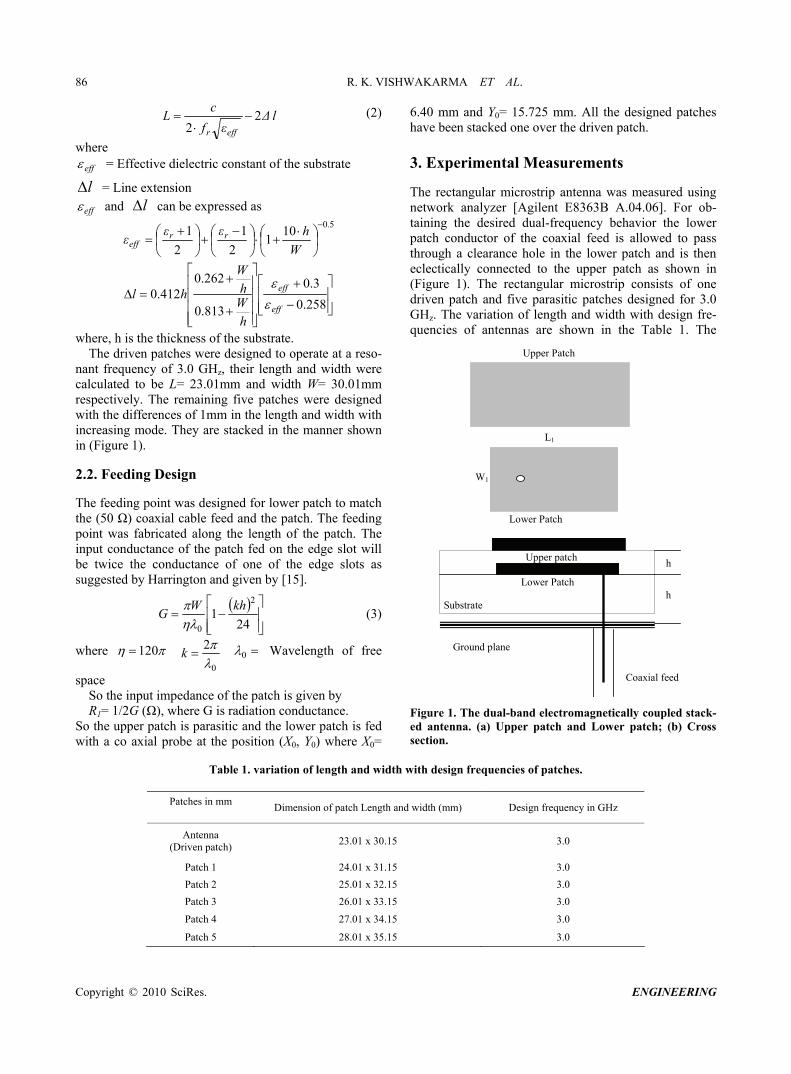
6.40 mm and Y0= 15.725 mm. All the designed patches have been stacked one over the driven patch. 3. Experimental Measurements
The rectangular microstrip antenna was measured using network analyzer [Agilent E8363B A.04.06]. For ob-taining the desired dual-frequency behavior the lower patch conductor of the coaxial feed is allowed to pass through a clearance hole in the lower patch and is then eclectically connected to the upper patch as shown in (Figure 1). The rectangular microstrip consists of one driven patch and five parasitic patches designed for 3.0 GHz. The variation of length and width with design fre-quencies of antennas are shown in the Table 1. The
Upper Patch
W1
Lower Patch
L1
h
h Lower Patch
Upper patch
Ground plane
Coaxial feed
Substrate
Figure 1. The dual-band electromagnetically coupled stack- ed antenna. (a) Upper patch and Lower patch; (b) Cross section.
Table 1. variation of length and width with design frequencies of patches.
Patches in mm
Dimension of patch Length and width (mm) Design frequency in GHz
Antenna (Driven patch)
23.01 x 30.15 3.0
Patch 1 24.01 x 31.15 3.0
Patch 2 25.01 x 32.15 3.0
Patch 3 26.01 x 33.15 3.0
Patch 4 27.01 x 34.15 3.0
Patch 5 28.01 x 35.15 3.0
Copyright © 2010 SciRes. ENGINEERING

R. K. VISHWAKARMA ET AL. 87
Table 2. Variation of upper and lower resonance frequencies and their ratio (f2/f1) with return loss in dB.
Patches in mm
Lower resonance frequency
f1 (GHz)
Upper resonance frequency
f2 (GHz)
Ratio of resonance frequencies f2 / f1 (GHz)
Return loss(dB) for f1 (GHz)
Return loss(dB) for f2 (GHz)
Patch 1 2.868 4.585 2.868 -9.99 -12.24 Patch 2 2.904 4.625 2.904 -11.85 -14.24 Patch 3 2.903 4.593 2.903 -10.89 -12.65 Patch 4 2.917 4.624 2.917 -13.26 -14.46 Patch 5 2.917 4.636 2.917 -13.80 -14.45
variation of upper and lower resonance frequencies and their ratio (f2/f1) with increasing patch length and width are shown in the Table 2. In order to study the perform-ance of the development rectangular microstrip antenna return loss, resonance frequencies and VSWR were measured experientially with different number of para-sitic antenna shown in the Table 2. The broad band width is achieved about 45% with the stacking of the antenna.
4. Design Parameters
The various design parameters of the antenna are as fol-lows:
Substrate material used Glass Epoxy Thickness of the dielectric substrate h = 1.59 mm
(a)
(b)
(c)
(d)
(e)
Figure 2. (a) Variations of input impedance with frequency for patch dimension 24.01x 31.15; (b) Variations of input impedance with frequency for patch dimension 25.01x 32.15; (c) Variations of input impedance with frequency for patch dimension 26.01x 33.15; (d) Variations of input impedance with frequency for patch dimension 27.01x 34.15; (e) Varia-tions of input impedance with frequency for patch dimen-sion 28.01x 35.15.
Copyright © 2010 SciRes. ENGINEERING

88 R. K. VISHWAKARMA ET AL.
(a)
(b)
(c)
(d)
(e)
Figure 3. (a) Variations of VSWR with frequency for patch dimension 24.01x 31.15; (b) Variations of VSWR with fre-quency for patch dimension 25.01x 32.15; (c) Variations of VSWR with frequency for patch dimension 26.01x 33.15; (d) Variations of VSWR with frequency for patch dimension 27.01x 34.15; (e) Variations of VSWR with frequency for patch dimension 28.01x 35.15.
Relative permittivity of the substrate r = 4. Design frequency f = 3.0 GHz Thickness of the patch t = 0.0018cm And designed values were calculated using the stan-
dard equations, which are given below. The width of the rectangular patch (Driven Patch) W1 = 30.15 mm.
The length of the rectangular patch (Driven Patch) L1 = 23.01 mm.
The variation of length of the patch (Parasitic Patch) L = 24.01 mm to 28.01 mm.
The variation of width length of the patch (Parasitic Patch) W = 31.15 mm to 35.15 mm.
5. Discussion of Results
1) The variation of input impedance with frequency for rectangular dimensions (Patch 1 to Patch 5) is shown in Figures 2(a) to 2(e). It is observed that stacked patch an-tenna shows dual resonance in which lower resonance frequency increases with increasing patch dimensions frequencies increase with increasing the patch dimensions.
2) The variation of VSWR with frequency for rectan-gular dimensions (Patch 1 to Patch 5) is shown in Fig-ures 3(a) to 3(e) It is observed that the value of VSWR corresponding to lower resonance frequency is decreases from 1.96 to 1.54 with increasing patch dimensions where as at the upper resonance frequency the value of VSWR is also decrease from 1.66 to 1.47.
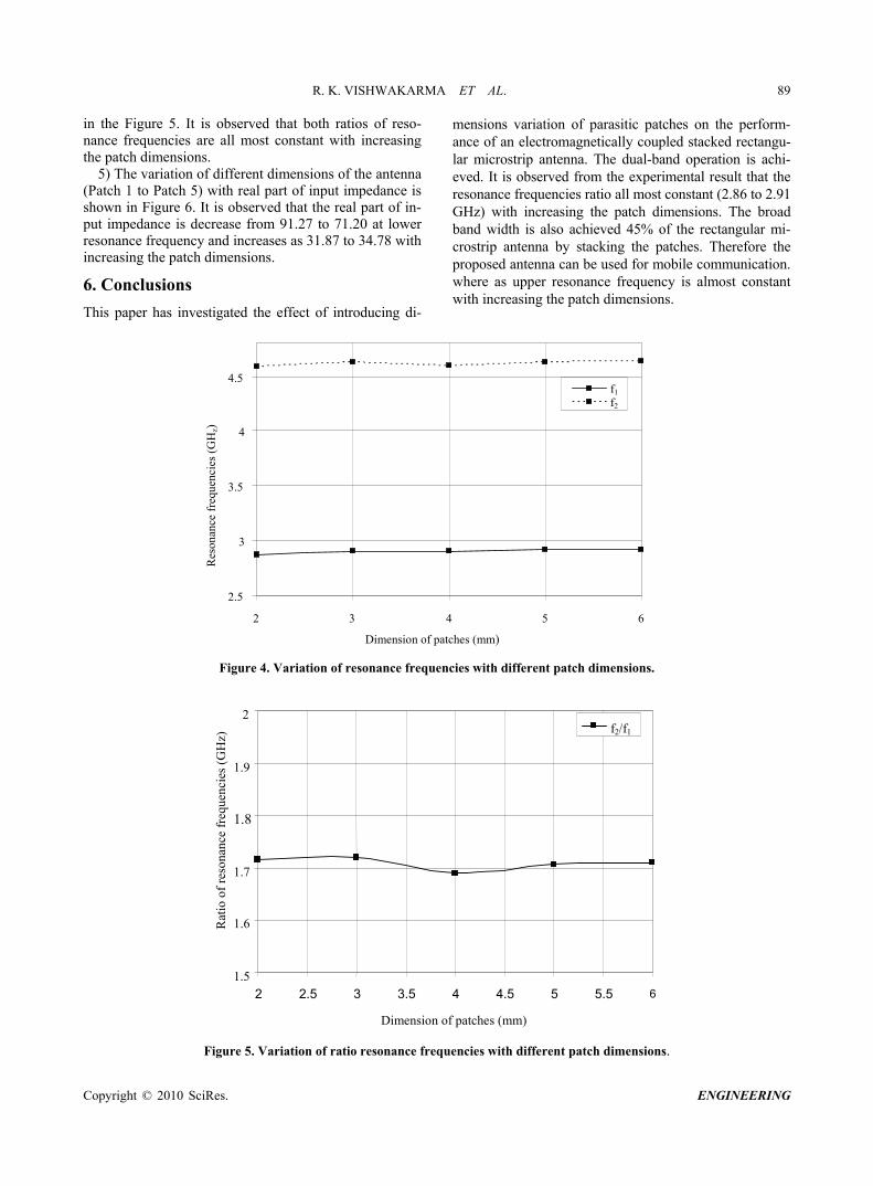
3) The variation of resonance frequencies with different dimensions of the antenna (Patch 1 to Patch 5) are shown in the Figure 4, It is observed that both resonance fre-quencies increase with increasing the patch dimensions.
4) The variation of resonance frequency ratio f2/f1 with dimensions of the antenna (Patch 1 to Patch 5) is shown
Copyright © 2010 SciRes. ENGINEERING
R. K. VISHWAKARMA ET AL. 89
Copyright © 2010 SciRes. ENGINEERING
in the Figure 5. It is observed that both ratios of reso-nance frequencies are all most constant with increasing the patch dimensions.
5) The variation of different dimensions of the antenna (Patch 1 to Patch 5) with real part of input impedance is shown in Figure 6. It is observed that the real part of in-put impedance is decrease from 91.27 to 71.20 at lower resonance frequency and increases as 31.87 to 34.78 with increasing the patch dimensions.
6. Conclusions
This paper has investigated the effect of introducing di-
mensions variation of parasitic patches on the perform-ance of an electromagnetically coupled stacked rectangu-lar microstrip antenna. The dual-band operation is achi- eved. It is observed from the experimental result that the resonance frequencies ratio all most constant (2.86 to 2.91 GHz) with increasing the patch dimensions. The broad band width is also achieved 45% of the rectangular mi-crostrip antenna by stacking the patches. Therefore the proposed antenna can be used for mobile communication. where as upper resonance frequency is almost constant with increasing the patch dimensions.
2.5
3
3.5
4
4.5
2 3 4 5
Dimension of patches (mm)
6
f1
f2
Res
onan
ce f
requ
enci
es (
GH
z)
Figure 4. Variation of resonance frequencies with different patch dimensions.
1.5
1.6
1.7
1.8
1.9
2
2 2.5 3 3.5 4 4.5 5 5.5 6
Dimension of patches (mm)
Rat
io o
f re
sona
nce
freq
uenc
ies
(GH
z)
f2/f1
Figure 5. Variation of ratio resonance frequencies with different patch dimensions.

90 R. K. VISHWAKARMA ET AL.
30
40
50
60
70
80
90
2 3 4 5 Dimension of patches (mm)
Rea
l par
t of
inpu
t im
peda
nce
(ohm
)
6
R_part (f1)
R_part (f2)
Figure 6. Variations of patch dimensions with real part of input impedance. 7. Acknowledgments The authors would like to thank Professors Arun Kumar and Shri R. K. Malaviya of the Space Application Centre, Indian Space Research Organization Ahmedabad, for providing the measurement facilities. 8. References
[1] J. l. BahI, and P. Bhartia, Microstrip Antennas, Dedham, MA, (USA) Artech House, 1980.
[2] J. R. James, P. S. Hall, and C. Wood, “Microstrip antenna theory and design” IEE Electromagnetic Wave, Series 12 London, U. K. Peter Peregrinus, 1981.
[3] K. C. Gupta, “Recent advance in microstrip antenna,” Microwave Journal, No. 27, pp. 50–67, 1984.
[4] S. A. Long and M. D. Walton, “A dual-frequency circu-lar-disc antenna,” IEEE Transactions on Antenna and Propagation USA, AP-27, pp. 270–273, 1979.
[5] R. L. Yadava and B. R. Vishvakarma, “Analysis of elec-tromagnetically coupled two-layer elliptical microstrip stacked antennas,” International Journal of Electronics, Vol. 87, No. 8, pp. 981–993, 2000.
[6] A. B. Nandgaonkar and S. B. Deosarkar, “Broadband stacked patch antenna for bluetooth applications,” Journal of Microwaves, Optoelectronics and Electromagnetic Application, Vol. 8, No. 1, pp. 1–5, 2009.
[7] I. K. Moussa and D. A. E. Mohamed and I. badran, “Analysis of stacked rectangular microstrip antenna,” 24th National Radio Science Conference, March 13-15, pp. 1–
10, 2007.
[8] W. Chen, K. F. Lee, and R. O. Lee, “Input impedance of coaxially fed rectangular microstrip antenna on electri-cally thick substrate,” Microwave optical Technology Letters, Vol. 6, No. 6, pp. 387–390, 1993.
[9] F. Pues and R. Van De Capelle, “An impedance matching technique for increasing the bandwidth of microstrip an-tenna,” IEEE Transactions on Antennas Propagation, Vol. 37, pp. 1345–1354, 1989.
[10] J. S. Dahel and K. F. Lee,“A dual-frequency stacked mi-crostrip antenna,” IEEE AP-S International Symposium Digest, pp. 308–30–11, 1982.
[11] K. F. Lee, K. Y. Ho, and J. S. Dahele, “Circular-disk mi-crostrip antenna with air gap”, IEEE Transactions on An-tenna (USA) and Propagation, AP-32, pp. 880–884, 1984.
[12] J. S. Dahele, K. F. Lee, and D. P. Wong, “Dual frequency stacked annular ring microstrip antenna,” IEEE Transac-tions Antennas and Propagation (USA) AP-35, pp. 1281– 1285, 1987.
[13] D. M. Pozar and S. M. Duffy. “A dual-band circular po-larized aperture-coupled stacked microstrip antenna for global positioning satellite, “IEEE Transactions on An-tennas and Propagation (USA), Vol. 45, No. 11, pp. 1618–1625, 1997.
[14] S. Egashira and E. Nishiyama “Stacked microstrip an-tenna with wide bandwidth and high gain,” IEEE Trans-actions on Antennas and Propagation (USA) Vol. 44, No. 11, pp. 1533–1534, 1996.
[15] R. E. Harrington, “Time harmonic electromagnetic field,” Ms Graw-Hill, New Delhi, 1979.
Copyright © 2010 SciRes. ENGINEERING


![Broadband Dual-Polarized Stacked Patch Antenna with High … · A Review of Broadband Dual Linearly Polarized Microstrip Antenna Designs with High Isolation [Education Column][J].](https://static.fdocuments.in/doc/165x107/60e68afe094cba32ca4dd929/broadband-dual-polarized-stacked-patch-antenna-with-high-a-review-of-broadband-dual.jpg)
