Experiment 4 - Rensselaer Polytechnic...
13
Electronics and Instrumentation ENGR-4300 Spring 2000 Section ___ Experiment 5 Introduction to AC Steady State Purpose: This experiment addresses combinations of resistors, capacitors and inductors driven by sinusoidal voltage sources. In addition to the usual simulation and hardware activities, we will also use the phasor concept to analyze these circuits. Equipment Required: · HP 34401A Digital Multimeter · HP 33120A 15 MHz Function / Arbitrary Waveform Generator · HP 54603B Oscilloscope · Protoboard · Resistors, Capacitors, Inductors · HP Benchlink and PSpice Background Circuits, like most engineering systems, can be divided up into basic building blocks, each with its own function. If we assume that the function of such a building block is to change a voltage in some way (i.e. filter it, amplify it, etc.), then we label the input voltage as V in and the output voltage as V out . Since it is easiest to reference the phase of the input to zero, we can write a sinusoidal input voltage as V in = V o cos(wt) and the output voltage as V out = V 1 cos(wt + f o ) where w = 2pf. When working exclusively with AC steady state conditions, it is generally easier to analyze circuits using what is called phasor notation. Euler's identity tells us that exponentials with imaginary arguments can be related to sines and cosines by e j( w t + f ) = cos(wt + f) + jsin(wt + f) which permits us to write the output voltage, for example, in the equivalent form V out = Re{V 1 e j( w t + f ) } = Re{V out (w)e j w t } K. A. Connor Revised: 3/6/2022 Rensselaer Polytechnic Institute Troy, New York, USA 1
Transcript of Experiment 4 - Rensselaer Polytechnic...
Electronics and InstrumentationENGR-4300 Spring 2000 Section ___
Experiment 5Introduction to AC Steady State
Purpose: This experiment addresses combinations of resistors, capacitors and inductors driven by sinusoidal voltage sources. In addition to the usual simulation and hardware activities, we will also use the phasor concept to analyze these circuits.
Equipment Required:
· HP 34401A Digital Multimeter · HP 33120A 15 MHz Function / Arbitrary Waveform Generator· HP 54603B Oscilloscope· Protoboard · Resistors, Capacitors, Inductors· HP Benchlink and PSpice
Background
Circuits, like most engineering systems, can be divided up into basic building blocks, each with its own function. If we assume that the function of such a building block is to change a voltage in some way (i.e. filter it, amplify it, etc.), then we label the input voltage as V in and the output voltage as Vout. Since it is easiest to reference the phase of the input to zero, we can write a sinusoidal input voltage as
Vin = Vo cos(wt) and the output voltage as
Vout = V1 cos(wt + fo) where w = 2pf.
When working exclusively with AC steady state conditions, it is generally easier to analyze circuits using what is called phasor notation. Euler's identity tells us that exponentials with imaginary arguments can be related to sines and cosines by
ej(wt + f) = cos(wt + f) + jsin(wt + f)
which permits us to write the output voltage, for example, in the equivalent form
Vout = Re{V1 ej(wt + f)} = Re{Vout(w)ejwt}
where Vout(w) = V1ejf is a complex number and is called the phasor form of Vout. Much of the time we find it convenient to consider the real and imaginary parts of this complex representation separately
Vout(w) = VRe(w) + jVIm(w)where
VRe(w) = V1cos(f) and VIm(w) = V1 sin(f)
Thus, we will also be keeping track of the real and imaginary parts of voltages and currents. When we run PSpice simulations, we will be able to add voltage markers that will do this for us. One can access these markers by starting at the PSpice menu, then going to the Markers menu and, finally, the Advanced menu.
If we apply the phasor form to the equations that characterize voltage and current for capacitors and inductors, we obtain the following
VL = Re{Vo ejwt } = L dIL/dt = L (d/dt) Re{Io ejwt } = jwL Re{Io ejwt } = jwL IL
K. A. Connor Revised: 5/8/2023Rensselaer Polytechnic Institute Troy, New York, USA
1
Electronics and InstrumentationENGR-4300 Spring 2000 Section ___
or more simply,VL = jwL IL
and, following the same kind of analysis,IC = jwC VC
Thus, instead of a differential equation, we obtain the same kind of algebraic relationship we had for resistors, except that the impedances (a generalization of resistance) of inductors and capacitors are given by
ZL = jwL and ZC = 1/(jwC)
For resistors, ZR = R, while in general Z = R + jX.
Part A RC and RL Circuits
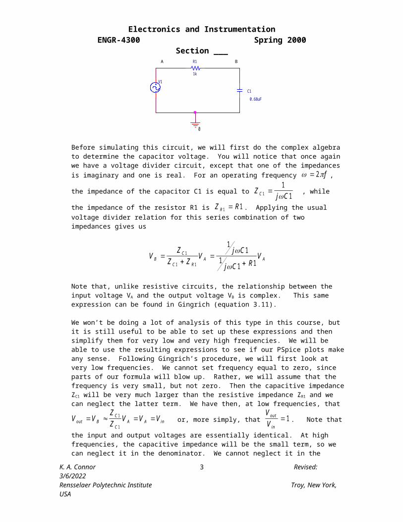
We will return now to the RC circuit we considered back in Experiment 3.
0
V1
R1
1k
C1
0.68uF
A B
Before simulating this circuit, we will first do the complex algebra to determine the capacitor voltage. You will notice that once again we have a voltage divider circuit, except that one of the impedances is imaginary and one is real. For an operating frequency w p 2 f , the impedance of
the capacitor C1 is equal to Zj CC 1
11
w
, while the impedance of the resistor R1 is Z RR 1 1 .
Applying the usual voltage divider relation for this series combination of two impedances gives us
VZ
Z ZV
j C
j C RVB
C
C RA A
1
1 1
11
11 1
w
w
Note that, unlike resistive circuits, the relationship between the input voltage VA and the output voltage VB is complex. This same expression can be found in Gingrich (equation 3.11).
We won’t be doing a lot of analysis of this type in this course, but it is still useful to be able to set up these expressions and then simplify them for very low and very high frequencies. We will be able to use the resulting expressions to see if our PSpice plots make any sense. Following Gingrich’s procedure, we will first look at very low frequencies. We cannot set frequency equal to zero, since parts of our formula will blow up. Rather, we will assume that the frequency is very small, but not zero. Then the capacitive impedance ZC1 will be very much larger than the resistive impedance ZR1 and we can neglect the latter term. We have then, at low frequencies, that
V VZZ
V V Vo u t BC
CA A in 1
1 or, more simply, that
VV
ou t
in1 . Note that the input and output
voltages are essentially identical. At high frequencies, the capacitive impedance will be the small
K. A. Connor Revised: 5/8/2023Rensselaer Polytechnic Institute Troy, New York, USA
2
Electronics and InstrumentationENGR-4300 Spring 2000 Section ___
term, so we can neglect it in the denominator. We cannot neglect it in the numerator, since it is the only term there. Thus, at high frequencies,
V Vj R C
Vj R C
Vout B A in 11 1
11 1w w
or that VV j R C
o ut
in
11 1w . This ratio clearly goes to
zero as
the frequency goes to infinity. It is also negative imaginary and, thus, has a phase of –90o. Aside: While it may seem that terms like low and high, when applied to something like frequency, are fuzzy, ill-defined terms, that is definitely not the case. Here, we mean something quite specific by the expression low frequency. A frequency is only low when the capacitive impedance is so much larger than the resistive impedance that we can neglect the resistive term. We usually need to define the required accuracy to make a statement like this. For example, we can say that a frequency is low as long as the approximate relationship we found between the input and output voltages is within 5% of the full expression. Most of the parts we use in circuits are no more accurate than this, so there is no particular need to do our calculations with better accuracy. In other applications we might need better accuracy.
Simulation – Set up this circuit using PSpice and put a voltage level marker at both points A and B. Do the same AC sweep as before (see below) and then add markers for the real and imaginary voltage. Print out your Probe plots for this case.
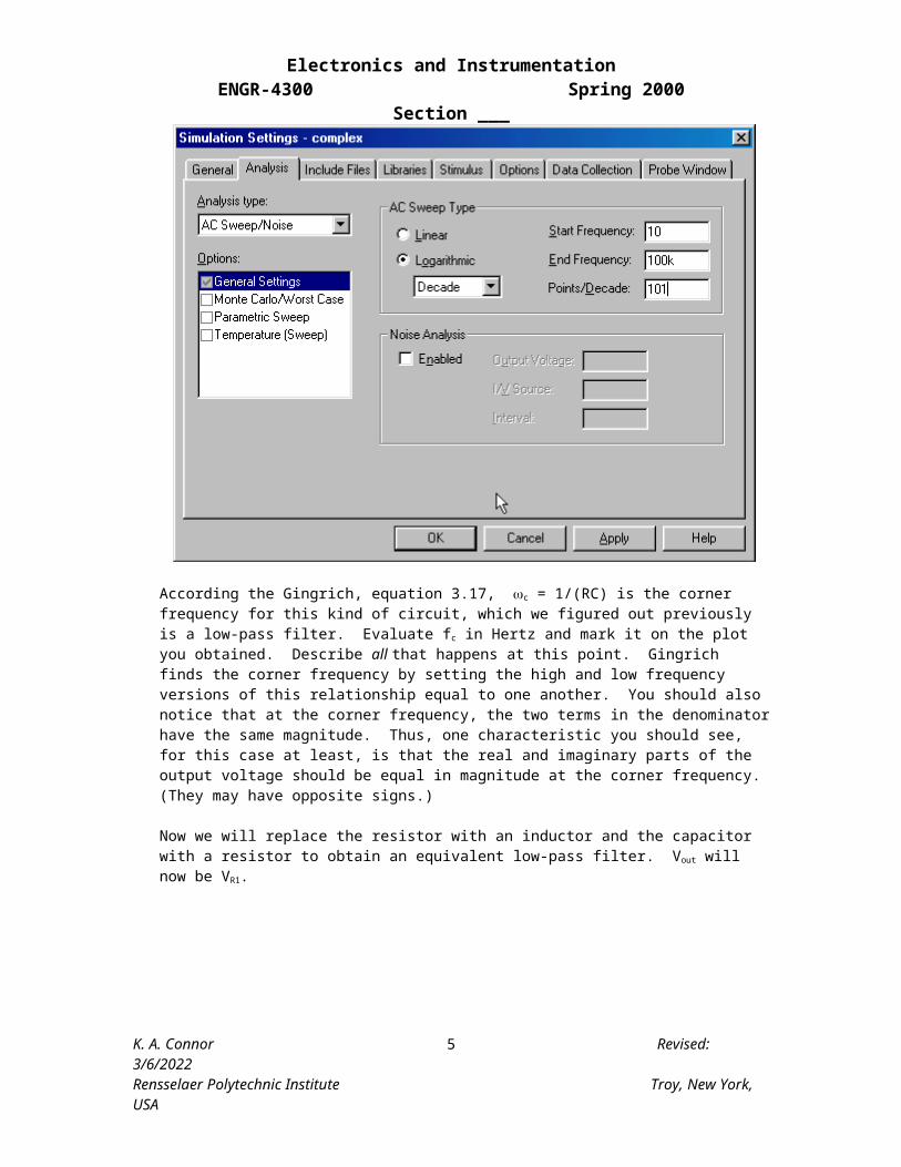
According the Gingrich, equation 3.17, wc = 1/(RC) is the corner frequency for this kind of circuit, which we figured out previously is a low-pass filter. Evaluate fc in Hertz and mark it on the plot you obtained. Describe all that happens at this point. Gingrich finds the corner frequency by setting the high and low frequency versions of this relationship equal to one another. You should also notice that at the corner frequency, the two terms in the denominator have the same magnitude. Thus, one characteristic you should see, for this case at least, is that the real and imaginary parts of the output voltage should be equal in magnitude at the corner frequency. (They may have opposite signs.)
K. A. Connor Revised: 5/8/2023Rensselaer Polytechnic Institute Troy, New York, USA
3

Electronics and InstrumentationENGR-4300 Spring 2000 Section ___
Now we will replace the resistor with an inductor and the capacitor with a resistor to obtain an equivalent low-pass filter. Vout will now be VR1.
0
V1
L1
0.68H
R1
1k
BA
Run the simulation again. You should find that you obtain an identical set of curves. Can you figure out what the general expression is for the corner frequency for this circuit?
Report and Discussion
· Write out the complex expression for Vout in terms of Vin for both of the circuits we have considered. Using this expression, determine the phase shift for very low and very high frequencies.
· What is the expression for the corner frequency of an LR circuit like the one simulated above?
· Both of these circuits turn out to give the same low-pass filter response. Why do you suppose it is that, in practice, we only use the first circuit and not the second?
Background (Continued)
Resonant circuits find wide application in electronics because there are many circumstances in which we wish to produce or block a single frequency. The musical instrument – a Theremin – you saw demonstrated in class is based on four such circuits. There are two common types of resonant circuits, parallel and series combinations of a resistor, an inductor and a capacitor. Figure 3.9 of
K. A. Connor Revised: 5/8/2023Rensselaer Polytechnic Institute Troy, New York, USA
4
Electronics and InstrumentationENGR-4300 Spring 2000 Section ___
Gingrich (seen above) shows series RLC circuits with 4 possible input-output choices. He follows the standard approach to describing such circuits when he addresses their transfer functions
Vout(jw) = H(jw) Vin(jw)
which he first mentions on page 34. Each has a low-frequency and a high frequency approximation, found in the same manner as we have seen for RC and RL circuits. Before considering any of the more complicated algebraic expressions associated with any passive circuit configuration, it is a good idea to determine these limiting cases of H(jw) for frequencies near zero and for very large frequencies. Gingrich chooses to analyze circuit (d), which is a band-reject filter. Note that at both high and low frequencies, the transfer function for this case is equal to one, and thus the input voltage appears unchanged at the output. Also, since the impedance of a capacitor is negative imaginary and that of an inductor is positive imaginary, there will be a frequency wo where the net impedance across the output terminals C and D will be zero. Near this frequency, the output voltage will be zero or at least very small. These frequencies are rejected by this filter which is why it has the name band-reject.
This frequency where the inductive and capacitive impedances cancel is called the resonant frequency. You will recall from Experiment 3, that oscillating systems usually have such a natural resonance. Driving the cantilever beam at its natural resonant frequency caused it to undergo the largest oscillations. You should also recall that there was only a very narrow band of frequencies for which the beam would resonate at all. The measure of width of this band of frequencies is called the Q of the resonator. For a series RLC circuit, Q = woL/R. Thus, larger damping (resistance R) tends to lower the Q.
Question: All oscillators can be assigned a Q value. Do you think that the cantilever beam we have used is high or low Q? How would you go about experimentally determining this? If you have the time, you can do this experiment.
Part B Resonant Circuits
We will now investigate all four of Gingrich’s RLC circuits. We will begin by finding the transfer functions of ideal series RLC circuits under standard limiting conditions so that we will better be able to interpret our results from PSpice simulations and experiments. Then we will use PSpice to simulate a realistic RLC circuit. Finally, we will build such a circuit and see if it performs as expected.
Find the transfer functions for all four RLC circuit configurations shown above at low frequencies, high frequencies and at wo = (LC)-1/ 2. Explain why Gingrich’s name for each configuration is appropriate.
When we build a series RLC circuit, we will use a function generator to produce the input voltage, a resistor, an inductor and a capacitor. However, to either apply the analysis we have just done or to simulate the operation of a circuit using PSpice, we cannot use just a voltage source and three other components, since real devices usually cannot be modeled by a single parameter. Let us go through each of the four parts of this circuit and see what is necessary for realistic analysis or simulation. The circuit we will use is shown below.
Function Generator – We have already seen several times that the function generator has an internal resistance of 50 ohms. Thus, in our realistic circuit, we will use an ideal sinusoidal voltage source V1and a resistor R3 to represent the function generator.
Resistor – Except at very high frequencies, resistors behave in an essentially ideal manner. Thus it is almost always sufficient to represent the resistor in our circuit as R1.
K. A. Connor Revised: 5/8/2023Rensselaer Polytechnic Institute Troy, New York, USA
5

Electronics and InstrumentationENGR-4300 Spring 2000 Section ___
Inductor – Since inductors are made with a long piece of wire, they usually have a significant resistance, in addition to their inductance. Thus, we have included an additional resistor R2 to model the resistance of a real inductor (L1). Typically, accurate representation of realistic inductors requires both of these parameters.
Capacitor – A capacitor typically consists of two large metal plates separated by a thin insulator. If the insulator is very good, almost no current will flow between the plates. Then, like the resistor, the capacitor will behave in an essentially idea manner and we can represent the capacitor in our circuit as C1.
No components we can make are really ideal. Resistors also have inductance and, sometimes, capacitance. Inductors have capacitance. Capacitors have resistance and inductance. Fortunately, we have figured out how to make these devices so that they behave in a nearly ideal manner for quite a broad range of frequencies. However, when we push the limits of some circuit, we have to remember that it may behave as if it consists of more components that we can see when we build it. When the RLC circuit is built, we will only see the three components R1, L1 and C1.
Simulation – Set up the circuit as shown. Assume that the amplitude of V1 is 100mV. Perform an AC sweep from 10 Hz to 100kHz. Since we have now done several AC sweeps, can you explain why we do Decade sweeps rather than Linear sweeps?
0
V1
R1
1k
R2
90
L1
100mH
C1
0.068uF
R3
50
Rather than just plotting the output and input voltages, plot the ratio of Vout to Vin,, which is the transfer function. Then, create a double plot (use the Add Plot Window menu under the Plot menu in Probe). On the top plot display the trace of the absolute value of the transfer function (you can use abs() for this purpose) and on the bottom plot display the trace of the phase of the transfer function (use p() for this purpose). Print out this plot. Label the resonant frequency (you might want to use a cursor for this before you print out the plot). What is the phase shift between the output and input at low and high frequencies?
Experiment – Using values as close as you can find for R, L, and C, build and test the circuit. Before you build it, you should measure the DC resistance of the inductor and the resistor using the multimeter. Also measure the inductance of the inductor and the capacitance of the capacitor using the impedance bridge on the center table. Change your PSpice simulation to correspond to the actual parameters of your circuit. Run the AC sweep again to see what it looks like now. Print out the input and output voltages. Are there any significant differences between the two simulations?
Then test your circuit at 5 representative frequencies that cover the range of your simulation. Be sure that one of your frequencies is low, one is high and one is the resonant frequency of the circuit. There is no magic button for determining either the transfer function or the phase shift between two signals. You will have to do this by displaying the input and output voltages on the ‘scope and manually determining the ratio of the amplitudes and the phase shift. Put the values that you measure on the PSpice plot you made using the actual component values.
Report and Discussion
K. A. Connor Revised: 5/8/2023Rensselaer Polytechnic Institute Troy, New York, USA
6

Electronics and InstrumentationENGR-4300 Spring 2000 Section ___
· What simplification occurs in each of the RLC circuits at the resonant frequency?
· Which of the four RLC circuits produces the largest output voltage for a given input voltage?
· Why is it necessary to plot the phase and the magnitude of the transfer function separately, rather than on the same plot?
· You should have measured a significant resistance for the inductor you used in your hardware implementation. How could such an inductor be made with lower resistance?
Note: The discussion of AC Circuits in the Engineer on a Disk link found in the Helpful Info section of the course webpage is useful to look over for this experiment.http://claymore.engineer.gvsu.edu/~jackh/eod/electric/circanal/circanal.html
K. A. Connor Revised: 5/8/2023Rensselaer Polytechnic Institute Troy, New York, USA
7
Electronics and InstrumentationENGR-4300 Spring 2000 Section ___
Experiment 5Please list the names of all group members. A TA or instructor will initial a participation box each class day you attend and participate in this experiment. When you have completed all of the experimental and simulation activities, have a TA or instructor initial under completed. They should also look over what you have done to be sure that your results are useful. If you are unable to attend class for any reason, you can make up the work during an open shop time. The maximum participation grade is 5 points.
Student Name Participation Participation Participation Completed
Date Pts
Please answer any questions asked above under the Report and Conclusions sections. Also, attach any plots requested. On each plot, describe what is being displayed and why the results make sense. Include a hand-drawn or computer drawn circuit diagram for any PSpice output or plots of measurements indicating where and how the measurements were made. Summarize the key points of this experiment. Discuss any problems you encountered or mistakes you made and how you addressed them.
Names:
1. ____________________________
2. ____________________________
3. ____________________________
4. ____________________________
Grade: ___________ (Out of 25)
K. A. Connor Revised: 5/8/2023Rensselaer Polytechnic Institute Troy, New York, USA
8