Excalibur EPXA10 DDR Development Board Hardware Reference...
78
MNL-EXCDDRDEVBRD-1.3 EPXA10 101 Innovation Drive San Jose, CA 95134 (408) 544-7000 http://www.altera.com Hardware Reference Manual April 2003 Version 1.3 DDR Development Board
Transcript of Excalibur EPXA10 DDR Development Board Hardware Reference...

MNL-EXCDDRDEVBRD-13
EPXA10
101 Innovation DriveSan Jose CA 95134(408) 544-7000httpwwwalteracom
Hardware Reference ManualApril 2003
Version 13
DDR Development Board
ii Altera Corporation
Excalibur EPXA10 DDR Development Board Hardware Reference Manual
Copyright 2003 Altera Corporation Altera The Programmable Solutions Company the stylized Altera logo specific device designations and allother words and logos that are identified as trademarks andor service marks are unless noted otherwise the trademarks and service marks of AlteraCorporation in the US and other countries All other product or service names are the property of their respective holders Alteraproducts are protected under numerous US and foreign patents and pending applications mask work rights and copyrightsAltera warrants performance of its semiconductor products to current specifications in accordance with Alterarsquos standard warrantybut reserves the right to make changes to any products and services at any time without notice Altera assumes no responsibility orliability arising out of the application or use of any information product or service described herein except as expressly agreed toin writing by Altera Corporation Altera customers are advised to obtain the latest version of device specifications before relying onany published information and before placing orders for products or services All rights reserved
About this Manual
This manual provides comprehensive information about the Alterareg EPXA10 DDR development board
Table 1 shows the manual revision history
How to Find Information
The Adobe Acrobat Find feature allows you to search the contents of a PDF file Click on the binoculars icon in the top toolbar to open the Find dialog box
Bookmarks serve as an additional table of contents Thumbnail icons which provide miniature previews of each page
provide a link to the pages Numerous links shown in green text allow you to jump to related
information
Table 1 Revision History
Date Description
April 2003 Improved expansion header tables
January 2003 Amended EPC16 configuration device section
December 2002 Changed board device number
November 2002 First publication
Altera Corporation iii
About this Manual EPXA10 DDR Development Board Hardware Reference Manual
How to Contact Altera
For the most up-to-date information about Altera products go to the Altera world-wide web site at httpwwwalteracom
For additional information about Altera products consult the sources shown in Table 2
Note(1) You can also contact your local Altera sales office or sales representative
Table 2 How to Contact Altera
Information Type Access USA amp Canada All Other Locations
Altera Literature Services
Electronic mail lit_reqalteracom (1) lit_reqalteracom (1)
Non-technical customer service
Telephone hotline (800) SOS-EPLD (408) 544-7000 (730 am to 530 pm Pacific Time)
Fax (408) 544-7606 (408) 544-7606
Technical support Telephone hotline (800) 800-EPLD(700 am to 500 pm Pacific Time)
(408) 544-7000 (1)(730 am to 530 pm Pacific Time)
Fax (408) 544-6401 (408) 544-6401 (1)
World-wide web site httpwwwalteracommysupport httpwwwalteracommysupport
FTP site ftpalteracom ftpalteracom
General product information
Telephone (408) 544-7104 (408) 544-7104 (1)
World-wide web site httpwwwalteracom httpwwwalteracom
iv Altera Corporation
EPXA10 DDR Development Board Hardware Reference Manual About this Manual
Typographic Conventions
The Excalibur EPXA10 DDR Development Board Hardware Reference Manual uses the typographic conventions shown in Table 3
Table 3 Conventions
Visual Cue Meaning
Bold Type with Initial Capital Letters
Command names dialog box titles checkbox options and dialog box options are shown in bold initial capital letters Example Save As dialog box
bold type External timing parameters directory names project names disk drive names filenames filename extensions and software utility names are shown in bold type Examples fMAX QuartusII directory d drive chiptripgdf file
Bold italic type Book titles are shown in bold italic type with initial capital letters Example 1999 Device Data Book
Italic Type with Initial Capital Letters
Document titles are shown in italic type with initial capital letters Example AN 75 (High-Speed Board Design)
Italic type Internal timing parameters and variables are shown in italic type Examples tPIA n + 1Variable names are enclosed in angle brackets (lt gt) and shown in italic type Example ltfile namegt ltproject namegtpof file
Initial Capital Letters Keyboard keys and menu names are shown with initial capital letters Examples Delete key the Options menu
ldquoSubheading Titlerdquo References to sections within a document and titles of Quartus II Help topics are shown in quotation marks Example ldquoConfiguring a FLEX 10K or FLEX 8000 Device with the BitBlastertrade Download Cablerdquo
Courier type Signal and port names are shown in lowercase Courier type Examples data1 tdi input Active-low signals are denoted by suffix _n eg reset_n
Anything that must be typed exactly as it appears is shown in Courier type For example cquartusIIqdesignstutorialchiptripgdf Also sections of an actual file such as a Report File references to parts of files (eg the AHDL keyword SUBDESIGN) as well as logic function names (eg TRI) are shown in Courier
1 2 3 and a b c Numbered steps are used in a list of items when the sequence of the items is important such as the steps listed in a procedure
Bullets are used in a list of items when the sequence of the items is not important
v The checkmark indicates a procedure that consists of one step only
1 The hand points to information that requires special attention
r The angled arrow indicates you should press the Enter key
f The feet direct you to more information on a particular topic
Altera Corporation v
Notes
Contents
How to Find Information iiiHow to Contact Altera ivTypographic Conventions vFeatures 9Functional Overview 10Board Components 10Interfaces 14
PCI Interface 1410100 Ethernet Parallel Interface 16Serial IO Interfaces 18Memory Interfaces 19LED amp Switch Interfaces 22Trace Port Interface 2610-Pin IDC Header Interface 26Expansion Header Interface 27
Jumper Configuration 32Clocks 35
CLK_REF amp the FPGA Clocks 37MAX 3032 38Embedded Stripe Clocks 38Jumper Configuration for the Clock Input 40Sources for the EPXA10 Clocks 40
Device Configuration 41Booting from Flash Memory 41Configuring Using the EPC16 42Configuring Using JTAG 43Configuration Schemes 44
Debugging Features 44Third-Party Debugging Tools 45JTAG Interfaces 45Power Supply 47
Test Points 51Signals 52
UART 52PCI 53Trace Port 54ConfigurationDebugging Interfaces 55
Pin-Outs 57Configuration 57
Altera Corporation vii
Contents EPXA10 DDR Development Board Hardware Reference Manual
DDR SDRAM Interface 59EBI 61PCI 63UART1 amp UART2 64Ethernet 64Fast IO Pins 65User LEDs Switches amp Push Button Switches 65Trace Port 66IDC 10-Pin Header 66Expansion Header 67
General Usage Guidelines 74Anti-Static Handling 74Power-Up 74Power Consumption 74PCI Cards 74Unused EPXA10 Device Pins 75Test Core Functionality 75
viii Altera Corporation
Specifications
1
EPXA10 DDR DevelopmentBoard
Features Powerful development board for embedded processor FPGA designsndash Features an EPXA10F1020C1 devicendash Supports intellectual property-based (IP-based) designs using a
microprocessor Industry-standard interconnections
ndash 10100 megabits per second (Mbps) Ethernet with full and half duplexing
ndash Two 32-bit peripheral component interconnect (PCI) connectors
1 These features require additional IP blocks contact Altera for further details
ndash Two RS-232 ports Memory subsystem
ndash 32-Mbyte flash memoryndash 128-Mbyte DDR SDRAM
Multiple clocks for communications system design Multiple ports for configuration and debugging
ndash IEEE Std 11491 Joint Test Action Group (JTAG)ndash Support for configuring the EPXA10 device using flash memory
an EPC16 or a MasterBlastertrade or ByteBlasterMVtrade cable Expansion headers for greater flexibility and capacity
ndash Four expansion headers for daughter-card accessndash 33-V5-V12-Vndash12-V expansionprototype headers to
support up to 502 user IO pins Two PCI connectors accommodate 33-V and universal PCI
expansion cards Additional user-interface features
ndash One user-definable 9-bit dual in-line package (DIP) switch blockndash Four user-definable push-button switchesndash Eight user-definable LEDsndash One IDC plugmdash10 pins 254 mm pitch with 8 user-definable
connection and two power and ground pins Test points provided to facilitate system development Trace port connections
Altera Corporation 9
EPXA10 DDR Development Board Hardware Reference Manual
Functional Overview
Designers can use the EPXA10 DDR development board as a desktop development system It provides a hardware platform to start developing embedded systems immediately and delivers clocks debugging and trace facilities to support the system under development in an Excaliburtrade EPXA10 device
The EPXA10 DDR development board provides a flexible powerful debug and development environment Designers can use the board for a variety of purposes including building and emulating systems for special requirements and conducting trace and debug investigations
Board Components
This section introduces a brief overview of the components of the EPXA10 DDR development board which is shown in Figure 1 on page 11
10 Altera Corporation
EPXA10 DDR Development Board Hardware Reference Manual
Figure 1 EPXA10 DDR Development Board Layout
290 mm
290
mm
Power supply For greater detail see Figure 15 on page 48
Clocks For greater detail see Figure 11 on page 37
Altera Corporation 11
EPXA10 DDR Development Board Hardware Reference Manual
The EPXA10 DDR development board features the largest member of the Excalibur family the EPXA10 The EPXA10 features an integrated microprocessor system with the APEX 20KE architecture in a 1020-pin FineLine BGAtrade package
Table 1 lists the main features of the device
In addition the EPXA10 provides a variety of peripherals as listed in Table 2
Table 1 EPXA10 Device Features
Feature Capacity
Maximum system gates 1772000
Typical gates 1000000
LEs 38400
ESBs 160
Maximum RAM bits 327680
Maximum macrocells 2560
Maximum user IO pins 521
Table 2 EPXA10 Device Peripherals
Peripheral Description
ARM922T 32-bit RISC processor For speed grade ndash1 up to 200 MHzFor speed grade ndash2 up to 166 MHzFor speed grade ndash3 up to 133 MHz
ETM9 trace module Used for software debugging
Interrupt controller Used for the interrupt system
Internal single-port SRAM 256 Kbytes
Internal dual-port SRAM 128 Kbytes
SDRAM controller Interfaces between the internal system bus and SDRAM
External DDR SDRAM Refer to the Excalibur Devices Hardware Reference Manual for details of supported sizes
Expansion bus interface (EBI) Interfaces to flash memory
External flash memory Refer to the Excalibur Devices Hardware Reference Manual for details of supported sizes
Watchdog timer Protects the system against software failure
UART Facilitates serial communication
Reset controller Resets the device
12 Altera Corporation
EPXA10 DDR Development Board Hardware Reference Manual
f Refer to the Excalibur Devices Hardware Reference Manual for details about EPXA10 devices
Figure 2 illustrates the relationship between the EPXA10 device and the development board peripherals
Figure 2 EPXA10 DDR development Board Block Diagram
ExcaliburEPXA10
ExternalConnectors
Configuration
PCIConnectors
EthernetConnector
UARTConnectors
FlashMemory
DDRSDRAM
Altera Corporation 13
EPXA10 DDR Development Board Hardware Reference Manual
Interfaces Table 3 lists the interfaces on the EPXA10 DDR development board
PCI Interface
Two PCI slots U9 and U10 are implemented on the EPXA10 DDR development board The 32-bit interface runs at up to 33 MHz and operates at 33 V only it complies with PCI Local Bus Specification Revision 22 The slots must be used solely with 33 V and universal PCI cards
1 Do not force a 5-V PCI card into a 33-V PCI connector this could damage the EPXA10 device
User IO pins are provided for the PCI interfaces Table 52 on page 63 lists the PCI signal pin assignments
Table 3 Development Board Interfaces
Interface Description
PCI connectors The connectors operate at 32-bit 33 MHz and can be used by designers to connect standard commercially-available 33-V (only) and universal PCI cards
10100 Ethernet with full- and half-duplexing
This interface consists of a connector transceiver and transformer The MAC is implemented in the Altera device as an IP block The connection between the MAC and the transceiver is a standard MII
IEEE Std 488 RS-232 serial interfaces
This interface is a 120-V transceiver with 235-kbps data rate in a TSSOP package
Debuggingprogramming ports
The board supports in-circuit debugging by means of the MasterBlaster ByteBlasterMV or Multi-ICE cables
MICTOR connector This connector provides debugging facilities for the trace port
10-pin IDC connector Facilitates access to the user IO
Expansion headers These connectors allow designers to stack multiple daughter boards as required
User IO pins The expansion header provides up to 502 user IO pins that connect directly to the EPXA10 device supporting custom interfaces (see Table 59 on page 67)
14 Altera Corporation
EPXA10 DDR Development Board Hardware Reference Manual
EPXA10 Device Signal Definitions for PCI Cards
Table 4 lists the PCI signals for which EPXA10 device signals are required to implement the PCI interface See Table 52 on page 63 for pin-out details
Some signals are not included in Table 4 IDSEL is a PCI signal used as a device select for configuration cycles and is generally connected to one of the address lines Table 5 lists the IDSEL signal connections
Table 4 EPXA10 Device Signal Definitions for PCI Cards
Function PCI Signal Number
Address and data AD[310]
CBE[30]
PAR
37
Interface control FRAME
TRDY
IRDY
STOP
DEVSEL
LOCK
6
Error reporting PERR
SERR
2
Arbitration PRSNT1
PRSNT2
REQ1
REQ2
GNT1
GNT2
6
Interrupts INTA
INTB
INTC
INTD
4
System CLK2
PCI_RST
2
Table 5 IDSEL Signal Connections
Board Reference PCI Slot EPXA10 Board Reference
U10A26 1 AJ19
U9A26 2 AK19
Altera Corporation 15
EPXA10 DDR Development Board Hardware Reference Manual
Board-Level Issues
The PCI interface requires no devices on the board level if the PCI is implemented as an IP core in the EPXA10 device All of the power supplies are provided when the ATX power supply is connected on the EPXA10 DDR development board
Table 6 lists the PCI interface characteristics
10100 Ethernet Parallel Interface
The Ethernet interface consists of a transceiver or PHY layer and associated discrete components You can use the interface to implement an Ethernet media access controller (MAC) in the EPXA10 device As shown in Table 43 on page 53 the interface consists of standard media-independent interface (MII) and additional signals Table 7 details the devices used to implement the Ethernet interface
Table 6 PCI Interface Characteristics
Interface Features IO Pins Voltages Clock Speed
PCI Interface 55 plus clock +33 V +5 V plusmn12 V 33 MHz
Table 7 Ethernet Interface Device Reference
Board Reference
Part Number Manufacturer Website Address Description
U8 78Q2120-64CGT (TQFP64) TDK wwwtdkcom Fast Ethernet MII transceiver
U4 PE-68515L Pulse wwwpulseengcom 10100-BASE T single-port transformer module
P3 AMP 555078-1 AMP wwwampcom 8-pin PCB RJ45 data socket
16 Altera Corporation
EPXA10 DDR Development Board Hardware Reference Manual
Ethernet LEDs
Table 8 lists the LEDs used for the Ethernet on the EPXA10 DDR development board
Ethernet Switches
Table 9 lists the switches used for the Ethernet device in the DIPSW2 dip-switch bank and Table 10 on page 18 lists the TECH switches which are used to set the Ethernet decoding protocol
Table 8 Ethernet LEDs
Board Reference
Description
LEL Link LED This is set on during linkup
LEDTX Transmit LED This is set on during transmission
LEDRX Receive LED This is set on during receipt
LEDFDX Full-duplex LED This set on for full-duplex mode and off for half-duplex
LEDCOL Collision LED This is set on in half-duplex mode when a collision occurs and is held off in full-duplex mode
LEDBTX 100-BASE TX LED This is set on for 100-BASE T connection but off otherwise
LEDBT 10-BASE T LED This is set on for 10-BASE T connection but is off otherwise
Table 9 DIPSW2 Switch Connections
Board Reference Identifier Function
DIPSW2_1 ANEGA Auto-negotiation enable
DIPSW2_2 TECH0
Used to specify the Ethernet decodingDIPSW2_3 TECH1
DIPSW2_4 TECH2
DIPSW2_5 PHYAD0
Physical Address
DIPSW2_6 PHYAD1
DIPSW2_7 PHYAD2
DIPSW2_8 PHYAD3
DIPSW2_9 PHYAD4
Altera Corporation 17
EPXA10 DDR Development Board Hardware Reference Manual
Serial IO Interfaces
There can be two UARTs in the EPXA10 device A dedicated UART is located in the embedded stripe optionally an IP UART can be implemented in the FPGA connected to 33-V standard EPXA10 IO pins Each UART is connected to a transceiver (U2 for the embedded stripe UART and U3 for the IP UART) to convert LVTTL voltage for RS-232 compatibility at up to 256 Kbps Each UART also has its own DB9 male RS-232 connector wired as a DTE
1 The transceiver uses a 33-V power supply If the RS-232 input pins are used as general-purpose outputs contention occurs because the bus transceiver is always active If these pins are not used as part of a design ensure that they remain in the high-impedance state All unused IO pins can be set to tri-state mode in the Quartus II software (see ldquoUnused EPXA10 Device Pinsrdquo on page 75)
Table 11 provides information on the devices used to implement the RS-232 interface
See Table 42 on page 52 for information on the RS-232 signals
Table 10 Ethernet Protocol Decoding
TECH [20] Function0 0 0 No technology capability
1 1 1 Both 10-BASE T and 100-BASE T
0 0 1 10-BASE T half duplex
0 1 0 100-BASE T half duplex
0 1 1 Both 10-BASE T and 100-BASE T half duplex
1 0 0 None
1 0 1 10-BASE T fullhalf duplex
1 1 0 100-BASE T fullhalf duplex
Table 11 RS-232 Interface Device Reference
Board Reference
Part Number Manufacturer Website Address Description
U2 MAX3241 Maxim wwwmaxim-iccom RS-232 DTE transceiver (connects to the UART in the stripe using connector P1)
U3 MAX3241 Maxim wwwmaxim-iccom RS-232 DTE transceiver (connects to the soft UART in the FPGA using connector P2)
18 Altera Corporation
EPXA10 DDR Development Board Hardware Reference Manual
Table 12 gives the UART interface characteristics
Table 8 lists the UART LEDs on the EPXA10 DDR development board
Memory Interfaces
The EPXA10 DDR development board supports the following types and capacities of on-board memory as listed in Table 14
DDR SDRAM
Four 256-Mbit DDR SDRAM chips are connected to the SDRAM controller giving a total of 128 Mbytes of 32-bit memory Figure 3 on page 20 shows how they are arranged
Table 12 DTE UART Interface Characteristics
Features IO Pins Voltage (V)
UART 1 TX RX amp control 7 33
UART 2 TX RX amp control 7 33
Table 13 UART LEDs
Board Reference Signal Description
TX_UART1 UART1_TXD This LED indicates activity on the line
RX_UART1 UART1_RXD This LED indicates activity on the line
TX_UART2 UART2_TXD This LED to indicates activity on the line
RX_UART2 UART2_RXD This LED indicates activity on the line
Table 14 Development Board Memory Characteristics
Type Address Lines
Data Lines
Control Lines
Memory Organization Size
DDR SDRAM 15 32 3 4 M times 32 times 4 banks 128 Mbytes 32-bit
Flash 25 16 6 4 times 8 Mbytes 32 Mbytes
Altera Corporation 19
EPXA10 DDR Development Board Hardware Reference Manual
Figure 3 DDR SDRAM Interface
Table 15 provides information on the devices used to implement the DDR SDRAM interfaces
SD_CS0
SD_DQS0[30]
SD_DQM0[30]
SD_DQ[310]
SD_A[120]
SD_A[1413]
x1 x2 x3
y3y2y1
BA[10] BA[10] BA[10] BA[10]
SD_DQ[70] SD_DQ[158] SD_DQ[2316] SD_DQ[3124]
x1 SD_DQS1[30]x2 SD_DQS2[30]x3 SD_DQS3[30]
y1 SD_DQM1[30]y2 SD_DQM2[30]y3 SD_DQM3[30]
Key
Bank 0 Bank 1 Bank 2 Bank 3
Exc
alib
ur E
PX
A10
IO[70] IO[158] IO[2316] IO[3124]
Table 15 DDR SDRAM Interface Device Reference
Board Reference
Part Number Manufacturer Website Address Description
DDR1 MT46V32M8 Micron wwwmicroncom 256 Mbit times 8-bit SDRAM
DDR2 MT46V32M8 Micron wwwmicroncom 256 Mbit times 8-bit SDRAM
DDR3 MT46V32M8 Micron wwwmicroncom 256 Mbit times 8-bit SDRAM
DDR4 MT46V32M8 Micron wwwmicroncom 256 Mbit times 8-bit SDRAM
20 Altera Corporation
EPXA10 DDR Development Board Hardware Reference Manual
Table 16 shows the timing parameters that should be used when setting up the EPXA10 SDRAM controller for use with Micron MT46V16M8 DDR devices
Flash Memory
Four 8-Mbyte flash memory chips are connected to the EBI of the EPXA10 device giving a total of 32-Mbytes of 16-bit memory (see Figure 4)
Figure 4 Flash Memory Interface
Table 16 Micron MT46V16M8 DDR Timing Parameters
Parameter Value
Active to Read or Write (RCD) 20ns
Active to Precharge command (RAS) 45ns
Active bank A to Active bank B command (RRD) 15ns
Precharge command period (RP) 20ns
Write recovery time (WR) 15ns
Active to Active command period (RC) 65ns
Auto Refresh period (RFC) 65ns
Auto Refresh command interval (RFSH) 15625ns
CAS latency (CL) 2 ndash 25
Burst Length (BL) 8
Row address bits 12
Column address bits 10
Bank address bits 2
EPXA10
EBI
A1-A21
D0-D15
OE WE CE
A0-A20
Flash Memory (4 x 8 Mbyte)
33 V 12 V
Programmingvoltage
1 2 3 4
Altera Corporation 21
EPXA10 DDR Development Board Hardware Reference Manual
Table 17 provides information on the devices used to implement the flash memory interfaces
LED amp Switch Interfaces
The EPXA10 DDR development board provides a variety of LED and switch interfaces Some are user-definable and some are function-specific Figure 5 on page 23 shows the location of LEDs and switches on the development board
Table 17 Flash Memory Interface Device Reference
Reference Part Number Manufacturer Website Address Description
FLASH1 28F640C3 Intel wwwIntelcom 256 Mbit times 16-bit flash memory
FLASH2 28F640C3 Intel wwwIntelcom 256 Mbit times 16-bit flash memory
FLASH3 28F640C3 Intel wwwIntelcom 256 Mbit times 16-bit flash memory
FLASH4 28F640C3 Intel wwwIntelcom 256 Mbit times 16-bit flash memory
22 Altera Corporation
EPXA10 DDR Development Board Hardware Reference Manual
Figure 5 Switches amp LEDs on the EPXA10 DDR development Board
User-defined push-button switches See Table 22 on page 26 for details
Push-button switches See Table 21 on page 26 for details
User-defined LEDs See Table 20 on page 25 for details
Application LEDs See Table 19 on page 24 for details
Ethernet switches See Table 9 on page 17 for details
Ethernet LEDs See Table 19 on page 24 for details
Application LEDs See Table 19 on page 24 for details
User-defined switches See Table 18 on page 24 for details
Altera Corporation 23
EPXA10 DDR Development Board Hardware Reference Manual
User-Defined LEDs
On the EPXA10 DDR development board there are eight user-definable LEDs They connect directly to the EPXA10 device IO pins and can be used for any kind of application
Table 18 lists the user LEDs on the development board
Table 56 on page 65 provides more information on EPXA10 device pins connected to LEDs
Function-Specific LEDs
LEDs are also used for specific application functions such as the configuration RS-232 and Ethernet interfaces Table 19 lists the function-specific LEDs their power supply voltage their connection details and their use
Table 18 LED Interface Characteristics
Feature Board Reference EPXA10 IO Pin Voltage (V)
USER_LED7 U26 T6 33
USER_LED6 U25 U7 33
USER_LED5 U24 V8 33
USER_LED4 U23 V7 33
USER_LED3 U22 U6 33
USER_LED2 U21 V5 33
USER_LED1 U20 U5 33
USER_LED0 U19 V6 33
Table 19 Function-Specific LED Usage (Part 1 of 2)
Signal Board Reference
EPXA10 IO Pin (or Board Connector)
Description Voltage (V)
VCC_ndash5V U27 ndash5-V power supply indicator ndash5
VCC_5V U28 5-V power supply indicator 5
VCC_25V U29 25-V power supply indicator 25
VCC_12V U30 12-V power supply indicator ndash12
VCC_33V U31 33-V power supply indicator 33
VCC_ndash12V U32 ndash12-V power supply indicator ndash12
VCC_18V U33 18-V power supply indicator 18
LEDL LEDL (1) LED link signal indicator 33
24 Altera Corporation
EPXA10 DDR Development Board Hardware Reference Manual
Note(1) These pins are connected to the Ethernet transceiver and not directly to the EPXA10 device
Switch Interfaces
In addition to the dip-switches used for the Ethernet interface which are listed in Table 9 on page 17 the EPXA10 DDR development board provides nine user-definable switches in another dip-switch block four push-button switches two dedicated reset switches and a switch to generate an interrupt on the EBI controller Table 20 documents the interface characteristics of the dip-switch block DIP_SW1
LEDTX LEDTX (1) LED transmit signal indicator 33
LEDRX LEDRX (1) LED receive signal indicator 33
LEDFDX LEDFDX (1) LED full-duplex signal indicator 33
LEDCOL LEDCOL (1) LED collision signal indicator 33
LEDBTX LEDBTX (1) LED 100-BASE TX signal indicator 33
LEDBT LEDBT (1) LED 10-BASE T signal indicator 33
UART1_TXD TX_UART1 D28 Embedded stripe UART signal indicator 33
UART1_RXD RX_UART1 D29 Embedded stripe UART signal indicator 33
UART2_TXD TX_UART2 J29 FPGA UART signal indicator 33
UART2_RXD RX_UART2 K29 FPGA UART signal indicator 33
INIT_DONE INIT_DONE D14 Used by FPGA initialization signifies that initialization is complete
33
Table 19 Function-Specific LED Usage (Part 2 of 2)
Signal Board Reference
EPXA10 IO Pin (or Board Connector)
Description Voltage (V)
Table 20 DIPSW1 Switch Connection
Board Reference EPXA1 IO Pin Board Connector Voltage (V)
DIPSW11 U8 U1812 33
DIPSW12 T5 U1813 33
DIPSW13 V4 U1815 33
DIPSW14 V10 U1816 33
DIPSW15 T7 U1817 33
DIPSW16 W12 U1819 33
DIPSW17 U9 U1820 33
DIPSW18 V11 U1821 33
DIPSW19 R6 U1823 33
Altera Corporation 25
EPXA10 DDR Development Board Hardware Reference Manual
The push-button switches and integrated LEDs are connected to the EPXA10 IO pins Tables 21 and 22 detail the push-button switches
Trace Port Interface
A matched-impedance connector (MICTOR) is connected to the ETM9 trace module It is used in conjunction with trace tools such as ARM Trace and Lauterbach to debug the software in real time ETM9 trace tools are connected to PROC_JTAG signals Table 23 gives details of the device used
10-Pin IDC Header Interface
The 10-pin header interface HEADER1 facilitates connection to pins on the expansion header which in turn connect to the user IO on the EPXA10 device The pins on the header are arranged in a 5 times 2 matrix
Table 21 Push-Button Switches
Board Reference EPXA10 IO Pin
Signal Use Voltage (V)
SW_RESET R30 NCONFIG Generates a warm reset 33
SW_DEV_CLR_N H3 GLOBNRS Resets the FPGA 33
SW4 INT G25 int_extpin_n Generates an interrupt on the EBI interface when enabled by the interrupt controller also connected to user-defined IO
33
Table 22 User-Definable Push-Button Switches
Board Reference EPXA10 IO Pins
Board Connector
Signal Voltage (V)
SW1 T8 U1824 USER_PB0 33
SW2 R5 U1825 USER_PB1 33
SW3 U4 U1827 USER_PB2 33
SW4 U10 U1828 USER_PB3
also
int_extpin_n
33
SW4 INT G25 33
Table 23 Interface Device Reference
Board Reference
Part Number Manufacturer WebsiteAddress
Description
TRACE PORT AMP ref 2-767004-2 AMP httpwwwampcom Connected to the ETM9
26 Altera Corporation
EPXA10 DDR Development Board Hardware Reference Manual
Expansion Header Interface
The EPXA10 DDR development board hosts the EPXA10 device and four expansion headers which are implemented on the board for use with daughter cards The expansion headers are implemented using Samtec TOLC 200-pin connectors as listed in Table 24 on page 27 They are connected to IO pins on the EPXA10 device Headers U16 U17 and U18 include +5-V +33-V plusmn12-V and ground signals as well as IO signals Header U15 only has IO signals and clock signals
Table 24 on page 27 provides information on the devices used to implement the expansion header interface
Note(1) Altera recommends that you use Samtec SOLC-150-02-F-Q for the daughter board connectors
Table 25 lists the expansion header interface characteristics
All USER LEDs switches push buttons and the 10-pin IDC connector are accessible from the expansion headers
The expansion headers can be used to interface to special-function daughter cards contact your Altera representative for details of the daughter cards available By using the IO pins on the EPXA10 device and power supplies from the EPXA10 DDR development board you can design expansion cards to your specific requirements
Table 24 Expansion Header Interface Device Reference
Board Reference
Part Number Manufacturer Website Address Description
U15 SAMTECTOLC-150-32-F-Q
Samtec wwwsamteccom Connector to expansion card
U16 SAMTECTOLC-150-32-F-Q
Samtec wwwsamteccom Connector to expansion card
U17 SAMTECTOLC-150-32-F-Q
Samtec wwwsamteccom Connector to expansion card
U18 SAMTECTOLC-150-32-F-Q
Samtec wwwsamteccom Connector to expansion card
Table 25 Expansion Header Interface Characteristics
Interface IO Pins Signalling Voltage (V)
Clock Voltages (V)
Expansion header 501 plusmn33 33 MHz +33 +5 plusmn12
Altera Corporation 27
EPXA10 DDR Development Board Hardware Reference Manual
The connectors are stackable so more than one card can be plugged on each header allowing you to develop different cards for individual modules within a complex design
1 Refer to Figures 6 to 9 for mechanical drawings of the board expansion headers and Tables 56 through 59 for EPXA10 pin details and their connections on the expansion headers
Figure 6 on page 28 shows the location of the expansion headers on the EPXA10 DDR development board
Figure 6 EPXA10 DDR development Board TOLC Expansion Header Connections
U15
U16
U17
EPXA10
U18
28 Altera Corporation
EPXA10 DDR Development Board Hardware Reference Manual
The dimensions given in Figures 7 to 9 are inches measured from the centre of the pad
Figure 7 gives dimensions for the TOLC expansion headers categorized in Table 24 on page 27
Figure 7 EPXA10 DDR development Board TOLC Dimensions
1 All dimensions are in inches
To connect to the motherboard a daughter board must use SOLC connectors for which dimensions are given in Figure 8 on page 30
38000
195
00
272
50
08700
06830
Altera Corporation 29
EPXA10 DDR Development Board Hardware Reference Manual
Figure 8 Daughter Board SOLC Dimensions
a
1 All dimensions are in inches
Figure 9 on page 31 is a mechanical diagram giving the position of the TOLC connectors on the motherboard layout
1 The PCB footprints for TOLC and SOLC connectors differ
38000
19400
272
50
06690
08570
30 Altera Corporation
EPXA10 DDR Development Board Hardware Reference Manual
Figure 9 Mechanical Diagram of the EPXA10 DDR development Board Expansion Headers
1 All dimensions are in inches
210
0
0900
1400
1600
DIA 0132 x 4 off
XA1 center
0 0
Centre ofU15 pin 1PCB pad
0125
1725
2250 2600 2800
1250
1370
2050
2200
2075
2300
2800
0
X
X
X
X
X
X
X
X
OO
OO
Centre ofU16 pin 1PCB pad
Centre ofU18 pin 1PCB pad
Centre ofU17 pin 1PCB pad
Altera Corporation 31
EPXA10 DDR Development Board Hardware Reference Manual
To design a matching daughter board designers must do one of the following
Base designs on the SOLC expansion header dimensions given in Figure 8 on page 30
Translate dimensions from the TOLC motherboard dimensions
Jumper Configuration
The jumpers on the EPXA10 DDR development board serve several functions
Clock distribution Enabling clocks Selecting clocks JTAG configuration Enabling the PLL interface Selecting VPP voltage Driving logic signals to the MAX 3032 device
Figure 10 on page 33 shows the location of the jumpers on the development board
32 Altera Corporation
EPXA10 DDR Development Board Hardware Reference Manual
Figure 10 Jumper Locations
JP_AGND2GND
JP8
JP3
JP2
JP1
JP6
JP5
JP4
MSEL0
MSEL1
JSELECT
BOOT_FLASH
DEBUG_EN
JP7
JP_VPP
JF1JF2
JP9JP10
Altera Corporation 33
EPXA10 DDR Development Board Hardware Reference Manual
Table 26 lists the jumpers on the EPXA10 DDR development board
Note(1) Used to select configuration mode See ldquoConfiguration Schemesrdquo on page 44(2) Connects clock 3 for LVDS See AN 115 Using the ClockLock and ClockBoost PLL Features in APEX Devices(3) Determines whether serial or dual JTAG chains are used for debugging(4) Enablesdisables debugging(5) Connects clocks 1 or 2 to the Ethernet clock(6) Enablesdisables the Ethernet clock(7) Enablesdisables clocks(8) JF1 and JF2 used in combination to drive a signal to specific pins on the MAX 3032 device
Table 26 Jumpers on the EPXA10 DDR development Board
Jumper amp Description
EPXA10 IO Pin (Board Connection)
Pins 1-2 Connected Pins 2-3 Connected Default
JP1 (7) X1 Osc Disabled X1 Osc Enabled 2-3
JP2 (7) X2 Osc Disabled X2 Osc Enabled 2-3
JP3 (5) CLK1=Ext_Osc0 CLK1=TX_CLK 1-2
JP4 (7) X4 Osc Disabled X4 Osc Enabled 2-3
JP5 (7) X5 Osc Disabled X5 Osc Enabled 2-3
JP6 (7) X6 Osc Disabled X6 Osc Enabled 2-3
JP7 (6) PHY 25MHz Clock Disabled PHY 25MHz Clock Enabled 2-3
JP8 (5) CLK2=Ext_Osc1 CLK2=RX_CLK 1-2
JP9 (2) Y30(U1387)
CLK3-gtLVDSTXINCLK1p - None
JP10 (2) W30 nCLK3-gtLVDSTXINCLK1n - None
JF1(8) MAX30322MAX30323MAX30325
-JF2(8)
MSEL0 (1) J30 MSEL0=0 MSEL=1 1-2
MSEL1 (1) K30 MSEL1=0 MSEL1=1 1-2
JSELECT (3) C24 JSELECT=0 JSELECT=1 1-2
DEBUG_EN (4) B10 DEBUG_EN=0 DEBUG_EN=1 2-3
BOOT_FLASH (1) C10 BOOT_FLASH=0 BOOT_FLASH=1 2-3
JP_VPP VPP=12 V VPP=33 V 2-3
JP_AGND2GND Analog to digital GND - 1-2
34 Altera Corporation
EPXA10 DDR Development Board Hardware Reference Manual
Jumpers JF1 and JF2 are used to drive logic values to the MAX 3032 device When corresponding pins on JF1 and JF2 are connected logic 1 is driven to a pin on the MAX 3032 when they are not connected logic 0 is driven Table 27 on page 35 demonstrates this and indicates which pin on the MAX 3032 device is connected to the jumper pins
Clocks The clocks on the EPXA10 DDR development board can be enabled and disabled according to your design requirements They supply the clocks for the EPXA10 devicersquos embedded stripe and FPGA and also for the on-board peripherals The Ethernet clock is a dedicated on-board 25-MHz crystal oscillator The remaining clocks can be selected from the following clock sources
On-board crystal oscillator (12 MHz 25 MHz 32 MHz 48 MHz depending on the clock)
Alternative crystal oscillator plugged into the appropriate DIL14 socket depending on the clock
Waveform generator using the appropriate BNC connector depending on the clock
1 If you plug in an alternative crystal oscillator for a clock it drives the same clock line as the BNC connector To drive a clock through the BNC connector you must remove the alternative crystal oscillator (if one is connected) and disable the associated on-board crystal oscillator
CLK1 and CLK2 inputs can either be connected to the RX and TX ethernet clocks or to CLK1 or CLK2 on the board using jumpers 3 and 8 Refer to ldquoJumper Configuration for the Clock Inputrdquo on page 40 for more about configuring the clock options on the development board
Table 28 on page 36 lists the development board clocks and their selectable sources and Figure 11 on page 37 shows their location on the EPXA10 DDR development board
Table 27 JF1 amp JF2 Connections
JF1 amp JF2 Pin Signal when Connected
Signal when Disconnected
MAX 3032 Pin
1 Logic 1 Logic 0 5
2 Logic 1 Logic 0 3
3 Logic 1 Logic 0 2
Altera Corporation 35
EPXA10 DDR Development Board Hardware Reference Manual
Note(1) See ldquoSources for the EPXA10 Clocksrdquo on page 40 for details of selecting a source for the EPXA10 clocks
Table 28 Clocks Note (1)
Board Reference
EPXA10 Reference
Selectable Board Source
EPXA10 IO Pin(Board Connection)
Used In Speed (MHz)
STRIPE_CLK CLK_REF BNCJ5X5U11 A28 EPXA10 stripe 50
CLK1_IN CLK1 BNCJ1X1U6 N30 FPGA 12
CLK2_IN CLK2 BNCJ2X2U5 Y3 FPGA 25
PCI_CLK_IN CLK3 BNCJ6X6U7 W30(U9B16 U10B16)
FPGA PCI 32
CLK4_IN CLK4 BNCJ4X4U12 P3 FPGA 48
CKIN (U84) Ethernet 25
36 Altera Corporation
EPXA10 DDR Development Board Hardware Reference Manual
Figure 11 Clock Generators on the EPXA10 DDR development Board
CLK_REF amp the FPGA Clocks
The reference clock for the EPXA10 embedded stripe (CLK_REF) uses a zero-delay clock buffer to allow a 33-V to 5-V interface as well as buffering the clock signal
The four FPGA clocks service the ClockLocktrade and ClockBoosttrade circuitry on the Excalibur device They go through a MAX 3032 device to give 5-V compatibility and to act as a buffer
Altera Corporation 37
EPXA10 DDR Development Board Hardware Reference Manual
MAX 3032
The Altera MAX 3032 is a PLD that is used in this design as an economic method of delivering maximum flexibility for the clock distribution on the EPXA10 DDR development board It allows you to use 5-V clock input signals using DIL14 sockets or SMA connectors Control signals have been added to the PLD to give some extra flexibility if for example the clock input signal needs to be sequenced or stopped
On the EPXA10 DDR development board the MAX 3032 is programmed using minimal logicmdashall clocks use straight connections from input to output as does the reset signal The only logic used in the MAX 3032 is a tri-state buffer to held NSTATUS and prevent any power-up sequencing problem
Figure 12 shows the connections on the MAX 3032 device
Figure 12 Block Diagram Showing MAX 3032 Connections
Embedded Stripe Clocks
Table 29 on page 39 lists the clocks on the EPXA10 device and their sources on the development board
The clocks on the development board can be configured as required depending on which devices are used
MAX 3032
CLK1_IN
CLK2_IN
PCI_CLK_IN
CLK4_IN
NRESET
GLOBNRS_IN
IO1
IO3
IO2
CLK1
CLK2
PCI_CLK
CLK4
GLOBNRS
IO_CLKUSR
IO2MAX
INIT_DONE
CONF_DONE
38 Altera Corporation
EPXA10 DDR Development Board Hardware Reference Manual
Table 29 EPXA10 DDR development Board Clock Sources
EPXA10 Pin Name
EPXA10 Pin Number
Board Connection
Description Test Point
CLK_REF A28 STRIPE_CLK 50-MHz main clock provided to the synchronous memory and embedded processor Dedicated input
TP_CLK_REF
CLK1 N30 CLK1_INMAX303225JP3
12-MHz clock input TP_CLK1
CLK2 Y3 CLK2_INMAX303228JP8
25-MHz clock input TP_CLK2
CLK3 W30 JP9PCI_CLK_IN
32-MHz clock input TP_CLK3
CLK4 P3 CLK4_INMAX303222
48-MHz clock input TP_CLK4
IOCLK1A V30 NCLK1 Clock input in LVDS mode TP_NCLK1
IOCLK2A R3 NCLK2 Clock input in LVDS mode TP_NCLK2
IOCLK3A Y30 NCLK3 Clock input in LVDS mode TP_NCLK3
IOCLK4A N3 NCLK4 Clock input in LVDS mode TP_NCLK4
IOCLKFBIN1A AM28 NCLK1_FB Dedicated pin that allows external feedback to the PLL in LVDS mode
TP_NCLK1_FB
IOCLKFBIN2A J3 NCLK2_FB Dedicated pin that allows external feedback to the PLL in LVDS mode
TP_NCLK2_FB
IOLOCKOUT0 AC30 U1683 Status of ClockLock PLL1
IOLOCKOUT1 AK4 U168 Status of ClockLock PLL2
IOLOCKOUT2 H30 U1685 Status of ClockLock PLL3
IOLOCKOUT3 AK5 U163 Status of ClockLock PLL4
PLLENABL P30 U1683 Dedicated pin used for PLL circuitry
CLKOUT0 AM29 CLK1_OUT Dedicated pin that allows the PLL output to be driven off-chip
TP_CLK1_OUT
CLKOUT1 AH3 CLK2_OUT Dedicated pin that allows the PLL output to be driven off-chip
TP_CLK2_OUT
CLKFBIN0 AL28 CLK1_FBp Dedicated pin that allows external feedback to the PLL
TP_CLK1_FBp
CLKFBIN1 K3 CLK2_FBp Dedicated pin that allows external feedback to the PLL
TP_CLK2_FBp
Altera Corporation 39
EPXA10 DDR Development Board Hardware Reference Manual
Jumper Configuration for the Clock Input
Jumpers JP1 to JP10 are used to select different clock inputs
JP1 JP2 and JP4 to JP6 enable and disable the clocks (X1 X2 and X4 to X6 respectively)
JP3 is used to set CLK1 to oscillator 0 (position 1-2) or to the Ethernet clock TX_CLK (position 2-3)
JP7 enables and disables the Ethernet clock JP8 is used to set CLK2 to oscillator 1 (position 1-2) or to the Ethernet
clock RX_CLK (position 2-3) JP9 and JP10 can be used to connect CLK3 to lvdstxinclk1p and
NCLK3 to lvdstxclk1n respectively
During development if you need to run any of the clocks at a slower or faster rate you can do so using either the external clock input or a variable oscillator
Sources for the EPXA10 Clocks
There are three options for providing a source for the EPXA10 stripe clocks
External clock generator Main clock An alternative crystal oscillator
Using an External Clock Generator
To select the external clock generator for a clock input set the appropriate jumper to position 1-2 to disable the main clock
Using the Main Clock
To use the main clock for a clock input set the appropriate jumper to position 2-3 to enable the crystal oscillator
Using a Variable Oscillator
To use a variable oscillator as a clock input follow the steps below
1 Plug in the DIL14 crystal oscillator package to the appropriate socket
2 Disable the relevant main clock by connecting pins 1 and 2 of the appropriate jumper (see Table 26 on page 34)
40 Altera Corporation
EPXA10 DDR Development Board Hardware Reference Manual
3 Provide a 5-V power supply on the board either by connecting the ATX power supply or by connecting an alternative 5-V input to JP11
1 The clock buffer and the MAX 3032 are 5-V compatible they convert 5-V input from the crystal oscillator to the 33 V required for the clocksrsquo inputs
Device Configuration
There are three methods of configuring and programming the EPXA10 device
Booting from flash memory Configuring the device from the EPC16 Using the Quartusreg II software to configure the device using the
JTAG interface
1 On the EPXA10 device the settings of BOOT_FLASH MSEL0 and MSEL1 determine the configuration mode and method See Figure 10 on page 33 for their location on the EPXA10 DDR development board
See ldquoJTAG Interfacesrdquo on page 45 for more details about using a JTAG interface
Booting from Flash Memory
The Altera flash memory programmer (exc_flash_programmerexe) is a utility that allows you to program flash memory on the EBI using the JTAG interface and the ByteBlasterMV or MasterBlaster download cable
After reset the processor boots up and executes the bootloader from flash memory The bootloader configures the stripe loads the user software into memory configures the FPGA side of the EPXA10 and then begins to execute the user code
Table 30 summarizes the board jumper requirements for booting from flash memory
f For further details about booting the device from flash memory refer to the Excalibur Devices Hardware Reference Manual
Table 30 Jumper Settings for Booting from Flash Memory
BOOT_FLASH MSEL0 MSEL1 Mode
1 0 0 Boot from 16-bit flash
Altera Corporation 41
EPXA10 DDR Development Board Hardware Reference Manual
Configuring Using the EPC16
The Quartus II software can generate a programmer object file (pof) containing both hardware and software for downloading into the EPC16 device on the EPXA10 DDR development board For more details see ldquoEPC16 Configuration Devicerdquo on page 44
1 The EPC16 device can be programmed with the Quartus II software version 11 or higher using either the MasterBlaster or ByteBlasterMV download cables
Table 31 summarizes the jumper requirements for booting your system from an EPC16
When power is applied to the development board the EPC16 configuration device loads configuration data into the EPXA10 device if it has been programmed If you change the configuration devicersquos programming information you must turn the board off and on before new information can be loaded into the EPXA10 device
The EPC16 device can be programmed through the JTAG interface see ldquoEPC16 Configuration Devicerdquo on page 44
To configure the device using the EPC16 device start the Quartus II software and specify the EPC16 as an output option to create the required pof files If the EPC16 is not specified the Quartus II software generates a single file to program the EPXA10 device directly
When configuring an Excalibur device using the EPC16 configuration device some simple logic must be placed in the system to allow both the Excalibur and EPC16 devices to fully come out of reset before any configuration begins
During a configuration the EPC16 uses the signals OE (connected to nSTATUS on the Excalibur device) and nCS (connected to CONF_DONE on the Excalibur device) to determine what action it should take
Table 31 Jumper Settings for Booting from a Serial Device
BOOT_FLASH MSEL0 MSEL1 Mode
0 0 0 Serial
42 Altera Corporation
EPXA10 DDR Development Board Hardware Reference Manual
In its long power-on-reset (POR) mode the EPC16 begins sampling CONF_DONE and OE approximately 100 ms after power-up If the Excalibur device is still in POR after this 100 ms the signals from the Excalibur device that control the state of the EPC16 could be in an unknown state when the EPC16 begins sampling them which results in indeterminate behavior Therefore you must provide logic to hold these signals low until the Excalibur devicersquos nRESET signal is deasserted By holding nSTATUS and OE low the reset of the EPC16 can be extended until the Excalibur device has also come out of POR By holding CONF_DONE and nCS low the EPC16 does not erroneously sample it as being high which falsely indicates that the Excalibur device has already been configured Because both signals are open-drain they can safely be driven low by external logic without causing contention Once nRESET goes high the Excalibur device is ready and the signals can be tri-stated by the external logic to operate normally As opposed to nPOR nRESET deasserts some time after the Excalibur device comes out of POR For this reason use the nRESET signal not NPOR to control the tri-stating of nSTATUS and CONF_DONE to provide a margin of safety Figure 13 shows the circuit that accomplishes the reset dependency requirements
Figure 13 Reset Dependency Circuit
Configuring Using JTAG
The Quartus II software can generate an SRAM object file (sof) containing both hardware and software
The Quartus II programmer uses the sof file to configure the EPXA10 device via JTAG using either the MasterBlaster or ByteBlasterMV download cables For more details see ldquoMasterBlasterByteBlasterMV Communications Cablerdquo on page 44
For further details of how to create a sof file and configure the EPXA10 device via JTAG consult the Quartus II Help
Table 32 summarizes the jumper requirements for booting your system from an EPC16
CONF_DONE and nCS
nSTATUS and OE
nRESET
Altera Corporation 43
EPXA10 DDR Development Board Hardware Reference Manual
Configuration Schemes
Table 33 lists the serial configuration schemes that are available for the EPXA10 device
EPC16 Configuration Device
The EPC16 is part of the on-board JTAG chain that allows in-system programming The device is an EPC16 88-pin Ultra FineLine BGA it contains reprogrammable flash memory to use for serial device configuration For more details about configuring these devices refer to the data sheet Configuration Devices for ACEX APEX FLEX amp Mercury Devices
f For signal details of the EPC16 device refer to the EPC16 pin-out table
MasterBlasterByteBlasterMV Communications Cable
The ByteBlasterMV and MasterBlaster cables have a 10-pin header for use with the development board The cable allows you to download hardware and software configuration data directly to the EPXA10 device or to the EPC16 configuration device The development board supports only JTAG download mode not passive serial download mode The MasterBlaster and ByteBlasterMV cables also support in-circuit hardware debugging with the SignalTapreg embedded logic analyzer
1 The MasterBlaster cable can also be used in conjunction with the ARM debugger to debug your software using JTAG
Debugging Features
On the EPXA10 DDR development board a variety of debugging tools both Altera and third-party products can be used in conjunction with the JTAG interfaces to debug systems under development
Table 32 Jumper Settings for Configuring Using JTAG
BOOT_FLASH MSEL0 MSEL1 Mode
1 0 0 Serial
Table 33 Supported Serial Configuration Schemes
Configuration Scheme Data Source
Configuration device EPC16 configuration device
JTAG MasterBlasterByteBlasterMV download cable
44 Altera Corporation
EPXA10 DDR Development Board Hardware Reference Manual
Third-Party Debugging Tools
Third-party debugging tools such as Lauterbach and the GNUPro XRAY debugger can be used with the EPXA10 DDR development board For latest details of which tools are available access the Altera website at httpwwwAlteracom
JTAG Interfaces
There are three JTAG interfaces on the EPXA10 DDR development board
The MB_BLASTER connector is used to connect an Altera ByteBlaster or MasterBlaster download cable
The MULTI_ICE connector is used to connect a Multi-ICE cable or any other compatible cable
The TRACE_PORT connector is used to connect a trace capture unit or logic analyzer
The MB_BLASTER connector can be used with both the flash programmer and the Quartus programmer using the ByteBlasterMV and MasterBlaster cables and can be used to program the EPC16 The MasterBlaster and ByteBlasterMV cables also support in-circuit hardware debugging on the MB_BLASTER connector using the SignalTapreg embedded logic analyzer The JSELECT setting does not affect these functions
Using JSELECT
The JSELECT jumper determines whether a JTAG debugger can be connected to the MB_BLASTER connector the MULTI_ICE connector or the TRACE_PORT connector shows the JSELECT settings required
Table 34 Using JSELECT to Select a Debugging Connector
Debugger JSELECT Value
Altera-RDI via a ByteBlasterMV or MasterBlaster cable lsquo1rsquo
Multi-ICE or a compatible device on the Multi-ICE connector lsquo0rsquo
Trace port connector or a compatible device on the trace port connector
lsquo0rsquo
Altera Corporation 45
EPXA10 DDR Development Board Hardware Reference Manual
1 Damage can result if you simultaneously connect a device that drives the JTAG pins on the trace port connector and another device on the Multi-ICE connector
You can simultaneously connect one device to the MB_BLASTER connector and another to one of the other two connectors or you can connect devices to the trace port and Multi_ICE connectors at the same time providing that the device on the trace port connector does not drive the JTAG pins on that connector
Using MasterBlasterByteBlasterMV Cable to Program the EPC16 Device
The EPC16 device can be programmed using the Quartus II software version 11 or higher using either the MasterBlaster or ByteBlasterMV download cable
Figure 14 on page 47 shows how the MasterBlaster ByteBlasterMV and Multi-ICE cables are connected
46 Altera Corporation
EPXA10 DDR Development Board Hardware Reference Manual
Figure 14 Connecting the MasterBlaster ByteBlasterMV or Multi-ICE Cables
Power Supply
The EPXA10 DDR development board can be powered by either a laboratory bench power supply or a commercially-available PC-style power supply (ATX) The bench supply provides 33-V the ATX supply provides voltage levels of plusmn12 V plusmn5 V and +33 V The development board derives VTT (125-V) VREF (125-V) +25-V and +18-V supplies from the input power supply If there are no devices attached to the PCI connectors only the 33-V supply input is necessary but to use devices on the PCI connectors you need an ATX power supply to provide the different voltages
1 Ensure that the voltage setting on the ATX power supply is set to the appropriate voltage based on the AC power outlet supply
Figure 15 on page 48 shows the location of the power supply inputs for the EPXA10 DDR development board
Multi_ICE
JSELECT
MB Blaster
EPXA10Device
Development Board
10 24
135
68
79102 4
1 3
20
5
6 8 12 14 16 18
7 9 11 13 15 17 19
123456789
10
TCKGNDTDOVCCTMSVIOTCKNCTDIGND
123456789
1011121314151617181920
VCCVCCPROC_NTRSTGNDPROC_TDIGNDPROC_TMSGNDPROC_TCKGNDGNDGNDPROC_TDOGNDNSRSTGNDNCGNDNCGND
Altera Corporation 47
EPXA10 DDR Development Board Hardware Reference Manual
Figure 15 EPXA10 Power Supply Inputs
1 See Figure 1 on page 11 to see the development board layout in greater detail
A status LED is provided for each power supply source see Table 19 on page 24
5 V
33 V
GND
GNDNC
20
111
10
2019181716151413121110
987654321
5 V5 V-5 VGNDGNDGNDmain switchGND-12 V33 V12 VNCPWR_OKGND5 VGND5 VGND33 V33 V
48 Altera Corporation
EPXA10 DDR Development Board Hardware Reference Manual
1 The total current that can be drawn depends on the daughter card power supply as follows 1 A for 33 V 5 V or 12 V and 100 mA for ndash12 V This can be drawn from a single pin but designers should use as many of pins available on the header as possible to ease the power distribution on the daughter card
Tables 35 through 40 list the estimated power requirements for the development board
Table 35 plusmn120-V Supply Requirements
Module mA (12 V) mA (ndash12 V)
PCIs 500 100
Table 36 50-V Supply Requirements
Module mA (5 V)
PCI Depends on system
CLK_REF Alternative crystal oscillator
CLK1 5
CLK2 5
CLK3 5
CLK4 5
ATX PSU 1000 (to provide adequate regulation)
Table 37 33-V Supply Requirements
Module mA (33 V)
EPXA10 IO Depends on application
Flash memory 300
PCIs 76A (system-dependent)
UARTs 50
Ethernet -
LEDs 20 times 22
EPC16 50
Crystal oscillator 15 times 5
Power-on reset 10
Clock buffers 32 times 2
Altera Corporation 49
EPXA10 DDR Development Board Hardware Reference Manual
Table 38 25-V Supply Requirements
Module mA (25 V)
DDR SDRAM 500 mA
Table 39 18-V Supply Requirements
Module mA (18 V)
EPXA10 device core Depends on application
Table 40 125-V Supply Requirements
Module mA (125 V)
VTT 1500
VREF 25
50 Altera Corporation
EPXA10 DDR Development Board Hardware Reference Manual
Test Points Table 41 on page 51 lists the test points on the EPXA10 DDR development board
Table 41 EPXA10 DDR development Board Test Points
Test Point Connected To Test Point Connected To
GND1 GND TP_NCLK1_FB NCLK1_FB
GND2 GND TP_NCLK2_FB NCLK2_FB
GND3 GND TP_CS0_N CS0_N
GND4 GND TP_CS1_N CS1_N
GND5 GND TP_CS2_N CS2_N
GND6 GND TP_CS3_N CS3_N
GND7 GND TP_EBI_CLK EBI_CLK
TP_CLK_REF CLK_REF TP_OE_N OE_N
TP_CLK1 CLK1 TP_WE_N WE_N
TP_CLK2 CLK2 TP_TCK TCK
TP_CLK3 CLK3 TP_TDI TDI1
TP_CLK4 CLK4 TP_TDO TDO1
TP_CLK1_FBP CLK1_FBP TP_TMS TMS1
TP_CLK1_OUT CLK1_OUT ndash12V Test points for input power supplyTP_CLK2_FBP CLK2_FBP ndash5V
TP_CLK2_OUT CLK2_OUT 18V
TP_NCLK1 NCLK1 12V
TP_NCLK2 NCLK2 25V
TP_NCLK3 NCLK3 33V
TP_NCLK4 NCLK4 5V
U34 ATX POWER_OK
Altera Corporation 51
EPXA10 DDR Development Board Hardware Reference Manual
Signals Tables 42 through 46 document the signals for the following peripherals
UART PCI card Trace port Configurationdebugging interfaces
UART
Figure 16 shows the UART DB9 male connector used on the development board
Figure 16 DTE UART DB9 Male Connector
Table 42 lists the UART DB9 signals
Note(1) The EPXA10 DDR development board has two DB9 male connectors
See Table 53 on page 64 for UART pin-out information
1 2 3 4 56 7 8 9
Table 42 DTE UART DB9 Male Connector Signals Note (1)
Pin Signal Description
1 DCD Data carrier detect
2 RXD Receive data
3 TXD Transmit data
4 DTR Data terminal ready
5 GND Signal ground
6 DSR Data set ready
7 RTS Request to send
8 CTS Clear to send
9 RI Ring indicator
52 Altera Corporation
EPXA10 DDR Development Board Hardware Reference Manual
PCI
Table 43 lists the PCI connector signals used on the development board
See Table 52 on page 63 for pin-out information for the PCI connectors
Table 43 PCI Card 33-V-Only Connector
Pin Signal Pin Signal Pin Signal Pin SIgnal
A1 TRST A2 +12 V B1 ndash12 V B2 TCK
A3 TMS A4 TDI B3 GND B4 TDO
A5 +5 V A6 INTA B5 +5 V B6 +5 V
A7 INTC A8 +5 V B7 INTB B8 INTD
A9 RESERVED A10 V IO B9 PRSNT1 B10 RESERVED
A11 RESERVED A12 RESERVED B11 PRSNT2 B12 RESERVED
A13 RESERVED A14 33 V AUX B13 RESERVED B14 RESERVED
A15 RST A16 V IO B15 GND B16 PCI_CLK
A17 V IO A18 GNT1 B17 GND B18 REQ1
A19 GND A20 AD [30] B19 V IO B20 AD [31]
A21 + 33 V A22 AD [28] B21 AD [29] B22 GND
A23 AD [26] A24 GND B23 AD [27] B24 AD [25]
A25 AD[24] A26 IDSEL B25 VCC B26 CBE3
A27 + 33 V A28 AD[22] B27 AD[23] B28 GND
A29 AD[20] A30 GND B29 AD[21] B30 AD[19]
A31 AD[18] A32 AD[16] B31 VCC B32 AD[17]
A33 + 33 V A34 FRAME B33 CBE2 B34 GND
A35 GND A36 TRDY B35 IRDY B36 + 33 V
A37 GND A38 STOP B37 DEVSEL B38 GND
A39 + 33 V A40 RESERVED B39 LOCK B40 PERR
A41 RESERVED A42 GND B41 + 33 V B42 SERR
A43 PAR A44 AD[15] B43 + 33 V B44 CBE1
A45 + 33 V A46 AD[13] B45 AD[14] B46 GND
A47 AD[11] A48 GND B47 AD[12] B48 AD[10]
A49 AD[9] A50 GND B49 M66EN B50 GND
A51 GND A52 CBE0 B51 GND B52 AD[8]
A53 + 33 V A54 AD[6] B53 AD[7] B54 + 33 V
A55 AD[4] A56 GND B55 AD[5] B56 AD[3]
A57 AD[2] A58 AD[0] B57 GND B58 AD[1]
A59 V IO A60 REQ64 B59 + 33 V B60 ACK64
A61 + 5 V A62 + 5 V B61 + 5 V B62 + 5 V
Altera Corporation 53
EPXA10 DDR Development Board Hardware Reference Manual
Trace Port
Table 44 lists the ETM9 trace port signals
See Table 57 on page 66 for pin-out information for the ETM9 trace port
Table 44 Trace Port Signals
Pin Signal Description Pin Signal Description
1 NC No connection 2 NC No connection
3 NC No connection 4 NC No connection
5 GND Ground 6 TRACECLK Clock output for the trace port
7 DBGRQ Not used 8 DBGACK Output (not used)
9 nSRST System reset detector 10 EXTTRIG Output (not used)
11 TDO Test data input 12 VTRef Reference voltage input
13 RTCK Input (not used) 14 VSupply Power input for the debug equipment
15 TCK Test clock output 16 TRACEPKT7 Dataaddress information output on pipeline status17 TMS Test mode select output 18 TRACEPKT6
19 TDI Test data output 20 TRACEPKT5
21 nTRST Reset inputoutput 22 TRACEPKT4
23 TRACEPKT15 Dataaddress information output on pipeline status
24 TRACEPKT3
25 TRACEPKT14 26 TRACEPKT2
27 TRACEPKT13 28 TRACEPKT1
29 TRACEPKT12 30 TRACEPKT0
31 TRACEPKT11 32 TRACESYNC
33 TRACEPKT10 34 PIPESTAT2 Processor pipeline status
35 TRACEPKT9 36 PIPESTAT1
37 TRACEPKT8 38 PIPESTAT0
39 GND Ground 40 GND Ground
41 GND Ground 42 GND Ground
43 GND Ground
54 Altera Corporation
EPXA10 DDR Development Board Hardware Reference Manual
ConfigurationDebugging Interfaces
On the development board there are interfaces for a MasterBlaster or ByteBlasterMV cable and a Multi-ICE connector Table 45 lists the signals on the MasterBlasterByteBlasterMV interface
See Table 47 on page 58 for pin-out information for the development board configuration and debugging interfaces
Table 45 MasterBlasterByteBlasterMV Female Interface
Pin JTAG Mode
Signal Description
1 TCK Clock signal
2 GND Signal ground
3 TDO Data from device
4 Vcc Power supply
5 TMS JTAG state machine control
6 Vio Reference voltage for MasterBlasterByteBlasterMV output driver
7 TCK Clock signal
8 ndash No connection
9 TDI Data to device
10 GND Signal ground
Altera Corporation 55
EPXA10 DDR Development Board Hardware Reference Manual
Table 46 lists the signals on the Multi-ICE interface
See Table 47 on page 58 for pin-out information for the development board configuration and debugging interfaces
f For signal details of the EPC16 device refer to the EPC16 pin-out table
See Table 57 on page 66 for pin-out information for the trace port
Table 46 Multi-ICE Connector
Pin Signal Description Direction
1 Vcc Power supply NA
2 Vcc Power supply NA
3 PROC_NTRTS Processor reset O
4 GND Ground NA
5 PROC_TDI Processor test data input I
6 GND Ground NA
7 PROC_TMS Processor test mode select I
8 GND Ground NA
9 PROC_TCK Processor test clock input I
10 GND Ground NA
11 GND Ground NA
12 GND Ground NA
13 PROC_TDO Processor test data output O
14 GND Ground NA
15 NSRST Warm reset IO
16 GND Ground NA
17 NC No connection NA
18 GND Ground NA
19 NA No connection NA
20 GND Ground NA
56 Altera Corporation
EPXA10 DDR Development Board Hardware Reference Manual
Pin-Outs The main component of the development board is the EPXA10F1020C1 device The pins on the EPXA10 device are assigned to functions on the board When generating IP cores for the EPXA10 device the pins must be used as defined to avoid damaging the device and any unused pins must be tri-stated using the Quartus II software The following sections list the interfaces and dedicated pins on the board Any pins not used for a design should be left in the high-impedance (input) state to avoid contention
This section details the EPXA10 device pins that are assigned to the following purposes
Configuration DDR SDRAM EBI UARTs 1 and 2 Ethernet User LEDs push buttons and dip-switches Fast IO pins IDC 10-pin header Trace port Test points
Pin assignments are grouped into tables for control pins bank address pins and data bus pins where appropriate The tables also detail signals passing across a connection The remaining IO pins on the EPXA10 device are listed at the end of this section
Configuration
The EPXA10 device pins listed in Table 47 on page 58 are used exclusively for configuring the device Refer to ldquoDevice Configurationrdquo on page 41 for more information about EPXA10 configuration
Altera Corporation 57
EPXA10 DDR Development Board Hardware Reference Manual
Table 47 EPXA10 Device Configuration Pins
Signal Name EPXA10 Device Pin Description
MSEL0 J30 Configuration mode select (tied to GND)
MSEL1 K30 Configuration mode select (tied to GND)
NSTATUS AM14 OE for EPC16
NCONFIG R30 n_INIT_CONF for EPC16
DCLK W3 Data clock for EPC16
CONF_DONE AM13 Configuration complete indicator
INIT_DONE D14 Initialization complete indicator
nCE AC3 Not connected
nCEO D13
DATA0 V3 Serial input for EPC16 configuration data
DATA1 D10 Serial input for EPC16 configuration data available for user IO after configurationDATA2 A9
DATA3 B9
DATA4 C9
DATA5 D9
DATA6 A4
DATA7 B4
TDI AD3 JTAG data input
TDO E11 JTAG data output (to next device in the chain
TCK AM19 JTAG clock
TMS AM20 JTAG mode select
TRST C13 JTAG reset (pulled high)
PROC_TDI H27 JTAG data input
PROC_TDO H26 JTAG data output (to next device in the chain
PROC_TCK D30 JTAG clock
PROC_TMS E29 JTAG mode select
PROC_TRST E30 JTAG reset (pulled high)
DEV_CLRn H3 Global reset for the device
DEV_OE AE3 Device output enable
nWS C4 Write strobe
nRS D4 Read strobe
nCS D3 Signal providing handshaking between devices
CS E3 Chip select
RDYnBSY E14 Readybusy
CLKUSR A13 Clock signal
58 Altera Corporation
EPXA10 DDR Development Board Hardware Reference Manual
DDR SDRAM Interface
There are four DDR chips (256-Mbit times 8) on the EPXA10 DDR development board selectable using one chip-select SD_CS0_N The development board DDR interface can run at up to 266 MHz
f For more details on how to use the DDR SDRAM ref to AN141 Using the SDRAM Controller
Table 48 lists the pin-outs for the DDR SDRAM control signals
Table 49 on page 60 lists the DDR SDRAM data bank and address bus pin-outs
Table 48 DDR SDRAM Control Signal Pin-Outs
Signal Name EPXA10 Device Pin Description
SD_RAS_N F17 Row address strobe
SD_CAS_N F18 Column address strobe
SD_WE_N G18 Write enable
SD_CS0_N G14 Chip select
SD_CS1_N F16 Chip select
SD_CLKE F14 Clock enable
SD_CLK F15 SDRAM clock
SD_CLK_N G13 SDRAM clock - inverted
SD_DQM(0) H14 Data byte mask
SD_DQM(1) L14 Data byte mask
SD_DQM(2) K9 Data byte mask
SD_DQM(3) H9 Data byte mask
SD_DQS(0) J14 DQS signal
SD_DQS(1) K14 DQS signal
SD_DQS(2) K10 DQS signal
SD_DQS(3) H10 DQS signal
Altera Corporation 59
EPXA10 DDR Development Board Hardware Reference Manual
Table 49 DDR SDRAM Data Bank amp Address Bus Pin-Outs
Signal Name EPXA10 Device Pin
Signal Name EPXA10 Device Pin
Signal Name EPXA10 Device Pin
SD_DQ0 H18 SD_DQ1 H17 SD_DQ2 H16
SD_DQ3 J18 SD_DQ4 J17 SD_DQ5 H15
SD_DQ6 J16 SD_DQ7 J15 SD_DQ8 K18
SD_DQ9 K17 SD_DQ10 L18 SD_DQ11 K16
SD_DQ12 L17 SD_DQ13 L16 SD_DQ14 K15
SD_DQ15 L15 SD_DQ16 L13 SD_DQ17 K13
SD_DQ18 L12 SD_DQ19 K12 SD_DQ20 L11
SD_DQ21 K11 SD_DQ22 L10 SD_DQ23 L9
SD_DQ24 H13 SD_DQ25 H12 SD_DQ26 J13
SD_DQ27 J12 SD_DQ28 J11 SD_DQ29 J10
SD_DQ30 J9 SD_DQ31 H11 SD_ADD0 G12
SD_ADD1 F13 SD_ADD2 G11 SD_ADD3 F12
SD_ADD4 F11 SD_ADD5 G10 SD_ADD6 F10
SD_ADD7 F9 SD_ADD8 G9 SD_ADD9 F8
SD_ADD10 G8 SD_ADD11 F7 SD_ADD12 F6
SD_ADD13 G7 SD_ADD14 G6
60 Altera Corporation
EPXA10 DDR Development Board Hardware Reference Manual
EBI
Table 50 lists the EPXA10 pin-outs for the EBI control signals
Table 50 EBI Control Signal Pin-Outs
Signal Name EPXA10 Device Pin Description
EBI_BE0 F27 Byte enable
EBI_BE1 E27 Byte enable
EBI_OE F26 Output enable
EBI_WE E26 Write enable
EBI_CS0 A25 Chip select
EBI_CS1 B25 Chip select
EBI_CS2 C25 Chip select
EBI_CS3 D25 Chip select
EBI_CLK E25 EBI clock
EBI_ACK F25 EBI acknowledge
INT_EXTPIN_N G25 Interrupt generated by push-button SW4
Altera Corporation 61
EPXA10 DDR Development Board Hardware Reference Manual
Table 51 lists the EBI data bank and address bus pin-outs
Table 51 EBI Data Bank and Address Bus Pin-Outs
Signal Name EPXA10 Device Pin
Signal Name EPXA10 Device Pin
EBI_DQ0 J21 EBI_DQ1 H21
EBI_DQ2 E20 EBI_DQ3 F20
EBI_DQ4 E19 EBI_DQ5 L20
EBI_DQ6 K20 EBI_DQ7 J20
EBI_DQ8 H20 EBI_DQ9 G20
EBI_DQ10 F19 EBI_DQ11 G19
EBI_DQ12 L19 EBI_DQ13 K19
EBI_DQ14 J19 EBI_DQ15 H19
EBI_A0 H25 EBI_A1 D24
EBI_A2 E24 EBI_A3 F24
EBI_A4 G24 EBI_A5 J24
EBI_A6 H24 EBI_A7 E23
EBI_A8 F23 EBI_A9 G23
EBI_A10 K23 EBI_A11 J23
EBI_A12 H23 EBI_A13 E22
EBI_A14 F22 EBI_A15 E21
EBI_A16 L22 EBI_A17 K22
EBI_A18 J22 EBI_A19 H22
EBI_A20 G22 EBI_A21 F21
EBI_A22 G21 EBI_A23 L21
EBI_A24 K21
62 Altera Corporation
EPXA10 DDR Development Board Hardware Reference Manual
PCI
Table 52 lists the pins used for the PCI cards
Table 52 PCI Pin-Outs
FPGA UART Embedded Stripe UART
EPXA10 Device Pin
Device Signal (Board Signal)
EPXA10 Device Pin
Device Signal (Board Signal)
AF21 CBE0 AF22 A5 (PCI_BUS5)
AE19 CBE1 AG22 A6 (PCI_BUS6)
AF19 CBE2 AH22 A7 (PCI_BUS7)
AJ18 CBE3 AD21 A8 (PCI_BUS8)
AG19 DEVSEL AE21 A9 (PCI_BUS9)
AH19 FRAME AG21 A10 (PCI_BUS10)
AB20 GNT1 AH21 A11 (PCI_BUS11)
AC20 GNT2 AD20 A12 (PCI_BUS12)
AB22 INTA AE20 A13 (PCI_BUS13)
AG23 INTB AF20 A14 (PCI_BUS14)
AC22 INTC AH20 A15 (PCI_BUS15)
AF23 INTD AJ19 A16 (PCI_BUS16)
AK20 PAR AK19 A17 (PCI_BUS17)
AB18 PCI_RST AL19 A18 (PCI_BUS18)
AL18 PERR AD18 A19 (PCI_BUS19)
AB21 PRSNT1 AE18 A20 (PCI_BUS20)
AC22 PRSNT2 AF18 A21 (PCI_BUS21)
AD19 REQ1 AG18 A22 (PCI_BUS22)
AC19 REQ2 AH18 A23 (PCI_BUS23)
AB19 SERR AK18 A24 (PCI_BUS24)
AB17 STOP AC17 A25 (PCI_BUS25)
AC18 TRDY AD17 A26 (PCI_BUS26)
AK23 A0 (PCI_BUS0) AE17 A27 (PCI_BUS27)
AL23 A1 (PCI_BUS1) AF17 A28 (PCI_BUS28)
AM23 A2 (PCI_BUS2) AG17 A29 (PCI_BUS29)
AD22 A3 (PCI_BUS3) AH17 A30 (PCI_BUS30)
AE22 A4 (PCI_BUS4) AJ17 A31 (PCI_BUS31)
Altera Corporation 63
EPXA10 DDR Development Board Hardware Reference Manual
UART1 amp UART2
Table 53 lists the pins used for UARTs 1 and 2
Ethernet
Table 53 lists the pins used for the Ethernet interface
Table 53 Extension Header UARTs 1 amp 2 IO Pin-Outs
FPGA UART Embedded Stripe UART
EPXA10 Device Pin
Device Signal Expansion Board Connector
EPXA10 Device Pin
Device Signal Expansion Board Connector
J27 UART2_DTR_N U16171 G28 UART1_CTS_N NC
J29 UART2_TXD U16174 D29 UART1_RXD NC
K29 UART2_RXD_N U16177 E28 UART1_RI_N NC
K27 UART2_DSR_N U16179 C28 UART1_RTS_N NC
J28 UART2_RTS_N U16173 F28 UART1_DSR_N NC
J26 UART2_RI_N U16175 G27 UART1_DCD_N NC
K28 UART2_DCD_N U16178 D28 UART1_TXD NC
K26 UART2_CTS_N U16181 G26 UART1_DTR_N NC
Table 54 Extension Header Ethernet Pin-Outs
EPXA10 Device Pin
Device Signal Expansion Board Connector
EPXA10 Device Pin
Device Signal Expansion Board Connector
R23 RXD1 U16155 R24 TXD3 U16153
R25 TXD0 U16149 M19 MDC U16145
M20 RST_N U16146 M21 TX_ER U16161
M22 TX_EN U16162 M23 RXD2 U16157
N19 CRS U16166 N20 COL U16163
N21 RX_DV U16167 N22 MDIO U16169
N23 RXD0 U16154 P20 INTR U16147
P21 RX_ER U16165 P22 RX_D3 U16158
N25 TXD1 U16150 P25 TXD2 U16151
64 Altera Corporation
EPXA10 DDR Development Board Hardware Reference Manual
Fast IO Pins
Table 55 lists the pins used for the EPXA10 fast IO pins
User LEDs Switches amp Push Button Switches
Table 56 lists the pins used for the user-defined LEDs push-button switches and dip-switches
Table 55 EPXA10 Fast IO Pins
EPXA10 Pin Name
Description EPXA10 Device Pin
Expansion Board Connector
Board Reference
FAST0 Dedicated fast IO pins E13 U16133 FAST0
FAST1 Dedicated fast IO pins E12 U16134 FAST1
FAST2 Dedicated fast IO pins AM18 U16135 FAST2
FAST3 Connected to PCI to provide IRDY AM15 IRDY
Table 56 Expansion Header LED Switch and Push Button IO Pin-Outs
EPXA10 Device Pin
Device Signal Expansion Board Connector
EPXA10 Device Pin
Device Signal Board Connector
V6 USER_LED0 U181 U5 USER_LED1 U183
V5 USER_LED2 U184 U6 USER_LED3 U185
V7 USER_LED4 U187 V8 USER_LED5 U188
U7 USER_LED6 U189 T6 USER_LED7 U1811
U8 USER_SW0 U1812 T5 USER_SW1 U1813
V4 USER_SW2 U1815 V10 USER_SW3 U1816
T7 USER_SW4 U1817 W12 USER_SW5 U1817
U9 USER_SW6 U1820 V11 USER_SW7 U1821
R6 USER-SW8 U1823 T8 USER_PB0 U1824
R5 USER_PB1 U1825 U4 USER_PB2 U1827
U10 USER_PB3 U1828
Altera Corporation 65
EPXA10 DDR Development Board Hardware Reference Manual
Trace Port
Table 57 lists the pins used on the trace port interface
IDC 10-Pin Header
Table 56 lists the pins used for the 10-pin IDC header
Table 57 Trace Port Pin-Out
EPXA10 Device Pin
Device Signal EPXA10 Device Pin
Device Signal
H6 TRACEPKT15 N7 TRACEPKT4
J6 TRACEPKT14 H8 TRACEPKT3
K6 TRACEPKT13 J8 TRACEPKT2
L6 TRACEPKT12 K8 TRACEPKT1
M6 TRACEPKT11 L8 TRACEPKT0
N6 TRACEPKT10 M8 TRACESYNC
H7 TRACEPKT9 M9 PIPESTAT2
J7 TRACEPKT8 N9 PIPESTAT1
K7 TRACEPKT7 N10 PIPESTAT0
L7 TRACEPKT6 N8 TRACECLK
M7 TRACEPKT5
Table 58 IDC Header Pin-Outs
EPXA10 Device Pin Header Pin Expansion Board Connector
L5 Header11 U1871
K4 Header12 U1872
J4 Header13 U1873
H4 Header14 U1875
K5 Header15 U1876
E4 Header16 U1877
J5 Header17 U1879
H5 Header18 U1880
GND Header19 na
GND Header110 na
66 Altera Corporation
EPXA10 DDR Development Board Hardware Reference Manual
Expansion Header
The pins on the expansion header cards connect to IO pins on the EPXA10 device to ground or to VCC supplies
IO Pin-Outs
Tables 59 to 62 list the pins on the EPXA10 DDR development board expansion header cards that connect to IO pins on the EPXA10 device Some of these pins can optionally be dedicated to the Ethernet UART user LEDs push-button switches and dip-switches
Table 59 Development Board Expansion Header U15 IO Pin-Outs (Part 1 of 2)
U151-50 Device U1551-100 Device U15101-150
Device U15151-200
Device
U151 AB24 U1551 AC23 U15101 GND U15151 Y5
U152 GND U1552 AD23 U15102 W4 U15152 Y8
U153 L24 U1553 AE23 U15103 W5 U15153 GND
U154 L26 U1554 GND U15104 AA6 U15154 Y7
U155 L27 U1555 AL20 U15105 GND U15155 Y4
U156 GND U1556 AJ20 U15106 W8 U15156 B24
U157 AJ29 U1557 AG20 U15107 Y6 U15157 GND
U158 AK29 U1558 GND U15108 W7 U15158 A24
U159 AH28 U1559 AJ30 U15109 GND U15159 D23
U1510 GND U1560 IOData7 U15110 W6 U15160 C23
U1511 AJ28 U1561 IOData6 U15111 AF5 U15161 GND
U1512 AK28 U1562 GND U15112 AE4 U15162 B23
U1513 AH27 U1563 IOData5 U15113 GND U15163 A23
U1514 GND U1564 IOData4 U15114 AD4 U15164 D20
U1515 AH26 U1565 IOData3 U15115 AC4 U15165 GND
U1516 AG26 U1566 GND U15116 AE5 U15166 C20
U1517 AF26 U1567 IOData2 U15117 GND U15167 B20
U1518 GND U1568 IOData1 U15118 AD8 U15168 A20
U1519 AM25(1) U1569 N26 U15119 AA12 U15169 GND
U1520 AL25 U1570 GND U15120 AC9 U15170 D19
U1521 AK25(1) U1571 N29 U15121 GND U15171 C19
U1522 GND U1572 IOCLKUSR U15122 AD5 U15172 B19
U1523 AJ25(1) U1573 IORDYNBSY U15123 AC5 U15173 GND
U1524 AH25 U1574 GND U15124 AD7 U15174 A19
U1525 AG25 U1575 NRS U15125 GND U15175 A18
Altera Corporation 67
EPXA10 DDR Development Board Hardware Reference Manual
U1526 GND U1576 IONWS U15126 AA11 U15176 B18
U1527 AF25 U1577 IONCS U15127 Y12 U15177 GND
U1528 AE25 U1578 GND U15128 AC8 U15178 D18
U1529 AD25 U1579 IOCS U15129 GND U15179 E18
U1530 GND U1580 M25 U15130 AB5 U15180 D17
U1531 AC25 U1580 M26 U15131 AB9 U15181 GND
U1532 AB25 U1581 P27 U15132 AA10 U15182 E17
U1533 AM24 U1582 GND U15133 GND U15183 D16
U1534 GND U1583 M28 U15134 Y11 U15184 E16
U1535 AL24 U1584 NC U15135 AD6 U15185 GND
U1536 AK24 U1585 NC U15136 AA5 U15186 D15
U1537 AJ24 U1586 GND U15137 GND U15187 B15
U1538 GND U1587 NCLK3 U15138 AC7 U15188 A15
U1539 AH24 U1588 GND U15139 AB8 U15189 GND
U1540 AC24 U1589 NCLK4 U15140 Y10 U15190 B14
U1541 AD24 U1590 GND U15141 GND U15191 A14
U1542 GND U1591 CLK2_OUT U15142 W11 U15192 E15
U1543 AE24 U1592 GND U15143 AA8 U15193 GND
U1544 AF24 U1593 NCLK2_FB U15144 AB7 U15194 C14
U1545 AG24 U1594 GND U15145 GND U15195 NCLK1_FB
U1546 GND U1595 CLK2_FBP U15146 AC6 U15196 GND
U1547 AJ23 U1596 GND U15147 W10 U15197 CLK1_FBP
U1548 AH23 U1597 NCLK2 U15148 AA7 U15198 GND
U1549 AB23 U1598 GND U15149 GND U15199 NCLK1
U1550 GND U1599 CLK1_OUT U15150 AB6 U15200 GND
Table 59 Development Board Expansion Header U15 IO Pin-Outs (Part 2 of 2)
U151-50 Device U1551-100 Device U15101-150
Device U15151-200
Device
68 Altera Corporation
EPXA10 DDR Development Board Hardware Reference Manual
Table 60 Development Board Expansion Header U16 IO Pin-Outs (Part 1 of 2)
U161-50 Device U1651-100
Device U16101-150
Device U16151-200
Device
U161 GND U1651 AD2 U16101 IOLVDSDSKW U16151 P25
U162 AE3 U1652 GND U16102 GND U16152 GND
U163 AK5 U1653 AE1 U16103 W32 U16153 R24
U164 GND U1654 AE2 U16104 W31 U16154 N23
U165 AM5 U1655 GND U16105 GND U16155 R23
U166 AL5 U1656 AH1 U16106 V31 U16156 GND
U167 GND U1657 AH2 U16107 V32 U16157 M23
U168 AK4 U1658 GND U16108 GND U16158 P22
U169 AJ3 U1659 AJ1 U16109 R32 U16159 NC
U1610 GND U1660 AJ2 U16110 R31 U16160 GND
U1611 AL4 U1661 GND U16111 GND U16161 M21
U1612 AM4 U1662 B29 U16112 P31 U16162 M22
U1613 GND U1663 A29 U16113 P32 U16163 N20
U1614 D1 U1664 GND U16114 GND U16164 GND
U1615 D2 U1665 AJ32 U16115 N32 U16165 P21
U1616 GND U1666 AJ31 U16116 N31 U16166 N19
U1617 E1 U1667 GND U16117 GND U16167 N21
U1618 E2 U1668 AH31 U16118 K31 U16168 GND
U1619 GND U1669 AH32 U16119 K32 U16169 N22
U1620 H1 U1670 GND U16120 GND U16170 J26
U1621 H2 U1671 AE32 U16121 J32 U16171 J27
U1622 GND U1672 AE31 U16122 J31 U16172 GND
U1623 J1 U1673 GND U16123 GND U16173 J28
U1624 J2 U1674 AD31 U16124 H31 U16174 J29
U1625 GND U1675 AD32 U16125 H32 U16175 UART2_RI_N
U1626 K1 U1676 GND U16126 GND U16176 GND
U1627 K2 U1677 AC32 U16127 E32 U16177 K29
U1628 GND U1678 AC31 U16128 E31 U16178 K28
U1629 N2 U1679 GND U16129 GND U16179 K27
U1630 N1 U1680 Y31 U16130 D31 U16180 GND
U1631 GND U1681 Y32 U16131 D32 U16181 K26
U1632 P1 U1682 GND U16132 GND U16182 L28
U1633 P2 U1683 AC30 U16133 FAST0 U16183 L23
U1634 GND U1684 AL29 U16134 FAST1 U16184 GND
Altera Corporation 69
EPXA10 DDR Development Board Hardware Reference Manual
U1635 R1 U1685 H30 U16135 FAST2 U16185 GND
U1636 R2 U1686 GND U16136 GND U16186 12V
U1637 GND U1687 5V U16137 R26 U16187 33V
U1638 V1 U1688 33V U16138 R27 U16188 12V-
U1639 V2 U1689 5V U16139 R28 U16189 33V
U1640 GND U1690 33V U16140 GND U16190 12V-
U1641 W1 U1691 5V U16141 R29 U16191 33V
U1642 W2 U1692 33V U16142 P28 U16192 12V
U1643 GND U1693 5V U16143 P29 U16193 33V
U1644 Y2 U1694 33V U16144 GND U16194 12V
U1645 Y1 U1695 5V U16145 M19 U16195 33V
U1646 GND U1696 33V U16146 M20 U16196 12V
U1647 AC1 U1697 5V U16147 P20 U16197 33V
U1648 AC2 U1698 33V U16148 GND U16198 12V
U1649 GND U1699 5V U16149 R25 U16199 33V
U1650 AD1 U16100 33V U16150 N25 U16200 12V
Table 60 Development Board Expansion Header U16 IO Pin-Outs (Part 2 of 2)
U161-50 Device U1651-100
Device U16101-150
Device U16151-200
Device
70 Altera Corporation
EPXA10 DDR Development Board Hardware Reference Manual
Table 61 Development Board Expansion Header U17 IO Pin-Outs (Part 1 of 2)
U171-50 Device U1751-100 Device U17101-150
Device U17151-200
Device
U171 AC11 U1751 AJ5 U17101 GND U17151 W22
U172 GND U1752 AH5 U17102 NC U17152 V21
U173 AB11 U1753 AJ4 U17103 NRESET U17153 GND
U174 AH10 U1754 GND U17104 NC U17154 AA28
U175 AJ10 U1755 AH4 U17105 GND U17155 AC27
U176 GND U1756 AG5 U17106 NC U17156 AB26
U177 AK10 U1757 T27 U17107 NC U17157 GND
U178 AL10 U1758 GND U17108 NC U17158 AA25
U179 AG10 U1759 U27 U17109 GND U17159 Y24
U1710 GND U1760 V27 U17110 NC U17160 W23
U1711 AF10 U1761 V26 U17111 NC U17161 GND
U1712 AE10 U1762 GND U17112 NC U17162 V22
U1713 AD10 U1763 T29 U17113 GND U17163 U21
U1714 GND U1764 T28 U17114 AG28 U17164 AB28
U1715 AC10 U1765 T26 U17115 AH29 U17165 GND
U1716 AB10 U1766 GND U17116 AG27 U17166 Y28
U1717 AH9 U1767 U26 U17117 GND U17167 AB27
U1718 GND U1768 W27 U17118 AH30 U17168 AA26
U1719 AJ9 U1769 T25 U17119 AF27 U17169 GND
U1720 AK9 U1770 GND U17120 AF28 U17170 Y25
U1721 AL9 U1771 U25 U17121 GND U17171 V23
U1722 GND U1772 U29 U17122 AE26 U17172 U22
U1723 AM9 U1773 U28 U17123 AE27 U17173 GND
U1724 AG9 U1774 GND U17124 AE30 U17174 T21
U1725 AF9 U1775 R22 U17125 GND U17175 W28
U1726 GND U1776 Y27 U17126 AE29 U17176 W29
U1727 AE9 U1777 W26 U17127 AE28 U17177 GND
U1728 AD9 U1778 GND U17128 AA21 U17178 R20
U1729 AM8 U1779 V25 U17129 GND U17179 T22
U1730 GND U1780 U24 U17130 AD26 U17180 AA27
U1731 AL8 U1781 T23 U17131 AD30 U17181 GND
U1732 AK8 U1782 GND U17132 AD29 U17182 Y26
U1733 AJ8 U1783 R21 U17133 GND U17183 W25
U1734 GND U1784 V29 U17134 AC29 U17184 U23
Altera Corporation 71
EPXA10 DDR Development Board Hardware Reference Manual
U1735 AH8 U1785 V28 U17135 AA22 U17185 GND
U1736 AG8 U1786 GND U17136 AD27 U17186 12V
U1737 AF8 U1787 5V U17137 GND U17187 33V
U1738 GND U1788 33V U17138 AD28 U17188 12V-
U1739 AE8 U1789 5V U17139 Y29 U17189 33V
U1740 AH7 U1790 33V U17140 Y21 U17190 12V-
U1741 AF7 U1791 5V U17141 GND U17191 33V
U1742 GND U1792 33V U17142 AA23 U17192 12V
U1743 AG7 U1793 5V U17143 AC28 U17193 33V
U1744 AE7 U1794 33V U17144 AC26 U17194 12V
U1745 AH6 U1795 5V U17145 GND U17195 33V
U1746 GND U1796 33V U17146 Y22 U17196 12V
U1747 AG6 U1797 5V U17147 W21 U17197 33V
U1748 AF6 U1798 33V U17148 AA24 U17198 12V
U1749 AE6 U1799 5V U17149 GND U17199 33V
U1750 GND U17100 33V U17150 Y23 U17200 12V
Table 61 Development Board Expansion Header U17 IO Pin-Outs (Part 2 of 2)
U171-50 Device U1751-100 Device U17101-150
Device U17151-200
Device
72 Altera Corporation
EPXA10 DDR Development Board Hardware Reference Manual
Table 62 Development Board Expansion Header U18 IO Pin-Outs (Part 1 of 2)
U181-50 Device U1851-100 Device U18101-150
Device U18151-200
Device
U181 V6 U1851 N5 U18101 GND U18151 AF13
U182 GND U1852 R10 U18102 AK17 U18152 AG13
U183 U5 U1853 R11 U18103 AK16 U18153 GND
U184 V5 U1854 GND U18104 AJ16 U18154 AB13
U185 U6 U1855 R12 U18105 GND U18155 AH12
U186 GND U1856 R13 U18106 AH16 U18156 AE12
U187 V7 U1857 P10 U18107 AG16 U18157 GND
U188 V8 U1858 GND U18108 AF16 U18158 AF12
U189 U7 U1859 P11 U18109 GND U18159 AG12
U1810 GND U1860 P12 U18110 AE16 U18160 AG11
U1811 T6 U1861 P13 U18111 AD16 U18161 GND
U1812 U8 U1862 GND U18112 AC16 U18162 AD12
U1813 T5 U1863 P4 U18113 GND U18163 AF11
U1814 GND U1864 N4 U18114 AB16 U18164 AH11
U1815 V4 U1865 N11 U18115 AL15 U18165 GND
U1816 V10 U1866 GND U18116 AK15 U18166 AC12
U1817 T7 U1867 N12 U18117 GND U18167 AE11
U1817 W12 U1868 N13 U18118 AJ15 U18168 AB12
U1818 GND U1869 M5 U18119 AH15 U18169 GND
U1819 USER_SW5 U1870 GND U18120 AG15 U18170 AD11
U1820 U9 U1871 L5 U18121 GND U18171 A8
U1821 V11 U1872 K4 U18122 AF15 U18172 E6
U1822 GND U1873 J4 U18123 AE15 U18173 GND
U1823 R6 U1874 GND U18124 AD15 U18174 E7
U1824 T8 U1875 H4 U18125 GND U18175 C8
U1825 R5 U1876 K5 U18126 AC15 U18176 B8
U1826 GND U1877 E4 U18127 AB15 U18177 GND
U1827 U4 U1878 GND U18128 AL14 U18178 E9
U1828 U10 U1879 J5 U18129 GND U18179 E8
U1829 R7 U1880 H5 U18130 AK14 U18180 D8
U1830 GND U1881 G5 U18131 AJ14 U18181 GND
U1831 V12 U1882 GND U18132 AH14 U18182 B5
U1832 U11 U1883 F5 U18133 GND U18183 A5
U1833 R8 U1884 E5 U18134 AG14 U18184 E10
Altera Corporation 73
EPXA10 DDR Development Board Hardware Reference Manual
GND Connections
Table 59 lists the pins on the EPXA10 DDR development board expansion header cards that connect to GND
U1834 GND U1885 D5 U18135 AF14 U18185 GND
U1835 P6 U1886 GND U18136 AE14 U18186 12V
U1836 T4 U1887 5V U18137 GND U18187 33V
U1837 P5 U1888 33V U18138 AD14 U18188 12V-
U1838 GND U1889 5V U18139 AC14 U18189 33V
U1839 T10 U1890 33V U18140 AB14 U18190 12V-
U1840 U12 U1891 5V U18141 GND U18191 33V
U1841 T11 U1892 33V U18142 AL13 U18192 12V
U1842 GND U1893 5V U18143 AK13 U18193 33V
U1843 P7 U1894 33V U18144 AJ13 U18194 12V
U1844 R9 U1895 5V U18145 GND U18195 33V
U1845 T12 U1896 33V U18146 AH13 U18196 12V
U1846 GND U1897 5V U18147 AC13 U18197 33V
U1847 T13 U1898 33V U18148 AD13 U18198 12V
U1848 P8 U1899 5V U18149 GND U18199 33V
U1849 R4 U18100 33V U18150 AE13 U18200 12V
U1850 GND U1851 N5 U18101 GND U18151 AF13
Table 62 Development Board Expansion Header U18 IO Pin-Outs (Part 2 of 2)
U181-50 Device U1851-100 Device U18101-150
Device U18151-200
Device
Table 63 Development Board Expansion Header GND Connections
Header Pin
U15 2 6 10 14 18 22 26 30 34 38 42 46 50 54 58 62 66 70 74 78 82 86 88 90 92 94 96 98 100 101 105 109 113 117 121 125 129 133 137 141 145 149 153 157 161 165 169 173 177 181 185 189 193 196 198 200
U16 1 4 7 10 13 16 19 22 25 28 31 34 37 40 43 46 49 52 55 58 61 64 67 70 73 76 79 82 86 102 105 108 111 114 117 120 123 126 129 132 136 140 144 148 152 156 160 164 168 172 176 180 184 185
U17 2 6 10 14 18 22 26 30 34 38 42 46 50 54 58 62 66 70 74 78 82 86 101 105 109 113 117 121 125 129 133 137 141 145 149 153 157 161 165 169 173 177 181 185
U18 2 6 10 14 18 22 26 30 34 38 42 46 50 54 58 62 66 70 74 78 82 86 101 105 109 113 117 121 125 129 133 137 141 145 149 153 157 161 165 169 173 177 181 185
74 Altera Corporation
EPXA10 DDR Development Board Hardware Reference Manual
VCC Connections
Table 59 lists the pins on the EPXA10 DDR development board expansion header cards that connect to VCC power supplies
Table 64 Development Board Expansion Header VC C Connections
Expansion Header
VC C Pin
U16 33 V 88 90 92 94 96 98 100 187 189 191 193 195 197 199
5 V 87 89 91 93 95 97 99
12 V 186 192 194 196 198 200
ndash12 V 188 190
U17 33 V 88 90 92 94 96 98 100 187 189 191 193 195 197 199
5 V 87 89 91 93 95 97 99
12 V 186 192 194 196 198 200
ndash12 V 188 190
U18 33 V 88 90 92 94 96 98 100 187 189 191 193 195 197 199
5 V 87 89 91 93 95 97 99
12 V 186 192 194 196 198 200
ndash12 V 188 190
Altera Corporation 75
EPXA10 DDR Development Board Hardware Reference Manual
General Usage Guidelines
To use the development board properly and to avoid damage to it follow the guidelines in this section
Anti-Static Handling
Before handling the card you should take proper anti-static precautions otherwise the board can be damaged
Power-Up
When power is initially applied to the board the LEDs flash according to the software test running on the embedded processor The test suite is programmed directly into flash memory and when the embedded processor boots it configures the FPGA and runs the software using the test image
Power Consumption
Power consumption issues need to be addressed only if the board is powered from a terminal strip and not the provided ATX power supply adaptor Altera recommends that you monitor the input current to ensure that sufficient power is supplied The power required by the board is directly related to the following
Number of interfaces used Density and speed of the device Population of the interfaces
The typical maximum current is 50 A which can be exceeded if the board is heavily loaded with many interfaces running at high-clock speeds
PCI Cards
1 Do not use 5-V PCI cards
The PCI slots on the development board are suitable only for 33-V and universal PCI cards The keying slots on 5-V PCI cards are not designed to mate with the motherboard connectors because the signalling voltage on 5-V cards is incorrect for the development board
76 Altera Corporation
EPXA10 DDR Development Board Hardware Reference Manual
Unused EPXA10 Device Pins
All unused general-purpose IO EPXA10 device pins have been allocated to the expansion headers To avoid unnecessary power consumption and possible contention unused pins must be left in the high impedance (input) state Follow the steps below to put the unused EPXA10 device pins into a high-impedance state
1 Run the Quartus II software
2 Choose Compiler Settings (Processing menu)
3 Click the Chips amp Devices tag
4 Click the Device amp Pin Options button
5 Click the Unused Pins tag
6 Under Reserve all unused pins select As inputs tri-stated
All the critical control lines for the interfaces on the board are pulled to the inactive state
1 If a device is not used it can be ignored and the EPXA10 device interface pins left as inputs
Test Core Functionality
For implementing a test plan Altera provides test cores with the development board which can be programmed onto the EPXA10 device using the JTAG chain Each test core tests one or more interfaces (push-buttons LEDs switches etc) Diagnostic software is also provided to test the board the EPXA10 device and its test cores with results displayed on a terminal
Altera Corporation 77
EPXA10 DDR Development Board Hardware Reference Manual
78 Altera Corporation
- EPXA10 DDR Development Board Hardware Reference Manual
-
- How to Find Information
- How to Contact Altera
- Typographic Conventions
- Features
- Functional Overview
- Board Components
- Interfaces
-
- PCI Interface
-
- EPXA10 Device Signal Definitions for PCI Cards
- Board-Level Issues
-
- 10100 Ethernet Parallel Interface
-
- Ethernet LEDs
- Ethernet Switches
-
- Serial IO Interfaces
- Memory Interfaces
-
- DDR SDRAM
- Flash Memory
-
- LED amp Switch Interfaces
-
- User-Defined LEDs
- Function-Specific LEDs
- Switch Interfaces
-
- Trace Port Interface
- 10-Pin IDC Header Interface
- Expansion Header Interface
-
- Jumper Configuration
- Clocks
-
- CLK_REF amp the FPGA Clocks
- MAX 3032
- Embedded Stripe Clocks
- Jumper Configuration for the Clock Input
- Sources for the EPXA10 Clocks
-
- Using an External Clock Generator
- Using the Main Clock
- Using a Variable Oscillator
-
- Device Configuration
-
- Booting from Flash Memory
- Configuring Using the EPC16
- Configuring Using JTAG
- Configuration Schemes
-
- EPC16 Configuration Device
- MasterBlasterByteBlasterMV Communications Cable
-
- Debugging Features
-
- Third-Party Debugging Tools
- JTAG Interfaces
-
- Using JSELECT
- Using MasterBlasterByteBlasterMV Cable to Program the EPC16 Device
-
- Power Supply
-
- Test Points
- Signals
-
- UART
- PCI
- Trace Port
- ConfigurationDebugging Interfaces
-
- Pin-Outs
-
- Configuration
- DDR SDRAM Interface
- EBI
- PCI
- UART1 amp UART2
- Ethernet
- Fast IO Pins
- User LEDs Switches amp Push Button Switches
- Trace Port
- IDC 10-Pin Header
- Expansion Header
-
- IO Pin-Outs
- GND Connections
- VCC Connections
-
- General Usage Guidelines
-
- Anti-Static Handling
- Power-Up
- Power Consumption
- PCI Cards
- Unused EPXA10 Device Pins
- Test Core Functionality
-

EPXA10 DDR Development Board Hardware Reference Manual
Figure 1 EPXA10 DDR Development Board Layout
290 mm
290
mm
Power supply For greater detail see Figure 15 on page 48
Clocks For greater detail see Figure 11 on page 37
Altera Corporation 11
EPXA10 DDR Development Board Hardware Reference Manual
The EPXA10 DDR development board features the largest member of the Excalibur family the EPXA10 The EPXA10 features an integrated microprocessor system with the APEX 20KE architecture in a 1020-pin FineLine BGAtrade package
Table 1 lists the main features of the device
In addition the EPXA10 provides a variety of peripherals as listed in Table 2
Table 1 EPXA10 Device Features
Feature Capacity
Maximum system gates 1772000
Typical gates 1000000
LEs 38400
ESBs 160
Maximum RAM bits 327680
Maximum macrocells 2560
Maximum user IO pins 521
Table 2 EPXA10 Device Peripherals
Peripheral Description
ARM922T 32-bit RISC processor For speed grade ndash1 up to 200 MHzFor speed grade ndash2 up to 166 MHzFor speed grade ndash3 up to 133 MHz
ETM9 trace module Used for software debugging
Interrupt controller Used for the interrupt system
Internal single-port SRAM 256 Kbytes
Internal dual-port SRAM 128 Kbytes
SDRAM controller Interfaces between the internal system bus and SDRAM
External DDR SDRAM Refer to the Excalibur Devices Hardware Reference Manual for details of supported sizes
Expansion bus interface (EBI) Interfaces to flash memory
External flash memory Refer to the Excalibur Devices Hardware Reference Manual for details of supported sizes
Watchdog timer Protects the system against software failure
UART Facilitates serial communication
Reset controller Resets the device
12 Altera Corporation
EPXA10 DDR Development Board Hardware Reference Manual
f Refer to the Excalibur Devices Hardware Reference Manual for details about EPXA10 devices
Figure 2 illustrates the relationship between the EPXA10 device and the development board peripherals
Figure 2 EPXA10 DDR development Board Block Diagram
ExcaliburEPXA10
ExternalConnectors
Configuration
PCIConnectors
EthernetConnector
UARTConnectors
FlashMemory
DDRSDRAM
Altera Corporation 13
EPXA10 DDR Development Board Hardware Reference Manual
Interfaces Table 3 lists the interfaces on the EPXA10 DDR development board
PCI Interface
Two PCI slots U9 and U10 are implemented on the EPXA10 DDR development board The 32-bit interface runs at up to 33 MHz and operates at 33 V only it complies with PCI Local Bus Specification Revision 22 The slots must be used solely with 33 V and universal PCI cards
1 Do not force a 5-V PCI card into a 33-V PCI connector this could damage the EPXA10 device
User IO pins are provided for the PCI interfaces Table 52 on page 63 lists the PCI signal pin assignments
Table 3 Development Board Interfaces
Interface Description
PCI connectors The connectors operate at 32-bit 33 MHz and can be used by designers to connect standard commercially-available 33-V (only) and universal PCI cards
10100 Ethernet with full- and half-duplexing
This interface consists of a connector transceiver and transformer The MAC is implemented in the Altera device as an IP block The connection between the MAC and the transceiver is a standard MII
IEEE Std 488 RS-232 serial interfaces
This interface is a 120-V transceiver with 235-kbps data rate in a TSSOP package
Debuggingprogramming ports
The board supports in-circuit debugging by means of the MasterBlaster ByteBlasterMV or Multi-ICE cables
MICTOR connector This connector provides debugging facilities for the trace port
10-pin IDC connector Facilitates access to the user IO
Expansion headers These connectors allow designers to stack multiple daughter boards as required
User IO pins The expansion header provides up to 502 user IO pins that connect directly to the EPXA10 device supporting custom interfaces (see Table 59 on page 67)
14 Altera Corporation
EPXA10 DDR Development Board Hardware Reference Manual
EPXA10 Device Signal Definitions for PCI Cards
Table 4 lists the PCI signals for which EPXA10 device signals are required to implement the PCI interface See Table 52 on page 63 for pin-out details
Some signals are not included in Table 4 IDSEL is a PCI signal used as a device select for configuration cycles and is generally connected to one of the address lines Table 5 lists the IDSEL signal connections
Table 4 EPXA10 Device Signal Definitions for PCI Cards
Function PCI Signal Number
Address and data AD[310]
CBE[30]
PAR
37
Interface control FRAME
TRDY
IRDY
STOP
DEVSEL
LOCK
6
Error reporting PERR
SERR
2
Arbitration PRSNT1
PRSNT2
REQ1
REQ2
GNT1
GNT2
6
Interrupts INTA
INTB
INTC
INTD
4
System CLK2
PCI_RST
2
Table 5 IDSEL Signal Connections
Board Reference PCI Slot EPXA10 Board Reference
U10A26 1 AJ19
U9A26 2 AK19
Altera Corporation 15
EPXA10 DDR Development Board Hardware Reference Manual
Board-Level Issues
The PCI interface requires no devices on the board level if the PCI is implemented as an IP core in the EPXA10 device All of the power supplies are provided when the ATX power supply is connected on the EPXA10 DDR development board
Table 6 lists the PCI interface characteristics
10100 Ethernet Parallel Interface
The Ethernet interface consists of a transceiver or PHY layer and associated discrete components You can use the interface to implement an Ethernet media access controller (MAC) in the EPXA10 device As shown in Table 43 on page 53 the interface consists of standard media-independent interface (MII) and additional signals Table 7 details the devices used to implement the Ethernet interface
Table 6 PCI Interface Characteristics
Interface Features IO Pins Voltages Clock Speed
PCI Interface 55 plus clock +33 V +5 V plusmn12 V 33 MHz
Table 7 Ethernet Interface Device Reference
Board Reference
Part Number Manufacturer Website Address Description
U8 78Q2120-64CGT (TQFP64) TDK wwwtdkcom Fast Ethernet MII transceiver
U4 PE-68515L Pulse wwwpulseengcom 10100-BASE T single-port transformer module
P3 AMP 555078-1 AMP wwwampcom 8-pin PCB RJ45 data socket
16 Altera Corporation
EPXA10 DDR Development Board Hardware Reference Manual
Ethernet LEDs
Table 8 lists the LEDs used for the Ethernet on the EPXA10 DDR development board
Ethernet Switches
Table 9 lists the switches used for the Ethernet device in the DIPSW2 dip-switch bank and Table 10 on page 18 lists the TECH switches which are used to set the Ethernet decoding protocol
Table 8 Ethernet LEDs
Board Reference
Description
LEL Link LED This is set on during linkup
LEDTX Transmit LED This is set on during transmission
LEDRX Receive LED This is set on during receipt
LEDFDX Full-duplex LED This set on for full-duplex mode and off for half-duplex
LEDCOL Collision LED This is set on in half-duplex mode when a collision occurs and is held off in full-duplex mode
LEDBTX 100-BASE TX LED This is set on for 100-BASE T connection but off otherwise
LEDBT 10-BASE T LED This is set on for 10-BASE T connection but is off otherwise
Table 9 DIPSW2 Switch Connections
Board Reference Identifier Function
DIPSW2_1 ANEGA Auto-negotiation enable
DIPSW2_2 TECH0
Used to specify the Ethernet decodingDIPSW2_3 TECH1
DIPSW2_4 TECH2
DIPSW2_5 PHYAD0
Physical Address
DIPSW2_6 PHYAD1
DIPSW2_7 PHYAD2
DIPSW2_8 PHYAD3
DIPSW2_9 PHYAD4
Altera Corporation 17
EPXA10 DDR Development Board Hardware Reference Manual
Serial IO Interfaces
There can be two UARTs in the EPXA10 device A dedicated UART is located in the embedded stripe optionally an IP UART can be implemented in the FPGA connected to 33-V standard EPXA10 IO pins Each UART is connected to a transceiver (U2 for the embedded stripe UART and U3 for the IP UART) to convert LVTTL voltage for RS-232 compatibility at up to 256 Kbps Each UART also has its own DB9 male RS-232 connector wired as a DTE
1 The transceiver uses a 33-V power supply If the RS-232 input pins are used as general-purpose outputs contention occurs because the bus transceiver is always active If these pins are not used as part of a design ensure that they remain in the high-impedance state All unused IO pins can be set to tri-state mode in the Quartus II software (see ldquoUnused EPXA10 Device Pinsrdquo on page 75)
Table 11 provides information on the devices used to implement the RS-232 interface
See Table 42 on page 52 for information on the RS-232 signals
Table 10 Ethernet Protocol Decoding
TECH [20] Function0 0 0 No technology capability
1 1 1 Both 10-BASE T and 100-BASE T
0 0 1 10-BASE T half duplex
0 1 0 100-BASE T half duplex
0 1 1 Both 10-BASE T and 100-BASE T half duplex
1 0 0 None
1 0 1 10-BASE T fullhalf duplex
1 1 0 100-BASE T fullhalf duplex
Table 11 RS-232 Interface Device Reference
Board Reference
Part Number Manufacturer Website Address Description
U2 MAX3241 Maxim wwwmaxim-iccom RS-232 DTE transceiver (connects to the UART in the stripe using connector P1)
U3 MAX3241 Maxim wwwmaxim-iccom RS-232 DTE transceiver (connects to the soft UART in the FPGA using connector P2)
18 Altera Corporation
EPXA10 DDR Development Board Hardware Reference Manual
Table 12 gives the UART interface characteristics
Table 8 lists the UART LEDs on the EPXA10 DDR development board
Memory Interfaces
The EPXA10 DDR development board supports the following types and capacities of on-board memory as listed in Table 14
DDR SDRAM
Four 256-Mbit DDR SDRAM chips are connected to the SDRAM controller giving a total of 128 Mbytes of 32-bit memory Figure 3 on page 20 shows how they are arranged
Table 12 DTE UART Interface Characteristics
Features IO Pins Voltage (V)
UART 1 TX RX amp control 7 33
UART 2 TX RX amp control 7 33
Table 13 UART LEDs
Board Reference Signal Description
TX_UART1 UART1_TXD This LED indicates activity on the line
RX_UART1 UART1_RXD This LED indicates activity on the line
TX_UART2 UART2_TXD This LED to indicates activity on the line
RX_UART2 UART2_RXD This LED indicates activity on the line
Table 14 Development Board Memory Characteristics
Type Address Lines
Data Lines
Control Lines
Memory Organization Size
DDR SDRAM 15 32 3 4 M times 32 times 4 banks 128 Mbytes 32-bit
Flash 25 16 6 4 times 8 Mbytes 32 Mbytes
Altera Corporation 19
EPXA10 DDR Development Board Hardware Reference Manual
Figure 3 DDR SDRAM Interface
Table 15 provides information on the devices used to implement the DDR SDRAM interfaces
SD_CS0
SD_DQS0[30]
SD_DQM0[30]
SD_DQ[310]
SD_A[120]
SD_A[1413]
x1 x2 x3
y3y2y1
BA[10] BA[10] BA[10] BA[10]
SD_DQ[70] SD_DQ[158] SD_DQ[2316] SD_DQ[3124]
x1 SD_DQS1[30]x2 SD_DQS2[30]x3 SD_DQS3[30]
y1 SD_DQM1[30]y2 SD_DQM2[30]y3 SD_DQM3[30]
Key
Bank 0 Bank 1 Bank 2 Bank 3
Exc
alib
ur E
PX
A10
IO[70] IO[158] IO[2316] IO[3124]
Table 15 DDR SDRAM Interface Device Reference
Board Reference
Part Number Manufacturer Website Address Description
DDR1 MT46V32M8 Micron wwwmicroncom 256 Mbit times 8-bit SDRAM
DDR2 MT46V32M8 Micron wwwmicroncom 256 Mbit times 8-bit SDRAM
DDR3 MT46V32M8 Micron wwwmicroncom 256 Mbit times 8-bit SDRAM
DDR4 MT46V32M8 Micron wwwmicroncom 256 Mbit times 8-bit SDRAM
20 Altera Corporation
EPXA10 DDR Development Board Hardware Reference Manual
Table 16 shows the timing parameters that should be used when setting up the EPXA10 SDRAM controller for use with Micron MT46V16M8 DDR devices
Flash Memory
Four 8-Mbyte flash memory chips are connected to the EBI of the EPXA10 device giving a total of 32-Mbytes of 16-bit memory (see Figure 4)
Figure 4 Flash Memory Interface
Table 16 Micron MT46V16M8 DDR Timing Parameters
Parameter Value
Active to Read or Write (RCD) 20ns
Active to Precharge command (RAS) 45ns
Active bank A to Active bank B command (RRD) 15ns
Precharge command period (RP) 20ns
Write recovery time (WR) 15ns
Active to Active command period (RC) 65ns
Auto Refresh period (RFC) 65ns
Auto Refresh command interval (RFSH) 15625ns
CAS latency (CL) 2 ndash 25
Burst Length (BL) 8
Row address bits 12
Column address bits 10
Bank address bits 2
EPXA10
EBI
A1-A21
D0-D15
OE WE CE
A0-A20
Flash Memory (4 x 8 Mbyte)
33 V 12 V
Programmingvoltage
1 2 3 4
Altera Corporation 21
EPXA10 DDR Development Board Hardware Reference Manual
Table 17 provides information on the devices used to implement the flash memory interfaces
LED amp Switch Interfaces
The EPXA10 DDR development board provides a variety of LED and switch interfaces Some are user-definable and some are function-specific Figure 5 on page 23 shows the location of LEDs and switches on the development board
Table 17 Flash Memory Interface Device Reference
Reference Part Number Manufacturer Website Address Description
FLASH1 28F640C3 Intel wwwIntelcom 256 Mbit times 16-bit flash memory
FLASH2 28F640C3 Intel wwwIntelcom 256 Mbit times 16-bit flash memory
FLASH3 28F640C3 Intel wwwIntelcom 256 Mbit times 16-bit flash memory
FLASH4 28F640C3 Intel wwwIntelcom 256 Mbit times 16-bit flash memory
22 Altera Corporation
EPXA10 DDR Development Board Hardware Reference Manual
Figure 5 Switches amp LEDs on the EPXA10 DDR development Board
User-defined push-button switches See Table 22 on page 26 for details
Push-button switches See Table 21 on page 26 for details
User-defined LEDs See Table 20 on page 25 for details
Application LEDs See Table 19 on page 24 for details
Ethernet switches See Table 9 on page 17 for details
Ethernet LEDs See Table 19 on page 24 for details
Application LEDs See Table 19 on page 24 for details
User-defined switches See Table 18 on page 24 for details
Altera Corporation 23
EPXA10 DDR Development Board Hardware Reference Manual
User-Defined LEDs
On the EPXA10 DDR development board there are eight user-definable LEDs They connect directly to the EPXA10 device IO pins and can be used for any kind of application
Table 18 lists the user LEDs on the development board
Table 56 on page 65 provides more information on EPXA10 device pins connected to LEDs
Function-Specific LEDs
LEDs are also used for specific application functions such as the configuration RS-232 and Ethernet interfaces Table 19 lists the function-specific LEDs their power supply voltage their connection details and their use
Table 18 LED Interface Characteristics
Feature Board Reference EPXA10 IO Pin Voltage (V)
USER_LED7 U26 T6 33
USER_LED6 U25 U7 33
USER_LED5 U24 V8 33
USER_LED4 U23 V7 33
USER_LED3 U22 U6 33
USER_LED2 U21 V5 33
USER_LED1 U20 U5 33
USER_LED0 U19 V6 33
Table 19 Function-Specific LED Usage (Part 1 of 2)
Signal Board Reference
EPXA10 IO Pin (or Board Connector)
Description Voltage (V)
VCC_ndash5V U27 ndash5-V power supply indicator ndash5
VCC_5V U28 5-V power supply indicator 5
VCC_25V U29 25-V power supply indicator 25
VCC_12V U30 12-V power supply indicator ndash12
VCC_33V U31 33-V power supply indicator 33
VCC_ndash12V U32 ndash12-V power supply indicator ndash12
VCC_18V U33 18-V power supply indicator 18
LEDL LEDL (1) LED link signal indicator 33
24 Altera Corporation
EPXA10 DDR Development Board Hardware Reference Manual
Note(1) These pins are connected to the Ethernet transceiver and not directly to the EPXA10 device
Switch Interfaces
In addition to the dip-switches used for the Ethernet interface which are listed in Table 9 on page 17 the EPXA10 DDR development board provides nine user-definable switches in another dip-switch block four push-button switches two dedicated reset switches and a switch to generate an interrupt on the EBI controller Table 20 documents the interface characteristics of the dip-switch block DIP_SW1
LEDTX LEDTX (1) LED transmit signal indicator 33
LEDRX LEDRX (1) LED receive signal indicator 33
LEDFDX LEDFDX (1) LED full-duplex signal indicator 33
LEDCOL LEDCOL (1) LED collision signal indicator 33
LEDBTX LEDBTX (1) LED 100-BASE TX signal indicator 33
LEDBT LEDBT (1) LED 10-BASE T signal indicator 33
UART1_TXD TX_UART1 D28 Embedded stripe UART signal indicator 33
UART1_RXD RX_UART1 D29 Embedded stripe UART signal indicator 33
UART2_TXD TX_UART2 J29 FPGA UART signal indicator 33
UART2_RXD RX_UART2 K29 FPGA UART signal indicator 33
INIT_DONE INIT_DONE D14 Used by FPGA initialization signifies that initialization is complete
33
Table 19 Function-Specific LED Usage (Part 2 of 2)
Signal Board Reference
EPXA10 IO Pin (or Board Connector)
Description Voltage (V)
Table 20 DIPSW1 Switch Connection
Board Reference EPXA1 IO Pin Board Connector Voltage (V)
DIPSW11 U8 U1812 33
DIPSW12 T5 U1813 33
DIPSW13 V4 U1815 33
DIPSW14 V10 U1816 33
DIPSW15 T7 U1817 33
DIPSW16 W12 U1819 33
DIPSW17 U9 U1820 33
DIPSW18 V11 U1821 33
DIPSW19 R6 U1823 33
Altera Corporation 25
EPXA10 DDR Development Board Hardware Reference Manual
The push-button switches and integrated LEDs are connected to the EPXA10 IO pins Tables 21 and 22 detail the push-button switches
Trace Port Interface
A matched-impedance connector (MICTOR) is connected to the ETM9 trace module It is used in conjunction with trace tools such as ARM Trace and Lauterbach to debug the software in real time ETM9 trace tools are connected to PROC_JTAG signals Table 23 gives details of the device used
10-Pin IDC Header Interface
The 10-pin header interface HEADER1 facilitates connection to pins on the expansion header which in turn connect to the user IO on the EPXA10 device The pins on the header are arranged in a 5 times 2 matrix
Table 21 Push-Button Switches
Board Reference EPXA10 IO Pin
Signal Use Voltage (V)
SW_RESET R30 NCONFIG Generates a warm reset 33
SW_DEV_CLR_N H3 GLOBNRS Resets the FPGA 33
SW4 INT G25 int_extpin_n Generates an interrupt on the EBI interface when enabled by the interrupt controller also connected to user-defined IO
33
Table 22 User-Definable Push-Button Switches
Board Reference EPXA10 IO Pins
Board Connector
Signal Voltage (V)
SW1 T8 U1824 USER_PB0 33
SW2 R5 U1825 USER_PB1 33
SW3 U4 U1827 USER_PB2 33
SW4 U10 U1828 USER_PB3
also
int_extpin_n
33
SW4 INT G25 33
Table 23 Interface Device Reference
Board Reference
Part Number Manufacturer WebsiteAddress
Description
TRACE PORT AMP ref 2-767004-2 AMP httpwwwampcom Connected to the ETM9
26 Altera Corporation
EPXA10 DDR Development Board Hardware Reference Manual
Expansion Header Interface
The EPXA10 DDR development board hosts the EPXA10 device and four expansion headers which are implemented on the board for use with daughter cards The expansion headers are implemented using Samtec TOLC 200-pin connectors as listed in Table 24 on page 27 They are connected to IO pins on the EPXA10 device Headers U16 U17 and U18 include +5-V +33-V plusmn12-V and ground signals as well as IO signals Header U15 only has IO signals and clock signals
Table 24 on page 27 provides information on the devices used to implement the expansion header interface
Note(1) Altera recommends that you use Samtec SOLC-150-02-F-Q for the daughter board connectors
Table 25 lists the expansion header interface characteristics
All USER LEDs switches push buttons and the 10-pin IDC connector are accessible from the expansion headers
The expansion headers can be used to interface to special-function daughter cards contact your Altera representative for details of the daughter cards available By using the IO pins on the EPXA10 device and power supplies from the EPXA10 DDR development board you can design expansion cards to your specific requirements
Table 24 Expansion Header Interface Device Reference
Board Reference
Part Number Manufacturer Website Address Description
U15 SAMTECTOLC-150-32-F-Q
Samtec wwwsamteccom Connector to expansion card
U16 SAMTECTOLC-150-32-F-Q
Samtec wwwsamteccom Connector to expansion card
U17 SAMTECTOLC-150-32-F-Q
Samtec wwwsamteccom Connector to expansion card
U18 SAMTECTOLC-150-32-F-Q
Samtec wwwsamteccom Connector to expansion card
Table 25 Expansion Header Interface Characteristics
Interface IO Pins Signalling Voltage (V)
Clock Voltages (V)
Expansion header 501 plusmn33 33 MHz +33 +5 plusmn12
Altera Corporation 27
EPXA10 DDR Development Board Hardware Reference Manual
The connectors are stackable so more than one card can be plugged on each header allowing you to develop different cards for individual modules within a complex design
1 Refer to Figures 6 to 9 for mechanical drawings of the board expansion headers and Tables 56 through 59 for EPXA10 pin details and their connections on the expansion headers
Figure 6 on page 28 shows the location of the expansion headers on the EPXA10 DDR development board
Figure 6 EPXA10 DDR development Board TOLC Expansion Header Connections
U15
U16
U17
EPXA10
U18
28 Altera Corporation
EPXA10 DDR Development Board Hardware Reference Manual
The dimensions given in Figures 7 to 9 are inches measured from the centre of the pad
Figure 7 gives dimensions for the TOLC expansion headers categorized in Table 24 on page 27
Figure 7 EPXA10 DDR development Board TOLC Dimensions
1 All dimensions are in inches
To connect to the motherboard a daughter board must use SOLC connectors for which dimensions are given in Figure 8 on page 30
38000
195
00
272
50
08700
06830
Altera Corporation 29
EPXA10 DDR Development Board Hardware Reference Manual
Figure 8 Daughter Board SOLC Dimensions
a
1 All dimensions are in inches
Figure 9 on page 31 is a mechanical diagram giving the position of the TOLC connectors on the motherboard layout
1 The PCB footprints for TOLC and SOLC connectors differ
38000
19400
272
50
06690
08570
30 Altera Corporation
EPXA10 DDR Development Board Hardware Reference Manual
Figure 9 Mechanical Diagram of the EPXA10 DDR development Board Expansion Headers
1 All dimensions are in inches
210
0
0900
1400
1600
DIA 0132 x 4 off
XA1 center
0 0
Centre ofU15 pin 1PCB pad
0125
1725
2250 2600 2800
1250
1370
2050
2200
2075
2300
2800
0
X
X
X
X
X
X
X
X
OO
OO
Centre ofU16 pin 1PCB pad
Centre ofU18 pin 1PCB pad
Centre ofU17 pin 1PCB pad
Altera Corporation 31
EPXA10 DDR Development Board Hardware Reference Manual
To design a matching daughter board designers must do one of the following
Base designs on the SOLC expansion header dimensions given in Figure 8 on page 30
Translate dimensions from the TOLC motherboard dimensions
Jumper Configuration
The jumpers on the EPXA10 DDR development board serve several functions
Clock distribution Enabling clocks Selecting clocks JTAG configuration Enabling the PLL interface Selecting VPP voltage Driving logic signals to the MAX 3032 device
Figure 10 on page 33 shows the location of the jumpers on the development board
32 Altera Corporation
EPXA10 DDR Development Board Hardware Reference Manual
Figure 10 Jumper Locations
JP_AGND2GND
JP8
JP3
JP2
JP1
JP6
JP5
JP4
MSEL0
MSEL1
JSELECT
BOOT_FLASH
DEBUG_EN
JP7
JP_VPP
JF1JF2
JP9JP10
Altera Corporation 33
EPXA10 DDR Development Board Hardware Reference Manual
Table 26 lists the jumpers on the EPXA10 DDR development board
Note(1) Used to select configuration mode See ldquoConfiguration Schemesrdquo on page 44(2) Connects clock 3 for LVDS See AN 115 Using the ClockLock and ClockBoost PLL Features in APEX Devices(3) Determines whether serial or dual JTAG chains are used for debugging(4) Enablesdisables debugging(5) Connects clocks 1 or 2 to the Ethernet clock(6) Enablesdisables the Ethernet clock(7) Enablesdisables clocks(8) JF1 and JF2 used in combination to drive a signal to specific pins on the MAX 3032 device
Table 26 Jumpers on the EPXA10 DDR development Board
Jumper amp Description
EPXA10 IO Pin (Board Connection)
Pins 1-2 Connected Pins 2-3 Connected Default
JP1 (7) X1 Osc Disabled X1 Osc Enabled 2-3
JP2 (7) X2 Osc Disabled X2 Osc Enabled 2-3
JP3 (5) CLK1=Ext_Osc0 CLK1=TX_CLK 1-2
JP4 (7) X4 Osc Disabled X4 Osc Enabled 2-3
JP5 (7) X5 Osc Disabled X5 Osc Enabled 2-3
JP6 (7) X6 Osc Disabled X6 Osc Enabled 2-3
JP7 (6) PHY 25MHz Clock Disabled PHY 25MHz Clock Enabled 2-3
JP8 (5) CLK2=Ext_Osc1 CLK2=RX_CLK 1-2
JP9 (2) Y30(U1387)
CLK3-gtLVDSTXINCLK1p - None
JP10 (2) W30 nCLK3-gtLVDSTXINCLK1n - None
JF1(8) MAX30322MAX30323MAX30325
-JF2(8)
MSEL0 (1) J30 MSEL0=0 MSEL=1 1-2
MSEL1 (1) K30 MSEL1=0 MSEL1=1 1-2
JSELECT (3) C24 JSELECT=0 JSELECT=1 1-2
DEBUG_EN (4) B10 DEBUG_EN=0 DEBUG_EN=1 2-3
BOOT_FLASH (1) C10 BOOT_FLASH=0 BOOT_FLASH=1 2-3
JP_VPP VPP=12 V VPP=33 V 2-3
JP_AGND2GND Analog to digital GND - 1-2
34 Altera Corporation
EPXA10 DDR Development Board Hardware Reference Manual
Jumpers JF1 and JF2 are used to drive logic values to the MAX 3032 device When corresponding pins on JF1 and JF2 are connected logic 1 is driven to a pin on the MAX 3032 when they are not connected logic 0 is driven Table 27 on page 35 demonstrates this and indicates which pin on the MAX 3032 device is connected to the jumper pins
Clocks The clocks on the EPXA10 DDR development board can be enabled and disabled according to your design requirements They supply the clocks for the EPXA10 devicersquos embedded stripe and FPGA and also for the on-board peripherals The Ethernet clock is a dedicated on-board 25-MHz crystal oscillator The remaining clocks can be selected from the following clock sources
On-board crystal oscillator (12 MHz 25 MHz 32 MHz 48 MHz depending on the clock)
Alternative crystal oscillator plugged into the appropriate DIL14 socket depending on the clock
Waveform generator using the appropriate BNC connector depending on the clock
1 If you plug in an alternative crystal oscillator for a clock it drives the same clock line as the BNC connector To drive a clock through the BNC connector you must remove the alternative crystal oscillator (if one is connected) and disable the associated on-board crystal oscillator
CLK1 and CLK2 inputs can either be connected to the RX and TX ethernet clocks or to CLK1 or CLK2 on the board using jumpers 3 and 8 Refer to ldquoJumper Configuration for the Clock Inputrdquo on page 40 for more about configuring the clock options on the development board
Table 28 on page 36 lists the development board clocks and their selectable sources and Figure 11 on page 37 shows their location on the EPXA10 DDR development board
Table 27 JF1 amp JF2 Connections
JF1 amp JF2 Pin Signal when Connected
Signal when Disconnected
MAX 3032 Pin
1 Logic 1 Logic 0 5
2 Logic 1 Logic 0 3
3 Logic 1 Logic 0 2
Altera Corporation 35
EPXA10 DDR Development Board Hardware Reference Manual
Note(1) See ldquoSources for the EPXA10 Clocksrdquo on page 40 for details of selecting a source for the EPXA10 clocks
Table 28 Clocks Note (1)
Board Reference
EPXA10 Reference
Selectable Board Source
EPXA10 IO Pin(Board Connection)
Used In Speed (MHz)
STRIPE_CLK CLK_REF BNCJ5X5U11 A28 EPXA10 stripe 50
CLK1_IN CLK1 BNCJ1X1U6 N30 FPGA 12
CLK2_IN CLK2 BNCJ2X2U5 Y3 FPGA 25
PCI_CLK_IN CLK3 BNCJ6X6U7 W30(U9B16 U10B16)
FPGA PCI 32
CLK4_IN CLK4 BNCJ4X4U12 P3 FPGA 48
CKIN (U84) Ethernet 25
36 Altera Corporation
EPXA10 DDR Development Board Hardware Reference Manual
Figure 11 Clock Generators on the EPXA10 DDR development Board
CLK_REF amp the FPGA Clocks
The reference clock for the EPXA10 embedded stripe (CLK_REF) uses a zero-delay clock buffer to allow a 33-V to 5-V interface as well as buffering the clock signal
The four FPGA clocks service the ClockLocktrade and ClockBoosttrade circuitry on the Excalibur device They go through a MAX 3032 device to give 5-V compatibility and to act as a buffer
Altera Corporation 37
EPXA10 DDR Development Board Hardware Reference Manual
MAX 3032
The Altera MAX 3032 is a PLD that is used in this design as an economic method of delivering maximum flexibility for the clock distribution on the EPXA10 DDR development board It allows you to use 5-V clock input signals using DIL14 sockets or SMA connectors Control signals have been added to the PLD to give some extra flexibility if for example the clock input signal needs to be sequenced or stopped
On the EPXA10 DDR development board the MAX 3032 is programmed using minimal logicmdashall clocks use straight connections from input to output as does the reset signal The only logic used in the MAX 3032 is a tri-state buffer to held NSTATUS and prevent any power-up sequencing problem
Figure 12 shows the connections on the MAX 3032 device
Figure 12 Block Diagram Showing MAX 3032 Connections
Embedded Stripe Clocks
Table 29 on page 39 lists the clocks on the EPXA10 device and their sources on the development board
The clocks on the development board can be configured as required depending on which devices are used
MAX 3032
CLK1_IN
CLK2_IN
PCI_CLK_IN
CLK4_IN
NRESET
GLOBNRS_IN
IO1
IO3
IO2
CLK1
CLK2
PCI_CLK
CLK4
GLOBNRS
IO_CLKUSR
IO2MAX
INIT_DONE
CONF_DONE
38 Altera Corporation
EPXA10 DDR Development Board Hardware Reference Manual
Table 29 EPXA10 DDR development Board Clock Sources
EPXA10 Pin Name
EPXA10 Pin Number
Board Connection
Description Test Point
CLK_REF A28 STRIPE_CLK 50-MHz main clock provided to the synchronous memory and embedded processor Dedicated input
TP_CLK_REF
CLK1 N30 CLK1_INMAX303225JP3
12-MHz clock input TP_CLK1
CLK2 Y3 CLK2_INMAX303228JP8
25-MHz clock input TP_CLK2
CLK3 W30 JP9PCI_CLK_IN
32-MHz clock input TP_CLK3
CLK4 P3 CLK4_INMAX303222
48-MHz clock input TP_CLK4
IOCLK1A V30 NCLK1 Clock input in LVDS mode TP_NCLK1
IOCLK2A R3 NCLK2 Clock input in LVDS mode TP_NCLK2
IOCLK3A Y30 NCLK3 Clock input in LVDS mode TP_NCLK3
IOCLK4A N3 NCLK4 Clock input in LVDS mode TP_NCLK4
IOCLKFBIN1A AM28 NCLK1_FB Dedicated pin that allows external feedback to the PLL in LVDS mode
TP_NCLK1_FB
IOCLKFBIN2A J3 NCLK2_FB Dedicated pin that allows external feedback to the PLL in LVDS mode
TP_NCLK2_FB
IOLOCKOUT0 AC30 U1683 Status of ClockLock PLL1
IOLOCKOUT1 AK4 U168 Status of ClockLock PLL2
IOLOCKOUT2 H30 U1685 Status of ClockLock PLL3
IOLOCKOUT3 AK5 U163 Status of ClockLock PLL4
PLLENABL P30 U1683 Dedicated pin used for PLL circuitry
CLKOUT0 AM29 CLK1_OUT Dedicated pin that allows the PLL output to be driven off-chip
TP_CLK1_OUT
CLKOUT1 AH3 CLK2_OUT Dedicated pin that allows the PLL output to be driven off-chip
TP_CLK2_OUT
CLKFBIN0 AL28 CLK1_FBp Dedicated pin that allows external feedback to the PLL
TP_CLK1_FBp
CLKFBIN1 K3 CLK2_FBp Dedicated pin that allows external feedback to the PLL
TP_CLK2_FBp
Altera Corporation 39
EPXA10 DDR Development Board Hardware Reference Manual
Jumper Configuration for the Clock Input
Jumpers JP1 to JP10 are used to select different clock inputs
JP1 JP2 and JP4 to JP6 enable and disable the clocks (X1 X2 and X4 to X6 respectively)
JP3 is used to set CLK1 to oscillator 0 (position 1-2) or to the Ethernet clock TX_CLK (position 2-3)
JP7 enables and disables the Ethernet clock JP8 is used to set CLK2 to oscillator 1 (position 1-2) or to the Ethernet
clock RX_CLK (position 2-3) JP9 and JP10 can be used to connect CLK3 to lvdstxinclk1p and
NCLK3 to lvdstxclk1n respectively
During development if you need to run any of the clocks at a slower or faster rate you can do so using either the external clock input or a variable oscillator
Sources for the EPXA10 Clocks
There are three options for providing a source for the EPXA10 stripe clocks
External clock generator Main clock An alternative crystal oscillator
Using an External Clock Generator
To select the external clock generator for a clock input set the appropriate jumper to position 1-2 to disable the main clock
Using the Main Clock
To use the main clock for a clock input set the appropriate jumper to position 2-3 to enable the crystal oscillator
Using a Variable Oscillator
To use a variable oscillator as a clock input follow the steps below
1 Plug in the DIL14 crystal oscillator package to the appropriate socket
2 Disable the relevant main clock by connecting pins 1 and 2 of the appropriate jumper (see Table 26 on page 34)
40 Altera Corporation
EPXA10 DDR Development Board Hardware Reference Manual
3 Provide a 5-V power supply on the board either by connecting the ATX power supply or by connecting an alternative 5-V input to JP11
1 The clock buffer and the MAX 3032 are 5-V compatible they convert 5-V input from the crystal oscillator to the 33 V required for the clocksrsquo inputs
Device Configuration
There are three methods of configuring and programming the EPXA10 device
Booting from flash memory Configuring the device from the EPC16 Using the Quartusreg II software to configure the device using the
JTAG interface
1 On the EPXA10 device the settings of BOOT_FLASH MSEL0 and MSEL1 determine the configuration mode and method See Figure 10 on page 33 for their location on the EPXA10 DDR development board
See ldquoJTAG Interfacesrdquo on page 45 for more details about using a JTAG interface
Booting from Flash Memory
The Altera flash memory programmer (exc_flash_programmerexe) is a utility that allows you to program flash memory on the EBI using the JTAG interface and the ByteBlasterMV or MasterBlaster download cable
After reset the processor boots up and executes the bootloader from flash memory The bootloader configures the stripe loads the user software into memory configures the FPGA side of the EPXA10 and then begins to execute the user code
Table 30 summarizes the board jumper requirements for booting from flash memory
f For further details about booting the device from flash memory refer to the Excalibur Devices Hardware Reference Manual
Table 30 Jumper Settings for Booting from Flash Memory
BOOT_FLASH MSEL0 MSEL1 Mode
1 0 0 Boot from 16-bit flash
Altera Corporation 41
EPXA10 DDR Development Board Hardware Reference Manual
Configuring Using the EPC16
The Quartus II software can generate a programmer object file (pof) containing both hardware and software for downloading into the EPC16 device on the EPXA10 DDR development board For more details see ldquoEPC16 Configuration Devicerdquo on page 44
1 The EPC16 device can be programmed with the Quartus II software version 11 or higher using either the MasterBlaster or ByteBlasterMV download cables
Table 31 summarizes the jumper requirements for booting your system from an EPC16
When power is applied to the development board the EPC16 configuration device loads configuration data into the EPXA10 device if it has been programmed If you change the configuration devicersquos programming information you must turn the board off and on before new information can be loaded into the EPXA10 device
The EPC16 device can be programmed through the JTAG interface see ldquoEPC16 Configuration Devicerdquo on page 44
To configure the device using the EPC16 device start the Quartus II software and specify the EPC16 as an output option to create the required pof files If the EPC16 is not specified the Quartus II software generates a single file to program the EPXA10 device directly
When configuring an Excalibur device using the EPC16 configuration device some simple logic must be placed in the system to allow both the Excalibur and EPC16 devices to fully come out of reset before any configuration begins
During a configuration the EPC16 uses the signals OE (connected to nSTATUS on the Excalibur device) and nCS (connected to CONF_DONE on the Excalibur device) to determine what action it should take
Table 31 Jumper Settings for Booting from a Serial Device
BOOT_FLASH MSEL0 MSEL1 Mode
0 0 0 Serial
42 Altera Corporation
EPXA10 DDR Development Board Hardware Reference Manual
In its long power-on-reset (POR) mode the EPC16 begins sampling CONF_DONE and OE approximately 100 ms after power-up If the Excalibur device is still in POR after this 100 ms the signals from the Excalibur device that control the state of the EPC16 could be in an unknown state when the EPC16 begins sampling them which results in indeterminate behavior Therefore you must provide logic to hold these signals low until the Excalibur devicersquos nRESET signal is deasserted By holding nSTATUS and OE low the reset of the EPC16 can be extended until the Excalibur device has also come out of POR By holding CONF_DONE and nCS low the EPC16 does not erroneously sample it as being high which falsely indicates that the Excalibur device has already been configured Because both signals are open-drain they can safely be driven low by external logic without causing contention Once nRESET goes high the Excalibur device is ready and the signals can be tri-stated by the external logic to operate normally As opposed to nPOR nRESET deasserts some time after the Excalibur device comes out of POR For this reason use the nRESET signal not NPOR to control the tri-stating of nSTATUS and CONF_DONE to provide a margin of safety Figure 13 shows the circuit that accomplishes the reset dependency requirements
Figure 13 Reset Dependency Circuit
Configuring Using JTAG
The Quartus II software can generate an SRAM object file (sof) containing both hardware and software
The Quartus II programmer uses the sof file to configure the EPXA10 device via JTAG using either the MasterBlaster or ByteBlasterMV download cables For more details see ldquoMasterBlasterByteBlasterMV Communications Cablerdquo on page 44
For further details of how to create a sof file and configure the EPXA10 device via JTAG consult the Quartus II Help
Table 32 summarizes the jumper requirements for booting your system from an EPC16
CONF_DONE and nCS
nSTATUS and OE
nRESET
Altera Corporation 43
EPXA10 DDR Development Board Hardware Reference Manual
Configuration Schemes
Table 33 lists the serial configuration schemes that are available for the EPXA10 device
EPC16 Configuration Device
The EPC16 is part of the on-board JTAG chain that allows in-system programming The device is an EPC16 88-pin Ultra FineLine BGA it contains reprogrammable flash memory to use for serial device configuration For more details about configuring these devices refer to the data sheet Configuration Devices for ACEX APEX FLEX amp Mercury Devices
f For signal details of the EPC16 device refer to the EPC16 pin-out table
MasterBlasterByteBlasterMV Communications Cable
The ByteBlasterMV and MasterBlaster cables have a 10-pin header for use with the development board The cable allows you to download hardware and software configuration data directly to the EPXA10 device or to the EPC16 configuration device The development board supports only JTAG download mode not passive serial download mode The MasterBlaster and ByteBlasterMV cables also support in-circuit hardware debugging with the SignalTapreg embedded logic analyzer
1 The MasterBlaster cable can also be used in conjunction with the ARM debugger to debug your software using JTAG
Debugging Features
On the EPXA10 DDR development board a variety of debugging tools both Altera and third-party products can be used in conjunction with the JTAG interfaces to debug systems under development
Table 32 Jumper Settings for Configuring Using JTAG
BOOT_FLASH MSEL0 MSEL1 Mode
1 0 0 Serial
Table 33 Supported Serial Configuration Schemes
Configuration Scheme Data Source
Configuration device EPC16 configuration device
JTAG MasterBlasterByteBlasterMV download cable
44 Altera Corporation
EPXA10 DDR Development Board Hardware Reference Manual
Third-Party Debugging Tools
Third-party debugging tools such as Lauterbach and the GNUPro XRAY debugger can be used with the EPXA10 DDR development board For latest details of which tools are available access the Altera website at httpwwwAlteracom
JTAG Interfaces
There are three JTAG interfaces on the EPXA10 DDR development board
The MB_BLASTER connector is used to connect an Altera ByteBlaster or MasterBlaster download cable
The MULTI_ICE connector is used to connect a Multi-ICE cable or any other compatible cable
The TRACE_PORT connector is used to connect a trace capture unit or logic analyzer
The MB_BLASTER connector can be used with both the flash programmer and the Quartus programmer using the ByteBlasterMV and MasterBlaster cables and can be used to program the EPC16 The MasterBlaster and ByteBlasterMV cables also support in-circuit hardware debugging on the MB_BLASTER connector using the SignalTapreg embedded logic analyzer The JSELECT setting does not affect these functions
Using JSELECT
The JSELECT jumper determines whether a JTAG debugger can be connected to the MB_BLASTER connector the MULTI_ICE connector or the TRACE_PORT connector shows the JSELECT settings required
Table 34 Using JSELECT to Select a Debugging Connector
Debugger JSELECT Value
Altera-RDI via a ByteBlasterMV or MasterBlaster cable lsquo1rsquo
Multi-ICE or a compatible device on the Multi-ICE connector lsquo0rsquo
Trace port connector or a compatible device on the trace port connector
lsquo0rsquo
Altera Corporation 45
EPXA10 DDR Development Board Hardware Reference Manual
1 Damage can result if you simultaneously connect a device that drives the JTAG pins on the trace port connector and another device on the Multi-ICE connector
You can simultaneously connect one device to the MB_BLASTER connector and another to one of the other two connectors or you can connect devices to the trace port and Multi_ICE connectors at the same time providing that the device on the trace port connector does not drive the JTAG pins on that connector
Using MasterBlasterByteBlasterMV Cable to Program the EPC16 Device
The EPC16 device can be programmed using the Quartus II software version 11 or higher using either the MasterBlaster or ByteBlasterMV download cable
Figure 14 on page 47 shows how the MasterBlaster ByteBlasterMV and Multi-ICE cables are connected
46 Altera Corporation
EPXA10 DDR Development Board Hardware Reference Manual
Figure 14 Connecting the MasterBlaster ByteBlasterMV or Multi-ICE Cables
Power Supply
The EPXA10 DDR development board can be powered by either a laboratory bench power supply or a commercially-available PC-style power supply (ATX) The bench supply provides 33-V the ATX supply provides voltage levels of plusmn12 V plusmn5 V and +33 V The development board derives VTT (125-V) VREF (125-V) +25-V and +18-V supplies from the input power supply If there are no devices attached to the PCI connectors only the 33-V supply input is necessary but to use devices on the PCI connectors you need an ATX power supply to provide the different voltages
1 Ensure that the voltage setting on the ATX power supply is set to the appropriate voltage based on the AC power outlet supply
Figure 15 on page 48 shows the location of the power supply inputs for the EPXA10 DDR development board
Multi_ICE
JSELECT
MB Blaster
EPXA10Device
Development Board
10 24
135
68
79102 4
1 3
20
5
6 8 12 14 16 18
7 9 11 13 15 17 19
123456789
10
TCKGNDTDOVCCTMSVIOTCKNCTDIGND
123456789
1011121314151617181920
VCCVCCPROC_NTRSTGNDPROC_TDIGNDPROC_TMSGNDPROC_TCKGNDGNDGNDPROC_TDOGNDNSRSTGNDNCGNDNCGND
Altera Corporation 47
EPXA10 DDR Development Board Hardware Reference Manual
Figure 15 EPXA10 Power Supply Inputs
1 See Figure 1 on page 11 to see the development board layout in greater detail
A status LED is provided for each power supply source see Table 19 on page 24
5 V
33 V
GND
GNDNC
20
111
10
2019181716151413121110
987654321
5 V5 V-5 VGNDGNDGNDmain switchGND-12 V33 V12 VNCPWR_OKGND5 VGND5 VGND33 V33 V
48 Altera Corporation
EPXA10 DDR Development Board Hardware Reference Manual
1 The total current that can be drawn depends on the daughter card power supply as follows 1 A for 33 V 5 V or 12 V and 100 mA for ndash12 V This can be drawn from a single pin but designers should use as many of pins available on the header as possible to ease the power distribution on the daughter card
Tables 35 through 40 list the estimated power requirements for the development board
Table 35 plusmn120-V Supply Requirements
Module mA (12 V) mA (ndash12 V)
PCIs 500 100
Table 36 50-V Supply Requirements
Module mA (5 V)
PCI Depends on system
CLK_REF Alternative crystal oscillator
CLK1 5
CLK2 5
CLK3 5
CLK4 5
ATX PSU 1000 (to provide adequate regulation)
Table 37 33-V Supply Requirements
Module mA (33 V)
EPXA10 IO Depends on application
Flash memory 300
PCIs 76A (system-dependent)
UARTs 50
Ethernet -
LEDs 20 times 22
EPC16 50
Crystal oscillator 15 times 5
Power-on reset 10
Clock buffers 32 times 2
Altera Corporation 49
EPXA10 DDR Development Board Hardware Reference Manual
Table 38 25-V Supply Requirements
Module mA (25 V)
DDR SDRAM 500 mA
Table 39 18-V Supply Requirements
Module mA (18 V)
EPXA10 device core Depends on application
Table 40 125-V Supply Requirements
Module mA (125 V)
VTT 1500
VREF 25
50 Altera Corporation
EPXA10 DDR Development Board Hardware Reference Manual
Test Points Table 41 on page 51 lists the test points on the EPXA10 DDR development board
Table 41 EPXA10 DDR development Board Test Points
Test Point Connected To Test Point Connected To
GND1 GND TP_NCLK1_FB NCLK1_FB
GND2 GND TP_NCLK2_FB NCLK2_FB
GND3 GND TP_CS0_N CS0_N
GND4 GND TP_CS1_N CS1_N
GND5 GND TP_CS2_N CS2_N
GND6 GND TP_CS3_N CS3_N
GND7 GND TP_EBI_CLK EBI_CLK
TP_CLK_REF CLK_REF TP_OE_N OE_N
TP_CLK1 CLK1 TP_WE_N WE_N
TP_CLK2 CLK2 TP_TCK TCK
TP_CLK3 CLK3 TP_TDI TDI1
TP_CLK4 CLK4 TP_TDO TDO1
TP_CLK1_FBP CLK1_FBP TP_TMS TMS1
TP_CLK1_OUT CLK1_OUT ndash12V Test points for input power supplyTP_CLK2_FBP CLK2_FBP ndash5V
TP_CLK2_OUT CLK2_OUT 18V
TP_NCLK1 NCLK1 12V
TP_NCLK2 NCLK2 25V
TP_NCLK3 NCLK3 33V
TP_NCLK4 NCLK4 5V
U34 ATX POWER_OK
Altera Corporation 51
EPXA10 DDR Development Board Hardware Reference Manual
Signals Tables 42 through 46 document the signals for the following peripherals
UART PCI card Trace port Configurationdebugging interfaces
UART
Figure 16 shows the UART DB9 male connector used on the development board
Figure 16 DTE UART DB9 Male Connector
Table 42 lists the UART DB9 signals
Note(1) The EPXA10 DDR development board has two DB9 male connectors
See Table 53 on page 64 for UART pin-out information
1 2 3 4 56 7 8 9
Table 42 DTE UART DB9 Male Connector Signals Note (1)
Pin Signal Description
1 DCD Data carrier detect
2 RXD Receive data
3 TXD Transmit data
4 DTR Data terminal ready
5 GND Signal ground
6 DSR Data set ready
7 RTS Request to send
8 CTS Clear to send
9 RI Ring indicator
52 Altera Corporation
EPXA10 DDR Development Board Hardware Reference Manual
PCI
Table 43 lists the PCI connector signals used on the development board
See Table 52 on page 63 for pin-out information for the PCI connectors
Table 43 PCI Card 33-V-Only Connector
Pin Signal Pin Signal Pin Signal Pin SIgnal
A1 TRST A2 +12 V B1 ndash12 V B2 TCK
A3 TMS A4 TDI B3 GND B4 TDO
A5 +5 V A6 INTA B5 +5 V B6 +5 V
A7 INTC A8 +5 V B7 INTB B8 INTD
A9 RESERVED A10 V IO B9 PRSNT1 B10 RESERVED
A11 RESERVED A12 RESERVED B11 PRSNT2 B12 RESERVED
A13 RESERVED A14 33 V AUX B13 RESERVED B14 RESERVED
A15 RST A16 V IO B15 GND B16 PCI_CLK
A17 V IO A18 GNT1 B17 GND B18 REQ1
A19 GND A20 AD [30] B19 V IO B20 AD [31]
A21 + 33 V A22 AD [28] B21 AD [29] B22 GND
A23 AD [26] A24 GND B23 AD [27] B24 AD [25]
A25 AD[24] A26 IDSEL B25 VCC B26 CBE3
A27 + 33 V A28 AD[22] B27 AD[23] B28 GND
A29 AD[20] A30 GND B29 AD[21] B30 AD[19]
A31 AD[18] A32 AD[16] B31 VCC B32 AD[17]
A33 + 33 V A34 FRAME B33 CBE2 B34 GND
A35 GND A36 TRDY B35 IRDY B36 + 33 V
A37 GND A38 STOP B37 DEVSEL B38 GND
A39 + 33 V A40 RESERVED B39 LOCK B40 PERR
A41 RESERVED A42 GND B41 + 33 V B42 SERR
A43 PAR A44 AD[15] B43 + 33 V B44 CBE1
A45 + 33 V A46 AD[13] B45 AD[14] B46 GND
A47 AD[11] A48 GND B47 AD[12] B48 AD[10]
A49 AD[9] A50 GND B49 M66EN B50 GND
A51 GND A52 CBE0 B51 GND B52 AD[8]
A53 + 33 V A54 AD[6] B53 AD[7] B54 + 33 V
A55 AD[4] A56 GND B55 AD[5] B56 AD[3]
A57 AD[2] A58 AD[0] B57 GND B58 AD[1]
A59 V IO A60 REQ64 B59 + 33 V B60 ACK64
A61 + 5 V A62 + 5 V B61 + 5 V B62 + 5 V
Altera Corporation 53
EPXA10 DDR Development Board Hardware Reference Manual
Trace Port
Table 44 lists the ETM9 trace port signals
See Table 57 on page 66 for pin-out information for the ETM9 trace port
Table 44 Trace Port Signals
Pin Signal Description Pin Signal Description
1 NC No connection 2 NC No connection
3 NC No connection 4 NC No connection
5 GND Ground 6 TRACECLK Clock output for the trace port
7 DBGRQ Not used 8 DBGACK Output (not used)
9 nSRST System reset detector 10 EXTTRIG Output (not used)
11 TDO Test data input 12 VTRef Reference voltage input
13 RTCK Input (not used) 14 VSupply Power input for the debug equipment
15 TCK Test clock output 16 TRACEPKT7 Dataaddress information output on pipeline status17 TMS Test mode select output 18 TRACEPKT6
19 TDI Test data output 20 TRACEPKT5
21 nTRST Reset inputoutput 22 TRACEPKT4
23 TRACEPKT15 Dataaddress information output on pipeline status
24 TRACEPKT3
25 TRACEPKT14 26 TRACEPKT2
27 TRACEPKT13 28 TRACEPKT1
29 TRACEPKT12 30 TRACEPKT0
31 TRACEPKT11 32 TRACESYNC
33 TRACEPKT10 34 PIPESTAT2 Processor pipeline status
35 TRACEPKT9 36 PIPESTAT1
37 TRACEPKT8 38 PIPESTAT0
39 GND Ground 40 GND Ground
41 GND Ground 42 GND Ground
43 GND Ground
54 Altera Corporation
EPXA10 DDR Development Board Hardware Reference Manual
ConfigurationDebugging Interfaces
On the development board there are interfaces for a MasterBlaster or ByteBlasterMV cable and a Multi-ICE connector Table 45 lists the signals on the MasterBlasterByteBlasterMV interface
See Table 47 on page 58 for pin-out information for the development board configuration and debugging interfaces
Table 45 MasterBlasterByteBlasterMV Female Interface
Pin JTAG Mode
Signal Description
1 TCK Clock signal
2 GND Signal ground
3 TDO Data from device
4 Vcc Power supply
5 TMS JTAG state machine control
6 Vio Reference voltage for MasterBlasterByteBlasterMV output driver
7 TCK Clock signal
8 ndash No connection
9 TDI Data to device
10 GND Signal ground
Altera Corporation 55
EPXA10 DDR Development Board Hardware Reference Manual
Table 46 lists the signals on the Multi-ICE interface
See Table 47 on page 58 for pin-out information for the development board configuration and debugging interfaces
f For signal details of the EPC16 device refer to the EPC16 pin-out table
See Table 57 on page 66 for pin-out information for the trace port
Table 46 Multi-ICE Connector
Pin Signal Description Direction
1 Vcc Power supply NA
2 Vcc Power supply NA
3 PROC_NTRTS Processor reset O
4 GND Ground NA
5 PROC_TDI Processor test data input I
6 GND Ground NA
7 PROC_TMS Processor test mode select I
8 GND Ground NA
9 PROC_TCK Processor test clock input I
10 GND Ground NA
11 GND Ground NA
12 GND Ground NA
13 PROC_TDO Processor test data output O
14 GND Ground NA
15 NSRST Warm reset IO
16 GND Ground NA
17 NC No connection NA
18 GND Ground NA
19 NA No connection NA
20 GND Ground NA
56 Altera Corporation
EPXA10 DDR Development Board Hardware Reference Manual
Pin-Outs The main component of the development board is the EPXA10F1020C1 device The pins on the EPXA10 device are assigned to functions on the board When generating IP cores for the EPXA10 device the pins must be used as defined to avoid damaging the device and any unused pins must be tri-stated using the Quartus II software The following sections list the interfaces and dedicated pins on the board Any pins not used for a design should be left in the high-impedance (input) state to avoid contention
This section details the EPXA10 device pins that are assigned to the following purposes
Configuration DDR SDRAM EBI UARTs 1 and 2 Ethernet User LEDs push buttons and dip-switches Fast IO pins IDC 10-pin header Trace port Test points
Pin assignments are grouped into tables for control pins bank address pins and data bus pins where appropriate The tables also detail signals passing across a connection The remaining IO pins on the EPXA10 device are listed at the end of this section
Configuration
The EPXA10 device pins listed in Table 47 on page 58 are used exclusively for configuring the device Refer to ldquoDevice Configurationrdquo on page 41 for more information about EPXA10 configuration
Altera Corporation 57
EPXA10 DDR Development Board Hardware Reference Manual
Table 47 EPXA10 Device Configuration Pins
Signal Name EPXA10 Device Pin Description
MSEL0 J30 Configuration mode select (tied to GND)
MSEL1 K30 Configuration mode select (tied to GND)
NSTATUS AM14 OE for EPC16
NCONFIG R30 n_INIT_CONF for EPC16
DCLK W3 Data clock for EPC16
CONF_DONE AM13 Configuration complete indicator
INIT_DONE D14 Initialization complete indicator
nCE AC3 Not connected
nCEO D13
DATA0 V3 Serial input for EPC16 configuration data
DATA1 D10 Serial input for EPC16 configuration data available for user IO after configurationDATA2 A9
DATA3 B9
DATA4 C9
DATA5 D9
DATA6 A4
DATA7 B4
TDI AD3 JTAG data input
TDO E11 JTAG data output (to next device in the chain
TCK AM19 JTAG clock
TMS AM20 JTAG mode select
TRST C13 JTAG reset (pulled high)
PROC_TDI H27 JTAG data input
PROC_TDO H26 JTAG data output (to next device in the chain
PROC_TCK D30 JTAG clock
PROC_TMS E29 JTAG mode select
PROC_TRST E30 JTAG reset (pulled high)
DEV_CLRn H3 Global reset for the device
DEV_OE AE3 Device output enable
nWS C4 Write strobe
nRS D4 Read strobe
nCS D3 Signal providing handshaking between devices
CS E3 Chip select
RDYnBSY E14 Readybusy
CLKUSR A13 Clock signal
58 Altera Corporation
EPXA10 DDR Development Board Hardware Reference Manual
DDR SDRAM Interface
There are four DDR chips (256-Mbit times 8) on the EPXA10 DDR development board selectable using one chip-select SD_CS0_N The development board DDR interface can run at up to 266 MHz
f For more details on how to use the DDR SDRAM ref to AN141 Using the SDRAM Controller
Table 48 lists the pin-outs for the DDR SDRAM control signals
Table 49 on page 60 lists the DDR SDRAM data bank and address bus pin-outs
Table 48 DDR SDRAM Control Signal Pin-Outs
Signal Name EPXA10 Device Pin Description
SD_RAS_N F17 Row address strobe
SD_CAS_N F18 Column address strobe
SD_WE_N G18 Write enable
SD_CS0_N G14 Chip select
SD_CS1_N F16 Chip select
SD_CLKE F14 Clock enable
SD_CLK F15 SDRAM clock
SD_CLK_N G13 SDRAM clock - inverted
SD_DQM(0) H14 Data byte mask
SD_DQM(1) L14 Data byte mask
SD_DQM(2) K9 Data byte mask
SD_DQM(3) H9 Data byte mask
SD_DQS(0) J14 DQS signal
SD_DQS(1) K14 DQS signal
SD_DQS(2) K10 DQS signal
SD_DQS(3) H10 DQS signal
Altera Corporation 59
EPXA10 DDR Development Board Hardware Reference Manual
Table 49 DDR SDRAM Data Bank amp Address Bus Pin-Outs
Signal Name EPXA10 Device Pin
Signal Name EPXA10 Device Pin
Signal Name EPXA10 Device Pin
SD_DQ0 H18 SD_DQ1 H17 SD_DQ2 H16
SD_DQ3 J18 SD_DQ4 J17 SD_DQ5 H15
SD_DQ6 J16 SD_DQ7 J15 SD_DQ8 K18
SD_DQ9 K17 SD_DQ10 L18 SD_DQ11 K16
SD_DQ12 L17 SD_DQ13 L16 SD_DQ14 K15
SD_DQ15 L15 SD_DQ16 L13 SD_DQ17 K13
SD_DQ18 L12 SD_DQ19 K12 SD_DQ20 L11
SD_DQ21 K11 SD_DQ22 L10 SD_DQ23 L9
SD_DQ24 H13 SD_DQ25 H12 SD_DQ26 J13
SD_DQ27 J12 SD_DQ28 J11 SD_DQ29 J10
SD_DQ30 J9 SD_DQ31 H11 SD_ADD0 G12
SD_ADD1 F13 SD_ADD2 G11 SD_ADD3 F12
SD_ADD4 F11 SD_ADD5 G10 SD_ADD6 F10
SD_ADD7 F9 SD_ADD8 G9 SD_ADD9 F8
SD_ADD10 G8 SD_ADD11 F7 SD_ADD12 F6
SD_ADD13 G7 SD_ADD14 G6
60 Altera Corporation
EPXA10 DDR Development Board Hardware Reference Manual
EBI
Table 50 lists the EPXA10 pin-outs for the EBI control signals
Table 50 EBI Control Signal Pin-Outs
Signal Name EPXA10 Device Pin Description
EBI_BE0 F27 Byte enable
EBI_BE1 E27 Byte enable
EBI_OE F26 Output enable
EBI_WE E26 Write enable
EBI_CS0 A25 Chip select
EBI_CS1 B25 Chip select
EBI_CS2 C25 Chip select
EBI_CS3 D25 Chip select
EBI_CLK E25 EBI clock
EBI_ACK F25 EBI acknowledge
INT_EXTPIN_N G25 Interrupt generated by push-button SW4
Altera Corporation 61
EPXA10 DDR Development Board Hardware Reference Manual
Table 51 lists the EBI data bank and address bus pin-outs
Table 51 EBI Data Bank and Address Bus Pin-Outs
Signal Name EPXA10 Device Pin
Signal Name EPXA10 Device Pin
EBI_DQ0 J21 EBI_DQ1 H21
EBI_DQ2 E20 EBI_DQ3 F20
EBI_DQ4 E19 EBI_DQ5 L20
EBI_DQ6 K20 EBI_DQ7 J20
EBI_DQ8 H20 EBI_DQ9 G20
EBI_DQ10 F19 EBI_DQ11 G19
EBI_DQ12 L19 EBI_DQ13 K19
EBI_DQ14 J19 EBI_DQ15 H19
EBI_A0 H25 EBI_A1 D24
EBI_A2 E24 EBI_A3 F24
EBI_A4 G24 EBI_A5 J24
EBI_A6 H24 EBI_A7 E23
EBI_A8 F23 EBI_A9 G23
EBI_A10 K23 EBI_A11 J23
EBI_A12 H23 EBI_A13 E22
EBI_A14 F22 EBI_A15 E21
EBI_A16 L22 EBI_A17 K22
EBI_A18 J22 EBI_A19 H22
EBI_A20 G22 EBI_A21 F21
EBI_A22 G21 EBI_A23 L21
EBI_A24 K21
62 Altera Corporation
EPXA10 DDR Development Board Hardware Reference Manual
PCI
Table 52 lists the pins used for the PCI cards
Table 52 PCI Pin-Outs
FPGA UART Embedded Stripe UART
EPXA10 Device Pin
Device Signal (Board Signal)
EPXA10 Device Pin
Device Signal (Board Signal)
AF21 CBE0 AF22 A5 (PCI_BUS5)
AE19 CBE1 AG22 A6 (PCI_BUS6)
AF19 CBE2 AH22 A7 (PCI_BUS7)
AJ18 CBE3 AD21 A8 (PCI_BUS8)
AG19 DEVSEL AE21 A9 (PCI_BUS9)
AH19 FRAME AG21 A10 (PCI_BUS10)
AB20 GNT1 AH21 A11 (PCI_BUS11)
AC20 GNT2 AD20 A12 (PCI_BUS12)
AB22 INTA AE20 A13 (PCI_BUS13)
AG23 INTB AF20 A14 (PCI_BUS14)
AC22 INTC AH20 A15 (PCI_BUS15)
AF23 INTD AJ19 A16 (PCI_BUS16)
AK20 PAR AK19 A17 (PCI_BUS17)
AB18 PCI_RST AL19 A18 (PCI_BUS18)
AL18 PERR AD18 A19 (PCI_BUS19)
AB21 PRSNT1 AE18 A20 (PCI_BUS20)
AC22 PRSNT2 AF18 A21 (PCI_BUS21)
AD19 REQ1 AG18 A22 (PCI_BUS22)
AC19 REQ2 AH18 A23 (PCI_BUS23)
AB19 SERR AK18 A24 (PCI_BUS24)
AB17 STOP AC17 A25 (PCI_BUS25)
AC18 TRDY AD17 A26 (PCI_BUS26)
AK23 A0 (PCI_BUS0) AE17 A27 (PCI_BUS27)
AL23 A1 (PCI_BUS1) AF17 A28 (PCI_BUS28)
AM23 A2 (PCI_BUS2) AG17 A29 (PCI_BUS29)
AD22 A3 (PCI_BUS3) AH17 A30 (PCI_BUS30)
AE22 A4 (PCI_BUS4) AJ17 A31 (PCI_BUS31)
Altera Corporation 63
EPXA10 DDR Development Board Hardware Reference Manual
UART1 amp UART2
Table 53 lists the pins used for UARTs 1 and 2
Ethernet
Table 53 lists the pins used for the Ethernet interface
Table 53 Extension Header UARTs 1 amp 2 IO Pin-Outs
FPGA UART Embedded Stripe UART
EPXA10 Device Pin
Device Signal Expansion Board Connector
EPXA10 Device Pin
Device Signal Expansion Board Connector
J27 UART2_DTR_N U16171 G28 UART1_CTS_N NC
J29 UART2_TXD U16174 D29 UART1_RXD NC
K29 UART2_RXD_N U16177 E28 UART1_RI_N NC
K27 UART2_DSR_N U16179 C28 UART1_RTS_N NC
J28 UART2_RTS_N U16173 F28 UART1_DSR_N NC
J26 UART2_RI_N U16175 G27 UART1_DCD_N NC
K28 UART2_DCD_N U16178 D28 UART1_TXD NC
K26 UART2_CTS_N U16181 G26 UART1_DTR_N NC
Table 54 Extension Header Ethernet Pin-Outs
EPXA10 Device Pin
Device Signal Expansion Board Connector
EPXA10 Device Pin
Device Signal Expansion Board Connector
R23 RXD1 U16155 R24 TXD3 U16153
R25 TXD0 U16149 M19 MDC U16145
M20 RST_N U16146 M21 TX_ER U16161
M22 TX_EN U16162 M23 RXD2 U16157
N19 CRS U16166 N20 COL U16163
N21 RX_DV U16167 N22 MDIO U16169
N23 RXD0 U16154 P20 INTR U16147
P21 RX_ER U16165 P22 RX_D3 U16158
N25 TXD1 U16150 P25 TXD2 U16151
64 Altera Corporation
EPXA10 DDR Development Board Hardware Reference Manual
Fast IO Pins
Table 55 lists the pins used for the EPXA10 fast IO pins
User LEDs Switches amp Push Button Switches
Table 56 lists the pins used for the user-defined LEDs push-button switches and dip-switches
Table 55 EPXA10 Fast IO Pins
EPXA10 Pin Name
Description EPXA10 Device Pin
Expansion Board Connector
Board Reference
FAST0 Dedicated fast IO pins E13 U16133 FAST0
FAST1 Dedicated fast IO pins E12 U16134 FAST1
FAST2 Dedicated fast IO pins AM18 U16135 FAST2
FAST3 Connected to PCI to provide IRDY AM15 IRDY
Table 56 Expansion Header LED Switch and Push Button IO Pin-Outs
EPXA10 Device Pin
Device Signal Expansion Board Connector
EPXA10 Device Pin
Device Signal Board Connector
V6 USER_LED0 U181 U5 USER_LED1 U183
V5 USER_LED2 U184 U6 USER_LED3 U185
V7 USER_LED4 U187 V8 USER_LED5 U188
U7 USER_LED6 U189 T6 USER_LED7 U1811
U8 USER_SW0 U1812 T5 USER_SW1 U1813
V4 USER_SW2 U1815 V10 USER_SW3 U1816
T7 USER_SW4 U1817 W12 USER_SW5 U1817
U9 USER_SW6 U1820 V11 USER_SW7 U1821
R6 USER-SW8 U1823 T8 USER_PB0 U1824
R5 USER_PB1 U1825 U4 USER_PB2 U1827
U10 USER_PB3 U1828
Altera Corporation 65
EPXA10 DDR Development Board Hardware Reference Manual
Trace Port
Table 57 lists the pins used on the trace port interface
IDC 10-Pin Header
Table 56 lists the pins used for the 10-pin IDC header
Table 57 Trace Port Pin-Out
EPXA10 Device Pin
Device Signal EPXA10 Device Pin
Device Signal
H6 TRACEPKT15 N7 TRACEPKT4
J6 TRACEPKT14 H8 TRACEPKT3
K6 TRACEPKT13 J8 TRACEPKT2
L6 TRACEPKT12 K8 TRACEPKT1
M6 TRACEPKT11 L8 TRACEPKT0
N6 TRACEPKT10 M8 TRACESYNC
H7 TRACEPKT9 M9 PIPESTAT2
J7 TRACEPKT8 N9 PIPESTAT1
K7 TRACEPKT7 N10 PIPESTAT0
L7 TRACEPKT6 N8 TRACECLK
M7 TRACEPKT5
Table 58 IDC Header Pin-Outs
EPXA10 Device Pin Header Pin Expansion Board Connector
L5 Header11 U1871
K4 Header12 U1872
J4 Header13 U1873
H4 Header14 U1875
K5 Header15 U1876
E4 Header16 U1877
J5 Header17 U1879
H5 Header18 U1880
GND Header19 na
GND Header110 na
66 Altera Corporation
EPXA10 DDR Development Board Hardware Reference Manual
Expansion Header
The pins on the expansion header cards connect to IO pins on the EPXA10 device to ground or to VCC supplies
IO Pin-Outs
Tables 59 to 62 list the pins on the EPXA10 DDR development board expansion header cards that connect to IO pins on the EPXA10 device Some of these pins can optionally be dedicated to the Ethernet UART user LEDs push-button switches and dip-switches
Table 59 Development Board Expansion Header U15 IO Pin-Outs (Part 1 of 2)
U151-50 Device U1551-100 Device U15101-150
Device U15151-200
Device
U151 AB24 U1551 AC23 U15101 GND U15151 Y5
U152 GND U1552 AD23 U15102 W4 U15152 Y8
U153 L24 U1553 AE23 U15103 W5 U15153 GND
U154 L26 U1554 GND U15104 AA6 U15154 Y7
U155 L27 U1555 AL20 U15105 GND U15155 Y4
U156 GND U1556 AJ20 U15106 W8 U15156 B24
U157 AJ29 U1557 AG20 U15107 Y6 U15157 GND
U158 AK29 U1558 GND U15108 W7 U15158 A24
U159 AH28 U1559 AJ30 U15109 GND U15159 D23
U1510 GND U1560 IOData7 U15110 W6 U15160 C23
U1511 AJ28 U1561 IOData6 U15111 AF5 U15161 GND
U1512 AK28 U1562 GND U15112 AE4 U15162 B23
U1513 AH27 U1563 IOData5 U15113 GND U15163 A23
U1514 GND U1564 IOData4 U15114 AD4 U15164 D20
U1515 AH26 U1565 IOData3 U15115 AC4 U15165 GND
U1516 AG26 U1566 GND U15116 AE5 U15166 C20
U1517 AF26 U1567 IOData2 U15117 GND U15167 B20
U1518 GND U1568 IOData1 U15118 AD8 U15168 A20
U1519 AM25(1) U1569 N26 U15119 AA12 U15169 GND
U1520 AL25 U1570 GND U15120 AC9 U15170 D19
U1521 AK25(1) U1571 N29 U15121 GND U15171 C19
U1522 GND U1572 IOCLKUSR U15122 AD5 U15172 B19
U1523 AJ25(1) U1573 IORDYNBSY U15123 AC5 U15173 GND
U1524 AH25 U1574 GND U15124 AD7 U15174 A19
U1525 AG25 U1575 NRS U15125 GND U15175 A18
Altera Corporation 67
EPXA10 DDR Development Board Hardware Reference Manual
U1526 GND U1576 IONWS U15126 AA11 U15176 B18
U1527 AF25 U1577 IONCS U15127 Y12 U15177 GND
U1528 AE25 U1578 GND U15128 AC8 U15178 D18
U1529 AD25 U1579 IOCS U15129 GND U15179 E18
U1530 GND U1580 M25 U15130 AB5 U15180 D17
U1531 AC25 U1580 M26 U15131 AB9 U15181 GND
U1532 AB25 U1581 P27 U15132 AA10 U15182 E17
U1533 AM24 U1582 GND U15133 GND U15183 D16
U1534 GND U1583 M28 U15134 Y11 U15184 E16
U1535 AL24 U1584 NC U15135 AD6 U15185 GND
U1536 AK24 U1585 NC U15136 AA5 U15186 D15
U1537 AJ24 U1586 GND U15137 GND U15187 B15
U1538 GND U1587 NCLK3 U15138 AC7 U15188 A15
U1539 AH24 U1588 GND U15139 AB8 U15189 GND
U1540 AC24 U1589 NCLK4 U15140 Y10 U15190 B14
U1541 AD24 U1590 GND U15141 GND U15191 A14
U1542 GND U1591 CLK2_OUT U15142 W11 U15192 E15
U1543 AE24 U1592 GND U15143 AA8 U15193 GND
U1544 AF24 U1593 NCLK2_FB U15144 AB7 U15194 C14
U1545 AG24 U1594 GND U15145 GND U15195 NCLK1_FB
U1546 GND U1595 CLK2_FBP U15146 AC6 U15196 GND
U1547 AJ23 U1596 GND U15147 W10 U15197 CLK1_FBP
U1548 AH23 U1597 NCLK2 U15148 AA7 U15198 GND
U1549 AB23 U1598 GND U15149 GND U15199 NCLK1
U1550 GND U1599 CLK1_OUT U15150 AB6 U15200 GND
Table 59 Development Board Expansion Header U15 IO Pin-Outs (Part 2 of 2)
U151-50 Device U1551-100 Device U15101-150
Device U15151-200
Device
68 Altera Corporation
EPXA10 DDR Development Board Hardware Reference Manual
Table 60 Development Board Expansion Header U16 IO Pin-Outs (Part 1 of 2)
U161-50 Device U1651-100
Device U16101-150
Device U16151-200
Device
U161 GND U1651 AD2 U16101 IOLVDSDSKW U16151 P25
U162 AE3 U1652 GND U16102 GND U16152 GND
U163 AK5 U1653 AE1 U16103 W32 U16153 R24
U164 GND U1654 AE2 U16104 W31 U16154 N23
U165 AM5 U1655 GND U16105 GND U16155 R23
U166 AL5 U1656 AH1 U16106 V31 U16156 GND
U167 GND U1657 AH2 U16107 V32 U16157 M23
U168 AK4 U1658 GND U16108 GND U16158 P22
U169 AJ3 U1659 AJ1 U16109 R32 U16159 NC
U1610 GND U1660 AJ2 U16110 R31 U16160 GND
U1611 AL4 U1661 GND U16111 GND U16161 M21
U1612 AM4 U1662 B29 U16112 P31 U16162 M22
U1613 GND U1663 A29 U16113 P32 U16163 N20
U1614 D1 U1664 GND U16114 GND U16164 GND
U1615 D2 U1665 AJ32 U16115 N32 U16165 P21
U1616 GND U1666 AJ31 U16116 N31 U16166 N19
U1617 E1 U1667 GND U16117 GND U16167 N21
U1618 E2 U1668 AH31 U16118 K31 U16168 GND
U1619 GND U1669 AH32 U16119 K32 U16169 N22
U1620 H1 U1670 GND U16120 GND U16170 J26
U1621 H2 U1671 AE32 U16121 J32 U16171 J27
U1622 GND U1672 AE31 U16122 J31 U16172 GND
U1623 J1 U1673 GND U16123 GND U16173 J28
U1624 J2 U1674 AD31 U16124 H31 U16174 J29
U1625 GND U1675 AD32 U16125 H32 U16175 UART2_RI_N
U1626 K1 U1676 GND U16126 GND U16176 GND
U1627 K2 U1677 AC32 U16127 E32 U16177 K29
U1628 GND U1678 AC31 U16128 E31 U16178 K28
U1629 N2 U1679 GND U16129 GND U16179 K27
U1630 N1 U1680 Y31 U16130 D31 U16180 GND
U1631 GND U1681 Y32 U16131 D32 U16181 K26
U1632 P1 U1682 GND U16132 GND U16182 L28
U1633 P2 U1683 AC30 U16133 FAST0 U16183 L23
U1634 GND U1684 AL29 U16134 FAST1 U16184 GND
Altera Corporation 69
EPXA10 DDR Development Board Hardware Reference Manual
U1635 R1 U1685 H30 U16135 FAST2 U16185 GND
U1636 R2 U1686 GND U16136 GND U16186 12V
U1637 GND U1687 5V U16137 R26 U16187 33V
U1638 V1 U1688 33V U16138 R27 U16188 12V-
U1639 V2 U1689 5V U16139 R28 U16189 33V
U1640 GND U1690 33V U16140 GND U16190 12V-
U1641 W1 U1691 5V U16141 R29 U16191 33V
U1642 W2 U1692 33V U16142 P28 U16192 12V
U1643 GND U1693 5V U16143 P29 U16193 33V
U1644 Y2 U1694 33V U16144 GND U16194 12V
U1645 Y1 U1695 5V U16145 M19 U16195 33V
U1646 GND U1696 33V U16146 M20 U16196 12V
U1647 AC1 U1697 5V U16147 P20 U16197 33V
U1648 AC2 U1698 33V U16148 GND U16198 12V
U1649 GND U1699 5V U16149 R25 U16199 33V
U1650 AD1 U16100 33V U16150 N25 U16200 12V
Table 60 Development Board Expansion Header U16 IO Pin-Outs (Part 2 of 2)
U161-50 Device U1651-100
Device U16101-150
Device U16151-200
Device
70 Altera Corporation
EPXA10 DDR Development Board Hardware Reference Manual
Table 61 Development Board Expansion Header U17 IO Pin-Outs (Part 1 of 2)
U171-50 Device U1751-100 Device U17101-150
Device U17151-200
Device
U171 AC11 U1751 AJ5 U17101 GND U17151 W22
U172 GND U1752 AH5 U17102 NC U17152 V21
U173 AB11 U1753 AJ4 U17103 NRESET U17153 GND
U174 AH10 U1754 GND U17104 NC U17154 AA28
U175 AJ10 U1755 AH4 U17105 GND U17155 AC27
U176 GND U1756 AG5 U17106 NC U17156 AB26
U177 AK10 U1757 T27 U17107 NC U17157 GND
U178 AL10 U1758 GND U17108 NC U17158 AA25
U179 AG10 U1759 U27 U17109 GND U17159 Y24
U1710 GND U1760 V27 U17110 NC U17160 W23
U1711 AF10 U1761 V26 U17111 NC U17161 GND
U1712 AE10 U1762 GND U17112 NC U17162 V22
U1713 AD10 U1763 T29 U17113 GND U17163 U21
U1714 GND U1764 T28 U17114 AG28 U17164 AB28
U1715 AC10 U1765 T26 U17115 AH29 U17165 GND
U1716 AB10 U1766 GND U17116 AG27 U17166 Y28
U1717 AH9 U1767 U26 U17117 GND U17167 AB27
U1718 GND U1768 W27 U17118 AH30 U17168 AA26
U1719 AJ9 U1769 T25 U17119 AF27 U17169 GND
U1720 AK9 U1770 GND U17120 AF28 U17170 Y25
U1721 AL9 U1771 U25 U17121 GND U17171 V23
U1722 GND U1772 U29 U17122 AE26 U17172 U22
U1723 AM9 U1773 U28 U17123 AE27 U17173 GND
U1724 AG9 U1774 GND U17124 AE30 U17174 T21
U1725 AF9 U1775 R22 U17125 GND U17175 W28
U1726 GND U1776 Y27 U17126 AE29 U17176 W29
U1727 AE9 U1777 W26 U17127 AE28 U17177 GND
U1728 AD9 U1778 GND U17128 AA21 U17178 R20
U1729 AM8 U1779 V25 U17129 GND U17179 T22
U1730 GND U1780 U24 U17130 AD26 U17180 AA27
U1731 AL8 U1781 T23 U17131 AD30 U17181 GND
U1732 AK8 U1782 GND U17132 AD29 U17182 Y26
U1733 AJ8 U1783 R21 U17133 GND U17183 W25
U1734 GND U1784 V29 U17134 AC29 U17184 U23
Altera Corporation 71
EPXA10 DDR Development Board Hardware Reference Manual
U1735 AH8 U1785 V28 U17135 AA22 U17185 GND
U1736 AG8 U1786 GND U17136 AD27 U17186 12V
U1737 AF8 U1787 5V U17137 GND U17187 33V
U1738 GND U1788 33V U17138 AD28 U17188 12V-
U1739 AE8 U1789 5V U17139 Y29 U17189 33V
U1740 AH7 U1790 33V U17140 Y21 U17190 12V-
U1741 AF7 U1791 5V U17141 GND U17191 33V
U1742 GND U1792 33V U17142 AA23 U17192 12V
U1743 AG7 U1793 5V U17143 AC28 U17193 33V
U1744 AE7 U1794 33V U17144 AC26 U17194 12V
U1745 AH6 U1795 5V U17145 GND U17195 33V
U1746 GND U1796 33V U17146 Y22 U17196 12V
U1747 AG6 U1797 5V U17147 W21 U17197 33V
U1748 AF6 U1798 33V U17148 AA24 U17198 12V
U1749 AE6 U1799 5V U17149 GND U17199 33V
U1750 GND U17100 33V U17150 Y23 U17200 12V
Table 61 Development Board Expansion Header U17 IO Pin-Outs (Part 2 of 2)
U171-50 Device U1751-100 Device U17101-150
Device U17151-200
Device
72 Altera Corporation
EPXA10 DDR Development Board Hardware Reference Manual
Table 62 Development Board Expansion Header U18 IO Pin-Outs (Part 1 of 2)
U181-50 Device U1851-100 Device U18101-150
Device U18151-200
Device
U181 V6 U1851 N5 U18101 GND U18151 AF13
U182 GND U1852 R10 U18102 AK17 U18152 AG13
U183 U5 U1853 R11 U18103 AK16 U18153 GND
U184 V5 U1854 GND U18104 AJ16 U18154 AB13
U185 U6 U1855 R12 U18105 GND U18155 AH12
U186 GND U1856 R13 U18106 AH16 U18156 AE12
U187 V7 U1857 P10 U18107 AG16 U18157 GND
U188 V8 U1858 GND U18108 AF16 U18158 AF12
U189 U7 U1859 P11 U18109 GND U18159 AG12
U1810 GND U1860 P12 U18110 AE16 U18160 AG11
U1811 T6 U1861 P13 U18111 AD16 U18161 GND
U1812 U8 U1862 GND U18112 AC16 U18162 AD12
U1813 T5 U1863 P4 U18113 GND U18163 AF11
U1814 GND U1864 N4 U18114 AB16 U18164 AH11
U1815 V4 U1865 N11 U18115 AL15 U18165 GND
U1816 V10 U1866 GND U18116 AK15 U18166 AC12
U1817 T7 U1867 N12 U18117 GND U18167 AE11
U1817 W12 U1868 N13 U18118 AJ15 U18168 AB12
U1818 GND U1869 M5 U18119 AH15 U18169 GND
U1819 USER_SW5 U1870 GND U18120 AG15 U18170 AD11
U1820 U9 U1871 L5 U18121 GND U18171 A8
U1821 V11 U1872 K4 U18122 AF15 U18172 E6
U1822 GND U1873 J4 U18123 AE15 U18173 GND
U1823 R6 U1874 GND U18124 AD15 U18174 E7
U1824 T8 U1875 H4 U18125 GND U18175 C8
U1825 R5 U1876 K5 U18126 AC15 U18176 B8
U1826 GND U1877 E4 U18127 AB15 U18177 GND
U1827 U4 U1878 GND U18128 AL14 U18178 E9
U1828 U10 U1879 J5 U18129 GND U18179 E8
U1829 R7 U1880 H5 U18130 AK14 U18180 D8
U1830 GND U1881 G5 U18131 AJ14 U18181 GND
U1831 V12 U1882 GND U18132 AH14 U18182 B5
U1832 U11 U1883 F5 U18133 GND U18183 A5
U1833 R8 U1884 E5 U18134 AG14 U18184 E10
Altera Corporation 73
EPXA10 DDR Development Board Hardware Reference Manual
GND Connections
Table 59 lists the pins on the EPXA10 DDR development board expansion header cards that connect to GND
U1834 GND U1885 D5 U18135 AF14 U18185 GND
U1835 P6 U1886 GND U18136 AE14 U18186 12V
U1836 T4 U1887 5V U18137 GND U18187 33V
U1837 P5 U1888 33V U18138 AD14 U18188 12V-
U1838 GND U1889 5V U18139 AC14 U18189 33V
U1839 T10 U1890 33V U18140 AB14 U18190 12V-
U1840 U12 U1891 5V U18141 GND U18191 33V
U1841 T11 U1892 33V U18142 AL13 U18192 12V
U1842 GND U1893 5V U18143 AK13 U18193 33V
U1843 P7 U1894 33V U18144 AJ13 U18194 12V
U1844 R9 U1895 5V U18145 GND U18195 33V
U1845 T12 U1896 33V U18146 AH13 U18196 12V
U1846 GND U1897 5V U18147 AC13 U18197 33V
U1847 T13 U1898 33V U18148 AD13 U18198 12V
U1848 P8 U1899 5V U18149 GND U18199 33V
U1849 R4 U18100 33V U18150 AE13 U18200 12V
U1850 GND U1851 N5 U18101 GND U18151 AF13
Table 62 Development Board Expansion Header U18 IO Pin-Outs (Part 2 of 2)
U181-50 Device U1851-100 Device U18101-150
Device U18151-200
Device
Table 63 Development Board Expansion Header GND Connections
Header Pin
U15 2 6 10 14 18 22 26 30 34 38 42 46 50 54 58 62 66 70 74 78 82 86 88 90 92 94 96 98 100 101 105 109 113 117 121 125 129 133 137 141 145 149 153 157 161 165 169 173 177 181 185 189 193 196 198 200
U16 1 4 7 10 13 16 19 22 25 28 31 34 37 40 43 46 49 52 55 58 61 64 67 70 73 76 79 82 86 102 105 108 111 114 117 120 123 126 129 132 136 140 144 148 152 156 160 164 168 172 176 180 184 185
U17 2 6 10 14 18 22 26 30 34 38 42 46 50 54 58 62 66 70 74 78 82 86 101 105 109 113 117 121 125 129 133 137 141 145 149 153 157 161 165 169 173 177 181 185
U18 2 6 10 14 18 22 26 30 34 38 42 46 50 54 58 62 66 70 74 78 82 86 101 105 109 113 117 121 125 129 133 137 141 145 149 153 157 161 165 169 173 177 181 185
74 Altera Corporation
EPXA10 DDR Development Board Hardware Reference Manual
VCC Connections
Table 59 lists the pins on the EPXA10 DDR development board expansion header cards that connect to VCC power supplies
Table 64 Development Board Expansion Header VC C Connections
Expansion Header
VC C Pin
U16 33 V 88 90 92 94 96 98 100 187 189 191 193 195 197 199
5 V 87 89 91 93 95 97 99
12 V 186 192 194 196 198 200
ndash12 V 188 190
U17 33 V 88 90 92 94 96 98 100 187 189 191 193 195 197 199
5 V 87 89 91 93 95 97 99
12 V 186 192 194 196 198 200
ndash12 V 188 190
U18 33 V 88 90 92 94 96 98 100 187 189 191 193 195 197 199
5 V 87 89 91 93 95 97 99
12 V 186 192 194 196 198 200
ndash12 V 188 190
Altera Corporation 75
EPXA10 DDR Development Board Hardware Reference Manual
General Usage Guidelines
To use the development board properly and to avoid damage to it follow the guidelines in this section
Anti-Static Handling
Before handling the card you should take proper anti-static precautions otherwise the board can be damaged
Power-Up
When power is initially applied to the board the LEDs flash according to the software test running on the embedded processor The test suite is programmed directly into flash memory and when the embedded processor boots it configures the FPGA and runs the software using the test image
Power Consumption
Power consumption issues need to be addressed only if the board is powered from a terminal strip and not the provided ATX power supply adaptor Altera recommends that you monitor the input current to ensure that sufficient power is supplied The power required by the board is directly related to the following
Number of interfaces used Density and speed of the device Population of the interfaces
The typical maximum current is 50 A which can be exceeded if the board is heavily loaded with many interfaces running at high-clock speeds
PCI Cards
1 Do not use 5-V PCI cards
The PCI slots on the development board are suitable only for 33-V and universal PCI cards The keying slots on 5-V PCI cards are not designed to mate with the motherboard connectors because the signalling voltage on 5-V cards is incorrect for the development board
76 Altera Corporation
EPXA10 DDR Development Board Hardware Reference Manual
Unused EPXA10 Device Pins
All unused general-purpose IO EPXA10 device pins have been allocated to the expansion headers To avoid unnecessary power consumption and possible contention unused pins must be left in the high impedance (input) state Follow the steps below to put the unused EPXA10 device pins into a high-impedance state
1 Run the Quartus II software
2 Choose Compiler Settings (Processing menu)
3 Click the Chips amp Devices tag
4 Click the Device amp Pin Options button
5 Click the Unused Pins tag
6 Under Reserve all unused pins select As inputs tri-stated
All the critical control lines for the interfaces on the board are pulled to the inactive state
1 If a device is not used it can be ignored and the EPXA10 device interface pins left as inputs
Test Core Functionality
For implementing a test plan Altera provides test cores with the development board which can be programmed onto the EPXA10 device using the JTAG chain Each test core tests one or more interfaces (push-buttons LEDs switches etc) Diagnostic software is also provided to test the board the EPXA10 device and its test cores with results displayed on a terminal
Altera Corporation 77
EPXA10 DDR Development Board Hardware Reference Manual
78 Altera Corporation
- EPXA10 DDR Development Board Hardware Reference Manual
-
- How to Find Information
- How to Contact Altera
- Typographic Conventions
- Features
- Functional Overview
- Board Components
- Interfaces
-
- PCI Interface
-
- EPXA10 Device Signal Definitions for PCI Cards
- Board-Level Issues
-
- 10100 Ethernet Parallel Interface
-
- Ethernet LEDs
- Ethernet Switches
-
- Serial IO Interfaces
- Memory Interfaces
-
- DDR SDRAM
- Flash Memory
-
- LED amp Switch Interfaces
-
- User-Defined LEDs
- Function-Specific LEDs
- Switch Interfaces
-
- Trace Port Interface
- 10-Pin IDC Header Interface
- Expansion Header Interface
-
- Jumper Configuration
- Clocks
-
- CLK_REF amp the FPGA Clocks
- MAX 3032
- Embedded Stripe Clocks
- Jumper Configuration for the Clock Input
- Sources for the EPXA10 Clocks
-
- Using an External Clock Generator
- Using the Main Clock
- Using a Variable Oscillator
-
- Device Configuration
-
- Booting from Flash Memory
- Configuring Using the EPC16
- Configuring Using JTAG
- Configuration Schemes
-
- EPC16 Configuration Device
- MasterBlasterByteBlasterMV Communications Cable
-
- Debugging Features
-
- Third-Party Debugging Tools
- JTAG Interfaces
-
- Using JSELECT
- Using MasterBlasterByteBlasterMV Cable to Program the EPC16 Device
-
- Power Supply
-
- Test Points
- Signals
-
- UART
- PCI
- Trace Port
- ConfigurationDebugging Interfaces
-
- Pin-Outs
-
- Configuration
- DDR SDRAM Interface
- EBI
- PCI
- UART1 amp UART2
- Ethernet
- Fast IO Pins
- User LEDs Switches amp Push Button Switches
- Trace Port
- IDC 10-Pin Header
- Expansion Header
-
- IO Pin-Outs
- GND Connections
- VCC Connections
-
- General Usage Guidelines
-
- Anti-Static Handling
- Power-Up
- Power Consumption
- PCI Cards
- Unused EPXA10 Device Pins
- Test Core Functionality
-
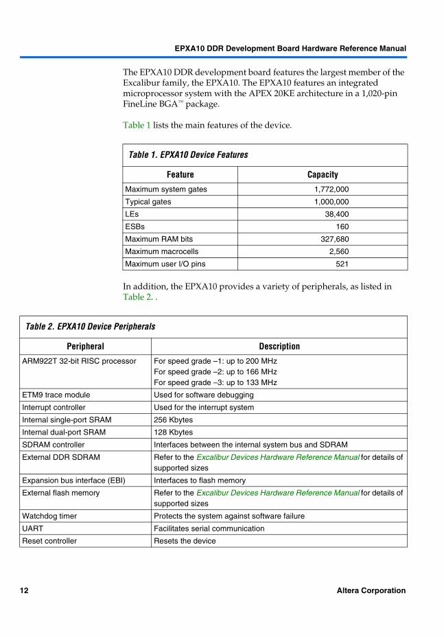
EPXA10 DDR Development Board Hardware Reference Manual
Figure 11 Clock Generators on the EPXA10 DDR development Board
CLK_REF amp the FPGA Clocks
The reference clock for the EPXA10 embedded stripe (CLK_REF) uses a zero-delay clock buffer to allow a 33-V to 5-V interface as well as buffering the clock signal
The four FPGA clocks service the ClockLocktrade and ClockBoosttrade circuitry on the Excalibur device They go through a MAX 3032 device to give 5-V compatibility and to act as a buffer
Altera Corporation 37
EPXA10 DDR Development Board Hardware Reference Manual
MAX 3032
The Altera MAX 3032 is a PLD that is used in this design as an economic method of delivering maximum flexibility for the clock distribution on the EPXA10 DDR development board It allows you to use 5-V clock input signals using DIL14 sockets or SMA connectors Control signals have been added to the PLD to give some extra flexibility if for example the clock input signal needs to be sequenced or stopped
On the EPXA10 DDR development board the MAX 3032 is programmed using minimal logicmdashall clocks use straight connections from input to output as does the reset signal The only logic used in the MAX 3032 is a tri-state buffer to held NSTATUS and prevent any power-up sequencing problem
Figure 12 shows the connections on the MAX 3032 device
Figure 12 Block Diagram Showing MAX 3032 Connections
Embedded Stripe Clocks
Table 29 on page 39 lists the clocks on the EPXA10 device and their sources on the development board
The clocks on the development board can be configured as required depending on which devices are used
MAX 3032
CLK1_IN
CLK2_IN
PCI_CLK_IN
CLK4_IN
NRESET
GLOBNRS_IN
IO1
IO3
IO2
CLK1
CLK2
PCI_CLK
CLK4
GLOBNRS
IO_CLKUSR
IO2MAX
INIT_DONE
CONF_DONE
38 Altera Corporation
EPXA10 DDR Development Board Hardware Reference Manual
Table 29 EPXA10 DDR development Board Clock Sources
EPXA10 Pin Name
EPXA10 Pin Number
Board Connection
Description Test Point
CLK_REF A28 STRIPE_CLK 50-MHz main clock provided to the synchronous memory and embedded processor Dedicated input
TP_CLK_REF
CLK1 N30 CLK1_INMAX303225JP3
12-MHz clock input TP_CLK1
CLK2 Y3 CLK2_INMAX303228JP8
25-MHz clock input TP_CLK2
CLK3 W30 JP9PCI_CLK_IN
32-MHz clock input TP_CLK3
CLK4 P3 CLK4_INMAX303222
48-MHz clock input TP_CLK4
IOCLK1A V30 NCLK1 Clock input in LVDS mode TP_NCLK1
IOCLK2A R3 NCLK2 Clock input in LVDS mode TP_NCLK2
IOCLK3A Y30 NCLK3 Clock input in LVDS mode TP_NCLK3
IOCLK4A N3 NCLK4 Clock input in LVDS mode TP_NCLK4
IOCLKFBIN1A AM28 NCLK1_FB Dedicated pin that allows external feedback to the PLL in LVDS mode
TP_NCLK1_FB
IOCLKFBIN2A J3 NCLK2_FB Dedicated pin that allows external feedback to the PLL in LVDS mode
TP_NCLK2_FB
IOLOCKOUT0 AC30 U1683 Status of ClockLock PLL1
IOLOCKOUT1 AK4 U168 Status of ClockLock PLL2
IOLOCKOUT2 H30 U1685 Status of ClockLock PLL3
IOLOCKOUT3 AK5 U163 Status of ClockLock PLL4
PLLENABL P30 U1683 Dedicated pin used for PLL circuitry
CLKOUT0 AM29 CLK1_OUT Dedicated pin that allows the PLL output to be driven off-chip
TP_CLK1_OUT
CLKOUT1 AH3 CLK2_OUT Dedicated pin that allows the PLL output to be driven off-chip
TP_CLK2_OUT
CLKFBIN0 AL28 CLK1_FBp Dedicated pin that allows external feedback to the PLL
TP_CLK1_FBp
CLKFBIN1 K3 CLK2_FBp Dedicated pin that allows external feedback to the PLL
TP_CLK2_FBp
Altera Corporation 39
EPXA10 DDR Development Board Hardware Reference Manual
Jumper Configuration for the Clock Input
Jumpers JP1 to JP10 are used to select different clock inputs
JP1 JP2 and JP4 to JP6 enable and disable the clocks (X1 X2 and X4 to X6 respectively)
JP3 is used to set CLK1 to oscillator 0 (position 1-2) or to the Ethernet clock TX_CLK (position 2-3)
JP7 enables and disables the Ethernet clock JP8 is used to set CLK2 to oscillator 1 (position 1-2) or to the Ethernet
clock RX_CLK (position 2-3) JP9 and JP10 can be used to connect CLK3 to lvdstxinclk1p and
NCLK3 to lvdstxclk1n respectively
During development if you need to run any of the clocks at a slower or faster rate you can do so using either the external clock input or a variable oscillator
Sources for the EPXA10 Clocks
There are three options for providing a source for the EPXA10 stripe clocks
External clock generator Main clock An alternative crystal oscillator
Using an External Clock Generator
To select the external clock generator for a clock input set the appropriate jumper to position 1-2 to disable the main clock
Using the Main Clock
To use the main clock for a clock input set the appropriate jumper to position 2-3 to enable the crystal oscillator
Using a Variable Oscillator
To use a variable oscillator as a clock input follow the steps below
1 Plug in the DIL14 crystal oscillator package to the appropriate socket
2 Disable the relevant main clock by connecting pins 1 and 2 of the appropriate jumper (see Table 26 on page 34)
40 Altera Corporation
EPXA10 DDR Development Board Hardware Reference Manual
3 Provide a 5-V power supply on the board either by connecting the ATX power supply or by connecting an alternative 5-V input to JP11
1 The clock buffer and the MAX 3032 are 5-V compatible they convert 5-V input from the crystal oscillator to the 33 V required for the clocksrsquo inputs
Device Configuration
There are three methods of configuring and programming the EPXA10 device
Booting from flash memory Configuring the device from the EPC16 Using the Quartusreg II software to configure the device using the
JTAG interface
1 On the EPXA10 device the settings of BOOT_FLASH MSEL0 and MSEL1 determine the configuration mode and method See Figure 10 on page 33 for their location on the EPXA10 DDR development board
See ldquoJTAG Interfacesrdquo on page 45 for more details about using a JTAG interface
Booting from Flash Memory
The Altera flash memory programmer (exc_flash_programmerexe) is a utility that allows you to program flash memory on the EBI using the JTAG interface and the ByteBlasterMV or MasterBlaster download cable
After reset the processor boots up and executes the bootloader from flash memory The bootloader configures the stripe loads the user software into memory configures the FPGA side of the EPXA10 and then begins to execute the user code
Table 30 summarizes the board jumper requirements for booting from flash memory
f For further details about booting the device from flash memory refer to the Excalibur Devices Hardware Reference Manual
Table 30 Jumper Settings for Booting from Flash Memory
BOOT_FLASH MSEL0 MSEL1 Mode
1 0 0 Boot from 16-bit flash
Altera Corporation 41
EPXA10 DDR Development Board Hardware Reference Manual
Configuring Using the EPC16
The Quartus II software can generate a programmer object file (pof) containing both hardware and software for downloading into the EPC16 device on the EPXA10 DDR development board For more details see ldquoEPC16 Configuration Devicerdquo on page 44
1 The EPC16 device can be programmed with the Quartus II software version 11 or higher using either the MasterBlaster or ByteBlasterMV download cables
Table 31 summarizes the jumper requirements for booting your system from an EPC16
When power is applied to the development board the EPC16 configuration device loads configuration data into the EPXA10 device if it has been programmed If you change the configuration devicersquos programming information you must turn the board off and on before new information can be loaded into the EPXA10 device
The EPC16 device can be programmed through the JTAG interface see ldquoEPC16 Configuration Devicerdquo on page 44
To configure the device using the EPC16 device start the Quartus II software and specify the EPC16 as an output option to create the required pof files If the EPC16 is not specified the Quartus II software generates a single file to program the EPXA10 device directly
When configuring an Excalibur device using the EPC16 configuration device some simple logic must be placed in the system to allow both the Excalibur and EPC16 devices to fully come out of reset before any configuration begins
During a configuration the EPC16 uses the signals OE (connected to nSTATUS on the Excalibur device) and nCS (connected to CONF_DONE on the Excalibur device) to determine what action it should take
Table 31 Jumper Settings for Booting from a Serial Device
BOOT_FLASH MSEL0 MSEL1 Mode
0 0 0 Serial
42 Altera Corporation
EPXA10 DDR Development Board Hardware Reference Manual
In its long power-on-reset (POR) mode the EPC16 begins sampling CONF_DONE and OE approximately 100 ms after power-up If the Excalibur device is still in POR after this 100 ms the signals from the Excalibur device that control the state of the EPC16 could be in an unknown state when the EPC16 begins sampling them which results in indeterminate behavior Therefore you must provide logic to hold these signals low until the Excalibur devicersquos nRESET signal is deasserted By holding nSTATUS and OE low the reset of the EPC16 can be extended until the Excalibur device has also come out of POR By holding CONF_DONE and nCS low the EPC16 does not erroneously sample it as being high which falsely indicates that the Excalibur device has already been configured Because both signals are open-drain they can safely be driven low by external logic without causing contention Once nRESET goes high the Excalibur device is ready and the signals can be tri-stated by the external logic to operate normally As opposed to nPOR nRESET deasserts some time after the Excalibur device comes out of POR For this reason use the nRESET signal not NPOR to control the tri-stating of nSTATUS and CONF_DONE to provide a margin of safety Figure 13 shows the circuit that accomplishes the reset dependency requirements
Figure 13 Reset Dependency Circuit
Configuring Using JTAG
The Quartus II software can generate an SRAM object file (sof) containing both hardware and software
The Quartus II programmer uses the sof file to configure the EPXA10 device via JTAG using either the MasterBlaster or ByteBlasterMV download cables For more details see ldquoMasterBlasterByteBlasterMV Communications Cablerdquo on page 44
For further details of how to create a sof file and configure the EPXA10 device via JTAG consult the Quartus II Help
Table 32 summarizes the jumper requirements for booting your system from an EPC16
CONF_DONE and nCS
nSTATUS and OE
nRESET
Altera Corporation 43
EPXA10 DDR Development Board Hardware Reference Manual
Configuration Schemes
Table 33 lists the serial configuration schemes that are available for the EPXA10 device
EPC16 Configuration Device
The EPC16 is part of the on-board JTAG chain that allows in-system programming The device is an EPC16 88-pin Ultra FineLine BGA it contains reprogrammable flash memory to use for serial device configuration For more details about configuring these devices refer to the data sheet Configuration Devices for ACEX APEX FLEX amp Mercury Devices
f For signal details of the EPC16 device refer to the EPC16 pin-out table
MasterBlasterByteBlasterMV Communications Cable
The ByteBlasterMV and MasterBlaster cables have a 10-pin header for use with the development board The cable allows you to download hardware and software configuration data directly to the EPXA10 device or to the EPC16 configuration device The development board supports only JTAG download mode not passive serial download mode The MasterBlaster and ByteBlasterMV cables also support in-circuit hardware debugging with the SignalTapreg embedded logic analyzer
1 The MasterBlaster cable can also be used in conjunction with the ARM debugger to debug your software using JTAG
Debugging Features
On the EPXA10 DDR development board a variety of debugging tools both Altera and third-party products can be used in conjunction with the JTAG interfaces to debug systems under development
Table 32 Jumper Settings for Configuring Using JTAG
BOOT_FLASH MSEL0 MSEL1 Mode
1 0 0 Serial
Table 33 Supported Serial Configuration Schemes
Configuration Scheme Data Source
Configuration device EPC16 configuration device
JTAG MasterBlasterByteBlasterMV download cable
44 Altera Corporation
EPXA10 DDR Development Board Hardware Reference Manual
Third-Party Debugging Tools
Third-party debugging tools such as Lauterbach and the GNUPro XRAY debugger can be used with the EPXA10 DDR development board For latest details of which tools are available access the Altera website at httpwwwAlteracom
JTAG Interfaces
There are three JTAG interfaces on the EPXA10 DDR development board
The MB_BLASTER connector is used to connect an Altera ByteBlaster or MasterBlaster download cable
The MULTI_ICE connector is used to connect a Multi-ICE cable or any other compatible cable
The TRACE_PORT connector is used to connect a trace capture unit or logic analyzer
The MB_BLASTER connector can be used with both the flash programmer and the Quartus programmer using the ByteBlasterMV and MasterBlaster cables and can be used to program the EPC16 The MasterBlaster and ByteBlasterMV cables also support in-circuit hardware debugging on the MB_BLASTER connector using the SignalTapreg embedded logic analyzer The JSELECT setting does not affect these functions
Using JSELECT
The JSELECT jumper determines whether a JTAG debugger can be connected to the MB_BLASTER connector the MULTI_ICE connector or the TRACE_PORT connector shows the JSELECT settings required
Table 34 Using JSELECT to Select a Debugging Connector
Debugger JSELECT Value
Altera-RDI via a ByteBlasterMV or MasterBlaster cable lsquo1rsquo
Multi-ICE or a compatible device on the Multi-ICE connector lsquo0rsquo
Trace port connector or a compatible device on the trace port connector
lsquo0rsquo
Altera Corporation 45
EPXA10 DDR Development Board Hardware Reference Manual
1 Damage can result if you simultaneously connect a device that drives the JTAG pins on the trace port connector and another device on the Multi-ICE connector
You can simultaneously connect one device to the MB_BLASTER connector and another to one of the other two connectors or you can connect devices to the trace port and Multi_ICE connectors at the same time providing that the device on the trace port connector does not drive the JTAG pins on that connector
Using MasterBlasterByteBlasterMV Cable to Program the EPC16 Device
The EPC16 device can be programmed using the Quartus II software version 11 or higher using either the MasterBlaster or ByteBlasterMV download cable
Figure 14 on page 47 shows how the MasterBlaster ByteBlasterMV and Multi-ICE cables are connected
46 Altera Corporation
EPXA10 DDR Development Board Hardware Reference Manual
Figure 14 Connecting the MasterBlaster ByteBlasterMV or Multi-ICE Cables
Power Supply
The EPXA10 DDR development board can be powered by either a laboratory bench power supply or a commercially-available PC-style power supply (ATX) The bench supply provides 33-V the ATX supply provides voltage levels of plusmn12 V plusmn5 V and +33 V The development board derives VTT (125-V) VREF (125-V) +25-V and +18-V supplies from the input power supply If there are no devices attached to the PCI connectors only the 33-V supply input is necessary but to use devices on the PCI connectors you need an ATX power supply to provide the different voltages
1 Ensure that the voltage setting on the ATX power supply is set to the appropriate voltage based on the AC power outlet supply
Figure 15 on page 48 shows the location of the power supply inputs for the EPXA10 DDR development board
Multi_ICE
JSELECT
MB Blaster
EPXA10Device
Development Board
10 24
135
68
79102 4
1 3
20
5
6 8 12 14 16 18
7 9 11 13 15 17 19
123456789
10
TCKGNDTDOVCCTMSVIOTCKNCTDIGND
123456789
1011121314151617181920
VCCVCCPROC_NTRSTGNDPROC_TDIGNDPROC_TMSGNDPROC_TCKGNDGNDGNDPROC_TDOGNDNSRSTGNDNCGNDNCGND
Altera Corporation 47
EPXA10 DDR Development Board Hardware Reference Manual
Figure 15 EPXA10 Power Supply Inputs
1 See Figure 1 on page 11 to see the development board layout in greater detail
A status LED is provided for each power supply source see Table 19 on page 24
5 V
33 V
GND
GNDNC
20
111
10
2019181716151413121110
987654321
5 V5 V-5 VGNDGNDGNDmain switchGND-12 V33 V12 VNCPWR_OKGND5 VGND5 VGND33 V33 V
48 Altera Corporation
EPXA10 DDR Development Board Hardware Reference Manual
1 The total current that can be drawn depends on the daughter card power supply as follows 1 A for 33 V 5 V or 12 V and 100 mA for ndash12 V This can be drawn from a single pin but designers should use as many of pins available on the header as possible to ease the power distribution on the daughter card
Tables 35 through 40 list the estimated power requirements for the development board
Table 35 plusmn120-V Supply Requirements
Module mA (12 V) mA (ndash12 V)
PCIs 500 100
Table 36 50-V Supply Requirements
Module mA (5 V)
PCI Depends on system
CLK_REF Alternative crystal oscillator
CLK1 5
CLK2 5
CLK3 5
CLK4 5
ATX PSU 1000 (to provide adequate regulation)
Table 37 33-V Supply Requirements
Module mA (33 V)
EPXA10 IO Depends on application
Flash memory 300
PCIs 76A (system-dependent)
UARTs 50
Ethernet -
LEDs 20 times 22
EPC16 50
Crystal oscillator 15 times 5
Power-on reset 10
Clock buffers 32 times 2
Altera Corporation 49
EPXA10 DDR Development Board Hardware Reference Manual
Table 38 25-V Supply Requirements
Module mA (25 V)
DDR SDRAM 500 mA
Table 39 18-V Supply Requirements
Module mA (18 V)
EPXA10 device core Depends on application
Table 40 125-V Supply Requirements
Module mA (125 V)
VTT 1500
VREF 25
50 Altera Corporation
EPXA10 DDR Development Board Hardware Reference Manual
Test Points Table 41 on page 51 lists the test points on the EPXA10 DDR development board
Table 41 EPXA10 DDR development Board Test Points
Test Point Connected To Test Point Connected To
GND1 GND TP_NCLK1_FB NCLK1_FB
GND2 GND TP_NCLK2_FB NCLK2_FB
GND3 GND TP_CS0_N CS0_N
GND4 GND TP_CS1_N CS1_N
GND5 GND TP_CS2_N CS2_N
GND6 GND TP_CS3_N CS3_N
GND7 GND TP_EBI_CLK EBI_CLK
TP_CLK_REF CLK_REF TP_OE_N OE_N
TP_CLK1 CLK1 TP_WE_N WE_N
TP_CLK2 CLK2 TP_TCK TCK
TP_CLK3 CLK3 TP_TDI TDI1
TP_CLK4 CLK4 TP_TDO TDO1
TP_CLK1_FBP CLK1_FBP TP_TMS TMS1
TP_CLK1_OUT CLK1_OUT ndash12V Test points for input power supplyTP_CLK2_FBP CLK2_FBP ndash5V
TP_CLK2_OUT CLK2_OUT 18V
TP_NCLK1 NCLK1 12V
TP_NCLK2 NCLK2 25V
TP_NCLK3 NCLK3 33V
TP_NCLK4 NCLK4 5V
U34 ATX POWER_OK
Altera Corporation 51
EPXA10 DDR Development Board Hardware Reference Manual
Signals Tables 42 through 46 document the signals for the following peripherals
UART PCI card Trace port Configurationdebugging interfaces
UART
Figure 16 shows the UART DB9 male connector used on the development board
Figure 16 DTE UART DB9 Male Connector
Table 42 lists the UART DB9 signals
Note(1) The EPXA10 DDR development board has two DB9 male connectors
See Table 53 on page 64 for UART pin-out information
1 2 3 4 56 7 8 9
Table 42 DTE UART DB9 Male Connector Signals Note (1)
Pin Signal Description
1 DCD Data carrier detect
2 RXD Receive data
3 TXD Transmit data
4 DTR Data terminal ready
5 GND Signal ground
6 DSR Data set ready
7 RTS Request to send
8 CTS Clear to send
9 RI Ring indicator
52 Altera Corporation
EPXA10 DDR Development Board Hardware Reference Manual
PCI
Table 43 lists the PCI connector signals used on the development board
See Table 52 on page 63 for pin-out information for the PCI connectors
Table 43 PCI Card 33-V-Only Connector
Pin Signal Pin Signal Pin Signal Pin SIgnal
A1 TRST A2 +12 V B1 ndash12 V B2 TCK
A3 TMS A4 TDI B3 GND B4 TDO
A5 +5 V A6 INTA B5 +5 V B6 +5 V
A7 INTC A8 +5 V B7 INTB B8 INTD
A9 RESERVED A10 V IO B9 PRSNT1 B10 RESERVED
A11 RESERVED A12 RESERVED B11 PRSNT2 B12 RESERVED
A13 RESERVED A14 33 V AUX B13 RESERVED B14 RESERVED
A15 RST A16 V IO B15 GND B16 PCI_CLK
A17 V IO A18 GNT1 B17 GND B18 REQ1
A19 GND A20 AD [30] B19 V IO B20 AD [31]
A21 + 33 V A22 AD [28] B21 AD [29] B22 GND
A23 AD [26] A24 GND B23 AD [27] B24 AD [25]
A25 AD[24] A26 IDSEL B25 VCC B26 CBE3
A27 + 33 V A28 AD[22] B27 AD[23] B28 GND
A29 AD[20] A30 GND B29 AD[21] B30 AD[19]
A31 AD[18] A32 AD[16] B31 VCC B32 AD[17]
A33 + 33 V A34 FRAME B33 CBE2 B34 GND
A35 GND A36 TRDY B35 IRDY B36 + 33 V
A37 GND A38 STOP B37 DEVSEL B38 GND
A39 + 33 V A40 RESERVED B39 LOCK B40 PERR
A41 RESERVED A42 GND B41 + 33 V B42 SERR
A43 PAR A44 AD[15] B43 + 33 V B44 CBE1
A45 + 33 V A46 AD[13] B45 AD[14] B46 GND
A47 AD[11] A48 GND B47 AD[12] B48 AD[10]
A49 AD[9] A50 GND B49 M66EN B50 GND
A51 GND A52 CBE0 B51 GND B52 AD[8]
A53 + 33 V A54 AD[6] B53 AD[7] B54 + 33 V
A55 AD[4] A56 GND B55 AD[5] B56 AD[3]
A57 AD[2] A58 AD[0] B57 GND B58 AD[1]
A59 V IO A60 REQ64 B59 + 33 V B60 ACK64
A61 + 5 V A62 + 5 V B61 + 5 V B62 + 5 V
Altera Corporation 53
EPXA10 DDR Development Board Hardware Reference Manual
Trace Port
Table 44 lists the ETM9 trace port signals
See Table 57 on page 66 for pin-out information for the ETM9 trace port
Table 44 Trace Port Signals
Pin Signal Description Pin Signal Description
1 NC No connection 2 NC No connection
3 NC No connection 4 NC No connection
5 GND Ground 6 TRACECLK Clock output for the trace port
7 DBGRQ Not used 8 DBGACK Output (not used)
9 nSRST System reset detector 10 EXTTRIG Output (not used)
11 TDO Test data input 12 VTRef Reference voltage input
13 RTCK Input (not used) 14 VSupply Power input for the debug equipment
15 TCK Test clock output 16 TRACEPKT7 Dataaddress information output on pipeline status17 TMS Test mode select output 18 TRACEPKT6
19 TDI Test data output 20 TRACEPKT5
21 nTRST Reset inputoutput 22 TRACEPKT4
23 TRACEPKT15 Dataaddress information output on pipeline status
24 TRACEPKT3
25 TRACEPKT14 26 TRACEPKT2
27 TRACEPKT13 28 TRACEPKT1
29 TRACEPKT12 30 TRACEPKT0
31 TRACEPKT11 32 TRACESYNC
33 TRACEPKT10 34 PIPESTAT2 Processor pipeline status
35 TRACEPKT9 36 PIPESTAT1
37 TRACEPKT8 38 PIPESTAT0
39 GND Ground 40 GND Ground
41 GND Ground 42 GND Ground
43 GND Ground
54 Altera Corporation
EPXA10 DDR Development Board Hardware Reference Manual
ConfigurationDebugging Interfaces
On the development board there are interfaces for a MasterBlaster or ByteBlasterMV cable and a Multi-ICE connector Table 45 lists the signals on the MasterBlasterByteBlasterMV interface
See Table 47 on page 58 for pin-out information for the development board configuration and debugging interfaces
Table 45 MasterBlasterByteBlasterMV Female Interface
Pin JTAG Mode
Signal Description
1 TCK Clock signal
2 GND Signal ground
3 TDO Data from device
4 Vcc Power supply
5 TMS JTAG state machine control
6 Vio Reference voltage for MasterBlasterByteBlasterMV output driver
7 TCK Clock signal
8 ndash No connection
9 TDI Data to device
10 GND Signal ground
Altera Corporation 55
EPXA10 DDR Development Board Hardware Reference Manual
Table 46 lists the signals on the Multi-ICE interface
See Table 47 on page 58 for pin-out information for the development board configuration and debugging interfaces
f For signal details of the EPC16 device refer to the EPC16 pin-out table
See Table 57 on page 66 for pin-out information for the trace port
Table 46 Multi-ICE Connector
Pin Signal Description Direction
1 Vcc Power supply NA
2 Vcc Power supply NA
3 PROC_NTRTS Processor reset O
4 GND Ground NA
5 PROC_TDI Processor test data input I
6 GND Ground NA
7 PROC_TMS Processor test mode select I
8 GND Ground NA
9 PROC_TCK Processor test clock input I
10 GND Ground NA
11 GND Ground NA
12 GND Ground NA
13 PROC_TDO Processor test data output O
14 GND Ground NA
15 NSRST Warm reset IO
16 GND Ground NA
17 NC No connection NA
18 GND Ground NA
19 NA No connection NA
20 GND Ground NA
56 Altera Corporation
EPXA10 DDR Development Board Hardware Reference Manual
Pin-Outs The main component of the development board is the EPXA10F1020C1 device The pins on the EPXA10 device are assigned to functions on the board When generating IP cores for the EPXA10 device the pins must be used as defined to avoid damaging the device and any unused pins must be tri-stated using the Quartus II software The following sections list the interfaces and dedicated pins on the board Any pins not used for a design should be left in the high-impedance (input) state to avoid contention
This section details the EPXA10 device pins that are assigned to the following purposes
Configuration DDR SDRAM EBI UARTs 1 and 2 Ethernet User LEDs push buttons and dip-switches Fast IO pins IDC 10-pin header Trace port Test points
Pin assignments are grouped into tables for control pins bank address pins and data bus pins where appropriate The tables also detail signals passing across a connection The remaining IO pins on the EPXA10 device are listed at the end of this section
Configuration
The EPXA10 device pins listed in Table 47 on page 58 are used exclusively for configuring the device Refer to ldquoDevice Configurationrdquo on page 41 for more information about EPXA10 configuration
Altera Corporation 57
EPXA10 DDR Development Board Hardware Reference Manual
Table 47 EPXA10 Device Configuration Pins
Signal Name EPXA10 Device Pin Description
MSEL0 J30 Configuration mode select (tied to GND)
MSEL1 K30 Configuration mode select (tied to GND)
NSTATUS AM14 OE for EPC16
NCONFIG R30 n_INIT_CONF for EPC16
DCLK W3 Data clock for EPC16
CONF_DONE AM13 Configuration complete indicator
INIT_DONE D14 Initialization complete indicator
nCE AC3 Not connected
nCEO D13
DATA0 V3 Serial input for EPC16 configuration data
DATA1 D10 Serial input for EPC16 configuration data available for user IO after configurationDATA2 A9
DATA3 B9
DATA4 C9
DATA5 D9
DATA6 A4
DATA7 B4
TDI AD3 JTAG data input
TDO E11 JTAG data output (to next device in the chain
TCK AM19 JTAG clock
TMS AM20 JTAG mode select
TRST C13 JTAG reset (pulled high)
PROC_TDI H27 JTAG data input
PROC_TDO H26 JTAG data output (to next device in the chain
PROC_TCK D30 JTAG clock
PROC_TMS E29 JTAG mode select
PROC_TRST E30 JTAG reset (pulled high)
DEV_CLRn H3 Global reset for the device
DEV_OE AE3 Device output enable
nWS C4 Write strobe
nRS D4 Read strobe
nCS D3 Signal providing handshaking between devices
CS E3 Chip select
RDYnBSY E14 Readybusy
CLKUSR A13 Clock signal
58 Altera Corporation
EPXA10 DDR Development Board Hardware Reference Manual
DDR SDRAM Interface
There are four DDR chips (256-Mbit times 8) on the EPXA10 DDR development board selectable using one chip-select SD_CS0_N The development board DDR interface can run at up to 266 MHz
f For more details on how to use the DDR SDRAM ref to AN141 Using the SDRAM Controller
Table 48 lists the pin-outs for the DDR SDRAM control signals
Table 49 on page 60 lists the DDR SDRAM data bank and address bus pin-outs
Table 48 DDR SDRAM Control Signal Pin-Outs
Signal Name EPXA10 Device Pin Description
SD_RAS_N F17 Row address strobe
SD_CAS_N F18 Column address strobe
SD_WE_N G18 Write enable
SD_CS0_N G14 Chip select
SD_CS1_N F16 Chip select
SD_CLKE F14 Clock enable
SD_CLK F15 SDRAM clock
SD_CLK_N G13 SDRAM clock - inverted
SD_DQM(0) H14 Data byte mask
SD_DQM(1) L14 Data byte mask
SD_DQM(2) K9 Data byte mask
SD_DQM(3) H9 Data byte mask
SD_DQS(0) J14 DQS signal
SD_DQS(1) K14 DQS signal
SD_DQS(2) K10 DQS signal
SD_DQS(3) H10 DQS signal
Altera Corporation 59
EPXA10 DDR Development Board Hardware Reference Manual
Table 49 DDR SDRAM Data Bank amp Address Bus Pin-Outs
Signal Name EPXA10 Device Pin
Signal Name EPXA10 Device Pin
Signal Name EPXA10 Device Pin
SD_DQ0 H18 SD_DQ1 H17 SD_DQ2 H16
SD_DQ3 J18 SD_DQ4 J17 SD_DQ5 H15
SD_DQ6 J16 SD_DQ7 J15 SD_DQ8 K18
SD_DQ9 K17 SD_DQ10 L18 SD_DQ11 K16
SD_DQ12 L17 SD_DQ13 L16 SD_DQ14 K15
SD_DQ15 L15 SD_DQ16 L13 SD_DQ17 K13
SD_DQ18 L12 SD_DQ19 K12 SD_DQ20 L11
SD_DQ21 K11 SD_DQ22 L10 SD_DQ23 L9
SD_DQ24 H13 SD_DQ25 H12 SD_DQ26 J13
SD_DQ27 J12 SD_DQ28 J11 SD_DQ29 J10
SD_DQ30 J9 SD_DQ31 H11 SD_ADD0 G12
SD_ADD1 F13 SD_ADD2 G11 SD_ADD3 F12
SD_ADD4 F11 SD_ADD5 G10 SD_ADD6 F10
SD_ADD7 F9 SD_ADD8 G9 SD_ADD9 F8
SD_ADD10 G8 SD_ADD11 F7 SD_ADD12 F6
SD_ADD13 G7 SD_ADD14 G6
60 Altera Corporation
EPXA10 DDR Development Board Hardware Reference Manual
EBI
Table 50 lists the EPXA10 pin-outs for the EBI control signals
Table 50 EBI Control Signal Pin-Outs
Signal Name EPXA10 Device Pin Description
EBI_BE0 F27 Byte enable
EBI_BE1 E27 Byte enable
EBI_OE F26 Output enable
EBI_WE E26 Write enable
EBI_CS0 A25 Chip select
EBI_CS1 B25 Chip select
EBI_CS2 C25 Chip select
EBI_CS3 D25 Chip select
EBI_CLK E25 EBI clock
EBI_ACK F25 EBI acknowledge
INT_EXTPIN_N G25 Interrupt generated by push-button SW4
Altera Corporation 61
EPXA10 DDR Development Board Hardware Reference Manual
Table 51 lists the EBI data bank and address bus pin-outs
Table 51 EBI Data Bank and Address Bus Pin-Outs
Signal Name EPXA10 Device Pin
Signal Name EPXA10 Device Pin
EBI_DQ0 J21 EBI_DQ1 H21
EBI_DQ2 E20 EBI_DQ3 F20
EBI_DQ4 E19 EBI_DQ5 L20
EBI_DQ6 K20 EBI_DQ7 J20
EBI_DQ8 H20 EBI_DQ9 G20
EBI_DQ10 F19 EBI_DQ11 G19
EBI_DQ12 L19 EBI_DQ13 K19
EBI_DQ14 J19 EBI_DQ15 H19
EBI_A0 H25 EBI_A1 D24
EBI_A2 E24 EBI_A3 F24
EBI_A4 G24 EBI_A5 J24
EBI_A6 H24 EBI_A7 E23
EBI_A8 F23 EBI_A9 G23
EBI_A10 K23 EBI_A11 J23
EBI_A12 H23 EBI_A13 E22
EBI_A14 F22 EBI_A15 E21
EBI_A16 L22 EBI_A17 K22
EBI_A18 J22 EBI_A19 H22
EBI_A20 G22 EBI_A21 F21
EBI_A22 G21 EBI_A23 L21
EBI_A24 K21
62 Altera Corporation
EPXA10 DDR Development Board Hardware Reference Manual
PCI
Table 52 lists the pins used for the PCI cards
Table 52 PCI Pin-Outs
FPGA UART Embedded Stripe UART
EPXA10 Device Pin
Device Signal (Board Signal)
EPXA10 Device Pin
Device Signal (Board Signal)
AF21 CBE0 AF22 A5 (PCI_BUS5)
AE19 CBE1 AG22 A6 (PCI_BUS6)
AF19 CBE2 AH22 A7 (PCI_BUS7)
AJ18 CBE3 AD21 A8 (PCI_BUS8)
AG19 DEVSEL AE21 A9 (PCI_BUS9)
AH19 FRAME AG21 A10 (PCI_BUS10)
AB20 GNT1 AH21 A11 (PCI_BUS11)
AC20 GNT2 AD20 A12 (PCI_BUS12)
AB22 INTA AE20 A13 (PCI_BUS13)
AG23 INTB AF20 A14 (PCI_BUS14)
AC22 INTC AH20 A15 (PCI_BUS15)
AF23 INTD AJ19 A16 (PCI_BUS16)
AK20 PAR AK19 A17 (PCI_BUS17)
AB18 PCI_RST AL19 A18 (PCI_BUS18)
AL18 PERR AD18 A19 (PCI_BUS19)
AB21 PRSNT1 AE18 A20 (PCI_BUS20)
AC22 PRSNT2 AF18 A21 (PCI_BUS21)
AD19 REQ1 AG18 A22 (PCI_BUS22)
AC19 REQ2 AH18 A23 (PCI_BUS23)
AB19 SERR AK18 A24 (PCI_BUS24)
AB17 STOP AC17 A25 (PCI_BUS25)
AC18 TRDY AD17 A26 (PCI_BUS26)
AK23 A0 (PCI_BUS0) AE17 A27 (PCI_BUS27)
AL23 A1 (PCI_BUS1) AF17 A28 (PCI_BUS28)
AM23 A2 (PCI_BUS2) AG17 A29 (PCI_BUS29)
AD22 A3 (PCI_BUS3) AH17 A30 (PCI_BUS30)
AE22 A4 (PCI_BUS4) AJ17 A31 (PCI_BUS31)
Altera Corporation 63
EPXA10 DDR Development Board Hardware Reference Manual
UART1 amp UART2
Table 53 lists the pins used for UARTs 1 and 2
Ethernet
Table 53 lists the pins used for the Ethernet interface
Table 53 Extension Header UARTs 1 amp 2 IO Pin-Outs
FPGA UART Embedded Stripe UART
EPXA10 Device Pin
Device Signal Expansion Board Connector
EPXA10 Device Pin
Device Signal Expansion Board Connector
J27 UART2_DTR_N U16171 G28 UART1_CTS_N NC
J29 UART2_TXD U16174 D29 UART1_RXD NC
K29 UART2_RXD_N U16177 E28 UART1_RI_N NC
K27 UART2_DSR_N U16179 C28 UART1_RTS_N NC
J28 UART2_RTS_N U16173 F28 UART1_DSR_N NC
J26 UART2_RI_N U16175 G27 UART1_DCD_N NC
K28 UART2_DCD_N U16178 D28 UART1_TXD NC
K26 UART2_CTS_N U16181 G26 UART1_DTR_N NC
Table 54 Extension Header Ethernet Pin-Outs
EPXA10 Device Pin
Device Signal Expansion Board Connector
EPXA10 Device Pin
Device Signal Expansion Board Connector
R23 RXD1 U16155 R24 TXD3 U16153
R25 TXD0 U16149 M19 MDC U16145
M20 RST_N U16146 M21 TX_ER U16161
M22 TX_EN U16162 M23 RXD2 U16157
N19 CRS U16166 N20 COL U16163
N21 RX_DV U16167 N22 MDIO U16169
N23 RXD0 U16154 P20 INTR U16147
P21 RX_ER U16165 P22 RX_D3 U16158
N25 TXD1 U16150 P25 TXD2 U16151
64 Altera Corporation
EPXA10 DDR Development Board Hardware Reference Manual
Fast IO Pins
Table 55 lists the pins used for the EPXA10 fast IO pins
User LEDs Switches amp Push Button Switches
Table 56 lists the pins used for the user-defined LEDs push-button switches and dip-switches
Table 55 EPXA10 Fast IO Pins
EPXA10 Pin Name
Description EPXA10 Device Pin
Expansion Board Connector
Board Reference
FAST0 Dedicated fast IO pins E13 U16133 FAST0
FAST1 Dedicated fast IO pins E12 U16134 FAST1
FAST2 Dedicated fast IO pins AM18 U16135 FAST2
FAST3 Connected to PCI to provide IRDY AM15 IRDY
Table 56 Expansion Header LED Switch and Push Button IO Pin-Outs
EPXA10 Device Pin
Device Signal Expansion Board Connector
EPXA10 Device Pin
Device Signal Board Connector
V6 USER_LED0 U181 U5 USER_LED1 U183
V5 USER_LED2 U184 U6 USER_LED3 U185
V7 USER_LED4 U187 V8 USER_LED5 U188
U7 USER_LED6 U189 T6 USER_LED7 U1811
U8 USER_SW0 U1812 T5 USER_SW1 U1813
V4 USER_SW2 U1815 V10 USER_SW3 U1816
T7 USER_SW4 U1817 W12 USER_SW5 U1817
U9 USER_SW6 U1820 V11 USER_SW7 U1821
R6 USER-SW8 U1823 T8 USER_PB0 U1824
R5 USER_PB1 U1825 U4 USER_PB2 U1827
U10 USER_PB3 U1828
Altera Corporation 65
EPXA10 DDR Development Board Hardware Reference Manual
Trace Port
Table 57 lists the pins used on the trace port interface
IDC 10-Pin Header
Table 56 lists the pins used for the 10-pin IDC header
Table 57 Trace Port Pin-Out
EPXA10 Device Pin
Device Signal EPXA10 Device Pin
Device Signal
H6 TRACEPKT15 N7 TRACEPKT4
J6 TRACEPKT14 H8 TRACEPKT3
K6 TRACEPKT13 J8 TRACEPKT2
L6 TRACEPKT12 K8 TRACEPKT1
M6 TRACEPKT11 L8 TRACEPKT0
N6 TRACEPKT10 M8 TRACESYNC
H7 TRACEPKT9 M9 PIPESTAT2
J7 TRACEPKT8 N9 PIPESTAT1
K7 TRACEPKT7 N10 PIPESTAT0
L7 TRACEPKT6 N8 TRACECLK
M7 TRACEPKT5
Table 58 IDC Header Pin-Outs
EPXA10 Device Pin Header Pin Expansion Board Connector
L5 Header11 U1871
K4 Header12 U1872
J4 Header13 U1873
H4 Header14 U1875
K5 Header15 U1876
E4 Header16 U1877
J5 Header17 U1879
H5 Header18 U1880
GND Header19 na
GND Header110 na
66 Altera Corporation
EPXA10 DDR Development Board Hardware Reference Manual
Expansion Header
The pins on the expansion header cards connect to IO pins on the EPXA10 device to ground or to VCC supplies
IO Pin-Outs
Tables 59 to 62 list the pins on the EPXA10 DDR development board expansion header cards that connect to IO pins on the EPXA10 device Some of these pins can optionally be dedicated to the Ethernet UART user LEDs push-button switches and dip-switches
Table 59 Development Board Expansion Header U15 IO Pin-Outs (Part 1 of 2)
U151-50 Device U1551-100 Device U15101-150
Device U15151-200
Device
U151 AB24 U1551 AC23 U15101 GND U15151 Y5
U152 GND U1552 AD23 U15102 W4 U15152 Y8
U153 L24 U1553 AE23 U15103 W5 U15153 GND
U154 L26 U1554 GND U15104 AA6 U15154 Y7
U155 L27 U1555 AL20 U15105 GND U15155 Y4
U156 GND U1556 AJ20 U15106 W8 U15156 B24
U157 AJ29 U1557 AG20 U15107 Y6 U15157 GND
U158 AK29 U1558 GND U15108 W7 U15158 A24
U159 AH28 U1559 AJ30 U15109 GND U15159 D23
U1510 GND U1560 IOData7 U15110 W6 U15160 C23
U1511 AJ28 U1561 IOData6 U15111 AF5 U15161 GND
U1512 AK28 U1562 GND U15112 AE4 U15162 B23
U1513 AH27 U1563 IOData5 U15113 GND U15163 A23
U1514 GND U1564 IOData4 U15114 AD4 U15164 D20
U1515 AH26 U1565 IOData3 U15115 AC4 U15165 GND
U1516 AG26 U1566 GND U15116 AE5 U15166 C20
U1517 AF26 U1567 IOData2 U15117 GND U15167 B20
U1518 GND U1568 IOData1 U15118 AD8 U15168 A20
U1519 AM25(1) U1569 N26 U15119 AA12 U15169 GND
U1520 AL25 U1570 GND U15120 AC9 U15170 D19
U1521 AK25(1) U1571 N29 U15121 GND U15171 C19
U1522 GND U1572 IOCLKUSR U15122 AD5 U15172 B19
U1523 AJ25(1) U1573 IORDYNBSY U15123 AC5 U15173 GND
U1524 AH25 U1574 GND U15124 AD7 U15174 A19
U1525 AG25 U1575 NRS U15125 GND U15175 A18
Altera Corporation 67
EPXA10 DDR Development Board Hardware Reference Manual
U1526 GND U1576 IONWS U15126 AA11 U15176 B18
U1527 AF25 U1577 IONCS U15127 Y12 U15177 GND
U1528 AE25 U1578 GND U15128 AC8 U15178 D18
U1529 AD25 U1579 IOCS U15129 GND U15179 E18
U1530 GND U1580 M25 U15130 AB5 U15180 D17
U1531 AC25 U1580 M26 U15131 AB9 U15181 GND
U1532 AB25 U1581 P27 U15132 AA10 U15182 E17
U1533 AM24 U1582 GND U15133 GND U15183 D16
U1534 GND U1583 M28 U15134 Y11 U15184 E16
U1535 AL24 U1584 NC U15135 AD6 U15185 GND
U1536 AK24 U1585 NC U15136 AA5 U15186 D15
U1537 AJ24 U1586 GND U15137 GND U15187 B15
U1538 GND U1587 NCLK3 U15138 AC7 U15188 A15
U1539 AH24 U1588 GND U15139 AB8 U15189 GND
U1540 AC24 U1589 NCLK4 U15140 Y10 U15190 B14
U1541 AD24 U1590 GND U15141 GND U15191 A14
U1542 GND U1591 CLK2_OUT U15142 W11 U15192 E15
U1543 AE24 U1592 GND U15143 AA8 U15193 GND
U1544 AF24 U1593 NCLK2_FB U15144 AB7 U15194 C14
U1545 AG24 U1594 GND U15145 GND U15195 NCLK1_FB
U1546 GND U1595 CLK2_FBP U15146 AC6 U15196 GND
U1547 AJ23 U1596 GND U15147 W10 U15197 CLK1_FBP
U1548 AH23 U1597 NCLK2 U15148 AA7 U15198 GND
U1549 AB23 U1598 GND U15149 GND U15199 NCLK1
U1550 GND U1599 CLK1_OUT U15150 AB6 U15200 GND
Table 59 Development Board Expansion Header U15 IO Pin-Outs (Part 2 of 2)
U151-50 Device U1551-100 Device U15101-150
Device U15151-200
Device
68 Altera Corporation
EPXA10 DDR Development Board Hardware Reference Manual
Table 60 Development Board Expansion Header U16 IO Pin-Outs (Part 1 of 2)
U161-50 Device U1651-100
Device U16101-150
Device U16151-200
Device
U161 GND U1651 AD2 U16101 IOLVDSDSKW U16151 P25
U162 AE3 U1652 GND U16102 GND U16152 GND
U163 AK5 U1653 AE1 U16103 W32 U16153 R24
U164 GND U1654 AE2 U16104 W31 U16154 N23
U165 AM5 U1655 GND U16105 GND U16155 R23
U166 AL5 U1656 AH1 U16106 V31 U16156 GND
U167 GND U1657 AH2 U16107 V32 U16157 M23
U168 AK4 U1658 GND U16108 GND U16158 P22
U169 AJ3 U1659 AJ1 U16109 R32 U16159 NC
U1610 GND U1660 AJ2 U16110 R31 U16160 GND
U1611 AL4 U1661 GND U16111 GND U16161 M21
U1612 AM4 U1662 B29 U16112 P31 U16162 M22
U1613 GND U1663 A29 U16113 P32 U16163 N20
U1614 D1 U1664 GND U16114 GND U16164 GND
U1615 D2 U1665 AJ32 U16115 N32 U16165 P21
U1616 GND U1666 AJ31 U16116 N31 U16166 N19
U1617 E1 U1667 GND U16117 GND U16167 N21
U1618 E2 U1668 AH31 U16118 K31 U16168 GND
U1619 GND U1669 AH32 U16119 K32 U16169 N22
U1620 H1 U1670 GND U16120 GND U16170 J26
U1621 H2 U1671 AE32 U16121 J32 U16171 J27
U1622 GND U1672 AE31 U16122 J31 U16172 GND
U1623 J1 U1673 GND U16123 GND U16173 J28
U1624 J2 U1674 AD31 U16124 H31 U16174 J29
U1625 GND U1675 AD32 U16125 H32 U16175 UART2_RI_N
U1626 K1 U1676 GND U16126 GND U16176 GND
U1627 K2 U1677 AC32 U16127 E32 U16177 K29
U1628 GND U1678 AC31 U16128 E31 U16178 K28
U1629 N2 U1679 GND U16129 GND U16179 K27
U1630 N1 U1680 Y31 U16130 D31 U16180 GND
U1631 GND U1681 Y32 U16131 D32 U16181 K26
U1632 P1 U1682 GND U16132 GND U16182 L28
U1633 P2 U1683 AC30 U16133 FAST0 U16183 L23
U1634 GND U1684 AL29 U16134 FAST1 U16184 GND
Altera Corporation 69
EPXA10 DDR Development Board Hardware Reference Manual
U1635 R1 U1685 H30 U16135 FAST2 U16185 GND
U1636 R2 U1686 GND U16136 GND U16186 12V
U1637 GND U1687 5V U16137 R26 U16187 33V
U1638 V1 U1688 33V U16138 R27 U16188 12V-
U1639 V2 U1689 5V U16139 R28 U16189 33V
U1640 GND U1690 33V U16140 GND U16190 12V-
U1641 W1 U1691 5V U16141 R29 U16191 33V
U1642 W2 U1692 33V U16142 P28 U16192 12V
U1643 GND U1693 5V U16143 P29 U16193 33V
U1644 Y2 U1694 33V U16144 GND U16194 12V
U1645 Y1 U1695 5V U16145 M19 U16195 33V
U1646 GND U1696 33V U16146 M20 U16196 12V
U1647 AC1 U1697 5V U16147 P20 U16197 33V
U1648 AC2 U1698 33V U16148 GND U16198 12V
U1649 GND U1699 5V U16149 R25 U16199 33V
U1650 AD1 U16100 33V U16150 N25 U16200 12V
Table 60 Development Board Expansion Header U16 IO Pin-Outs (Part 2 of 2)
U161-50 Device U1651-100
Device U16101-150
Device U16151-200
Device
70 Altera Corporation
EPXA10 DDR Development Board Hardware Reference Manual
Table 61 Development Board Expansion Header U17 IO Pin-Outs (Part 1 of 2)
U171-50 Device U1751-100 Device U17101-150
Device U17151-200
Device
U171 AC11 U1751 AJ5 U17101 GND U17151 W22
U172 GND U1752 AH5 U17102 NC U17152 V21
U173 AB11 U1753 AJ4 U17103 NRESET U17153 GND
U174 AH10 U1754 GND U17104 NC U17154 AA28
U175 AJ10 U1755 AH4 U17105 GND U17155 AC27
U176 GND U1756 AG5 U17106 NC U17156 AB26
U177 AK10 U1757 T27 U17107 NC U17157 GND
U178 AL10 U1758 GND U17108 NC U17158 AA25
U179 AG10 U1759 U27 U17109 GND U17159 Y24
U1710 GND U1760 V27 U17110 NC U17160 W23
U1711 AF10 U1761 V26 U17111 NC U17161 GND
U1712 AE10 U1762 GND U17112 NC U17162 V22
U1713 AD10 U1763 T29 U17113 GND U17163 U21
U1714 GND U1764 T28 U17114 AG28 U17164 AB28
U1715 AC10 U1765 T26 U17115 AH29 U17165 GND
U1716 AB10 U1766 GND U17116 AG27 U17166 Y28
U1717 AH9 U1767 U26 U17117 GND U17167 AB27
U1718 GND U1768 W27 U17118 AH30 U17168 AA26
U1719 AJ9 U1769 T25 U17119 AF27 U17169 GND
U1720 AK9 U1770 GND U17120 AF28 U17170 Y25
U1721 AL9 U1771 U25 U17121 GND U17171 V23
U1722 GND U1772 U29 U17122 AE26 U17172 U22
U1723 AM9 U1773 U28 U17123 AE27 U17173 GND
U1724 AG9 U1774 GND U17124 AE30 U17174 T21
U1725 AF9 U1775 R22 U17125 GND U17175 W28
U1726 GND U1776 Y27 U17126 AE29 U17176 W29
U1727 AE9 U1777 W26 U17127 AE28 U17177 GND
U1728 AD9 U1778 GND U17128 AA21 U17178 R20
U1729 AM8 U1779 V25 U17129 GND U17179 T22
U1730 GND U1780 U24 U17130 AD26 U17180 AA27
U1731 AL8 U1781 T23 U17131 AD30 U17181 GND
U1732 AK8 U1782 GND U17132 AD29 U17182 Y26
U1733 AJ8 U1783 R21 U17133 GND U17183 W25
U1734 GND U1784 V29 U17134 AC29 U17184 U23
Altera Corporation 71
EPXA10 DDR Development Board Hardware Reference Manual
U1735 AH8 U1785 V28 U17135 AA22 U17185 GND
U1736 AG8 U1786 GND U17136 AD27 U17186 12V
U1737 AF8 U1787 5V U17137 GND U17187 33V
U1738 GND U1788 33V U17138 AD28 U17188 12V-
U1739 AE8 U1789 5V U17139 Y29 U17189 33V
U1740 AH7 U1790 33V U17140 Y21 U17190 12V-
U1741 AF7 U1791 5V U17141 GND U17191 33V
U1742 GND U1792 33V U17142 AA23 U17192 12V
U1743 AG7 U1793 5V U17143 AC28 U17193 33V
U1744 AE7 U1794 33V U17144 AC26 U17194 12V
U1745 AH6 U1795 5V U17145 GND U17195 33V
U1746 GND U1796 33V U17146 Y22 U17196 12V
U1747 AG6 U1797 5V U17147 W21 U17197 33V
U1748 AF6 U1798 33V U17148 AA24 U17198 12V
U1749 AE6 U1799 5V U17149 GND U17199 33V
U1750 GND U17100 33V U17150 Y23 U17200 12V
Table 61 Development Board Expansion Header U17 IO Pin-Outs (Part 2 of 2)
U171-50 Device U1751-100 Device U17101-150
Device U17151-200
Device
72 Altera Corporation
EPXA10 DDR Development Board Hardware Reference Manual
Table 62 Development Board Expansion Header U18 IO Pin-Outs (Part 1 of 2)
U181-50 Device U1851-100 Device U18101-150
Device U18151-200
Device
U181 V6 U1851 N5 U18101 GND U18151 AF13
U182 GND U1852 R10 U18102 AK17 U18152 AG13
U183 U5 U1853 R11 U18103 AK16 U18153 GND
U184 V5 U1854 GND U18104 AJ16 U18154 AB13
U185 U6 U1855 R12 U18105 GND U18155 AH12
U186 GND U1856 R13 U18106 AH16 U18156 AE12
U187 V7 U1857 P10 U18107 AG16 U18157 GND
U188 V8 U1858 GND U18108 AF16 U18158 AF12
U189 U7 U1859 P11 U18109 GND U18159 AG12
U1810 GND U1860 P12 U18110 AE16 U18160 AG11
U1811 T6 U1861 P13 U18111 AD16 U18161 GND
U1812 U8 U1862 GND U18112 AC16 U18162 AD12
U1813 T5 U1863 P4 U18113 GND U18163 AF11
U1814 GND U1864 N4 U18114 AB16 U18164 AH11
U1815 V4 U1865 N11 U18115 AL15 U18165 GND
U1816 V10 U1866 GND U18116 AK15 U18166 AC12
U1817 T7 U1867 N12 U18117 GND U18167 AE11
U1817 W12 U1868 N13 U18118 AJ15 U18168 AB12
U1818 GND U1869 M5 U18119 AH15 U18169 GND
U1819 USER_SW5 U1870 GND U18120 AG15 U18170 AD11
U1820 U9 U1871 L5 U18121 GND U18171 A8
U1821 V11 U1872 K4 U18122 AF15 U18172 E6
U1822 GND U1873 J4 U18123 AE15 U18173 GND
U1823 R6 U1874 GND U18124 AD15 U18174 E7
U1824 T8 U1875 H4 U18125 GND U18175 C8
U1825 R5 U1876 K5 U18126 AC15 U18176 B8
U1826 GND U1877 E4 U18127 AB15 U18177 GND
U1827 U4 U1878 GND U18128 AL14 U18178 E9
U1828 U10 U1879 J5 U18129 GND U18179 E8
U1829 R7 U1880 H5 U18130 AK14 U18180 D8
U1830 GND U1881 G5 U18131 AJ14 U18181 GND
U1831 V12 U1882 GND U18132 AH14 U18182 B5
U1832 U11 U1883 F5 U18133 GND U18183 A5
U1833 R8 U1884 E5 U18134 AG14 U18184 E10
Altera Corporation 73
EPXA10 DDR Development Board Hardware Reference Manual
GND Connections
Table 59 lists the pins on the EPXA10 DDR development board expansion header cards that connect to GND
U1834 GND U1885 D5 U18135 AF14 U18185 GND
U1835 P6 U1886 GND U18136 AE14 U18186 12V
U1836 T4 U1887 5V U18137 GND U18187 33V
U1837 P5 U1888 33V U18138 AD14 U18188 12V-
U1838 GND U1889 5V U18139 AC14 U18189 33V
U1839 T10 U1890 33V U18140 AB14 U18190 12V-
U1840 U12 U1891 5V U18141 GND U18191 33V
U1841 T11 U1892 33V U18142 AL13 U18192 12V
U1842 GND U1893 5V U18143 AK13 U18193 33V
U1843 P7 U1894 33V U18144 AJ13 U18194 12V
U1844 R9 U1895 5V U18145 GND U18195 33V
U1845 T12 U1896 33V U18146 AH13 U18196 12V
U1846 GND U1897 5V U18147 AC13 U18197 33V
U1847 T13 U1898 33V U18148 AD13 U18198 12V
U1848 P8 U1899 5V U18149 GND U18199 33V
U1849 R4 U18100 33V U18150 AE13 U18200 12V
U1850 GND U1851 N5 U18101 GND U18151 AF13
Table 62 Development Board Expansion Header U18 IO Pin-Outs (Part 2 of 2)
U181-50 Device U1851-100 Device U18101-150
Device U18151-200
Device
Table 63 Development Board Expansion Header GND Connections
Header Pin
U15 2 6 10 14 18 22 26 30 34 38 42 46 50 54 58 62 66 70 74 78 82 86 88 90 92 94 96 98 100 101 105 109 113 117 121 125 129 133 137 141 145 149 153 157 161 165 169 173 177 181 185 189 193 196 198 200
U16 1 4 7 10 13 16 19 22 25 28 31 34 37 40 43 46 49 52 55 58 61 64 67 70 73 76 79 82 86 102 105 108 111 114 117 120 123 126 129 132 136 140 144 148 152 156 160 164 168 172 176 180 184 185
U17 2 6 10 14 18 22 26 30 34 38 42 46 50 54 58 62 66 70 74 78 82 86 101 105 109 113 117 121 125 129 133 137 141 145 149 153 157 161 165 169 173 177 181 185
U18 2 6 10 14 18 22 26 30 34 38 42 46 50 54 58 62 66 70 74 78 82 86 101 105 109 113 117 121 125 129 133 137 141 145 149 153 157 161 165 169 173 177 181 185
74 Altera Corporation
EPXA10 DDR Development Board Hardware Reference Manual
VCC Connections
Table 59 lists the pins on the EPXA10 DDR development board expansion header cards that connect to VCC power supplies
Table 64 Development Board Expansion Header VC C Connections
Expansion Header
VC C Pin
U16 33 V 88 90 92 94 96 98 100 187 189 191 193 195 197 199
5 V 87 89 91 93 95 97 99
12 V 186 192 194 196 198 200
ndash12 V 188 190
U17 33 V 88 90 92 94 96 98 100 187 189 191 193 195 197 199
5 V 87 89 91 93 95 97 99
12 V 186 192 194 196 198 200
ndash12 V 188 190
U18 33 V 88 90 92 94 96 98 100 187 189 191 193 195 197 199
5 V 87 89 91 93 95 97 99
12 V 186 192 194 196 198 200
ndash12 V 188 190
Altera Corporation 75
EPXA10 DDR Development Board Hardware Reference Manual
General Usage Guidelines
To use the development board properly and to avoid damage to it follow the guidelines in this section
Anti-Static Handling
Before handling the card you should take proper anti-static precautions otherwise the board can be damaged
Power-Up
When power is initially applied to the board the LEDs flash according to the software test running on the embedded processor The test suite is programmed directly into flash memory and when the embedded processor boots it configures the FPGA and runs the software using the test image
Power Consumption
Power consumption issues need to be addressed only if the board is powered from a terminal strip and not the provided ATX power supply adaptor Altera recommends that you monitor the input current to ensure that sufficient power is supplied The power required by the board is directly related to the following
Number of interfaces used Density and speed of the device Population of the interfaces
The typical maximum current is 50 A which can be exceeded if the board is heavily loaded with many interfaces running at high-clock speeds
PCI Cards
1 Do not use 5-V PCI cards
The PCI slots on the development board are suitable only for 33-V and universal PCI cards The keying slots on 5-V PCI cards are not designed to mate with the motherboard connectors because the signalling voltage on 5-V cards is incorrect for the development board
76 Altera Corporation
EPXA10 DDR Development Board Hardware Reference Manual
Unused EPXA10 Device Pins
All unused general-purpose IO EPXA10 device pins have been allocated to the expansion headers To avoid unnecessary power consumption and possible contention unused pins must be left in the high impedance (input) state Follow the steps below to put the unused EPXA10 device pins into a high-impedance state
1 Run the Quartus II software
2 Choose Compiler Settings (Processing menu)
3 Click the Chips amp Devices tag
4 Click the Device amp Pin Options button
5 Click the Unused Pins tag
6 Under Reserve all unused pins select As inputs tri-stated
All the critical control lines for the interfaces on the board are pulled to the inactive state
1 If a device is not used it can be ignored and the EPXA10 device interface pins left as inputs
Test Core Functionality
For implementing a test plan Altera provides test cores with the development board which can be programmed onto the EPXA10 device using the JTAG chain Each test core tests one or more interfaces (push-buttons LEDs switches etc) Diagnostic software is also provided to test the board the EPXA10 device and its test cores with results displayed on a terminal
Altera Corporation 77
EPXA10 DDR Development Board Hardware Reference Manual
78 Altera Corporation
- EPXA10 DDR Development Board Hardware Reference Manual
-
- How to Find Information
- How to Contact Altera
- Typographic Conventions
- Features
- Functional Overview
- Board Components
- Interfaces
-
- PCI Interface
-
- EPXA10 Device Signal Definitions for PCI Cards
- Board-Level Issues
-
- 10100 Ethernet Parallel Interface
-
- Ethernet LEDs
- Ethernet Switches
-
- Serial IO Interfaces
- Memory Interfaces
-
- DDR SDRAM
- Flash Memory
-
- LED amp Switch Interfaces
-
- User-Defined LEDs
- Function-Specific LEDs
- Switch Interfaces
-
- Trace Port Interface
- 10-Pin IDC Header Interface
- Expansion Header Interface
-
- Jumper Configuration
- Clocks
-
- CLK_REF amp the FPGA Clocks
- MAX 3032
- Embedded Stripe Clocks
- Jumper Configuration for the Clock Input
- Sources for the EPXA10 Clocks
-
- Using an External Clock Generator
- Using the Main Clock
- Using a Variable Oscillator
-
- Device Configuration
-
- Booting from Flash Memory
- Configuring Using the EPC16
- Configuring Using JTAG
- Configuration Schemes
-
- EPC16 Configuration Device
- MasterBlasterByteBlasterMV Communications Cable
-
- Debugging Features
-
- Third-Party Debugging Tools
- JTAG Interfaces
-
- Using JSELECT
- Using MasterBlasterByteBlasterMV Cable to Program the EPC16 Device
-
- Power Supply
-
- Test Points
- Signals
-
- UART
- PCI
- Trace Port
- ConfigurationDebugging Interfaces
-
- Pin-Outs
-
- Configuration
- DDR SDRAM Interface
- EBI
- PCI
- UART1 amp UART2
- Ethernet
- Fast IO Pins
- User LEDs Switches amp Push Button Switches
- Trace Port
- IDC 10-Pin Header
- Expansion Header
-
- IO Pin-Outs
- GND Connections
- VCC Connections
-
- General Usage Guidelines
-
- Anti-Static Handling
- Power-Up
- Power Consumption
- PCI Cards
- Unused EPXA10 Device Pins
- Test Core Functionality
-
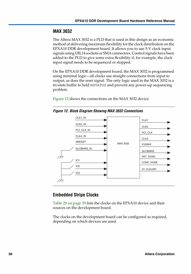
EPXA10 DDR Development Board Hardware Reference Manual
MAX 3032
The Altera MAX 3032 is a PLD that is used in this design as an economic method of delivering maximum flexibility for the clock distribution on the EPXA10 DDR development board It allows you to use 5-V clock input signals using DIL14 sockets or SMA connectors Control signals have been added to the PLD to give some extra flexibility if for example the clock input signal needs to be sequenced or stopped
On the EPXA10 DDR development board the MAX 3032 is programmed using minimal logicmdashall clocks use straight connections from input to output as does the reset signal The only logic used in the MAX 3032 is a tri-state buffer to held NSTATUS and prevent any power-up sequencing problem
Figure 12 shows the connections on the MAX 3032 device
Figure 12 Block Diagram Showing MAX 3032 Connections
Embedded Stripe Clocks
Table 29 on page 39 lists the clocks on the EPXA10 device and their sources on the development board
The clocks on the development board can be configured as required depending on which devices are used
MAX 3032
CLK1_IN
CLK2_IN
PCI_CLK_IN
CLK4_IN
NRESET
GLOBNRS_IN
IO1
IO3
IO2
CLK1
CLK2
PCI_CLK
CLK4
GLOBNRS
IO_CLKUSR
IO2MAX
INIT_DONE
CONF_DONE
38 Altera Corporation
EPXA10 DDR Development Board Hardware Reference Manual
Table 29 EPXA10 DDR development Board Clock Sources
EPXA10 Pin Name
EPXA10 Pin Number
Board Connection
Description Test Point
CLK_REF A28 STRIPE_CLK 50-MHz main clock provided to the synchronous memory and embedded processor Dedicated input
TP_CLK_REF
CLK1 N30 CLK1_INMAX303225JP3
12-MHz clock input TP_CLK1
CLK2 Y3 CLK2_INMAX303228JP8
25-MHz clock input TP_CLK2
CLK3 W30 JP9PCI_CLK_IN
32-MHz clock input TP_CLK3
CLK4 P3 CLK4_INMAX303222
48-MHz clock input TP_CLK4
IOCLK1A V30 NCLK1 Clock input in LVDS mode TP_NCLK1
IOCLK2A R3 NCLK2 Clock input in LVDS mode TP_NCLK2
IOCLK3A Y30 NCLK3 Clock input in LVDS mode TP_NCLK3
IOCLK4A N3 NCLK4 Clock input in LVDS mode TP_NCLK4
IOCLKFBIN1A AM28 NCLK1_FB Dedicated pin that allows external feedback to the PLL in LVDS mode
TP_NCLK1_FB
IOCLKFBIN2A J3 NCLK2_FB Dedicated pin that allows external feedback to the PLL in LVDS mode
TP_NCLK2_FB
IOLOCKOUT0 AC30 U1683 Status of ClockLock PLL1
IOLOCKOUT1 AK4 U168 Status of ClockLock PLL2
IOLOCKOUT2 H30 U1685 Status of ClockLock PLL3
IOLOCKOUT3 AK5 U163 Status of ClockLock PLL4
PLLENABL P30 U1683 Dedicated pin used for PLL circuitry
CLKOUT0 AM29 CLK1_OUT Dedicated pin that allows the PLL output to be driven off-chip
TP_CLK1_OUT
CLKOUT1 AH3 CLK2_OUT Dedicated pin that allows the PLL output to be driven off-chip
TP_CLK2_OUT
CLKFBIN0 AL28 CLK1_FBp Dedicated pin that allows external feedback to the PLL
TP_CLK1_FBp
CLKFBIN1 K3 CLK2_FBp Dedicated pin that allows external feedback to the PLL
TP_CLK2_FBp
Altera Corporation 39
EPXA10 DDR Development Board Hardware Reference Manual
Jumper Configuration for the Clock Input
Jumpers JP1 to JP10 are used to select different clock inputs
JP1 JP2 and JP4 to JP6 enable and disable the clocks (X1 X2 and X4 to X6 respectively)
JP3 is used to set CLK1 to oscillator 0 (position 1-2) or to the Ethernet clock TX_CLK (position 2-3)
JP7 enables and disables the Ethernet clock JP8 is used to set CLK2 to oscillator 1 (position 1-2) or to the Ethernet
clock RX_CLK (position 2-3) JP9 and JP10 can be used to connect CLK3 to lvdstxinclk1p and
NCLK3 to lvdstxclk1n respectively
During development if you need to run any of the clocks at a slower or faster rate you can do so using either the external clock input or a variable oscillator
Sources for the EPXA10 Clocks
There are three options for providing a source for the EPXA10 stripe clocks
External clock generator Main clock An alternative crystal oscillator
Using an External Clock Generator
To select the external clock generator for a clock input set the appropriate jumper to position 1-2 to disable the main clock
Using the Main Clock
To use the main clock for a clock input set the appropriate jumper to position 2-3 to enable the crystal oscillator
Using a Variable Oscillator
To use a variable oscillator as a clock input follow the steps below
1 Plug in the DIL14 crystal oscillator package to the appropriate socket
2 Disable the relevant main clock by connecting pins 1 and 2 of the appropriate jumper (see Table 26 on page 34)
40 Altera Corporation
EPXA10 DDR Development Board Hardware Reference Manual
3 Provide a 5-V power supply on the board either by connecting the ATX power supply or by connecting an alternative 5-V input to JP11
1 The clock buffer and the MAX 3032 are 5-V compatible they convert 5-V input from the crystal oscillator to the 33 V required for the clocksrsquo inputs
Device Configuration
There are three methods of configuring and programming the EPXA10 device
Booting from flash memory Configuring the device from the EPC16 Using the Quartusreg II software to configure the device using the
JTAG interface
1 On the EPXA10 device the settings of BOOT_FLASH MSEL0 and MSEL1 determine the configuration mode and method See Figure 10 on page 33 for their location on the EPXA10 DDR development board
See ldquoJTAG Interfacesrdquo on page 45 for more details about using a JTAG interface
Booting from Flash Memory
The Altera flash memory programmer (exc_flash_programmerexe) is a utility that allows you to program flash memory on the EBI using the JTAG interface and the ByteBlasterMV or MasterBlaster download cable
After reset the processor boots up and executes the bootloader from flash memory The bootloader configures the stripe loads the user software into memory configures the FPGA side of the EPXA10 and then begins to execute the user code
Table 30 summarizes the board jumper requirements for booting from flash memory
f For further details about booting the device from flash memory refer to the Excalibur Devices Hardware Reference Manual
Table 30 Jumper Settings for Booting from Flash Memory
BOOT_FLASH MSEL0 MSEL1 Mode
1 0 0 Boot from 16-bit flash
Altera Corporation 41
EPXA10 DDR Development Board Hardware Reference Manual
Configuring Using the EPC16
The Quartus II software can generate a programmer object file (pof) containing both hardware and software for downloading into the EPC16 device on the EPXA10 DDR development board For more details see ldquoEPC16 Configuration Devicerdquo on page 44
1 The EPC16 device can be programmed with the Quartus II software version 11 or higher using either the MasterBlaster or ByteBlasterMV download cables
Table 31 summarizes the jumper requirements for booting your system from an EPC16
When power is applied to the development board the EPC16 configuration device loads configuration data into the EPXA10 device if it has been programmed If you change the configuration devicersquos programming information you must turn the board off and on before new information can be loaded into the EPXA10 device
The EPC16 device can be programmed through the JTAG interface see ldquoEPC16 Configuration Devicerdquo on page 44
To configure the device using the EPC16 device start the Quartus II software and specify the EPC16 as an output option to create the required pof files If the EPC16 is not specified the Quartus II software generates a single file to program the EPXA10 device directly
When configuring an Excalibur device using the EPC16 configuration device some simple logic must be placed in the system to allow both the Excalibur and EPC16 devices to fully come out of reset before any configuration begins
During a configuration the EPC16 uses the signals OE (connected to nSTATUS on the Excalibur device) and nCS (connected to CONF_DONE on the Excalibur device) to determine what action it should take
Table 31 Jumper Settings for Booting from a Serial Device
BOOT_FLASH MSEL0 MSEL1 Mode
0 0 0 Serial
42 Altera Corporation
EPXA10 DDR Development Board Hardware Reference Manual
In its long power-on-reset (POR) mode the EPC16 begins sampling CONF_DONE and OE approximately 100 ms after power-up If the Excalibur device is still in POR after this 100 ms the signals from the Excalibur device that control the state of the EPC16 could be in an unknown state when the EPC16 begins sampling them which results in indeterminate behavior Therefore you must provide logic to hold these signals low until the Excalibur devicersquos nRESET signal is deasserted By holding nSTATUS and OE low the reset of the EPC16 can be extended until the Excalibur device has also come out of POR By holding CONF_DONE and nCS low the EPC16 does not erroneously sample it as being high which falsely indicates that the Excalibur device has already been configured Because both signals are open-drain they can safely be driven low by external logic without causing contention Once nRESET goes high the Excalibur device is ready and the signals can be tri-stated by the external logic to operate normally As opposed to nPOR nRESET deasserts some time after the Excalibur device comes out of POR For this reason use the nRESET signal not NPOR to control the tri-stating of nSTATUS and CONF_DONE to provide a margin of safety Figure 13 shows the circuit that accomplishes the reset dependency requirements
Figure 13 Reset Dependency Circuit
Configuring Using JTAG
The Quartus II software can generate an SRAM object file (sof) containing both hardware and software
The Quartus II programmer uses the sof file to configure the EPXA10 device via JTAG using either the MasterBlaster or ByteBlasterMV download cables For more details see ldquoMasterBlasterByteBlasterMV Communications Cablerdquo on page 44
For further details of how to create a sof file and configure the EPXA10 device via JTAG consult the Quartus II Help
Table 32 summarizes the jumper requirements for booting your system from an EPC16
CONF_DONE and nCS
nSTATUS and OE
nRESET
Altera Corporation 43
EPXA10 DDR Development Board Hardware Reference Manual
Configuration Schemes
Table 33 lists the serial configuration schemes that are available for the EPXA10 device
EPC16 Configuration Device
The EPC16 is part of the on-board JTAG chain that allows in-system programming The device is an EPC16 88-pin Ultra FineLine BGA it contains reprogrammable flash memory to use for serial device configuration For more details about configuring these devices refer to the data sheet Configuration Devices for ACEX APEX FLEX amp Mercury Devices
f For signal details of the EPC16 device refer to the EPC16 pin-out table
MasterBlasterByteBlasterMV Communications Cable
The ByteBlasterMV and MasterBlaster cables have a 10-pin header for use with the development board The cable allows you to download hardware and software configuration data directly to the EPXA10 device or to the EPC16 configuration device The development board supports only JTAG download mode not passive serial download mode The MasterBlaster and ByteBlasterMV cables also support in-circuit hardware debugging with the SignalTapreg embedded logic analyzer
1 The MasterBlaster cable can also be used in conjunction with the ARM debugger to debug your software using JTAG
Debugging Features
On the EPXA10 DDR development board a variety of debugging tools both Altera and third-party products can be used in conjunction with the JTAG interfaces to debug systems under development
Table 32 Jumper Settings for Configuring Using JTAG
BOOT_FLASH MSEL0 MSEL1 Mode
1 0 0 Serial
Table 33 Supported Serial Configuration Schemes
Configuration Scheme Data Source
Configuration device EPC16 configuration device
JTAG MasterBlasterByteBlasterMV download cable
44 Altera Corporation
EPXA10 DDR Development Board Hardware Reference Manual
Third-Party Debugging Tools
Third-party debugging tools such as Lauterbach and the GNUPro XRAY debugger can be used with the EPXA10 DDR development board For latest details of which tools are available access the Altera website at httpwwwAlteracom
JTAG Interfaces
There are three JTAG interfaces on the EPXA10 DDR development board
The MB_BLASTER connector is used to connect an Altera ByteBlaster or MasterBlaster download cable
The MULTI_ICE connector is used to connect a Multi-ICE cable or any other compatible cable
The TRACE_PORT connector is used to connect a trace capture unit or logic analyzer
The MB_BLASTER connector can be used with both the flash programmer and the Quartus programmer using the ByteBlasterMV and MasterBlaster cables and can be used to program the EPC16 The MasterBlaster and ByteBlasterMV cables also support in-circuit hardware debugging on the MB_BLASTER connector using the SignalTapreg embedded logic analyzer The JSELECT setting does not affect these functions
Using JSELECT
The JSELECT jumper determines whether a JTAG debugger can be connected to the MB_BLASTER connector the MULTI_ICE connector or the TRACE_PORT connector shows the JSELECT settings required
Table 34 Using JSELECT to Select a Debugging Connector
Debugger JSELECT Value
Altera-RDI via a ByteBlasterMV or MasterBlaster cable lsquo1rsquo
Multi-ICE or a compatible device on the Multi-ICE connector lsquo0rsquo
Trace port connector or a compatible device on the trace port connector
lsquo0rsquo
Altera Corporation 45
EPXA10 DDR Development Board Hardware Reference Manual
1 Damage can result if you simultaneously connect a device that drives the JTAG pins on the trace port connector and another device on the Multi-ICE connector
You can simultaneously connect one device to the MB_BLASTER connector and another to one of the other two connectors or you can connect devices to the trace port and Multi_ICE connectors at the same time providing that the device on the trace port connector does not drive the JTAG pins on that connector
Using MasterBlasterByteBlasterMV Cable to Program the EPC16 Device
The EPC16 device can be programmed using the Quartus II software version 11 or higher using either the MasterBlaster or ByteBlasterMV download cable
Figure 14 on page 47 shows how the MasterBlaster ByteBlasterMV and Multi-ICE cables are connected
46 Altera Corporation
EPXA10 DDR Development Board Hardware Reference Manual
Figure 14 Connecting the MasterBlaster ByteBlasterMV or Multi-ICE Cables
Power Supply
The EPXA10 DDR development board can be powered by either a laboratory bench power supply or a commercially-available PC-style power supply (ATX) The bench supply provides 33-V the ATX supply provides voltage levels of plusmn12 V plusmn5 V and +33 V The development board derives VTT (125-V) VREF (125-V) +25-V and +18-V supplies from the input power supply If there are no devices attached to the PCI connectors only the 33-V supply input is necessary but to use devices on the PCI connectors you need an ATX power supply to provide the different voltages
1 Ensure that the voltage setting on the ATX power supply is set to the appropriate voltage based on the AC power outlet supply
Figure 15 on page 48 shows the location of the power supply inputs for the EPXA10 DDR development board
Multi_ICE
JSELECT
MB Blaster
EPXA10Device
Development Board
10 24
135
68
79102 4
1 3
20
5
6 8 12 14 16 18
7 9 11 13 15 17 19
123456789
10
TCKGNDTDOVCCTMSVIOTCKNCTDIGND
123456789
1011121314151617181920
VCCVCCPROC_NTRSTGNDPROC_TDIGNDPROC_TMSGNDPROC_TCKGNDGNDGNDPROC_TDOGNDNSRSTGNDNCGNDNCGND
Altera Corporation 47
EPXA10 DDR Development Board Hardware Reference Manual
Figure 15 EPXA10 Power Supply Inputs
1 See Figure 1 on page 11 to see the development board layout in greater detail
A status LED is provided for each power supply source see Table 19 on page 24
5 V
33 V
GND
GNDNC
20
111
10
2019181716151413121110
987654321
5 V5 V-5 VGNDGNDGNDmain switchGND-12 V33 V12 VNCPWR_OKGND5 VGND5 VGND33 V33 V
48 Altera Corporation
EPXA10 DDR Development Board Hardware Reference Manual
1 The total current that can be drawn depends on the daughter card power supply as follows 1 A for 33 V 5 V or 12 V and 100 mA for ndash12 V This can be drawn from a single pin but designers should use as many of pins available on the header as possible to ease the power distribution on the daughter card
Tables 35 through 40 list the estimated power requirements for the development board
Table 35 plusmn120-V Supply Requirements
Module mA (12 V) mA (ndash12 V)
PCIs 500 100
Table 36 50-V Supply Requirements
Module mA (5 V)
PCI Depends on system
CLK_REF Alternative crystal oscillator
CLK1 5
CLK2 5
CLK3 5
CLK4 5
ATX PSU 1000 (to provide adequate regulation)
Table 37 33-V Supply Requirements
Module mA (33 V)
EPXA10 IO Depends on application
Flash memory 300
PCIs 76A (system-dependent)
UARTs 50
Ethernet -
LEDs 20 times 22
EPC16 50
Crystal oscillator 15 times 5
Power-on reset 10
Clock buffers 32 times 2
Altera Corporation 49
EPXA10 DDR Development Board Hardware Reference Manual
Table 38 25-V Supply Requirements
Module mA (25 V)
DDR SDRAM 500 mA
Table 39 18-V Supply Requirements
Module mA (18 V)
EPXA10 device core Depends on application
Table 40 125-V Supply Requirements
Module mA (125 V)
VTT 1500
VREF 25
50 Altera Corporation
EPXA10 DDR Development Board Hardware Reference Manual
Test Points Table 41 on page 51 lists the test points on the EPXA10 DDR development board
Table 41 EPXA10 DDR development Board Test Points
Test Point Connected To Test Point Connected To
GND1 GND TP_NCLK1_FB NCLK1_FB
GND2 GND TP_NCLK2_FB NCLK2_FB
GND3 GND TP_CS0_N CS0_N
GND4 GND TP_CS1_N CS1_N
GND5 GND TP_CS2_N CS2_N
GND6 GND TP_CS3_N CS3_N
GND7 GND TP_EBI_CLK EBI_CLK
TP_CLK_REF CLK_REF TP_OE_N OE_N
TP_CLK1 CLK1 TP_WE_N WE_N
TP_CLK2 CLK2 TP_TCK TCK
TP_CLK3 CLK3 TP_TDI TDI1
TP_CLK4 CLK4 TP_TDO TDO1
TP_CLK1_FBP CLK1_FBP TP_TMS TMS1
TP_CLK1_OUT CLK1_OUT ndash12V Test points for input power supplyTP_CLK2_FBP CLK2_FBP ndash5V
TP_CLK2_OUT CLK2_OUT 18V
TP_NCLK1 NCLK1 12V
TP_NCLK2 NCLK2 25V
TP_NCLK3 NCLK3 33V
TP_NCLK4 NCLK4 5V
U34 ATX POWER_OK
Altera Corporation 51
EPXA10 DDR Development Board Hardware Reference Manual
Signals Tables 42 through 46 document the signals for the following peripherals
UART PCI card Trace port Configurationdebugging interfaces
UART
Figure 16 shows the UART DB9 male connector used on the development board
Figure 16 DTE UART DB9 Male Connector
Table 42 lists the UART DB9 signals
Note(1) The EPXA10 DDR development board has two DB9 male connectors
See Table 53 on page 64 for UART pin-out information
1 2 3 4 56 7 8 9
Table 42 DTE UART DB9 Male Connector Signals Note (1)
Pin Signal Description
1 DCD Data carrier detect
2 RXD Receive data
3 TXD Transmit data
4 DTR Data terminal ready
5 GND Signal ground
6 DSR Data set ready
7 RTS Request to send
8 CTS Clear to send
9 RI Ring indicator
52 Altera Corporation
EPXA10 DDR Development Board Hardware Reference Manual
PCI
Table 43 lists the PCI connector signals used on the development board
See Table 52 on page 63 for pin-out information for the PCI connectors
Table 43 PCI Card 33-V-Only Connector
Pin Signal Pin Signal Pin Signal Pin SIgnal
A1 TRST A2 +12 V B1 ndash12 V B2 TCK
A3 TMS A4 TDI B3 GND B4 TDO
A5 +5 V A6 INTA B5 +5 V B6 +5 V
A7 INTC A8 +5 V B7 INTB B8 INTD
A9 RESERVED A10 V IO B9 PRSNT1 B10 RESERVED
A11 RESERVED A12 RESERVED B11 PRSNT2 B12 RESERVED
A13 RESERVED A14 33 V AUX B13 RESERVED B14 RESERVED
A15 RST A16 V IO B15 GND B16 PCI_CLK
A17 V IO A18 GNT1 B17 GND B18 REQ1
A19 GND A20 AD [30] B19 V IO B20 AD [31]
A21 + 33 V A22 AD [28] B21 AD [29] B22 GND
A23 AD [26] A24 GND B23 AD [27] B24 AD [25]
A25 AD[24] A26 IDSEL B25 VCC B26 CBE3
A27 + 33 V A28 AD[22] B27 AD[23] B28 GND
A29 AD[20] A30 GND B29 AD[21] B30 AD[19]
A31 AD[18] A32 AD[16] B31 VCC B32 AD[17]
A33 + 33 V A34 FRAME B33 CBE2 B34 GND
A35 GND A36 TRDY B35 IRDY B36 + 33 V
A37 GND A38 STOP B37 DEVSEL B38 GND
A39 + 33 V A40 RESERVED B39 LOCK B40 PERR
A41 RESERVED A42 GND B41 + 33 V B42 SERR
A43 PAR A44 AD[15] B43 + 33 V B44 CBE1
A45 + 33 V A46 AD[13] B45 AD[14] B46 GND
A47 AD[11] A48 GND B47 AD[12] B48 AD[10]
A49 AD[9] A50 GND B49 M66EN B50 GND
A51 GND A52 CBE0 B51 GND B52 AD[8]
A53 + 33 V A54 AD[6] B53 AD[7] B54 + 33 V
A55 AD[4] A56 GND B55 AD[5] B56 AD[3]
A57 AD[2] A58 AD[0] B57 GND B58 AD[1]
A59 V IO A60 REQ64 B59 + 33 V B60 ACK64
A61 + 5 V A62 + 5 V B61 + 5 V B62 + 5 V
Altera Corporation 53
EPXA10 DDR Development Board Hardware Reference Manual
Trace Port
Table 44 lists the ETM9 trace port signals
See Table 57 on page 66 for pin-out information for the ETM9 trace port
Table 44 Trace Port Signals
Pin Signal Description Pin Signal Description
1 NC No connection 2 NC No connection
3 NC No connection 4 NC No connection
5 GND Ground 6 TRACECLK Clock output for the trace port
7 DBGRQ Not used 8 DBGACK Output (not used)
9 nSRST System reset detector 10 EXTTRIG Output (not used)
11 TDO Test data input 12 VTRef Reference voltage input
13 RTCK Input (not used) 14 VSupply Power input for the debug equipment
15 TCK Test clock output 16 TRACEPKT7 Dataaddress information output on pipeline status17 TMS Test mode select output 18 TRACEPKT6
19 TDI Test data output 20 TRACEPKT5
21 nTRST Reset inputoutput 22 TRACEPKT4
23 TRACEPKT15 Dataaddress information output on pipeline status
24 TRACEPKT3
25 TRACEPKT14 26 TRACEPKT2
27 TRACEPKT13 28 TRACEPKT1
29 TRACEPKT12 30 TRACEPKT0
31 TRACEPKT11 32 TRACESYNC
33 TRACEPKT10 34 PIPESTAT2 Processor pipeline status
35 TRACEPKT9 36 PIPESTAT1
37 TRACEPKT8 38 PIPESTAT0
39 GND Ground 40 GND Ground
41 GND Ground 42 GND Ground
43 GND Ground
54 Altera Corporation
EPXA10 DDR Development Board Hardware Reference Manual
ConfigurationDebugging Interfaces
On the development board there are interfaces for a MasterBlaster or ByteBlasterMV cable and a Multi-ICE connector Table 45 lists the signals on the MasterBlasterByteBlasterMV interface
See Table 47 on page 58 for pin-out information for the development board configuration and debugging interfaces
Table 45 MasterBlasterByteBlasterMV Female Interface
Pin JTAG Mode
Signal Description
1 TCK Clock signal
2 GND Signal ground
3 TDO Data from device
4 Vcc Power supply
5 TMS JTAG state machine control
6 Vio Reference voltage for MasterBlasterByteBlasterMV output driver
7 TCK Clock signal
8 ndash No connection
9 TDI Data to device
10 GND Signal ground
Altera Corporation 55
EPXA10 DDR Development Board Hardware Reference Manual
Table 46 lists the signals on the Multi-ICE interface
See Table 47 on page 58 for pin-out information for the development board configuration and debugging interfaces
f For signal details of the EPC16 device refer to the EPC16 pin-out table
See Table 57 on page 66 for pin-out information for the trace port
Table 46 Multi-ICE Connector
Pin Signal Description Direction
1 Vcc Power supply NA
2 Vcc Power supply NA
3 PROC_NTRTS Processor reset O
4 GND Ground NA
5 PROC_TDI Processor test data input I
6 GND Ground NA
7 PROC_TMS Processor test mode select I
8 GND Ground NA
9 PROC_TCK Processor test clock input I
10 GND Ground NA
11 GND Ground NA
12 GND Ground NA
13 PROC_TDO Processor test data output O
14 GND Ground NA
15 NSRST Warm reset IO
16 GND Ground NA
17 NC No connection NA
18 GND Ground NA
19 NA No connection NA
20 GND Ground NA
56 Altera Corporation
EPXA10 DDR Development Board Hardware Reference Manual
Pin-Outs The main component of the development board is the EPXA10F1020C1 device The pins on the EPXA10 device are assigned to functions on the board When generating IP cores for the EPXA10 device the pins must be used as defined to avoid damaging the device and any unused pins must be tri-stated using the Quartus II software The following sections list the interfaces and dedicated pins on the board Any pins not used for a design should be left in the high-impedance (input) state to avoid contention
This section details the EPXA10 device pins that are assigned to the following purposes
Configuration DDR SDRAM EBI UARTs 1 and 2 Ethernet User LEDs push buttons and dip-switches Fast IO pins IDC 10-pin header Trace port Test points
Pin assignments are grouped into tables for control pins bank address pins and data bus pins where appropriate The tables also detail signals passing across a connection The remaining IO pins on the EPXA10 device are listed at the end of this section
Configuration
The EPXA10 device pins listed in Table 47 on page 58 are used exclusively for configuring the device Refer to ldquoDevice Configurationrdquo on page 41 for more information about EPXA10 configuration
Altera Corporation 57
EPXA10 DDR Development Board Hardware Reference Manual
Table 47 EPXA10 Device Configuration Pins
Signal Name EPXA10 Device Pin Description
MSEL0 J30 Configuration mode select (tied to GND)
MSEL1 K30 Configuration mode select (tied to GND)
NSTATUS AM14 OE for EPC16
NCONFIG R30 n_INIT_CONF for EPC16
DCLK W3 Data clock for EPC16
CONF_DONE AM13 Configuration complete indicator
INIT_DONE D14 Initialization complete indicator
nCE AC3 Not connected
nCEO D13
DATA0 V3 Serial input for EPC16 configuration data
DATA1 D10 Serial input for EPC16 configuration data available for user IO after configurationDATA2 A9
DATA3 B9
DATA4 C9
DATA5 D9
DATA6 A4
DATA7 B4
TDI AD3 JTAG data input
TDO E11 JTAG data output (to next device in the chain
TCK AM19 JTAG clock
TMS AM20 JTAG mode select
TRST C13 JTAG reset (pulled high)
PROC_TDI H27 JTAG data input
PROC_TDO H26 JTAG data output (to next device in the chain
PROC_TCK D30 JTAG clock
PROC_TMS E29 JTAG mode select
PROC_TRST E30 JTAG reset (pulled high)
DEV_CLRn H3 Global reset for the device
DEV_OE AE3 Device output enable
nWS C4 Write strobe
nRS D4 Read strobe
nCS D3 Signal providing handshaking between devices
CS E3 Chip select
RDYnBSY E14 Readybusy
CLKUSR A13 Clock signal
58 Altera Corporation
EPXA10 DDR Development Board Hardware Reference Manual
DDR SDRAM Interface
There are four DDR chips (256-Mbit times 8) on the EPXA10 DDR development board selectable using one chip-select SD_CS0_N The development board DDR interface can run at up to 266 MHz
f For more details on how to use the DDR SDRAM ref to AN141 Using the SDRAM Controller
Table 48 lists the pin-outs for the DDR SDRAM control signals
Table 49 on page 60 lists the DDR SDRAM data bank and address bus pin-outs
Table 48 DDR SDRAM Control Signal Pin-Outs
Signal Name EPXA10 Device Pin Description
SD_RAS_N F17 Row address strobe
SD_CAS_N F18 Column address strobe
SD_WE_N G18 Write enable
SD_CS0_N G14 Chip select
SD_CS1_N F16 Chip select
SD_CLKE F14 Clock enable
SD_CLK F15 SDRAM clock
SD_CLK_N G13 SDRAM clock - inverted
SD_DQM(0) H14 Data byte mask
SD_DQM(1) L14 Data byte mask
SD_DQM(2) K9 Data byte mask
SD_DQM(3) H9 Data byte mask
SD_DQS(0) J14 DQS signal
SD_DQS(1) K14 DQS signal
SD_DQS(2) K10 DQS signal
SD_DQS(3) H10 DQS signal
Altera Corporation 59
EPXA10 DDR Development Board Hardware Reference Manual
Table 49 DDR SDRAM Data Bank amp Address Bus Pin-Outs
Signal Name EPXA10 Device Pin
Signal Name EPXA10 Device Pin
Signal Name EPXA10 Device Pin
SD_DQ0 H18 SD_DQ1 H17 SD_DQ2 H16
SD_DQ3 J18 SD_DQ4 J17 SD_DQ5 H15
SD_DQ6 J16 SD_DQ7 J15 SD_DQ8 K18
SD_DQ9 K17 SD_DQ10 L18 SD_DQ11 K16
SD_DQ12 L17 SD_DQ13 L16 SD_DQ14 K15
SD_DQ15 L15 SD_DQ16 L13 SD_DQ17 K13
SD_DQ18 L12 SD_DQ19 K12 SD_DQ20 L11
SD_DQ21 K11 SD_DQ22 L10 SD_DQ23 L9
SD_DQ24 H13 SD_DQ25 H12 SD_DQ26 J13
SD_DQ27 J12 SD_DQ28 J11 SD_DQ29 J10
SD_DQ30 J9 SD_DQ31 H11 SD_ADD0 G12
SD_ADD1 F13 SD_ADD2 G11 SD_ADD3 F12
SD_ADD4 F11 SD_ADD5 G10 SD_ADD6 F10
SD_ADD7 F9 SD_ADD8 G9 SD_ADD9 F8
SD_ADD10 G8 SD_ADD11 F7 SD_ADD12 F6
SD_ADD13 G7 SD_ADD14 G6
60 Altera Corporation
EPXA10 DDR Development Board Hardware Reference Manual
EBI
Table 50 lists the EPXA10 pin-outs for the EBI control signals
Table 50 EBI Control Signal Pin-Outs
Signal Name EPXA10 Device Pin Description
EBI_BE0 F27 Byte enable
EBI_BE1 E27 Byte enable
EBI_OE F26 Output enable
EBI_WE E26 Write enable
EBI_CS0 A25 Chip select
EBI_CS1 B25 Chip select
EBI_CS2 C25 Chip select
EBI_CS3 D25 Chip select
EBI_CLK E25 EBI clock
EBI_ACK F25 EBI acknowledge
INT_EXTPIN_N G25 Interrupt generated by push-button SW4
Altera Corporation 61
EPXA10 DDR Development Board Hardware Reference Manual
Table 51 lists the EBI data bank and address bus pin-outs
Table 51 EBI Data Bank and Address Bus Pin-Outs
Signal Name EPXA10 Device Pin
Signal Name EPXA10 Device Pin
EBI_DQ0 J21 EBI_DQ1 H21
EBI_DQ2 E20 EBI_DQ3 F20
EBI_DQ4 E19 EBI_DQ5 L20
EBI_DQ6 K20 EBI_DQ7 J20
EBI_DQ8 H20 EBI_DQ9 G20
EBI_DQ10 F19 EBI_DQ11 G19
EBI_DQ12 L19 EBI_DQ13 K19
EBI_DQ14 J19 EBI_DQ15 H19
EBI_A0 H25 EBI_A1 D24
EBI_A2 E24 EBI_A3 F24
EBI_A4 G24 EBI_A5 J24
EBI_A6 H24 EBI_A7 E23
EBI_A8 F23 EBI_A9 G23
EBI_A10 K23 EBI_A11 J23
EBI_A12 H23 EBI_A13 E22
EBI_A14 F22 EBI_A15 E21
EBI_A16 L22 EBI_A17 K22
EBI_A18 J22 EBI_A19 H22
EBI_A20 G22 EBI_A21 F21
EBI_A22 G21 EBI_A23 L21
EBI_A24 K21
62 Altera Corporation
EPXA10 DDR Development Board Hardware Reference Manual
PCI
Table 52 lists the pins used for the PCI cards
Table 52 PCI Pin-Outs
FPGA UART Embedded Stripe UART
EPXA10 Device Pin
Device Signal (Board Signal)
EPXA10 Device Pin
Device Signal (Board Signal)
AF21 CBE0 AF22 A5 (PCI_BUS5)
AE19 CBE1 AG22 A6 (PCI_BUS6)
AF19 CBE2 AH22 A7 (PCI_BUS7)
AJ18 CBE3 AD21 A8 (PCI_BUS8)
AG19 DEVSEL AE21 A9 (PCI_BUS9)
AH19 FRAME AG21 A10 (PCI_BUS10)
AB20 GNT1 AH21 A11 (PCI_BUS11)
AC20 GNT2 AD20 A12 (PCI_BUS12)
AB22 INTA AE20 A13 (PCI_BUS13)
AG23 INTB AF20 A14 (PCI_BUS14)
AC22 INTC AH20 A15 (PCI_BUS15)
AF23 INTD AJ19 A16 (PCI_BUS16)
AK20 PAR AK19 A17 (PCI_BUS17)
AB18 PCI_RST AL19 A18 (PCI_BUS18)
AL18 PERR AD18 A19 (PCI_BUS19)
AB21 PRSNT1 AE18 A20 (PCI_BUS20)
AC22 PRSNT2 AF18 A21 (PCI_BUS21)
AD19 REQ1 AG18 A22 (PCI_BUS22)
AC19 REQ2 AH18 A23 (PCI_BUS23)
AB19 SERR AK18 A24 (PCI_BUS24)
AB17 STOP AC17 A25 (PCI_BUS25)
AC18 TRDY AD17 A26 (PCI_BUS26)
AK23 A0 (PCI_BUS0) AE17 A27 (PCI_BUS27)
AL23 A1 (PCI_BUS1) AF17 A28 (PCI_BUS28)
AM23 A2 (PCI_BUS2) AG17 A29 (PCI_BUS29)
AD22 A3 (PCI_BUS3) AH17 A30 (PCI_BUS30)
AE22 A4 (PCI_BUS4) AJ17 A31 (PCI_BUS31)
Altera Corporation 63
EPXA10 DDR Development Board Hardware Reference Manual
UART1 amp UART2
Table 53 lists the pins used for UARTs 1 and 2
Ethernet
Table 53 lists the pins used for the Ethernet interface
Table 53 Extension Header UARTs 1 amp 2 IO Pin-Outs
FPGA UART Embedded Stripe UART
EPXA10 Device Pin
Device Signal Expansion Board Connector
EPXA10 Device Pin
Device Signal Expansion Board Connector
J27 UART2_DTR_N U16171 G28 UART1_CTS_N NC
J29 UART2_TXD U16174 D29 UART1_RXD NC
K29 UART2_RXD_N U16177 E28 UART1_RI_N NC
K27 UART2_DSR_N U16179 C28 UART1_RTS_N NC
J28 UART2_RTS_N U16173 F28 UART1_DSR_N NC
J26 UART2_RI_N U16175 G27 UART1_DCD_N NC
K28 UART2_DCD_N U16178 D28 UART1_TXD NC
K26 UART2_CTS_N U16181 G26 UART1_DTR_N NC
Table 54 Extension Header Ethernet Pin-Outs
EPXA10 Device Pin
Device Signal Expansion Board Connector
EPXA10 Device Pin
Device Signal Expansion Board Connector
R23 RXD1 U16155 R24 TXD3 U16153
R25 TXD0 U16149 M19 MDC U16145
M20 RST_N U16146 M21 TX_ER U16161
M22 TX_EN U16162 M23 RXD2 U16157
N19 CRS U16166 N20 COL U16163
N21 RX_DV U16167 N22 MDIO U16169
N23 RXD0 U16154 P20 INTR U16147
P21 RX_ER U16165 P22 RX_D3 U16158
N25 TXD1 U16150 P25 TXD2 U16151
64 Altera Corporation
EPXA10 DDR Development Board Hardware Reference Manual
Fast IO Pins
Table 55 lists the pins used for the EPXA10 fast IO pins
User LEDs Switches amp Push Button Switches
Table 56 lists the pins used for the user-defined LEDs push-button switches and dip-switches
Table 55 EPXA10 Fast IO Pins
EPXA10 Pin Name
Description EPXA10 Device Pin
Expansion Board Connector
Board Reference
FAST0 Dedicated fast IO pins E13 U16133 FAST0
FAST1 Dedicated fast IO pins E12 U16134 FAST1
FAST2 Dedicated fast IO pins AM18 U16135 FAST2
FAST3 Connected to PCI to provide IRDY AM15 IRDY
Table 56 Expansion Header LED Switch and Push Button IO Pin-Outs
EPXA10 Device Pin
Device Signal Expansion Board Connector
EPXA10 Device Pin
Device Signal Board Connector
V6 USER_LED0 U181 U5 USER_LED1 U183
V5 USER_LED2 U184 U6 USER_LED3 U185
V7 USER_LED4 U187 V8 USER_LED5 U188
U7 USER_LED6 U189 T6 USER_LED7 U1811
U8 USER_SW0 U1812 T5 USER_SW1 U1813
V4 USER_SW2 U1815 V10 USER_SW3 U1816
T7 USER_SW4 U1817 W12 USER_SW5 U1817
U9 USER_SW6 U1820 V11 USER_SW7 U1821
R6 USER-SW8 U1823 T8 USER_PB0 U1824
R5 USER_PB1 U1825 U4 USER_PB2 U1827
U10 USER_PB3 U1828
Altera Corporation 65
EPXA10 DDR Development Board Hardware Reference Manual
Trace Port
Table 57 lists the pins used on the trace port interface
IDC 10-Pin Header
Table 56 lists the pins used for the 10-pin IDC header
Table 57 Trace Port Pin-Out
EPXA10 Device Pin
Device Signal EPXA10 Device Pin
Device Signal
H6 TRACEPKT15 N7 TRACEPKT4
J6 TRACEPKT14 H8 TRACEPKT3
K6 TRACEPKT13 J8 TRACEPKT2
L6 TRACEPKT12 K8 TRACEPKT1
M6 TRACEPKT11 L8 TRACEPKT0
N6 TRACEPKT10 M8 TRACESYNC
H7 TRACEPKT9 M9 PIPESTAT2
J7 TRACEPKT8 N9 PIPESTAT1
K7 TRACEPKT7 N10 PIPESTAT0
L7 TRACEPKT6 N8 TRACECLK
M7 TRACEPKT5
Table 58 IDC Header Pin-Outs
EPXA10 Device Pin Header Pin Expansion Board Connector
L5 Header11 U1871
K4 Header12 U1872
J4 Header13 U1873
H4 Header14 U1875
K5 Header15 U1876
E4 Header16 U1877
J5 Header17 U1879
H5 Header18 U1880
GND Header19 na
GND Header110 na
66 Altera Corporation
EPXA10 DDR Development Board Hardware Reference Manual
Expansion Header
The pins on the expansion header cards connect to IO pins on the EPXA10 device to ground or to VCC supplies
IO Pin-Outs
Tables 59 to 62 list the pins on the EPXA10 DDR development board expansion header cards that connect to IO pins on the EPXA10 device Some of these pins can optionally be dedicated to the Ethernet UART user LEDs push-button switches and dip-switches
Table 59 Development Board Expansion Header U15 IO Pin-Outs (Part 1 of 2)
U151-50 Device U1551-100 Device U15101-150
Device U15151-200
Device
U151 AB24 U1551 AC23 U15101 GND U15151 Y5
U152 GND U1552 AD23 U15102 W4 U15152 Y8
U153 L24 U1553 AE23 U15103 W5 U15153 GND
U154 L26 U1554 GND U15104 AA6 U15154 Y7
U155 L27 U1555 AL20 U15105 GND U15155 Y4
U156 GND U1556 AJ20 U15106 W8 U15156 B24
U157 AJ29 U1557 AG20 U15107 Y6 U15157 GND
U158 AK29 U1558 GND U15108 W7 U15158 A24
U159 AH28 U1559 AJ30 U15109 GND U15159 D23
U1510 GND U1560 IOData7 U15110 W6 U15160 C23
U1511 AJ28 U1561 IOData6 U15111 AF5 U15161 GND
U1512 AK28 U1562 GND U15112 AE4 U15162 B23
U1513 AH27 U1563 IOData5 U15113 GND U15163 A23
U1514 GND U1564 IOData4 U15114 AD4 U15164 D20
U1515 AH26 U1565 IOData3 U15115 AC4 U15165 GND
U1516 AG26 U1566 GND U15116 AE5 U15166 C20
U1517 AF26 U1567 IOData2 U15117 GND U15167 B20
U1518 GND U1568 IOData1 U15118 AD8 U15168 A20
U1519 AM25(1) U1569 N26 U15119 AA12 U15169 GND
U1520 AL25 U1570 GND U15120 AC9 U15170 D19
U1521 AK25(1) U1571 N29 U15121 GND U15171 C19
U1522 GND U1572 IOCLKUSR U15122 AD5 U15172 B19
U1523 AJ25(1) U1573 IORDYNBSY U15123 AC5 U15173 GND
U1524 AH25 U1574 GND U15124 AD7 U15174 A19
U1525 AG25 U1575 NRS U15125 GND U15175 A18
Altera Corporation 67
EPXA10 DDR Development Board Hardware Reference Manual
U1526 GND U1576 IONWS U15126 AA11 U15176 B18
U1527 AF25 U1577 IONCS U15127 Y12 U15177 GND
U1528 AE25 U1578 GND U15128 AC8 U15178 D18
U1529 AD25 U1579 IOCS U15129 GND U15179 E18
U1530 GND U1580 M25 U15130 AB5 U15180 D17
U1531 AC25 U1580 M26 U15131 AB9 U15181 GND
U1532 AB25 U1581 P27 U15132 AA10 U15182 E17
U1533 AM24 U1582 GND U15133 GND U15183 D16
U1534 GND U1583 M28 U15134 Y11 U15184 E16
U1535 AL24 U1584 NC U15135 AD6 U15185 GND
U1536 AK24 U1585 NC U15136 AA5 U15186 D15
U1537 AJ24 U1586 GND U15137 GND U15187 B15
U1538 GND U1587 NCLK3 U15138 AC7 U15188 A15
U1539 AH24 U1588 GND U15139 AB8 U15189 GND
U1540 AC24 U1589 NCLK4 U15140 Y10 U15190 B14
U1541 AD24 U1590 GND U15141 GND U15191 A14
U1542 GND U1591 CLK2_OUT U15142 W11 U15192 E15
U1543 AE24 U1592 GND U15143 AA8 U15193 GND
U1544 AF24 U1593 NCLK2_FB U15144 AB7 U15194 C14
U1545 AG24 U1594 GND U15145 GND U15195 NCLK1_FB
U1546 GND U1595 CLK2_FBP U15146 AC6 U15196 GND
U1547 AJ23 U1596 GND U15147 W10 U15197 CLK1_FBP
U1548 AH23 U1597 NCLK2 U15148 AA7 U15198 GND
U1549 AB23 U1598 GND U15149 GND U15199 NCLK1
U1550 GND U1599 CLK1_OUT U15150 AB6 U15200 GND
Table 59 Development Board Expansion Header U15 IO Pin-Outs (Part 2 of 2)
U151-50 Device U1551-100 Device U15101-150
Device U15151-200
Device
68 Altera Corporation
EPXA10 DDR Development Board Hardware Reference Manual
Table 60 Development Board Expansion Header U16 IO Pin-Outs (Part 1 of 2)
U161-50 Device U1651-100
Device U16101-150
Device U16151-200
Device
U161 GND U1651 AD2 U16101 IOLVDSDSKW U16151 P25
U162 AE3 U1652 GND U16102 GND U16152 GND
U163 AK5 U1653 AE1 U16103 W32 U16153 R24
U164 GND U1654 AE2 U16104 W31 U16154 N23
U165 AM5 U1655 GND U16105 GND U16155 R23
U166 AL5 U1656 AH1 U16106 V31 U16156 GND
U167 GND U1657 AH2 U16107 V32 U16157 M23
U168 AK4 U1658 GND U16108 GND U16158 P22
U169 AJ3 U1659 AJ1 U16109 R32 U16159 NC
U1610 GND U1660 AJ2 U16110 R31 U16160 GND
U1611 AL4 U1661 GND U16111 GND U16161 M21
U1612 AM4 U1662 B29 U16112 P31 U16162 M22
U1613 GND U1663 A29 U16113 P32 U16163 N20
U1614 D1 U1664 GND U16114 GND U16164 GND
U1615 D2 U1665 AJ32 U16115 N32 U16165 P21
U1616 GND U1666 AJ31 U16116 N31 U16166 N19
U1617 E1 U1667 GND U16117 GND U16167 N21
U1618 E2 U1668 AH31 U16118 K31 U16168 GND
U1619 GND U1669 AH32 U16119 K32 U16169 N22
U1620 H1 U1670 GND U16120 GND U16170 J26
U1621 H2 U1671 AE32 U16121 J32 U16171 J27
U1622 GND U1672 AE31 U16122 J31 U16172 GND
U1623 J1 U1673 GND U16123 GND U16173 J28
U1624 J2 U1674 AD31 U16124 H31 U16174 J29
U1625 GND U1675 AD32 U16125 H32 U16175 UART2_RI_N
U1626 K1 U1676 GND U16126 GND U16176 GND
U1627 K2 U1677 AC32 U16127 E32 U16177 K29
U1628 GND U1678 AC31 U16128 E31 U16178 K28
U1629 N2 U1679 GND U16129 GND U16179 K27
U1630 N1 U1680 Y31 U16130 D31 U16180 GND
U1631 GND U1681 Y32 U16131 D32 U16181 K26
U1632 P1 U1682 GND U16132 GND U16182 L28
U1633 P2 U1683 AC30 U16133 FAST0 U16183 L23
U1634 GND U1684 AL29 U16134 FAST1 U16184 GND
Altera Corporation 69
EPXA10 DDR Development Board Hardware Reference Manual
U1635 R1 U1685 H30 U16135 FAST2 U16185 GND
U1636 R2 U1686 GND U16136 GND U16186 12V
U1637 GND U1687 5V U16137 R26 U16187 33V
U1638 V1 U1688 33V U16138 R27 U16188 12V-
U1639 V2 U1689 5V U16139 R28 U16189 33V
U1640 GND U1690 33V U16140 GND U16190 12V-
U1641 W1 U1691 5V U16141 R29 U16191 33V
U1642 W2 U1692 33V U16142 P28 U16192 12V
U1643 GND U1693 5V U16143 P29 U16193 33V
U1644 Y2 U1694 33V U16144 GND U16194 12V
U1645 Y1 U1695 5V U16145 M19 U16195 33V
U1646 GND U1696 33V U16146 M20 U16196 12V
U1647 AC1 U1697 5V U16147 P20 U16197 33V
U1648 AC2 U1698 33V U16148 GND U16198 12V
U1649 GND U1699 5V U16149 R25 U16199 33V
U1650 AD1 U16100 33V U16150 N25 U16200 12V
Table 60 Development Board Expansion Header U16 IO Pin-Outs (Part 2 of 2)
U161-50 Device U1651-100
Device U16101-150
Device U16151-200
Device
70 Altera Corporation
EPXA10 DDR Development Board Hardware Reference Manual
Table 61 Development Board Expansion Header U17 IO Pin-Outs (Part 1 of 2)
U171-50 Device U1751-100 Device U17101-150
Device U17151-200
Device
U171 AC11 U1751 AJ5 U17101 GND U17151 W22
U172 GND U1752 AH5 U17102 NC U17152 V21
U173 AB11 U1753 AJ4 U17103 NRESET U17153 GND
U174 AH10 U1754 GND U17104 NC U17154 AA28
U175 AJ10 U1755 AH4 U17105 GND U17155 AC27
U176 GND U1756 AG5 U17106 NC U17156 AB26
U177 AK10 U1757 T27 U17107 NC U17157 GND
U178 AL10 U1758 GND U17108 NC U17158 AA25
U179 AG10 U1759 U27 U17109 GND U17159 Y24
U1710 GND U1760 V27 U17110 NC U17160 W23
U1711 AF10 U1761 V26 U17111 NC U17161 GND
U1712 AE10 U1762 GND U17112 NC U17162 V22
U1713 AD10 U1763 T29 U17113 GND U17163 U21
U1714 GND U1764 T28 U17114 AG28 U17164 AB28
U1715 AC10 U1765 T26 U17115 AH29 U17165 GND
U1716 AB10 U1766 GND U17116 AG27 U17166 Y28
U1717 AH9 U1767 U26 U17117 GND U17167 AB27
U1718 GND U1768 W27 U17118 AH30 U17168 AA26
U1719 AJ9 U1769 T25 U17119 AF27 U17169 GND
U1720 AK9 U1770 GND U17120 AF28 U17170 Y25
U1721 AL9 U1771 U25 U17121 GND U17171 V23
U1722 GND U1772 U29 U17122 AE26 U17172 U22
U1723 AM9 U1773 U28 U17123 AE27 U17173 GND
U1724 AG9 U1774 GND U17124 AE30 U17174 T21
U1725 AF9 U1775 R22 U17125 GND U17175 W28
U1726 GND U1776 Y27 U17126 AE29 U17176 W29
U1727 AE9 U1777 W26 U17127 AE28 U17177 GND
U1728 AD9 U1778 GND U17128 AA21 U17178 R20
U1729 AM8 U1779 V25 U17129 GND U17179 T22
U1730 GND U1780 U24 U17130 AD26 U17180 AA27
U1731 AL8 U1781 T23 U17131 AD30 U17181 GND
U1732 AK8 U1782 GND U17132 AD29 U17182 Y26
U1733 AJ8 U1783 R21 U17133 GND U17183 W25
U1734 GND U1784 V29 U17134 AC29 U17184 U23
Altera Corporation 71
EPXA10 DDR Development Board Hardware Reference Manual
U1735 AH8 U1785 V28 U17135 AA22 U17185 GND
U1736 AG8 U1786 GND U17136 AD27 U17186 12V
U1737 AF8 U1787 5V U17137 GND U17187 33V
U1738 GND U1788 33V U17138 AD28 U17188 12V-
U1739 AE8 U1789 5V U17139 Y29 U17189 33V
U1740 AH7 U1790 33V U17140 Y21 U17190 12V-
U1741 AF7 U1791 5V U17141 GND U17191 33V
U1742 GND U1792 33V U17142 AA23 U17192 12V
U1743 AG7 U1793 5V U17143 AC28 U17193 33V
U1744 AE7 U1794 33V U17144 AC26 U17194 12V
U1745 AH6 U1795 5V U17145 GND U17195 33V
U1746 GND U1796 33V U17146 Y22 U17196 12V
U1747 AG6 U1797 5V U17147 W21 U17197 33V
U1748 AF6 U1798 33V U17148 AA24 U17198 12V
U1749 AE6 U1799 5V U17149 GND U17199 33V
U1750 GND U17100 33V U17150 Y23 U17200 12V
Table 61 Development Board Expansion Header U17 IO Pin-Outs (Part 2 of 2)
U171-50 Device U1751-100 Device U17101-150
Device U17151-200
Device
72 Altera Corporation
EPXA10 DDR Development Board Hardware Reference Manual
Table 62 Development Board Expansion Header U18 IO Pin-Outs (Part 1 of 2)
U181-50 Device U1851-100 Device U18101-150
Device U18151-200
Device
U181 V6 U1851 N5 U18101 GND U18151 AF13
U182 GND U1852 R10 U18102 AK17 U18152 AG13
U183 U5 U1853 R11 U18103 AK16 U18153 GND
U184 V5 U1854 GND U18104 AJ16 U18154 AB13
U185 U6 U1855 R12 U18105 GND U18155 AH12
U186 GND U1856 R13 U18106 AH16 U18156 AE12
U187 V7 U1857 P10 U18107 AG16 U18157 GND
U188 V8 U1858 GND U18108 AF16 U18158 AF12
U189 U7 U1859 P11 U18109 GND U18159 AG12
U1810 GND U1860 P12 U18110 AE16 U18160 AG11
U1811 T6 U1861 P13 U18111 AD16 U18161 GND
U1812 U8 U1862 GND U18112 AC16 U18162 AD12
U1813 T5 U1863 P4 U18113 GND U18163 AF11
U1814 GND U1864 N4 U18114 AB16 U18164 AH11
U1815 V4 U1865 N11 U18115 AL15 U18165 GND
U1816 V10 U1866 GND U18116 AK15 U18166 AC12
U1817 T7 U1867 N12 U18117 GND U18167 AE11
U1817 W12 U1868 N13 U18118 AJ15 U18168 AB12
U1818 GND U1869 M5 U18119 AH15 U18169 GND
U1819 USER_SW5 U1870 GND U18120 AG15 U18170 AD11
U1820 U9 U1871 L5 U18121 GND U18171 A8
U1821 V11 U1872 K4 U18122 AF15 U18172 E6
U1822 GND U1873 J4 U18123 AE15 U18173 GND
U1823 R6 U1874 GND U18124 AD15 U18174 E7
U1824 T8 U1875 H4 U18125 GND U18175 C8
U1825 R5 U1876 K5 U18126 AC15 U18176 B8
U1826 GND U1877 E4 U18127 AB15 U18177 GND
U1827 U4 U1878 GND U18128 AL14 U18178 E9
U1828 U10 U1879 J5 U18129 GND U18179 E8
U1829 R7 U1880 H5 U18130 AK14 U18180 D8
U1830 GND U1881 G5 U18131 AJ14 U18181 GND
U1831 V12 U1882 GND U18132 AH14 U18182 B5
U1832 U11 U1883 F5 U18133 GND U18183 A5
U1833 R8 U1884 E5 U18134 AG14 U18184 E10
Altera Corporation 73
EPXA10 DDR Development Board Hardware Reference Manual
GND Connections
Table 59 lists the pins on the EPXA10 DDR development board expansion header cards that connect to GND
U1834 GND U1885 D5 U18135 AF14 U18185 GND
U1835 P6 U1886 GND U18136 AE14 U18186 12V
U1836 T4 U1887 5V U18137 GND U18187 33V
U1837 P5 U1888 33V U18138 AD14 U18188 12V-
U1838 GND U1889 5V U18139 AC14 U18189 33V
U1839 T10 U1890 33V U18140 AB14 U18190 12V-
U1840 U12 U1891 5V U18141 GND U18191 33V
U1841 T11 U1892 33V U18142 AL13 U18192 12V
U1842 GND U1893 5V U18143 AK13 U18193 33V
U1843 P7 U1894 33V U18144 AJ13 U18194 12V
U1844 R9 U1895 5V U18145 GND U18195 33V
U1845 T12 U1896 33V U18146 AH13 U18196 12V
U1846 GND U1897 5V U18147 AC13 U18197 33V
U1847 T13 U1898 33V U18148 AD13 U18198 12V
U1848 P8 U1899 5V U18149 GND U18199 33V
U1849 R4 U18100 33V U18150 AE13 U18200 12V
U1850 GND U1851 N5 U18101 GND U18151 AF13
Table 62 Development Board Expansion Header U18 IO Pin-Outs (Part 2 of 2)
U181-50 Device U1851-100 Device U18101-150
Device U18151-200
Device
Table 63 Development Board Expansion Header GND Connections
Header Pin
U15 2 6 10 14 18 22 26 30 34 38 42 46 50 54 58 62 66 70 74 78 82 86 88 90 92 94 96 98 100 101 105 109 113 117 121 125 129 133 137 141 145 149 153 157 161 165 169 173 177 181 185 189 193 196 198 200
U16 1 4 7 10 13 16 19 22 25 28 31 34 37 40 43 46 49 52 55 58 61 64 67 70 73 76 79 82 86 102 105 108 111 114 117 120 123 126 129 132 136 140 144 148 152 156 160 164 168 172 176 180 184 185
U17 2 6 10 14 18 22 26 30 34 38 42 46 50 54 58 62 66 70 74 78 82 86 101 105 109 113 117 121 125 129 133 137 141 145 149 153 157 161 165 169 173 177 181 185
U18 2 6 10 14 18 22 26 30 34 38 42 46 50 54 58 62 66 70 74 78 82 86 101 105 109 113 117 121 125 129 133 137 141 145 149 153 157 161 165 169 173 177 181 185
74 Altera Corporation
EPXA10 DDR Development Board Hardware Reference Manual
VCC Connections
Table 59 lists the pins on the EPXA10 DDR development board expansion header cards that connect to VCC power supplies
Table 64 Development Board Expansion Header VC C Connections
Expansion Header
VC C Pin
U16 33 V 88 90 92 94 96 98 100 187 189 191 193 195 197 199
5 V 87 89 91 93 95 97 99
12 V 186 192 194 196 198 200
ndash12 V 188 190
U17 33 V 88 90 92 94 96 98 100 187 189 191 193 195 197 199
5 V 87 89 91 93 95 97 99
12 V 186 192 194 196 198 200
ndash12 V 188 190
U18 33 V 88 90 92 94 96 98 100 187 189 191 193 195 197 199
5 V 87 89 91 93 95 97 99
12 V 186 192 194 196 198 200
ndash12 V 188 190
Altera Corporation 75
EPXA10 DDR Development Board Hardware Reference Manual
General Usage Guidelines
To use the development board properly and to avoid damage to it follow the guidelines in this section
Anti-Static Handling
Before handling the card you should take proper anti-static precautions otherwise the board can be damaged
Power-Up
When power is initially applied to the board the LEDs flash according to the software test running on the embedded processor The test suite is programmed directly into flash memory and when the embedded processor boots it configures the FPGA and runs the software using the test image
Power Consumption
Power consumption issues need to be addressed only if the board is powered from a terminal strip and not the provided ATX power supply adaptor Altera recommends that you monitor the input current to ensure that sufficient power is supplied The power required by the board is directly related to the following
Number of interfaces used Density and speed of the device Population of the interfaces
The typical maximum current is 50 A which can be exceeded if the board is heavily loaded with many interfaces running at high-clock speeds
PCI Cards
1 Do not use 5-V PCI cards
The PCI slots on the development board are suitable only for 33-V and universal PCI cards The keying slots on 5-V PCI cards are not designed to mate with the motherboard connectors because the signalling voltage on 5-V cards is incorrect for the development board
76 Altera Corporation
EPXA10 DDR Development Board Hardware Reference Manual
Unused EPXA10 Device Pins
All unused general-purpose IO EPXA10 device pins have been allocated to the expansion headers To avoid unnecessary power consumption and possible contention unused pins must be left in the high impedance (input) state Follow the steps below to put the unused EPXA10 device pins into a high-impedance state
1 Run the Quartus II software
2 Choose Compiler Settings (Processing menu)
3 Click the Chips amp Devices tag
4 Click the Device amp Pin Options button
5 Click the Unused Pins tag
6 Under Reserve all unused pins select As inputs tri-stated
All the critical control lines for the interfaces on the board are pulled to the inactive state
1 If a device is not used it can be ignored and the EPXA10 device interface pins left as inputs
Test Core Functionality
For implementing a test plan Altera provides test cores with the development board which can be programmed onto the EPXA10 device using the JTAG chain Each test core tests one or more interfaces (push-buttons LEDs switches etc) Diagnostic software is also provided to test the board the EPXA10 device and its test cores with results displayed on a terminal
Altera Corporation 77
EPXA10 DDR Development Board Hardware Reference Manual
78 Altera Corporation
- EPXA10 DDR Development Board Hardware Reference Manual
-
- How to Find Information
- How to Contact Altera
- Typographic Conventions
- Features
- Functional Overview
- Board Components
- Interfaces
-
- PCI Interface
-
- EPXA10 Device Signal Definitions for PCI Cards
- Board-Level Issues
-
- 10100 Ethernet Parallel Interface
-
- Ethernet LEDs
- Ethernet Switches
-
- Serial IO Interfaces
- Memory Interfaces
-
- DDR SDRAM
- Flash Memory
-
- LED amp Switch Interfaces
-
- User-Defined LEDs
- Function-Specific LEDs
- Switch Interfaces
-
- Trace Port Interface
- 10-Pin IDC Header Interface
- Expansion Header Interface
-
- Jumper Configuration
- Clocks
-
- CLK_REF amp the FPGA Clocks
- MAX 3032
- Embedded Stripe Clocks
- Jumper Configuration for the Clock Input
- Sources for the EPXA10 Clocks
-
- Using an External Clock Generator
- Using the Main Clock
- Using a Variable Oscillator
-
- Device Configuration
-
- Booting from Flash Memory
- Configuring Using the EPC16
- Configuring Using JTAG
- Configuration Schemes
-
- EPC16 Configuration Device
- MasterBlasterByteBlasterMV Communications Cable
-
- Debugging Features
-
- Third-Party Debugging Tools
- JTAG Interfaces
-
- Using JSELECT
- Using MasterBlasterByteBlasterMV Cable to Program the EPC16 Device
-
- Power Supply
-
- Test Points
- Signals
-
- UART
- PCI
- Trace Port
- ConfigurationDebugging Interfaces
-
- Pin-Outs
-
- Configuration
- DDR SDRAM Interface
- EBI
- PCI
- UART1 amp UART2
- Ethernet
- Fast IO Pins
- User LEDs Switches amp Push Button Switches
- Trace Port
- IDC 10-Pin Header
- Expansion Header
-
- IO Pin-Outs
- GND Connections
- VCC Connections
-
- General Usage Guidelines
-
- Anti-Static Handling
- Power-Up
- Power Consumption
- PCI Cards
- Unused EPXA10 Device Pins
- Test Core Functionality
-

EPXA10 DDR Development Board Hardware Reference Manual
Jumper Configuration for the Clock Input
Jumpers JP1 to JP10 are used to select different clock inputs
JP1 JP2 and JP4 to JP6 enable and disable the clocks (X1 X2 and X4 to X6 respectively)
JP3 is used to set CLK1 to oscillator 0 (position 1-2) or to the Ethernet clock TX_CLK (position 2-3)
JP7 enables and disables the Ethernet clock JP8 is used to set CLK2 to oscillator 1 (position 1-2) or to the Ethernet
clock RX_CLK (position 2-3) JP9 and JP10 can be used to connect CLK3 to lvdstxinclk1p and
NCLK3 to lvdstxclk1n respectively
During development if you need to run any of the clocks at a slower or faster rate you can do so using either the external clock input or a variable oscillator
Sources for the EPXA10 Clocks
There are three options for providing a source for the EPXA10 stripe clocks
External clock generator Main clock An alternative crystal oscillator
Using an External Clock Generator
To select the external clock generator for a clock input set the appropriate jumper to position 1-2 to disable the main clock
Using the Main Clock
To use the main clock for a clock input set the appropriate jumper to position 2-3 to enable the crystal oscillator
Using a Variable Oscillator
To use a variable oscillator as a clock input follow the steps below
1 Plug in the DIL14 crystal oscillator package to the appropriate socket
2 Disable the relevant main clock by connecting pins 1 and 2 of the appropriate jumper (see Table 26 on page 34)
40 Altera Corporation
EPXA10 DDR Development Board Hardware Reference Manual
3 Provide a 5-V power supply on the board either by connecting the ATX power supply or by connecting an alternative 5-V input to JP11
1 The clock buffer and the MAX 3032 are 5-V compatible they convert 5-V input from the crystal oscillator to the 33 V required for the clocksrsquo inputs
Device Configuration
There are three methods of configuring and programming the EPXA10 device
Booting from flash memory Configuring the device from the EPC16 Using the Quartusreg II software to configure the device using the
JTAG interface
1 On the EPXA10 device the settings of BOOT_FLASH MSEL0 and MSEL1 determine the configuration mode and method See Figure 10 on page 33 for their location on the EPXA10 DDR development board
See ldquoJTAG Interfacesrdquo on page 45 for more details about using a JTAG interface
Booting from Flash Memory
The Altera flash memory programmer (exc_flash_programmerexe) is a utility that allows you to program flash memory on the EBI using the JTAG interface and the ByteBlasterMV or MasterBlaster download cable
After reset the processor boots up and executes the bootloader from flash memory The bootloader configures the stripe loads the user software into memory configures the FPGA side of the EPXA10 and then begins to execute the user code
Table 30 summarizes the board jumper requirements for booting from flash memory
f For further details about booting the device from flash memory refer to the Excalibur Devices Hardware Reference Manual
Table 30 Jumper Settings for Booting from Flash Memory
BOOT_FLASH MSEL0 MSEL1 Mode
1 0 0 Boot from 16-bit flash
Altera Corporation 41
EPXA10 DDR Development Board Hardware Reference Manual
Configuring Using the EPC16
The Quartus II software can generate a programmer object file (pof) containing both hardware and software for downloading into the EPC16 device on the EPXA10 DDR development board For more details see ldquoEPC16 Configuration Devicerdquo on page 44
1 The EPC16 device can be programmed with the Quartus II software version 11 or higher using either the MasterBlaster or ByteBlasterMV download cables
Table 31 summarizes the jumper requirements for booting your system from an EPC16
When power is applied to the development board the EPC16 configuration device loads configuration data into the EPXA10 device if it has been programmed If you change the configuration devicersquos programming information you must turn the board off and on before new information can be loaded into the EPXA10 device
The EPC16 device can be programmed through the JTAG interface see ldquoEPC16 Configuration Devicerdquo on page 44
To configure the device using the EPC16 device start the Quartus II software and specify the EPC16 as an output option to create the required pof files If the EPC16 is not specified the Quartus II software generates a single file to program the EPXA10 device directly
When configuring an Excalibur device using the EPC16 configuration device some simple logic must be placed in the system to allow both the Excalibur and EPC16 devices to fully come out of reset before any configuration begins
During a configuration the EPC16 uses the signals OE (connected to nSTATUS on the Excalibur device) and nCS (connected to CONF_DONE on the Excalibur device) to determine what action it should take
Table 31 Jumper Settings for Booting from a Serial Device
BOOT_FLASH MSEL0 MSEL1 Mode
0 0 0 Serial
42 Altera Corporation
EPXA10 DDR Development Board Hardware Reference Manual
In its long power-on-reset (POR) mode the EPC16 begins sampling CONF_DONE and OE approximately 100 ms after power-up If the Excalibur device is still in POR after this 100 ms the signals from the Excalibur device that control the state of the EPC16 could be in an unknown state when the EPC16 begins sampling them which results in indeterminate behavior Therefore you must provide logic to hold these signals low until the Excalibur devicersquos nRESET signal is deasserted By holding nSTATUS and OE low the reset of the EPC16 can be extended until the Excalibur device has also come out of POR By holding CONF_DONE and nCS low the EPC16 does not erroneously sample it as being high which falsely indicates that the Excalibur device has already been configured Because both signals are open-drain they can safely be driven low by external logic without causing contention Once nRESET goes high the Excalibur device is ready and the signals can be tri-stated by the external logic to operate normally As opposed to nPOR nRESET deasserts some time after the Excalibur device comes out of POR For this reason use the nRESET signal not NPOR to control the tri-stating of nSTATUS and CONF_DONE to provide a margin of safety Figure 13 shows the circuit that accomplishes the reset dependency requirements
Figure 13 Reset Dependency Circuit
Configuring Using JTAG
The Quartus II software can generate an SRAM object file (sof) containing both hardware and software
The Quartus II programmer uses the sof file to configure the EPXA10 device via JTAG using either the MasterBlaster or ByteBlasterMV download cables For more details see ldquoMasterBlasterByteBlasterMV Communications Cablerdquo on page 44
For further details of how to create a sof file and configure the EPXA10 device via JTAG consult the Quartus II Help
Table 32 summarizes the jumper requirements for booting your system from an EPC16
CONF_DONE and nCS
nSTATUS and OE
nRESET
Altera Corporation 43
EPXA10 DDR Development Board Hardware Reference Manual
Configuration Schemes
Table 33 lists the serial configuration schemes that are available for the EPXA10 device
EPC16 Configuration Device
The EPC16 is part of the on-board JTAG chain that allows in-system programming The device is an EPC16 88-pin Ultra FineLine BGA it contains reprogrammable flash memory to use for serial device configuration For more details about configuring these devices refer to the data sheet Configuration Devices for ACEX APEX FLEX amp Mercury Devices
f For signal details of the EPC16 device refer to the EPC16 pin-out table
MasterBlasterByteBlasterMV Communications Cable
The ByteBlasterMV and MasterBlaster cables have a 10-pin header for use with the development board The cable allows you to download hardware and software configuration data directly to the EPXA10 device or to the EPC16 configuration device The development board supports only JTAG download mode not passive serial download mode The MasterBlaster and ByteBlasterMV cables also support in-circuit hardware debugging with the SignalTapreg embedded logic analyzer
1 The MasterBlaster cable can also be used in conjunction with the ARM debugger to debug your software using JTAG
Debugging Features
On the EPXA10 DDR development board a variety of debugging tools both Altera and third-party products can be used in conjunction with the JTAG interfaces to debug systems under development
Table 32 Jumper Settings for Configuring Using JTAG
BOOT_FLASH MSEL0 MSEL1 Mode
1 0 0 Serial
Table 33 Supported Serial Configuration Schemes
Configuration Scheme Data Source
Configuration device EPC16 configuration device
JTAG MasterBlasterByteBlasterMV download cable
44 Altera Corporation
EPXA10 DDR Development Board Hardware Reference Manual
Third-Party Debugging Tools
Third-party debugging tools such as Lauterbach and the GNUPro XRAY debugger can be used with the EPXA10 DDR development board For latest details of which tools are available access the Altera website at httpwwwAlteracom
JTAG Interfaces
There are three JTAG interfaces on the EPXA10 DDR development board
The MB_BLASTER connector is used to connect an Altera ByteBlaster or MasterBlaster download cable
The MULTI_ICE connector is used to connect a Multi-ICE cable or any other compatible cable
The TRACE_PORT connector is used to connect a trace capture unit or logic analyzer
The MB_BLASTER connector can be used with both the flash programmer and the Quartus programmer using the ByteBlasterMV and MasterBlaster cables and can be used to program the EPC16 The MasterBlaster and ByteBlasterMV cables also support in-circuit hardware debugging on the MB_BLASTER connector using the SignalTapreg embedded logic analyzer The JSELECT setting does not affect these functions
Using JSELECT
The JSELECT jumper determines whether a JTAG debugger can be connected to the MB_BLASTER connector the MULTI_ICE connector or the TRACE_PORT connector shows the JSELECT settings required
Table 34 Using JSELECT to Select a Debugging Connector
Debugger JSELECT Value
Altera-RDI via a ByteBlasterMV or MasterBlaster cable lsquo1rsquo
Multi-ICE or a compatible device on the Multi-ICE connector lsquo0rsquo
Trace port connector or a compatible device on the trace port connector
lsquo0rsquo
Altera Corporation 45
EPXA10 DDR Development Board Hardware Reference Manual
1 Damage can result if you simultaneously connect a device that drives the JTAG pins on the trace port connector and another device on the Multi-ICE connector
You can simultaneously connect one device to the MB_BLASTER connector and another to one of the other two connectors or you can connect devices to the trace port and Multi_ICE connectors at the same time providing that the device on the trace port connector does not drive the JTAG pins on that connector
Using MasterBlasterByteBlasterMV Cable to Program the EPC16 Device
The EPC16 device can be programmed using the Quartus II software version 11 or higher using either the MasterBlaster or ByteBlasterMV download cable
Figure 14 on page 47 shows how the MasterBlaster ByteBlasterMV and Multi-ICE cables are connected
46 Altera Corporation
EPXA10 DDR Development Board Hardware Reference Manual
Figure 14 Connecting the MasterBlaster ByteBlasterMV or Multi-ICE Cables
Power Supply
The EPXA10 DDR development board can be powered by either a laboratory bench power supply or a commercially-available PC-style power supply (ATX) The bench supply provides 33-V the ATX supply provides voltage levels of plusmn12 V plusmn5 V and +33 V The development board derives VTT (125-V) VREF (125-V) +25-V and +18-V supplies from the input power supply If there are no devices attached to the PCI connectors only the 33-V supply input is necessary but to use devices on the PCI connectors you need an ATX power supply to provide the different voltages
1 Ensure that the voltage setting on the ATX power supply is set to the appropriate voltage based on the AC power outlet supply
Figure 15 on page 48 shows the location of the power supply inputs for the EPXA10 DDR development board
Multi_ICE
JSELECT
MB Blaster
EPXA10Device
Development Board
10 24
135
68
79102 4
1 3
20
5
6 8 12 14 16 18
7 9 11 13 15 17 19
123456789
10
TCKGNDTDOVCCTMSVIOTCKNCTDIGND
123456789
1011121314151617181920
VCCVCCPROC_NTRSTGNDPROC_TDIGNDPROC_TMSGNDPROC_TCKGNDGNDGNDPROC_TDOGNDNSRSTGNDNCGNDNCGND
Altera Corporation 47
EPXA10 DDR Development Board Hardware Reference Manual
Figure 15 EPXA10 Power Supply Inputs
1 See Figure 1 on page 11 to see the development board layout in greater detail
A status LED is provided for each power supply source see Table 19 on page 24
5 V
33 V
GND
GNDNC
20
111
10
2019181716151413121110
987654321
5 V5 V-5 VGNDGNDGNDmain switchGND-12 V33 V12 VNCPWR_OKGND5 VGND5 VGND33 V33 V
48 Altera Corporation
EPXA10 DDR Development Board Hardware Reference Manual
1 The total current that can be drawn depends on the daughter card power supply as follows 1 A for 33 V 5 V or 12 V and 100 mA for ndash12 V This can be drawn from a single pin but designers should use as many of pins available on the header as possible to ease the power distribution on the daughter card
Tables 35 through 40 list the estimated power requirements for the development board
Table 35 plusmn120-V Supply Requirements
Module mA (12 V) mA (ndash12 V)
PCIs 500 100
Table 36 50-V Supply Requirements
Module mA (5 V)
PCI Depends on system
CLK_REF Alternative crystal oscillator
CLK1 5
CLK2 5
CLK3 5
CLK4 5
ATX PSU 1000 (to provide adequate regulation)
Table 37 33-V Supply Requirements
Module mA (33 V)
EPXA10 IO Depends on application
Flash memory 300
PCIs 76A (system-dependent)
UARTs 50
Ethernet -
LEDs 20 times 22
EPC16 50
Crystal oscillator 15 times 5
Power-on reset 10
Clock buffers 32 times 2
Altera Corporation 49
EPXA10 DDR Development Board Hardware Reference Manual
Table 38 25-V Supply Requirements
Module mA (25 V)
DDR SDRAM 500 mA
Table 39 18-V Supply Requirements
Module mA (18 V)
EPXA10 device core Depends on application
Table 40 125-V Supply Requirements
Module mA (125 V)
VTT 1500
VREF 25
50 Altera Corporation
EPXA10 DDR Development Board Hardware Reference Manual
Test Points Table 41 on page 51 lists the test points on the EPXA10 DDR development board
Table 41 EPXA10 DDR development Board Test Points
Test Point Connected To Test Point Connected To
GND1 GND TP_NCLK1_FB NCLK1_FB
GND2 GND TP_NCLK2_FB NCLK2_FB
GND3 GND TP_CS0_N CS0_N
GND4 GND TP_CS1_N CS1_N
GND5 GND TP_CS2_N CS2_N
GND6 GND TP_CS3_N CS3_N
GND7 GND TP_EBI_CLK EBI_CLK
TP_CLK_REF CLK_REF TP_OE_N OE_N
TP_CLK1 CLK1 TP_WE_N WE_N
TP_CLK2 CLK2 TP_TCK TCK
TP_CLK3 CLK3 TP_TDI TDI1
TP_CLK4 CLK4 TP_TDO TDO1
TP_CLK1_FBP CLK1_FBP TP_TMS TMS1
TP_CLK1_OUT CLK1_OUT ndash12V Test points for input power supplyTP_CLK2_FBP CLK2_FBP ndash5V
TP_CLK2_OUT CLK2_OUT 18V
TP_NCLK1 NCLK1 12V
TP_NCLK2 NCLK2 25V
TP_NCLK3 NCLK3 33V
TP_NCLK4 NCLK4 5V
U34 ATX POWER_OK
Altera Corporation 51
EPXA10 DDR Development Board Hardware Reference Manual
Signals Tables 42 through 46 document the signals for the following peripherals
UART PCI card Trace port Configurationdebugging interfaces
UART
Figure 16 shows the UART DB9 male connector used on the development board
Figure 16 DTE UART DB9 Male Connector
Table 42 lists the UART DB9 signals
Note(1) The EPXA10 DDR development board has two DB9 male connectors
See Table 53 on page 64 for UART pin-out information
1 2 3 4 56 7 8 9
Table 42 DTE UART DB9 Male Connector Signals Note (1)
Pin Signal Description
1 DCD Data carrier detect
2 RXD Receive data
3 TXD Transmit data
4 DTR Data terminal ready
5 GND Signal ground
6 DSR Data set ready
7 RTS Request to send
8 CTS Clear to send
9 RI Ring indicator
52 Altera Corporation
EPXA10 DDR Development Board Hardware Reference Manual
PCI
Table 43 lists the PCI connector signals used on the development board
See Table 52 on page 63 for pin-out information for the PCI connectors
Table 43 PCI Card 33-V-Only Connector
Pin Signal Pin Signal Pin Signal Pin SIgnal
A1 TRST A2 +12 V B1 ndash12 V B2 TCK
A3 TMS A4 TDI B3 GND B4 TDO
A5 +5 V A6 INTA B5 +5 V B6 +5 V
A7 INTC A8 +5 V B7 INTB B8 INTD
A9 RESERVED A10 V IO B9 PRSNT1 B10 RESERVED
A11 RESERVED A12 RESERVED B11 PRSNT2 B12 RESERVED
A13 RESERVED A14 33 V AUX B13 RESERVED B14 RESERVED
A15 RST A16 V IO B15 GND B16 PCI_CLK
A17 V IO A18 GNT1 B17 GND B18 REQ1
A19 GND A20 AD [30] B19 V IO B20 AD [31]
A21 + 33 V A22 AD [28] B21 AD [29] B22 GND
A23 AD [26] A24 GND B23 AD [27] B24 AD [25]
A25 AD[24] A26 IDSEL B25 VCC B26 CBE3
A27 + 33 V A28 AD[22] B27 AD[23] B28 GND
A29 AD[20] A30 GND B29 AD[21] B30 AD[19]
A31 AD[18] A32 AD[16] B31 VCC B32 AD[17]
A33 + 33 V A34 FRAME B33 CBE2 B34 GND
A35 GND A36 TRDY B35 IRDY B36 + 33 V
A37 GND A38 STOP B37 DEVSEL B38 GND
A39 + 33 V A40 RESERVED B39 LOCK B40 PERR
A41 RESERVED A42 GND B41 + 33 V B42 SERR
A43 PAR A44 AD[15] B43 + 33 V B44 CBE1
A45 + 33 V A46 AD[13] B45 AD[14] B46 GND
A47 AD[11] A48 GND B47 AD[12] B48 AD[10]
A49 AD[9] A50 GND B49 M66EN B50 GND
A51 GND A52 CBE0 B51 GND B52 AD[8]
A53 + 33 V A54 AD[6] B53 AD[7] B54 + 33 V
A55 AD[4] A56 GND B55 AD[5] B56 AD[3]
A57 AD[2] A58 AD[0] B57 GND B58 AD[1]
A59 V IO A60 REQ64 B59 + 33 V B60 ACK64
A61 + 5 V A62 + 5 V B61 + 5 V B62 + 5 V
Altera Corporation 53
EPXA10 DDR Development Board Hardware Reference Manual
Trace Port
Table 44 lists the ETM9 trace port signals
See Table 57 on page 66 for pin-out information for the ETM9 trace port
Table 44 Trace Port Signals
Pin Signal Description Pin Signal Description
1 NC No connection 2 NC No connection
3 NC No connection 4 NC No connection
5 GND Ground 6 TRACECLK Clock output for the trace port
7 DBGRQ Not used 8 DBGACK Output (not used)
9 nSRST System reset detector 10 EXTTRIG Output (not used)
11 TDO Test data input 12 VTRef Reference voltage input
13 RTCK Input (not used) 14 VSupply Power input for the debug equipment
15 TCK Test clock output 16 TRACEPKT7 Dataaddress information output on pipeline status17 TMS Test mode select output 18 TRACEPKT6
19 TDI Test data output 20 TRACEPKT5
21 nTRST Reset inputoutput 22 TRACEPKT4
23 TRACEPKT15 Dataaddress information output on pipeline status
24 TRACEPKT3
25 TRACEPKT14 26 TRACEPKT2
27 TRACEPKT13 28 TRACEPKT1
29 TRACEPKT12 30 TRACEPKT0
31 TRACEPKT11 32 TRACESYNC
33 TRACEPKT10 34 PIPESTAT2 Processor pipeline status
35 TRACEPKT9 36 PIPESTAT1
37 TRACEPKT8 38 PIPESTAT0
39 GND Ground 40 GND Ground
41 GND Ground 42 GND Ground
43 GND Ground
54 Altera Corporation
EPXA10 DDR Development Board Hardware Reference Manual
ConfigurationDebugging Interfaces
On the development board there are interfaces for a MasterBlaster or ByteBlasterMV cable and a Multi-ICE connector Table 45 lists the signals on the MasterBlasterByteBlasterMV interface
See Table 47 on page 58 for pin-out information for the development board configuration and debugging interfaces
Table 45 MasterBlasterByteBlasterMV Female Interface
Pin JTAG Mode
Signal Description
1 TCK Clock signal
2 GND Signal ground
3 TDO Data from device
4 Vcc Power supply
5 TMS JTAG state machine control
6 Vio Reference voltage for MasterBlasterByteBlasterMV output driver
7 TCK Clock signal
8 ndash No connection
9 TDI Data to device
10 GND Signal ground
Altera Corporation 55
EPXA10 DDR Development Board Hardware Reference Manual
Table 46 lists the signals on the Multi-ICE interface
See Table 47 on page 58 for pin-out information for the development board configuration and debugging interfaces
f For signal details of the EPC16 device refer to the EPC16 pin-out table
See Table 57 on page 66 for pin-out information for the trace port
Table 46 Multi-ICE Connector
Pin Signal Description Direction
1 Vcc Power supply NA
2 Vcc Power supply NA
3 PROC_NTRTS Processor reset O
4 GND Ground NA
5 PROC_TDI Processor test data input I
6 GND Ground NA
7 PROC_TMS Processor test mode select I
8 GND Ground NA
9 PROC_TCK Processor test clock input I
10 GND Ground NA
11 GND Ground NA
12 GND Ground NA
13 PROC_TDO Processor test data output O
14 GND Ground NA
15 NSRST Warm reset IO
16 GND Ground NA
17 NC No connection NA
18 GND Ground NA
19 NA No connection NA
20 GND Ground NA
56 Altera Corporation
EPXA10 DDR Development Board Hardware Reference Manual
Pin-Outs The main component of the development board is the EPXA10F1020C1 device The pins on the EPXA10 device are assigned to functions on the board When generating IP cores for the EPXA10 device the pins must be used as defined to avoid damaging the device and any unused pins must be tri-stated using the Quartus II software The following sections list the interfaces and dedicated pins on the board Any pins not used for a design should be left in the high-impedance (input) state to avoid contention
This section details the EPXA10 device pins that are assigned to the following purposes
Configuration DDR SDRAM EBI UARTs 1 and 2 Ethernet User LEDs push buttons and dip-switches Fast IO pins IDC 10-pin header Trace port Test points
Pin assignments are grouped into tables for control pins bank address pins and data bus pins where appropriate The tables also detail signals passing across a connection The remaining IO pins on the EPXA10 device are listed at the end of this section
Configuration
The EPXA10 device pins listed in Table 47 on page 58 are used exclusively for configuring the device Refer to ldquoDevice Configurationrdquo on page 41 for more information about EPXA10 configuration
Altera Corporation 57
EPXA10 DDR Development Board Hardware Reference Manual
Table 47 EPXA10 Device Configuration Pins
Signal Name EPXA10 Device Pin Description
MSEL0 J30 Configuration mode select (tied to GND)
MSEL1 K30 Configuration mode select (tied to GND)
NSTATUS AM14 OE for EPC16
NCONFIG R30 n_INIT_CONF for EPC16
DCLK W3 Data clock for EPC16
CONF_DONE AM13 Configuration complete indicator
INIT_DONE D14 Initialization complete indicator
nCE AC3 Not connected
nCEO D13
DATA0 V3 Serial input for EPC16 configuration data
DATA1 D10 Serial input for EPC16 configuration data available for user IO after configurationDATA2 A9
DATA3 B9
DATA4 C9
DATA5 D9
DATA6 A4
DATA7 B4
TDI AD3 JTAG data input
TDO E11 JTAG data output (to next device in the chain
TCK AM19 JTAG clock
TMS AM20 JTAG mode select
TRST C13 JTAG reset (pulled high)
PROC_TDI H27 JTAG data input
PROC_TDO H26 JTAG data output (to next device in the chain
PROC_TCK D30 JTAG clock
PROC_TMS E29 JTAG mode select
PROC_TRST E30 JTAG reset (pulled high)
DEV_CLRn H3 Global reset for the device
DEV_OE AE3 Device output enable
nWS C4 Write strobe
nRS D4 Read strobe
nCS D3 Signal providing handshaking between devices
CS E3 Chip select
RDYnBSY E14 Readybusy
CLKUSR A13 Clock signal
58 Altera Corporation
EPXA10 DDR Development Board Hardware Reference Manual
DDR SDRAM Interface
There are four DDR chips (256-Mbit times 8) on the EPXA10 DDR development board selectable using one chip-select SD_CS0_N The development board DDR interface can run at up to 266 MHz
f For more details on how to use the DDR SDRAM ref to AN141 Using the SDRAM Controller
Table 48 lists the pin-outs for the DDR SDRAM control signals
Table 49 on page 60 lists the DDR SDRAM data bank and address bus pin-outs
Table 48 DDR SDRAM Control Signal Pin-Outs
Signal Name EPXA10 Device Pin Description
SD_RAS_N F17 Row address strobe
SD_CAS_N F18 Column address strobe
SD_WE_N G18 Write enable
SD_CS0_N G14 Chip select
SD_CS1_N F16 Chip select
SD_CLKE F14 Clock enable
SD_CLK F15 SDRAM clock
SD_CLK_N G13 SDRAM clock - inverted
SD_DQM(0) H14 Data byte mask
SD_DQM(1) L14 Data byte mask
SD_DQM(2) K9 Data byte mask
SD_DQM(3) H9 Data byte mask
SD_DQS(0) J14 DQS signal
SD_DQS(1) K14 DQS signal
SD_DQS(2) K10 DQS signal
SD_DQS(3) H10 DQS signal
Altera Corporation 59
EPXA10 DDR Development Board Hardware Reference Manual
Table 49 DDR SDRAM Data Bank amp Address Bus Pin-Outs
Signal Name EPXA10 Device Pin
Signal Name EPXA10 Device Pin
Signal Name EPXA10 Device Pin
SD_DQ0 H18 SD_DQ1 H17 SD_DQ2 H16
SD_DQ3 J18 SD_DQ4 J17 SD_DQ5 H15
SD_DQ6 J16 SD_DQ7 J15 SD_DQ8 K18
SD_DQ9 K17 SD_DQ10 L18 SD_DQ11 K16
SD_DQ12 L17 SD_DQ13 L16 SD_DQ14 K15
SD_DQ15 L15 SD_DQ16 L13 SD_DQ17 K13
SD_DQ18 L12 SD_DQ19 K12 SD_DQ20 L11
SD_DQ21 K11 SD_DQ22 L10 SD_DQ23 L9
SD_DQ24 H13 SD_DQ25 H12 SD_DQ26 J13
SD_DQ27 J12 SD_DQ28 J11 SD_DQ29 J10
SD_DQ30 J9 SD_DQ31 H11 SD_ADD0 G12
SD_ADD1 F13 SD_ADD2 G11 SD_ADD3 F12
SD_ADD4 F11 SD_ADD5 G10 SD_ADD6 F10
SD_ADD7 F9 SD_ADD8 G9 SD_ADD9 F8
SD_ADD10 G8 SD_ADD11 F7 SD_ADD12 F6
SD_ADD13 G7 SD_ADD14 G6
60 Altera Corporation
EPXA10 DDR Development Board Hardware Reference Manual
EBI
Table 50 lists the EPXA10 pin-outs for the EBI control signals
Table 50 EBI Control Signal Pin-Outs
Signal Name EPXA10 Device Pin Description
EBI_BE0 F27 Byte enable
EBI_BE1 E27 Byte enable
EBI_OE F26 Output enable
EBI_WE E26 Write enable
EBI_CS0 A25 Chip select
EBI_CS1 B25 Chip select
EBI_CS2 C25 Chip select
EBI_CS3 D25 Chip select
EBI_CLK E25 EBI clock
EBI_ACK F25 EBI acknowledge
INT_EXTPIN_N G25 Interrupt generated by push-button SW4
Altera Corporation 61
EPXA10 DDR Development Board Hardware Reference Manual
Table 51 lists the EBI data bank and address bus pin-outs
Table 51 EBI Data Bank and Address Bus Pin-Outs
Signal Name EPXA10 Device Pin
Signal Name EPXA10 Device Pin
EBI_DQ0 J21 EBI_DQ1 H21
EBI_DQ2 E20 EBI_DQ3 F20
EBI_DQ4 E19 EBI_DQ5 L20
EBI_DQ6 K20 EBI_DQ7 J20
EBI_DQ8 H20 EBI_DQ9 G20
EBI_DQ10 F19 EBI_DQ11 G19
EBI_DQ12 L19 EBI_DQ13 K19
EBI_DQ14 J19 EBI_DQ15 H19
EBI_A0 H25 EBI_A1 D24
EBI_A2 E24 EBI_A3 F24
EBI_A4 G24 EBI_A5 J24
EBI_A6 H24 EBI_A7 E23
EBI_A8 F23 EBI_A9 G23
EBI_A10 K23 EBI_A11 J23
EBI_A12 H23 EBI_A13 E22
EBI_A14 F22 EBI_A15 E21
EBI_A16 L22 EBI_A17 K22
EBI_A18 J22 EBI_A19 H22
EBI_A20 G22 EBI_A21 F21
EBI_A22 G21 EBI_A23 L21
EBI_A24 K21
62 Altera Corporation
EPXA10 DDR Development Board Hardware Reference Manual
PCI
Table 52 lists the pins used for the PCI cards
Table 52 PCI Pin-Outs
FPGA UART Embedded Stripe UART
EPXA10 Device Pin
Device Signal (Board Signal)
EPXA10 Device Pin
Device Signal (Board Signal)
AF21 CBE0 AF22 A5 (PCI_BUS5)
AE19 CBE1 AG22 A6 (PCI_BUS6)
AF19 CBE2 AH22 A7 (PCI_BUS7)
AJ18 CBE3 AD21 A8 (PCI_BUS8)
AG19 DEVSEL AE21 A9 (PCI_BUS9)
AH19 FRAME AG21 A10 (PCI_BUS10)
AB20 GNT1 AH21 A11 (PCI_BUS11)
AC20 GNT2 AD20 A12 (PCI_BUS12)
AB22 INTA AE20 A13 (PCI_BUS13)
AG23 INTB AF20 A14 (PCI_BUS14)
AC22 INTC AH20 A15 (PCI_BUS15)
AF23 INTD AJ19 A16 (PCI_BUS16)
AK20 PAR AK19 A17 (PCI_BUS17)
AB18 PCI_RST AL19 A18 (PCI_BUS18)
AL18 PERR AD18 A19 (PCI_BUS19)
AB21 PRSNT1 AE18 A20 (PCI_BUS20)
AC22 PRSNT2 AF18 A21 (PCI_BUS21)
AD19 REQ1 AG18 A22 (PCI_BUS22)
AC19 REQ2 AH18 A23 (PCI_BUS23)
AB19 SERR AK18 A24 (PCI_BUS24)
AB17 STOP AC17 A25 (PCI_BUS25)
AC18 TRDY AD17 A26 (PCI_BUS26)
AK23 A0 (PCI_BUS0) AE17 A27 (PCI_BUS27)
AL23 A1 (PCI_BUS1) AF17 A28 (PCI_BUS28)
AM23 A2 (PCI_BUS2) AG17 A29 (PCI_BUS29)
AD22 A3 (PCI_BUS3) AH17 A30 (PCI_BUS30)
AE22 A4 (PCI_BUS4) AJ17 A31 (PCI_BUS31)
Altera Corporation 63
EPXA10 DDR Development Board Hardware Reference Manual
UART1 amp UART2
Table 53 lists the pins used for UARTs 1 and 2
Ethernet
Table 53 lists the pins used for the Ethernet interface
Table 53 Extension Header UARTs 1 amp 2 IO Pin-Outs
FPGA UART Embedded Stripe UART
EPXA10 Device Pin
Device Signal Expansion Board Connector
EPXA10 Device Pin
Device Signal Expansion Board Connector
J27 UART2_DTR_N U16171 G28 UART1_CTS_N NC
J29 UART2_TXD U16174 D29 UART1_RXD NC
K29 UART2_RXD_N U16177 E28 UART1_RI_N NC
K27 UART2_DSR_N U16179 C28 UART1_RTS_N NC
J28 UART2_RTS_N U16173 F28 UART1_DSR_N NC
J26 UART2_RI_N U16175 G27 UART1_DCD_N NC
K28 UART2_DCD_N U16178 D28 UART1_TXD NC
K26 UART2_CTS_N U16181 G26 UART1_DTR_N NC
Table 54 Extension Header Ethernet Pin-Outs
EPXA10 Device Pin
Device Signal Expansion Board Connector
EPXA10 Device Pin
Device Signal Expansion Board Connector
R23 RXD1 U16155 R24 TXD3 U16153
R25 TXD0 U16149 M19 MDC U16145
M20 RST_N U16146 M21 TX_ER U16161
M22 TX_EN U16162 M23 RXD2 U16157
N19 CRS U16166 N20 COL U16163
N21 RX_DV U16167 N22 MDIO U16169
N23 RXD0 U16154 P20 INTR U16147
P21 RX_ER U16165 P22 RX_D3 U16158
N25 TXD1 U16150 P25 TXD2 U16151
64 Altera Corporation
EPXA10 DDR Development Board Hardware Reference Manual
Fast IO Pins
Table 55 lists the pins used for the EPXA10 fast IO pins
User LEDs Switches amp Push Button Switches
Table 56 lists the pins used for the user-defined LEDs push-button switches and dip-switches
Table 55 EPXA10 Fast IO Pins
EPXA10 Pin Name
Description EPXA10 Device Pin
Expansion Board Connector
Board Reference
FAST0 Dedicated fast IO pins E13 U16133 FAST0
FAST1 Dedicated fast IO pins E12 U16134 FAST1
FAST2 Dedicated fast IO pins AM18 U16135 FAST2
FAST3 Connected to PCI to provide IRDY AM15 IRDY
Table 56 Expansion Header LED Switch and Push Button IO Pin-Outs
EPXA10 Device Pin
Device Signal Expansion Board Connector
EPXA10 Device Pin
Device Signal Board Connector
V6 USER_LED0 U181 U5 USER_LED1 U183
V5 USER_LED2 U184 U6 USER_LED3 U185
V7 USER_LED4 U187 V8 USER_LED5 U188
U7 USER_LED6 U189 T6 USER_LED7 U1811
U8 USER_SW0 U1812 T5 USER_SW1 U1813
V4 USER_SW2 U1815 V10 USER_SW3 U1816
T7 USER_SW4 U1817 W12 USER_SW5 U1817
U9 USER_SW6 U1820 V11 USER_SW7 U1821
R6 USER-SW8 U1823 T8 USER_PB0 U1824
R5 USER_PB1 U1825 U4 USER_PB2 U1827
U10 USER_PB3 U1828
Altera Corporation 65
EPXA10 DDR Development Board Hardware Reference Manual
Trace Port
Table 57 lists the pins used on the trace port interface
IDC 10-Pin Header
Table 56 lists the pins used for the 10-pin IDC header
Table 57 Trace Port Pin-Out
EPXA10 Device Pin
Device Signal EPXA10 Device Pin
Device Signal
H6 TRACEPKT15 N7 TRACEPKT4
J6 TRACEPKT14 H8 TRACEPKT3
K6 TRACEPKT13 J8 TRACEPKT2
L6 TRACEPKT12 K8 TRACEPKT1
M6 TRACEPKT11 L8 TRACEPKT0
N6 TRACEPKT10 M8 TRACESYNC
H7 TRACEPKT9 M9 PIPESTAT2
J7 TRACEPKT8 N9 PIPESTAT1
K7 TRACEPKT7 N10 PIPESTAT0
L7 TRACEPKT6 N8 TRACECLK
M7 TRACEPKT5
Table 58 IDC Header Pin-Outs
EPXA10 Device Pin Header Pin Expansion Board Connector
L5 Header11 U1871
K4 Header12 U1872
J4 Header13 U1873
H4 Header14 U1875
K5 Header15 U1876
E4 Header16 U1877
J5 Header17 U1879
H5 Header18 U1880
GND Header19 na
GND Header110 na
66 Altera Corporation
EPXA10 DDR Development Board Hardware Reference Manual
Expansion Header
The pins on the expansion header cards connect to IO pins on the EPXA10 device to ground or to VCC supplies
IO Pin-Outs
Tables 59 to 62 list the pins on the EPXA10 DDR development board expansion header cards that connect to IO pins on the EPXA10 device Some of these pins can optionally be dedicated to the Ethernet UART user LEDs push-button switches and dip-switches
Table 59 Development Board Expansion Header U15 IO Pin-Outs (Part 1 of 2)
U151-50 Device U1551-100 Device U15101-150
Device U15151-200
Device
U151 AB24 U1551 AC23 U15101 GND U15151 Y5
U152 GND U1552 AD23 U15102 W4 U15152 Y8
U153 L24 U1553 AE23 U15103 W5 U15153 GND
U154 L26 U1554 GND U15104 AA6 U15154 Y7
U155 L27 U1555 AL20 U15105 GND U15155 Y4
U156 GND U1556 AJ20 U15106 W8 U15156 B24
U157 AJ29 U1557 AG20 U15107 Y6 U15157 GND
U158 AK29 U1558 GND U15108 W7 U15158 A24
U159 AH28 U1559 AJ30 U15109 GND U15159 D23
U1510 GND U1560 IOData7 U15110 W6 U15160 C23
U1511 AJ28 U1561 IOData6 U15111 AF5 U15161 GND
U1512 AK28 U1562 GND U15112 AE4 U15162 B23
U1513 AH27 U1563 IOData5 U15113 GND U15163 A23
U1514 GND U1564 IOData4 U15114 AD4 U15164 D20
U1515 AH26 U1565 IOData3 U15115 AC4 U15165 GND
U1516 AG26 U1566 GND U15116 AE5 U15166 C20
U1517 AF26 U1567 IOData2 U15117 GND U15167 B20
U1518 GND U1568 IOData1 U15118 AD8 U15168 A20
U1519 AM25(1) U1569 N26 U15119 AA12 U15169 GND
U1520 AL25 U1570 GND U15120 AC9 U15170 D19
U1521 AK25(1) U1571 N29 U15121 GND U15171 C19
U1522 GND U1572 IOCLKUSR U15122 AD5 U15172 B19
U1523 AJ25(1) U1573 IORDYNBSY U15123 AC5 U15173 GND
U1524 AH25 U1574 GND U15124 AD7 U15174 A19
U1525 AG25 U1575 NRS U15125 GND U15175 A18
Altera Corporation 67
EPXA10 DDR Development Board Hardware Reference Manual
U1526 GND U1576 IONWS U15126 AA11 U15176 B18
U1527 AF25 U1577 IONCS U15127 Y12 U15177 GND
U1528 AE25 U1578 GND U15128 AC8 U15178 D18
U1529 AD25 U1579 IOCS U15129 GND U15179 E18
U1530 GND U1580 M25 U15130 AB5 U15180 D17
U1531 AC25 U1580 M26 U15131 AB9 U15181 GND
U1532 AB25 U1581 P27 U15132 AA10 U15182 E17
U1533 AM24 U1582 GND U15133 GND U15183 D16
U1534 GND U1583 M28 U15134 Y11 U15184 E16
U1535 AL24 U1584 NC U15135 AD6 U15185 GND
U1536 AK24 U1585 NC U15136 AA5 U15186 D15
U1537 AJ24 U1586 GND U15137 GND U15187 B15
U1538 GND U1587 NCLK3 U15138 AC7 U15188 A15
U1539 AH24 U1588 GND U15139 AB8 U15189 GND
U1540 AC24 U1589 NCLK4 U15140 Y10 U15190 B14
U1541 AD24 U1590 GND U15141 GND U15191 A14
U1542 GND U1591 CLK2_OUT U15142 W11 U15192 E15
U1543 AE24 U1592 GND U15143 AA8 U15193 GND
U1544 AF24 U1593 NCLK2_FB U15144 AB7 U15194 C14
U1545 AG24 U1594 GND U15145 GND U15195 NCLK1_FB
U1546 GND U1595 CLK2_FBP U15146 AC6 U15196 GND
U1547 AJ23 U1596 GND U15147 W10 U15197 CLK1_FBP
U1548 AH23 U1597 NCLK2 U15148 AA7 U15198 GND
U1549 AB23 U1598 GND U15149 GND U15199 NCLK1
U1550 GND U1599 CLK1_OUT U15150 AB6 U15200 GND
Table 59 Development Board Expansion Header U15 IO Pin-Outs (Part 2 of 2)
U151-50 Device U1551-100 Device U15101-150
Device U15151-200
Device
68 Altera Corporation
EPXA10 DDR Development Board Hardware Reference Manual
Table 60 Development Board Expansion Header U16 IO Pin-Outs (Part 1 of 2)
U161-50 Device U1651-100
Device U16101-150
Device U16151-200
Device
U161 GND U1651 AD2 U16101 IOLVDSDSKW U16151 P25
U162 AE3 U1652 GND U16102 GND U16152 GND
U163 AK5 U1653 AE1 U16103 W32 U16153 R24
U164 GND U1654 AE2 U16104 W31 U16154 N23
U165 AM5 U1655 GND U16105 GND U16155 R23
U166 AL5 U1656 AH1 U16106 V31 U16156 GND
U167 GND U1657 AH2 U16107 V32 U16157 M23
U168 AK4 U1658 GND U16108 GND U16158 P22
U169 AJ3 U1659 AJ1 U16109 R32 U16159 NC
U1610 GND U1660 AJ2 U16110 R31 U16160 GND
U1611 AL4 U1661 GND U16111 GND U16161 M21
U1612 AM4 U1662 B29 U16112 P31 U16162 M22
U1613 GND U1663 A29 U16113 P32 U16163 N20
U1614 D1 U1664 GND U16114 GND U16164 GND
U1615 D2 U1665 AJ32 U16115 N32 U16165 P21
U1616 GND U1666 AJ31 U16116 N31 U16166 N19
U1617 E1 U1667 GND U16117 GND U16167 N21
U1618 E2 U1668 AH31 U16118 K31 U16168 GND
U1619 GND U1669 AH32 U16119 K32 U16169 N22
U1620 H1 U1670 GND U16120 GND U16170 J26
U1621 H2 U1671 AE32 U16121 J32 U16171 J27
U1622 GND U1672 AE31 U16122 J31 U16172 GND
U1623 J1 U1673 GND U16123 GND U16173 J28
U1624 J2 U1674 AD31 U16124 H31 U16174 J29
U1625 GND U1675 AD32 U16125 H32 U16175 UART2_RI_N
U1626 K1 U1676 GND U16126 GND U16176 GND
U1627 K2 U1677 AC32 U16127 E32 U16177 K29
U1628 GND U1678 AC31 U16128 E31 U16178 K28
U1629 N2 U1679 GND U16129 GND U16179 K27
U1630 N1 U1680 Y31 U16130 D31 U16180 GND
U1631 GND U1681 Y32 U16131 D32 U16181 K26
U1632 P1 U1682 GND U16132 GND U16182 L28
U1633 P2 U1683 AC30 U16133 FAST0 U16183 L23
U1634 GND U1684 AL29 U16134 FAST1 U16184 GND
Altera Corporation 69
EPXA10 DDR Development Board Hardware Reference Manual
U1635 R1 U1685 H30 U16135 FAST2 U16185 GND
U1636 R2 U1686 GND U16136 GND U16186 12V
U1637 GND U1687 5V U16137 R26 U16187 33V
U1638 V1 U1688 33V U16138 R27 U16188 12V-
U1639 V2 U1689 5V U16139 R28 U16189 33V
U1640 GND U1690 33V U16140 GND U16190 12V-
U1641 W1 U1691 5V U16141 R29 U16191 33V
U1642 W2 U1692 33V U16142 P28 U16192 12V
U1643 GND U1693 5V U16143 P29 U16193 33V
U1644 Y2 U1694 33V U16144 GND U16194 12V
U1645 Y1 U1695 5V U16145 M19 U16195 33V
U1646 GND U1696 33V U16146 M20 U16196 12V
U1647 AC1 U1697 5V U16147 P20 U16197 33V
U1648 AC2 U1698 33V U16148 GND U16198 12V
U1649 GND U1699 5V U16149 R25 U16199 33V
U1650 AD1 U16100 33V U16150 N25 U16200 12V
Table 60 Development Board Expansion Header U16 IO Pin-Outs (Part 2 of 2)
U161-50 Device U1651-100
Device U16101-150
Device U16151-200
Device
70 Altera Corporation
EPXA10 DDR Development Board Hardware Reference Manual
Table 61 Development Board Expansion Header U17 IO Pin-Outs (Part 1 of 2)
U171-50 Device U1751-100 Device U17101-150
Device U17151-200
Device
U171 AC11 U1751 AJ5 U17101 GND U17151 W22
U172 GND U1752 AH5 U17102 NC U17152 V21
U173 AB11 U1753 AJ4 U17103 NRESET U17153 GND
U174 AH10 U1754 GND U17104 NC U17154 AA28
U175 AJ10 U1755 AH4 U17105 GND U17155 AC27
U176 GND U1756 AG5 U17106 NC U17156 AB26
U177 AK10 U1757 T27 U17107 NC U17157 GND
U178 AL10 U1758 GND U17108 NC U17158 AA25
U179 AG10 U1759 U27 U17109 GND U17159 Y24
U1710 GND U1760 V27 U17110 NC U17160 W23
U1711 AF10 U1761 V26 U17111 NC U17161 GND
U1712 AE10 U1762 GND U17112 NC U17162 V22
U1713 AD10 U1763 T29 U17113 GND U17163 U21
U1714 GND U1764 T28 U17114 AG28 U17164 AB28
U1715 AC10 U1765 T26 U17115 AH29 U17165 GND
U1716 AB10 U1766 GND U17116 AG27 U17166 Y28
U1717 AH9 U1767 U26 U17117 GND U17167 AB27
U1718 GND U1768 W27 U17118 AH30 U17168 AA26
U1719 AJ9 U1769 T25 U17119 AF27 U17169 GND
U1720 AK9 U1770 GND U17120 AF28 U17170 Y25
U1721 AL9 U1771 U25 U17121 GND U17171 V23
U1722 GND U1772 U29 U17122 AE26 U17172 U22
U1723 AM9 U1773 U28 U17123 AE27 U17173 GND
U1724 AG9 U1774 GND U17124 AE30 U17174 T21
U1725 AF9 U1775 R22 U17125 GND U17175 W28
U1726 GND U1776 Y27 U17126 AE29 U17176 W29
U1727 AE9 U1777 W26 U17127 AE28 U17177 GND
U1728 AD9 U1778 GND U17128 AA21 U17178 R20
U1729 AM8 U1779 V25 U17129 GND U17179 T22
U1730 GND U1780 U24 U17130 AD26 U17180 AA27
U1731 AL8 U1781 T23 U17131 AD30 U17181 GND
U1732 AK8 U1782 GND U17132 AD29 U17182 Y26
U1733 AJ8 U1783 R21 U17133 GND U17183 W25
U1734 GND U1784 V29 U17134 AC29 U17184 U23
Altera Corporation 71
EPXA10 DDR Development Board Hardware Reference Manual
U1735 AH8 U1785 V28 U17135 AA22 U17185 GND
U1736 AG8 U1786 GND U17136 AD27 U17186 12V
U1737 AF8 U1787 5V U17137 GND U17187 33V
U1738 GND U1788 33V U17138 AD28 U17188 12V-
U1739 AE8 U1789 5V U17139 Y29 U17189 33V
U1740 AH7 U1790 33V U17140 Y21 U17190 12V-
U1741 AF7 U1791 5V U17141 GND U17191 33V
U1742 GND U1792 33V U17142 AA23 U17192 12V
U1743 AG7 U1793 5V U17143 AC28 U17193 33V
U1744 AE7 U1794 33V U17144 AC26 U17194 12V
U1745 AH6 U1795 5V U17145 GND U17195 33V
U1746 GND U1796 33V U17146 Y22 U17196 12V
U1747 AG6 U1797 5V U17147 W21 U17197 33V
U1748 AF6 U1798 33V U17148 AA24 U17198 12V
U1749 AE6 U1799 5V U17149 GND U17199 33V
U1750 GND U17100 33V U17150 Y23 U17200 12V
Table 61 Development Board Expansion Header U17 IO Pin-Outs (Part 2 of 2)
U171-50 Device U1751-100 Device U17101-150
Device U17151-200
Device
72 Altera Corporation
EPXA10 DDR Development Board Hardware Reference Manual
Table 62 Development Board Expansion Header U18 IO Pin-Outs (Part 1 of 2)
U181-50 Device U1851-100 Device U18101-150
Device U18151-200
Device
U181 V6 U1851 N5 U18101 GND U18151 AF13
U182 GND U1852 R10 U18102 AK17 U18152 AG13
U183 U5 U1853 R11 U18103 AK16 U18153 GND
U184 V5 U1854 GND U18104 AJ16 U18154 AB13
U185 U6 U1855 R12 U18105 GND U18155 AH12
U186 GND U1856 R13 U18106 AH16 U18156 AE12
U187 V7 U1857 P10 U18107 AG16 U18157 GND
U188 V8 U1858 GND U18108 AF16 U18158 AF12
U189 U7 U1859 P11 U18109 GND U18159 AG12
U1810 GND U1860 P12 U18110 AE16 U18160 AG11
U1811 T6 U1861 P13 U18111 AD16 U18161 GND
U1812 U8 U1862 GND U18112 AC16 U18162 AD12
U1813 T5 U1863 P4 U18113 GND U18163 AF11
U1814 GND U1864 N4 U18114 AB16 U18164 AH11
U1815 V4 U1865 N11 U18115 AL15 U18165 GND
U1816 V10 U1866 GND U18116 AK15 U18166 AC12
U1817 T7 U1867 N12 U18117 GND U18167 AE11
U1817 W12 U1868 N13 U18118 AJ15 U18168 AB12
U1818 GND U1869 M5 U18119 AH15 U18169 GND
U1819 USER_SW5 U1870 GND U18120 AG15 U18170 AD11
U1820 U9 U1871 L5 U18121 GND U18171 A8
U1821 V11 U1872 K4 U18122 AF15 U18172 E6
U1822 GND U1873 J4 U18123 AE15 U18173 GND
U1823 R6 U1874 GND U18124 AD15 U18174 E7
U1824 T8 U1875 H4 U18125 GND U18175 C8
U1825 R5 U1876 K5 U18126 AC15 U18176 B8
U1826 GND U1877 E4 U18127 AB15 U18177 GND
U1827 U4 U1878 GND U18128 AL14 U18178 E9
U1828 U10 U1879 J5 U18129 GND U18179 E8
U1829 R7 U1880 H5 U18130 AK14 U18180 D8
U1830 GND U1881 G5 U18131 AJ14 U18181 GND
U1831 V12 U1882 GND U18132 AH14 U18182 B5
U1832 U11 U1883 F5 U18133 GND U18183 A5
U1833 R8 U1884 E5 U18134 AG14 U18184 E10
Altera Corporation 73
EPXA10 DDR Development Board Hardware Reference Manual
GND Connections
Table 59 lists the pins on the EPXA10 DDR development board expansion header cards that connect to GND
U1834 GND U1885 D5 U18135 AF14 U18185 GND
U1835 P6 U1886 GND U18136 AE14 U18186 12V
U1836 T4 U1887 5V U18137 GND U18187 33V
U1837 P5 U1888 33V U18138 AD14 U18188 12V-
U1838 GND U1889 5V U18139 AC14 U18189 33V
U1839 T10 U1890 33V U18140 AB14 U18190 12V-
U1840 U12 U1891 5V U18141 GND U18191 33V
U1841 T11 U1892 33V U18142 AL13 U18192 12V
U1842 GND U1893 5V U18143 AK13 U18193 33V
U1843 P7 U1894 33V U18144 AJ13 U18194 12V
U1844 R9 U1895 5V U18145 GND U18195 33V
U1845 T12 U1896 33V U18146 AH13 U18196 12V
U1846 GND U1897 5V U18147 AC13 U18197 33V
U1847 T13 U1898 33V U18148 AD13 U18198 12V
U1848 P8 U1899 5V U18149 GND U18199 33V
U1849 R4 U18100 33V U18150 AE13 U18200 12V
U1850 GND U1851 N5 U18101 GND U18151 AF13
Table 62 Development Board Expansion Header U18 IO Pin-Outs (Part 2 of 2)
U181-50 Device U1851-100 Device U18101-150
Device U18151-200
Device
Table 63 Development Board Expansion Header GND Connections
Header Pin
U15 2 6 10 14 18 22 26 30 34 38 42 46 50 54 58 62 66 70 74 78 82 86 88 90 92 94 96 98 100 101 105 109 113 117 121 125 129 133 137 141 145 149 153 157 161 165 169 173 177 181 185 189 193 196 198 200
U16 1 4 7 10 13 16 19 22 25 28 31 34 37 40 43 46 49 52 55 58 61 64 67 70 73 76 79 82 86 102 105 108 111 114 117 120 123 126 129 132 136 140 144 148 152 156 160 164 168 172 176 180 184 185
U17 2 6 10 14 18 22 26 30 34 38 42 46 50 54 58 62 66 70 74 78 82 86 101 105 109 113 117 121 125 129 133 137 141 145 149 153 157 161 165 169 173 177 181 185
U18 2 6 10 14 18 22 26 30 34 38 42 46 50 54 58 62 66 70 74 78 82 86 101 105 109 113 117 121 125 129 133 137 141 145 149 153 157 161 165 169 173 177 181 185
74 Altera Corporation
EPXA10 DDR Development Board Hardware Reference Manual
VCC Connections
Table 59 lists the pins on the EPXA10 DDR development board expansion header cards that connect to VCC power supplies
Table 64 Development Board Expansion Header VC C Connections
Expansion Header
VC C Pin
U16 33 V 88 90 92 94 96 98 100 187 189 191 193 195 197 199
5 V 87 89 91 93 95 97 99
12 V 186 192 194 196 198 200
ndash12 V 188 190
U17 33 V 88 90 92 94 96 98 100 187 189 191 193 195 197 199
5 V 87 89 91 93 95 97 99
12 V 186 192 194 196 198 200
ndash12 V 188 190
U18 33 V 88 90 92 94 96 98 100 187 189 191 193 195 197 199
5 V 87 89 91 93 95 97 99
12 V 186 192 194 196 198 200
ndash12 V 188 190
Altera Corporation 75
EPXA10 DDR Development Board Hardware Reference Manual
General Usage Guidelines
To use the development board properly and to avoid damage to it follow the guidelines in this section
Anti-Static Handling
Before handling the card you should take proper anti-static precautions otherwise the board can be damaged
Power-Up
When power is initially applied to the board the LEDs flash according to the software test running on the embedded processor The test suite is programmed directly into flash memory and when the embedded processor boots it configures the FPGA and runs the software using the test image
Power Consumption
Power consumption issues need to be addressed only if the board is powered from a terminal strip and not the provided ATX power supply adaptor Altera recommends that you monitor the input current to ensure that sufficient power is supplied The power required by the board is directly related to the following
Number of interfaces used Density and speed of the device Population of the interfaces
The typical maximum current is 50 A which can be exceeded if the board is heavily loaded with many interfaces running at high-clock speeds
PCI Cards
1 Do not use 5-V PCI cards
The PCI slots on the development board are suitable only for 33-V and universal PCI cards The keying slots on 5-V PCI cards are not designed to mate with the motherboard connectors because the signalling voltage on 5-V cards is incorrect for the development board
76 Altera Corporation
EPXA10 DDR Development Board Hardware Reference Manual
Unused EPXA10 Device Pins
All unused general-purpose IO EPXA10 device pins have been allocated to the expansion headers To avoid unnecessary power consumption and possible contention unused pins must be left in the high impedance (input) state Follow the steps below to put the unused EPXA10 device pins into a high-impedance state
1 Run the Quartus II software
2 Choose Compiler Settings (Processing menu)
3 Click the Chips amp Devices tag
4 Click the Device amp Pin Options button
5 Click the Unused Pins tag
6 Under Reserve all unused pins select As inputs tri-stated
All the critical control lines for the interfaces on the board are pulled to the inactive state
1 If a device is not used it can be ignored and the EPXA10 device interface pins left as inputs
Test Core Functionality
For implementing a test plan Altera provides test cores with the development board which can be programmed onto the EPXA10 device using the JTAG chain Each test core tests one or more interfaces (push-buttons LEDs switches etc) Diagnostic software is also provided to test the board the EPXA10 device and its test cores with results displayed on a terminal
Altera Corporation 77
EPXA10 DDR Development Board Hardware Reference Manual
78 Altera Corporation
- EPXA10 DDR Development Board Hardware Reference Manual
-
- How to Find Information
- How to Contact Altera
- Typographic Conventions
- Features
- Functional Overview
- Board Components
- Interfaces
-
- PCI Interface
-
- EPXA10 Device Signal Definitions for PCI Cards
- Board-Level Issues
-
- 10100 Ethernet Parallel Interface
-
- Ethernet LEDs
- Ethernet Switches
-
- Serial IO Interfaces
- Memory Interfaces
-
- DDR SDRAM
- Flash Memory
-
- LED amp Switch Interfaces
-
- User-Defined LEDs
- Function-Specific LEDs
- Switch Interfaces
-
- Trace Port Interface
- 10-Pin IDC Header Interface
- Expansion Header Interface
-
- Jumper Configuration
- Clocks
-
- CLK_REF amp the FPGA Clocks
- MAX 3032
- Embedded Stripe Clocks
- Jumper Configuration for the Clock Input
- Sources for the EPXA10 Clocks
-
- Using an External Clock Generator
- Using the Main Clock
- Using a Variable Oscillator
-
- Device Configuration
-
- Booting from Flash Memory
- Configuring Using the EPC16
- Configuring Using JTAG
- Configuration Schemes
-
- EPC16 Configuration Device
- MasterBlasterByteBlasterMV Communications Cable
-
- Debugging Features
-
- Third-Party Debugging Tools
- JTAG Interfaces
-
- Using JSELECT
- Using MasterBlasterByteBlasterMV Cable to Program the EPC16 Device
-
- Power Supply
-
- Test Points
- Signals
-
- UART
- PCI
- Trace Port
- ConfigurationDebugging Interfaces
-
- Pin-Outs
-
- Configuration
- DDR SDRAM Interface
- EBI
- PCI
- UART1 amp UART2
- Ethernet
- Fast IO Pins
- User LEDs Switches amp Push Button Switches
- Trace Port
- IDC 10-Pin Header
- Expansion Header
-
- IO Pin-Outs
- GND Connections
- VCC Connections
-
- General Usage Guidelines
-
- Anti-Static Handling
- Power-Up
- Power Consumption
- PCI Cards
- Unused EPXA10 Device Pins
- Test Core Functionality
-
EPXA10 DDR Development Board Hardware Reference Manual
3 Provide a 5-V power supply on the board either by connecting the ATX power supply or by connecting an alternative 5-V input to JP11
1 The clock buffer and the MAX 3032 are 5-V compatible they convert 5-V input from the crystal oscillator to the 33 V required for the clocksrsquo inputs
Device Configuration
There are three methods of configuring and programming the EPXA10 device
Booting from flash memory Configuring the device from the EPC16 Using the Quartusreg II software to configure the device using the
JTAG interface
1 On the EPXA10 device the settings of BOOT_FLASH MSEL0 and MSEL1 determine the configuration mode and method See Figure 10 on page 33 for their location on the EPXA10 DDR development board
See ldquoJTAG Interfacesrdquo on page 45 for more details about using a JTAG interface
Booting from Flash Memory
The Altera flash memory programmer (exc_flash_programmerexe) is a utility that allows you to program flash memory on the EBI using the JTAG interface and the ByteBlasterMV or MasterBlaster download cable
After reset the processor boots up and executes the bootloader from flash memory The bootloader configures the stripe loads the user software into memory configures the FPGA side of the EPXA10 and then begins to execute the user code
Table 30 summarizes the board jumper requirements for booting from flash memory
f For further details about booting the device from flash memory refer to the Excalibur Devices Hardware Reference Manual
Table 30 Jumper Settings for Booting from Flash Memory
BOOT_FLASH MSEL0 MSEL1 Mode
1 0 0 Boot from 16-bit flash
Altera Corporation 41
EPXA10 DDR Development Board Hardware Reference Manual
Configuring Using the EPC16
The Quartus II software can generate a programmer object file (pof) containing both hardware and software for downloading into the EPC16 device on the EPXA10 DDR development board For more details see ldquoEPC16 Configuration Devicerdquo on page 44
1 The EPC16 device can be programmed with the Quartus II software version 11 or higher using either the MasterBlaster or ByteBlasterMV download cables
Table 31 summarizes the jumper requirements for booting your system from an EPC16
When power is applied to the development board the EPC16 configuration device loads configuration data into the EPXA10 device if it has been programmed If you change the configuration devicersquos programming information you must turn the board off and on before new information can be loaded into the EPXA10 device
The EPC16 device can be programmed through the JTAG interface see ldquoEPC16 Configuration Devicerdquo on page 44
To configure the device using the EPC16 device start the Quartus II software and specify the EPC16 as an output option to create the required pof files If the EPC16 is not specified the Quartus II software generates a single file to program the EPXA10 device directly
When configuring an Excalibur device using the EPC16 configuration device some simple logic must be placed in the system to allow both the Excalibur and EPC16 devices to fully come out of reset before any configuration begins
During a configuration the EPC16 uses the signals OE (connected to nSTATUS on the Excalibur device) and nCS (connected to CONF_DONE on the Excalibur device) to determine what action it should take
Table 31 Jumper Settings for Booting from a Serial Device
BOOT_FLASH MSEL0 MSEL1 Mode
0 0 0 Serial
42 Altera Corporation
EPXA10 DDR Development Board Hardware Reference Manual
In its long power-on-reset (POR) mode the EPC16 begins sampling CONF_DONE and OE approximately 100 ms after power-up If the Excalibur device is still in POR after this 100 ms the signals from the Excalibur device that control the state of the EPC16 could be in an unknown state when the EPC16 begins sampling them which results in indeterminate behavior Therefore you must provide logic to hold these signals low until the Excalibur devicersquos nRESET signal is deasserted By holding nSTATUS and OE low the reset of the EPC16 can be extended until the Excalibur device has also come out of POR By holding CONF_DONE and nCS low the EPC16 does not erroneously sample it as being high which falsely indicates that the Excalibur device has already been configured Because both signals are open-drain they can safely be driven low by external logic without causing contention Once nRESET goes high the Excalibur device is ready and the signals can be tri-stated by the external logic to operate normally As opposed to nPOR nRESET deasserts some time after the Excalibur device comes out of POR For this reason use the nRESET signal not NPOR to control the tri-stating of nSTATUS and CONF_DONE to provide a margin of safety Figure 13 shows the circuit that accomplishes the reset dependency requirements
Figure 13 Reset Dependency Circuit
Configuring Using JTAG
The Quartus II software can generate an SRAM object file (sof) containing both hardware and software
The Quartus II programmer uses the sof file to configure the EPXA10 device via JTAG using either the MasterBlaster or ByteBlasterMV download cables For more details see ldquoMasterBlasterByteBlasterMV Communications Cablerdquo on page 44
For further details of how to create a sof file and configure the EPXA10 device via JTAG consult the Quartus II Help
Table 32 summarizes the jumper requirements for booting your system from an EPC16
CONF_DONE and nCS
nSTATUS and OE
nRESET
Altera Corporation 43
EPXA10 DDR Development Board Hardware Reference Manual
Configuration Schemes
Table 33 lists the serial configuration schemes that are available for the EPXA10 device
EPC16 Configuration Device
The EPC16 is part of the on-board JTAG chain that allows in-system programming The device is an EPC16 88-pin Ultra FineLine BGA it contains reprogrammable flash memory to use for serial device configuration For more details about configuring these devices refer to the data sheet Configuration Devices for ACEX APEX FLEX amp Mercury Devices
f For signal details of the EPC16 device refer to the EPC16 pin-out table
MasterBlasterByteBlasterMV Communications Cable
The ByteBlasterMV and MasterBlaster cables have a 10-pin header for use with the development board The cable allows you to download hardware and software configuration data directly to the EPXA10 device or to the EPC16 configuration device The development board supports only JTAG download mode not passive serial download mode The MasterBlaster and ByteBlasterMV cables also support in-circuit hardware debugging with the SignalTapreg embedded logic analyzer
1 The MasterBlaster cable can also be used in conjunction with the ARM debugger to debug your software using JTAG
Debugging Features
On the EPXA10 DDR development board a variety of debugging tools both Altera and third-party products can be used in conjunction with the JTAG interfaces to debug systems under development
Table 32 Jumper Settings for Configuring Using JTAG
BOOT_FLASH MSEL0 MSEL1 Mode
1 0 0 Serial
Table 33 Supported Serial Configuration Schemes
Configuration Scheme Data Source
Configuration device EPC16 configuration device
JTAG MasterBlasterByteBlasterMV download cable
44 Altera Corporation
EPXA10 DDR Development Board Hardware Reference Manual
Third-Party Debugging Tools
Third-party debugging tools such as Lauterbach and the GNUPro XRAY debugger can be used with the EPXA10 DDR development board For latest details of which tools are available access the Altera website at httpwwwAlteracom
JTAG Interfaces
There are three JTAG interfaces on the EPXA10 DDR development board
The MB_BLASTER connector is used to connect an Altera ByteBlaster or MasterBlaster download cable
The MULTI_ICE connector is used to connect a Multi-ICE cable or any other compatible cable
The TRACE_PORT connector is used to connect a trace capture unit or logic analyzer
The MB_BLASTER connector can be used with both the flash programmer and the Quartus programmer using the ByteBlasterMV and MasterBlaster cables and can be used to program the EPC16 The MasterBlaster and ByteBlasterMV cables also support in-circuit hardware debugging on the MB_BLASTER connector using the SignalTapreg embedded logic analyzer The JSELECT setting does not affect these functions
Using JSELECT
The JSELECT jumper determines whether a JTAG debugger can be connected to the MB_BLASTER connector the MULTI_ICE connector or the TRACE_PORT connector shows the JSELECT settings required
Table 34 Using JSELECT to Select a Debugging Connector
Debugger JSELECT Value
Altera-RDI via a ByteBlasterMV or MasterBlaster cable lsquo1rsquo
Multi-ICE or a compatible device on the Multi-ICE connector lsquo0rsquo
Trace port connector or a compatible device on the trace port connector
lsquo0rsquo
Altera Corporation 45
EPXA10 DDR Development Board Hardware Reference Manual
1 Damage can result if you simultaneously connect a device that drives the JTAG pins on the trace port connector and another device on the Multi-ICE connector
You can simultaneously connect one device to the MB_BLASTER connector and another to one of the other two connectors or you can connect devices to the trace port and Multi_ICE connectors at the same time providing that the device on the trace port connector does not drive the JTAG pins on that connector
Using MasterBlasterByteBlasterMV Cable to Program the EPC16 Device
The EPC16 device can be programmed using the Quartus II software version 11 or higher using either the MasterBlaster or ByteBlasterMV download cable
Figure 14 on page 47 shows how the MasterBlaster ByteBlasterMV and Multi-ICE cables are connected
46 Altera Corporation
EPXA10 DDR Development Board Hardware Reference Manual
Figure 14 Connecting the MasterBlaster ByteBlasterMV or Multi-ICE Cables
Power Supply
The EPXA10 DDR development board can be powered by either a laboratory bench power supply or a commercially-available PC-style power supply (ATX) The bench supply provides 33-V the ATX supply provides voltage levels of plusmn12 V plusmn5 V and +33 V The development board derives VTT (125-V) VREF (125-V) +25-V and +18-V supplies from the input power supply If there are no devices attached to the PCI connectors only the 33-V supply input is necessary but to use devices on the PCI connectors you need an ATX power supply to provide the different voltages
1 Ensure that the voltage setting on the ATX power supply is set to the appropriate voltage based on the AC power outlet supply
Figure 15 on page 48 shows the location of the power supply inputs for the EPXA10 DDR development board
Multi_ICE
JSELECT
MB Blaster
EPXA10Device
Development Board
10 24
135
68
79102 4
1 3
20
5
6 8 12 14 16 18
7 9 11 13 15 17 19
123456789
10
TCKGNDTDOVCCTMSVIOTCKNCTDIGND
123456789
1011121314151617181920
VCCVCCPROC_NTRSTGNDPROC_TDIGNDPROC_TMSGNDPROC_TCKGNDGNDGNDPROC_TDOGNDNSRSTGNDNCGNDNCGND
Altera Corporation 47
EPXA10 DDR Development Board Hardware Reference Manual
Figure 15 EPXA10 Power Supply Inputs
1 See Figure 1 on page 11 to see the development board layout in greater detail
A status LED is provided for each power supply source see Table 19 on page 24
5 V
33 V
GND
GNDNC
20
111
10
2019181716151413121110
987654321
5 V5 V-5 VGNDGNDGNDmain switchGND-12 V33 V12 VNCPWR_OKGND5 VGND5 VGND33 V33 V
48 Altera Corporation
EPXA10 DDR Development Board Hardware Reference Manual
1 The total current that can be drawn depends on the daughter card power supply as follows 1 A for 33 V 5 V or 12 V and 100 mA for ndash12 V This can be drawn from a single pin but designers should use as many of pins available on the header as possible to ease the power distribution on the daughter card
Tables 35 through 40 list the estimated power requirements for the development board
Table 35 plusmn120-V Supply Requirements
Module mA (12 V) mA (ndash12 V)
PCIs 500 100
Table 36 50-V Supply Requirements
Module mA (5 V)
PCI Depends on system
CLK_REF Alternative crystal oscillator
CLK1 5
CLK2 5
CLK3 5
CLK4 5
ATX PSU 1000 (to provide adequate regulation)
Table 37 33-V Supply Requirements
Module mA (33 V)
EPXA10 IO Depends on application
Flash memory 300
PCIs 76A (system-dependent)
UARTs 50
Ethernet -
LEDs 20 times 22
EPC16 50
Crystal oscillator 15 times 5
Power-on reset 10
Clock buffers 32 times 2
Altera Corporation 49
EPXA10 DDR Development Board Hardware Reference Manual
Table 38 25-V Supply Requirements
Module mA (25 V)
DDR SDRAM 500 mA
Table 39 18-V Supply Requirements
Module mA (18 V)
EPXA10 device core Depends on application
Table 40 125-V Supply Requirements
Module mA (125 V)
VTT 1500
VREF 25
50 Altera Corporation
EPXA10 DDR Development Board Hardware Reference Manual
Test Points Table 41 on page 51 lists the test points on the EPXA10 DDR development board
Table 41 EPXA10 DDR development Board Test Points
Test Point Connected To Test Point Connected To
GND1 GND TP_NCLK1_FB NCLK1_FB
GND2 GND TP_NCLK2_FB NCLK2_FB
GND3 GND TP_CS0_N CS0_N
GND4 GND TP_CS1_N CS1_N
GND5 GND TP_CS2_N CS2_N
GND6 GND TP_CS3_N CS3_N
GND7 GND TP_EBI_CLK EBI_CLK
TP_CLK_REF CLK_REF TP_OE_N OE_N
TP_CLK1 CLK1 TP_WE_N WE_N
TP_CLK2 CLK2 TP_TCK TCK
TP_CLK3 CLK3 TP_TDI TDI1
TP_CLK4 CLK4 TP_TDO TDO1
TP_CLK1_FBP CLK1_FBP TP_TMS TMS1
TP_CLK1_OUT CLK1_OUT ndash12V Test points for input power supplyTP_CLK2_FBP CLK2_FBP ndash5V
TP_CLK2_OUT CLK2_OUT 18V
TP_NCLK1 NCLK1 12V
TP_NCLK2 NCLK2 25V
TP_NCLK3 NCLK3 33V
TP_NCLK4 NCLK4 5V
U34 ATX POWER_OK
Altera Corporation 51
EPXA10 DDR Development Board Hardware Reference Manual
Signals Tables 42 through 46 document the signals for the following peripherals
UART PCI card Trace port Configurationdebugging interfaces
UART
Figure 16 shows the UART DB9 male connector used on the development board
Figure 16 DTE UART DB9 Male Connector
Table 42 lists the UART DB9 signals
Note(1) The EPXA10 DDR development board has two DB9 male connectors
See Table 53 on page 64 for UART pin-out information
1 2 3 4 56 7 8 9
Table 42 DTE UART DB9 Male Connector Signals Note (1)
Pin Signal Description
1 DCD Data carrier detect
2 RXD Receive data
3 TXD Transmit data
4 DTR Data terminal ready
5 GND Signal ground
6 DSR Data set ready
7 RTS Request to send
8 CTS Clear to send
9 RI Ring indicator
52 Altera Corporation
EPXA10 DDR Development Board Hardware Reference Manual
PCI
Table 43 lists the PCI connector signals used on the development board
See Table 52 on page 63 for pin-out information for the PCI connectors
Table 43 PCI Card 33-V-Only Connector
Pin Signal Pin Signal Pin Signal Pin SIgnal
A1 TRST A2 +12 V B1 ndash12 V B2 TCK
A3 TMS A4 TDI B3 GND B4 TDO
A5 +5 V A6 INTA B5 +5 V B6 +5 V
A7 INTC A8 +5 V B7 INTB B8 INTD
A9 RESERVED A10 V IO B9 PRSNT1 B10 RESERVED
A11 RESERVED A12 RESERVED B11 PRSNT2 B12 RESERVED
A13 RESERVED A14 33 V AUX B13 RESERVED B14 RESERVED
A15 RST A16 V IO B15 GND B16 PCI_CLK
A17 V IO A18 GNT1 B17 GND B18 REQ1
A19 GND A20 AD [30] B19 V IO B20 AD [31]
A21 + 33 V A22 AD [28] B21 AD [29] B22 GND
A23 AD [26] A24 GND B23 AD [27] B24 AD [25]
A25 AD[24] A26 IDSEL B25 VCC B26 CBE3
A27 + 33 V A28 AD[22] B27 AD[23] B28 GND
A29 AD[20] A30 GND B29 AD[21] B30 AD[19]
A31 AD[18] A32 AD[16] B31 VCC B32 AD[17]
A33 + 33 V A34 FRAME B33 CBE2 B34 GND
A35 GND A36 TRDY B35 IRDY B36 + 33 V
A37 GND A38 STOP B37 DEVSEL B38 GND
A39 + 33 V A40 RESERVED B39 LOCK B40 PERR
A41 RESERVED A42 GND B41 + 33 V B42 SERR
A43 PAR A44 AD[15] B43 + 33 V B44 CBE1
A45 + 33 V A46 AD[13] B45 AD[14] B46 GND
A47 AD[11] A48 GND B47 AD[12] B48 AD[10]
A49 AD[9] A50 GND B49 M66EN B50 GND
A51 GND A52 CBE0 B51 GND B52 AD[8]
A53 + 33 V A54 AD[6] B53 AD[7] B54 + 33 V
A55 AD[4] A56 GND B55 AD[5] B56 AD[3]
A57 AD[2] A58 AD[0] B57 GND B58 AD[1]
A59 V IO A60 REQ64 B59 + 33 V B60 ACK64
A61 + 5 V A62 + 5 V B61 + 5 V B62 + 5 V
Altera Corporation 53
EPXA10 DDR Development Board Hardware Reference Manual
Trace Port
Table 44 lists the ETM9 trace port signals
See Table 57 on page 66 for pin-out information for the ETM9 trace port
Table 44 Trace Port Signals
Pin Signal Description Pin Signal Description
1 NC No connection 2 NC No connection
3 NC No connection 4 NC No connection
5 GND Ground 6 TRACECLK Clock output for the trace port
7 DBGRQ Not used 8 DBGACK Output (not used)
9 nSRST System reset detector 10 EXTTRIG Output (not used)
11 TDO Test data input 12 VTRef Reference voltage input
13 RTCK Input (not used) 14 VSupply Power input for the debug equipment
15 TCK Test clock output 16 TRACEPKT7 Dataaddress information output on pipeline status17 TMS Test mode select output 18 TRACEPKT6
19 TDI Test data output 20 TRACEPKT5
21 nTRST Reset inputoutput 22 TRACEPKT4
23 TRACEPKT15 Dataaddress information output on pipeline status
24 TRACEPKT3
25 TRACEPKT14 26 TRACEPKT2
27 TRACEPKT13 28 TRACEPKT1
29 TRACEPKT12 30 TRACEPKT0
31 TRACEPKT11 32 TRACESYNC
33 TRACEPKT10 34 PIPESTAT2 Processor pipeline status
35 TRACEPKT9 36 PIPESTAT1
37 TRACEPKT8 38 PIPESTAT0
39 GND Ground 40 GND Ground
41 GND Ground 42 GND Ground
43 GND Ground
54 Altera Corporation
EPXA10 DDR Development Board Hardware Reference Manual
ConfigurationDebugging Interfaces
On the development board there are interfaces for a MasterBlaster or ByteBlasterMV cable and a Multi-ICE connector Table 45 lists the signals on the MasterBlasterByteBlasterMV interface
See Table 47 on page 58 for pin-out information for the development board configuration and debugging interfaces
Table 45 MasterBlasterByteBlasterMV Female Interface
Pin JTAG Mode
Signal Description
1 TCK Clock signal
2 GND Signal ground
3 TDO Data from device
4 Vcc Power supply
5 TMS JTAG state machine control
6 Vio Reference voltage for MasterBlasterByteBlasterMV output driver
7 TCK Clock signal
8 ndash No connection
9 TDI Data to device
10 GND Signal ground
Altera Corporation 55
EPXA10 DDR Development Board Hardware Reference Manual
Table 46 lists the signals on the Multi-ICE interface
See Table 47 on page 58 for pin-out information for the development board configuration and debugging interfaces
f For signal details of the EPC16 device refer to the EPC16 pin-out table
See Table 57 on page 66 for pin-out information for the trace port
Table 46 Multi-ICE Connector
Pin Signal Description Direction
1 Vcc Power supply NA
2 Vcc Power supply NA
3 PROC_NTRTS Processor reset O
4 GND Ground NA
5 PROC_TDI Processor test data input I
6 GND Ground NA
7 PROC_TMS Processor test mode select I
8 GND Ground NA
9 PROC_TCK Processor test clock input I
10 GND Ground NA
11 GND Ground NA
12 GND Ground NA
13 PROC_TDO Processor test data output O
14 GND Ground NA
15 NSRST Warm reset IO
16 GND Ground NA
17 NC No connection NA
18 GND Ground NA
19 NA No connection NA
20 GND Ground NA
56 Altera Corporation
EPXA10 DDR Development Board Hardware Reference Manual
Pin-Outs The main component of the development board is the EPXA10F1020C1 device The pins on the EPXA10 device are assigned to functions on the board When generating IP cores for the EPXA10 device the pins must be used as defined to avoid damaging the device and any unused pins must be tri-stated using the Quartus II software The following sections list the interfaces and dedicated pins on the board Any pins not used for a design should be left in the high-impedance (input) state to avoid contention
This section details the EPXA10 device pins that are assigned to the following purposes
Configuration DDR SDRAM EBI UARTs 1 and 2 Ethernet User LEDs push buttons and dip-switches Fast IO pins IDC 10-pin header Trace port Test points
Pin assignments are grouped into tables for control pins bank address pins and data bus pins where appropriate The tables also detail signals passing across a connection The remaining IO pins on the EPXA10 device are listed at the end of this section
Configuration
The EPXA10 device pins listed in Table 47 on page 58 are used exclusively for configuring the device Refer to ldquoDevice Configurationrdquo on page 41 for more information about EPXA10 configuration
Altera Corporation 57
EPXA10 DDR Development Board Hardware Reference Manual
Table 47 EPXA10 Device Configuration Pins
Signal Name EPXA10 Device Pin Description
MSEL0 J30 Configuration mode select (tied to GND)
MSEL1 K30 Configuration mode select (tied to GND)
NSTATUS AM14 OE for EPC16
NCONFIG R30 n_INIT_CONF for EPC16
DCLK W3 Data clock for EPC16
CONF_DONE AM13 Configuration complete indicator
INIT_DONE D14 Initialization complete indicator
nCE AC3 Not connected
nCEO D13
DATA0 V3 Serial input for EPC16 configuration data
DATA1 D10 Serial input for EPC16 configuration data available for user IO after configurationDATA2 A9
DATA3 B9
DATA4 C9
DATA5 D9
DATA6 A4
DATA7 B4
TDI AD3 JTAG data input
TDO E11 JTAG data output (to next device in the chain
TCK AM19 JTAG clock
TMS AM20 JTAG mode select
TRST C13 JTAG reset (pulled high)
PROC_TDI H27 JTAG data input
PROC_TDO H26 JTAG data output (to next device in the chain
PROC_TCK D30 JTAG clock
PROC_TMS E29 JTAG mode select
PROC_TRST E30 JTAG reset (pulled high)
DEV_CLRn H3 Global reset for the device
DEV_OE AE3 Device output enable
nWS C4 Write strobe
nRS D4 Read strobe
nCS D3 Signal providing handshaking between devices
CS E3 Chip select
RDYnBSY E14 Readybusy
CLKUSR A13 Clock signal
58 Altera Corporation
EPXA10 DDR Development Board Hardware Reference Manual
DDR SDRAM Interface
There are four DDR chips (256-Mbit times 8) on the EPXA10 DDR development board selectable using one chip-select SD_CS0_N The development board DDR interface can run at up to 266 MHz
f For more details on how to use the DDR SDRAM ref to AN141 Using the SDRAM Controller
Table 48 lists the pin-outs for the DDR SDRAM control signals
Table 49 on page 60 lists the DDR SDRAM data bank and address bus pin-outs
Table 48 DDR SDRAM Control Signal Pin-Outs
Signal Name EPXA10 Device Pin Description
SD_RAS_N F17 Row address strobe
SD_CAS_N F18 Column address strobe
SD_WE_N G18 Write enable
SD_CS0_N G14 Chip select
SD_CS1_N F16 Chip select
SD_CLKE F14 Clock enable
SD_CLK F15 SDRAM clock
SD_CLK_N G13 SDRAM clock - inverted
SD_DQM(0) H14 Data byte mask
SD_DQM(1) L14 Data byte mask
SD_DQM(2) K9 Data byte mask
SD_DQM(3) H9 Data byte mask
SD_DQS(0) J14 DQS signal
SD_DQS(1) K14 DQS signal
SD_DQS(2) K10 DQS signal
SD_DQS(3) H10 DQS signal
Altera Corporation 59
EPXA10 DDR Development Board Hardware Reference Manual
Table 49 DDR SDRAM Data Bank amp Address Bus Pin-Outs
Signal Name EPXA10 Device Pin
Signal Name EPXA10 Device Pin
Signal Name EPXA10 Device Pin
SD_DQ0 H18 SD_DQ1 H17 SD_DQ2 H16
SD_DQ3 J18 SD_DQ4 J17 SD_DQ5 H15
SD_DQ6 J16 SD_DQ7 J15 SD_DQ8 K18
SD_DQ9 K17 SD_DQ10 L18 SD_DQ11 K16
SD_DQ12 L17 SD_DQ13 L16 SD_DQ14 K15
SD_DQ15 L15 SD_DQ16 L13 SD_DQ17 K13
SD_DQ18 L12 SD_DQ19 K12 SD_DQ20 L11
SD_DQ21 K11 SD_DQ22 L10 SD_DQ23 L9
SD_DQ24 H13 SD_DQ25 H12 SD_DQ26 J13
SD_DQ27 J12 SD_DQ28 J11 SD_DQ29 J10
SD_DQ30 J9 SD_DQ31 H11 SD_ADD0 G12
SD_ADD1 F13 SD_ADD2 G11 SD_ADD3 F12
SD_ADD4 F11 SD_ADD5 G10 SD_ADD6 F10
SD_ADD7 F9 SD_ADD8 G9 SD_ADD9 F8
SD_ADD10 G8 SD_ADD11 F7 SD_ADD12 F6
SD_ADD13 G7 SD_ADD14 G6
60 Altera Corporation
EPXA10 DDR Development Board Hardware Reference Manual
EBI
Table 50 lists the EPXA10 pin-outs for the EBI control signals
Table 50 EBI Control Signal Pin-Outs
Signal Name EPXA10 Device Pin Description
EBI_BE0 F27 Byte enable
EBI_BE1 E27 Byte enable
EBI_OE F26 Output enable
EBI_WE E26 Write enable
EBI_CS0 A25 Chip select
EBI_CS1 B25 Chip select
EBI_CS2 C25 Chip select
EBI_CS3 D25 Chip select
EBI_CLK E25 EBI clock
EBI_ACK F25 EBI acknowledge
INT_EXTPIN_N G25 Interrupt generated by push-button SW4
Altera Corporation 61
EPXA10 DDR Development Board Hardware Reference Manual
Table 51 lists the EBI data bank and address bus pin-outs
Table 51 EBI Data Bank and Address Bus Pin-Outs
Signal Name EPXA10 Device Pin
Signal Name EPXA10 Device Pin
EBI_DQ0 J21 EBI_DQ1 H21
EBI_DQ2 E20 EBI_DQ3 F20
EBI_DQ4 E19 EBI_DQ5 L20
EBI_DQ6 K20 EBI_DQ7 J20
EBI_DQ8 H20 EBI_DQ9 G20
EBI_DQ10 F19 EBI_DQ11 G19
EBI_DQ12 L19 EBI_DQ13 K19
EBI_DQ14 J19 EBI_DQ15 H19
EBI_A0 H25 EBI_A1 D24
EBI_A2 E24 EBI_A3 F24
EBI_A4 G24 EBI_A5 J24
EBI_A6 H24 EBI_A7 E23
EBI_A8 F23 EBI_A9 G23
EBI_A10 K23 EBI_A11 J23
EBI_A12 H23 EBI_A13 E22
EBI_A14 F22 EBI_A15 E21
EBI_A16 L22 EBI_A17 K22
EBI_A18 J22 EBI_A19 H22
EBI_A20 G22 EBI_A21 F21
EBI_A22 G21 EBI_A23 L21
EBI_A24 K21
62 Altera Corporation
EPXA10 DDR Development Board Hardware Reference Manual
PCI
Table 52 lists the pins used for the PCI cards
Table 52 PCI Pin-Outs
FPGA UART Embedded Stripe UART
EPXA10 Device Pin
Device Signal (Board Signal)
EPXA10 Device Pin
Device Signal (Board Signal)
AF21 CBE0 AF22 A5 (PCI_BUS5)
AE19 CBE1 AG22 A6 (PCI_BUS6)
AF19 CBE2 AH22 A7 (PCI_BUS7)
AJ18 CBE3 AD21 A8 (PCI_BUS8)
AG19 DEVSEL AE21 A9 (PCI_BUS9)
AH19 FRAME AG21 A10 (PCI_BUS10)
AB20 GNT1 AH21 A11 (PCI_BUS11)
AC20 GNT2 AD20 A12 (PCI_BUS12)
AB22 INTA AE20 A13 (PCI_BUS13)
AG23 INTB AF20 A14 (PCI_BUS14)
AC22 INTC AH20 A15 (PCI_BUS15)
AF23 INTD AJ19 A16 (PCI_BUS16)
AK20 PAR AK19 A17 (PCI_BUS17)
AB18 PCI_RST AL19 A18 (PCI_BUS18)
AL18 PERR AD18 A19 (PCI_BUS19)
AB21 PRSNT1 AE18 A20 (PCI_BUS20)
AC22 PRSNT2 AF18 A21 (PCI_BUS21)
AD19 REQ1 AG18 A22 (PCI_BUS22)
AC19 REQ2 AH18 A23 (PCI_BUS23)
AB19 SERR AK18 A24 (PCI_BUS24)
AB17 STOP AC17 A25 (PCI_BUS25)
AC18 TRDY AD17 A26 (PCI_BUS26)
AK23 A0 (PCI_BUS0) AE17 A27 (PCI_BUS27)
AL23 A1 (PCI_BUS1) AF17 A28 (PCI_BUS28)
AM23 A2 (PCI_BUS2) AG17 A29 (PCI_BUS29)
AD22 A3 (PCI_BUS3) AH17 A30 (PCI_BUS30)
AE22 A4 (PCI_BUS4) AJ17 A31 (PCI_BUS31)
Altera Corporation 63
EPXA10 DDR Development Board Hardware Reference Manual
UART1 amp UART2
Table 53 lists the pins used for UARTs 1 and 2
Ethernet
Table 53 lists the pins used for the Ethernet interface
Table 53 Extension Header UARTs 1 amp 2 IO Pin-Outs
FPGA UART Embedded Stripe UART
EPXA10 Device Pin
Device Signal Expansion Board Connector
EPXA10 Device Pin
Device Signal Expansion Board Connector
J27 UART2_DTR_N U16171 G28 UART1_CTS_N NC
J29 UART2_TXD U16174 D29 UART1_RXD NC
K29 UART2_RXD_N U16177 E28 UART1_RI_N NC
K27 UART2_DSR_N U16179 C28 UART1_RTS_N NC
J28 UART2_RTS_N U16173 F28 UART1_DSR_N NC
J26 UART2_RI_N U16175 G27 UART1_DCD_N NC
K28 UART2_DCD_N U16178 D28 UART1_TXD NC
K26 UART2_CTS_N U16181 G26 UART1_DTR_N NC
Table 54 Extension Header Ethernet Pin-Outs
EPXA10 Device Pin
Device Signal Expansion Board Connector
EPXA10 Device Pin
Device Signal Expansion Board Connector
R23 RXD1 U16155 R24 TXD3 U16153
R25 TXD0 U16149 M19 MDC U16145
M20 RST_N U16146 M21 TX_ER U16161
M22 TX_EN U16162 M23 RXD2 U16157
N19 CRS U16166 N20 COL U16163
N21 RX_DV U16167 N22 MDIO U16169
N23 RXD0 U16154 P20 INTR U16147
P21 RX_ER U16165 P22 RX_D3 U16158
N25 TXD1 U16150 P25 TXD2 U16151
64 Altera Corporation
EPXA10 DDR Development Board Hardware Reference Manual
Fast IO Pins
Table 55 lists the pins used for the EPXA10 fast IO pins
User LEDs Switches amp Push Button Switches
Table 56 lists the pins used for the user-defined LEDs push-button switches and dip-switches
Table 55 EPXA10 Fast IO Pins
EPXA10 Pin Name
Description EPXA10 Device Pin
Expansion Board Connector
Board Reference
FAST0 Dedicated fast IO pins E13 U16133 FAST0
FAST1 Dedicated fast IO pins E12 U16134 FAST1
FAST2 Dedicated fast IO pins AM18 U16135 FAST2
FAST3 Connected to PCI to provide IRDY AM15 IRDY
Table 56 Expansion Header LED Switch and Push Button IO Pin-Outs
EPXA10 Device Pin
Device Signal Expansion Board Connector
EPXA10 Device Pin
Device Signal Board Connector
V6 USER_LED0 U181 U5 USER_LED1 U183
V5 USER_LED2 U184 U6 USER_LED3 U185
V7 USER_LED4 U187 V8 USER_LED5 U188
U7 USER_LED6 U189 T6 USER_LED7 U1811
U8 USER_SW0 U1812 T5 USER_SW1 U1813
V4 USER_SW2 U1815 V10 USER_SW3 U1816
T7 USER_SW4 U1817 W12 USER_SW5 U1817
U9 USER_SW6 U1820 V11 USER_SW7 U1821
R6 USER-SW8 U1823 T8 USER_PB0 U1824
R5 USER_PB1 U1825 U4 USER_PB2 U1827
U10 USER_PB3 U1828
Altera Corporation 65
EPXA10 DDR Development Board Hardware Reference Manual
Trace Port
Table 57 lists the pins used on the trace port interface
IDC 10-Pin Header
Table 56 lists the pins used for the 10-pin IDC header
Table 57 Trace Port Pin-Out
EPXA10 Device Pin
Device Signal EPXA10 Device Pin
Device Signal
H6 TRACEPKT15 N7 TRACEPKT4
J6 TRACEPKT14 H8 TRACEPKT3
K6 TRACEPKT13 J8 TRACEPKT2
L6 TRACEPKT12 K8 TRACEPKT1
M6 TRACEPKT11 L8 TRACEPKT0
N6 TRACEPKT10 M8 TRACESYNC
H7 TRACEPKT9 M9 PIPESTAT2
J7 TRACEPKT8 N9 PIPESTAT1
K7 TRACEPKT7 N10 PIPESTAT0
L7 TRACEPKT6 N8 TRACECLK
M7 TRACEPKT5
Table 58 IDC Header Pin-Outs
EPXA10 Device Pin Header Pin Expansion Board Connector
L5 Header11 U1871
K4 Header12 U1872
J4 Header13 U1873
H4 Header14 U1875
K5 Header15 U1876
E4 Header16 U1877
J5 Header17 U1879
H5 Header18 U1880
GND Header19 na
GND Header110 na
66 Altera Corporation
EPXA10 DDR Development Board Hardware Reference Manual
Expansion Header
The pins on the expansion header cards connect to IO pins on the EPXA10 device to ground or to VCC supplies
IO Pin-Outs
Tables 59 to 62 list the pins on the EPXA10 DDR development board expansion header cards that connect to IO pins on the EPXA10 device Some of these pins can optionally be dedicated to the Ethernet UART user LEDs push-button switches and dip-switches
Table 59 Development Board Expansion Header U15 IO Pin-Outs (Part 1 of 2)
U151-50 Device U1551-100 Device U15101-150
Device U15151-200
Device
U151 AB24 U1551 AC23 U15101 GND U15151 Y5
U152 GND U1552 AD23 U15102 W4 U15152 Y8
U153 L24 U1553 AE23 U15103 W5 U15153 GND
U154 L26 U1554 GND U15104 AA6 U15154 Y7
U155 L27 U1555 AL20 U15105 GND U15155 Y4
U156 GND U1556 AJ20 U15106 W8 U15156 B24
U157 AJ29 U1557 AG20 U15107 Y6 U15157 GND
U158 AK29 U1558 GND U15108 W7 U15158 A24
U159 AH28 U1559 AJ30 U15109 GND U15159 D23
U1510 GND U1560 IOData7 U15110 W6 U15160 C23
U1511 AJ28 U1561 IOData6 U15111 AF5 U15161 GND
U1512 AK28 U1562 GND U15112 AE4 U15162 B23
U1513 AH27 U1563 IOData5 U15113 GND U15163 A23
U1514 GND U1564 IOData4 U15114 AD4 U15164 D20
U1515 AH26 U1565 IOData3 U15115 AC4 U15165 GND
U1516 AG26 U1566 GND U15116 AE5 U15166 C20
U1517 AF26 U1567 IOData2 U15117 GND U15167 B20
U1518 GND U1568 IOData1 U15118 AD8 U15168 A20
U1519 AM25(1) U1569 N26 U15119 AA12 U15169 GND
U1520 AL25 U1570 GND U15120 AC9 U15170 D19
U1521 AK25(1) U1571 N29 U15121 GND U15171 C19
U1522 GND U1572 IOCLKUSR U15122 AD5 U15172 B19
U1523 AJ25(1) U1573 IORDYNBSY U15123 AC5 U15173 GND
U1524 AH25 U1574 GND U15124 AD7 U15174 A19
U1525 AG25 U1575 NRS U15125 GND U15175 A18
Altera Corporation 67
EPXA10 DDR Development Board Hardware Reference Manual
U1526 GND U1576 IONWS U15126 AA11 U15176 B18
U1527 AF25 U1577 IONCS U15127 Y12 U15177 GND
U1528 AE25 U1578 GND U15128 AC8 U15178 D18
U1529 AD25 U1579 IOCS U15129 GND U15179 E18
U1530 GND U1580 M25 U15130 AB5 U15180 D17
U1531 AC25 U1580 M26 U15131 AB9 U15181 GND
U1532 AB25 U1581 P27 U15132 AA10 U15182 E17
U1533 AM24 U1582 GND U15133 GND U15183 D16
U1534 GND U1583 M28 U15134 Y11 U15184 E16
U1535 AL24 U1584 NC U15135 AD6 U15185 GND
U1536 AK24 U1585 NC U15136 AA5 U15186 D15
U1537 AJ24 U1586 GND U15137 GND U15187 B15
U1538 GND U1587 NCLK3 U15138 AC7 U15188 A15
U1539 AH24 U1588 GND U15139 AB8 U15189 GND
U1540 AC24 U1589 NCLK4 U15140 Y10 U15190 B14
U1541 AD24 U1590 GND U15141 GND U15191 A14
U1542 GND U1591 CLK2_OUT U15142 W11 U15192 E15
U1543 AE24 U1592 GND U15143 AA8 U15193 GND
U1544 AF24 U1593 NCLK2_FB U15144 AB7 U15194 C14
U1545 AG24 U1594 GND U15145 GND U15195 NCLK1_FB
U1546 GND U1595 CLK2_FBP U15146 AC6 U15196 GND
U1547 AJ23 U1596 GND U15147 W10 U15197 CLK1_FBP
U1548 AH23 U1597 NCLK2 U15148 AA7 U15198 GND
U1549 AB23 U1598 GND U15149 GND U15199 NCLK1
U1550 GND U1599 CLK1_OUT U15150 AB6 U15200 GND
Table 59 Development Board Expansion Header U15 IO Pin-Outs (Part 2 of 2)
U151-50 Device U1551-100 Device U15101-150
Device U15151-200
Device
68 Altera Corporation
EPXA10 DDR Development Board Hardware Reference Manual
Table 60 Development Board Expansion Header U16 IO Pin-Outs (Part 1 of 2)
U161-50 Device U1651-100
Device U16101-150
Device U16151-200
Device
U161 GND U1651 AD2 U16101 IOLVDSDSKW U16151 P25
U162 AE3 U1652 GND U16102 GND U16152 GND
U163 AK5 U1653 AE1 U16103 W32 U16153 R24
U164 GND U1654 AE2 U16104 W31 U16154 N23
U165 AM5 U1655 GND U16105 GND U16155 R23
U166 AL5 U1656 AH1 U16106 V31 U16156 GND
U167 GND U1657 AH2 U16107 V32 U16157 M23
U168 AK4 U1658 GND U16108 GND U16158 P22
U169 AJ3 U1659 AJ1 U16109 R32 U16159 NC
U1610 GND U1660 AJ2 U16110 R31 U16160 GND
U1611 AL4 U1661 GND U16111 GND U16161 M21
U1612 AM4 U1662 B29 U16112 P31 U16162 M22
U1613 GND U1663 A29 U16113 P32 U16163 N20
U1614 D1 U1664 GND U16114 GND U16164 GND
U1615 D2 U1665 AJ32 U16115 N32 U16165 P21
U1616 GND U1666 AJ31 U16116 N31 U16166 N19
U1617 E1 U1667 GND U16117 GND U16167 N21
U1618 E2 U1668 AH31 U16118 K31 U16168 GND
U1619 GND U1669 AH32 U16119 K32 U16169 N22
U1620 H1 U1670 GND U16120 GND U16170 J26
U1621 H2 U1671 AE32 U16121 J32 U16171 J27
U1622 GND U1672 AE31 U16122 J31 U16172 GND
U1623 J1 U1673 GND U16123 GND U16173 J28
U1624 J2 U1674 AD31 U16124 H31 U16174 J29
U1625 GND U1675 AD32 U16125 H32 U16175 UART2_RI_N
U1626 K1 U1676 GND U16126 GND U16176 GND
U1627 K2 U1677 AC32 U16127 E32 U16177 K29
U1628 GND U1678 AC31 U16128 E31 U16178 K28
U1629 N2 U1679 GND U16129 GND U16179 K27
U1630 N1 U1680 Y31 U16130 D31 U16180 GND
U1631 GND U1681 Y32 U16131 D32 U16181 K26
U1632 P1 U1682 GND U16132 GND U16182 L28
U1633 P2 U1683 AC30 U16133 FAST0 U16183 L23
U1634 GND U1684 AL29 U16134 FAST1 U16184 GND
Altera Corporation 69
EPXA10 DDR Development Board Hardware Reference Manual
U1635 R1 U1685 H30 U16135 FAST2 U16185 GND
U1636 R2 U1686 GND U16136 GND U16186 12V
U1637 GND U1687 5V U16137 R26 U16187 33V
U1638 V1 U1688 33V U16138 R27 U16188 12V-
U1639 V2 U1689 5V U16139 R28 U16189 33V
U1640 GND U1690 33V U16140 GND U16190 12V-
U1641 W1 U1691 5V U16141 R29 U16191 33V
U1642 W2 U1692 33V U16142 P28 U16192 12V
U1643 GND U1693 5V U16143 P29 U16193 33V
U1644 Y2 U1694 33V U16144 GND U16194 12V
U1645 Y1 U1695 5V U16145 M19 U16195 33V
U1646 GND U1696 33V U16146 M20 U16196 12V
U1647 AC1 U1697 5V U16147 P20 U16197 33V
U1648 AC2 U1698 33V U16148 GND U16198 12V
U1649 GND U1699 5V U16149 R25 U16199 33V
U1650 AD1 U16100 33V U16150 N25 U16200 12V
Table 60 Development Board Expansion Header U16 IO Pin-Outs (Part 2 of 2)
U161-50 Device U1651-100
Device U16101-150
Device U16151-200
Device
70 Altera Corporation
EPXA10 DDR Development Board Hardware Reference Manual
Table 61 Development Board Expansion Header U17 IO Pin-Outs (Part 1 of 2)
U171-50 Device U1751-100 Device U17101-150
Device U17151-200
Device
U171 AC11 U1751 AJ5 U17101 GND U17151 W22
U172 GND U1752 AH5 U17102 NC U17152 V21
U173 AB11 U1753 AJ4 U17103 NRESET U17153 GND
U174 AH10 U1754 GND U17104 NC U17154 AA28
U175 AJ10 U1755 AH4 U17105 GND U17155 AC27
U176 GND U1756 AG5 U17106 NC U17156 AB26
U177 AK10 U1757 T27 U17107 NC U17157 GND
U178 AL10 U1758 GND U17108 NC U17158 AA25
U179 AG10 U1759 U27 U17109 GND U17159 Y24
U1710 GND U1760 V27 U17110 NC U17160 W23
U1711 AF10 U1761 V26 U17111 NC U17161 GND
U1712 AE10 U1762 GND U17112 NC U17162 V22
U1713 AD10 U1763 T29 U17113 GND U17163 U21
U1714 GND U1764 T28 U17114 AG28 U17164 AB28
U1715 AC10 U1765 T26 U17115 AH29 U17165 GND
U1716 AB10 U1766 GND U17116 AG27 U17166 Y28
U1717 AH9 U1767 U26 U17117 GND U17167 AB27
U1718 GND U1768 W27 U17118 AH30 U17168 AA26
U1719 AJ9 U1769 T25 U17119 AF27 U17169 GND
U1720 AK9 U1770 GND U17120 AF28 U17170 Y25
U1721 AL9 U1771 U25 U17121 GND U17171 V23
U1722 GND U1772 U29 U17122 AE26 U17172 U22
U1723 AM9 U1773 U28 U17123 AE27 U17173 GND
U1724 AG9 U1774 GND U17124 AE30 U17174 T21
U1725 AF9 U1775 R22 U17125 GND U17175 W28
U1726 GND U1776 Y27 U17126 AE29 U17176 W29
U1727 AE9 U1777 W26 U17127 AE28 U17177 GND
U1728 AD9 U1778 GND U17128 AA21 U17178 R20
U1729 AM8 U1779 V25 U17129 GND U17179 T22
U1730 GND U1780 U24 U17130 AD26 U17180 AA27
U1731 AL8 U1781 T23 U17131 AD30 U17181 GND
U1732 AK8 U1782 GND U17132 AD29 U17182 Y26
U1733 AJ8 U1783 R21 U17133 GND U17183 W25
U1734 GND U1784 V29 U17134 AC29 U17184 U23
Altera Corporation 71
EPXA10 DDR Development Board Hardware Reference Manual
U1735 AH8 U1785 V28 U17135 AA22 U17185 GND
U1736 AG8 U1786 GND U17136 AD27 U17186 12V
U1737 AF8 U1787 5V U17137 GND U17187 33V
U1738 GND U1788 33V U17138 AD28 U17188 12V-
U1739 AE8 U1789 5V U17139 Y29 U17189 33V
U1740 AH7 U1790 33V U17140 Y21 U17190 12V-
U1741 AF7 U1791 5V U17141 GND U17191 33V
U1742 GND U1792 33V U17142 AA23 U17192 12V
U1743 AG7 U1793 5V U17143 AC28 U17193 33V
U1744 AE7 U1794 33V U17144 AC26 U17194 12V
U1745 AH6 U1795 5V U17145 GND U17195 33V
U1746 GND U1796 33V U17146 Y22 U17196 12V
U1747 AG6 U1797 5V U17147 W21 U17197 33V
U1748 AF6 U1798 33V U17148 AA24 U17198 12V
U1749 AE6 U1799 5V U17149 GND U17199 33V
U1750 GND U17100 33V U17150 Y23 U17200 12V
Table 61 Development Board Expansion Header U17 IO Pin-Outs (Part 2 of 2)
U171-50 Device U1751-100 Device U17101-150
Device U17151-200
Device
72 Altera Corporation
EPXA10 DDR Development Board Hardware Reference Manual
Table 62 Development Board Expansion Header U18 IO Pin-Outs (Part 1 of 2)
U181-50 Device U1851-100 Device U18101-150
Device U18151-200
Device
U181 V6 U1851 N5 U18101 GND U18151 AF13
U182 GND U1852 R10 U18102 AK17 U18152 AG13
U183 U5 U1853 R11 U18103 AK16 U18153 GND
U184 V5 U1854 GND U18104 AJ16 U18154 AB13
U185 U6 U1855 R12 U18105 GND U18155 AH12
U186 GND U1856 R13 U18106 AH16 U18156 AE12
U187 V7 U1857 P10 U18107 AG16 U18157 GND
U188 V8 U1858 GND U18108 AF16 U18158 AF12
U189 U7 U1859 P11 U18109 GND U18159 AG12
U1810 GND U1860 P12 U18110 AE16 U18160 AG11
U1811 T6 U1861 P13 U18111 AD16 U18161 GND
U1812 U8 U1862 GND U18112 AC16 U18162 AD12
U1813 T5 U1863 P4 U18113 GND U18163 AF11
U1814 GND U1864 N4 U18114 AB16 U18164 AH11
U1815 V4 U1865 N11 U18115 AL15 U18165 GND
U1816 V10 U1866 GND U18116 AK15 U18166 AC12
U1817 T7 U1867 N12 U18117 GND U18167 AE11
U1817 W12 U1868 N13 U18118 AJ15 U18168 AB12
U1818 GND U1869 M5 U18119 AH15 U18169 GND
U1819 USER_SW5 U1870 GND U18120 AG15 U18170 AD11
U1820 U9 U1871 L5 U18121 GND U18171 A8
U1821 V11 U1872 K4 U18122 AF15 U18172 E6
U1822 GND U1873 J4 U18123 AE15 U18173 GND
U1823 R6 U1874 GND U18124 AD15 U18174 E7
U1824 T8 U1875 H4 U18125 GND U18175 C8
U1825 R5 U1876 K5 U18126 AC15 U18176 B8
U1826 GND U1877 E4 U18127 AB15 U18177 GND
U1827 U4 U1878 GND U18128 AL14 U18178 E9
U1828 U10 U1879 J5 U18129 GND U18179 E8
U1829 R7 U1880 H5 U18130 AK14 U18180 D8
U1830 GND U1881 G5 U18131 AJ14 U18181 GND
U1831 V12 U1882 GND U18132 AH14 U18182 B5
U1832 U11 U1883 F5 U18133 GND U18183 A5
U1833 R8 U1884 E5 U18134 AG14 U18184 E10
Altera Corporation 73
EPXA10 DDR Development Board Hardware Reference Manual
GND Connections
Table 59 lists the pins on the EPXA10 DDR development board expansion header cards that connect to GND
U1834 GND U1885 D5 U18135 AF14 U18185 GND
U1835 P6 U1886 GND U18136 AE14 U18186 12V
U1836 T4 U1887 5V U18137 GND U18187 33V
U1837 P5 U1888 33V U18138 AD14 U18188 12V-
U1838 GND U1889 5V U18139 AC14 U18189 33V
U1839 T10 U1890 33V U18140 AB14 U18190 12V-
U1840 U12 U1891 5V U18141 GND U18191 33V
U1841 T11 U1892 33V U18142 AL13 U18192 12V
U1842 GND U1893 5V U18143 AK13 U18193 33V
U1843 P7 U1894 33V U18144 AJ13 U18194 12V
U1844 R9 U1895 5V U18145 GND U18195 33V
U1845 T12 U1896 33V U18146 AH13 U18196 12V
U1846 GND U1897 5V U18147 AC13 U18197 33V
U1847 T13 U1898 33V U18148 AD13 U18198 12V
U1848 P8 U1899 5V U18149 GND U18199 33V
U1849 R4 U18100 33V U18150 AE13 U18200 12V
U1850 GND U1851 N5 U18101 GND U18151 AF13
Table 62 Development Board Expansion Header U18 IO Pin-Outs (Part 2 of 2)
U181-50 Device U1851-100 Device U18101-150
Device U18151-200
Device
Table 63 Development Board Expansion Header GND Connections
Header Pin
U15 2 6 10 14 18 22 26 30 34 38 42 46 50 54 58 62 66 70 74 78 82 86 88 90 92 94 96 98 100 101 105 109 113 117 121 125 129 133 137 141 145 149 153 157 161 165 169 173 177 181 185 189 193 196 198 200
U16 1 4 7 10 13 16 19 22 25 28 31 34 37 40 43 46 49 52 55 58 61 64 67 70 73 76 79 82 86 102 105 108 111 114 117 120 123 126 129 132 136 140 144 148 152 156 160 164 168 172 176 180 184 185
U17 2 6 10 14 18 22 26 30 34 38 42 46 50 54 58 62 66 70 74 78 82 86 101 105 109 113 117 121 125 129 133 137 141 145 149 153 157 161 165 169 173 177 181 185
U18 2 6 10 14 18 22 26 30 34 38 42 46 50 54 58 62 66 70 74 78 82 86 101 105 109 113 117 121 125 129 133 137 141 145 149 153 157 161 165 169 173 177 181 185
74 Altera Corporation
EPXA10 DDR Development Board Hardware Reference Manual
VCC Connections
Table 59 lists the pins on the EPXA10 DDR development board expansion header cards that connect to VCC power supplies
Table 64 Development Board Expansion Header VC C Connections
Expansion Header
VC C Pin
U16 33 V 88 90 92 94 96 98 100 187 189 191 193 195 197 199
5 V 87 89 91 93 95 97 99
12 V 186 192 194 196 198 200
ndash12 V 188 190
U17 33 V 88 90 92 94 96 98 100 187 189 191 193 195 197 199
5 V 87 89 91 93 95 97 99
12 V 186 192 194 196 198 200
ndash12 V 188 190
U18 33 V 88 90 92 94 96 98 100 187 189 191 193 195 197 199
5 V 87 89 91 93 95 97 99
12 V 186 192 194 196 198 200
ndash12 V 188 190
Altera Corporation 75
EPXA10 DDR Development Board Hardware Reference Manual
General Usage Guidelines
To use the development board properly and to avoid damage to it follow the guidelines in this section
Anti-Static Handling
Before handling the card you should take proper anti-static precautions otherwise the board can be damaged
Power-Up
When power is initially applied to the board the LEDs flash according to the software test running on the embedded processor The test suite is programmed directly into flash memory and when the embedded processor boots it configures the FPGA and runs the software using the test image
Power Consumption
Power consumption issues need to be addressed only if the board is powered from a terminal strip and not the provided ATX power supply adaptor Altera recommends that you monitor the input current to ensure that sufficient power is supplied The power required by the board is directly related to the following
Number of interfaces used Density and speed of the device Population of the interfaces
The typical maximum current is 50 A which can be exceeded if the board is heavily loaded with many interfaces running at high-clock speeds
PCI Cards
1 Do not use 5-V PCI cards
The PCI slots on the development board are suitable only for 33-V and universal PCI cards The keying slots on 5-V PCI cards are not designed to mate with the motherboard connectors because the signalling voltage on 5-V cards is incorrect for the development board
76 Altera Corporation
EPXA10 DDR Development Board Hardware Reference Manual
Unused EPXA10 Device Pins
All unused general-purpose IO EPXA10 device pins have been allocated to the expansion headers To avoid unnecessary power consumption and possible contention unused pins must be left in the high impedance (input) state Follow the steps below to put the unused EPXA10 device pins into a high-impedance state
1 Run the Quartus II software
2 Choose Compiler Settings (Processing menu)
3 Click the Chips amp Devices tag
4 Click the Device amp Pin Options button
5 Click the Unused Pins tag
6 Under Reserve all unused pins select As inputs tri-stated
All the critical control lines for the interfaces on the board are pulled to the inactive state
1 If a device is not used it can be ignored and the EPXA10 device interface pins left as inputs
Test Core Functionality
For implementing a test plan Altera provides test cores with the development board which can be programmed onto the EPXA10 device using the JTAG chain Each test core tests one or more interfaces (push-buttons LEDs switches etc) Diagnostic software is also provided to test the board the EPXA10 device and its test cores with results displayed on a terminal
Altera Corporation 77
EPXA10 DDR Development Board Hardware Reference Manual
78 Altera Corporation
- EPXA10 DDR Development Board Hardware Reference Manual
-
- How to Find Information
- How to Contact Altera
- Typographic Conventions
- Features
- Functional Overview
- Board Components
- Interfaces
-
- PCI Interface
-
- EPXA10 Device Signal Definitions for PCI Cards
- Board-Level Issues
-
- 10100 Ethernet Parallel Interface
-
- Ethernet LEDs
- Ethernet Switches
-
- Serial IO Interfaces
- Memory Interfaces
-
- DDR SDRAM
- Flash Memory
-
- LED amp Switch Interfaces
-
- User-Defined LEDs
- Function-Specific LEDs
- Switch Interfaces
-
- Trace Port Interface
- 10-Pin IDC Header Interface
- Expansion Header Interface
-
- Jumper Configuration
- Clocks
-
- CLK_REF amp the FPGA Clocks
- MAX 3032
- Embedded Stripe Clocks
- Jumper Configuration for the Clock Input
- Sources for the EPXA10 Clocks
-
- Using an External Clock Generator
- Using the Main Clock
- Using a Variable Oscillator
-
- Device Configuration
-
- Booting from Flash Memory
- Configuring Using the EPC16
- Configuring Using JTAG
- Configuration Schemes
-
- EPC16 Configuration Device
- MasterBlasterByteBlasterMV Communications Cable
-
- Debugging Features
-
- Third-Party Debugging Tools
- JTAG Interfaces
-
- Using JSELECT
- Using MasterBlasterByteBlasterMV Cable to Program the EPC16 Device
-
- Power Supply
-
- Test Points
- Signals
-
- UART
- PCI
- Trace Port
- ConfigurationDebugging Interfaces
-
- Pin-Outs
-
- Configuration
- DDR SDRAM Interface
- EBI
- PCI
- UART1 amp UART2
- Ethernet
- Fast IO Pins
- User LEDs Switches amp Push Button Switches
- Trace Port
- IDC 10-Pin Header
- Expansion Header
-
- IO Pin-Outs
- GND Connections
- VCC Connections
-
- General Usage Guidelines
-
- Anti-Static Handling
- Power-Up
- Power Consumption
- PCI Cards
- Unused EPXA10 Device Pins
- Test Core Functionality
-

EPXA10 DDR Development Board Hardware Reference Manual
Configuring Using the EPC16
The Quartus II software can generate a programmer object file (pof) containing both hardware and software for downloading into the EPC16 device on the EPXA10 DDR development board For more details see ldquoEPC16 Configuration Devicerdquo on page 44
1 The EPC16 device can be programmed with the Quartus II software version 11 or higher using either the MasterBlaster or ByteBlasterMV download cables
Table 31 summarizes the jumper requirements for booting your system from an EPC16
When power is applied to the development board the EPC16 configuration device loads configuration data into the EPXA10 device if it has been programmed If you change the configuration devicersquos programming information you must turn the board off and on before new information can be loaded into the EPXA10 device
The EPC16 device can be programmed through the JTAG interface see ldquoEPC16 Configuration Devicerdquo on page 44
To configure the device using the EPC16 device start the Quartus II software and specify the EPC16 as an output option to create the required pof files If the EPC16 is not specified the Quartus II software generates a single file to program the EPXA10 device directly
When configuring an Excalibur device using the EPC16 configuration device some simple logic must be placed in the system to allow both the Excalibur and EPC16 devices to fully come out of reset before any configuration begins
During a configuration the EPC16 uses the signals OE (connected to nSTATUS on the Excalibur device) and nCS (connected to CONF_DONE on the Excalibur device) to determine what action it should take
Table 31 Jumper Settings for Booting from a Serial Device
BOOT_FLASH MSEL0 MSEL1 Mode
0 0 0 Serial
42 Altera Corporation
EPXA10 DDR Development Board Hardware Reference Manual
In its long power-on-reset (POR) mode the EPC16 begins sampling CONF_DONE and OE approximately 100 ms after power-up If the Excalibur device is still in POR after this 100 ms the signals from the Excalibur device that control the state of the EPC16 could be in an unknown state when the EPC16 begins sampling them which results in indeterminate behavior Therefore you must provide logic to hold these signals low until the Excalibur devicersquos nRESET signal is deasserted By holding nSTATUS and OE low the reset of the EPC16 can be extended until the Excalibur device has also come out of POR By holding CONF_DONE and nCS low the EPC16 does not erroneously sample it as being high which falsely indicates that the Excalibur device has already been configured Because both signals are open-drain they can safely be driven low by external logic without causing contention Once nRESET goes high the Excalibur device is ready and the signals can be tri-stated by the external logic to operate normally As opposed to nPOR nRESET deasserts some time after the Excalibur device comes out of POR For this reason use the nRESET signal not NPOR to control the tri-stating of nSTATUS and CONF_DONE to provide a margin of safety Figure 13 shows the circuit that accomplishes the reset dependency requirements
Figure 13 Reset Dependency Circuit
Configuring Using JTAG
The Quartus II software can generate an SRAM object file (sof) containing both hardware and software
The Quartus II programmer uses the sof file to configure the EPXA10 device via JTAG using either the MasterBlaster or ByteBlasterMV download cables For more details see ldquoMasterBlasterByteBlasterMV Communications Cablerdquo on page 44
For further details of how to create a sof file and configure the EPXA10 device via JTAG consult the Quartus II Help
Table 32 summarizes the jumper requirements for booting your system from an EPC16
CONF_DONE and nCS
nSTATUS and OE
nRESET
Altera Corporation 43
EPXA10 DDR Development Board Hardware Reference Manual
Configuration Schemes
Table 33 lists the serial configuration schemes that are available for the EPXA10 device
EPC16 Configuration Device
The EPC16 is part of the on-board JTAG chain that allows in-system programming The device is an EPC16 88-pin Ultra FineLine BGA it contains reprogrammable flash memory to use for serial device configuration For more details about configuring these devices refer to the data sheet Configuration Devices for ACEX APEX FLEX amp Mercury Devices
f For signal details of the EPC16 device refer to the EPC16 pin-out table
MasterBlasterByteBlasterMV Communications Cable
The ByteBlasterMV and MasterBlaster cables have a 10-pin header for use with the development board The cable allows you to download hardware and software configuration data directly to the EPXA10 device or to the EPC16 configuration device The development board supports only JTAG download mode not passive serial download mode The MasterBlaster and ByteBlasterMV cables also support in-circuit hardware debugging with the SignalTapreg embedded logic analyzer
1 The MasterBlaster cable can also be used in conjunction with the ARM debugger to debug your software using JTAG
Debugging Features
On the EPXA10 DDR development board a variety of debugging tools both Altera and third-party products can be used in conjunction with the JTAG interfaces to debug systems under development
Table 32 Jumper Settings for Configuring Using JTAG
BOOT_FLASH MSEL0 MSEL1 Mode
1 0 0 Serial
Table 33 Supported Serial Configuration Schemes
Configuration Scheme Data Source
Configuration device EPC16 configuration device
JTAG MasterBlasterByteBlasterMV download cable
44 Altera Corporation
EPXA10 DDR Development Board Hardware Reference Manual
Third-Party Debugging Tools
Third-party debugging tools such as Lauterbach and the GNUPro XRAY debugger can be used with the EPXA10 DDR development board For latest details of which tools are available access the Altera website at httpwwwAlteracom
JTAG Interfaces
There are three JTAG interfaces on the EPXA10 DDR development board
The MB_BLASTER connector is used to connect an Altera ByteBlaster or MasterBlaster download cable
The MULTI_ICE connector is used to connect a Multi-ICE cable or any other compatible cable
The TRACE_PORT connector is used to connect a trace capture unit or logic analyzer
The MB_BLASTER connector can be used with both the flash programmer and the Quartus programmer using the ByteBlasterMV and MasterBlaster cables and can be used to program the EPC16 The MasterBlaster and ByteBlasterMV cables also support in-circuit hardware debugging on the MB_BLASTER connector using the SignalTapreg embedded logic analyzer The JSELECT setting does not affect these functions
Using JSELECT
The JSELECT jumper determines whether a JTAG debugger can be connected to the MB_BLASTER connector the MULTI_ICE connector or the TRACE_PORT connector shows the JSELECT settings required
Table 34 Using JSELECT to Select a Debugging Connector
Debugger JSELECT Value
Altera-RDI via a ByteBlasterMV or MasterBlaster cable lsquo1rsquo
Multi-ICE or a compatible device on the Multi-ICE connector lsquo0rsquo
Trace port connector or a compatible device on the trace port connector
lsquo0rsquo
Altera Corporation 45
EPXA10 DDR Development Board Hardware Reference Manual
1 Damage can result if you simultaneously connect a device that drives the JTAG pins on the trace port connector and another device on the Multi-ICE connector
You can simultaneously connect one device to the MB_BLASTER connector and another to one of the other two connectors or you can connect devices to the trace port and Multi_ICE connectors at the same time providing that the device on the trace port connector does not drive the JTAG pins on that connector
Using MasterBlasterByteBlasterMV Cable to Program the EPC16 Device
The EPC16 device can be programmed using the Quartus II software version 11 or higher using either the MasterBlaster or ByteBlasterMV download cable
Figure 14 on page 47 shows how the MasterBlaster ByteBlasterMV and Multi-ICE cables are connected
46 Altera Corporation
EPXA10 DDR Development Board Hardware Reference Manual
Figure 14 Connecting the MasterBlaster ByteBlasterMV or Multi-ICE Cables
Power Supply
The EPXA10 DDR development board can be powered by either a laboratory bench power supply or a commercially-available PC-style power supply (ATX) The bench supply provides 33-V the ATX supply provides voltage levels of plusmn12 V plusmn5 V and +33 V The development board derives VTT (125-V) VREF (125-V) +25-V and +18-V supplies from the input power supply If there are no devices attached to the PCI connectors only the 33-V supply input is necessary but to use devices on the PCI connectors you need an ATX power supply to provide the different voltages
1 Ensure that the voltage setting on the ATX power supply is set to the appropriate voltage based on the AC power outlet supply
Figure 15 on page 48 shows the location of the power supply inputs for the EPXA10 DDR development board
Multi_ICE
JSELECT
MB Blaster
EPXA10Device
Development Board
10 24
135
68
79102 4
1 3
20
5
6 8 12 14 16 18
7 9 11 13 15 17 19
123456789
10
TCKGNDTDOVCCTMSVIOTCKNCTDIGND
123456789
1011121314151617181920
VCCVCCPROC_NTRSTGNDPROC_TDIGNDPROC_TMSGNDPROC_TCKGNDGNDGNDPROC_TDOGNDNSRSTGNDNCGNDNCGND
Altera Corporation 47
EPXA10 DDR Development Board Hardware Reference Manual
Figure 15 EPXA10 Power Supply Inputs
1 See Figure 1 on page 11 to see the development board layout in greater detail
A status LED is provided for each power supply source see Table 19 on page 24
5 V
33 V
GND
GNDNC
20
111
10
2019181716151413121110
987654321
5 V5 V-5 VGNDGNDGNDmain switchGND-12 V33 V12 VNCPWR_OKGND5 VGND5 VGND33 V33 V
48 Altera Corporation
EPXA10 DDR Development Board Hardware Reference Manual
1 The total current that can be drawn depends on the daughter card power supply as follows 1 A for 33 V 5 V or 12 V and 100 mA for ndash12 V This can be drawn from a single pin but designers should use as many of pins available on the header as possible to ease the power distribution on the daughter card
Tables 35 through 40 list the estimated power requirements for the development board
Table 35 plusmn120-V Supply Requirements
Module mA (12 V) mA (ndash12 V)
PCIs 500 100
Table 36 50-V Supply Requirements
Module mA (5 V)
PCI Depends on system
CLK_REF Alternative crystal oscillator
CLK1 5
CLK2 5
CLK3 5
CLK4 5
ATX PSU 1000 (to provide adequate regulation)
Table 37 33-V Supply Requirements
Module mA (33 V)
EPXA10 IO Depends on application
Flash memory 300
PCIs 76A (system-dependent)
UARTs 50
Ethernet -
LEDs 20 times 22
EPC16 50
Crystal oscillator 15 times 5
Power-on reset 10
Clock buffers 32 times 2
Altera Corporation 49
EPXA10 DDR Development Board Hardware Reference Manual
Table 38 25-V Supply Requirements
Module mA (25 V)
DDR SDRAM 500 mA
Table 39 18-V Supply Requirements
Module mA (18 V)
EPXA10 device core Depends on application
Table 40 125-V Supply Requirements
Module mA (125 V)
VTT 1500
VREF 25
50 Altera Corporation
EPXA10 DDR Development Board Hardware Reference Manual
Test Points Table 41 on page 51 lists the test points on the EPXA10 DDR development board
Table 41 EPXA10 DDR development Board Test Points
Test Point Connected To Test Point Connected To
GND1 GND TP_NCLK1_FB NCLK1_FB
GND2 GND TP_NCLK2_FB NCLK2_FB
GND3 GND TP_CS0_N CS0_N
GND4 GND TP_CS1_N CS1_N
GND5 GND TP_CS2_N CS2_N
GND6 GND TP_CS3_N CS3_N
GND7 GND TP_EBI_CLK EBI_CLK
TP_CLK_REF CLK_REF TP_OE_N OE_N
TP_CLK1 CLK1 TP_WE_N WE_N
TP_CLK2 CLK2 TP_TCK TCK
TP_CLK3 CLK3 TP_TDI TDI1
TP_CLK4 CLK4 TP_TDO TDO1
TP_CLK1_FBP CLK1_FBP TP_TMS TMS1
TP_CLK1_OUT CLK1_OUT ndash12V Test points for input power supplyTP_CLK2_FBP CLK2_FBP ndash5V
TP_CLK2_OUT CLK2_OUT 18V
TP_NCLK1 NCLK1 12V
TP_NCLK2 NCLK2 25V
TP_NCLK3 NCLK3 33V
TP_NCLK4 NCLK4 5V
U34 ATX POWER_OK
Altera Corporation 51
EPXA10 DDR Development Board Hardware Reference Manual
Signals Tables 42 through 46 document the signals for the following peripherals
UART PCI card Trace port Configurationdebugging interfaces
UART
Figure 16 shows the UART DB9 male connector used on the development board
Figure 16 DTE UART DB9 Male Connector
Table 42 lists the UART DB9 signals
Note(1) The EPXA10 DDR development board has two DB9 male connectors
See Table 53 on page 64 for UART pin-out information
1 2 3 4 56 7 8 9
Table 42 DTE UART DB9 Male Connector Signals Note (1)
Pin Signal Description
1 DCD Data carrier detect
2 RXD Receive data
3 TXD Transmit data
4 DTR Data terminal ready
5 GND Signal ground
6 DSR Data set ready
7 RTS Request to send
8 CTS Clear to send
9 RI Ring indicator
52 Altera Corporation
EPXA10 DDR Development Board Hardware Reference Manual
PCI
Table 43 lists the PCI connector signals used on the development board
See Table 52 on page 63 for pin-out information for the PCI connectors
Table 43 PCI Card 33-V-Only Connector
Pin Signal Pin Signal Pin Signal Pin SIgnal
A1 TRST A2 +12 V B1 ndash12 V B2 TCK
A3 TMS A4 TDI B3 GND B4 TDO
A5 +5 V A6 INTA B5 +5 V B6 +5 V
A7 INTC A8 +5 V B7 INTB B8 INTD
A9 RESERVED A10 V IO B9 PRSNT1 B10 RESERVED
A11 RESERVED A12 RESERVED B11 PRSNT2 B12 RESERVED
A13 RESERVED A14 33 V AUX B13 RESERVED B14 RESERVED
A15 RST A16 V IO B15 GND B16 PCI_CLK
A17 V IO A18 GNT1 B17 GND B18 REQ1
A19 GND A20 AD [30] B19 V IO B20 AD [31]
A21 + 33 V A22 AD [28] B21 AD [29] B22 GND
A23 AD [26] A24 GND B23 AD [27] B24 AD [25]
A25 AD[24] A26 IDSEL B25 VCC B26 CBE3
A27 + 33 V A28 AD[22] B27 AD[23] B28 GND
A29 AD[20] A30 GND B29 AD[21] B30 AD[19]
A31 AD[18] A32 AD[16] B31 VCC B32 AD[17]
A33 + 33 V A34 FRAME B33 CBE2 B34 GND
A35 GND A36 TRDY B35 IRDY B36 + 33 V
A37 GND A38 STOP B37 DEVSEL B38 GND
A39 + 33 V A40 RESERVED B39 LOCK B40 PERR
A41 RESERVED A42 GND B41 + 33 V B42 SERR
A43 PAR A44 AD[15] B43 + 33 V B44 CBE1
A45 + 33 V A46 AD[13] B45 AD[14] B46 GND
A47 AD[11] A48 GND B47 AD[12] B48 AD[10]
A49 AD[9] A50 GND B49 M66EN B50 GND
A51 GND A52 CBE0 B51 GND B52 AD[8]
A53 + 33 V A54 AD[6] B53 AD[7] B54 + 33 V
A55 AD[4] A56 GND B55 AD[5] B56 AD[3]
A57 AD[2] A58 AD[0] B57 GND B58 AD[1]
A59 V IO A60 REQ64 B59 + 33 V B60 ACK64
A61 + 5 V A62 + 5 V B61 + 5 V B62 + 5 V
Altera Corporation 53
EPXA10 DDR Development Board Hardware Reference Manual
Trace Port
Table 44 lists the ETM9 trace port signals
See Table 57 on page 66 for pin-out information for the ETM9 trace port
Table 44 Trace Port Signals
Pin Signal Description Pin Signal Description
1 NC No connection 2 NC No connection
3 NC No connection 4 NC No connection
5 GND Ground 6 TRACECLK Clock output for the trace port
7 DBGRQ Not used 8 DBGACK Output (not used)
9 nSRST System reset detector 10 EXTTRIG Output (not used)
11 TDO Test data input 12 VTRef Reference voltage input
13 RTCK Input (not used) 14 VSupply Power input for the debug equipment
15 TCK Test clock output 16 TRACEPKT7 Dataaddress information output on pipeline status17 TMS Test mode select output 18 TRACEPKT6
19 TDI Test data output 20 TRACEPKT5
21 nTRST Reset inputoutput 22 TRACEPKT4
23 TRACEPKT15 Dataaddress information output on pipeline status
24 TRACEPKT3
25 TRACEPKT14 26 TRACEPKT2
27 TRACEPKT13 28 TRACEPKT1
29 TRACEPKT12 30 TRACEPKT0
31 TRACEPKT11 32 TRACESYNC
33 TRACEPKT10 34 PIPESTAT2 Processor pipeline status
35 TRACEPKT9 36 PIPESTAT1
37 TRACEPKT8 38 PIPESTAT0
39 GND Ground 40 GND Ground
41 GND Ground 42 GND Ground
43 GND Ground
54 Altera Corporation
EPXA10 DDR Development Board Hardware Reference Manual
ConfigurationDebugging Interfaces
On the development board there are interfaces for a MasterBlaster or ByteBlasterMV cable and a Multi-ICE connector Table 45 lists the signals on the MasterBlasterByteBlasterMV interface
See Table 47 on page 58 for pin-out information for the development board configuration and debugging interfaces
Table 45 MasterBlasterByteBlasterMV Female Interface
Pin JTAG Mode
Signal Description
1 TCK Clock signal
2 GND Signal ground
3 TDO Data from device
4 Vcc Power supply
5 TMS JTAG state machine control
6 Vio Reference voltage for MasterBlasterByteBlasterMV output driver
7 TCK Clock signal
8 ndash No connection
9 TDI Data to device
10 GND Signal ground
Altera Corporation 55
EPXA10 DDR Development Board Hardware Reference Manual
Table 46 lists the signals on the Multi-ICE interface
See Table 47 on page 58 for pin-out information for the development board configuration and debugging interfaces
f For signal details of the EPC16 device refer to the EPC16 pin-out table
See Table 57 on page 66 for pin-out information for the trace port
Table 46 Multi-ICE Connector
Pin Signal Description Direction
1 Vcc Power supply NA
2 Vcc Power supply NA
3 PROC_NTRTS Processor reset O
4 GND Ground NA
5 PROC_TDI Processor test data input I
6 GND Ground NA
7 PROC_TMS Processor test mode select I
8 GND Ground NA
9 PROC_TCK Processor test clock input I
10 GND Ground NA
11 GND Ground NA
12 GND Ground NA
13 PROC_TDO Processor test data output O
14 GND Ground NA
15 NSRST Warm reset IO
16 GND Ground NA
17 NC No connection NA
18 GND Ground NA
19 NA No connection NA
20 GND Ground NA
56 Altera Corporation
EPXA10 DDR Development Board Hardware Reference Manual
Pin-Outs The main component of the development board is the EPXA10F1020C1 device The pins on the EPXA10 device are assigned to functions on the board When generating IP cores for the EPXA10 device the pins must be used as defined to avoid damaging the device and any unused pins must be tri-stated using the Quartus II software The following sections list the interfaces and dedicated pins on the board Any pins not used for a design should be left in the high-impedance (input) state to avoid contention
This section details the EPXA10 device pins that are assigned to the following purposes
Configuration DDR SDRAM EBI UARTs 1 and 2 Ethernet User LEDs push buttons and dip-switches Fast IO pins IDC 10-pin header Trace port Test points
Pin assignments are grouped into tables for control pins bank address pins and data bus pins where appropriate The tables also detail signals passing across a connection The remaining IO pins on the EPXA10 device are listed at the end of this section
Configuration
The EPXA10 device pins listed in Table 47 on page 58 are used exclusively for configuring the device Refer to ldquoDevice Configurationrdquo on page 41 for more information about EPXA10 configuration
Altera Corporation 57
EPXA10 DDR Development Board Hardware Reference Manual
Table 47 EPXA10 Device Configuration Pins
Signal Name EPXA10 Device Pin Description
MSEL0 J30 Configuration mode select (tied to GND)
MSEL1 K30 Configuration mode select (tied to GND)
NSTATUS AM14 OE for EPC16
NCONFIG R30 n_INIT_CONF for EPC16
DCLK W3 Data clock for EPC16
CONF_DONE AM13 Configuration complete indicator
INIT_DONE D14 Initialization complete indicator
nCE AC3 Not connected
nCEO D13
DATA0 V3 Serial input for EPC16 configuration data
DATA1 D10 Serial input for EPC16 configuration data available for user IO after configurationDATA2 A9
DATA3 B9
DATA4 C9
DATA5 D9
DATA6 A4
DATA7 B4
TDI AD3 JTAG data input
TDO E11 JTAG data output (to next device in the chain
TCK AM19 JTAG clock
TMS AM20 JTAG mode select
TRST C13 JTAG reset (pulled high)
PROC_TDI H27 JTAG data input
PROC_TDO H26 JTAG data output (to next device in the chain
PROC_TCK D30 JTAG clock
PROC_TMS E29 JTAG mode select
PROC_TRST E30 JTAG reset (pulled high)
DEV_CLRn H3 Global reset for the device
DEV_OE AE3 Device output enable
nWS C4 Write strobe
nRS D4 Read strobe
nCS D3 Signal providing handshaking between devices
CS E3 Chip select
RDYnBSY E14 Readybusy
CLKUSR A13 Clock signal
58 Altera Corporation
EPXA10 DDR Development Board Hardware Reference Manual
DDR SDRAM Interface
There are four DDR chips (256-Mbit times 8) on the EPXA10 DDR development board selectable using one chip-select SD_CS0_N The development board DDR interface can run at up to 266 MHz
f For more details on how to use the DDR SDRAM ref to AN141 Using the SDRAM Controller
Table 48 lists the pin-outs for the DDR SDRAM control signals
Table 49 on page 60 lists the DDR SDRAM data bank and address bus pin-outs
Table 48 DDR SDRAM Control Signal Pin-Outs
Signal Name EPXA10 Device Pin Description
SD_RAS_N F17 Row address strobe
SD_CAS_N F18 Column address strobe
SD_WE_N G18 Write enable
SD_CS0_N G14 Chip select
SD_CS1_N F16 Chip select
SD_CLKE F14 Clock enable
SD_CLK F15 SDRAM clock
SD_CLK_N G13 SDRAM clock - inverted
SD_DQM(0) H14 Data byte mask
SD_DQM(1) L14 Data byte mask
SD_DQM(2) K9 Data byte mask
SD_DQM(3) H9 Data byte mask
SD_DQS(0) J14 DQS signal
SD_DQS(1) K14 DQS signal
SD_DQS(2) K10 DQS signal
SD_DQS(3) H10 DQS signal
Altera Corporation 59
EPXA10 DDR Development Board Hardware Reference Manual
Table 49 DDR SDRAM Data Bank amp Address Bus Pin-Outs
Signal Name EPXA10 Device Pin
Signal Name EPXA10 Device Pin
Signal Name EPXA10 Device Pin
SD_DQ0 H18 SD_DQ1 H17 SD_DQ2 H16
SD_DQ3 J18 SD_DQ4 J17 SD_DQ5 H15
SD_DQ6 J16 SD_DQ7 J15 SD_DQ8 K18
SD_DQ9 K17 SD_DQ10 L18 SD_DQ11 K16
SD_DQ12 L17 SD_DQ13 L16 SD_DQ14 K15
SD_DQ15 L15 SD_DQ16 L13 SD_DQ17 K13
SD_DQ18 L12 SD_DQ19 K12 SD_DQ20 L11
SD_DQ21 K11 SD_DQ22 L10 SD_DQ23 L9
SD_DQ24 H13 SD_DQ25 H12 SD_DQ26 J13
SD_DQ27 J12 SD_DQ28 J11 SD_DQ29 J10
SD_DQ30 J9 SD_DQ31 H11 SD_ADD0 G12
SD_ADD1 F13 SD_ADD2 G11 SD_ADD3 F12
SD_ADD4 F11 SD_ADD5 G10 SD_ADD6 F10
SD_ADD7 F9 SD_ADD8 G9 SD_ADD9 F8
SD_ADD10 G8 SD_ADD11 F7 SD_ADD12 F6
SD_ADD13 G7 SD_ADD14 G6
60 Altera Corporation
EPXA10 DDR Development Board Hardware Reference Manual
EBI
Table 50 lists the EPXA10 pin-outs for the EBI control signals
Table 50 EBI Control Signal Pin-Outs
Signal Name EPXA10 Device Pin Description
EBI_BE0 F27 Byte enable
EBI_BE1 E27 Byte enable
EBI_OE F26 Output enable
EBI_WE E26 Write enable
EBI_CS0 A25 Chip select
EBI_CS1 B25 Chip select
EBI_CS2 C25 Chip select
EBI_CS3 D25 Chip select
EBI_CLK E25 EBI clock
EBI_ACK F25 EBI acknowledge
INT_EXTPIN_N G25 Interrupt generated by push-button SW4
Altera Corporation 61
EPXA10 DDR Development Board Hardware Reference Manual
Table 51 lists the EBI data bank and address bus pin-outs
Table 51 EBI Data Bank and Address Bus Pin-Outs
Signal Name EPXA10 Device Pin
Signal Name EPXA10 Device Pin
EBI_DQ0 J21 EBI_DQ1 H21
EBI_DQ2 E20 EBI_DQ3 F20
EBI_DQ4 E19 EBI_DQ5 L20
EBI_DQ6 K20 EBI_DQ7 J20
EBI_DQ8 H20 EBI_DQ9 G20
EBI_DQ10 F19 EBI_DQ11 G19
EBI_DQ12 L19 EBI_DQ13 K19
EBI_DQ14 J19 EBI_DQ15 H19
EBI_A0 H25 EBI_A1 D24
EBI_A2 E24 EBI_A3 F24
EBI_A4 G24 EBI_A5 J24
EBI_A6 H24 EBI_A7 E23
EBI_A8 F23 EBI_A9 G23
EBI_A10 K23 EBI_A11 J23
EBI_A12 H23 EBI_A13 E22
EBI_A14 F22 EBI_A15 E21
EBI_A16 L22 EBI_A17 K22
EBI_A18 J22 EBI_A19 H22
EBI_A20 G22 EBI_A21 F21
EBI_A22 G21 EBI_A23 L21
EBI_A24 K21
62 Altera Corporation
EPXA10 DDR Development Board Hardware Reference Manual
PCI
Table 52 lists the pins used for the PCI cards
Table 52 PCI Pin-Outs
FPGA UART Embedded Stripe UART
EPXA10 Device Pin
Device Signal (Board Signal)
EPXA10 Device Pin
Device Signal (Board Signal)
AF21 CBE0 AF22 A5 (PCI_BUS5)
AE19 CBE1 AG22 A6 (PCI_BUS6)
AF19 CBE2 AH22 A7 (PCI_BUS7)
AJ18 CBE3 AD21 A8 (PCI_BUS8)
AG19 DEVSEL AE21 A9 (PCI_BUS9)
AH19 FRAME AG21 A10 (PCI_BUS10)
AB20 GNT1 AH21 A11 (PCI_BUS11)
AC20 GNT2 AD20 A12 (PCI_BUS12)
AB22 INTA AE20 A13 (PCI_BUS13)
AG23 INTB AF20 A14 (PCI_BUS14)
AC22 INTC AH20 A15 (PCI_BUS15)
AF23 INTD AJ19 A16 (PCI_BUS16)
AK20 PAR AK19 A17 (PCI_BUS17)
AB18 PCI_RST AL19 A18 (PCI_BUS18)
AL18 PERR AD18 A19 (PCI_BUS19)
AB21 PRSNT1 AE18 A20 (PCI_BUS20)
AC22 PRSNT2 AF18 A21 (PCI_BUS21)
AD19 REQ1 AG18 A22 (PCI_BUS22)
AC19 REQ2 AH18 A23 (PCI_BUS23)
AB19 SERR AK18 A24 (PCI_BUS24)
AB17 STOP AC17 A25 (PCI_BUS25)
AC18 TRDY AD17 A26 (PCI_BUS26)
AK23 A0 (PCI_BUS0) AE17 A27 (PCI_BUS27)
AL23 A1 (PCI_BUS1) AF17 A28 (PCI_BUS28)
AM23 A2 (PCI_BUS2) AG17 A29 (PCI_BUS29)
AD22 A3 (PCI_BUS3) AH17 A30 (PCI_BUS30)
AE22 A4 (PCI_BUS4) AJ17 A31 (PCI_BUS31)
Altera Corporation 63
EPXA10 DDR Development Board Hardware Reference Manual
UART1 amp UART2
Table 53 lists the pins used for UARTs 1 and 2
Ethernet
Table 53 lists the pins used for the Ethernet interface
Table 53 Extension Header UARTs 1 amp 2 IO Pin-Outs
FPGA UART Embedded Stripe UART
EPXA10 Device Pin
Device Signal Expansion Board Connector
EPXA10 Device Pin
Device Signal Expansion Board Connector
J27 UART2_DTR_N U16171 G28 UART1_CTS_N NC
J29 UART2_TXD U16174 D29 UART1_RXD NC
K29 UART2_RXD_N U16177 E28 UART1_RI_N NC
K27 UART2_DSR_N U16179 C28 UART1_RTS_N NC
J28 UART2_RTS_N U16173 F28 UART1_DSR_N NC
J26 UART2_RI_N U16175 G27 UART1_DCD_N NC
K28 UART2_DCD_N U16178 D28 UART1_TXD NC
K26 UART2_CTS_N U16181 G26 UART1_DTR_N NC
Table 54 Extension Header Ethernet Pin-Outs
EPXA10 Device Pin
Device Signal Expansion Board Connector
EPXA10 Device Pin
Device Signal Expansion Board Connector
R23 RXD1 U16155 R24 TXD3 U16153
R25 TXD0 U16149 M19 MDC U16145
M20 RST_N U16146 M21 TX_ER U16161
M22 TX_EN U16162 M23 RXD2 U16157
N19 CRS U16166 N20 COL U16163
N21 RX_DV U16167 N22 MDIO U16169
N23 RXD0 U16154 P20 INTR U16147
P21 RX_ER U16165 P22 RX_D3 U16158
N25 TXD1 U16150 P25 TXD2 U16151
64 Altera Corporation
EPXA10 DDR Development Board Hardware Reference Manual
Fast IO Pins
Table 55 lists the pins used for the EPXA10 fast IO pins
User LEDs Switches amp Push Button Switches
Table 56 lists the pins used for the user-defined LEDs push-button switches and dip-switches
Table 55 EPXA10 Fast IO Pins
EPXA10 Pin Name
Description EPXA10 Device Pin
Expansion Board Connector
Board Reference
FAST0 Dedicated fast IO pins E13 U16133 FAST0
FAST1 Dedicated fast IO pins E12 U16134 FAST1
FAST2 Dedicated fast IO pins AM18 U16135 FAST2
FAST3 Connected to PCI to provide IRDY AM15 IRDY
Table 56 Expansion Header LED Switch and Push Button IO Pin-Outs
EPXA10 Device Pin
Device Signal Expansion Board Connector
EPXA10 Device Pin
Device Signal Board Connector
V6 USER_LED0 U181 U5 USER_LED1 U183
V5 USER_LED2 U184 U6 USER_LED3 U185
V7 USER_LED4 U187 V8 USER_LED5 U188
U7 USER_LED6 U189 T6 USER_LED7 U1811
U8 USER_SW0 U1812 T5 USER_SW1 U1813
V4 USER_SW2 U1815 V10 USER_SW3 U1816
T7 USER_SW4 U1817 W12 USER_SW5 U1817
U9 USER_SW6 U1820 V11 USER_SW7 U1821
R6 USER-SW8 U1823 T8 USER_PB0 U1824
R5 USER_PB1 U1825 U4 USER_PB2 U1827
U10 USER_PB3 U1828
Altera Corporation 65
EPXA10 DDR Development Board Hardware Reference Manual
Trace Port
Table 57 lists the pins used on the trace port interface
IDC 10-Pin Header
Table 56 lists the pins used for the 10-pin IDC header
Table 57 Trace Port Pin-Out
EPXA10 Device Pin
Device Signal EPXA10 Device Pin
Device Signal
H6 TRACEPKT15 N7 TRACEPKT4
J6 TRACEPKT14 H8 TRACEPKT3
K6 TRACEPKT13 J8 TRACEPKT2
L6 TRACEPKT12 K8 TRACEPKT1
M6 TRACEPKT11 L8 TRACEPKT0
N6 TRACEPKT10 M8 TRACESYNC
H7 TRACEPKT9 M9 PIPESTAT2
J7 TRACEPKT8 N9 PIPESTAT1
K7 TRACEPKT7 N10 PIPESTAT0
L7 TRACEPKT6 N8 TRACECLK
M7 TRACEPKT5
Table 58 IDC Header Pin-Outs
EPXA10 Device Pin Header Pin Expansion Board Connector
L5 Header11 U1871
K4 Header12 U1872
J4 Header13 U1873
H4 Header14 U1875
K5 Header15 U1876
E4 Header16 U1877
J5 Header17 U1879
H5 Header18 U1880
GND Header19 na
GND Header110 na
66 Altera Corporation
EPXA10 DDR Development Board Hardware Reference Manual
Expansion Header
The pins on the expansion header cards connect to IO pins on the EPXA10 device to ground or to VCC supplies
IO Pin-Outs
Tables 59 to 62 list the pins on the EPXA10 DDR development board expansion header cards that connect to IO pins on the EPXA10 device Some of these pins can optionally be dedicated to the Ethernet UART user LEDs push-button switches and dip-switches
Table 59 Development Board Expansion Header U15 IO Pin-Outs (Part 1 of 2)
U151-50 Device U1551-100 Device U15101-150
Device U15151-200
Device
U151 AB24 U1551 AC23 U15101 GND U15151 Y5
U152 GND U1552 AD23 U15102 W4 U15152 Y8
U153 L24 U1553 AE23 U15103 W5 U15153 GND
U154 L26 U1554 GND U15104 AA6 U15154 Y7
U155 L27 U1555 AL20 U15105 GND U15155 Y4
U156 GND U1556 AJ20 U15106 W8 U15156 B24
U157 AJ29 U1557 AG20 U15107 Y6 U15157 GND
U158 AK29 U1558 GND U15108 W7 U15158 A24
U159 AH28 U1559 AJ30 U15109 GND U15159 D23
U1510 GND U1560 IOData7 U15110 W6 U15160 C23
U1511 AJ28 U1561 IOData6 U15111 AF5 U15161 GND
U1512 AK28 U1562 GND U15112 AE4 U15162 B23
U1513 AH27 U1563 IOData5 U15113 GND U15163 A23
U1514 GND U1564 IOData4 U15114 AD4 U15164 D20
U1515 AH26 U1565 IOData3 U15115 AC4 U15165 GND
U1516 AG26 U1566 GND U15116 AE5 U15166 C20
U1517 AF26 U1567 IOData2 U15117 GND U15167 B20
U1518 GND U1568 IOData1 U15118 AD8 U15168 A20
U1519 AM25(1) U1569 N26 U15119 AA12 U15169 GND
U1520 AL25 U1570 GND U15120 AC9 U15170 D19
U1521 AK25(1) U1571 N29 U15121 GND U15171 C19
U1522 GND U1572 IOCLKUSR U15122 AD5 U15172 B19
U1523 AJ25(1) U1573 IORDYNBSY U15123 AC5 U15173 GND
U1524 AH25 U1574 GND U15124 AD7 U15174 A19
U1525 AG25 U1575 NRS U15125 GND U15175 A18
Altera Corporation 67
EPXA10 DDR Development Board Hardware Reference Manual
U1526 GND U1576 IONWS U15126 AA11 U15176 B18
U1527 AF25 U1577 IONCS U15127 Y12 U15177 GND
U1528 AE25 U1578 GND U15128 AC8 U15178 D18
U1529 AD25 U1579 IOCS U15129 GND U15179 E18
U1530 GND U1580 M25 U15130 AB5 U15180 D17
U1531 AC25 U1580 M26 U15131 AB9 U15181 GND
U1532 AB25 U1581 P27 U15132 AA10 U15182 E17
U1533 AM24 U1582 GND U15133 GND U15183 D16
U1534 GND U1583 M28 U15134 Y11 U15184 E16
U1535 AL24 U1584 NC U15135 AD6 U15185 GND
U1536 AK24 U1585 NC U15136 AA5 U15186 D15
U1537 AJ24 U1586 GND U15137 GND U15187 B15
U1538 GND U1587 NCLK3 U15138 AC7 U15188 A15
U1539 AH24 U1588 GND U15139 AB8 U15189 GND
U1540 AC24 U1589 NCLK4 U15140 Y10 U15190 B14
U1541 AD24 U1590 GND U15141 GND U15191 A14
U1542 GND U1591 CLK2_OUT U15142 W11 U15192 E15
U1543 AE24 U1592 GND U15143 AA8 U15193 GND
U1544 AF24 U1593 NCLK2_FB U15144 AB7 U15194 C14
U1545 AG24 U1594 GND U15145 GND U15195 NCLK1_FB
U1546 GND U1595 CLK2_FBP U15146 AC6 U15196 GND
U1547 AJ23 U1596 GND U15147 W10 U15197 CLK1_FBP
U1548 AH23 U1597 NCLK2 U15148 AA7 U15198 GND
U1549 AB23 U1598 GND U15149 GND U15199 NCLK1
U1550 GND U1599 CLK1_OUT U15150 AB6 U15200 GND
Table 59 Development Board Expansion Header U15 IO Pin-Outs (Part 2 of 2)
U151-50 Device U1551-100 Device U15101-150
Device U15151-200
Device
68 Altera Corporation
EPXA10 DDR Development Board Hardware Reference Manual
Table 60 Development Board Expansion Header U16 IO Pin-Outs (Part 1 of 2)
U161-50 Device U1651-100
Device U16101-150
Device U16151-200
Device
U161 GND U1651 AD2 U16101 IOLVDSDSKW U16151 P25
U162 AE3 U1652 GND U16102 GND U16152 GND
U163 AK5 U1653 AE1 U16103 W32 U16153 R24
U164 GND U1654 AE2 U16104 W31 U16154 N23
U165 AM5 U1655 GND U16105 GND U16155 R23
U166 AL5 U1656 AH1 U16106 V31 U16156 GND
U167 GND U1657 AH2 U16107 V32 U16157 M23
U168 AK4 U1658 GND U16108 GND U16158 P22
U169 AJ3 U1659 AJ1 U16109 R32 U16159 NC
U1610 GND U1660 AJ2 U16110 R31 U16160 GND
U1611 AL4 U1661 GND U16111 GND U16161 M21
U1612 AM4 U1662 B29 U16112 P31 U16162 M22
U1613 GND U1663 A29 U16113 P32 U16163 N20
U1614 D1 U1664 GND U16114 GND U16164 GND
U1615 D2 U1665 AJ32 U16115 N32 U16165 P21
U1616 GND U1666 AJ31 U16116 N31 U16166 N19
U1617 E1 U1667 GND U16117 GND U16167 N21
U1618 E2 U1668 AH31 U16118 K31 U16168 GND
U1619 GND U1669 AH32 U16119 K32 U16169 N22
U1620 H1 U1670 GND U16120 GND U16170 J26
U1621 H2 U1671 AE32 U16121 J32 U16171 J27
U1622 GND U1672 AE31 U16122 J31 U16172 GND
U1623 J1 U1673 GND U16123 GND U16173 J28
U1624 J2 U1674 AD31 U16124 H31 U16174 J29
U1625 GND U1675 AD32 U16125 H32 U16175 UART2_RI_N
U1626 K1 U1676 GND U16126 GND U16176 GND
U1627 K2 U1677 AC32 U16127 E32 U16177 K29
U1628 GND U1678 AC31 U16128 E31 U16178 K28
U1629 N2 U1679 GND U16129 GND U16179 K27
U1630 N1 U1680 Y31 U16130 D31 U16180 GND
U1631 GND U1681 Y32 U16131 D32 U16181 K26
U1632 P1 U1682 GND U16132 GND U16182 L28
U1633 P2 U1683 AC30 U16133 FAST0 U16183 L23
U1634 GND U1684 AL29 U16134 FAST1 U16184 GND
Altera Corporation 69
EPXA10 DDR Development Board Hardware Reference Manual
U1635 R1 U1685 H30 U16135 FAST2 U16185 GND
U1636 R2 U1686 GND U16136 GND U16186 12V
U1637 GND U1687 5V U16137 R26 U16187 33V
U1638 V1 U1688 33V U16138 R27 U16188 12V-
U1639 V2 U1689 5V U16139 R28 U16189 33V
U1640 GND U1690 33V U16140 GND U16190 12V-
U1641 W1 U1691 5V U16141 R29 U16191 33V
U1642 W2 U1692 33V U16142 P28 U16192 12V
U1643 GND U1693 5V U16143 P29 U16193 33V
U1644 Y2 U1694 33V U16144 GND U16194 12V
U1645 Y1 U1695 5V U16145 M19 U16195 33V
U1646 GND U1696 33V U16146 M20 U16196 12V
U1647 AC1 U1697 5V U16147 P20 U16197 33V
U1648 AC2 U1698 33V U16148 GND U16198 12V
U1649 GND U1699 5V U16149 R25 U16199 33V
U1650 AD1 U16100 33V U16150 N25 U16200 12V
Table 60 Development Board Expansion Header U16 IO Pin-Outs (Part 2 of 2)
U161-50 Device U1651-100
Device U16101-150
Device U16151-200
Device
70 Altera Corporation
EPXA10 DDR Development Board Hardware Reference Manual
Table 61 Development Board Expansion Header U17 IO Pin-Outs (Part 1 of 2)
U171-50 Device U1751-100 Device U17101-150
Device U17151-200
Device
U171 AC11 U1751 AJ5 U17101 GND U17151 W22
U172 GND U1752 AH5 U17102 NC U17152 V21
U173 AB11 U1753 AJ4 U17103 NRESET U17153 GND
U174 AH10 U1754 GND U17104 NC U17154 AA28
U175 AJ10 U1755 AH4 U17105 GND U17155 AC27
U176 GND U1756 AG5 U17106 NC U17156 AB26
U177 AK10 U1757 T27 U17107 NC U17157 GND
U178 AL10 U1758 GND U17108 NC U17158 AA25
U179 AG10 U1759 U27 U17109 GND U17159 Y24
U1710 GND U1760 V27 U17110 NC U17160 W23
U1711 AF10 U1761 V26 U17111 NC U17161 GND
U1712 AE10 U1762 GND U17112 NC U17162 V22
U1713 AD10 U1763 T29 U17113 GND U17163 U21
U1714 GND U1764 T28 U17114 AG28 U17164 AB28
U1715 AC10 U1765 T26 U17115 AH29 U17165 GND
U1716 AB10 U1766 GND U17116 AG27 U17166 Y28
U1717 AH9 U1767 U26 U17117 GND U17167 AB27
U1718 GND U1768 W27 U17118 AH30 U17168 AA26
U1719 AJ9 U1769 T25 U17119 AF27 U17169 GND
U1720 AK9 U1770 GND U17120 AF28 U17170 Y25
U1721 AL9 U1771 U25 U17121 GND U17171 V23
U1722 GND U1772 U29 U17122 AE26 U17172 U22
U1723 AM9 U1773 U28 U17123 AE27 U17173 GND
U1724 AG9 U1774 GND U17124 AE30 U17174 T21
U1725 AF9 U1775 R22 U17125 GND U17175 W28
U1726 GND U1776 Y27 U17126 AE29 U17176 W29
U1727 AE9 U1777 W26 U17127 AE28 U17177 GND
U1728 AD9 U1778 GND U17128 AA21 U17178 R20
U1729 AM8 U1779 V25 U17129 GND U17179 T22
U1730 GND U1780 U24 U17130 AD26 U17180 AA27
U1731 AL8 U1781 T23 U17131 AD30 U17181 GND
U1732 AK8 U1782 GND U17132 AD29 U17182 Y26
U1733 AJ8 U1783 R21 U17133 GND U17183 W25
U1734 GND U1784 V29 U17134 AC29 U17184 U23
Altera Corporation 71
EPXA10 DDR Development Board Hardware Reference Manual
U1735 AH8 U1785 V28 U17135 AA22 U17185 GND
U1736 AG8 U1786 GND U17136 AD27 U17186 12V
U1737 AF8 U1787 5V U17137 GND U17187 33V
U1738 GND U1788 33V U17138 AD28 U17188 12V-
U1739 AE8 U1789 5V U17139 Y29 U17189 33V
U1740 AH7 U1790 33V U17140 Y21 U17190 12V-
U1741 AF7 U1791 5V U17141 GND U17191 33V
U1742 GND U1792 33V U17142 AA23 U17192 12V
U1743 AG7 U1793 5V U17143 AC28 U17193 33V
U1744 AE7 U1794 33V U17144 AC26 U17194 12V
U1745 AH6 U1795 5V U17145 GND U17195 33V
U1746 GND U1796 33V U17146 Y22 U17196 12V
U1747 AG6 U1797 5V U17147 W21 U17197 33V
U1748 AF6 U1798 33V U17148 AA24 U17198 12V
U1749 AE6 U1799 5V U17149 GND U17199 33V
U1750 GND U17100 33V U17150 Y23 U17200 12V
Table 61 Development Board Expansion Header U17 IO Pin-Outs (Part 2 of 2)
U171-50 Device U1751-100 Device U17101-150
Device U17151-200
Device
72 Altera Corporation
EPXA10 DDR Development Board Hardware Reference Manual
Table 62 Development Board Expansion Header U18 IO Pin-Outs (Part 1 of 2)
U181-50 Device U1851-100 Device U18101-150
Device U18151-200
Device
U181 V6 U1851 N5 U18101 GND U18151 AF13
U182 GND U1852 R10 U18102 AK17 U18152 AG13
U183 U5 U1853 R11 U18103 AK16 U18153 GND
U184 V5 U1854 GND U18104 AJ16 U18154 AB13
U185 U6 U1855 R12 U18105 GND U18155 AH12
U186 GND U1856 R13 U18106 AH16 U18156 AE12
U187 V7 U1857 P10 U18107 AG16 U18157 GND
U188 V8 U1858 GND U18108 AF16 U18158 AF12
U189 U7 U1859 P11 U18109 GND U18159 AG12
U1810 GND U1860 P12 U18110 AE16 U18160 AG11
U1811 T6 U1861 P13 U18111 AD16 U18161 GND
U1812 U8 U1862 GND U18112 AC16 U18162 AD12
U1813 T5 U1863 P4 U18113 GND U18163 AF11
U1814 GND U1864 N4 U18114 AB16 U18164 AH11
U1815 V4 U1865 N11 U18115 AL15 U18165 GND
U1816 V10 U1866 GND U18116 AK15 U18166 AC12
U1817 T7 U1867 N12 U18117 GND U18167 AE11
U1817 W12 U1868 N13 U18118 AJ15 U18168 AB12
U1818 GND U1869 M5 U18119 AH15 U18169 GND
U1819 USER_SW5 U1870 GND U18120 AG15 U18170 AD11
U1820 U9 U1871 L5 U18121 GND U18171 A8
U1821 V11 U1872 K4 U18122 AF15 U18172 E6
U1822 GND U1873 J4 U18123 AE15 U18173 GND
U1823 R6 U1874 GND U18124 AD15 U18174 E7
U1824 T8 U1875 H4 U18125 GND U18175 C8
U1825 R5 U1876 K5 U18126 AC15 U18176 B8
U1826 GND U1877 E4 U18127 AB15 U18177 GND
U1827 U4 U1878 GND U18128 AL14 U18178 E9
U1828 U10 U1879 J5 U18129 GND U18179 E8
U1829 R7 U1880 H5 U18130 AK14 U18180 D8
U1830 GND U1881 G5 U18131 AJ14 U18181 GND
U1831 V12 U1882 GND U18132 AH14 U18182 B5
U1832 U11 U1883 F5 U18133 GND U18183 A5
U1833 R8 U1884 E5 U18134 AG14 U18184 E10
Altera Corporation 73
EPXA10 DDR Development Board Hardware Reference Manual
GND Connections
Table 59 lists the pins on the EPXA10 DDR development board expansion header cards that connect to GND
U1834 GND U1885 D5 U18135 AF14 U18185 GND
U1835 P6 U1886 GND U18136 AE14 U18186 12V
U1836 T4 U1887 5V U18137 GND U18187 33V
U1837 P5 U1888 33V U18138 AD14 U18188 12V-
U1838 GND U1889 5V U18139 AC14 U18189 33V
U1839 T10 U1890 33V U18140 AB14 U18190 12V-
U1840 U12 U1891 5V U18141 GND U18191 33V
U1841 T11 U1892 33V U18142 AL13 U18192 12V
U1842 GND U1893 5V U18143 AK13 U18193 33V
U1843 P7 U1894 33V U18144 AJ13 U18194 12V
U1844 R9 U1895 5V U18145 GND U18195 33V
U1845 T12 U1896 33V U18146 AH13 U18196 12V
U1846 GND U1897 5V U18147 AC13 U18197 33V
U1847 T13 U1898 33V U18148 AD13 U18198 12V
U1848 P8 U1899 5V U18149 GND U18199 33V
U1849 R4 U18100 33V U18150 AE13 U18200 12V
U1850 GND U1851 N5 U18101 GND U18151 AF13
Table 62 Development Board Expansion Header U18 IO Pin-Outs (Part 2 of 2)
U181-50 Device U1851-100 Device U18101-150
Device U18151-200
Device
Table 63 Development Board Expansion Header GND Connections
Header Pin
U15 2 6 10 14 18 22 26 30 34 38 42 46 50 54 58 62 66 70 74 78 82 86 88 90 92 94 96 98 100 101 105 109 113 117 121 125 129 133 137 141 145 149 153 157 161 165 169 173 177 181 185 189 193 196 198 200
U16 1 4 7 10 13 16 19 22 25 28 31 34 37 40 43 46 49 52 55 58 61 64 67 70 73 76 79 82 86 102 105 108 111 114 117 120 123 126 129 132 136 140 144 148 152 156 160 164 168 172 176 180 184 185
U17 2 6 10 14 18 22 26 30 34 38 42 46 50 54 58 62 66 70 74 78 82 86 101 105 109 113 117 121 125 129 133 137 141 145 149 153 157 161 165 169 173 177 181 185
U18 2 6 10 14 18 22 26 30 34 38 42 46 50 54 58 62 66 70 74 78 82 86 101 105 109 113 117 121 125 129 133 137 141 145 149 153 157 161 165 169 173 177 181 185
74 Altera Corporation
EPXA10 DDR Development Board Hardware Reference Manual
VCC Connections
Table 59 lists the pins on the EPXA10 DDR development board expansion header cards that connect to VCC power supplies
Table 64 Development Board Expansion Header VC C Connections
Expansion Header
VC C Pin
U16 33 V 88 90 92 94 96 98 100 187 189 191 193 195 197 199
5 V 87 89 91 93 95 97 99
12 V 186 192 194 196 198 200
ndash12 V 188 190
U17 33 V 88 90 92 94 96 98 100 187 189 191 193 195 197 199
5 V 87 89 91 93 95 97 99
12 V 186 192 194 196 198 200
ndash12 V 188 190
U18 33 V 88 90 92 94 96 98 100 187 189 191 193 195 197 199
5 V 87 89 91 93 95 97 99
12 V 186 192 194 196 198 200
ndash12 V 188 190
Altera Corporation 75
EPXA10 DDR Development Board Hardware Reference Manual
General Usage Guidelines
To use the development board properly and to avoid damage to it follow the guidelines in this section
Anti-Static Handling
Before handling the card you should take proper anti-static precautions otherwise the board can be damaged
Power-Up
When power is initially applied to the board the LEDs flash according to the software test running on the embedded processor The test suite is programmed directly into flash memory and when the embedded processor boots it configures the FPGA and runs the software using the test image
Power Consumption
Power consumption issues need to be addressed only if the board is powered from a terminal strip and not the provided ATX power supply adaptor Altera recommends that you monitor the input current to ensure that sufficient power is supplied The power required by the board is directly related to the following
Number of interfaces used Density and speed of the device Population of the interfaces
The typical maximum current is 50 A which can be exceeded if the board is heavily loaded with many interfaces running at high-clock speeds
PCI Cards
1 Do not use 5-V PCI cards
The PCI slots on the development board are suitable only for 33-V and universal PCI cards The keying slots on 5-V PCI cards are not designed to mate with the motherboard connectors because the signalling voltage on 5-V cards is incorrect for the development board
76 Altera Corporation
EPXA10 DDR Development Board Hardware Reference Manual
Unused EPXA10 Device Pins
All unused general-purpose IO EPXA10 device pins have been allocated to the expansion headers To avoid unnecessary power consumption and possible contention unused pins must be left in the high impedance (input) state Follow the steps below to put the unused EPXA10 device pins into a high-impedance state
1 Run the Quartus II software
2 Choose Compiler Settings (Processing menu)
3 Click the Chips amp Devices tag
4 Click the Device amp Pin Options button
5 Click the Unused Pins tag
6 Under Reserve all unused pins select As inputs tri-stated
All the critical control lines for the interfaces on the board are pulled to the inactive state
1 If a device is not used it can be ignored and the EPXA10 device interface pins left as inputs
Test Core Functionality
For implementing a test plan Altera provides test cores with the development board which can be programmed onto the EPXA10 device using the JTAG chain Each test core tests one or more interfaces (push-buttons LEDs switches etc) Diagnostic software is also provided to test the board the EPXA10 device and its test cores with results displayed on a terminal
Altera Corporation 77
EPXA10 DDR Development Board Hardware Reference Manual
78 Altera Corporation
- EPXA10 DDR Development Board Hardware Reference Manual
-
- How to Find Information
- How to Contact Altera
- Typographic Conventions
- Features
- Functional Overview
- Board Components
- Interfaces
-
- PCI Interface
-
- EPXA10 Device Signal Definitions for PCI Cards
- Board-Level Issues
-
- 10100 Ethernet Parallel Interface
-
- Ethernet LEDs
- Ethernet Switches
-
- Serial IO Interfaces
- Memory Interfaces
-
- DDR SDRAM
- Flash Memory
-
- LED amp Switch Interfaces
-
- User-Defined LEDs
- Function-Specific LEDs
- Switch Interfaces
-
- Trace Port Interface
- 10-Pin IDC Header Interface
- Expansion Header Interface
-
- Jumper Configuration
- Clocks
-
- CLK_REF amp the FPGA Clocks
- MAX 3032
- Embedded Stripe Clocks
- Jumper Configuration for the Clock Input
- Sources for the EPXA10 Clocks
-
- Using an External Clock Generator
- Using the Main Clock
- Using a Variable Oscillator
-
- Device Configuration
-
- Booting from Flash Memory
- Configuring Using the EPC16
- Configuring Using JTAG
- Configuration Schemes
-
- EPC16 Configuration Device
- MasterBlasterByteBlasterMV Communications Cable
-
- Debugging Features
-
- Third-Party Debugging Tools
- JTAG Interfaces
-
- Using JSELECT
- Using MasterBlasterByteBlasterMV Cable to Program the EPC16 Device
-
- Power Supply
-
- Test Points
- Signals
-
- UART
- PCI
- Trace Port
- ConfigurationDebugging Interfaces
-
- Pin-Outs
-
- Configuration
- DDR SDRAM Interface
- EBI
- PCI
- UART1 amp UART2
- Ethernet
- Fast IO Pins
- User LEDs Switches amp Push Button Switches
- Trace Port
- IDC 10-Pin Header
- Expansion Header
-
- IO Pin-Outs
- GND Connections
- VCC Connections
-
- General Usage Guidelines
-
- Anti-Static Handling
- Power-Up
- Power Consumption
- PCI Cards
- Unused EPXA10 Device Pins
- Test Core Functionality
-
EPXA10 DDR Development Board Hardware Reference Manual
In its long power-on-reset (POR) mode the EPC16 begins sampling CONF_DONE and OE approximately 100 ms after power-up If the Excalibur device is still in POR after this 100 ms the signals from the Excalibur device that control the state of the EPC16 could be in an unknown state when the EPC16 begins sampling them which results in indeterminate behavior Therefore you must provide logic to hold these signals low until the Excalibur devicersquos nRESET signal is deasserted By holding nSTATUS and OE low the reset of the EPC16 can be extended until the Excalibur device has also come out of POR By holding CONF_DONE and nCS low the EPC16 does not erroneously sample it as being high which falsely indicates that the Excalibur device has already been configured Because both signals are open-drain they can safely be driven low by external logic without causing contention Once nRESET goes high the Excalibur device is ready and the signals can be tri-stated by the external logic to operate normally As opposed to nPOR nRESET deasserts some time after the Excalibur device comes out of POR For this reason use the nRESET signal not NPOR to control the tri-stating of nSTATUS and CONF_DONE to provide a margin of safety Figure 13 shows the circuit that accomplishes the reset dependency requirements
Figure 13 Reset Dependency Circuit
Configuring Using JTAG
The Quartus II software can generate an SRAM object file (sof) containing both hardware and software
The Quartus II programmer uses the sof file to configure the EPXA10 device via JTAG using either the MasterBlaster or ByteBlasterMV download cables For more details see ldquoMasterBlasterByteBlasterMV Communications Cablerdquo on page 44
For further details of how to create a sof file and configure the EPXA10 device via JTAG consult the Quartus II Help
Table 32 summarizes the jumper requirements for booting your system from an EPC16
CONF_DONE and nCS
nSTATUS and OE
nRESET
Altera Corporation 43
EPXA10 DDR Development Board Hardware Reference Manual
Configuration Schemes
Table 33 lists the serial configuration schemes that are available for the EPXA10 device
EPC16 Configuration Device
The EPC16 is part of the on-board JTAG chain that allows in-system programming The device is an EPC16 88-pin Ultra FineLine BGA it contains reprogrammable flash memory to use for serial device configuration For more details about configuring these devices refer to the data sheet Configuration Devices for ACEX APEX FLEX amp Mercury Devices
f For signal details of the EPC16 device refer to the EPC16 pin-out table
MasterBlasterByteBlasterMV Communications Cable
The ByteBlasterMV and MasterBlaster cables have a 10-pin header for use with the development board The cable allows you to download hardware and software configuration data directly to the EPXA10 device or to the EPC16 configuration device The development board supports only JTAG download mode not passive serial download mode The MasterBlaster and ByteBlasterMV cables also support in-circuit hardware debugging with the SignalTapreg embedded logic analyzer
1 The MasterBlaster cable can also be used in conjunction with the ARM debugger to debug your software using JTAG
Debugging Features
On the EPXA10 DDR development board a variety of debugging tools both Altera and third-party products can be used in conjunction with the JTAG interfaces to debug systems under development
Table 32 Jumper Settings for Configuring Using JTAG
BOOT_FLASH MSEL0 MSEL1 Mode
1 0 0 Serial
Table 33 Supported Serial Configuration Schemes
Configuration Scheme Data Source
Configuration device EPC16 configuration device
JTAG MasterBlasterByteBlasterMV download cable
44 Altera Corporation
EPXA10 DDR Development Board Hardware Reference Manual
Third-Party Debugging Tools
Third-party debugging tools such as Lauterbach and the GNUPro XRAY debugger can be used with the EPXA10 DDR development board For latest details of which tools are available access the Altera website at httpwwwAlteracom
JTAG Interfaces
There are three JTAG interfaces on the EPXA10 DDR development board
The MB_BLASTER connector is used to connect an Altera ByteBlaster or MasterBlaster download cable
The MULTI_ICE connector is used to connect a Multi-ICE cable or any other compatible cable
The TRACE_PORT connector is used to connect a trace capture unit or logic analyzer
The MB_BLASTER connector can be used with both the flash programmer and the Quartus programmer using the ByteBlasterMV and MasterBlaster cables and can be used to program the EPC16 The MasterBlaster and ByteBlasterMV cables also support in-circuit hardware debugging on the MB_BLASTER connector using the SignalTapreg embedded logic analyzer The JSELECT setting does not affect these functions
Using JSELECT
The JSELECT jumper determines whether a JTAG debugger can be connected to the MB_BLASTER connector the MULTI_ICE connector or the TRACE_PORT connector shows the JSELECT settings required
Table 34 Using JSELECT to Select a Debugging Connector
Debugger JSELECT Value
Altera-RDI via a ByteBlasterMV or MasterBlaster cable lsquo1rsquo
Multi-ICE or a compatible device on the Multi-ICE connector lsquo0rsquo
Trace port connector or a compatible device on the trace port connector
lsquo0rsquo
Altera Corporation 45
EPXA10 DDR Development Board Hardware Reference Manual
1 Damage can result if you simultaneously connect a device that drives the JTAG pins on the trace port connector and another device on the Multi-ICE connector
You can simultaneously connect one device to the MB_BLASTER connector and another to one of the other two connectors or you can connect devices to the trace port and Multi_ICE connectors at the same time providing that the device on the trace port connector does not drive the JTAG pins on that connector
Using MasterBlasterByteBlasterMV Cable to Program the EPC16 Device
The EPC16 device can be programmed using the Quartus II software version 11 or higher using either the MasterBlaster or ByteBlasterMV download cable
Figure 14 on page 47 shows how the MasterBlaster ByteBlasterMV and Multi-ICE cables are connected
46 Altera Corporation
EPXA10 DDR Development Board Hardware Reference Manual
Figure 14 Connecting the MasterBlaster ByteBlasterMV or Multi-ICE Cables
Power Supply
The EPXA10 DDR development board can be powered by either a laboratory bench power supply or a commercially-available PC-style power supply (ATX) The bench supply provides 33-V the ATX supply provides voltage levels of plusmn12 V plusmn5 V and +33 V The development board derives VTT (125-V) VREF (125-V) +25-V and +18-V supplies from the input power supply If there are no devices attached to the PCI connectors only the 33-V supply input is necessary but to use devices on the PCI connectors you need an ATX power supply to provide the different voltages
1 Ensure that the voltage setting on the ATX power supply is set to the appropriate voltage based on the AC power outlet supply
Figure 15 on page 48 shows the location of the power supply inputs for the EPXA10 DDR development board
Multi_ICE
JSELECT
MB Blaster
EPXA10Device
Development Board
10 24
135
68
79102 4
1 3
20
5
6 8 12 14 16 18
7 9 11 13 15 17 19
123456789
10
TCKGNDTDOVCCTMSVIOTCKNCTDIGND
123456789
1011121314151617181920
VCCVCCPROC_NTRSTGNDPROC_TDIGNDPROC_TMSGNDPROC_TCKGNDGNDGNDPROC_TDOGNDNSRSTGNDNCGNDNCGND
Altera Corporation 47
EPXA10 DDR Development Board Hardware Reference Manual
Figure 15 EPXA10 Power Supply Inputs
1 See Figure 1 on page 11 to see the development board layout in greater detail
A status LED is provided for each power supply source see Table 19 on page 24
5 V
33 V
GND
GNDNC
20
111
10
2019181716151413121110
987654321
5 V5 V-5 VGNDGNDGNDmain switchGND-12 V33 V12 VNCPWR_OKGND5 VGND5 VGND33 V33 V
48 Altera Corporation
EPXA10 DDR Development Board Hardware Reference Manual
1 The total current that can be drawn depends on the daughter card power supply as follows 1 A for 33 V 5 V or 12 V and 100 mA for ndash12 V This can be drawn from a single pin but designers should use as many of pins available on the header as possible to ease the power distribution on the daughter card
Tables 35 through 40 list the estimated power requirements for the development board
Table 35 plusmn120-V Supply Requirements
Module mA (12 V) mA (ndash12 V)
PCIs 500 100
Table 36 50-V Supply Requirements
Module mA (5 V)
PCI Depends on system
CLK_REF Alternative crystal oscillator
CLK1 5
CLK2 5
CLK3 5
CLK4 5
ATX PSU 1000 (to provide adequate regulation)
Table 37 33-V Supply Requirements
Module mA (33 V)
EPXA10 IO Depends on application
Flash memory 300
PCIs 76A (system-dependent)
UARTs 50
Ethernet -
LEDs 20 times 22
EPC16 50
Crystal oscillator 15 times 5
Power-on reset 10
Clock buffers 32 times 2
Altera Corporation 49
EPXA10 DDR Development Board Hardware Reference Manual
Table 38 25-V Supply Requirements
Module mA (25 V)
DDR SDRAM 500 mA
Table 39 18-V Supply Requirements
Module mA (18 V)
EPXA10 device core Depends on application
Table 40 125-V Supply Requirements
Module mA (125 V)
VTT 1500
VREF 25
50 Altera Corporation
EPXA10 DDR Development Board Hardware Reference Manual
Test Points Table 41 on page 51 lists the test points on the EPXA10 DDR development board
Table 41 EPXA10 DDR development Board Test Points
Test Point Connected To Test Point Connected To
GND1 GND TP_NCLK1_FB NCLK1_FB
GND2 GND TP_NCLK2_FB NCLK2_FB
GND3 GND TP_CS0_N CS0_N
GND4 GND TP_CS1_N CS1_N
GND5 GND TP_CS2_N CS2_N
GND6 GND TP_CS3_N CS3_N
GND7 GND TP_EBI_CLK EBI_CLK
TP_CLK_REF CLK_REF TP_OE_N OE_N
TP_CLK1 CLK1 TP_WE_N WE_N
TP_CLK2 CLK2 TP_TCK TCK
TP_CLK3 CLK3 TP_TDI TDI1
TP_CLK4 CLK4 TP_TDO TDO1
TP_CLK1_FBP CLK1_FBP TP_TMS TMS1
TP_CLK1_OUT CLK1_OUT ndash12V Test points for input power supplyTP_CLK2_FBP CLK2_FBP ndash5V
TP_CLK2_OUT CLK2_OUT 18V
TP_NCLK1 NCLK1 12V
TP_NCLK2 NCLK2 25V
TP_NCLK3 NCLK3 33V
TP_NCLK4 NCLK4 5V
U34 ATX POWER_OK
Altera Corporation 51
EPXA10 DDR Development Board Hardware Reference Manual
Signals Tables 42 through 46 document the signals for the following peripherals
UART PCI card Trace port Configurationdebugging interfaces
UART
Figure 16 shows the UART DB9 male connector used on the development board
Figure 16 DTE UART DB9 Male Connector
Table 42 lists the UART DB9 signals
Note(1) The EPXA10 DDR development board has two DB9 male connectors
See Table 53 on page 64 for UART pin-out information
1 2 3 4 56 7 8 9
Table 42 DTE UART DB9 Male Connector Signals Note (1)
Pin Signal Description
1 DCD Data carrier detect
2 RXD Receive data
3 TXD Transmit data
4 DTR Data terminal ready
5 GND Signal ground
6 DSR Data set ready
7 RTS Request to send
8 CTS Clear to send
9 RI Ring indicator
52 Altera Corporation
EPXA10 DDR Development Board Hardware Reference Manual
PCI
Table 43 lists the PCI connector signals used on the development board
See Table 52 on page 63 for pin-out information for the PCI connectors
Table 43 PCI Card 33-V-Only Connector
Pin Signal Pin Signal Pin Signal Pin SIgnal
A1 TRST A2 +12 V B1 ndash12 V B2 TCK
A3 TMS A4 TDI B3 GND B4 TDO
A5 +5 V A6 INTA B5 +5 V B6 +5 V
A7 INTC A8 +5 V B7 INTB B8 INTD
A9 RESERVED A10 V IO B9 PRSNT1 B10 RESERVED
A11 RESERVED A12 RESERVED B11 PRSNT2 B12 RESERVED
A13 RESERVED A14 33 V AUX B13 RESERVED B14 RESERVED
A15 RST A16 V IO B15 GND B16 PCI_CLK
A17 V IO A18 GNT1 B17 GND B18 REQ1
A19 GND A20 AD [30] B19 V IO B20 AD [31]
A21 + 33 V A22 AD [28] B21 AD [29] B22 GND
A23 AD [26] A24 GND B23 AD [27] B24 AD [25]
A25 AD[24] A26 IDSEL B25 VCC B26 CBE3
A27 + 33 V A28 AD[22] B27 AD[23] B28 GND
A29 AD[20] A30 GND B29 AD[21] B30 AD[19]
A31 AD[18] A32 AD[16] B31 VCC B32 AD[17]
A33 + 33 V A34 FRAME B33 CBE2 B34 GND
A35 GND A36 TRDY B35 IRDY B36 + 33 V
A37 GND A38 STOP B37 DEVSEL B38 GND
A39 + 33 V A40 RESERVED B39 LOCK B40 PERR
A41 RESERVED A42 GND B41 + 33 V B42 SERR
A43 PAR A44 AD[15] B43 + 33 V B44 CBE1
A45 + 33 V A46 AD[13] B45 AD[14] B46 GND
A47 AD[11] A48 GND B47 AD[12] B48 AD[10]
A49 AD[9] A50 GND B49 M66EN B50 GND
A51 GND A52 CBE0 B51 GND B52 AD[8]
A53 + 33 V A54 AD[6] B53 AD[7] B54 + 33 V
A55 AD[4] A56 GND B55 AD[5] B56 AD[3]
A57 AD[2] A58 AD[0] B57 GND B58 AD[1]
A59 V IO A60 REQ64 B59 + 33 V B60 ACK64
A61 + 5 V A62 + 5 V B61 + 5 V B62 + 5 V
Altera Corporation 53
EPXA10 DDR Development Board Hardware Reference Manual
Trace Port
Table 44 lists the ETM9 trace port signals
See Table 57 on page 66 for pin-out information for the ETM9 trace port
Table 44 Trace Port Signals
Pin Signal Description Pin Signal Description
1 NC No connection 2 NC No connection
3 NC No connection 4 NC No connection
5 GND Ground 6 TRACECLK Clock output for the trace port
7 DBGRQ Not used 8 DBGACK Output (not used)
9 nSRST System reset detector 10 EXTTRIG Output (not used)
11 TDO Test data input 12 VTRef Reference voltage input
13 RTCK Input (not used) 14 VSupply Power input for the debug equipment
15 TCK Test clock output 16 TRACEPKT7 Dataaddress information output on pipeline status17 TMS Test mode select output 18 TRACEPKT6
19 TDI Test data output 20 TRACEPKT5
21 nTRST Reset inputoutput 22 TRACEPKT4
23 TRACEPKT15 Dataaddress information output on pipeline status
24 TRACEPKT3
25 TRACEPKT14 26 TRACEPKT2
27 TRACEPKT13 28 TRACEPKT1
29 TRACEPKT12 30 TRACEPKT0
31 TRACEPKT11 32 TRACESYNC
33 TRACEPKT10 34 PIPESTAT2 Processor pipeline status
35 TRACEPKT9 36 PIPESTAT1
37 TRACEPKT8 38 PIPESTAT0
39 GND Ground 40 GND Ground
41 GND Ground 42 GND Ground
43 GND Ground
54 Altera Corporation
EPXA10 DDR Development Board Hardware Reference Manual
ConfigurationDebugging Interfaces
On the development board there are interfaces for a MasterBlaster or ByteBlasterMV cable and a Multi-ICE connector Table 45 lists the signals on the MasterBlasterByteBlasterMV interface
See Table 47 on page 58 for pin-out information for the development board configuration and debugging interfaces
Table 45 MasterBlasterByteBlasterMV Female Interface
Pin JTAG Mode
Signal Description
1 TCK Clock signal
2 GND Signal ground
3 TDO Data from device
4 Vcc Power supply
5 TMS JTAG state machine control
6 Vio Reference voltage for MasterBlasterByteBlasterMV output driver
7 TCK Clock signal
8 ndash No connection
9 TDI Data to device
10 GND Signal ground
Altera Corporation 55
EPXA10 DDR Development Board Hardware Reference Manual
Table 46 lists the signals on the Multi-ICE interface
See Table 47 on page 58 for pin-out information for the development board configuration and debugging interfaces
f For signal details of the EPC16 device refer to the EPC16 pin-out table
See Table 57 on page 66 for pin-out information for the trace port
Table 46 Multi-ICE Connector
Pin Signal Description Direction
1 Vcc Power supply NA
2 Vcc Power supply NA
3 PROC_NTRTS Processor reset O
4 GND Ground NA
5 PROC_TDI Processor test data input I
6 GND Ground NA
7 PROC_TMS Processor test mode select I
8 GND Ground NA
9 PROC_TCK Processor test clock input I
10 GND Ground NA
11 GND Ground NA
12 GND Ground NA
13 PROC_TDO Processor test data output O
14 GND Ground NA
15 NSRST Warm reset IO
16 GND Ground NA
17 NC No connection NA
18 GND Ground NA
19 NA No connection NA
20 GND Ground NA
56 Altera Corporation
EPXA10 DDR Development Board Hardware Reference Manual
Pin-Outs The main component of the development board is the EPXA10F1020C1 device The pins on the EPXA10 device are assigned to functions on the board When generating IP cores for the EPXA10 device the pins must be used as defined to avoid damaging the device and any unused pins must be tri-stated using the Quartus II software The following sections list the interfaces and dedicated pins on the board Any pins not used for a design should be left in the high-impedance (input) state to avoid contention
This section details the EPXA10 device pins that are assigned to the following purposes
Configuration DDR SDRAM EBI UARTs 1 and 2 Ethernet User LEDs push buttons and dip-switches Fast IO pins IDC 10-pin header Trace port Test points
Pin assignments are grouped into tables for control pins bank address pins and data bus pins where appropriate The tables also detail signals passing across a connection The remaining IO pins on the EPXA10 device are listed at the end of this section
Configuration
The EPXA10 device pins listed in Table 47 on page 58 are used exclusively for configuring the device Refer to ldquoDevice Configurationrdquo on page 41 for more information about EPXA10 configuration
Altera Corporation 57
EPXA10 DDR Development Board Hardware Reference Manual
Table 47 EPXA10 Device Configuration Pins
Signal Name EPXA10 Device Pin Description
MSEL0 J30 Configuration mode select (tied to GND)
MSEL1 K30 Configuration mode select (tied to GND)
NSTATUS AM14 OE for EPC16
NCONFIG R30 n_INIT_CONF for EPC16
DCLK W3 Data clock for EPC16
CONF_DONE AM13 Configuration complete indicator
INIT_DONE D14 Initialization complete indicator
nCE AC3 Not connected
nCEO D13
DATA0 V3 Serial input for EPC16 configuration data
DATA1 D10 Serial input for EPC16 configuration data available for user IO after configurationDATA2 A9
DATA3 B9
DATA4 C9
DATA5 D9
DATA6 A4
DATA7 B4
TDI AD3 JTAG data input
TDO E11 JTAG data output (to next device in the chain
TCK AM19 JTAG clock
TMS AM20 JTAG mode select
TRST C13 JTAG reset (pulled high)
PROC_TDI H27 JTAG data input
PROC_TDO H26 JTAG data output (to next device in the chain
PROC_TCK D30 JTAG clock
PROC_TMS E29 JTAG mode select
PROC_TRST E30 JTAG reset (pulled high)
DEV_CLRn H3 Global reset for the device
DEV_OE AE3 Device output enable
nWS C4 Write strobe
nRS D4 Read strobe
nCS D3 Signal providing handshaking between devices
CS E3 Chip select
RDYnBSY E14 Readybusy
CLKUSR A13 Clock signal
58 Altera Corporation
EPXA10 DDR Development Board Hardware Reference Manual
DDR SDRAM Interface
There are four DDR chips (256-Mbit times 8) on the EPXA10 DDR development board selectable using one chip-select SD_CS0_N The development board DDR interface can run at up to 266 MHz
f For more details on how to use the DDR SDRAM ref to AN141 Using the SDRAM Controller
Table 48 lists the pin-outs for the DDR SDRAM control signals
Table 49 on page 60 lists the DDR SDRAM data bank and address bus pin-outs
Table 48 DDR SDRAM Control Signal Pin-Outs
Signal Name EPXA10 Device Pin Description
SD_RAS_N F17 Row address strobe
SD_CAS_N F18 Column address strobe
SD_WE_N G18 Write enable
SD_CS0_N G14 Chip select
SD_CS1_N F16 Chip select
SD_CLKE F14 Clock enable
SD_CLK F15 SDRAM clock
SD_CLK_N G13 SDRAM clock - inverted
SD_DQM(0) H14 Data byte mask
SD_DQM(1) L14 Data byte mask
SD_DQM(2) K9 Data byte mask
SD_DQM(3) H9 Data byte mask
SD_DQS(0) J14 DQS signal
SD_DQS(1) K14 DQS signal
SD_DQS(2) K10 DQS signal
SD_DQS(3) H10 DQS signal
Altera Corporation 59
EPXA10 DDR Development Board Hardware Reference Manual
Table 49 DDR SDRAM Data Bank amp Address Bus Pin-Outs
Signal Name EPXA10 Device Pin
Signal Name EPXA10 Device Pin
Signal Name EPXA10 Device Pin
SD_DQ0 H18 SD_DQ1 H17 SD_DQ2 H16
SD_DQ3 J18 SD_DQ4 J17 SD_DQ5 H15
SD_DQ6 J16 SD_DQ7 J15 SD_DQ8 K18
SD_DQ9 K17 SD_DQ10 L18 SD_DQ11 K16
SD_DQ12 L17 SD_DQ13 L16 SD_DQ14 K15
SD_DQ15 L15 SD_DQ16 L13 SD_DQ17 K13
SD_DQ18 L12 SD_DQ19 K12 SD_DQ20 L11
SD_DQ21 K11 SD_DQ22 L10 SD_DQ23 L9
SD_DQ24 H13 SD_DQ25 H12 SD_DQ26 J13
SD_DQ27 J12 SD_DQ28 J11 SD_DQ29 J10
SD_DQ30 J9 SD_DQ31 H11 SD_ADD0 G12
SD_ADD1 F13 SD_ADD2 G11 SD_ADD3 F12
SD_ADD4 F11 SD_ADD5 G10 SD_ADD6 F10
SD_ADD7 F9 SD_ADD8 G9 SD_ADD9 F8
SD_ADD10 G8 SD_ADD11 F7 SD_ADD12 F6
SD_ADD13 G7 SD_ADD14 G6
60 Altera Corporation
EPXA10 DDR Development Board Hardware Reference Manual
EBI
Table 50 lists the EPXA10 pin-outs for the EBI control signals
Table 50 EBI Control Signal Pin-Outs
Signal Name EPXA10 Device Pin Description
EBI_BE0 F27 Byte enable
EBI_BE1 E27 Byte enable
EBI_OE F26 Output enable
EBI_WE E26 Write enable
EBI_CS0 A25 Chip select
EBI_CS1 B25 Chip select
EBI_CS2 C25 Chip select
EBI_CS3 D25 Chip select
EBI_CLK E25 EBI clock
EBI_ACK F25 EBI acknowledge
INT_EXTPIN_N G25 Interrupt generated by push-button SW4
Altera Corporation 61
EPXA10 DDR Development Board Hardware Reference Manual
Table 51 lists the EBI data bank and address bus pin-outs
Table 51 EBI Data Bank and Address Bus Pin-Outs
Signal Name EPXA10 Device Pin
Signal Name EPXA10 Device Pin
EBI_DQ0 J21 EBI_DQ1 H21
EBI_DQ2 E20 EBI_DQ3 F20
EBI_DQ4 E19 EBI_DQ5 L20
EBI_DQ6 K20 EBI_DQ7 J20
EBI_DQ8 H20 EBI_DQ9 G20
EBI_DQ10 F19 EBI_DQ11 G19
EBI_DQ12 L19 EBI_DQ13 K19
EBI_DQ14 J19 EBI_DQ15 H19
EBI_A0 H25 EBI_A1 D24
EBI_A2 E24 EBI_A3 F24
EBI_A4 G24 EBI_A5 J24
EBI_A6 H24 EBI_A7 E23
EBI_A8 F23 EBI_A9 G23
EBI_A10 K23 EBI_A11 J23
EBI_A12 H23 EBI_A13 E22
EBI_A14 F22 EBI_A15 E21
EBI_A16 L22 EBI_A17 K22
EBI_A18 J22 EBI_A19 H22
EBI_A20 G22 EBI_A21 F21
EBI_A22 G21 EBI_A23 L21
EBI_A24 K21
62 Altera Corporation
EPXA10 DDR Development Board Hardware Reference Manual
PCI
Table 52 lists the pins used for the PCI cards
Table 52 PCI Pin-Outs
FPGA UART Embedded Stripe UART
EPXA10 Device Pin
Device Signal (Board Signal)
EPXA10 Device Pin
Device Signal (Board Signal)
AF21 CBE0 AF22 A5 (PCI_BUS5)
AE19 CBE1 AG22 A6 (PCI_BUS6)
AF19 CBE2 AH22 A7 (PCI_BUS7)
AJ18 CBE3 AD21 A8 (PCI_BUS8)
AG19 DEVSEL AE21 A9 (PCI_BUS9)
AH19 FRAME AG21 A10 (PCI_BUS10)
AB20 GNT1 AH21 A11 (PCI_BUS11)
AC20 GNT2 AD20 A12 (PCI_BUS12)
AB22 INTA AE20 A13 (PCI_BUS13)
AG23 INTB AF20 A14 (PCI_BUS14)
AC22 INTC AH20 A15 (PCI_BUS15)
AF23 INTD AJ19 A16 (PCI_BUS16)
AK20 PAR AK19 A17 (PCI_BUS17)
AB18 PCI_RST AL19 A18 (PCI_BUS18)
AL18 PERR AD18 A19 (PCI_BUS19)
AB21 PRSNT1 AE18 A20 (PCI_BUS20)
AC22 PRSNT2 AF18 A21 (PCI_BUS21)
AD19 REQ1 AG18 A22 (PCI_BUS22)
AC19 REQ2 AH18 A23 (PCI_BUS23)
AB19 SERR AK18 A24 (PCI_BUS24)
AB17 STOP AC17 A25 (PCI_BUS25)
AC18 TRDY AD17 A26 (PCI_BUS26)
AK23 A0 (PCI_BUS0) AE17 A27 (PCI_BUS27)
AL23 A1 (PCI_BUS1) AF17 A28 (PCI_BUS28)
AM23 A2 (PCI_BUS2) AG17 A29 (PCI_BUS29)
AD22 A3 (PCI_BUS3) AH17 A30 (PCI_BUS30)
AE22 A4 (PCI_BUS4) AJ17 A31 (PCI_BUS31)
Altera Corporation 63
EPXA10 DDR Development Board Hardware Reference Manual
UART1 amp UART2
Table 53 lists the pins used for UARTs 1 and 2
Ethernet
Table 53 lists the pins used for the Ethernet interface
Table 53 Extension Header UARTs 1 amp 2 IO Pin-Outs
FPGA UART Embedded Stripe UART
EPXA10 Device Pin
Device Signal Expansion Board Connector
EPXA10 Device Pin
Device Signal Expansion Board Connector
J27 UART2_DTR_N U16171 G28 UART1_CTS_N NC
J29 UART2_TXD U16174 D29 UART1_RXD NC
K29 UART2_RXD_N U16177 E28 UART1_RI_N NC
K27 UART2_DSR_N U16179 C28 UART1_RTS_N NC
J28 UART2_RTS_N U16173 F28 UART1_DSR_N NC
J26 UART2_RI_N U16175 G27 UART1_DCD_N NC
K28 UART2_DCD_N U16178 D28 UART1_TXD NC
K26 UART2_CTS_N U16181 G26 UART1_DTR_N NC
Table 54 Extension Header Ethernet Pin-Outs
EPXA10 Device Pin
Device Signal Expansion Board Connector
EPXA10 Device Pin
Device Signal Expansion Board Connector
R23 RXD1 U16155 R24 TXD3 U16153
R25 TXD0 U16149 M19 MDC U16145
M20 RST_N U16146 M21 TX_ER U16161
M22 TX_EN U16162 M23 RXD2 U16157
N19 CRS U16166 N20 COL U16163
N21 RX_DV U16167 N22 MDIO U16169
N23 RXD0 U16154 P20 INTR U16147
P21 RX_ER U16165 P22 RX_D3 U16158
N25 TXD1 U16150 P25 TXD2 U16151
64 Altera Corporation
EPXA10 DDR Development Board Hardware Reference Manual
Fast IO Pins
Table 55 lists the pins used for the EPXA10 fast IO pins
User LEDs Switches amp Push Button Switches
Table 56 lists the pins used for the user-defined LEDs push-button switches and dip-switches
Table 55 EPXA10 Fast IO Pins
EPXA10 Pin Name
Description EPXA10 Device Pin
Expansion Board Connector
Board Reference
FAST0 Dedicated fast IO pins E13 U16133 FAST0
FAST1 Dedicated fast IO pins E12 U16134 FAST1
FAST2 Dedicated fast IO pins AM18 U16135 FAST2
FAST3 Connected to PCI to provide IRDY AM15 IRDY
Table 56 Expansion Header LED Switch and Push Button IO Pin-Outs
EPXA10 Device Pin
Device Signal Expansion Board Connector
EPXA10 Device Pin
Device Signal Board Connector
V6 USER_LED0 U181 U5 USER_LED1 U183
V5 USER_LED2 U184 U6 USER_LED3 U185
V7 USER_LED4 U187 V8 USER_LED5 U188
U7 USER_LED6 U189 T6 USER_LED7 U1811
U8 USER_SW0 U1812 T5 USER_SW1 U1813
V4 USER_SW2 U1815 V10 USER_SW3 U1816
T7 USER_SW4 U1817 W12 USER_SW5 U1817
U9 USER_SW6 U1820 V11 USER_SW7 U1821
R6 USER-SW8 U1823 T8 USER_PB0 U1824
R5 USER_PB1 U1825 U4 USER_PB2 U1827
U10 USER_PB3 U1828
Altera Corporation 65
EPXA10 DDR Development Board Hardware Reference Manual
Trace Port
Table 57 lists the pins used on the trace port interface
IDC 10-Pin Header
Table 56 lists the pins used for the 10-pin IDC header
Table 57 Trace Port Pin-Out
EPXA10 Device Pin
Device Signal EPXA10 Device Pin
Device Signal
H6 TRACEPKT15 N7 TRACEPKT4
J6 TRACEPKT14 H8 TRACEPKT3
K6 TRACEPKT13 J8 TRACEPKT2
L6 TRACEPKT12 K8 TRACEPKT1
M6 TRACEPKT11 L8 TRACEPKT0
N6 TRACEPKT10 M8 TRACESYNC
H7 TRACEPKT9 M9 PIPESTAT2
J7 TRACEPKT8 N9 PIPESTAT1
K7 TRACEPKT7 N10 PIPESTAT0
L7 TRACEPKT6 N8 TRACECLK
M7 TRACEPKT5
Table 58 IDC Header Pin-Outs
EPXA10 Device Pin Header Pin Expansion Board Connector
L5 Header11 U1871
K4 Header12 U1872
J4 Header13 U1873
H4 Header14 U1875
K5 Header15 U1876
E4 Header16 U1877
J5 Header17 U1879
H5 Header18 U1880
GND Header19 na
GND Header110 na
66 Altera Corporation
EPXA10 DDR Development Board Hardware Reference Manual
Expansion Header
The pins on the expansion header cards connect to IO pins on the EPXA10 device to ground or to VCC supplies
IO Pin-Outs
Tables 59 to 62 list the pins on the EPXA10 DDR development board expansion header cards that connect to IO pins on the EPXA10 device Some of these pins can optionally be dedicated to the Ethernet UART user LEDs push-button switches and dip-switches
Table 59 Development Board Expansion Header U15 IO Pin-Outs (Part 1 of 2)
U151-50 Device U1551-100 Device U15101-150
Device U15151-200
Device
U151 AB24 U1551 AC23 U15101 GND U15151 Y5
U152 GND U1552 AD23 U15102 W4 U15152 Y8
U153 L24 U1553 AE23 U15103 W5 U15153 GND
U154 L26 U1554 GND U15104 AA6 U15154 Y7
U155 L27 U1555 AL20 U15105 GND U15155 Y4
U156 GND U1556 AJ20 U15106 W8 U15156 B24
U157 AJ29 U1557 AG20 U15107 Y6 U15157 GND
U158 AK29 U1558 GND U15108 W7 U15158 A24
U159 AH28 U1559 AJ30 U15109 GND U15159 D23
U1510 GND U1560 IOData7 U15110 W6 U15160 C23
U1511 AJ28 U1561 IOData6 U15111 AF5 U15161 GND
U1512 AK28 U1562 GND U15112 AE4 U15162 B23
U1513 AH27 U1563 IOData5 U15113 GND U15163 A23
U1514 GND U1564 IOData4 U15114 AD4 U15164 D20
U1515 AH26 U1565 IOData3 U15115 AC4 U15165 GND
U1516 AG26 U1566 GND U15116 AE5 U15166 C20
U1517 AF26 U1567 IOData2 U15117 GND U15167 B20
U1518 GND U1568 IOData1 U15118 AD8 U15168 A20
U1519 AM25(1) U1569 N26 U15119 AA12 U15169 GND
U1520 AL25 U1570 GND U15120 AC9 U15170 D19
U1521 AK25(1) U1571 N29 U15121 GND U15171 C19
U1522 GND U1572 IOCLKUSR U15122 AD5 U15172 B19
U1523 AJ25(1) U1573 IORDYNBSY U15123 AC5 U15173 GND
U1524 AH25 U1574 GND U15124 AD7 U15174 A19
U1525 AG25 U1575 NRS U15125 GND U15175 A18
Altera Corporation 67
EPXA10 DDR Development Board Hardware Reference Manual
U1526 GND U1576 IONWS U15126 AA11 U15176 B18
U1527 AF25 U1577 IONCS U15127 Y12 U15177 GND
U1528 AE25 U1578 GND U15128 AC8 U15178 D18
U1529 AD25 U1579 IOCS U15129 GND U15179 E18
U1530 GND U1580 M25 U15130 AB5 U15180 D17
U1531 AC25 U1580 M26 U15131 AB9 U15181 GND
U1532 AB25 U1581 P27 U15132 AA10 U15182 E17
U1533 AM24 U1582 GND U15133 GND U15183 D16
U1534 GND U1583 M28 U15134 Y11 U15184 E16
U1535 AL24 U1584 NC U15135 AD6 U15185 GND
U1536 AK24 U1585 NC U15136 AA5 U15186 D15
U1537 AJ24 U1586 GND U15137 GND U15187 B15
U1538 GND U1587 NCLK3 U15138 AC7 U15188 A15
U1539 AH24 U1588 GND U15139 AB8 U15189 GND
U1540 AC24 U1589 NCLK4 U15140 Y10 U15190 B14
U1541 AD24 U1590 GND U15141 GND U15191 A14
U1542 GND U1591 CLK2_OUT U15142 W11 U15192 E15
U1543 AE24 U1592 GND U15143 AA8 U15193 GND
U1544 AF24 U1593 NCLK2_FB U15144 AB7 U15194 C14
U1545 AG24 U1594 GND U15145 GND U15195 NCLK1_FB
U1546 GND U1595 CLK2_FBP U15146 AC6 U15196 GND
U1547 AJ23 U1596 GND U15147 W10 U15197 CLK1_FBP
U1548 AH23 U1597 NCLK2 U15148 AA7 U15198 GND
U1549 AB23 U1598 GND U15149 GND U15199 NCLK1
U1550 GND U1599 CLK1_OUT U15150 AB6 U15200 GND
Table 59 Development Board Expansion Header U15 IO Pin-Outs (Part 2 of 2)
U151-50 Device U1551-100 Device U15101-150
Device U15151-200
Device
68 Altera Corporation
EPXA10 DDR Development Board Hardware Reference Manual
Table 60 Development Board Expansion Header U16 IO Pin-Outs (Part 1 of 2)
U161-50 Device U1651-100
Device U16101-150
Device U16151-200
Device
U161 GND U1651 AD2 U16101 IOLVDSDSKW U16151 P25
U162 AE3 U1652 GND U16102 GND U16152 GND
U163 AK5 U1653 AE1 U16103 W32 U16153 R24
U164 GND U1654 AE2 U16104 W31 U16154 N23
U165 AM5 U1655 GND U16105 GND U16155 R23
U166 AL5 U1656 AH1 U16106 V31 U16156 GND
U167 GND U1657 AH2 U16107 V32 U16157 M23
U168 AK4 U1658 GND U16108 GND U16158 P22
U169 AJ3 U1659 AJ1 U16109 R32 U16159 NC
U1610 GND U1660 AJ2 U16110 R31 U16160 GND
U1611 AL4 U1661 GND U16111 GND U16161 M21
U1612 AM4 U1662 B29 U16112 P31 U16162 M22
U1613 GND U1663 A29 U16113 P32 U16163 N20
U1614 D1 U1664 GND U16114 GND U16164 GND
U1615 D2 U1665 AJ32 U16115 N32 U16165 P21
U1616 GND U1666 AJ31 U16116 N31 U16166 N19
U1617 E1 U1667 GND U16117 GND U16167 N21
U1618 E2 U1668 AH31 U16118 K31 U16168 GND
U1619 GND U1669 AH32 U16119 K32 U16169 N22
U1620 H1 U1670 GND U16120 GND U16170 J26
U1621 H2 U1671 AE32 U16121 J32 U16171 J27
U1622 GND U1672 AE31 U16122 J31 U16172 GND
U1623 J1 U1673 GND U16123 GND U16173 J28
U1624 J2 U1674 AD31 U16124 H31 U16174 J29
U1625 GND U1675 AD32 U16125 H32 U16175 UART2_RI_N
U1626 K1 U1676 GND U16126 GND U16176 GND
U1627 K2 U1677 AC32 U16127 E32 U16177 K29
U1628 GND U1678 AC31 U16128 E31 U16178 K28
U1629 N2 U1679 GND U16129 GND U16179 K27
U1630 N1 U1680 Y31 U16130 D31 U16180 GND
U1631 GND U1681 Y32 U16131 D32 U16181 K26
U1632 P1 U1682 GND U16132 GND U16182 L28
U1633 P2 U1683 AC30 U16133 FAST0 U16183 L23
U1634 GND U1684 AL29 U16134 FAST1 U16184 GND
Altera Corporation 69
EPXA10 DDR Development Board Hardware Reference Manual
U1635 R1 U1685 H30 U16135 FAST2 U16185 GND
U1636 R2 U1686 GND U16136 GND U16186 12V
U1637 GND U1687 5V U16137 R26 U16187 33V
U1638 V1 U1688 33V U16138 R27 U16188 12V-
U1639 V2 U1689 5V U16139 R28 U16189 33V
U1640 GND U1690 33V U16140 GND U16190 12V-
U1641 W1 U1691 5V U16141 R29 U16191 33V
U1642 W2 U1692 33V U16142 P28 U16192 12V
U1643 GND U1693 5V U16143 P29 U16193 33V
U1644 Y2 U1694 33V U16144 GND U16194 12V
U1645 Y1 U1695 5V U16145 M19 U16195 33V
U1646 GND U1696 33V U16146 M20 U16196 12V
U1647 AC1 U1697 5V U16147 P20 U16197 33V
U1648 AC2 U1698 33V U16148 GND U16198 12V
U1649 GND U1699 5V U16149 R25 U16199 33V
U1650 AD1 U16100 33V U16150 N25 U16200 12V
Table 60 Development Board Expansion Header U16 IO Pin-Outs (Part 2 of 2)
U161-50 Device U1651-100
Device U16101-150
Device U16151-200
Device
70 Altera Corporation
EPXA10 DDR Development Board Hardware Reference Manual
Table 61 Development Board Expansion Header U17 IO Pin-Outs (Part 1 of 2)
U171-50 Device U1751-100 Device U17101-150
Device U17151-200
Device
U171 AC11 U1751 AJ5 U17101 GND U17151 W22
U172 GND U1752 AH5 U17102 NC U17152 V21
U173 AB11 U1753 AJ4 U17103 NRESET U17153 GND
U174 AH10 U1754 GND U17104 NC U17154 AA28
U175 AJ10 U1755 AH4 U17105 GND U17155 AC27
U176 GND U1756 AG5 U17106 NC U17156 AB26
U177 AK10 U1757 T27 U17107 NC U17157 GND
U178 AL10 U1758 GND U17108 NC U17158 AA25
U179 AG10 U1759 U27 U17109 GND U17159 Y24
U1710 GND U1760 V27 U17110 NC U17160 W23
U1711 AF10 U1761 V26 U17111 NC U17161 GND
U1712 AE10 U1762 GND U17112 NC U17162 V22
U1713 AD10 U1763 T29 U17113 GND U17163 U21
U1714 GND U1764 T28 U17114 AG28 U17164 AB28
U1715 AC10 U1765 T26 U17115 AH29 U17165 GND
U1716 AB10 U1766 GND U17116 AG27 U17166 Y28
U1717 AH9 U1767 U26 U17117 GND U17167 AB27
U1718 GND U1768 W27 U17118 AH30 U17168 AA26
U1719 AJ9 U1769 T25 U17119 AF27 U17169 GND
U1720 AK9 U1770 GND U17120 AF28 U17170 Y25
U1721 AL9 U1771 U25 U17121 GND U17171 V23
U1722 GND U1772 U29 U17122 AE26 U17172 U22
U1723 AM9 U1773 U28 U17123 AE27 U17173 GND
U1724 AG9 U1774 GND U17124 AE30 U17174 T21
U1725 AF9 U1775 R22 U17125 GND U17175 W28
U1726 GND U1776 Y27 U17126 AE29 U17176 W29
U1727 AE9 U1777 W26 U17127 AE28 U17177 GND
U1728 AD9 U1778 GND U17128 AA21 U17178 R20
U1729 AM8 U1779 V25 U17129 GND U17179 T22
U1730 GND U1780 U24 U17130 AD26 U17180 AA27
U1731 AL8 U1781 T23 U17131 AD30 U17181 GND
U1732 AK8 U1782 GND U17132 AD29 U17182 Y26
U1733 AJ8 U1783 R21 U17133 GND U17183 W25
U1734 GND U1784 V29 U17134 AC29 U17184 U23
Altera Corporation 71
EPXA10 DDR Development Board Hardware Reference Manual
U1735 AH8 U1785 V28 U17135 AA22 U17185 GND
U1736 AG8 U1786 GND U17136 AD27 U17186 12V
U1737 AF8 U1787 5V U17137 GND U17187 33V
U1738 GND U1788 33V U17138 AD28 U17188 12V-
U1739 AE8 U1789 5V U17139 Y29 U17189 33V
U1740 AH7 U1790 33V U17140 Y21 U17190 12V-
U1741 AF7 U1791 5V U17141 GND U17191 33V
U1742 GND U1792 33V U17142 AA23 U17192 12V
U1743 AG7 U1793 5V U17143 AC28 U17193 33V
U1744 AE7 U1794 33V U17144 AC26 U17194 12V
U1745 AH6 U1795 5V U17145 GND U17195 33V
U1746 GND U1796 33V U17146 Y22 U17196 12V
U1747 AG6 U1797 5V U17147 W21 U17197 33V
U1748 AF6 U1798 33V U17148 AA24 U17198 12V
U1749 AE6 U1799 5V U17149 GND U17199 33V
U1750 GND U17100 33V U17150 Y23 U17200 12V
Table 61 Development Board Expansion Header U17 IO Pin-Outs (Part 2 of 2)
U171-50 Device U1751-100 Device U17101-150
Device U17151-200
Device
72 Altera Corporation
EPXA10 DDR Development Board Hardware Reference Manual
Table 62 Development Board Expansion Header U18 IO Pin-Outs (Part 1 of 2)
U181-50 Device U1851-100 Device U18101-150
Device U18151-200
Device
U181 V6 U1851 N5 U18101 GND U18151 AF13
U182 GND U1852 R10 U18102 AK17 U18152 AG13
U183 U5 U1853 R11 U18103 AK16 U18153 GND
U184 V5 U1854 GND U18104 AJ16 U18154 AB13
U185 U6 U1855 R12 U18105 GND U18155 AH12
U186 GND U1856 R13 U18106 AH16 U18156 AE12
U187 V7 U1857 P10 U18107 AG16 U18157 GND
U188 V8 U1858 GND U18108 AF16 U18158 AF12
U189 U7 U1859 P11 U18109 GND U18159 AG12
U1810 GND U1860 P12 U18110 AE16 U18160 AG11
U1811 T6 U1861 P13 U18111 AD16 U18161 GND
U1812 U8 U1862 GND U18112 AC16 U18162 AD12
U1813 T5 U1863 P4 U18113 GND U18163 AF11
U1814 GND U1864 N4 U18114 AB16 U18164 AH11
U1815 V4 U1865 N11 U18115 AL15 U18165 GND
U1816 V10 U1866 GND U18116 AK15 U18166 AC12
U1817 T7 U1867 N12 U18117 GND U18167 AE11
U1817 W12 U1868 N13 U18118 AJ15 U18168 AB12
U1818 GND U1869 M5 U18119 AH15 U18169 GND
U1819 USER_SW5 U1870 GND U18120 AG15 U18170 AD11
U1820 U9 U1871 L5 U18121 GND U18171 A8
U1821 V11 U1872 K4 U18122 AF15 U18172 E6
U1822 GND U1873 J4 U18123 AE15 U18173 GND
U1823 R6 U1874 GND U18124 AD15 U18174 E7
U1824 T8 U1875 H4 U18125 GND U18175 C8
U1825 R5 U1876 K5 U18126 AC15 U18176 B8
U1826 GND U1877 E4 U18127 AB15 U18177 GND
U1827 U4 U1878 GND U18128 AL14 U18178 E9
U1828 U10 U1879 J5 U18129 GND U18179 E8
U1829 R7 U1880 H5 U18130 AK14 U18180 D8
U1830 GND U1881 G5 U18131 AJ14 U18181 GND
U1831 V12 U1882 GND U18132 AH14 U18182 B5
U1832 U11 U1883 F5 U18133 GND U18183 A5
U1833 R8 U1884 E5 U18134 AG14 U18184 E10
Altera Corporation 73
EPXA10 DDR Development Board Hardware Reference Manual
GND Connections
Table 59 lists the pins on the EPXA10 DDR development board expansion header cards that connect to GND
U1834 GND U1885 D5 U18135 AF14 U18185 GND
U1835 P6 U1886 GND U18136 AE14 U18186 12V
U1836 T4 U1887 5V U18137 GND U18187 33V
U1837 P5 U1888 33V U18138 AD14 U18188 12V-
U1838 GND U1889 5V U18139 AC14 U18189 33V
U1839 T10 U1890 33V U18140 AB14 U18190 12V-
U1840 U12 U1891 5V U18141 GND U18191 33V
U1841 T11 U1892 33V U18142 AL13 U18192 12V
U1842 GND U1893 5V U18143 AK13 U18193 33V
U1843 P7 U1894 33V U18144 AJ13 U18194 12V
U1844 R9 U1895 5V U18145 GND U18195 33V
U1845 T12 U1896 33V U18146 AH13 U18196 12V
U1846 GND U1897 5V U18147 AC13 U18197 33V
U1847 T13 U1898 33V U18148 AD13 U18198 12V
U1848 P8 U1899 5V U18149 GND U18199 33V
U1849 R4 U18100 33V U18150 AE13 U18200 12V
U1850 GND U1851 N5 U18101 GND U18151 AF13
Table 62 Development Board Expansion Header U18 IO Pin-Outs (Part 2 of 2)
U181-50 Device U1851-100 Device U18101-150
Device U18151-200
Device
Table 63 Development Board Expansion Header GND Connections
Header Pin
U15 2 6 10 14 18 22 26 30 34 38 42 46 50 54 58 62 66 70 74 78 82 86 88 90 92 94 96 98 100 101 105 109 113 117 121 125 129 133 137 141 145 149 153 157 161 165 169 173 177 181 185 189 193 196 198 200
U16 1 4 7 10 13 16 19 22 25 28 31 34 37 40 43 46 49 52 55 58 61 64 67 70 73 76 79 82 86 102 105 108 111 114 117 120 123 126 129 132 136 140 144 148 152 156 160 164 168 172 176 180 184 185
U17 2 6 10 14 18 22 26 30 34 38 42 46 50 54 58 62 66 70 74 78 82 86 101 105 109 113 117 121 125 129 133 137 141 145 149 153 157 161 165 169 173 177 181 185
U18 2 6 10 14 18 22 26 30 34 38 42 46 50 54 58 62 66 70 74 78 82 86 101 105 109 113 117 121 125 129 133 137 141 145 149 153 157 161 165 169 173 177 181 185
74 Altera Corporation
EPXA10 DDR Development Board Hardware Reference Manual
VCC Connections
Table 59 lists the pins on the EPXA10 DDR development board expansion header cards that connect to VCC power supplies
Table 64 Development Board Expansion Header VC C Connections
Expansion Header
VC C Pin
U16 33 V 88 90 92 94 96 98 100 187 189 191 193 195 197 199
5 V 87 89 91 93 95 97 99
12 V 186 192 194 196 198 200
ndash12 V 188 190
U17 33 V 88 90 92 94 96 98 100 187 189 191 193 195 197 199
5 V 87 89 91 93 95 97 99
12 V 186 192 194 196 198 200
ndash12 V 188 190
U18 33 V 88 90 92 94 96 98 100 187 189 191 193 195 197 199
5 V 87 89 91 93 95 97 99
12 V 186 192 194 196 198 200
ndash12 V 188 190
Altera Corporation 75
EPXA10 DDR Development Board Hardware Reference Manual
General Usage Guidelines
To use the development board properly and to avoid damage to it follow the guidelines in this section
Anti-Static Handling
Before handling the card you should take proper anti-static precautions otherwise the board can be damaged
Power-Up
When power is initially applied to the board the LEDs flash according to the software test running on the embedded processor The test suite is programmed directly into flash memory and when the embedded processor boots it configures the FPGA and runs the software using the test image
Power Consumption
Power consumption issues need to be addressed only if the board is powered from a terminal strip and not the provided ATX power supply adaptor Altera recommends that you monitor the input current to ensure that sufficient power is supplied The power required by the board is directly related to the following
Number of interfaces used Density and speed of the device Population of the interfaces
The typical maximum current is 50 A which can be exceeded if the board is heavily loaded with many interfaces running at high-clock speeds
PCI Cards
1 Do not use 5-V PCI cards
The PCI slots on the development board are suitable only for 33-V and universal PCI cards The keying slots on 5-V PCI cards are not designed to mate with the motherboard connectors because the signalling voltage on 5-V cards is incorrect for the development board
76 Altera Corporation
EPXA10 DDR Development Board Hardware Reference Manual
Unused EPXA10 Device Pins
All unused general-purpose IO EPXA10 device pins have been allocated to the expansion headers To avoid unnecessary power consumption and possible contention unused pins must be left in the high impedance (input) state Follow the steps below to put the unused EPXA10 device pins into a high-impedance state
1 Run the Quartus II software
2 Choose Compiler Settings (Processing menu)
3 Click the Chips amp Devices tag
4 Click the Device amp Pin Options button
5 Click the Unused Pins tag
6 Under Reserve all unused pins select As inputs tri-stated
All the critical control lines for the interfaces on the board are pulled to the inactive state
1 If a device is not used it can be ignored and the EPXA10 device interface pins left as inputs
Test Core Functionality
For implementing a test plan Altera provides test cores with the development board which can be programmed onto the EPXA10 device using the JTAG chain Each test core tests one or more interfaces (push-buttons LEDs switches etc) Diagnostic software is also provided to test the board the EPXA10 device and its test cores with results displayed on a terminal
Altera Corporation 77
EPXA10 DDR Development Board Hardware Reference Manual
78 Altera Corporation
- EPXA10 DDR Development Board Hardware Reference Manual
-
- How to Find Information
- How to Contact Altera
- Typographic Conventions
- Features
- Functional Overview
- Board Components
- Interfaces
-
- PCI Interface
-
- EPXA10 Device Signal Definitions for PCI Cards
- Board-Level Issues
-
- 10100 Ethernet Parallel Interface
-
- Ethernet LEDs
- Ethernet Switches
-
- Serial IO Interfaces
- Memory Interfaces
-
- DDR SDRAM
- Flash Memory
-
- LED amp Switch Interfaces
-
- User-Defined LEDs
- Function-Specific LEDs
- Switch Interfaces
-
- Trace Port Interface
- 10-Pin IDC Header Interface
- Expansion Header Interface
-
- Jumper Configuration
- Clocks
-
- CLK_REF amp the FPGA Clocks
- MAX 3032
- Embedded Stripe Clocks
- Jumper Configuration for the Clock Input
- Sources for the EPXA10 Clocks
-
- Using an External Clock Generator
- Using the Main Clock
- Using a Variable Oscillator
-
- Device Configuration
-
- Booting from Flash Memory
- Configuring Using the EPC16
- Configuring Using JTAG
- Configuration Schemes
-
- EPC16 Configuration Device
- MasterBlasterByteBlasterMV Communications Cable
-
- Debugging Features
-
- Third-Party Debugging Tools
- JTAG Interfaces
-
- Using JSELECT
- Using MasterBlasterByteBlasterMV Cable to Program the EPC16 Device
-
- Power Supply
-
- Test Points
- Signals
-
- UART
- PCI
- Trace Port
- ConfigurationDebugging Interfaces
-
- Pin-Outs
-
- Configuration
- DDR SDRAM Interface
- EBI
- PCI
- UART1 amp UART2
- Ethernet
- Fast IO Pins
- User LEDs Switches amp Push Button Switches
- Trace Port
- IDC 10-Pin Header
- Expansion Header
-
- IO Pin-Outs
- GND Connections
- VCC Connections
-
- General Usage Guidelines
-
- Anti-Static Handling
- Power-Up
- Power Consumption
- PCI Cards
- Unused EPXA10 Device Pins
- Test Core Functionality
-

EPXA10 DDR Development Board Hardware Reference Manual
PCI
Table 43 lists the PCI connector signals used on the development board
See Table 52 on page 63 for pin-out information for the PCI connectors
Table 43 PCI Card 33-V-Only Connector
Pin Signal Pin Signal Pin Signal Pin SIgnal
A1 TRST A2 +12 V B1 ndash12 V B2 TCK
A3 TMS A4 TDI B3 GND B4 TDO
A5 +5 V A6 INTA B5 +5 V B6 +5 V
A7 INTC A8 +5 V B7 INTB B8 INTD
A9 RESERVED A10 V IO B9 PRSNT1 B10 RESERVED
A11 RESERVED A12 RESERVED B11 PRSNT2 B12 RESERVED
A13 RESERVED A14 33 V AUX B13 RESERVED B14 RESERVED
A15 RST A16 V IO B15 GND B16 PCI_CLK
A17 V IO A18 GNT1 B17 GND B18 REQ1
A19 GND A20 AD [30] B19 V IO B20 AD [31]
A21 + 33 V A22 AD [28] B21 AD [29] B22 GND
A23 AD [26] A24 GND B23 AD [27] B24 AD [25]
A25 AD[24] A26 IDSEL B25 VCC B26 CBE3
A27 + 33 V A28 AD[22] B27 AD[23] B28 GND
A29 AD[20] A30 GND B29 AD[21] B30 AD[19]
A31 AD[18] A32 AD[16] B31 VCC B32 AD[17]
A33 + 33 V A34 FRAME B33 CBE2 B34 GND
A35 GND A36 TRDY B35 IRDY B36 + 33 V
A37 GND A38 STOP B37 DEVSEL B38 GND
A39 + 33 V A40 RESERVED B39 LOCK B40 PERR
A41 RESERVED A42 GND B41 + 33 V B42 SERR
A43 PAR A44 AD[15] B43 + 33 V B44 CBE1
A45 + 33 V A46 AD[13] B45 AD[14] B46 GND
A47 AD[11] A48 GND B47 AD[12] B48 AD[10]
A49 AD[9] A50 GND B49 M66EN B50 GND
A51 GND A52 CBE0 B51 GND B52 AD[8]
A53 + 33 V A54 AD[6] B53 AD[7] B54 + 33 V
A55 AD[4] A56 GND B55 AD[5] B56 AD[3]
A57 AD[2] A58 AD[0] B57 GND B58 AD[1]
A59 V IO A60 REQ64 B59 + 33 V B60 ACK64
A61 + 5 V A62 + 5 V B61 + 5 V B62 + 5 V
Altera Corporation 53
EPXA10 DDR Development Board Hardware Reference Manual
Trace Port
Table 44 lists the ETM9 trace port signals
See Table 57 on page 66 for pin-out information for the ETM9 trace port
Table 44 Trace Port Signals
Pin Signal Description Pin Signal Description
1 NC No connection 2 NC No connection
3 NC No connection 4 NC No connection
5 GND Ground 6 TRACECLK Clock output for the trace port
7 DBGRQ Not used 8 DBGACK Output (not used)
9 nSRST System reset detector 10 EXTTRIG Output (not used)
11 TDO Test data input 12 VTRef Reference voltage input
13 RTCK Input (not used) 14 VSupply Power input for the debug equipment
15 TCK Test clock output 16 TRACEPKT7 Dataaddress information output on pipeline status17 TMS Test mode select output 18 TRACEPKT6
19 TDI Test data output 20 TRACEPKT5
21 nTRST Reset inputoutput 22 TRACEPKT4
23 TRACEPKT15 Dataaddress information output on pipeline status
24 TRACEPKT3
25 TRACEPKT14 26 TRACEPKT2
27 TRACEPKT13 28 TRACEPKT1
29 TRACEPKT12 30 TRACEPKT0
31 TRACEPKT11 32 TRACESYNC
33 TRACEPKT10 34 PIPESTAT2 Processor pipeline status
35 TRACEPKT9 36 PIPESTAT1
37 TRACEPKT8 38 PIPESTAT0
39 GND Ground 40 GND Ground
41 GND Ground 42 GND Ground
43 GND Ground
54 Altera Corporation
EPXA10 DDR Development Board Hardware Reference Manual
ConfigurationDebugging Interfaces
On the development board there are interfaces for a MasterBlaster or ByteBlasterMV cable and a Multi-ICE connector Table 45 lists the signals on the MasterBlasterByteBlasterMV interface
See Table 47 on page 58 for pin-out information for the development board configuration and debugging interfaces
Table 45 MasterBlasterByteBlasterMV Female Interface
Pin JTAG Mode
Signal Description
1 TCK Clock signal
2 GND Signal ground
3 TDO Data from device
4 Vcc Power supply
5 TMS JTAG state machine control
6 Vio Reference voltage for MasterBlasterByteBlasterMV output driver
7 TCK Clock signal
8 ndash No connection
9 TDI Data to device
10 GND Signal ground
Altera Corporation 55
EPXA10 DDR Development Board Hardware Reference Manual
Table 46 lists the signals on the Multi-ICE interface
See Table 47 on page 58 for pin-out information for the development board configuration and debugging interfaces
f For signal details of the EPC16 device refer to the EPC16 pin-out table
See Table 57 on page 66 for pin-out information for the trace port
Table 46 Multi-ICE Connector
Pin Signal Description Direction
1 Vcc Power supply NA
2 Vcc Power supply NA
3 PROC_NTRTS Processor reset O
4 GND Ground NA
5 PROC_TDI Processor test data input I
6 GND Ground NA
7 PROC_TMS Processor test mode select I
8 GND Ground NA
9 PROC_TCK Processor test clock input I
10 GND Ground NA
11 GND Ground NA
12 GND Ground NA
13 PROC_TDO Processor test data output O
14 GND Ground NA
15 NSRST Warm reset IO
16 GND Ground NA
17 NC No connection NA
18 GND Ground NA
19 NA No connection NA
20 GND Ground NA
56 Altera Corporation
EPXA10 DDR Development Board Hardware Reference Manual
Pin-Outs The main component of the development board is the EPXA10F1020C1 device The pins on the EPXA10 device are assigned to functions on the board When generating IP cores for the EPXA10 device the pins must be used as defined to avoid damaging the device and any unused pins must be tri-stated using the Quartus II software The following sections list the interfaces and dedicated pins on the board Any pins not used for a design should be left in the high-impedance (input) state to avoid contention
This section details the EPXA10 device pins that are assigned to the following purposes
Configuration DDR SDRAM EBI UARTs 1 and 2 Ethernet User LEDs push buttons and dip-switches Fast IO pins IDC 10-pin header Trace port Test points
Pin assignments are grouped into tables for control pins bank address pins and data bus pins where appropriate The tables also detail signals passing across a connection The remaining IO pins on the EPXA10 device are listed at the end of this section
Configuration
The EPXA10 device pins listed in Table 47 on page 58 are used exclusively for configuring the device Refer to ldquoDevice Configurationrdquo on page 41 for more information about EPXA10 configuration
Altera Corporation 57
EPXA10 DDR Development Board Hardware Reference Manual
Table 47 EPXA10 Device Configuration Pins
Signal Name EPXA10 Device Pin Description
MSEL0 J30 Configuration mode select (tied to GND)
MSEL1 K30 Configuration mode select (tied to GND)
NSTATUS AM14 OE for EPC16
NCONFIG R30 n_INIT_CONF for EPC16
DCLK W3 Data clock for EPC16
CONF_DONE AM13 Configuration complete indicator
INIT_DONE D14 Initialization complete indicator
nCE AC3 Not connected
nCEO D13
DATA0 V3 Serial input for EPC16 configuration data
DATA1 D10 Serial input for EPC16 configuration data available for user IO after configurationDATA2 A9
DATA3 B9
DATA4 C9
DATA5 D9
DATA6 A4
DATA7 B4
TDI AD3 JTAG data input
TDO E11 JTAG data output (to next device in the chain
TCK AM19 JTAG clock
TMS AM20 JTAG mode select
TRST C13 JTAG reset (pulled high)
PROC_TDI H27 JTAG data input
PROC_TDO H26 JTAG data output (to next device in the chain
PROC_TCK D30 JTAG clock
PROC_TMS E29 JTAG mode select
PROC_TRST E30 JTAG reset (pulled high)
DEV_CLRn H3 Global reset for the device
DEV_OE AE3 Device output enable
nWS C4 Write strobe
nRS D4 Read strobe
nCS D3 Signal providing handshaking between devices
CS E3 Chip select
RDYnBSY E14 Readybusy
CLKUSR A13 Clock signal
58 Altera Corporation
EPXA10 DDR Development Board Hardware Reference Manual
DDR SDRAM Interface
There are four DDR chips (256-Mbit times 8) on the EPXA10 DDR development board selectable using one chip-select SD_CS0_N The development board DDR interface can run at up to 266 MHz
f For more details on how to use the DDR SDRAM ref to AN141 Using the SDRAM Controller
Table 48 lists the pin-outs for the DDR SDRAM control signals
Table 49 on page 60 lists the DDR SDRAM data bank and address bus pin-outs
Table 48 DDR SDRAM Control Signal Pin-Outs
Signal Name EPXA10 Device Pin Description
SD_RAS_N F17 Row address strobe
SD_CAS_N F18 Column address strobe
SD_WE_N G18 Write enable
SD_CS0_N G14 Chip select
SD_CS1_N F16 Chip select
SD_CLKE F14 Clock enable
SD_CLK F15 SDRAM clock
SD_CLK_N G13 SDRAM clock - inverted
SD_DQM(0) H14 Data byte mask
SD_DQM(1) L14 Data byte mask
SD_DQM(2) K9 Data byte mask
SD_DQM(3) H9 Data byte mask
SD_DQS(0) J14 DQS signal
SD_DQS(1) K14 DQS signal
SD_DQS(2) K10 DQS signal
SD_DQS(3) H10 DQS signal
Altera Corporation 59
EPXA10 DDR Development Board Hardware Reference Manual
Table 49 DDR SDRAM Data Bank amp Address Bus Pin-Outs
Signal Name EPXA10 Device Pin
Signal Name EPXA10 Device Pin
Signal Name EPXA10 Device Pin
SD_DQ0 H18 SD_DQ1 H17 SD_DQ2 H16
SD_DQ3 J18 SD_DQ4 J17 SD_DQ5 H15
SD_DQ6 J16 SD_DQ7 J15 SD_DQ8 K18
SD_DQ9 K17 SD_DQ10 L18 SD_DQ11 K16
SD_DQ12 L17 SD_DQ13 L16 SD_DQ14 K15
SD_DQ15 L15 SD_DQ16 L13 SD_DQ17 K13
SD_DQ18 L12 SD_DQ19 K12 SD_DQ20 L11
SD_DQ21 K11 SD_DQ22 L10 SD_DQ23 L9
SD_DQ24 H13 SD_DQ25 H12 SD_DQ26 J13
SD_DQ27 J12 SD_DQ28 J11 SD_DQ29 J10
SD_DQ30 J9 SD_DQ31 H11 SD_ADD0 G12
SD_ADD1 F13 SD_ADD2 G11 SD_ADD3 F12
SD_ADD4 F11 SD_ADD5 G10 SD_ADD6 F10
SD_ADD7 F9 SD_ADD8 G9 SD_ADD9 F8
SD_ADD10 G8 SD_ADD11 F7 SD_ADD12 F6
SD_ADD13 G7 SD_ADD14 G6
60 Altera Corporation
EPXA10 DDR Development Board Hardware Reference Manual
EBI
Table 50 lists the EPXA10 pin-outs for the EBI control signals
Table 50 EBI Control Signal Pin-Outs
Signal Name EPXA10 Device Pin Description
EBI_BE0 F27 Byte enable
EBI_BE1 E27 Byte enable
EBI_OE F26 Output enable
EBI_WE E26 Write enable
EBI_CS0 A25 Chip select
EBI_CS1 B25 Chip select
EBI_CS2 C25 Chip select
EBI_CS3 D25 Chip select
EBI_CLK E25 EBI clock
EBI_ACK F25 EBI acknowledge
INT_EXTPIN_N G25 Interrupt generated by push-button SW4
Altera Corporation 61
EPXA10 DDR Development Board Hardware Reference Manual
Table 51 lists the EBI data bank and address bus pin-outs
Table 51 EBI Data Bank and Address Bus Pin-Outs
Signal Name EPXA10 Device Pin
Signal Name EPXA10 Device Pin
EBI_DQ0 J21 EBI_DQ1 H21
EBI_DQ2 E20 EBI_DQ3 F20
EBI_DQ4 E19 EBI_DQ5 L20
EBI_DQ6 K20 EBI_DQ7 J20
EBI_DQ8 H20 EBI_DQ9 G20
EBI_DQ10 F19 EBI_DQ11 G19
EBI_DQ12 L19 EBI_DQ13 K19
EBI_DQ14 J19 EBI_DQ15 H19
EBI_A0 H25 EBI_A1 D24
EBI_A2 E24 EBI_A3 F24
EBI_A4 G24 EBI_A5 J24
EBI_A6 H24 EBI_A7 E23
EBI_A8 F23 EBI_A9 G23
EBI_A10 K23 EBI_A11 J23
EBI_A12 H23 EBI_A13 E22
EBI_A14 F22 EBI_A15 E21
EBI_A16 L22 EBI_A17 K22
EBI_A18 J22 EBI_A19 H22
EBI_A20 G22 EBI_A21 F21
EBI_A22 G21 EBI_A23 L21
EBI_A24 K21
62 Altera Corporation
EPXA10 DDR Development Board Hardware Reference Manual
PCI
Table 52 lists the pins used for the PCI cards
Table 52 PCI Pin-Outs
FPGA UART Embedded Stripe UART
EPXA10 Device Pin
Device Signal (Board Signal)
EPXA10 Device Pin
Device Signal (Board Signal)
AF21 CBE0 AF22 A5 (PCI_BUS5)
AE19 CBE1 AG22 A6 (PCI_BUS6)
AF19 CBE2 AH22 A7 (PCI_BUS7)
AJ18 CBE3 AD21 A8 (PCI_BUS8)
AG19 DEVSEL AE21 A9 (PCI_BUS9)
AH19 FRAME AG21 A10 (PCI_BUS10)
AB20 GNT1 AH21 A11 (PCI_BUS11)
AC20 GNT2 AD20 A12 (PCI_BUS12)
AB22 INTA AE20 A13 (PCI_BUS13)
AG23 INTB AF20 A14 (PCI_BUS14)
AC22 INTC AH20 A15 (PCI_BUS15)
AF23 INTD AJ19 A16 (PCI_BUS16)
AK20 PAR AK19 A17 (PCI_BUS17)
AB18 PCI_RST AL19 A18 (PCI_BUS18)
AL18 PERR AD18 A19 (PCI_BUS19)
AB21 PRSNT1 AE18 A20 (PCI_BUS20)
AC22 PRSNT2 AF18 A21 (PCI_BUS21)
AD19 REQ1 AG18 A22 (PCI_BUS22)
AC19 REQ2 AH18 A23 (PCI_BUS23)
AB19 SERR AK18 A24 (PCI_BUS24)
AB17 STOP AC17 A25 (PCI_BUS25)
AC18 TRDY AD17 A26 (PCI_BUS26)
AK23 A0 (PCI_BUS0) AE17 A27 (PCI_BUS27)
AL23 A1 (PCI_BUS1) AF17 A28 (PCI_BUS28)
AM23 A2 (PCI_BUS2) AG17 A29 (PCI_BUS29)
AD22 A3 (PCI_BUS3) AH17 A30 (PCI_BUS30)
AE22 A4 (PCI_BUS4) AJ17 A31 (PCI_BUS31)
Altera Corporation 63
EPXA10 DDR Development Board Hardware Reference Manual
UART1 amp UART2
Table 53 lists the pins used for UARTs 1 and 2
Ethernet
Table 53 lists the pins used for the Ethernet interface
Table 53 Extension Header UARTs 1 amp 2 IO Pin-Outs
FPGA UART Embedded Stripe UART
EPXA10 Device Pin
Device Signal Expansion Board Connector
EPXA10 Device Pin
Device Signal Expansion Board Connector
J27 UART2_DTR_N U16171 G28 UART1_CTS_N NC
J29 UART2_TXD U16174 D29 UART1_RXD NC
K29 UART2_RXD_N U16177 E28 UART1_RI_N NC
K27 UART2_DSR_N U16179 C28 UART1_RTS_N NC
J28 UART2_RTS_N U16173 F28 UART1_DSR_N NC
J26 UART2_RI_N U16175 G27 UART1_DCD_N NC
K28 UART2_DCD_N U16178 D28 UART1_TXD NC
K26 UART2_CTS_N U16181 G26 UART1_DTR_N NC
Table 54 Extension Header Ethernet Pin-Outs
EPXA10 Device Pin
Device Signal Expansion Board Connector
EPXA10 Device Pin
Device Signal Expansion Board Connector
R23 RXD1 U16155 R24 TXD3 U16153
R25 TXD0 U16149 M19 MDC U16145
M20 RST_N U16146 M21 TX_ER U16161
M22 TX_EN U16162 M23 RXD2 U16157
N19 CRS U16166 N20 COL U16163
N21 RX_DV U16167 N22 MDIO U16169
N23 RXD0 U16154 P20 INTR U16147
P21 RX_ER U16165 P22 RX_D3 U16158
N25 TXD1 U16150 P25 TXD2 U16151
64 Altera Corporation
EPXA10 DDR Development Board Hardware Reference Manual
Fast IO Pins
Table 55 lists the pins used for the EPXA10 fast IO pins
User LEDs Switches amp Push Button Switches
Table 56 lists the pins used for the user-defined LEDs push-button switches and dip-switches
Table 55 EPXA10 Fast IO Pins
EPXA10 Pin Name
Description EPXA10 Device Pin
Expansion Board Connector
Board Reference
FAST0 Dedicated fast IO pins E13 U16133 FAST0
FAST1 Dedicated fast IO pins E12 U16134 FAST1
FAST2 Dedicated fast IO pins AM18 U16135 FAST2
FAST3 Connected to PCI to provide IRDY AM15 IRDY
Table 56 Expansion Header LED Switch and Push Button IO Pin-Outs
EPXA10 Device Pin
Device Signal Expansion Board Connector
EPXA10 Device Pin
Device Signal Board Connector
V6 USER_LED0 U181 U5 USER_LED1 U183
V5 USER_LED2 U184 U6 USER_LED3 U185
V7 USER_LED4 U187 V8 USER_LED5 U188
U7 USER_LED6 U189 T6 USER_LED7 U1811
U8 USER_SW0 U1812 T5 USER_SW1 U1813
V4 USER_SW2 U1815 V10 USER_SW3 U1816
T7 USER_SW4 U1817 W12 USER_SW5 U1817
U9 USER_SW6 U1820 V11 USER_SW7 U1821
R6 USER-SW8 U1823 T8 USER_PB0 U1824
R5 USER_PB1 U1825 U4 USER_PB2 U1827
U10 USER_PB3 U1828
Altera Corporation 65
EPXA10 DDR Development Board Hardware Reference Manual
Trace Port
Table 57 lists the pins used on the trace port interface
IDC 10-Pin Header
Table 56 lists the pins used for the 10-pin IDC header
Table 57 Trace Port Pin-Out
EPXA10 Device Pin
Device Signal EPXA10 Device Pin
Device Signal
H6 TRACEPKT15 N7 TRACEPKT4
J6 TRACEPKT14 H8 TRACEPKT3
K6 TRACEPKT13 J8 TRACEPKT2
L6 TRACEPKT12 K8 TRACEPKT1
M6 TRACEPKT11 L8 TRACEPKT0
N6 TRACEPKT10 M8 TRACESYNC
H7 TRACEPKT9 M9 PIPESTAT2
J7 TRACEPKT8 N9 PIPESTAT1
K7 TRACEPKT7 N10 PIPESTAT0
L7 TRACEPKT6 N8 TRACECLK
M7 TRACEPKT5
Table 58 IDC Header Pin-Outs
EPXA10 Device Pin Header Pin Expansion Board Connector
L5 Header11 U1871
K4 Header12 U1872
J4 Header13 U1873
H4 Header14 U1875
K5 Header15 U1876
E4 Header16 U1877
J5 Header17 U1879
H5 Header18 U1880
GND Header19 na
GND Header110 na
66 Altera Corporation
EPXA10 DDR Development Board Hardware Reference Manual
Expansion Header
The pins on the expansion header cards connect to IO pins on the EPXA10 device to ground or to VCC supplies
IO Pin-Outs
Tables 59 to 62 list the pins on the EPXA10 DDR development board expansion header cards that connect to IO pins on the EPXA10 device Some of these pins can optionally be dedicated to the Ethernet UART user LEDs push-button switches and dip-switches
Table 59 Development Board Expansion Header U15 IO Pin-Outs (Part 1 of 2)
U151-50 Device U1551-100 Device U15101-150
Device U15151-200
Device
U151 AB24 U1551 AC23 U15101 GND U15151 Y5
U152 GND U1552 AD23 U15102 W4 U15152 Y8
U153 L24 U1553 AE23 U15103 W5 U15153 GND
U154 L26 U1554 GND U15104 AA6 U15154 Y7
U155 L27 U1555 AL20 U15105 GND U15155 Y4
U156 GND U1556 AJ20 U15106 W8 U15156 B24
U157 AJ29 U1557 AG20 U15107 Y6 U15157 GND
U158 AK29 U1558 GND U15108 W7 U15158 A24
U159 AH28 U1559 AJ30 U15109 GND U15159 D23
U1510 GND U1560 IOData7 U15110 W6 U15160 C23
U1511 AJ28 U1561 IOData6 U15111 AF5 U15161 GND
U1512 AK28 U1562 GND U15112 AE4 U15162 B23
U1513 AH27 U1563 IOData5 U15113 GND U15163 A23
U1514 GND U1564 IOData4 U15114 AD4 U15164 D20
U1515 AH26 U1565 IOData3 U15115 AC4 U15165 GND
U1516 AG26 U1566 GND U15116 AE5 U15166 C20
U1517 AF26 U1567 IOData2 U15117 GND U15167 B20
U1518 GND U1568 IOData1 U15118 AD8 U15168 A20
U1519 AM25(1) U1569 N26 U15119 AA12 U15169 GND
U1520 AL25 U1570 GND U15120 AC9 U15170 D19
U1521 AK25(1) U1571 N29 U15121 GND U15171 C19
U1522 GND U1572 IOCLKUSR U15122 AD5 U15172 B19
U1523 AJ25(1) U1573 IORDYNBSY U15123 AC5 U15173 GND
U1524 AH25 U1574 GND U15124 AD7 U15174 A19
U1525 AG25 U1575 NRS U15125 GND U15175 A18
Altera Corporation 67
EPXA10 DDR Development Board Hardware Reference Manual
U1526 GND U1576 IONWS U15126 AA11 U15176 B18
U1527 AF25 U1577 IONCS U15127 Y12 U15177 GND
U1528 AE25 U1578 GND U15128 AC8 U15178 D18
U1529 AD25 U1579 IOCS U15129 GND U15179 E18
U1530 GND U1580 M25 U15130 AB5 U15180 D17
U1531 AC25 U1580 M26 U15131 AB9 U15181 GND
U1532 AB25 U1581 P27 U15132 AA10 U15182 E17
U1533 AM24 U1582 GND U15133 GND U15183 D16
U1534 GND U1583 M28 U15134 Y11 U15184 E16
U1535 AL24 U1584 NC U15135 AD6 U15185 GND
U1536 AK24 U1585 NC U15136 AA5 U15186 D15
U1537 AJ24 U1586 GND U15137 GND U15187 B15
U1538 GND U1587 NCLK3 U15138 AC7 U15188 A15
U1539 AH24 U1588 GND U15139 AB8 U15189 GND
U1540 AC24 U1589 NCLK4 U15140 Y10 U15190 B14
U1541 AD24 U1590 GND U15141 GND U15191 A14
U1542 GND U1591 CLK2_OUT U15142 W11 U15192 E15
U1543 AE24 U1592 GND U15143 AA8 U15193 GND
U1544 AF24 U1593 NCLK2_FB U15144 AB7 U15194 C14
U1545 AG24 U1594 GND U15145 GND U15195 NCLK1_FB
U1546 GND U1595 CLK2_FBP U15146 AC6 U15196 GND
U1547 AJ23 U1596 GND U15147 W10 U15197 CLK1_FBP
U1548 AH23 U1597 NCLK2 U15148 AA7 U15198 GND
U1549 AB23 U1598 GND U15149 GND U15199 NCLK1
U1550 GND U1599 CLK1_OUT U15150 AB6 U15200 GND
Table 59 Development Board Expansion Header U15 IO Pin-Outs (Part 2 of 2)
U151-50 Device U1551-100 Device U15101-150
Device U15151-200
Device
68 Altera Corporation
EPXA10 DDR Development Board Hardware Reference Manual
Table 60 Development Board Expansion Header U16 IO Pin-Outs (Part 1 of 2)
U161-50 Device U1651-100
Device U16101-150
Device U16151-200
Device
U161 GND U1651 AD2 U16101 IOLVDSDSKW U16151 P25
U162 AE3 U1652 GND U16102 GND U16152 GND
U163 AK5 U1653 AE1 U16103 W32 U16153 R24
U164 GND U1654 AE2 U16104 W31 U16154 N23
U165 AM5 U1655 GND U16105 GND U16155 R23
U166 AL5 U1656 AH1 U16106 V31 U16156 GND
U167 GND U1657 AH2 U16107 V32 U16157 M23
U168 AK4 U1658 GND U16108 GND U16158 P22
U169 AJ3 U1659 AJ1 U16109 R32 U16159 NC
U1610 GND U1660 AJ2 U16110 R31 U16160 GND
U1611 AL4 U1661 GND U16111 GND U16161 M21
U1612 AM4 U1662 B29 U16112 P31 U16162 M22
U1613 GND U1663 A29 U16113 P32 U16163 N20
U1614 D1 U1664 GND U16114 GND U16164 GND
U1615 D2 U1665 AJ32 U16115 N32 U16165 P21
U1616 GND U1666 AJ31 U16116 N31 U16166 N19
U1617 E1 U1667 GND U16117 GND U16167 N21
U1618 E2 U1668 AH31 U16118 K31 U16168 GND
U1619 GND U1669 AH32 U16119 K32 U16169 N22
U1620 H1 U1670 GND U16120 GND U16170 J26
U1621 H2 U1671 AE32 U16121 J32 U16171 J27
U1622 GND U1672 AE31 U16122 J31 U16172 GND
U1623 J1 U1673 GND U16123 GND U16173 J28
U1624 J2 U1674 AD31 U16124 H31 U16174 J29
U1625 GND U1675 AD32 U16125 H32 U16175 UART2_RI_N
U1626 K1 U1676 GND U16126 GND U16176 GND
U1627 K2 U1677 AC32 U16127 E32 U16177 K29
U1628 GND U1678 AC31 U16128 E31 U16178 K28
U1629 N2 U1679 GND U16129 GND U16179 K27
U1630 N1 U1680 Y31 U16130 D31 U16180 GND
U1631 GND U1681 Y32 U16131 D32 U16181 K26
U1632 P1 U1682 GND U16132 GND U16182 L28
U1633 P2 U1683 AC30 U16133 FAST0 U16183 L23
U1634 GND U1684 AL29 U16134 FAST1 U16184 GND
Altera Corporation 69
EPXA10 DDR Development Board Hardware Reference Manual
U1635 R1 U1685 H30 U16135 FAST2 U16185 GND
U1636 R2 U1686 GND U16136 GND U16186 12V
U1637 GND U1687 5V U16137 R26 U16187 33V
U1638 V1 U1688 33V U16138 R27 U16188 12V-
U1639 V2 U1689 5V U16139 R28 U16189 33V
U1640 GND U1690 33V U16140 GND U16190 12V-
U1641 W1 U1691 5V U16141 R29 U16191 33V
U1642 W2 U1692 33V U16142 P28 U16192 12V
U1643 GND U1693 5V U16143 P29 U16193 33V
U1644 Y2 U1694 33V U16144 GND U16194 12V
U1645 Y1 U1695 5V U16145 M19 U16195 33V
U1646 GND U1696 33V U16146 M20 U16196 12V
U1647 AC1 U1697 5V U16147 P20 U16197 33V
U1648 AC2 U1698 33V U16148 GND U16198 12V
U1649 GND U1699 5V U16149 R25 U16199 33V
U1650 AD1 U16100 33V U16150 N25 U16200 12V
Table 60 Development Board Expansion Header U16 IO Pin-Outs (Part 2 of 2)
U161-50 Device U1651-100
Device U16101-150
Device U16151-200
Device
70 Altera Corporation
EPXA10 DDR Development Board Hardware Reference Manual
Table 61 Development Board Expansion Header U17 IO Pin-Outs (Part 1 of 2)
U171-50 Device U1751-100 Device U17101-150
Device U17151-200
Device
U171 AC11 U1751 AJ5 U17101 GND U17151 W22
U172 GND U1752 AH5 U17102 NC U17152 V21
U173 AB11 U1753 AJ4 U17103 NRESET U17153 GND
U174 AH10 U1754 GND U17104 NC U17154 AA28
U175 AJ10 U1755 AH4 U17105 GND U17155 AC27
U176 GND U1756 AG5 U17106 NC U17156 AB26
U177 AK10 U1757 T27 U17107 NC U17157 GND
U178 AL10 U1758 GND U17108 NC U17158 AA25
U179 AG10 U1759 U27 U17109 GND U17159 Y24
U1710 GND U1760 V27 U17110 NC U17160 W23
U1711 AF10 U1761 V26 U17111 NC U17161 GND
U1712 AE10 U1762 GND U17112 NC U17162 V22
U1713 AD10 U1763 T29 U17113 GND U17163 U21
U1714 GND U1764 T28 U17114 AG28 U17164 AB28
U1715 AC10 U1765 T26 U17115 AH29 U17165 GND
U1716 AB10 U1766 GND U17116 AG27 U17166 Y28
U1717 AH9 U1767 U26 U17117 GND U17167 AB27
U1718 GND U1768 W27 U17118 AH30 U17168 AA26
U1719 AJ9 U1769 T25 U17119 AF27 U17169 GND
U1720 AK9 U1770 GND U17120 AF28 U17170 Y25
U1721 AL9 U1771 U25 U17121 GND U17171 V23
U1722 GND U1772 U29 U17122 AE26 U17172 U22
U1723 AM9 U1773 U28 U17123 AE27 U17173 GND
U1724 AG9 U1774 GND U17124 AE30 U17174 T21
U1725 AF9 U1775 R22 U17125 GND U17175 W28
U1726 GND U1776 Y27 U17126 AE29 U17176 W29
U1727 AE9 U1777 W26 U17127 AE28 U17177 GND
U1728 AD9 U1778 GND U17128 AA21 U17178 R20
U1729 AM8 U1779 V25 U17129 GND U17179 T22
U1730 GND U1780 U24 U17130 AD26 U17180 AA27
U1731 AL8 U1781 T23 U17131 AD30 U17181 GND
U1732 AK8 U1782 GND U17132 AD29 U17182 Y26
U1733 AJ8 U1783 R21 U17133 GND U17183 W25
U1734 GND U1784 V29 U17134 AC29 U17184 U23
Altera Corporation 71
EPXA10 DDR Development Board Hardware Reference Manual
U1735 AH8 U1785 V28 U17135 AA22 U17185 GND
U1736 AG8 U1786 GND U17136 AD27 U17186 12V
U1737 AF8 U1787 5V U17137 GND U17187 33V
U1738 GND U1788 33V U17138 AD28 U17188 12V-
U1739 AE8 U1789 5V U17139 Y29 U17189 33V
U1740 AH7 U1790 33V U17140 Y21 U17190 12V-
U1741 AF7 U1791 5V U17141 GND U17191 33V
U1742 GND U1792 33V U17142 AA23 U17192 12V
U1743 AG7 U1793 5V U17143 AC28 U17193 33V
U1744 AE7 U1794 33V U17144 AC26 U17194 12V
U1745 AH6 U1795 5V U17145 GND U17195 33V
U1746 GND U1796 33V U17146 Y22 U17196 12V
U1747 AG6 U1797 5V U17147 W21 U17197 33V
U1748 AF6 U1798 33V U17148 AA24 U17198 12V
U1749 AE6 U1799 5V U17149 GND U17199 33V
U1750 GND U17100 33V U17150 Y23 U17200 12V
Table 61 Development Board Expansion Header U17 IO Pin-Outs (Part 2 of 2)
U171-50 Device U1751-100 Device U17101-150
Device U17151-200
Device
72 Altera Corporation
EPXA10 DDR Development Board Hardware Reference Manual
Table 62 Development Board Expansion Header U18 IO Pin-Outs (Part 1 of 2)
U181-50 Device U1851-100 Device U18101-150
Device U18151-200
Device
U181 V6 U1851 N5 U18101 GND U18151 AF13
U182 GND U1852 R10 U18102 AK17 U18152 AG13
U183 U5 U1853 R11 U18103 AK16 U18153 GND
U184 V5 U1854 GND U18104 AJ16 U18154 AB13
U185 U6 U1855 R12 U18105 GND U18155 AH12
U186 GND U1856 R13 U18106 AH16 U18156 AE12
U187 V7 U1857 P10 U18107 AG16 U18157 GND
U188 V8 U1858 GND U18108 AF16 U18158 AF12
U189 U7 U1859 P11 U18109 GND U18159 AG12
U1810 GND U1860 P12 U18110 AE16 U18160 AG11
U1811 T6 U1861 P13 U18111 AD16 U18161 GND
U1812 U8 U1862 GND U18112 AC16 U18162 AD12
U1813 T5 U1863 P4 U18113 GND U18163 AF11
U1814 GND U1864 N4 U18114 AB16 U18164 AH11
U1815 V4 U1865 N11 U18115 AL15 U18165 GND
U1816 V10 U1866 GND U18116 AK15 U18166 AC12
U1817 T7 U1867 N12 U18117 GND U18167 AE11
U1817 W12 U1868 N13 U18118 AJ15 U18168 AB12
U1818 GND U1869 M5 U18119 AH15 U18169 GND
U1819 USER_SW5 U1870 GND U18120 AG15 U18170 AD11
U1820 U9 U1871 L5 U18121 GND U18171 A8
U1821 V11 U1872 K4 U18122 AF15 U18172 E6
U1822 GND U1873 J4 U18123 AE15 U18173 GND
U1823 R6 U1874 GND U18124 AD15 U18174 E7
U1824 T8 U1875 H4 U18125 GND U18175 C8
U1825 R5 U1876 K5 U18126 AC15 U18176 B8
U1826 GND U1877 E4 U18127 AB15 U18177 GND
U1827 U4 U1878 GND U18128 AL14 U18178 E9
U1828 U10 U1879 J5 U18129 GND U18179 E8
U1829 R7 U1880 H5 U18130 AK14 U18180 D8
U1830 GND U1881 G5 U18131 AJ14 U18181 GND
U1831 V12 U1882 GND U18132 AH14 U18182 B5
U1832 U11 U1883 F5 U18133 GND U18183 A5
U1833 R8 U1884 E5 U18134 AG14 U18184 E10
Altera Corporation 73
EPXA10 DDR Development Board Hardware Reference Manual
GND Connections
Table 59 lists the pins on the EPXA10 DDR development board expansion header cards that connect to GND
U1834 GND U1885 D5 U18135 AF14 U18185 GND
U1835 P6 U1886 GND U18136 AE14 U18186 12V
U1836 T4 U1887 5V U18137 GND U18187 33V
U1837 P5 U1888 33V U18138 AD14 U18188 12V-
U1838 GND U1889 5V U18139 AC14 U18189 33V
U1839 T10 U1890 33V U18140 AB14 U18190 12V-
U1840 U12 U1891 5V U18141 GND U18191 33V
U1841 T11 U1892 33V U18142 AL13 U18192 12V
U1842 GND U1893 5V U18143 AK13 U18193 33V
U1843 P7 U1894 33V U18144 AJ13 U18194 12V
U1844 R9 U1895 5V U18145 GND U18195 33V
U1845 T12 U1896 33V U18146 AH13 U18196 12V
U1846 GND U1897 5V U18147 AC13 U18197 33V
U1847 T13 U1898 33V U18148 AD13 U18198 12V
U1848 P8 U1899 5V U18149 GND U18199 33V
U1849 R4 U18100 33V U18150 AE13 U18200 12V
U1850 GND U1851 N5 U18101 GND U18151 AF13
Table 62 Development Board Expansion Header U18 IO Pin-Outs (Part 2 of 2)
U181-50 Device U1851-100 Device U18101-150
Device U18151-200
Device
Table 63 Development Board Expansion Header GND Connections
Header Pin
U15 2 6 10 14 18 22 26 30 34 38 42 46 50 54 58 62 66 70 74 78 82 86 88 90 92 94 96 98 100 101 105 109 113 117 121 125 129 133 137 141 145 149 153 157 161 165 169 173 177 181 185 189 193 196 198 200
U16 1 4 7 10 13 16 19 22 25 28 31 34 37 40 43 46 49 52 55 58 61 64 67 70 73 76 79 82 86 102 105 108 111 114 117 120 123 126 129 132 136 140 144 148 152 156 160 164 168 172 176 180 184 185
U17 2 6 10 14 18 22 26 30 34 38 42 46 50 54 58 62 66 70 74 78 82 86 101 105 109 113 117 121 125 129 133 137 141 145 149 153 157 161 165 169 173 177 181 185
U18 2 6 10 14 18 22 26 30 34 38 42 46 50 54 58 62 66 70 74 78 82 86 101 105 109 113 117 121 125 129 133 137 141 145 149 153 157 161 165 169 173 177 181 185
74 Altera Corporation
EPXA10 DDR Development Board Hardware Reference Manual
VCC Connections
Table 59 lists the pins on the EPXA10 DDR development board expansion header cards that connect to VCC power supplies
Table 64 Development Board Expansion Header VC C Connections
Expansion Header
VC C Pin
U16 33 V 88 90 92 94 96 98 100 187 189 191 193 195 197 199
5 V 87 89 91 93 95 97 99
12 V 186 192 194 196 198 200
ndash12 V 188 190
U17 33 V 88 90 92 94 96 98 100 187 189 191 193 195 197 199
5 V 87 89 91 93 95 97 99
12 V 186 192 194 196 198 200
ndash12 V 188 190
U18 33 V 88 90 92 94 96 98 100 187 189 191 193 195 197 199
5 V 87 89 91 93 95 97 99
12 V 186 192 194 196 198 200
ndash12 V 188 190
Altera Corporation 75
EPXA10 DDR Development Board Hardware Reference Manual
General Usage Guidelines
To use the development board properly and to avoid damage to it follow the guidelines in this section
Anti-Static Handling
Before handling the card you should take proper anti-static precautions otherwise the board can be damaged
Power-Up
When power is initially applied to the board the LEDs flash according to the software test running on the embedded processor The test suite is programmed directly into flash memory and when the embedded processor boots it configures the FPGA and runs the software using the test image
Power Consumption
Power consumption issues need to be addressed only if the board is powered from a terminal strip and not the provided ATX power supply adaptor Altera recommends that you monitor the input current to ensure that sufficient power is supplied The power required by the board is directly related to the following
Number of interfaces used Density and speed of the device Population of the interfaces
The typical maximum current is 50 A which can be exceeded if the board is heavily loaded with many interfaces running at high-clock speeds
PCI Cards
1 Do not use 5-V PCI cards
The PCI slots on the development board are suitable only for 33-V and universal PCI cards The keying slots on 5-V PCI cards are not designed to mate with the motherboard connectors because the signalling voltage on 5-V cards is incorrect for the development board
76 Altera Corporation
EPXA10 DDR Development Board Hardware Reference Manual
Unused EPXA10 Device Pins
All unused general-purpose IO EPXA10 device pins have been allocated to the expansion headers To avoid unnecessary power consumption and possible contention unused pins must be left in the high impedance (input) state Follow the steps below to put the unused EPXA10 device pins into a high-impedance state
1 Run the Quartus II software
2 Choose Compiler Settings (Processing menu)
3 Click the Chips amp Devices tag
4 Click the Device amp Pin Options button
5 Click the Unused Pins tag
6 Under Reserve all unused pins select As inputs tri-stated
All the critical control lines for the interfaces on the board are pulled to the inactive state
1 If a device is not used it can be ignored and the EPXA10 device interface pins left as inputs
Test Core Functionality
For implementing a test plan Altera provides test cores with the development board which can be programmed onto the EPXA10 device using the JTAG chain Each test core tests one or more interfaces (push-buttons LEDs switches etc) Diagnostic software is also provided to test the board the EPXA10 device and its test cores with results displayed on a terminal
Altera Corporation 77
EPXA10 DDR Development Board Hardware Reference Manual
78 Altera Corporation
- EPXA10 DDR Development Board Hardware Reference Manual
-
- How to Find Information
- How to Contact Altera
- Typographic Conventions
- Features
- Functional Overview
- Board Components
- Interfaces
-
- PCI Interface
-
- EPXA10 Device Signal Definitions for PCI Cards
- Board-Level Issues
-
- 10100 Ethernet Parallel Interface
-
- Ethernet LEDs
- Ethernet Switches
-
- Serial IO Interfaces
- Memory Interfaces
-
- DDR SDRAM
- Flash Memory
-
- LED amp Switch Interfaces
-
- User-Defined LEDs
- Function-Specific LEDs
- Switch Interfaces
-
- Trace Port Interface
- 10-Pin IDC Header Interface
- Expansion Header Interface
-
- Jumper Configuration
- Clocks
-
- CLK_REF amp the FPGA Clocks
- MAX 3032
- Embedded Stripe Clocks
- Jumper Configuration for the Clock Input
- Sources for the EPXA10 Clocks
-
- Using an External Clock Generator
- Using the Main Clock
- Using a Variable Oscillator
-
- Device Configuration
-
- Booting from Flash Memory
- Configuring Using the EPC16
- Configuring Using JTAG
- Configuration Schemes
-
- EPC16 Configuration Device
- MasterBlasterByteBlasterMV Communications Cable
-
- Debugging Features
-
- Third-Party Debugging Tools
- JTAG Interfaces
-
- Using JSELECT
- Using MasterBlasterByteBlasterMV Cable to Program the EPC16 Device
-
- Power Supply
-
- Test Points
- Signals
-
- UART
- PCI
- Trace Port
- ConfigurationDebugging Interfaces
-
- Pin-Outs
-
- Configuration
- DDR SDRAM Interface
- EBI
- PCI
- UART1 amp UART2
- Ethernet
- Fast IO Pins
- User LEDs Switches amp Push Button Switches
- Trace Port
- IDC 10-Pin Header
- Expansion Header
-
- IO Pin-Outs
- GND Connections
- VCC Connections
-
- General Usage Guidelines
-
- Anti-Static Handling
- Power-Up
- Power Consumption
- PCI Cards
- Unused EPXA10 Device Pins
- Test Core Functionality
-
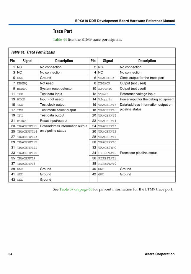
EPXA10 DDR Development Board Hardware Reference Manual
Trace Port
Table 44 lists the ETM9 trace port signals
See Table 57 on page 66 for pin-out information for the ETM9 trace port
Table 44 Trace Port Signals
Pin Signal Description Pin Signal Description
1 NC No connection 2 NC No connection
3 NC No connection 4 NC No connection
5 GND Ground 6 TRACECLK Clock output for the trace port
7 DBGRQ Not used 8 DBGACK Output (not used)
9 nSRST System reset detector 10 EXTTRIG Output (not used)
11 TDO Test data input 12 VTRef Reference voltage input
13 RTCK Input (not used) 14 VSupply Power input for the debug equipment
15 TCK Test clock output 16 TRACEPKT7 Dataaddress information output on pipeline status17 TMS Test mode select output 18 TRACEPKT6
19 TDI Test data output 20 TRACEPKT5
21 nTRST Reset inputoutput 22 TRACEPKT4
23 TRACEPKT15 Dataaddress information output on pipeline status
24 TRACEPKT3
25 TRACEPKT14 26 TRACEPKT2
27 TRACEPKT13 28 TRACEPKT1
29 TRACEPKT12 30 TRACEPKT0
31 TRACEPKT11 32 TRACESYNC
33 TRACEPKT10 34 PIPESTAT2 Processor pipeline status
35 TRACEPKT9 36 PIPESTAT1
37 TRACEPKT8 38 PIPESTAT0
39 GND Ground 40 GND Ground
41 GND Ground 42 GND Ground
43 GND Ground
54 Altera Corporation
EPXA10 DDR Development Board Hardware Reference Manual
ConfigurationDebugging Interfaces
On the development board there are interfaces for a MasterBlaster or ByteBlasterMV cable and a Multi-ICE connector Table 45 lists the signals on the MasterBlasterByteBlasterMV interface
See Table 47 on page 58 for pin-out information for the development board configuration and debugging interfaces
Table 45 MasterBlasterByteBlasterMV Female Interface
Pin JTAG Mode
Signal Description
1 TCK Clock signal
2 GND Signal ground
3 TDO Data from device
4 Vcc Power supply
5 TMS JTAG state machine control
6 Vio Reference voltage for MasterBlasterByteBlasterMV output driver
7 TCK Clock signal
8 ndash No connection
9 TDI Data to device
10 GND Signal ground
Altera Corporation 55
EPXA10 DDR Development Board Hardware Reference Manual
Table 46 lists the signals on the Multi-ICE interface
See Table 47 on page 58 for pin-out information for the development board configuration and debugging interfaces
f For signal details of the EPC16 device refer to the EPC16 pin-out table
See Table 57 on page 66 for pin-out information for the trace port
Table 46 Multi-ICE Connector
Pin Signal Description Direction
1 Vcc Power supply NA
2 Vcc Power supply NA
3 PROC_NTRTS Processor reset O
4 GND Ground NA
5 PROC_TDI Processor test data input I
6 GND Ground NA
7 PROC_TMS Processor test mode select I
8 GND Ground NA
9 PROC_TCK Processor test clock input I
10 GND Ground NA
11 GND Ground NA
12 GND Ground NA
13 PROC_TDO Processor test data output O
14 GND Ground NA
15 NSRST Warm reset IO
16 GND Ground NA
17 NC No connection NA
18 GND Ground NA
19 NA No connection NA
20 GND Ground NA
56 Altera Corporation
EPXA10 DDR Development Board Hardware Reference Manual
Pin-Outs The main component of the development board is the EPXA10F1020C1 device The pins on the EPXA10 device are assigned to functions on the board When generating IP cores for the EPXA10 device the pins must be used as defined to avoid damaging the device and any unused pins must be tri-stated using the Quartus II software The following sections list the interfaces and dedicated pins on the board Any pins not used for a design should be left in the high-impedance (input) state to avoid contention
This section details the EPXA10 device pins that are assigned to the following purposes
Configuration DDR SDRAM EBI UARTs 1 and 2 Ethernet User LEDs push buttons and dip-switches Fast IO pins IDC 10-pin header Trace port Test points
Pin assignments are grouped into tables for control pins bank address pins and data bus pins where appropriate The tables also detail signals passing across a connection The remaining IO pins on the EPXA10 device are listed at the end of this section
Configuration
The EPXA10 device pins listed in Table 47 on page 58 are used exclusively for configuring the device Refer to ldquoDevice Configurationrdquo on page 41 for more information about EPXA10 configuration
Altera Corporation 57
EPXA10 DDR Development Board Hardware Reference Manual
Table 47 EPXA10 Device Configuration Pins
Signal Name EPXA10 Device Pin Description
MSEL0 J30 Configuration mode select (tied to GND)
MSEL1 K30 Configuration mode select (tied to GND)
NSTATUS AM14 OE for EPC16
NCONFIG R30 n_INIT_CONF for EPC16
DCLK W3 Data clock for EPC16
CONF_DONE AM13 Configuration complete indicator
INIT_DONE D14 Initialization complete indicator
nCE AC3 Not connected
nCEO D13
DATA0 V3 Serial input for EPC16 configuration data
DATA1 D10 Serial input for EPC16 configuration data available for user IO after configurationDATA2 A9
DATA3 B9
DATA4 C9
DATA5 D9
DATA6 A4
DATA7 B4
TDI AD3 JTAG data input
TDO E11 JTAG data output (to next device in the chain
TCK AM19 JTAG clock
TMS AM20 JTAG mode select
TRST C13 JTAG reset (pulled high)
PROC_TDI H27 JTAG data input
PROC_TDO H26 JTAG data output (to next device in the chain
PROC_TCK D30 JTAG clock
PROC_TMS E29 JTAG mode select
PROC_TRST E30 JTAG reset (pulled high)
DEV_CLRn H3 Global reset for the device
DEV_OE AE3 Device output enable
nWS C4 Write strobe
nRS D4 Read strobe
nCS D3 Signal providing handshaking between devices
CS E3 Chip select
RDYnBSY E14 Readybusy
CLKUSR A13 Clock signal
58 Altera Corporation
EPXA10 DDR Development Board Hardware Reference Manual
DDR SDRAM Interface
There are four DDR chips (256-Mbit times 8) on the EPXA10 DDR development board selectable using one chip-select SD_CS0_N The development board DDR interface can run at up to 266 MHz
f For more details on how to use the DDR SDRAM ref to AN141 Using the SDRAM Controller
Table 48 lists the pin-outs for the DDR SDRAM control signals
Table 49 on page 60 lists the DDR SDRAM data bank and address bus pin-outs
Table 48 DDR SDRAM Control Signal Pin-Outs
Signal Name EPXA10 Device Pin Description
SD_RAS_N F17 Row address strobe
SD_CAS_N F18 Column address strobe
SD_WE_N G18 Write enable
SD_CS0_N G14 Chip select
SD_CS1_N F16 Chip select
SD_CLKE F14 Clock enable
SD_CLK F15 SDRAM clock
SD_CLK_N G13 SDRAM clock - inverted
SD_DQM(0) H14 Data byte mask
SD_DQM(1) L14 Data byte mask
SD_DQM(2) K9 Data byte mask
SD_DQM(3) H9 Data byte mask
SD_DQS(0) J14 DQS signal
SD_DQS(1) K14 DQS signal
SD_DQS(2) K10 DQS signal
SD_DQS(3) H10 DQS signal
Altera Corporation 59
EPXA10 DDR Development Board Hardware Reference Manual
Table 49 DDR SDRAM Data Bank amp Address Bus Pin-Outs
Signal Name EPXA10 Device Pin
Signal Name EPXA10 Device Pin
Signal Name EPXA10 Device Pin
SD_DQ0 H18 SD_DQ1 H17 SD_DQ2 H16
SD_DQ3 J18 SD_DQ4 J17 SD_DQ5 H15
SD_DQ6 J16 SD_DQ7 J15 SD_DQ8 K18
SD_DQ9 K17 SD_DQ10 L18 SD_DQ11 K16
SD_DQ12 L17 SD_DQ13 L16 SD_DQ14 K15
SD_DQ15 L15 SD_DQ16 L13 SD_DQ17 K13
SD_DQ18 L12 SD_DQ19 K12 SD_DQ20 L11
SD_DQ21 K11 SD_DQ22 L10 SD_DQ23 L9
SD_DQ24 H13 SD_DQ25 H12 SD_DQ26 J13
SD_DQ27 J12 SD_DQ28 J11 SD_DQ29 J10
SD_DQ30 J9 SD_DQ31 H11 SD_ADD0 G12
SD_ADD1 F13 SD_ADD2 G11 SD_ADD3 F12
SD_ADD4 F11 SD_ADD5 G10 SD_ADD6 F10
SD_ADD7 F9 SD_ADD8 G9 SD_ADD9 F8
SD_ADD10 G8 SD_ADD11 F7 SD_ADD12 F6
SD_ADD13 G7 SD_ADD14 G6
60 Altera Corporation
EPXA10 DDR Development Board Hardware Reference Manual
EBI
Table 50 lists the EPXA10 pin-outs for the EBI control signals
Table 50 EBI Control Signal Pin-Outs
Signal Name EPXA10 Device Pin Description
EBI_BE0 F27 Byte enable
EBI_BE1 E27 Byte enable
EBI_OE F26 Output enable
EBI_WE E26 Write enable
EBI_CS0 A25 Chip select
EBI_CS1 B25 Chip select
EBI_CS2 C25 Chip select
EBI_CS3 D25 Chip select
EBI_CLK E25 EBI clock
EBI_ACK F25 EBI acknowledge
INT_EXTPIN_N G25 Interrupt generated by push-button SW4
Altera Corporation 61
EPXA10 DDR Development Board Hardware Reference Manual
Table 51 lists the EBI data bank and address bus pin-outs
Table 51 EBI Data Bank and Address Bus Pin-Outs
Signal Name EPXA10 Device Pin
Signal Name EPXA10 Device Pin
EBI_DQ0 J21 EBI_DQ1 H21
EBI_DQ2 E20 EBI_DQ3 F20
EBI_DQ4 E19 EBI_DQ5 L20
EBI_DQ6 K20 EBI_DQ7 J20
EBI_DQ8 H20 EBI_DQ9 G20
EBI_DQ10 F19 EBI_DQ11 G19
EBI_DQ12 L19 EBI_DQ13 K19
EBI_DQ14 J19 EBI_DQ15 H19
EBI_A0 H25 EBI_A1 D24
EBI_A2 E24 EBI_A3 F24
EBI_A4 G24 EBI_A5 J24
EBI_A6 H24 EBI_A7 E23
EBI_A8 F23 EBI_A9 G23
EBI_A10 K23 EBI_A11 J23
EBI_A12 H23 EBI_A13 E22
EBI_A14 F22 EBI_A15 E21
EBI_A16 L22 EBI_A17 K22
EBI_A18 J22 EBI_A19 H22
EBI_A20 G22 EBI_A21 F21
EBI_A22 G21 EBI_A23 L21
EBI_A24 K21
62 Altera Corporation
EPXA10 DDR Development Board Hardware Reference Manual
PCI
Table 52 lists the pins used for the PCI cards
Table 52 PCI Pin-Outs
FPGA UART Embedded Stripe UART
EPXA10 Device Pin
Device Signal (Board Signal)
EPXA10 Device Pin
Device Signal (Board Signal)
AF21 CBE0 AF22 A5 (PCI_BUS5)
AE19 CBE1 AG22 A6 (PCI_BUS6)
AF19 CBE2 AH22 A7 (PCI_BUS7)
AJ18 CBE3 AD21 A8 (PCI_BUS8)
AG19 DEVSEL AE21 A9 (PCI_BUS9)
AH19 FRAME AG21 A10 (PCI_BUS10)
AB20 GNT1 AH21 A11 (PCI_BUS11)
AC20 GNT2 AD20 A12 (PCI_BUS12)
AB22 INTA AE20 A13 (PCI_BUS13)
AG23 INTB AF20 A14 (PCI_BUS14)
AC22 INTC AH20 A15 (PCI_BUS15)
AF23 INTD AJ19 A16 (PCI_BUS16)
AK20 PAR AK19 A17 (PCI_BUS17)
AB18 PCI_RST AL19 A18 (PCI_BUS18)
AL18 PERR AD18 A19 (PCI_BUS19)
AB21 PRSNT1 AE18 A20 (PCI_BUS20)
AC22 PRSNT2 AF18 A21 (PCI_BUS21)
AD19 REQ1 AG18 A22 (PCI_BUS22)
AC19 REQ2 AH18 A23 (PCI_BUS23)
AB19 SERR AK18 A24 (PCI_BUS24)
AB17 STOP AC17 A25 (PCI_BUS25)
AC18 TRDY AD17 A26 (PCI_BUS26)
AK23 A0 (PCI_BUS0) AE17 A27 (PCI_BUS27)
AL23 A1 (PCI_BUS1) AF17 A28 (PCI_BUS28)
AM23 A2 (PCI_BUS2) AG17 A29 (PCI_BUS29)
AD22 A3 (PCI_BUS3) AH17 A30 (PCI_BUS30)
AE22 A4 (PCI_BUS4) AJ17 A31 (PCI_BUS31)
Altera Corporation 63
EPXA10 DDR Development Board Hardware Reference Manual
UART1 amp UART2
Table 53 lists the pins used for UARTs 1 and 2
Ethernet
Table 53 lists the pins used for the Ethernet interface
Table 53 Extension Header UARTs 1 amp 2 IO Pin-Outs
FPGA UART Embedded Stripe UART
EPXA10 Device Pin
Device Signal Expansion Board Connector
EPXA10 Device Pin
Device Signal Expansion Board Connector
J27 UART2_DTR_N U16171 G28 UART1_CTS_N NC
J29 UART2_TXD U16174 D29 UART1_RXD NC
K29 UART2_RXD_N U16177 E28 UART1_RI_N NC
K27 UART2_DSR_N U16179 C28 UART1_RTS_N NC
J28 UART2_RTS_N U16173 F28 UART1_DSR_N NC
J26 UART2_RI_N U16175 G27 UART1_DCD_N NC
K28 UART2_DCD_N U16178 D28 UART1_TXD NC
K26 UART2_CTS_N U16181 G26 UART1_DTR_N NC
Table 54 Extension Header Ethernet Pin-Outs
EPXA10 Device Pin
Device Signal Expansion Board Connector
EPXA10 Device Pin
Device Signal Expansion Board Connector
R23 RXD1 U16155 R24 TXD3 U16153
R25 TXD0 U16149 M19 MDC U16145
M20 RST_N U16146 M21 TX_ER U16161
M22 TX_EN U16162 M23 RXD2 U16157
N19 CRS U16166 N20 COL U16163
N21 RX_DV U16167 N22 MDIO U16169
N23 RXD0 U16154 P20 INTR U16147
P21 RX_ER U16165 P22 RX_D3 U16158
N25 TXD1 U16150 P25 TXD2 U16151
64 Altera Corporation
EPXA10 DDR Development Board Hardware Reference Manual
Fast IO Pins
Table 55 lists the pins used for the EPXA10 fast IO pins
User LEDs Switches amp Push Button Switches
Table 56 lists the pins used for the user-defined LEDs push-button switches and dip-switches
Table 55 EPXA10 Fast IO Pins
EPXA10 Pin Name
Description EPXA10 Device Pin
Expansion Board Connector
Board Reference
FAST0 Dedicated fast IO pins E13 U16133 FAST0
FAST1 Dedicated fast IO pins E12 U16134 FAST1
FAST2 Dedicated fast IO pins AM18 U16135 FAST2
FAST3 Connected to PCI to provide IRDY AM15 IRDY
Table 56 Expansion Header LED Switch and Push Button IO Pin-Outs
EPXA10 Device Pin
Device Signal Expansion Board Connector
EPXA10 Device Pin
Device Signal Board Connector
V6 USER_LED0 U181 U5 USER_LED1 U183
V5 USER_LED2 U184 U6 USER_LED3 U185
V7 USER_LED4 U187 V8 USER_LED5 U188
U7 USER_LED6 U189 T6 USER_LED7 U1811
U8 USER_SW0 U1812 T5 USER_SW1 U1813
V4 USER_SW2 U1815 V10 USER_SW3 U1816
T7 USER_SW4 U1817 W12 USER_SW5 U1817
U9 USER_SW6 U1820 V11 USER_SW7 U1821
R6 USER-SW8 U1823 T8 USER_PB0 U1824
R5 USER_PB1 U1825 U4 USER_PB2 U1827
U10 USER_PB3 U1828
Altera Corporation 65
EPXA10 DDR Development Board Hardware Reference Manual
Trace Port
Table 57 lists the pins used on the trace port interface
IDC 10-Pin Header
Table 56 lists the pins used for the 10-pin IDC header
Table 57 Trace Port Pin-Out
EPXA10 Device Pin
Device Signal EPXA10 Device Pin
Device Signal
H6 TRACEPKT15 N7 TRACEPKT4
J6 TRACEPKT14 H8 TRACEPKT3
K6 TRACEPKT13 J8 TRACEPKT2
L6 TRACEPKT12 K8 TRACEPKT1
M6 TRACEPKT11 L8 TRACEPKT0
N6 TRACEPKT10 M8 TRACESYNC
H7 TRACEPKT9 M9 PIPESTAT2
J7 TRACEPKT8 N9 PIPESTAT1
K7 TRACEPKT7 N10 PIPESTAT0
L7 TRACEPKT6 N8 TRACECLK
M7 TRACEPKT5
Table 58 IDC Header Pin-Outs
EPXA10 Device Pin Header Pin Expansion Board Connector
L5 Header11 U1871
K4 Header12 U1872
J4 Header13 U1873
H4 Header14 U1875
K5 Header15 U1876
E4 Header16 U1877
J5 Header17 U1879
H5 Header18 U1880
GND Header19 na
GND Header110 na
66 Altera Corporation
EPXA10 DDR Development Board Hardware Reference Manual
Expansion Header
The pins on the expansion header cards connect to IO pins on the EPXA10 device to ground or to VCC supplies
IO Pin-Outs
Tables 59 to 62 list the pins on the EPXA10 DDR development board expansion header cards that connect to IO pins on the EPXA10 device Some of these pins can optionally be dedicated to the Ethernet UART user LEDs push-button switches and dip-switches
Table 59 Development Board Expansion Header U15 IO Pin-Outs (Part 1 of 2)
U151-50 Device U1551-100 Device U15101-150
Device U15151-200
Device
U151 AB24 U1551 AC23 U15101 GND U15151 Y5
U152 GND U1552 AD23 U15102 W4 U15152 Y8
U153 L24 U1553 AE23 U15103 W5 U15153 GND
U154 L26 U1554 GND U15104 AA6 U15154 Y7
U155 L27 U1555 AL20 U15105 GND U15155 Y4
U156 GND U1556 AJ20 U15106 W8 U15156 B24
U157 AJ29 U1557 AG20 U15107 Y6 U15157 GND
U158 AK29 U1558 GND U15108 W7 U15158 A24
U159 AH28 U1559 AJ30 U15109 GND U15159 D23
U1510 GND U1560 IOData7 U15110 W6 U15160 C23
U1511 AJ28 U1561 IOData6 U15111 AF5 U15161 GND
U1512 AK28 U1562 GND U15112 AE4 U15162 B23
U1513 AH27 U1563 IOData5 U15113 GND U15163 A23
U1514 GND U1564 IOData4 U15114 AD4 U15164 D20
U1515 AH26 U1565 IOData3 U15115 AC4 U15165 GND
U1516 AG26 U1566 GND U15116 AE5 U15166 C20
U1517 AF26 U1567 IOData2 U15117 GND U15167 B20
U1518 GND U1568 IOData1 U15118 AD8 U15168 A20
U1519 AM25(1) U1569 N26 U15119 AA12 U15169 GND
U1520 AL25 U1570 GND U15120 AC9 U15170 D19
U1521 AK25(1) U1571 N29 U15121 GND U15171 C19
U1522 GND U1572 IOCLKUSR U15122 AD5 U15172 B19
U1523 AJ25(1) U1573 IORDYNBSY U15123 AC5 U15173 GND
U1524 AH25 U1574 GND U15124 AD7 U15174 A19
U1525 AG25 U1575 NRS U15125 GND U15175 A18
Altera Corporation 67
EPXA10 DDR Development Board Hardware Reference Manual
U1526 GND U1576 IONWS U15126 AA11 U15176 B18
U1527 AF25 U1577 IONCS U15127 Y12 U15177 GND
U1528 AE25 U1578 GND U15128 AC8 U15178 D18
U1529 AD25 U1579 IOCS U15129 GND U15179 E18
U1530 GND U1580 M25 U15130 AB5 U15180 D17
U1531 AC25 U1580 M26 U15131 AB9 U15181 GND
U1532 AB25 U1581 P27 U15132 AA10 U15182 E17
U1533 AM24 U1582 GND U15133 GND U15183 D16
U1534 GND U1583 M28 U15134 Y11 U15184 E16
U1535 AL24 U1584 NC U15135 AD6 U15185 GND
U1536 AK24 U1585 NC U15136 AA5 U15186 D15
U1537 AJ24 U1586 GND U15137 GND U15187 B15
U1538 GND U1587 NCLK3 U15138 AC7 U15188 A15
U1539 AH24 U1588 GND U15139 AB8 U15189 GND
U1540 AC24 U1589 NCLK4 U15140 Y10 U15190 B14
U1541 AD24 U1590 GND U15141 GND U15191 A14
U1542 GND U1591 CLK2_OUT U15142 W11 U15192 E15
U1543 AE24 U1592 GND U15143 AA8 U15193 GND
U1544 AF24 U1593 NCLK2_FB U15144 AB7 U15194 C14
U1545 AG24 U1594 GND U15145 GND U15195 NCLK1_FB
U1546 GND U1595 CLK2_FBP U15146 AC6 U15196 GND
U1547 AJ23 U1596 GND U15147 W10 U15197 CLK1_FBP
U1548 AH23 U1597 NCLK2 U15148 AA7 U15198 GND
U1549 AB23 U1598 GND U15149 GND U15199 NCLK1
U1550 GND U1599 CLK1_OUT U15150 AB6 U15200 GND
Table 59 Development Board Expansion Header U15 IO Pin-Outs (Part 2 of 2)
U151-50 Device U1551-100 Device U15101-150
Device U15151-200
Device
68 Altera Corporation
EPXA10 DDR Development Board Hardware Reference Manual
Table 60 Development Board Expansion Header U16 IO Pin-Outs (Part 1 of 2)
U161-50 Device U1651-100
Device U16101-150
Device U16151-200
Device
U161 GND U1651 AD2 U16101 IOLVDSDSKW U16151 P25
U162 AE3 U1652 GND U16102 GND U16152 GND
U163 AK5 U1653 AE1 U16103 W32 U16153 R24
U164 GND U1654 AE2 U16104 W31 U16154 N23
U165 AM5 U1655 GND U16105 GND U16155 R23
U166 AL5 U1656 AH1 U16106 V31 U16156 GND
U167 GND U1657 AH2 U16107 V32 U16157 M23
U168 AK4 U1658 GND U16108 GND U16158 P22
U169 AJ3 U1659 AJ1 U16109 R32 U16159 NC
U1610 GND U1660 AJ2 U16110 R31 U16160 GND
U1611 AL4 U1661 GND U16111 GND U16161 M21
U1612 AM4 U1662 B29 U16112 P31 U16162 M22
U1613 GND U1663 A29 U16113 P32 U16163 N20
U1614 D1 U1664 GND U16114 GND U16164 GND
U1615 D2 U1665 AJ32 U16115 N32 U16165 P21
U1616 GND U1666 AJ31 U16116 N31 U16166 N19
U1617 E1 U1667 GND U16117 GND U16167 N21
U1618 E2 U1668 AH31 U16118 K31 U16168 GND
U1619 GND U1669 AH32 U16119 K32 U16169 N22
U1620 H1 U1670 GND U16120 GND U16170 J26
U1621 H2 U1671 AE32 U16121 J32 U16171 J27
U1622 GND U1672 AE31 U16122 J31 U16172 GND
U1623 J1 U1673 GND U16123 GND U16173 J28
U1624 J2 U1674 AD31 U16124 H31 U16174 J29
U1625 GND U1675 AD32 U16125 H32 U16175 UART2_RI_N
U1626 K1 U1676 GND U16126 GND U16176 GND
U1627 K2 U1677 AC32 U16127 E32 U16177 K29
U1628 GND U1678 AC31 U16128 E31 U16178 K28
U1629 N2 U1679 GND U16129 GND U16179 K27
U1630 N1 U1680 Y31 U16130 D31 U16180 GND
U1631 GND U1681 Y32 U16131 D32 U16181 K26
U1632 P1 U1682 GND U16132 GND U16182 L28
U1633 P2 U1683 AC30 U16133 FAST0 U16183 L23
U1634 GND U1684 AL29 U16134 FAST1 U16184 GND
Altera Corporation 69
EPXA10 DDR Development Board Hardware Reference Manual
U1635 R1 U1685 H30 U16135 FAST2 U16185 GND
U1636 R2 U1686 GND U16136 GND U16186 12V
U1637 GND U1687 5V U16137 R26 U16187 33V
U1638 V1 U1688 33V U16138 R27 U16188 12V-
U1639 V2 U1689 5V U16139 R28 U16189 33V
U1640 GND U1690 33V U16140 GND U16190 12V-
U1641 W1 U1691 5V U16141 R29 U16191 33V
U1642 W2 U1692 33V U16142 P28 U16192 12V
U1643 GND U1693 5V U16143 P29 U16193 33V
U1644 Y2 U1694 33V U16144 GND U16194 12V
U1645 Y1 U1695 5V U16145 M19 U16195 33V
U1646 GND U1696 33V U16146 M20 U16196 12V
U1647 AC1 U1697 5V U16147 P20 U16197 33V
U1648 AC2 U1698 33V U16148 GND U16198 12V
U1649 GND U1699 5V U16149 R25 U16199 33V
U1650 AD1 U16100 33V U16150 N25 U16200 12V
Table 60 Development Board Expansion Header U16 IO Pin-Outs (Part 2 of 2)
U161-50 Device U1651-100
Device U16101-150
Device U16151-200
Device
70 Altera Corporation
EPXA10 DDR Development Board Hardware Reference Manual
Table 61 Development Board Expansion Header U17 IO Pin-Outs (Part 1 of 2)
U171-50 Device U1751-100 Device U17101-150
Device U17151-200
Device
U171 AC11 U1751 AJ5 U17101 GND U17151 W22
U172 GND U1752 AH5 U17102 NC U17152 V21
U173 AB11 U1753 AJ4 U17103 NRESET U17153 GND
U174 AH10 U1754 GND U17104 NC U17154 AA28
U175 AJ10 U1755 AH4 U17105 GND U17155 AC27
U176 GND U1756 AG5 U17106 NC U17156 AB26
U177 AK10 U1757 T27 U17107 NC U17157 GND
U178 AL10 U1758 GND U17108 NC U17158 AA25
U179 AG10 U1759 U27 U17109 GND U17159 Y24
U1710 GND U1760 V27 U17110 NC U17160 W23
U1711 AF10 U1761 V26 U17111 NC U17161 GND
U1712 AE10 U1762 GND U17112 NC U17162 V22
U1713 AD10 U1763 T29 U17113 GND U17163 U21
U1714 GND U1764 T28 U17114 AG28 U17164 AB28
U1715 AC10 U1765 T26 U17115 AH29 U17165 GND
U1716 AB10 U1766 GND U17116 AG27 U17166 Y28
U1717 AH9 U1767 U26 U17117 GND U17167 AB27
U1718 GND U1768 W27 U17118 AH30 U17168 AA26
U1719 AJ9 U1769 T25 U17119 AF27 U17169 GND
U1720 AK9 U1770 GND U17120 AF28 U17170 Y25
U1721 AL9 U1771 U25 U17121 GND U17171 V23
U1722 GND U1772 U29 U17122 AE26 U17172 U22
U1723 AM9 U1773 U28 U17123 AE27 U17173 GND
U1724 AG9 U1774 GND U17124 AE30 U17174 T21
U1725 AF9 U1775 R22 U17125 GND U17175 W28
U1726 GND U1776 Y27 U17126 AE29 U17176 W29
U1727 AE9 U1777 W26 U17127 AE28 U17177 GND
U1728 AD9 U1778 GND U17128 AA21 U17178 R20
U1729 AM8 U1779 V25 U17129 GND U17179 T22
U1730 GND U1780 U24 U17130 AD26 U17180 AA27
U1731 AL8 U1781 T23 U17131 AD30 U17181 GND
U1732 AK8 U1782 GND U17132 AD29 U17182 Y26
U1733 AJ8 U1783 R21 U17133 GND U17183 W25
U1734 GND U1784 V29 U17134 AC29 U17184 U23
Altera Corporation 71
EPXA10 DDR Development Board Hardware Reference Manual
U1735 AH8 U1785 V28 U17135 AA22 U17185 GND
U1736 AG8 U1786 GND U17136 AD27 U17186 12V
U1737 AF8 U1787 5V U17137 GND U17187 33V
U1738 GND U1788 33V U17138 AD28 U17188 12V-
U1739 AE8 U1789 5V U17139 Y29 U17189 33V
U1740 AH7 U1790 33V U17140 Y21 U17190 12V-
U1741 AF7 U1791 5V U17141 GND U17191 33V
U1742 GND U1792 33V U17142 AA23 U17192 12V
U1743 AG7 U1793 5V U17143 AC28 U17193 33V
U1744 AE7 U1794 33V U17144 AC26 U17194 12V
U1745 AH6 U1795 5V U17145 GND U17195 33V
U1746 GND U1796 33V U17146 Y22 U17196 12V
U1747 AG6 U1797 5V U17147 W21 U17197 33V
U1748 AF6 U1798 33V U17148 AA24 U17198 12V
U1749 AE6 U1799 5V U17149 GND U17199 33V
U1750 GND U17100 33V U17150 Y23 U17200 12V
Table 61 Development Board Expansion Header U17 IO Pin-Outs (Part 2 of 2)
U171-50 Device U1751-100 Device U17101-150
Device U17151-200
Device
72 Altera Corporation
EPXA10 DDR Development Board Hardware Reference Manual
Table 62 Development Board Expansion Header U18 IO Pin-Outs (Part 1 of 2)
U181-50 Device U1851-100 Device U18101-150
Device U18151-200
Device
U181 V6 U1851 N5 U18101 GND U18151 AF13
U182 GND U1852 R10 U18102 AK17 U18152 AG13
U183 U5 U1853 R11 U18103 AK16 U18153 GND
U184 V5 U1854 GND U18104 AJ16 U18154 AB13
U185 U6 U1855 R12 U18105 GND U18155 AH12
U186 GND U1856 R13 U18106 AH16 U18156 AE12
U187 V7 U1857 P10 U18107 AG16 U18157 GND
U188 V8 U1858 GND U18108 AF16 U18158 AF12
U189 U7 U1859 P11 U18109 GND U18159 AG12
U1810 GND U1860 P12 U18110 AE16 U18160 AG11
U1811 T6 U1861 P13 U18111 AD16 U18161 GND
U1812 U8 U1862 GND U18112 AC16 U18162 AD12
U1813 T5 U1863 P4 U18113 GND U18163 AF11
U1814 GND U1864 N4 U18114 AB16 U18164 AH11
U1815 V4 U1865 N11 U18115 AL15 U18165 GND
U1816 V10 U1866 GND U18116 AK15 U18166 AC12
U1817 T7 U1867 N12 U18117 GND U18167 AE11
U1817 W12 U1868 N13 U18118 AJ15 U18168 AB12
U1818 GND U1869 M5 U18119 AH15 U18169 GND
U1819 USER_SW5 U1870 GND U18120 AG15 U18170 AD11
U1820 U9 U1871 L5 U18121 GND U18171 A8
U1821 V11 U1872 K4 U18122 AF15 U18172 E6
U1822 GND U1873 J4 U18123 AE15 U18173 GND
U1823 R6 U1874 GND U18124 AD15 U18174 E7
U1824 T8 U1875 H4 U18125 GND U18175 C8
U1825 R5 U1876 K5 U18126 AC15 U18176 B8
U1826 GND U1877 E4 U18127 AB15 U18177 GND
U1827 U4 U1878 GND U18128 AL14 U18178 E9
U1828 U10 U1879 J5 U18129 GND U18179 E8
U1829 R7 U1880 H5 U18130 AK14 U18180 D8
U1830 GND U1881 G5 U18131 AJ14 U18181 GND
U1831 V12 U1882 GND U18132 AH14 U18182 B5
U1832 U11 U1883 F5 U18133 GND U18183 A5
U1833 R8 U1884 E5 U18134 AG14 U18184 E10
Altera Corporation 73
EPXA10 DDR Development Board Hardware Reference Manual
GND Connections
Table 59 lists the pins on the EPXA10 DDR development board expansion header cards that connect to GND
U1834 GND U1885 D5 U18135 AF14 U18185 GND
U1835 P6 U1886 GND U18136 AE14 U18186 12V
U1836 T4 U1887 5V U18137 GND U18187 33V
U1837 P5 U1888 33V U18138 AD14 U18188 12V-
U1838 GND U1889 5V U18139 AC14 U18189 33V
U1839 T10 U1890 33V U18140 AB14 U18190 12V-
U1840 U12 U1891 5V U18141 GND U18191 33V
U1841 T11 U1892 33V U18142 AL13 U18192 12V
U1842 GND U1893 5V U18143 AK13 U18193 33V
U1843 P7 U1894 33V U18144 AJ13 U18194 12V
U1844 R9 U1895 5V U18145 GND U18195 33V
U1845 T12 U1896 33V U18146 AH13 U18196 12V
U1846 GND U1897 5V U18147 AC13 U18197 33V
U1847 T13 U1898 33V U18148 AD13 U18198 12V
U1848 P8 U1899 5V U18149 GND U18199 33V
U1849 R4 U18100 33V U18150 AE13 U18200 12V
U1850 GND U1851 N5 U18101 GND U18151 AF13
Table 62 Development Board Expansion Header U18 IO Pin-Outs (Part 2 of 2)
U181-50 Device U1851-100 Device U18101-150
Device U18151-200
Device
Table 63 Development Board Expansion Header GND Connections
Header Pin
U15 2 6 10 14 18 22 26 30 34 38 42 46 50 54 58 62 66 70 74 78 82 86 88 90 92 94 96 98 100 101 105 109 113 117 121 125 129 133 137 141 145 149 153 157 161 165 169 173 177 181 185 189 193 196 198 200
U16 1 4 7 10 13 16 19 22 25 28 31 34 37 40 43 46 49 52 55 58 61 64 67 70 73 76 79 82 86 102 105 108 111 114 117 120 123 126 129 132 136 140 144 148 152 156 160 164 168 172 176 180 184 185
U17 2 6 10 14 18 22 26 30 34 38 42 46 50 54 58 62 66 70 74 78 82 86 101 105 109 113 117 121 125 129 133 137 141 145 149 153 157 161 165 169 173 177 181 185
U18 2 6 10 14 18 22 26 30 34 38 42 46 50 54 58 62 66 70 74 78 82 86 101 105 109 113 117 121 125 129 133 137 141 145 149 153 157 161 165 169 173 177 181 185
74 Altera Corporation
EPXA10 DDR Development Board Hardware Reference Manual
VCC Connections
Table 59 lists the pins on the EPXA10 DDR development board expansion header cards that connect to VCC power supplies
Table 64 Development Board Expansion Header VC C Connections
Expansion Header
VC C Pin
U16 33 V 88 90 92 94 96 98 100 187 189 191 193 195 197 199
5 V 87 89 91 93 95 97 99
12 V 186 192 194 196 198 200
ndash12 V 188 190
U17 33 V 88 90 92 94 96 98 100 187 189 191 193 195 197 199
5 V 87 89 91 93 95 97 99
12 V 186 192 194 196 198 200
ndash12 V 188 190
U18 33 V 88 90 92 94 96 98 100 187 189 191 193 195 197 199
5 V 87 89 91 93 95 97 99
12 V 186 192 194 196 198 200
ndash12 V 188 190
Altera Corporation 75
EPXA10 DDR Development Board Hardware Reference Manual
General Usage Guidelines
To use the development board properly and to avoid damage to it follow the guidelines in this section
Anti-Static Handling
Before handling the card you should take proper anti-static precautions otherwise the board can be damaged
Power-Up
When power is initially applied to the board the LEDs flash according to the software test running on the embedded processor The test suite is programmed directly into flash memory and when the embedded processor boots it configures the FPGA and runs the software using the test image
Power Consumption
Power consumption issues need to be addressed only if the board is powered from a terminal strip and not the provided ATX power supply adaptor Altera recommends that you monitor the input current to ensure that sufficient power is supplied The power required by the board is directly related to the following
Number of interfaces used Density and speed of the device Population of the interfaces
The typical maximum current is 50 A which can be exceeded if the board is heavily loaded with many interfaces running at high-clock speeds
PCI Cards
1 Do not use 5-V PCI cards
The PCI slots on the development board are suitable only for 33-V and universal PCI cards The keying slots on 5-V PCI cards are not designed to mate with the motherboard connectors because the signalling voltage on 5-V cards is incorrect for the development board
76 Altera Corporation
EPXA10 DDR Development Board Hardware Reference Manual
Unused EPXA10 Device Pins
All unused general-purpose IO EPXA10 device pins have been allocated to the expansion headers To avoid unnecessary power consumption and possible contention unused pins must be left in the high impedance (input) state Follow the steps below to put the unused EPXA10 device pins into a high-impedance state
1 Run the Quartus II software
2 Choose Compiler Settings (Processing menu)
3 Click the Chips amp Devices tag
4 Click the Device amp Pin Options button
5 Click the Unused Pins tag
6 Under Reserve all unused pins select As inputs tri-stated
All the critical control lines for the interfaces on the board are pulled to the inactive state
1 If a device is not used it can be ignored and the EPXA10 device interface pins left as inputs
Test Core Functionality
For implementing a test plan Altera provides test cores with the development board which can be programmed onto the EPXA10 device using the JTAG chain Each test core tests one or more interfaces (push-buttons LEDs switches etc) Diagnostic software is also provided to test the board the EPXA10 device and its test cores with results displayed on a terminal
Altera Corporation 77
EPXA10 DDR Development Board Hardware Reference Manual
78 Altera Corporation
- EPXA10 DDR Development Board Hardware Reference Manual
-
- How to Find Information
- How to Contact Altera
- Typographic Conventions
- Features
- Functional Overview
- Board Components
- Interfaces
-
- PCI Interface
-
- EPXA10 Device Signal Definitions for PCI Cards
- Board-Level Issues
-
- 10100 Ethernet Parallel Interface
-
- Ethernet LEDs
- Ethernet Switches
-
- Serial IO Interfaces
- Memory Interfaces
-
- DDR SDRAM
- Flash Memory
-
- LED amp Switch Interfaces
-
- User-Defined LEDs
- Function-Specific LEDs
- Switch Interfaces
-
- Trace Port Interface
- 10-Pin IDC Header Interface
- Expansion Header Interface
-
- Jumper Configuration
- Clocks
-
- CLK_REF amp the FPGA Clocks
- MAX 3032
- Embedded Stripe Clocks
- Jumper Configuration for the Clock Input
- Sources for the EPXA10 Clocks
-
- Using an External Clock Generator
- Using the Main Clock
- Using a Variable Oscillator
-
- Device Configuration
-
- Booting from Flash Memory
- Configuring Using the EPC16
- Configuring Using JTAG
- Configuration Schemes
-
- EPC16 Configuration Device
- MasterBlasterByteBlasterMV Communications Cable
-
- Debugging Features
-
- Third-Party Debugging Tools
- JTAG Interfaces
-
- Using JSELECT
- Using MasterBlasterByteBlasterMV Cable to Program the EPC16 Device
-
- Power Supply
-
- Test Points
- Signals
-
- UART
- PCI
- Trace Port
- ConfigurationDebugging Interfaces
-
- Pin-Outs
-
- Configuration
- DDR SDRAM Interface
- EBI
- PCI
- UART1 amp UART2
- Ethernet
- Fast IO Pins
- User LEDs Switches amp Push Button Switches
- Trace Port
- IDC 10-Pin Header
- Expansion Header
-
- IO Pin-Outs
- GND Connections
- VCC Connections
-
- General Usage Guidelines
-
- Anti-Static Handling
- Power-Up
- Power Consumption
- PCI Cards
- Unused EPXA10 Device Pins
- Test Core Functionality
-

EPXA10 DDR Development Board Hardware Reference Manual
Table 51 lists the EBI data bank and address bus pin-outs
Table 51 EBI Data Bank and Address Bus Pin-Outs
Signal Name EPXA10 Device Pin
Signal Name EPXA10 Device Pin
EBI_DQ0 J21 EBI_DQ1 H21
EBI_DQ2 E20 EBI_DQ3 F20
EBI_DQ4 E19 EBI_DQ5 L20
EBI_DQ6 K20 EBI_DQ7 J20
EBI_DQ8 H20 EBI_DQ9 G20
EBI_DQ10 F19 EBI_DQ11 G19
EBI_DQ12 L19 EBI_DQ13 K19
EBI_DQ14 J19 EBI_DQ15 H19
EBI_A0 H25 EBI_A1 D24
EBI_A2 E24 EBI_A3 F24
EBI_A4 G24 EBI_A5 J24
EBI_A6 H24 EBI_A7 E23
EBI_A8 F23 EBI_A9 G23
EBI_A10 K23 EBI_A11 J23
EBI_A12 H23 EBI_A13 E22
EBI_A14 F22 EBI_A15 E21
EBI_A16 L22 EBI_A17 K22
EBI_A18 J22 EBI_A19 H22
EBI_A20 G22 EBI_A21 F21
EBI_A22 G21 EBI_A23 L21
EBI_A24 K21
62 Altera Corporation
EPXA10 DDR Development Board Hardware Reference Manual
PCI
Table 52 lists the pins used for the PCI cards
Table 52 PCI Pin-Outs
FPGA UART Embedded Stripe UART
EPXA10 Device Pin
Device Signal (Board Signal)
EPXA10 Device Pin
Device Signal (Board Signal)
AF21 CBE0 AF22 A5 (PCI_BUS5)
AE19 CBE1 AG22 A6 (PCI_BUS6)
AF19 CBE2 AH22 A7 (PCI_BUS7)
AJ18 CBE3 AD21 A8 (PCI_BUS8)
AG19 DEVSEL AE21 A9 (PCI_BUS9)
AH19 FRAME AG21 A10 (PCI_BUS10)
AB20 GNT1 AH21 A11 (PCI_BUS11)
AC20 GNT2 AD20 A12 (PCI_BUS12)
AB22 INTA AE20 A13 (PCI_BUS13)
AG23 INTB AF20 A14 (PCI_BUS14)
AC22 INTC AH20 A15 (PCI_BUS15)
AF23 INTD AJ19 A16 (PCI_BUS16)
AK20 PAR AK19 A17 (PCI_BUS17)
AB18 PCI_RST AL19 A18 (PCI_BUS18)
AL18 PERR AD18 A19 (PCI_BUS19)
AB21 PRSNT1 AE18 A20 (PCI_BUS20)
AC22 PRSNT2 AF18 A21 (PCI_BUS21)
AD19 REQ1 AG18 A22 (PCI_BUS22)
AC19 REQ2 AH18 A23 (PCI_BUS23)
AB19 SERR AK18 A24 (PCI_BUS24)
AB17 STOP AC17 A25 (PCI_BUS25)
AC18 TRDY AD17 A26 (PCI_BUS26)
AK23 A0 (PCI_BUS0) AE17 A27 (PCI_BUS27)
AL23 A1 (PCI_BUS1) AF17 A28 (PCI_BUS28)
AM23 A2 (PCI_BUS2) AG17 A29 (PCI_BUS29)
AD22 A3 (PCI_BUS3) AH17 A30 (PCI_BUS30)
AE22 A4 (PCI_BUS4) AJ17 A31 (PCI_BUS31)
Altera Corporation 63
EPXA10 DDR Development Board Hardware Reference Manual
UART1 amp UART2
Table 53 lists the pins used for UARTs 1 and 2
Ethernet
Table 53 lists the pins used for the Ethernet interface
Table 53 Extension Header UARTs 1 amp 2 IO Pin-Outs
FPGA UART Embedded Stripe UART
EPXA10 Device Pin
Device Signal Expansion Board Connector
EPXA10 Device Pin
Device Signal Expansion Board Connector
J27 UART2_DTR_N U16171 G28 UART1_CTS_N NC
J29 UART2_TXD U16174 D29 UART1_RXD NC
K29 UART2_RXD_N U16177 E28 UART1_RI_N NC
K27 UART2_DSR_N U16179 C28 UART1_RTS_N NC
J28 UART2_RTS_N U16173 F28 UART1_DSR_N NC
J26 UART2_RI_N U16175 G27 UART1_DCD_N NC
K28 UART2_DCD_N U16178 D28 UART1_TXD NC
K26 UART2_CTS_N U16181 G26 UART1_DTR_N NC
Table 54 Extension Header Ethernet Pin-Outs
EPXA10 Device Pin
Device Signal Expansion Board Connector
EPXA10 Device Pin
Device Signal Expansion Board Connector
R23 RXD1 U16155 R24 TXD3 U16153
R25 TXD0 U16149 M19 MDC U16145
M20 RST_N U16146 M21 TX_ER U16161
M22 TX_EN U16162 M23 RXD2 U16157
N19 CRS U16166 N20 COL U16163
N21 RX_DV U16167 N22 MDIO U16169
N23 RXD0 U16154 P20 INTR U16147
P21 RX_ER U16165 P22 RX_D3 U16158
N25 TXD1 U16150 P25 TXD2 U16151
64 Altera Corporation
EPXA10 DDR Development Board Hardware Reference Manual
Fast IO Pins
Table 55 lists the pins used for the EPXA10 fast IO pins
User LEDs Switches amp Push Button Switches
Table 56 lists the pins used for the user-defined LEDs push-button switches and dip-switches
Table 55 EPXA10 Fast IO Pins
EPXA10 Pin Name
Description EPXA10 Device Pin
Expansion Board Connector
Board Reference
FAST0 Dedicated fast IO pins E13 U16133 FAST0
FAST1 Dedicated fast IO pins E12 U16134 FAST1
FAST2 Dedicated fast IO pins AM18 U16135 FAST2
FAST3 Connected to PCI to provide IRDY AM15 IRDY
Table 56 Expansion Header LED Switch and Push Button IO Pin-Outs
EPXA10 Device Pin
Device Signal Expansion Board Connector
EPXA10 Device Pin
Device Signal Board Connector
V6 USER_LED0 U181 U5 USER_LED1 U183
V5 USER_LED2 U184 U6 USER_LED3 U185
V7 USER_LED4 U187 V8 USER_LED5 U188
U7 USER_LED6 U189 T6 USER_LED7 U1811
U8 USER_SW0 U1812 T5 USER_SW1 U1813
V4 USER_SW2 U1815 V10 USER_SW3 U1816
T7 USER_SW4 U1817 W12 USER_SW5 U1817
U9 USER_SW6 U1820 V11 USER_SW7 U1821
R6 USER-SW8 U1823 T8 USER_PB0 U1824
R5 USER_PB1 U1825 U4 USER_PB2 U1827
U10 USER_PB3 U1828
Altera Corporation 65
EPXA10 DDR Development Board Hardware Reference Manual
Trace Port
Table 57 lists the pins used on the trace port interface
IDC 10-Pin Header
Table 56 lists the pins used for the 10-pin IDC header
Table 57 Trace Port Pin-Out
EPXA10 Device Pin
Device Signal EPXA10 Device Pin
Device Signal
H6 TRACEPKT15 N7 TRACEPKT4
J6 TRACEPKT14 H8 TRACEPKT3
K6 TRACEPKT13 J8 TRACEPKT2
L6 TRACEPKT12 K8 TRACEPKT1
M6 TRACEPKT11 L8 TRACEPKT0
N6 TRACEPKT10 M8 TRACESYNC
H7 TRACEPKT9 M9 PIPESTAT2
J7 TRACEPKT8 N9 PIPESTAT1
K7 TRACEPKT7 N10 PIPESTAT0
L7 TRACEPKT6 N8 TRACECLK
M7 TRACEPKT5
Table 58 IDC Header Pin-Outs
EPXA10 Device Pin Header Pin Expansion Board Connector
L5 Header11 U1871
K4 Header12 U1872
J4 Header13 U1873
H4 Header14 U1875
K5 Header15 U1876
E4 Header16 U1877
J5 Header17 U1879
H5 Header18 U1880
GND Header19 na
GND Header110 na
66 Altera Corporation
EPXA10 DDR Development Board Hardware Reference Manual
Expansion Header
The pins on the expansion header cards connect to IO pins on the EPXA10 device to ground or to VCC supplies
IO Pin-Outs
Tables 59 to 62 list the pins on the EPXA10 DDR development board expansion header cards that connect to IO pins on the EPXA10 device Some of these pins can optionally be dedicated to the Ethernet UART user LEDs push-button switches and dip-switches
Table 59 Development Board Expansion Header U15 IO Pin-Outs (Part 1 of 2)
U151-50 Device U1551-100 Device U15101-150
Device U15151-200
Device
U151 AB24 U1551 AC23 U15101 GND U15151 Y5
U152 GND U1552 AD23 U15102 W4 U15152 Y8
U153 L24 U1553 AE23 U15103 W5 U15153 GND
U154 L26 U1554 GND U15104 AA6 U15154 Y7
U155 L27 U1555 AL20 U15105 GND U15155 Y4
U156 GND U1556 AJ20 U15106 W8 U15156 B24
U157 AJ29 U1557 AG20 U15107 Y6 U15157 GND
U158 AK29 U1558 GND U15108 W7 U15158 A24
U159 AH28 U1559 AJ30 U15109 GND U15159 D23
U1510 GND U1560 IOData7 U15110 W6 U15160 C23
U1511 AJ28 U1561 IOData6 U15111 AF5 U15161 GND
U1512 AK28 U1562 GND U15112 AE4 U15162 B23
U1513 AH27 U1563 IOData5 U15113 GND U15163 A23
U1514 GND U1564 IOData4 U15114 AD4 U15164 D20
U1515 AH26 U1565 IOData3 U15115 AC4 U15165 GND
U1516 AG26 U1566 GND U15116 AE5 U15166 C20
U1517 AF26 U1567 IOData2 U15117 GND U15167 B20
U1518 GND U1568 IOData1 U15118 AD8 U15168 A20
U1519 AM25(1) U1569 N26 U15119 AA12 U15169 GND
U1520 AL25 U1570 GND U15120 AC9 U15170 D19
U1521 AK25(1) U1571 N29 U15121 GND U15171 C19
U1522 GND U1572 IOCLKUSR U15122 AD5 U15172 B19
U1523 AJ25(1) U1573 IORDYNBSY U15123 AC5 U15173 GND
U1524 AH25 U1574 GND U15124 AD7 U15174 A19
U1525 AG25 U1575 NRS U15125 GND U15175 A18
Altera Corporation 67
EPXA10 DDR Development Board Hardware Reference Manual
U1526 GND U1576 IONWS U15126 AA11 U15176 B18
U1527 AF25 U1577 IONCS U15127 Y12 U15177 GND
U1528 AE25 U1578 GND U15128 AC8 U15178 D18
U1529 AD25 U1579 IOCS U15129 GND U15179 E18
U1530 GND U1580 M25 U15130 AB5 U15180 D17
U1531 AC25 U1580 M26 U15131 AB9 U15181 GND
U1532 AB25 U1581 P27 U15132 AA10 U15182 E17
U1533 AM24 U1582 GND U15133 GND U15183 D16
U1534 GND U1583 M28 U15134 Y11 U15184 E16
U1535 AL24 U1584 NC U15135 AD6 U15185 GND
U1536 AK24 U1585 NC U15136 AA5 U15186 D15
U1537 AJ24 U1586 GND U15137 GND U15187 B15
U1538 GND U1587 NCLK3 U15138 AC7 U15188 A15
U1539 AH24 U1588 GND U15139 AB8 U15189 GND
U1540 AC24 U1589 NCLK4 U15140 Y10 U15190 B14
U1541 AD24 U1590 GND U15141 GND U15191 A14
U1542 GND U1591 CLK2_OUT U15142 W11 U15192 E15
U1543 AE24 U1592 GND U15143 AA8 U15193 GND
U1544 AF24 U1593 NCLK2_FB U15144 AB7 U15194 C14
U1545 AG24 U1594 GND U15145 GND U15195 NCLK1_FB
U1546 GND U1595 CLK2_FBP U15146 AC6 U15196 GND
U1547 AJ23 U1596 GND U15147 W10 U15197 CLK1_FBP
U1548 AH23 U1597 NCLK2 U15148 AA7 U15198 GND
U1549 AB23 U1598 GND U15149 GND U15199 NCLK1
U1550 GND U1599 CLK1_OUT U15150 AB6 U15200 GND
Table 59 Development Board Expansion Header U15 IO Pin-Outs (Part 2 of 2)
U151-50 Device U1551-100 Device U15101-150
Device U15151-200
Device
68 Altera Corporation
EPXA10 DDR Development Board Hardware Reference Manual
Table 60 Development Board Expansion Header U16 IO Pin-Outs (Part 1 of 2)
U161-50 Device U1651-100
Device U16101-150
Device U16151-200
Device
U161 GND U1651 AD2 U16101 IOLVDSDSKW U16151 P25
U162 AE3 U1652 GND U16102 GND U16152 GND
U163 AK5 U1653 AE1 U16103 W32 U16153 R24
U164 GND U1654 AE2 U16104 W31 U16154 N23
U165 AM5 U1655 GND U16105 GND U16155 R23
U166 AL5 U1656 AH1 U16106 V31 U16156 GND
U167 GND U1657 AH2 U16107 V32 U16157 M23
U168 AK4 U1658 GND U16108 GND U16158 P22
U169 AJ3 U1659 AJ1 U16109 R32 U16159 NC
U1610 GND U1660 AJ2 U16110 R31 U16160 GND
U1611 AL4 U1661 GND U16111 GND U16161 M21
U1612 AM4 U1662 B29 U16112 P31 U16162 M22
U1613 GND U1663 A29 U16113 P32 U16163 N20
U1614 D1 U1664 GND U16114 GND U16164 GND
U1615 D2 U1665 AJ32 U16115 N32 U16165 P21
U1616 GND U1666 AJ31 U16116 N31 U16166 N19
U1617 E1 U1667 GND U16117 GND U16167 N21
U1618 E2 U1668 AH31 U16118 K31 U16168 GND
U1619 GND U1669 AH32 U16119 K32 U16169 N22
U1620 H1 U1670 GND U16120 GND U16170 J26
U1621 H2 U1671 AE32 U16121 J32 U16171 J27
U1622 GND U1672 AE31 U16122 J31 U16172 GND
U1623 J1 U1673 GND U16123 GND U16173 J28
U1624 J2 U1674 AD31 U16124 H31 U16174 J29
U1625 GND U1675 AD32 U16125 H32 U16175 UART2_RI_N
U1626 K1 U1676 GND U16126 GND U16176 GND
U1627 K2 U1677 AC32 U16127 E32 U16177 K29
U1628 GND U1678 AC31 U16128 E31 U16178 K28
U1629 N2 U1679 GND U16129 GND U16179 K27
U1630 N1 U1680 Y31 U16130 D31 U16180 GND
U1631 GND U1681 Y32 U16131 D32 U16181 K26
U1632 P1 U1682 GND U16132 GND U16182 L28
U1633 P2 U1683 AC30 U16133 FAST0 U16183 L23
U1634 GND U1684 AL29 U16134 FAST1 U16184 GND
Altera Corporation 69
EPXA10 DDR Development Board Hardware Reference Manual
U1635 R1 U1685 H30 U16135 FAST2 U16185 GND
U1636 R2 U1686 GND U16136 GND U16186 12V
U1637 GND U1687 5V U16137 R26 U16187 33V
U1638 V1 U1688 33V U16138 R27 U16188 12V-
U1639 V2 U1689 5V U16139 R28 U16189 33V
U1640 GND U1690 33V U16140 GND U16190 12V-
U1641 W1 U1691 5V U16141 R29 U16191 33V
U1642 W2 U1692 33V U16142 P28 U16192 12V
U1643 GND U1693 5V U16143 P29 U16193 33V
U1644 Y2 U1694 33V U16144 GND U16194 12V
U1645 Y1 U1695 5V U16145 M19 U16195 33V
U1646 GND U1696 33V U16146 M20 U16196 12V
U1647 AC1 U1697 5V U16147 P20 U16197 33V
U1648 AC2 U1698 33V U16148 GND U16198 12V
U1649 GND U1699 5V U16149 R25 U16199 33V
U1650 AD1 U16100 33V U16150 N25 U16200 12V
Table 60 Development Board Expansion Header U16 IO Pin-Outs (Part 2 of 2)
U161-50 Device U1651-100
Device U16101-150
Device U16151-200
Device
70 Altera Corporation
EPXA10 DDR Development Board Hardware Reference Manual
Table 61 Development Board Expansion Header U17 IO Pin-Outs (Part 1 of 2)
U171-50 Device U1751-100 Device U17101-150
Device U17151-200
Device
U171 AC11 U1751 AJ5 U17101 GND U17151 W22
U172 GND U1752 AH5 U17102 NC U17152 V21
U173 AB11 U1753 AJ4 U17103 NRESET U17153 GND
U174 AH10 U1754 GND U17104 NC U17154 AA28
U175 AJ10 U1755 AH4 U17105 GND U17155 AC27
U176 GND U1756 AG5 U17106 NC U17156 AB26
U177 AK10 U1757 T27 U17107 NC U17157 GND
U178 AL10 U1758 GND U17108 NC U17158 AA25
U179 AG10 U1759 U27 U17109 GND U17159 Y24
U1710 GND U1760 V27 U17110 NC U17160 W23
U1711 AF10 U1761 V26 U17111 NC U17161 GND
U1712 AE10 U1762 GND U17112 NC U17162 V22
U1713 AD10 U1763 T29 U17113 GND U17163 U21
U1714 GND U1764 T28 U17114 AG28 U17164 AB28
U1715 AC10 U1765 T26 U17115 AH29 U17165 GND
U1716 AB10 U1766 GND U17116 AG27 U17166 Y28
U1717 AH9 U1767 U26 U17117 GND U17167 AB27
U1718 GND U1768 W27 U17118 AH30 U17168 AA26
U1719 AJ9 U1769 T25 U17119 AF27 U17169 GND
U1720 AK9 U1770 GND U17120 AF28 U17170 Y25
U1721 AL9 U1771 U25 U17121 GND U17171 V23
U1722 GND U1772 U29 U17122 AE26 U17172 U22
U1723 AM9 U1773 U28 U17123 AE27 U17173 GND
U1724 AG9 U1774 GND U17124 AE30 U17174 T21
U1725 AF9 U1775 R22 U17125 GND U17175 W28
U1726 GND U1776 Y27 U17126 AE29 U17176 W29
U1727 AE9 U1777 W26 U17127 AE28 U17177 GND
U1728 AD9 U1778 GND U17128 AA21 U17178 R20
U1729 AM8 U1779 V25 U17129 GND U17179 T22
U1730 GND U1780 U24 U17130 AD26 U17180 AA27
U1731 AL8 U1781 T23 U17131 AD30 U17181 GND
U1732 AK8 U1782 GND U17132 AD29 U17182 Y26
U1733 AJ8 U1783 R21 U17133 GND U17183 W25
U1734 GND U1784 V29 U17134 AC29 U17184 U23
Altera Corporation 71
EPXA10 DDR Development Board Hardware Reference Manual
U1735 AH8 U1785 V28 U17135 AA22 U17185 GND
U1736 AG8 U1786 GND U17136 AD27 U17186 12V
U1737 AF8 U1787 5V U17137 GND U17187 33V
U1738 GND U1788 33V U17138 AD28 U17188 12V-
U1739 AE8 U1789 5V U17139 Y29 U17189 33V
U1740 AH7 U1790 33V U17140 Y21 U17190 12V-
U1741 AF7 U1791 5V U17141 GND U17191 33V
U1742 GND U1792 33V U17142 AA23 U17192 12V
U1743 AG7 U1793 5V U17143 AC28 U17193 33V
U1744 AE7 U1794 33V U17144 AC26 U17194 12V
U1745 AH6 U1795 5V U17145 GND U17195 33V
U1746 GND U1796 33V U17146 Y22 U17196 12V
U1747 AG6 U1797 5V U17147 W21 U17197 33V
U1748 AF6 U1798 33V U17148 AA24 U17198 12V
U1749 AE6 U1799 5V U17149 GND U17199 33V
U1750 GND U17100 33V U17150 Y23 U17200 12V
Table 61 Development Board Expansion Header U17 IO Pin-Outs (Part 2 of 2)
U171-50 Device U1751-100 Device U17101-150
Device U17151-200
Device
72 Altera Corporation
EPXA10 DDR Development Board Hardware Reference Manual
Table 62 Development Board Expansion Header U18 IO Pin-Outs (Part 1 of 2)
U181-50 Device U1851-100 Device U18101-150
Device U18151-200
Device
U181 V6 U1851 N5 U18101 GND U18151 AF13
U182 GND U1852 R10 U18102 AK17 U18152 AG13
U183 U5 U1853 R11 U18103 AK16 U18153 GND
U184 V5 U1854 GND U18104 AJ16 U18154 AB13
U185 U6 U1855 R12 U18105 GND U18155 AH12
U186 GND U1856 R13 U18106 AH16 U18156 AE12
U187 V7 U1857 P10 U18107 AG16 U18157 GND
U188 V8 U1858 GND U18108 AF16 U18158 AF12
U189 U7 U1859 P11 U18109 GND U18159 AG12
U1810 GND U1860 P12 U18110 AE16 U18160 AG11
U1811 T6 U1861 P13 U18111 AD16 U18161 GND
U1812 U8 U1862 GND U18112 AC16 U18162 AD12
U1813 T5 U1863 P4 U18113 GND U18163 AF11
U1814 GND U1864 N4 U18114 AB16 U18164 AH11
U1815 V4 U1865 N11 U18115 AL15 U18165 GND
U1816 V10 U1866 GND U18116 AK15 U18166 AC12
U1817 T7 U1867 N12 U18117 GND U18167 AE11
U1817 W12 U1868 N13 U18118 AJ15 U18168 AB12
U1818 GND U1869 M5 U18119 AH15 U18169 GND
U1819 USER_SW5 U1870 GND U18120 AG15 U18170 AD11
U1820 U9 U1871 L5 U18121 GND U18171 A8
U1821 V11 U1872 K4 U18122 AF15 U18172 E6
U1822 GND U1873 J4 U18123 AE15 U18173 GND
U1823 R6 U1874 GND U18124 AD15 U18174 E7
U1824 T8 U1875 H4 U18125 GND U18175 C8
U1825 R5 U1876 K5 U18126 AC15 U18176 B8
U1826 GND U1877 E4 U18127 AB15 U18177 GND
U1827 U4 U1878 GND U18128 AL14 U18178 E9
U1828 U10 U1879 J5 U18129 GND U18179 E8
U1829 R7 U1880 H5 U18130 AK14 U18180 D8
U1830 GND U1881 G5 U18131 AJ14 U18181 GND
U1831 V12 U1882 GND U18132 AH14 U18182 B5
U1832 U11 U1883 F5 U18133 GND U18183 A5
U1833 R8 U1884 E5 U18134 AG14 U18184 E10
Altera Corporation 73
EPXA10 DDR Development Board Hardware Reference Manual
GND Connections
Table 59 lists the pins on the EPXA10 DDR development board expansion header cards that connect to GND
U1834 GND U1885 D5 U18135 AF14 U18185 GND
U1835 P6 U1886 GND U18136 AE14 U18186 12V
U1836 T4 U1887 5V U18137 GND U18187 33V
U1837 P5 U1888 33V U18138 AD14 U18188 12V-
U1838 GND U1889 5V U18139 AC14 U18189 33V
U1839 T10 U1890 33V U18140 AB14 U18190 12V-
U1840 U12 U1891 5V U18141 GND U18191 33V
U1841 T11 U1892 33V U18142 AL13 U18192 12V
U1842 GND U1893 5V U18143 AK13 U18193 33V
U1843 P7 U1894 33V U18144 AJ13 U18194 12V
U1844 R9 U1895 5V U18145 GND U18195 33V
U1845 T12 U1896 33V U18146 AH13 U18196 12V
U1846 GND U1897 5V U18147 AC13 U18197 33V
U1847 T13 U1898 33V U18148 AD13 U18198 12V
U1848 P8 U1899 5V U18149 GND U18199 33V
U1849 R4 U18100 33V U18150 AE13 U18200 12V
U1850 GND U1851 N5 U18101 GND U18151 AF13
Table 62 Development Board Expansion Header U18 IO Pin-Outs (Part 2 of 2)
U181-50 Device U1851-100 Device U18101-150
Device U18151-200
Device
Table 63 Development Board Expansion Header GND Connections
Header Pin
U15 2 6 10 14 18 22 26 30 34 38 42 46 50 54 58 62 66 70 74 78 82 86 88 90 92 94 96 98 100 101 105 109 113 117 121 125 129 133 137 141 145 149 153 157 161 165 169 173 177 181 185 189 193 196 198 200
U16 1 4 7 10 13 16 19 22 25 28 31 34 37 40 43 46 49 52 55 58 61 64 67 70 73 76 79 82 86 102 105 108 111 114 117 120 123 126 129 132 136 140 144 148 152 156 160 164 168 172 176 180 184 185
U17 2 6 10 14 18 22 26 30 34 38 42 46 50 54 58 62 66 70 74 78 82 86 101 105 109 113 117 121 125 129 133 137 141 145 149 153 157 161 165 169 173 177 181 185
U18 2 6 10 14 18 22 26 30 34 38 42 46 50 54 58 62 66 70 74 78 82 86 101 105 109 113 117 121 125 129 133 137 141 145 149 153 157 161 165 169 173 177 181 185
74 Altera Corporation
EPXA10 DDR Development Board Hardware Reference Manual
VCC Connections
Table 59 lists the pins on the EPXA10 DDR development board expansion header cards that connect to VCC power supplies
Table 64 Development Board Expansion Header VC C Connections
Expansion Header
VC C Pin
U16 33 V 88 90 92 94 96 98 100 187 189 191 193 195 197 199
5 V 87 89 91 93 95 97 99
12 V 186 192 194 196 198 200
ndash12 V 188 190
U17 33 V 88 90 92 94 96 98 100 187 189 191 193 195 197 199
5 V 87 89 91 93 95 97 99
12 V 186 192 194 196 198 200
ndash12 V 188 190
U18 33 V 88 90 92 94 96 98 100 187 189 191 193 195 197 199
5 V 87 89 91 93 95 97 99
12 V 186 192 194 196 198 200
ndash12 V 188 190
Altera Corporation 75
EPXA10 DDR Development Board Hardware Reference Manual
General Usage Guidelines
To use the development board properly and to avoid damage to it follow the guidelines in this section
Anti-Static Handling
Before handling the card you should take proper anti-static precautions otherwise the board can be damaged
Power-Up
When power is initially applied to the board the LEDs flash according to the software test running on the embedded processor The test suite is programmed directly into flash memory and when the embedded processor boots it configures the FPGA and runs the software using the test image
Power Consumption
Power consumption issues need to be addressed only if the board is powered from a terminal strip and not the provided ATX power supply adaptor Altera recommends that you monitor the input current to ensure that sufficient power is supplied The power required by the board is directly related to the following
Number of interfaces used Density and speed of the device Population of the interfaces
The typical maximum current is 50 A which can be exceeded if the board is heavily loaded with many interfaces running at high-clock speeds
PCI Cards
1 Do not use 5-V PCI cards
The PCI slots on the development board are suitable only for 33-V and universal PCI cards The keying slots on 5-V PCI cards are not designed to mate with the motherboard connectors because the signalling voltage on 5-V cards is incorrect for the development board
76 Altera Corporation
EPXA10 DDR Development Board Hardware Reference Manual
Unused EPXA10 Device Pins
All unused general-purpose IO EPXA10 device pins have been allocated to the expansion headers To avoid unnecessary power consumption and possible contention unused pins must be left in the high impedance (input) state Follow the steps below to put the unused EPXA10 device pins into a high-impedance state
1 Run the Quartus II software
2 Choose Compiler Settings (Processing menu)
3 Click the Chips amp Devices tag
4 Click the Device amp Pin Options button
5 Click the Unused Pins tag
6 Under Reserve all unused pins select As inputs tri-stated
All the critical control lines for the interfaces on the board are pulled to the inactive state
1 If a device is not used it can be ignored and the EPXA10 device interface pins left as inputs
Test Core Functionality
For implementing a test plan Altera provides test cores with the development board which can be programmed onto the EPXA10 device using the JTAG chain Each test core tests one or more interfaces (push-buttons LEDs switches etc) Diagnostic software is also provided to test the board the EPXA10 device and its test cores with results displayed on a terminal
Altera Corporation 77
EPXA10 DDR Development Board Hardware Reference Manual
78 Altera Corporation
- EPXA10 DDR Development Board Hardware Reference Manual
-
- How to Find Information
- How to Contact Altera
- Typographic Conventions
- Features
- Functional Overview
- Board Components
- Interfaces
-
- PCI Interface
-
- EPXA10 Device Signal Definitions for PCI Cards
- Board-Level Issues
-
- 10100 Ethernet Parallel Interface
-
- Ethernet LEDs
- Ethernet Switches
-
- Serial IO Interfaces
- Memory Interfaces
-
- DDR SDRAM
- Flash Memory
-
- LED amp Switch Interfaces
-
- User-Defined LEDs
- Function-Specific LEDs
- Switch Interfaces
-
- Trace Port Interface
- 10-Pin IDC Header Interface
- Expansion Header Interface
-
- Jumper Configuration
- Clocks
-
- CLK_REF amp the FPGA Clocks
- MAX 3032
- Embedded Stripe Clocks
- Jumper Configuration for the Clock Input
- Sources for the EPXA10 Clocks
-
- Using an External Clock Generator
- Using the Main Clock
- Using a Variable Oscillator
-
- Device Configuration
-
- Booting from Flash Memory
- Configuring Using the EPC16
- Configuring Using JTAG
- Configuration Schemes
-
- EPC16 Configuration Device
- MasterBlasterByteBlasterMV Communications Cable
-
- Debugging Features
-
- Third-Party Debugging Tools
- JTAG Interfaces
-
- Using JSELECT
- Using MasterBlasterByteBlasterMV Cable to Program the EPC16 Device
-
- Power Supply
-
- Test Points
- Signals
-
- UART
- PCI
- Trace Port
- ConfigurationDebugging Interfaces
-
- Pin-Outs
-
- Configuration
- DDR SDRAM Interface
- EBI
- PCI
- UART1 amp UART2
- Ethernet
- Fast IO Pins
- User LEDs Switches amp Push Button Switches
- Trace Port
- IDC 10-Pin Header
- Expansion Header
-
- IO Pin-Outs
- GND Connections
- VCC Connections
-
- General Usage Guidelines
-
- Anti-Static Handling
- Power-Up
- Power Consumption
- PCI Cards
- Unused EPXA10 Device Pins
- Test Core Functionality
-
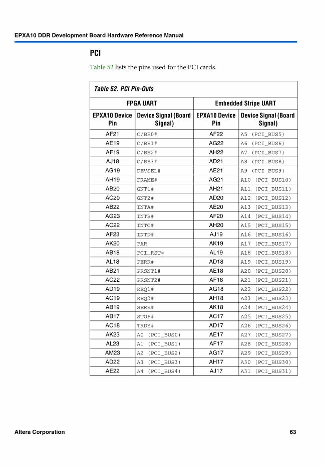
EPXA10 DDR Development Board Hardware Reference Manual
Expansion Header
The pins on the expansion header cards connect to IO pins on the EPXA10 device to ground or to VCC supplies
IO Pin-Outs
Tables 59 to 62 list the pins on the EPXA10 DDR development board expansion header cards that connect to IO pins on the EPXA10 device Some of these pins can optionally be dedicated to the Ethernet UART user LEDs push-button switches and dip-switches
Table 59 Development Board Expansion Header U15 IO Pin-Outs (Part 1 of 2)
U151-50 Device U1551-100 Device U15101-150
Device U15151-200
Device
U151 AB24 U1551 AC23 U15101 GND U15151 Y5
U152 GND U1552 AD23 U15102 W4 U15152 Y8
U153 L24 U1553 AE23 U15103 W5 U15153 GND
U154 L26 U1554 GND U15104 AA6 U15154 Y7
U155 L27 U1555 AL20 U15105 GND U15155 Y4
U156 GND U1556 AJ20 U15106 W8 U15156 B24
U157 AJ29 U1557 AG20 U15107 Y6 U15157 GND
U158 AK29 U1558 GND U15108 W7 U15158 A24
U159 AH28 U1559 AJ30 U15109 GND U15159 D23
U1510 GND U1560 IOData7 U15110 W6 U15160 C23
U1511 AJ28 U1561 IOData6 U15111 AF5 U15161 GND
U1512 AK28 U1562 GND U15112 AE4 U15162 B23
U1513 AH27 U1563 IOData5 U15113 GND U15163 A23
U1514 GND U1564 IOData4 U15114 AD4 U15164 D20
U1515 AH26 U1565 IOData3 U15115 AC4 U15165 GND
U1516 AG26 U1566 GND U15116 AE5 U15166 C20
U1517 AF26 U1567 IOData2 U15117 GND U15167 B20
U1518 GND U1568 IOData1 U15118 AD8 U15168 A20
U1519 AM25(1) U1569 N26 U15119 AA12 U15169 GND
U1520 AL25 U1570 GND U15120 AC9 U15170 D19
U1521 AK25(1) U1571 N29 U15121 GND U15171 C19
U1522 GND U1572 IOCLKUSR U15122 AD5 U15172 B19
U1523 AJ25(1) U1573 IORDYNBSY U15123 AC5 U15173 GND
U1524 AH25 U1574 GND U15124 AD7 U15174 A19
U1525 AG25 U1575 NRS U15125 GND U15175 A18
Altera Corporation 67
EPXA10 DDR Development Board Hardware Reference Manual
U1526 GND U1576 IONWS U15126 AA11 U15176 B18
U1527 AF25 U1577 IONCS U15127 Y12 U15177 GND
U1528 AE25 U1578 GND U15128 AC8 U15178 D18
U1529 AD25 U1579 IOCS U15129 GND U15179 E18
U1530 GND U1580 M25 U15130 AB5 U15180 D17
U1531 AC25 U1580 M26 U15131 AB9 U15181 GND
U1532 AB25 U1581 P27 U15132 AA10 U15182 E17
U1533 AM24 U1582 GND U15133 GND U15183 D16
U1534 GND U1583 M28 U15134 Y11 U15184 E16
U1535 AL24 U1584 NC U15135 AD6 U15185 GND
U1536 AK24 U1585 NC U15136 AA5 U15186 D15
U1537 AJ24 U1586 GND U15137 GND U15187 B15
U1538 GND U1587 NCLK3 U15138 AC7 U15188 A15
U1539 AH24 U1588 GND U15139 AB8 U15189 GND
U1540 AC24 U1589 NCLK4 U15140 Y10 U15190 B14
U1541 AD24 U1590 GND U15141 GND U15191 A14
U1542 GND U1591 CLK2_OUT U15142 W11 U15192 E15
U1543 AE24 U1592 GND U15143 AA8 U15193 GND
U1544 AF24 U1593 NCLK2_FB U15144 AB7 U15194 C14
U1545 AG24 U1594 GND U15145 GND U15195 NCLK1_FB
U1546 GND U1595 CLK2_FBP U15146 AC6 U15196 GND
U1547 AJ23 U1596 GND U15147 W10 U15197 CLK1_FBP
U1548 AH23 U1597 NCLK2 U15148 AA7 U15198 GND
U1549 AB23 U1598 GND U15149 GND U15199 NCLK1
U1550 GND U1599 CLK1_OUT U15150 AB6 U15200 GND
Table 59 Development Board Expansion Header U15 IO Pin-Outs (Part 2 of 2)
U151-50 Device U1551-100 Device U15101-150
Device U15151-200
Device
68 Altera Corporation
EPXA10 DDR Development Board Hardware Reference Manual
Table 60 Development Board Expansion Header U16 IO Pin-Outs (Part 1 of 2)
U161-50 Device U1651-100
Device U16101-150
Device U16151-200
Device
U161 GND U1651 AD2 U16101 IOLVDSDSKW U16151 P25
U162 AE3 U1652 GND U16102 GND U16152 GND
U163 AK5 U1653 AE1 U16103 W32 U16153 R24
U164 GND U1654 AE2 U16104 W31 U16154 N23
U165 AM5 U1655 GND U16105 GND U16155 R23
U166 AL5 U1656 AH1 U16106 V31 U16156 GND
U167 GND U1657 AH2 U16107 V32 U16157 M23
U168 AK4 U1658 GND U16108 GND U16158 P22
U169 AJ3 U1659 AJ1 U16109 R32 U16159 NC
U1610 GND U1660 AJ2 U16110 R31 U16160 GND
U1611 AL4 U1661 GND U16111 GND U16161 M21
U1612 AM4 U1662 B29 U16112 P31 U16162 M22
U1613 GND U1663 A29 U16113 P32 U16163 N20
U1614 D1 U1664 GND U16114 GND U16164 GND
U1615 D2 U1665 AJ32 U16115 N32 U16165 P21
U1616 GND U1666 AJ31 U16116 N31 U16166 N19
U1617 E1 U1667 GND U16117 GND U16167 N21
U1618 E2 U1668 AH31 U16118 K31 U16168 GND
U1619 GND U1669 AH32 U16119 K32 U16169 N22
U1620 H1 U1670 GND U16120 GND U16170 J26
U1621 H2 U1671 AE32 U16121 J32 U16171 J27
U1622 GND U1672 AE31 U16122 J31 U16172 GND
U1623 J1 U1673 GND U16123 GND U16173 J28
U1624 J2 U1674 AD31 U16124 H31 U16174 J29
U1625 GND U1675 AD32 U16125 H32 U16175 UART2_RI_N
U1626 K1 U1676 GND U16126 GND U16176 GND
U1627 K2 U1677 AC32 U16127 E32 U16177 K29
U1628 GND U1678 AC31 U16128 E31 U16178 K28
U1629 N2 U1679 GND U16129 GND U16179 K27
U1630 N1 U1680 Y31 U16130 D31 U16180 GND
U1631 GND U1681 Y32 U16131 D32 U16181 K26
U1632 P1 U1682 GND U16132 GND U16182 L28
U1633 P2 U1683 AC30 U16133 FAST0 U16183 L23
U1634 GND U1684 AL29 U16134 FAST1 U16184 GND
Altera Corporation 69
EPXA10 DDR Development Board Hardware Reference Manual
U1635 R1 U1685 H30 U16135 FAST2 U16185 GND
U1636 R2 U1686 GND U16136 GND U16186 12V
U1637 GND U1687 5V U16137 R26 U16187 33V
U1638 V1 U1688 33V U16138 R27 U16188 12V-
U1639 V2 U1689 5V U16139 R28 U16189 33V
U1640 GND U1690 33V U16140 GND U16190 12V-
U1641 W1 U1691 5V U16141 R29 U16191 33V
U1642 W2 U1692 33V U16142 P28 U16192 12V
U1643 GND U1693 5V U16143 P29 U16193 33V
U1644 Y2 U1694 33V U16144 GND U16194 12V
U1645 Y1 U1695 5V U16145 M19 U16195 33V
U1646 GND U1696 33V U16146 M20 U16196 12V
U1647 AC1 U1697 5V U16147 P20 U16197 33V
U1648 AC2 U1698 33V U16148 GND U16198 12V
U1649 GND U1699 5V U16149 R25 U16199 33V
U1650 AD1 U16100 33V U16150 N25 U16200 12V
Table 60 Development Board Expansion Header U16 IO Pin-Outs (Part 2 of 2)
U161-50 Device U1651-100
Device U16101-150
Device U16151-200
Device
70 Altera Corporation
EPXA10 DDR Development Board Hardware Reference Manual
Table 61 Development Board Expansion Header U17 IO Pin-Outs (Part 1 of 2)
U171-50 Device U1751-100 Device U17101-150
Device U17151-200
Device
U171 AC11 U1751 AJ5 U17101 GND U17151 W22
U172 GND U1752 AH5 U17102 NC U17152 V21
U173 AB11 U1753 AJ4 U17103 NRESET U17153 GND
U174 AH10 U1754 GND U17104 NC U17154 AA28
U175 AJ10 U1755 AH4 U17105 GND U17155 AC27
U176 GND U1756 AG5 U17106 NC U17156 AB26
U177 AK10 U1757 T27 U17107 NC U17157 GND
U178 AL10 U1758 GND U17108 NC U17158 AA25
U179 AG10 U1759 U27 U17109 GND U17159 Y24
U1710 GND U1760 V27 U17110 NC U17160 W23
U1711 AF10 U1761 V26 U17111 NC U17161 GND
U1712 AE10 U1762 GND U17112 NC U17162 V22
U1713 AD10 U1763 T29 U17113 GND U17163 U21
U1714 GND U1764 T28 U17114 AG28 U17164 AB28
U1715 AC10 U1765 T26 U17115 AH29 U17165 GND
U1716 AB10 U1766 GND U17116 AG27 U17166 Y28
U1717 AH9 U1767 U26 U17117 GND U17167 AB27
U1718 GND U1768 W27 U17118 AH30 U17168 AA26
U1719 AJ9 U1769 T25 U17119 AF27 U17169 GND
U1720 AK9 U1770 GND U17120 AF28 U17170 Y25
U1721 AL9 U1771 U25 U17121 GND U17171 V23
U1722 GND U1772 U29 U17122 AE26 U17172 U22
U1723 AM9 U1773 U28 U17123 AE27 U17173 GND
U1724 AG9 U1774 GND U17124 AE30 U17174 T21
U1725 AF9 U1775 R22 U17125 GND U17175 W28
U1726 GND U1776 Y27 U17126 AE29 U17176 W29
U1727 AE9 U1777 W26 U17127 AE28 U17177 GND
U1728 AD9 U1778 GND U17128 AA21 U17178 R20
U1729 AM8 U1779 V25 U17129 GND U17179 T22
U1730 GND U1780 U24 U17130 AD26 U17180 AA27
U1731 AL8 U1781 T23 U17131 AD30 U17181 GND
U1732 AK8 U1782 GND U17132 AD29 U17182 Y26
U1733 AJ8 U1783 R21 U17133 GND U17183 W25
U1734 GND U1784 V29 U17134 AC29 U17184 U23
Altera Corporation 71
EPXA10 DDR Development Board Hardware Reference Manual
U1735 AH8 U1785 V28 U17135 AA22 U17185 GND
U1736 AG8 U1786 GND U17136 AD27 U17186 12V
U1737 AF8 U1787 5V U17137 GND U17187 33V
U1738 GND U1788 33V U17138 AD28 U17188 12V-
U1739 AE8 U1789 5V U17139 Y29 U17189 33V
U1740 AH7 U1790 33V U17140 Y21 U17190 12V-
U1741 AF7 U1791 5V U17141 GND U17191 33V
U1742 GND U1792 33V U17142 AA23 U17192 12V
U1743 AG7 U1793 5V U17143 AC28 U17193 33V
U1744 AE7 U1794 33V U17144 AC26 U17194 12V
U1745 AH6 U1795 5V U17145 GND U17195 33V
U1746 GND U1796 33V U17146 Y22 U17196 12V
U1747 AG6 U1797 5V U17147 W21 U17197 33V
U1748 AF6 U1798 33V U17148 AA24 U17198 12V
U1749 AE6 U1799 5V U17149 GND U17199 33V
U1750 GND U17100 33V U17150 Y23 U17200 12V
Table 61 Development Board Expansion Header U17 IO Pin-Outs (Part 2 of 2)
U171-50 Device U1751-100 Device U17101-150
Device U17151-200
Device
72 Altera Corporation
EPXA10 DDR Development Board Hardware Reference Manual
Table 62 Development Board Expansion Header U18 IO Pin-Outs (Part 1 of 2)
U181-50 Device U1851-100 Device U18101-150
Device U18151-200
Device
U181 V6 U1851 N5 U18101 GND U18151 AF13
U182 GND U1852 R10 U18102 AK17 U18152 AG13
U183 U5 U1853 R11 U18103 AK16 U18153 GND
U184 V5 U1854 GND U18104 AJ16 U18154 AB13
U185 U6 U1855 R12 U18105 GND U18155 AH12
U186 GND U1856 R13 U18106 AH16 U18156 AE12
U187 V7 U1857 P10 U18107 AG16 U18157 GND
U188 V8 U1858 GND U18108 AF16 U18158 AF12
U189 U7 U1859 P11 U18109 GND U18159 AG12
U1810 GND U1860 P12 U18110 AE16 U18160 AG11
U1811 T6 U1861 P13 U18111 AD16 U18161 GND
U1812 U8 U1862 GND U18112 AC16 U18162 AD12
U1813 T5 U1863 P4 U18113 GND U18163 AF11
U1814 GND U1864 N4 U18114 AB16 U18164 AH11
U1815 V4 U1865 N11 U18115 AL15 U18165 GND
U1816 V10 U1866 GND U18116 AK15 U18166 AC12
U1817 T7 U1867 N12 U18117 GND U18167 AE11
U1817 W12 U1868 N13 U18118 AJ15 U18168 AB12
U1818 GND U1869 M5 U18119 AH15 U18169 GND
U1819 USER_SW5 U1870 GND U18120 AG15 U18170 AD11
U1820 U9 U1871 L5 U18121 GND U18171 A8
U1821 V11 U1872 K4 U18122 AF15 U18172 E6
U1822 GND U1873 J4 U18123 AE15 U18173 GND
U1823 R6 U1874 GND U18124 AD15 U18174 E7
U1824 T8 U1875 H4 U18125 GND U18175 C8
U1825 R5 U1876 K5 U18126 AC15 U18176 B8
U1826 GND U1877 E4 U18127 AB15 U18177 GND
U1827 U4 U1878 GND U18128 AL14 U18178 E9
U1828 U10 U1879 J5 U18129 GND U18179 E8
U1829 R7 U1880 H5 U18130 AK14 U18180 D8
U1830 GND U1881 G5 U18131 AJ14 U18181 GND
U1831 V12 U1882 GND U18132 AH14 U18182 B5
U1832 U11 U1883 F5 U18133 GND U18183 A5
U1833 R8 U1884 E5 U18134 AG14 U18184 E10
Altera Corporation 73
EPXA10 DDR Development Board Hardware Reference Manual
GND Connections
Table 59 lists the pins on the EPXA10 DDR development board expansion header cards that connect to GND
U1834 GND U1885 D5 U18135 AF14 U18185 GND
U1835 P6 U1886 GND U18136 AE14 U18186 12V
U1836 T4 U1887 5V U18137 GND U18187 33V
U1837 P5 U1888 33V U18138 AD14 U18188 12V-
U1838 GND U1889 5V U18139 AC14 U18189 33V
U1839 T10 U1890 33V U18140 AB14 U18190 12V-
U1840 U12 U1891 5V U18141 GND U18191 33V
U1841 T11 U1892 33V U18142 AL13 U18192 12V
U1842 GND U1893 5V U18143 AK13 U18193 33V
U1843 P7 U1894 33V U18144 AJ13 U18194 12V
U1844 R9 U1895 5V U18145 GND U18195 33V
U1845 T12 U1896 33V U18146 AH13 U18196 12V
U1846 GND U1897 5V U18147 AC13 U18197 33V
U1847 T13 U1898 33V U18148 AD13 U18198 12V
U1848 P8 U1899 5V U18149 GND U18199 33V
U1849 R4 U18100 33V U18150 AE13 U18200 12V
U1850 GND U1851 N5 U18101 GND U18151 AF13
Table 62 Development Board Expansion Header U18 IO Pin-Outs (Part 2 of 2)
U181-50 Device U1851-100 Device U18101-150
Device U18151-200
Device
Table 63 Development Board Expansion Header GND Connections
Header Pin
U15 2 6 10 14 18 22 26 30 34 38 42 46 50 54 58 62 66 70 74 78 82 86 88 90 92 94 96 98 100 101 105 109 113 117 121 125 129 133 137 141 145 149 153 157 161 165 169 173 177 181 185 189 193 196 198 200
U16 1 4 7 10 13 16 19 22 25 28 31 34 37 40 43 46 49 52 55 58 61 64 67 70 73 76 79 82 86 102 105 108 111 114 117 120 123 126 129 132 136 140 144 148 152 156 160 164 168 172 176 180 184 185
U17 2 6 10 14 18 22 26 30 34 38 42 46 50 54 58 62 66 70 74 78 82 86 101 105 109 113 117 121 125 129 133 137 141 145 149 153 157 161 165 169 173 177 181 185
U18 2 6 10 14 18 22 26 30 34 38 42 46 50 54 58 62 66 70 74 78 82 86 101 105 109 113 117 121 125 129 133 137 141 145 149 153 157 161 165 169 173 177 181 185
74 Altera Corporation
EPXA10 DDR Development Board Hardware Reference Manual
VCC Connections
Table 59 lists the pins on the EPXA10 DDR development board expansion header cards that connect to VCC power supplies
Table 64 Development Board Expansion Header VC C Connections
Expansion Header
VC C Pin
U16 33 V 88 90 92 94 96 98 100 187 189 191 193 195 197 199
5 V 87 89 91 93 95 97 99
12 V 186 192 194 196 198 200
ndash12 V 188 190
U17 33 V 88 90 92 94 96 98 100 187 189 191 193 195 197 199
5 V 87 89 91 93 95 97 99
12 V 186 192 194 196 198 200
ndash12 V 188 190
U18 33 V 88 90 92 94 96 98 100 187 189 191 193 195 197 199
5 V 87 89 91 93 95 97 99
12 V 186 192 194 196 198 200
ndash12 V 188 190
Altera Corporation 75
EPXA10 DDR Development Board Hardware Reference Manual
General Usage Guidelines
To use the development board properly and to avoid damage to it follow the guidelines in this section
Anti-Static Handling
Before handling the card you should take proper anti-static precautions otherwise the board can be damaged
Power-Up
When power is initially applied to the board the LEDs flash according to the software test running on the embedded processor The test suite is programmed directly into flash memory and when the embedded processor boots it configures the FPGA and runs the software using the test image
Power Consumption
Power consumption issues need to be addressed only if the board is powered from a terminal strip and not the provided ATX power supply adaptor Altera recommends that you monitor the input current to ensure that sufficient power is supplied The power required by the board is directly related to the following
Number of interfaces used Density and speed of the device Population of the interfaces
The typical maximum current is 50 A which can be exceeded if the board is heavily loaded with many interfaces running at high-clock speeds
PCI Cards
1 Do not use 5-V PCI cards
The PCI slots on the development board are suitable only for 33-V and universal PCI cards The keying slots on 5-V PCI cards are not designed to mate with the motherboard connectors because the signalling voltage on 5-V cards is incorrect for the development board
76 Altera Corporation
EPXA10 DDR Development Board Hardware Reference Manual
Unused EPXA10 Device Pins
All unused general-purpose IO EPXA10 device pins have been allocated to the expansion headers To avoid unnecessary power consumption and possible contention unused pins must be left in the high impedance (input) state Follow the steps below to put the unused EPXA10 device pins into a high-impedance state
1 Run the Quartus II software
2 Choose Compiler Settings (Processing menu)
3 Click the Chips amp Devices tag
4 Click the Device amp Pin Options button
5 Click the Unused Pins tag
6 Under Reserve all unused pins select As inputs tri-stated
All the critical control lines for the interfaces on the board are pulled to the inactive state
1 If a device is not used it can be ignored and the EPXA10 device interface pins left as inputs
Test Core Functionality
For implementing a test plan Altera provides test cores with the development board which can be programmed onto the EPXA10 device using the JTAG chain Each test core tests one or more interfaces (push-buttons LEDs switches etc) Diagnostic software is also provided to test the board the EPXA10 device and its test cores with results displayed on a terminal
Altera Corporation 77
EPXA10 DDR Development Board Hardware Reference Manual
78 Altera Corporation
- EPXA10 DDR Development Board Hardware Reference Manual
-
- How to Find Information
- How to Contact Altera
- Typographic Conventions
- Features
- Functional Overview
- Board Components
- Interfaces
-
- PCI Interface
-
- EPXA10 Device Signal Definitions for PCI Cards
- Board-Level Issues
-
- 10100 Ethernet Parallel Interface
-
- Ethernet LEDs
- Ethernet Switches
-
- Serial IO Interfaces
- Memory Interfaces
-
- DDR SDRAM
- Flash Memory
-
- LED amp Switch Interfaces
-
- User-Defined LEDs
- Function-Specific LEDs
- Switch Interfaces
-
- Trace Port Interface
- 10-Pin IDC Header Interface
- Expansion Header Interface
-
- Jumper Configuration
- Clocks
-
- CLK_REF amp the FPGA Clocks
- MAX 3032
- Embedded Stripe Clocks
- Jumper Configuration for the Clock Input
- Sources for the EPXA10 Clocks
-
- Using an External Clock Generator
- Using the Main Clock
- Using a Variable Oscillator
-
- Device Configuration
-
- Booting from Flash Memory
- Configuring Using the EPC16
- Configuring Using JTAG
- Configuration Schemes
-
- EPC16 Configuration Device
- MasterBlasterByteBlasterMV Communications Cable
-
- Debugging Features
-
- Third-Party Debugging Tools
- JTAG Interfaces
-
- Using JSELECT
- Using MasterBlasterByteBlasterMV Cable to Program the EPC16 Device
-
- Power Supply
-
- Test Points
- Signals
-
- UART
- PCI
- Trace Port
- ConfigurationDebugging Interfaces
-
- Pin-Outs
-
- Configuration
- DDR SDRAM Interface
- EBI
- PCI
- UART1 amp UART2
- Ethernet
- Fast IO Pins
- User LEDs Switches amp Push Button Switches
- Trace Port
- IDC 10-Pin Header
- Expansion Header
-
- IO Pin-Outs
- GND Connections
- VCC Connections
-
- General Usage Guidelines
-
- Anti-Static Handling
- Power-Up
- Power Consumption
- PCI Cards
- Unused EPXA10 Device Pins
- Test Core Functionality
-

EPXA10 DDR Development Board Hardware Reference Manual
VCC Connections
Table 59 lists the pins on the EPXA10 DDR development board expansion header cards that connect to VCC power supplies
Table 64 Development Board Expansion Header VC C Connections
Expansion Header
VC C Pin
U16 33 V 88 90 92 94 96 98 100 187 189 191 193 195 197 199
5 V 87 89 91 93 95 97 99
12 V 186 192 194 196 198 200
ndash12 V 188 190
U17 33 V 88 90 92 94 96 98 100 187 189 191 193 195 197 199
5 V 87 89 91 93 95 97 99
12 V 186 192 194 196 198 200
ndash12 V 188 190
U18 33 V 88 90 92 94 96 98 100 187 189 191 193 195 197 199
5 V 87 89 91 93 95 97 99
12 V 186 192 194 196 198 200
ndash12 V 188 190
Altera Corporation 75
EPXA10 DDR Development Board Hardware Reference Manual
General Usage Guidelines
To use the development board properly and to avoid damage to it follow the guidelines in this section
Anti-Static Handling
Before handling the card you should take proper anti-static precautions otherwise the board can be damaged
Power-Up
When power is initially applied to the board the LEDs flash according to the software test running on the embedded processor The test suite is programmed directly into flash memory and when the embedded processor boots it configures the FPGA and runs the software using the test image
Power Consumption
Power consumption issues need to be addressed only if the board is powered from a terminal strip and not the provided ATX power supply adaptor Altera recommends that you monitor the input current to ensure that sufficient power is supplied The power required by the board is directly related to the following
Number of interfaces used Density and speed of the device Population of the interfaces
The typical maximum current is 50 A which can be exceeded if the board is heavily loaded with many interfaces running at high-clock speeds
PCI Cards
1 Do not use 5-V PCI cards
The PCI slots on the development board are suitable only for 33-V and universal PCI cards The keying slots on 5-V PCI cards are not designed to mate with the motherboard connectors because the signalling voltage on 5-V cards is incorrect for the development board
76 Altera Corporation
EPXA10 DDR Development Board Hardware Reference Manual
Unused EPXA10 Device Pins
All unused general-purpose IO EPXA10 device pins have been allocated to the expansion headers To avoid unnecessary power consumption and possible contention unused pins must be left in the high impedance (input) state Follow the steps below to put the unused EPXA10 device pins into a high-impedance state
1 Run the Quartus II software
2 Choose Compiler Settings (Processing menu)
3 Click the Chips amp Devices tag
4 Click the Device amp Pin Options button
5 Click the Unused Pins tag
6 Under Reserve all unused pins select As inputs tri-stated
All the critical control lines for the interfaces on the board are pulled to the inactive state
1 If a device is not used it can be ignored and the EPXA10 device interface pins left as inputs
Test Core Functionality
For implementing a test plan Altera provides test cores with the development board which can be programmed onto the EPXA10 device using the JTAG chain Each test core tests one or more interfaces (push-buttons LEDs switches etc) Diagnostic software is also provided to test the board the EPXA10 device and its test cores with results displayed on a terminal
Altera Corporation 77
EPXA10 DDR Development Board Hardware Reference Manual
78 Altera Corporation
- EPXA10 DDR Development Board Hardware Reference Manual
-
- How to Find Information
- How to Contact Altera
- Typographic Conventions
- Features
- Functional Overview
- Board Components
- Interfaces
-
- PCI Interface
-
- EPXA10 Device Signal Definitions for PCI Cards
- Board-Level Issues
-
- 10100 Ethernet Parallel Interface
-
- Ethernet LEDs
- Ethernet Switches
-
- Serial IO Interfaces
- Memory Interfaces
-
- DDR SDRAM
- Flash Memory
-
- LED amp Switch Interfaces
-
- User-Defined LEDs
- Function-Specific LEDs
- Switch Interfaces
-
- Trace Port Interface
- 10-Pin IDC Header Interface
- Expansion Header Interface
-
- Jumper Configuration
- Clocks
-
- CLK_REF amp the FPGA Clocks
- MAX 3032
- Embedded Stripe Clocks
- Jumper Configuration for the Clock Input
- Sources for the EPXA10 Clocks
-
- Using an External Clock Generator
- Using the Main Clock
- Using a Variable Oscillator
-
- Device Configuration
-
- Booting from Flash Memory
- Configuring Using the EPC16
- Configuring Using JTAG
- Configuration Schemes
-
- EPC16 Configuration Device
- MasterBlasterByteBlasterMV Communications Cable
-
- Debugging Features
-
- Third-Party Debugging Tools
- JTAG Interfaces
-
- Using JSELECT
- Using MasterBlasterByteBlasterMV Cable to Program the EPC16 Device
-
- Power Supply
-
- Test Points
- Signals
-
- UART
- PCI
- Trace Port
- ConfigurationDebugging Interfaces
-
- Pin-Outs
-
- Configuration
- DDR SDRAM Interface
- EBI
- PCI
- UART1 amp UART2
- Ethernet
- Fast IO Pins
- User LEDs Switches amp Push Button Switches
- Trace Port
- IDC 10-Pin Header
- Expansion Header
-
- IO Pin-Outs
- GND Connections
- VCC Connections
-
- General Usage Guidelines
-
- Anti-Static Handling
- Power-Up
- Power Consumption
- PCI Cards
- Unused EPXA10 Device Pins
- Test Core Functionality
-
EPXA10 DDR Development Board Hardware Reference Manual
General Usage Guidelines
To use the development board properly and to avoid damage to it follow the guidelines in this section
Anti-Static Handling
Before handling the card you should take proper anti-static precautions otherwise the board can be damaged
Power-Up
When power is initially applied to the board the LEDs flash according to the software test running on the embedded processor The test suite is programmed directly into flash memory and when the embedded processor boots it configures the FPGA and runs the software using the test image
Power Consumption
Power consumption issues need to be addressed only if the board is powered from a terminal strip and not the provided ATX power supply adaptor Altera recommends that you monitor the input current to ensure that sufficient power is supplied The power required by the board is directly related to the following
Number of interfaces used Density and speed of the device Population of the interfaces
The typical maximum current is 50 A which can be exceeded if the board is heavily loaded with many interfaces running at high-clock speeds
PCI Cards
1 Do not use 5-V PCI cards
The PCI slots on the development board are suitable only for 33-V and universal PCI cards The keying slots on 5-V PCI cards are not designed to mate with the motherboard connectors because the signalling voltage on 5-V cards is incorrect for the development board
76 Altera Corporation
EPXA10 DDR Development Board Hardware Reference Manual
Unused EPXA10 Device Pins
All unused general-purpose IO EPXA10 device pins have been allocated to the expansion headers To avoid unnecessary power consumption and possible contention unused pins must be left in the high impedance (input) state Follow the steps below to put the unused EPXA10 device pins into a high-impedance state
1 Run the Quartus II software
2 Choose Compiler Settings (Processing menu)
3 Click the Chips amp Devices tag
4 Click the Device amp Pin Options button
5 Click the Unused Pins tag
6 Under Reserve all unused pins select As inputs tri-stated
All the critical control lines for the interfaces on the board are pulled to the inactive state
1 If a device is not used it can be ignored and the EPXA10 device interface pins left as inputs
Test Core Functionality
For implementing a test plan Altera provides test cores with the development board which can be programmed onto the EPXA10 device using the JTAG chain Each test core tests one or more interfaces (push-buttons LEDs switches etc) Diagnostic software is also provided to test the board the EPXA10 device and its test cores with results displayed on a terminal
Altera Corporation 77
EPXA10 DDR Development Board Hardware Reference Manual
78 Altera Corporation
- EPXA10 DDR Development Board Hardware Reference Manual
-
- How to Find Information
- How to Contact Altera
- Typographic Conventions
- Features
- Functional Overview
- Board Components
- Interfaces
-
- PCI Interface
-
- EPXA10 Device Signal Definitions for PCI Cards
- Board-Level Issues
-
- 10100 Ethernet Parallel Interface
-
- Ethernet LEDs
- Ethernet Switches
-
- Serial IO Interfaces
- Memory Interfaces
-
- DDR SDRAM
- Flash Memory
-
- LED amp Switch Interfaces
-
- User-Defined LEDs
- Function-Specific LEDs
- Switch Interfaces
-
- Trace Port Interface
- 10-Pin IDC Header Interface
- Expansion Header Interface
-
- Jumper Configuration
- Clocks
-
- CLK_REF amp the FPGA Clocks
- MAX 3032
- Embedded Stripe Clocks
- Jumper Configuration for the Clock Input
- Sources for the EPXA10 Clocks
-
- Using an External Clock Generator
- Using the Main Clock
- Using a Variable Oscillator
-
- Device Configuration
-
- Booting from Flash Memory
- Configuring Using the EPC16
- Configuring Using JTAG
- Configuration Schemes
-
- EPC16 Configuration Device
- MasterBlasterByteBlasterMV Communications Cable
-
- Debugging Features
-
- Third-Party Debugging Tools
- JTAG Interfaces
-
- Using JSELECT
- Using MasterBlasterByteBlasterMV Cable to Program the EPC16 Device
-
- Power Supply
-
- Test Points
- Signals
-
- UART
- PCI
- Trace Port
- ConfigurationDebugging Interfaces
-
- Pin-Outs
-
- Configuration
- DDR SDRAM Interface
- EBI
- PCI
- UART1 amp UART2
- Ethernet
- Fast IO Pins
- User LEDs Switches amp Push Button Switches
- Trace Port
- IDC 10-Pin Header
- Expansion Header
-
- IO Pin-Outs
- GND Connections
- VCC Connections
-
- General Usage Guidelines
-
- Anti-Static Handling
- Power-Up
- Power Consumption
- PCI Cards
- Unused EPXA10 Device Pins
- Test Core Functionality
-

EPXA10 DDR Development Board Hardware Reference Manual
78 Altera Corporation
- EPXA10 DDR Development Board Hardware Reference Manual
-
- How to Find Information
- How to Contact Altera
- Typographic Conventions
- Features
- Functional Overview
- Board Components
- Interfaces
-
- PCI Interface
-
- EPXA10 Device Signal Definitions for PCI Cards
- Board-Level Issues
-
- 10100 Ethernet Parallel Interface
-
- Ethernet LEDs
- Ethernet Switches
-
- Serial IO Interfaces
- Memory Interfaces
-
- DDR SDRAM
- Flash Memory
-
- LED amp Switch Interfaces
-
- User-Defined LEDs
- Function-Specific LEDs
- Switch Interfaces
-
- Trace Port Interface
- 10-Pin IDC Header Interface
- Expansion Header Interface
-
- Jumper Configuration
- Clocks
-
- CLK_REF amp the FPGA Clocks
- MAX 3032
- Embedded Stripe Clocks
- Jumper Configuration for the Clock Input
- Sources for the EPXA10 Clocks
-
- Using an External Clock Generator
- Using the Main Clock
- Using a Variable Oscillator
-
- Device Configuration
-
- Booting from Flash Memory
- Configuring Using the EPC16
- Configuring Using JTAG
- Configuration Schemes
-
- EPC16 Configuration Device
- MasterBlasterByteBlasterMV Communications Cable
-
- Debugging Features
-
- Third-Party Debugging Tools
- JTAG Interfaces
-
- Using JSELECT
- Using MasterBlasterByteBlasterMV Cable to Program the EPC16 Device
-
- Power Supply
-
- Test Points
- Signals
-
- UART
- PCI
- Trace Port
- ConfigurationDebugging Interfaces
-
- Pin-Outs
-
- Configuration
- DDR SDRAM Interface
- EBI
- PCI
- UART1 amp UART2
- Ethernet
- Fast IO Pins
- User LEDs Switches amp Push Button Switches
- Trace Port
- IDC 10-Pin Header
- Expansion Header
-
- IO Pin-Outs
- GND Connections
- VCC Connections
-
- General Usage Guidelines
-
- Anti-Static Handling
- Power-Up
- Power Consumption
- PCI Cards
- Unused EPXA10 Device Pins
- Test Core Functionality
-